Embed Size (px)
Citation preview
FINAL REPORT
SYNTHESIS OF COMPOUND SEMICONDUCTING MATERIALS
i•i AND DEVICE APPLICATIONS
July 1, 1971 - June 30, 1972 5 i L3--
Grant No. DAHC15 71-G-9
The views and conclusions contained in this document aie those of theauthors and should not be interpreted as necessarily representing theofficial policies, either expressed or implied, of the Advanced ResearchProjects Agency or the U. S. Government.
Reproduced by D'STT.UBU TION STATEM•MNT ANATIONAL TECHNICAL CR -1NFOMATIONA SERVICE. Approved for public releose; 2INFORMATION SERVICE
U S Depaortnment of Commerce Distribution UnUlimtedSpwingfield VA 22151
CENTER FOR MATERIALS RESEARCH
STANFORD UNIVERSITY + STANFORD. ('AIIFORNIA

Final Report
July 1, 1971 - June 30, 1972
Sponsored byAdvanced Research Projects Agency
ARPA Order No. 1644
4Program Code Number: PODlO
Contractor: Stanford University
Grant No. DAHC15 71-G-9
Principal Investigator: D. A. StevensonPhone: (415) 321-2300, Ext. 4251
Co-Investigators: R. H. Bube, Ext. 2535R. S. Feigelson, Ext. 4007G. S. Kino, Ext. 72289B. L. Mattes, Ext. 2695W. D. Nix, Ext. 4259R. K. Route, Ext. 2695W. A. Tiller, Ext. 2301
Effective Date of Grant: July 1, 1971
Grant Expiration Date: June 30, 1972
Amount of Grant $184,14v
Grant Title: Synthesis of Compound Semiconducting Materialsand Device Applications
Details of iitu trit;,--r ;1this doul:el't rnmoy :- )"ttcf
p., Sudiod on microfihe
Canter for Materials Research
Stanford UniversityStanford, California 94305
(415) 321-2300, Ext. 4118 CMR 72-10
I ..
TABLE OF CONTENTS
I. INTRODUCTION 1
II. EPITAXIAL CRYSTAL GROWTH 3
III. APPLICATIONS OF COMPOUND SEMICONDUCTOR MATERIALS 16
IV. PRECIPITATION STUDIES IN COMPOUND SEMICONDUCTORS 31
V. RELATIONS BETWEEN DISLOCATIONS AND MECHANICAL PROPERTIESAND THE PRODUCTION AND CHARACTERIZATION OF DEFECT STRUC-TURES IN COM1POUND SEMICONDUCTORS 36
VI. SCIENTIFIC ASPECTS OF SEMICONDUCTOR CRYSTAL PREPARATION 46
VII. VAPOR-PHASE GROWTH OF AIN, GaN AND AIN-GaN SOLID SOLU-TIONS 49
I;1
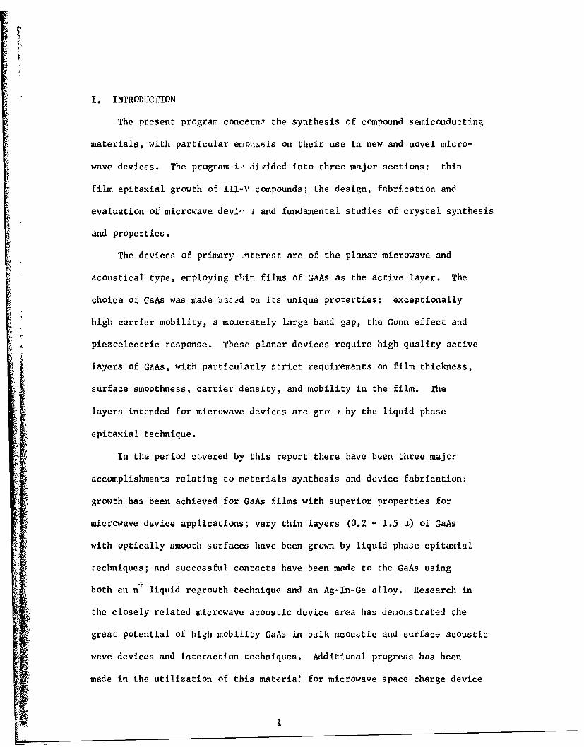
I. INTRODUCTION
The present program concern, the synthesis of compound semiconducting
materials, with particular emphasis on their use in new and novel micro-
wave devices. The program i. .iirided into three major sections: thin
film epitaxial growth of III-V compounds; Lhe design, fabrication and
evaluation of microwave devi, 3 and fundamental studies of crystal synthesis
and properties.
The devices of primary •nterest are of the planar microwave and
"acoustical type, employing t:;in films of GaAs as the active layer. The
choice of GaAs was made bazd on its unique properties: exceptionally
high carrier mobility, a moxerately large band gap, the Gunn effect and
piezoelectric response. Tbese planar devices require high quality active
layers of GaAs, with particularly strict requirements on film thickness,
surface smoothness, carrier density, and mobility in the film. The
layers intended for microwave devices are gro, by the liquid phase
epitaxial technique.
In the period covered by this report there have been three major
accomplishments relating to meterials synthesis and device fabrication:
growth has been achieved for GaAs films with superior properties for
microwave device applications; very thin layers (0.2 - 1.5 p) of GaAs
with optically smooth surfaces have been grown by liquid phase epitaxial
techniques; and successful contacts have been made to the GaAs using
both an n+ liquid regrowth technique and an Ag-In-Ge alloy. Research in
the closely related microwave acousLic device area has demonstrated the
great potential of high mobility GaAs in bulk acoustic and surface acoustic
wave devices and interaction techniques. Additional progress has been
made in the utilization of this materia& for microwave space charge device
A' ° - . .
applications. Also during this period, significant progress has been made
on the fundamental studies of crystal synthesis and properties of compound
semiconductors. The topics include: observations of precipitation
effects in GaAs by transmission electron microscopy; measurement of
electrical property changes in GaAs induced by changes in dislocation
density; a theoretical analysis of the GaAs/liquid gallium interface and
a study of the vapor growth of GaN, AIN and GaN - AMN solid solutions.
A description of the progress in these areas is given below.
2
II. EPITAXIAL CRYSTAL GROWTHR. S. Feigelson, B. L. Mattes, R. K. Route, J. Yen, and P. Petit
A. PROGRAM OBJECTIVE
The principal objective of the epitaxial crystal growth program is
the preparation of high quality, uniform and reproducible epitaxial lay-
ers of GaAs for the device applications program. The device program re-
quires layers (not obtainable commercially) that have carrier densities14 - 5 -3 30/7Kmblte bv 00
in the low 1014 cm-3 to 1015 cm range, 3000/77OK mobilities above 7000/
50,000 cm 2/V-sec, thicknesses in the .5-30,Urm range, and optically smooth
surfaces. All of these requirements are being achieved in the present
work by liquid phase epitaxial techniques.
In order to meet this objective, considerable effort has been de-
voted to the develo;)ment of new methods of growth, the study of variables
that influence growth, techniques to prepare and handle materials in-
volved in growth, and methods to evaluate the growth and its properties.
In addition, the epitaxial crystal growth program is coordinated with
the materials studies and device applications programs to prepare materi-
als with specific properties and dimensions and to interact on problems
of mutual concern.
The most recent objective of this program is to develop reliable
ohmic contacts for epitaxial layers that have carrier densities in the
10 1. cm-3 range. There is also a continued effort to improve the quality
of the GaAs layer, in anticipation of more stringent device requirements.
The future objectives of the epitaxial crystal growth program will
be: (1) to meet the device application and materials study program re-
quirements for III-V materials with specific properties; (2) to continue
3
the development and evaluation of ohmic contacts on GaAs epitaxial layers;
(3) to continue the analysis of the liquid phase grcwth process, in par-
ticular, nucleation; and (4) to develop new techniques for growing epitaxial
GaAs on oxide substrates.
B. PROGRESS
1. Achievements
High quality GaAs epittaxial layers, that meet the critical property
requirements for the device application program, have been grown by the
liquid phase epitaxial method. The epitaxial crystal growth achievements
that led to this objective are (1) ..mprovements in the purity of the
14 -3growth system and materials--to yield low 10 cm carrier density ma-S~2
terial with 300/770 K mobilities of 8000/60,000 cm /V-see; (2) refinements
in the temperature gradient cell--to yield layers with uniformity in
thickness from .5 to 30 Mm and with optically smooth surfaces; (3) n+
contacts on low carrier density layers--to yield excellent ohmic contacts;
and (4) a direct relation between ourface terracing mad temperature gra-
dient--to yield information on the nucleation process on the substrate.
These achievements demonstrate the success snd potential of the liquid
phase epitaxial methed for the growth of high qualit layers that in the
past were only achieved by the vapor phase epitaxial method. Over 200
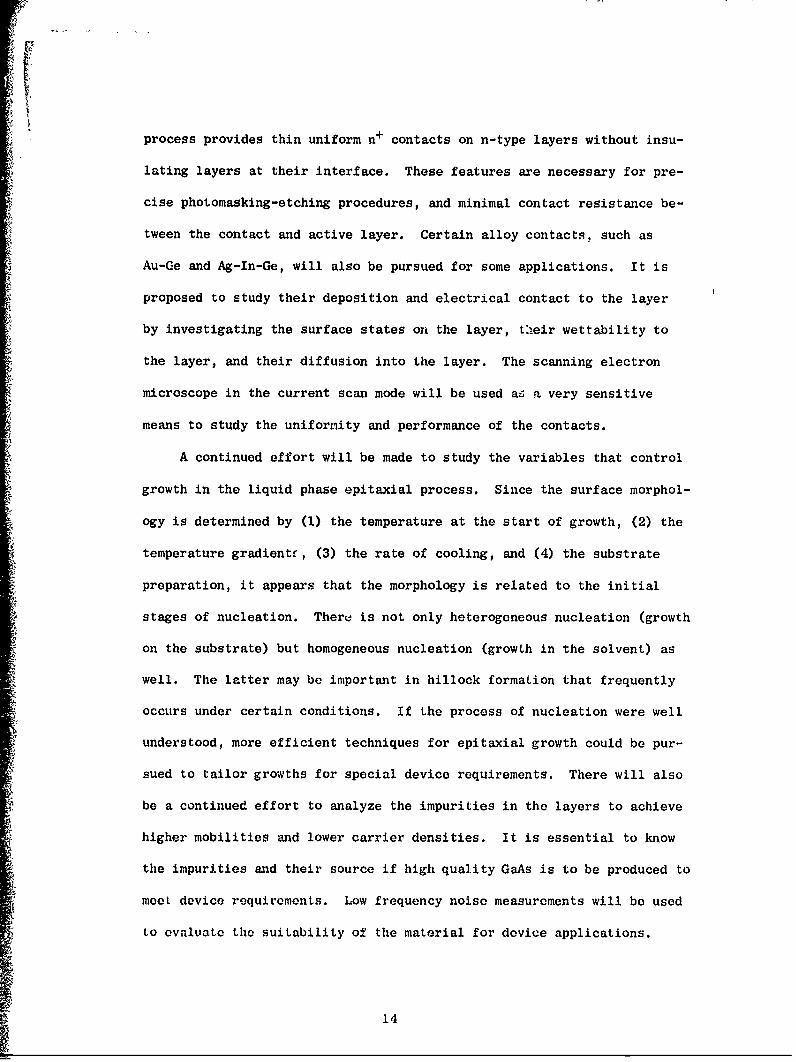
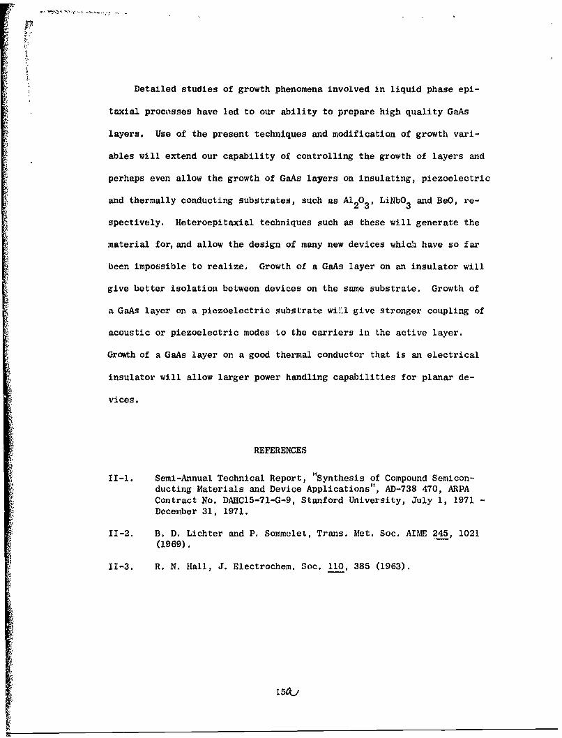
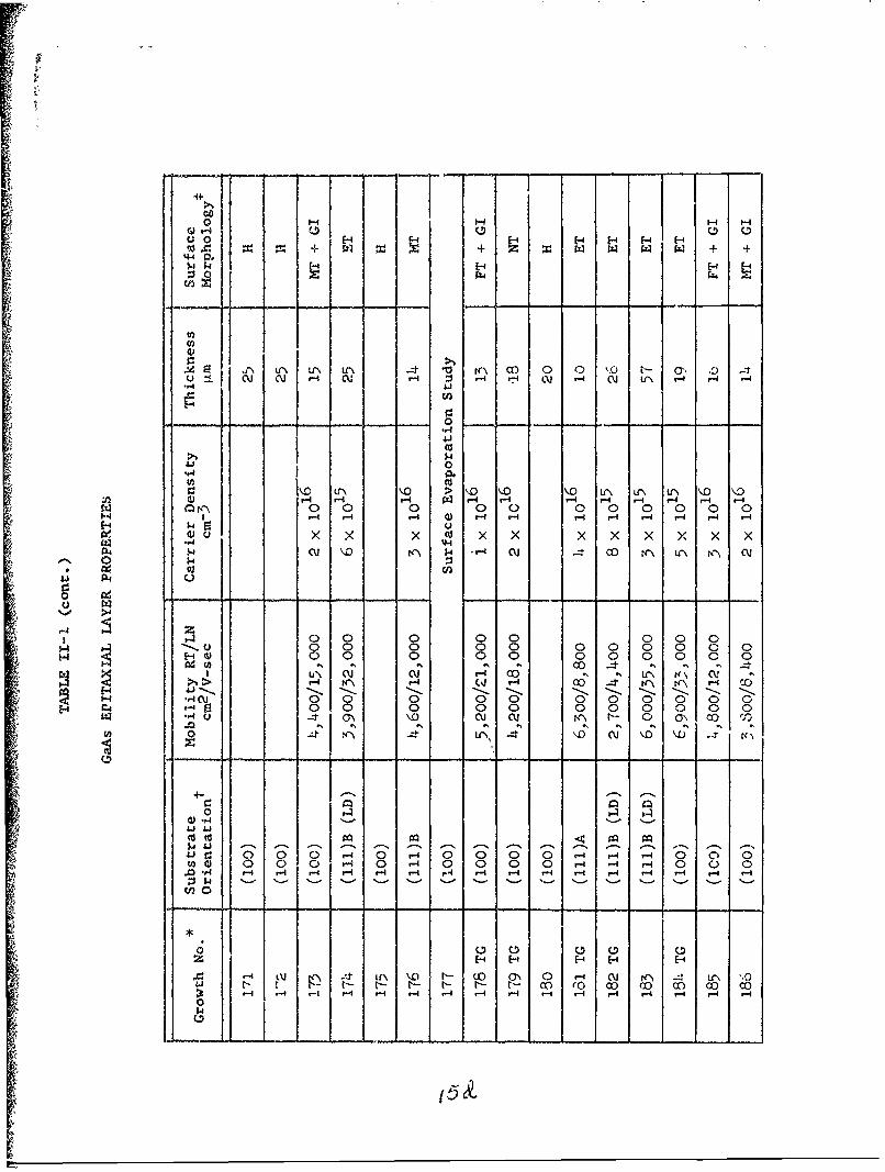
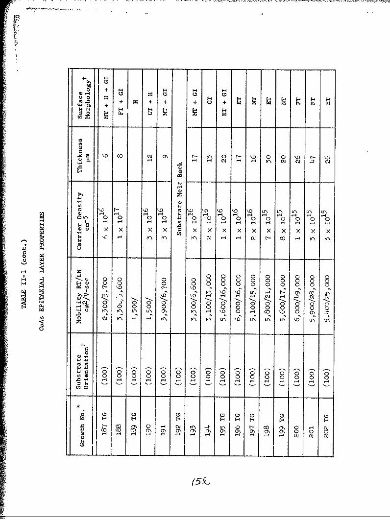
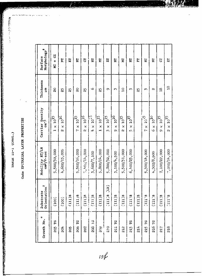
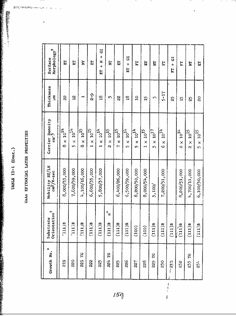
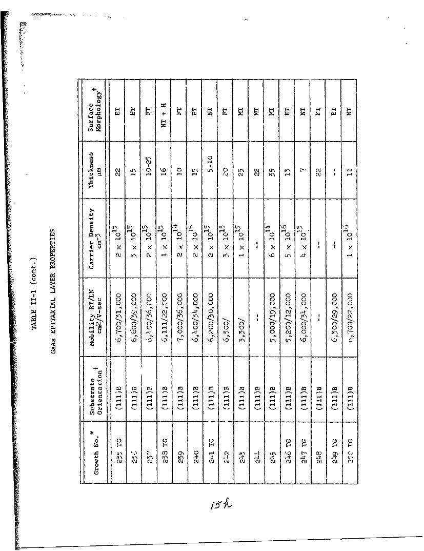
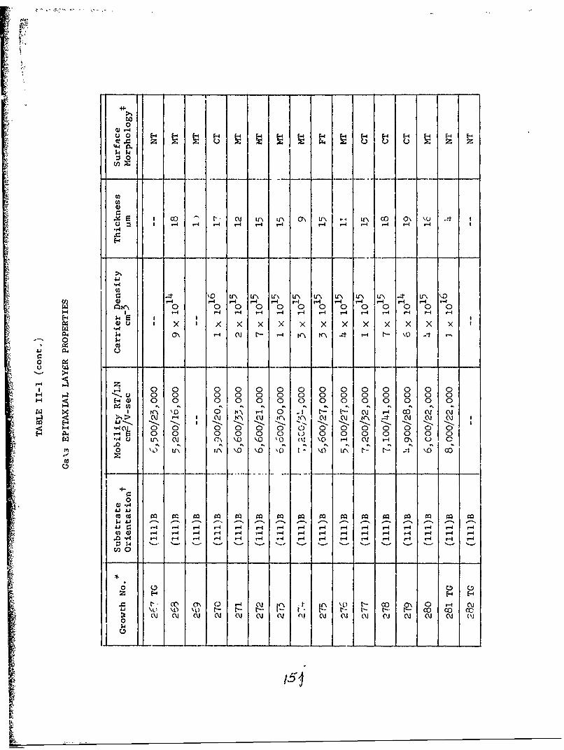
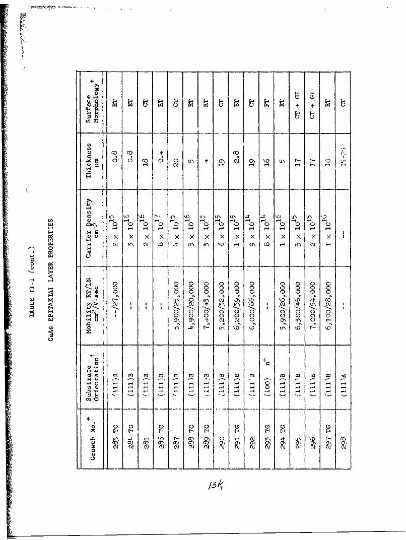
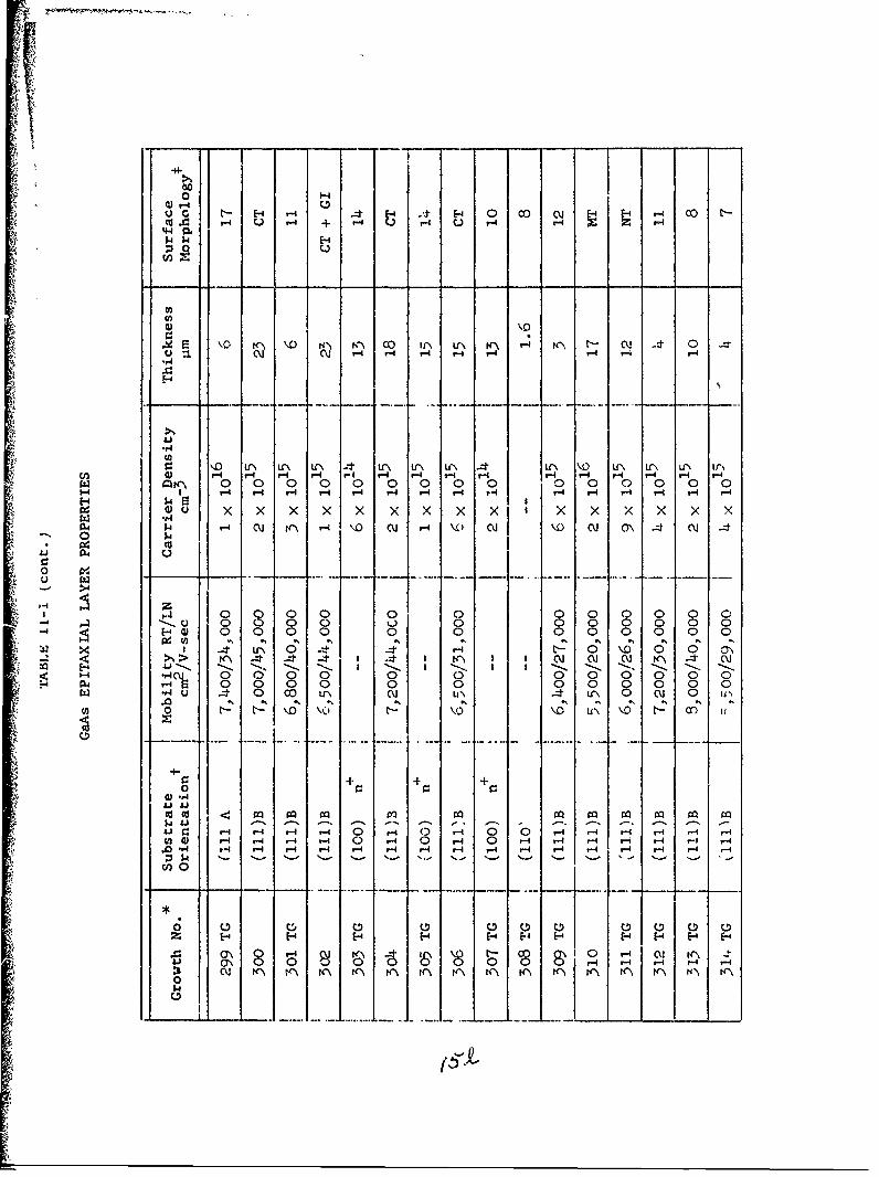
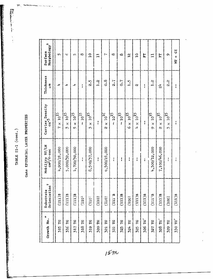
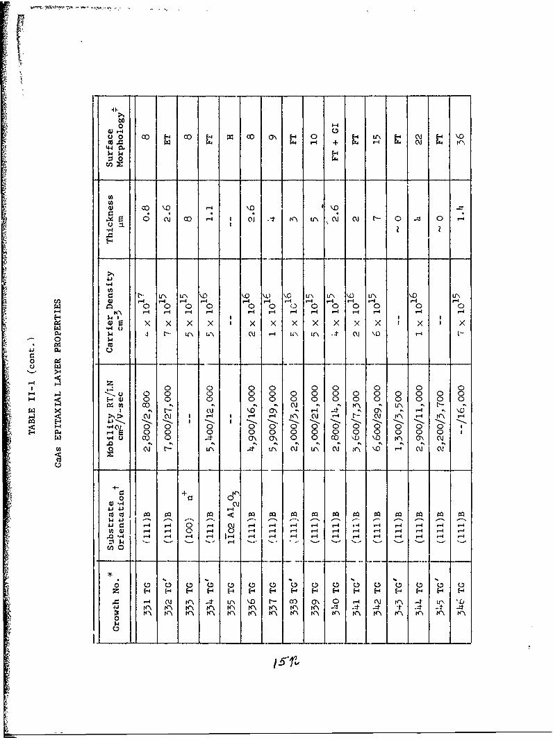
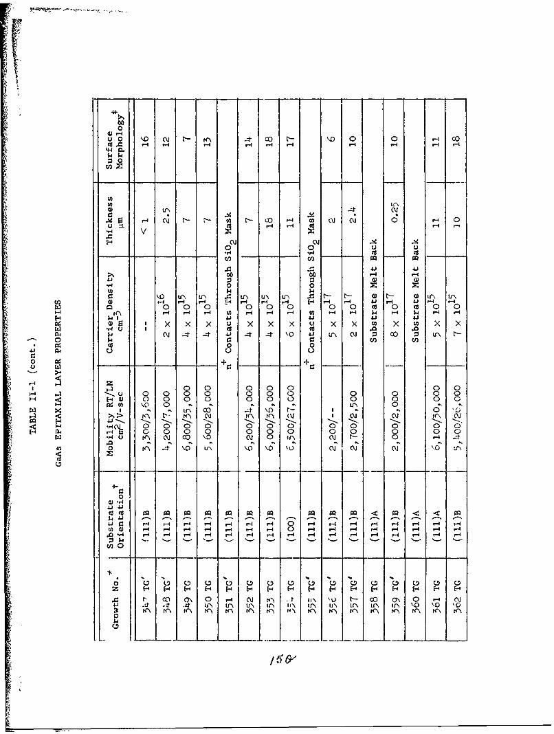
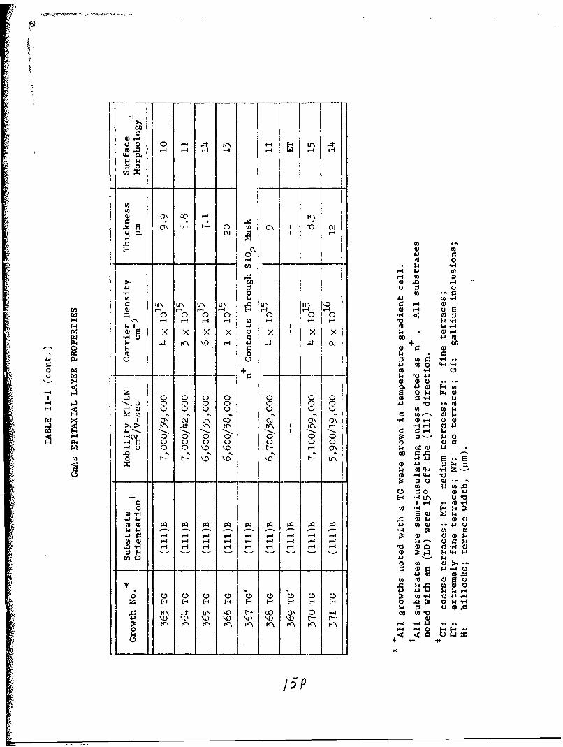
GaAs layers were grown for this program, and are liated in Table 11-1.
The majority of the layers were grown as part of the study of growth
variables involved with the liqjid phase epitaxial process. With the
+control of these variables, rcproducible high quality layers and n con-
tacts are now being grown.
I
A detailed study of the liquid phase growth process has shown that
a t,'mperature gradient normal to the substrate increases the nucleation
sites on the substrate. Thus, with control of the gradient and uniform-
ity of the substrate temperature, extremely smooth uniformly thick lay-
ers are obtained. Because of this it appears that nucleation and growth
are controlled by interface attachment kinetics and are not diffusion
limited.
2. Growth Method
Epitaxial Layers
A temperature gradient cell was developed to study surface morphol-
ogies in the liquid phise growth process. The cell provides a very con-
trollable means to establish a temperature gradient normal to the liquid-
solid "nterface. Since the epitaxial layers grown in this cell have been
consistently uniform in thickness, optically smooth and controllable in
thickness from 2 Mm to 20 gm in thickness, the cell is now used exclu-
sively for all growths.
The Temperature Gradient Cell
The temperature gradient cell is designed to provide a tempera.ure
gradient normal to tte substrate, Figure II-1, and to be used in a con-
ventional horizontal tilt system, Figure 11-2. The cell consists of a
graphite growth cell that floats on a liquid Ga reservoir contained in a
graphite cradle, and a quartz heat transfer tube which is immersed in the
Ga reservoir. The temperature gradient is produced by forcing a suitable
cooling gas, such as Ile or N2 , through the heat transfer tube. The liquid
Ga reservoir serves two purposes: (1) to maintain intimate thermal con-
tact between the boat and the heal transfer tube, and (2) to improve the
temperature uniformity under the substrate.
5
The principal features of the temperature gradient cell include:
(1) the bottom of the growth cell under the substrate which is machined
very flat and thin (-0.8 mm) to decrease the thermal resistance; (2) a
graphite lid which is used on the growth cell to act as a susceptor and
to minimize H2 flow turbulence in the cell; (3) the growth cell which is
partitioned on the bottom to separate the Ga from both the substrate and
the source during bakeout and saturation procedures; and (4) an expansion
space which is allowed for in the cradle to develop a head of Ga in the
reservoir that will maintain Ga in contact with the bottom of the growth
cell.
Operation
The temperature gradient cell is used in a horizontal tilt 3ystem
as shown in Figure 11-2. The furnace is (1) stabilized in temperature
to saturate the Ga solvent with As from a GaAs source; (2) tilted to roll
the As-saturated Ga solution onto the GaAs substrate; and (3) cooled to
epitaxially grow GaAs on the substrate from the As-saturated Ga solution.
The temperature gzadient is induced in the cell during the saturation
period. This insures that when the As-saturated Ga solution is rolled
onto the substrate, a temperature gradient will exist normal to the sub-
strate and the Ga solution will be close to the temperature of the sub-
strate.
To produce the temperature gradient, a controlled flow of He or N2
is passed through the quartz heat transier tube. The temperature gra-
dient is determined by monitoring the difference between the temperature
outside the cell and in the Ga reservoir. Once the desired temperature
gradient is achieved, the saturation temperature is regulated by varying
the lie flow with the furnace temperature controller at a predetermined
6
setpoint. The temperatures are monitored with inconel sheathed chromel-
alumel thermocouples inserted in quartz tubes.
The temperature gradient in the growth cell was actually mea'ured
during the initial evaluation of the cell. Thermocouples, in separate
quartz tubes, were located on and 3 mm above the subttrate, as well as
in the Ga reservoir. A calibration for the temperature gradient vs. He
flow is shown in Figure 11-'3. It was observed that the ternperatilr'e gra-
dient increased by 1°C/cm above the substrate when the As-saturated Ga
solution was rolled onto the substrate for a He flow of 28 litcrs/min.
This indicates that a definite gradient exists during the ini'Lation of
growth.
The temperature gradient cell can be used for both transient and
steady-state methods of liquid phase growth. The majority of the growths
have been by the former, where the furnace is initially cooled at a rate
from 300°C/hr to 3000°C/hr from a saturation temperature in the 5000C to
7500C range. Since no means is provided to wipe the Ga solution off the
substrate during growth, the thickness of the epitaxial layer is deter-
mined principally by the amount of As dissolved in the Ga at the satura-
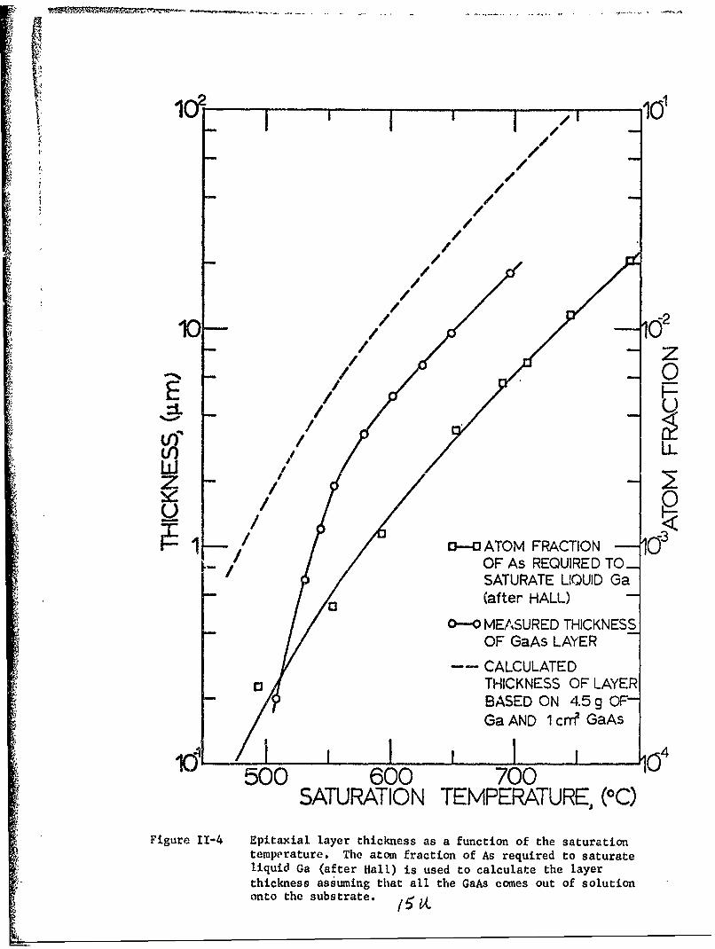
tion temperature, Figure 11-4. The saturation temperature thus provides
an accurate moans to vary the layer thc!imess from .2/Am to 20Mm.
n+ Contacts
The temperature gradient cell and techniques are also used for the
n + contact growths. The Ga solution is heavily doped with Sn, an n-type
dopant that produceE a shallow donor level. Since the distribution co-
-4efficient of Sn is quite small, <10-4, substantial amounts 1 10 atomic
% Sn are required to obtain careier danetties oi 5x1017 cm"3 or greater.
07 7
The cell is cooled rapidly during the growth process to insure a uniform
carrier density throughout the thickness of thte n+ layer.
To localize the contact regions, on SiO2 mask is deposited on the
layer by silane decomposition or vacuum sputtering techniques. Photo-
resist techniques are next used to selectively remove unwanted portiors
of the !,ask and the n1 contact material is then grown in the holes in the
SiO2 mask. At present, studies are underway to determine the minimum
size and shape limits for the n+ contact definition. Typical n+ contact
layers are approximately 0. 5 •m thick, corresponding to convenient SiO2
mask thicknesses varying from 0.3 jm to G.5 Mm.
3. Growth Studies
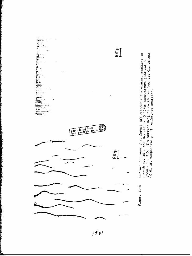
Nucleation and Terracing
A temperature gradient normal to the liquid-solid interface appears
to increase the density of nucleation sites on the substrate. This de-
duction follows from the observations that the terrace width is the same
as the spacing between nuclei1 and decreases as temperature gradient
is increased, Figure 11-5. The terrace width is uniform over the en-
tire layer surface, with the terraces extended in the foirm of long ripples.
The terraces extend normal to a [1003 diLection on (100) and (110) sub-
strate orientations and a [112] direction on (11i) A and B orientations.
The decrease in terrace width with an increase in the temperature
gradient appears to be related to the effect of theimal fluctuations on
the liquid solid-interface. It will be shown later that the temperature
fluctuation could arise from the heat of formation during nucleation.
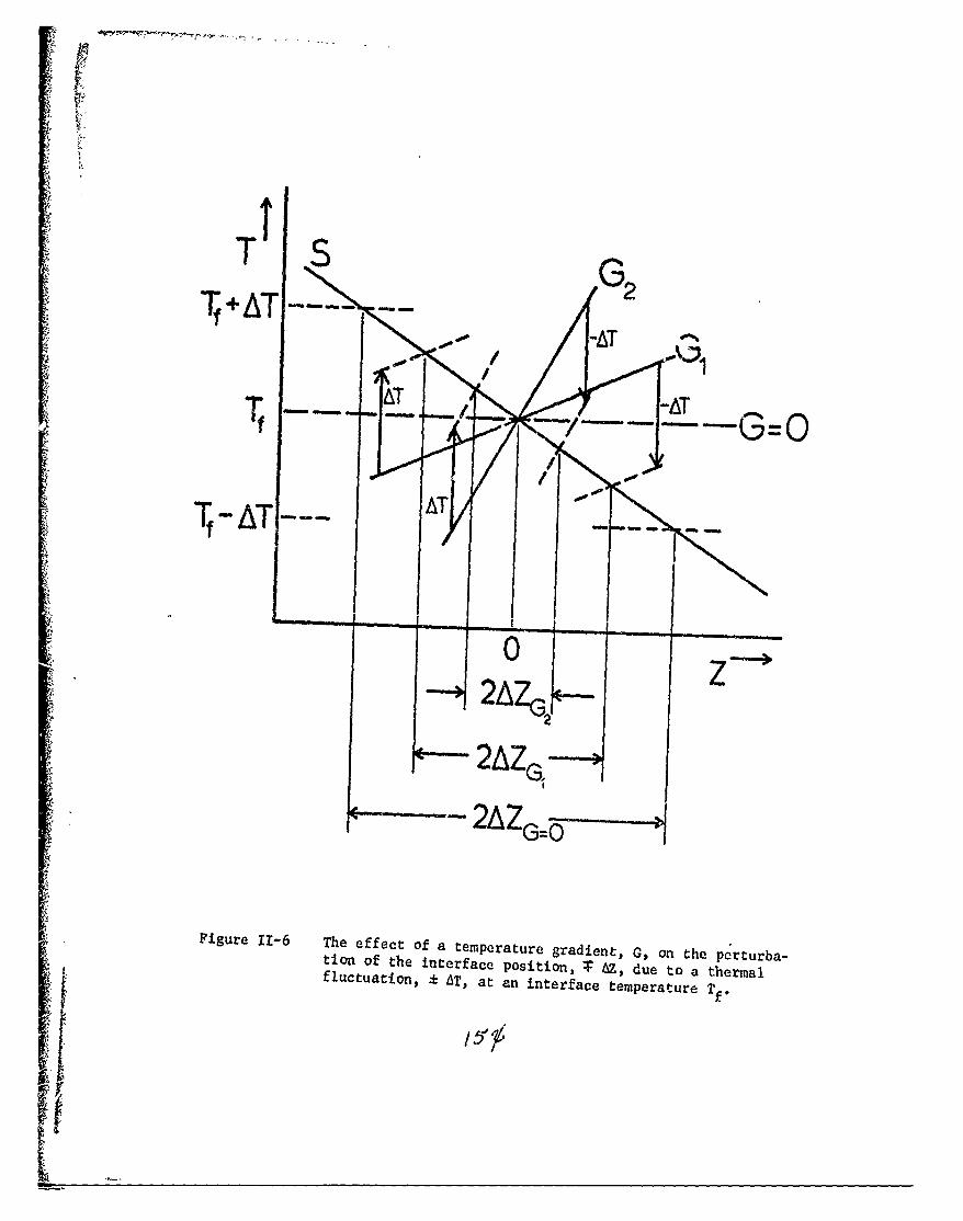
Figure 11-6 illustrates this effect in terms of a thermal fluctuation,
± AT, and a gradient, G, superimposed on the interface temperature, T,
at the position of the liquid-solid interface, Z. The perturbation on
8
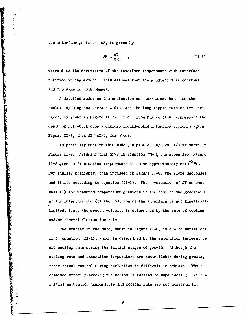
the interface position, AZ, is given by
AZ =• AT-lG-S
where S is the derivative of the interface temperature with interface
position ciuring growth. This assumes that the gradient G is constant
and the game in both phases.
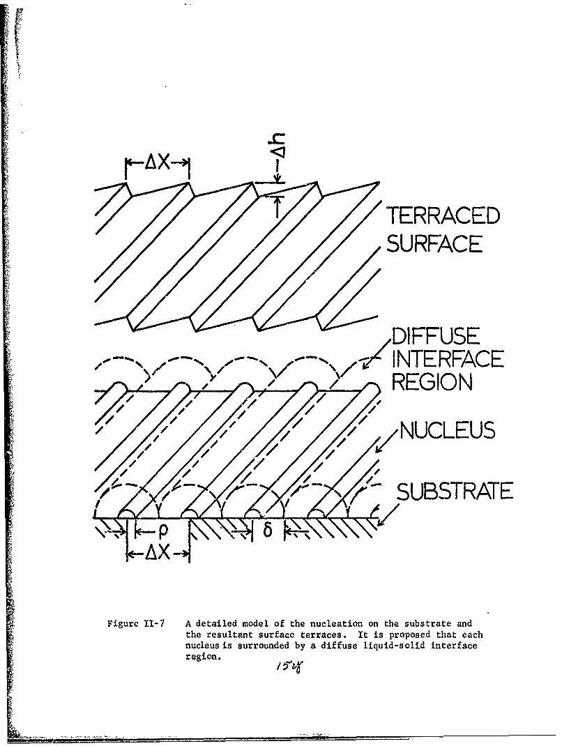
A detailed model on the nucleation and terracing, based on the
nuclei spacing and terrace width, and the long ripple form of the ter-
races, is shown in Figure 11-7. If AZ, from Figure 11-6, represents the
depth of melt-back over a diffuse liquid-solid interface region, 6-pin
Figure 11-7, then AZ-AX/2, for p<<b.
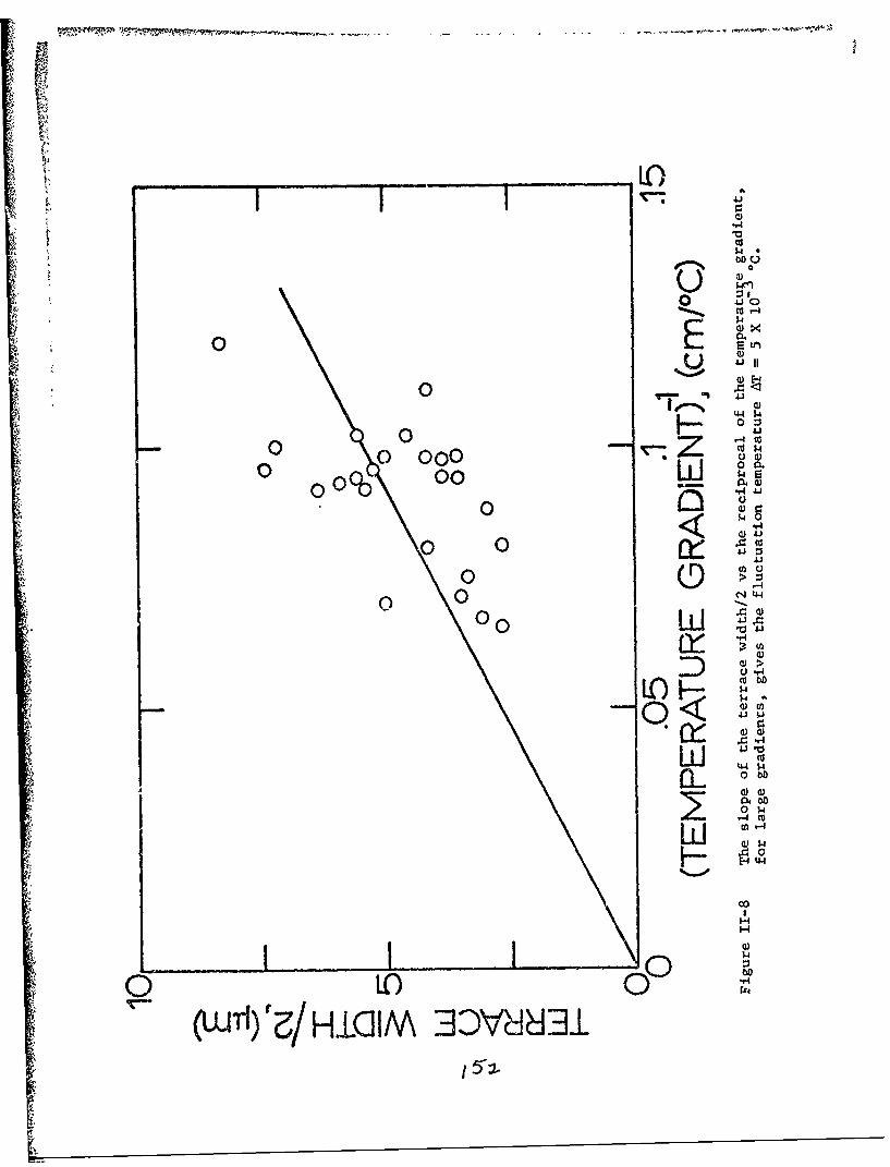
To partially confirm this model, a plot of AX/2 vs. 11G is shown in
Figure 11-8. Assuming that G>>S in equation (11-1), the slope from Figure
11-8 gives a fluctuation temperature AT to be approximately 5x10⁻³oC.
For smaller gradients, than included in Figure 11-8, thf slope decreases
and limits according to equation (II-1). This evaluation of AT assumes
that (1) the measured temperature gradient is the same as the gradient G
at the interface and (2) the position of the interface is not kinetically
limited, i.e., the growth velocity is determined by the rate of cooling
and/or thermal fluctiation rate.
The scatter in the data, shown in Figure 11-8, is due to variations
in S, equation (II-1), which is determined by the saturation temperature
and cooling rate during the initial stages of growth. Although the
cooling rate and satueatioo temperature are controllable during growth,
their actual control during nucleation is difficult to achieve. Their
combined effect preceding nucleation is related to supercooling. if the
initial saturation temperature and cooling rate are not consistently
9
applied during the initiation of growth the terrace width may range from
10 gm to 5 00 •m with or without a temperature gradient.
The height of the terraces, Ah in Figure 11-7, appears to be di-
rectly related to the terrace width. Because of this, the height might
indicate the size of nuclei that are spontaneously formed when the As-
saturated Ga is supercooled on the substrate. Optical interferometric
measure',,ants indicate that the height is approximately 1/1000th of the
terrE,-., width.
Any interpretation of AT ~5xl0- 3O., obtained from Figure I1-8, must
explain the following: (1) the terrace height and width ; (2) the inde-
pendence of AT on an activation volume associated with the height x width
x length of the terraces; and (3) the long parallel terraces normal to a
particular direction for different substrate orientations. A plausible
interpretation is given below.
A thermodynamic model based on the heat of formauion, AH, evolved
during nucleation on the substrate appears to account for AT -5xl0- 3 0C
if the following assumptions are made: (1) the diffuse liquid-solid in-
terface region, Figure 11-7, develops from the AH evolved by each nucleus;
(2) the nuclei are stably centered and spaced by the diffuse interfacial
regions so that there is no appreciable overlap--nuclei formed within
6-p would tend to melt back; (3) the rate of cooling, R, is less than
AT/T, where T is the period of a fundamental growth step, e.g., nuclea-
tion rate--for R >AT/T only a fraction of AH woild be available to melt
back 6-p; and (4) the nucleus' radius, p, is approximately the terrace
height or P-6/500. The temperature rise from the formation of nucleus
is given by
AT = ,(11-2)
cI p
10
where AH is the heat of formation and c is the iipecific heat. SinceP
AH is assumed to be distributed over the region 6-p, in Figure 11-7, the
actual temperature rise of this region is given by
AT = .H (11-3)C p
where p16 = 1/500 . The heat of formation and specific heat for GaAs at
10000K are AH = 4308 cal/mole and c = 6.6 cal/mole °C.2 SubstitutingP
these values into equation (11-3) gives
AT = 2.6x10⁻³ °C.
This value for the thermal fluctuation is in excellent agreement with
experiment, AT -5x10⁻³ C, considering that the above calculation was not
rigorously evaluated.
The preceding thernmodynamic model appears to be plausible, even
though a number of assumptions were made. Within these limitations, the
terrace height and width .nd the independence of AT on an activation
volume have been explained. The general terrace formations and their
orientation, however, are probably related to interface attachment
kinetics, where the terraces are restricted to line up parallel to a
(100) plane for all orientations. Why one (100) plane is prelerentially
selected over another is not known at present. However, this may be re-
lated to a slight misoriontation of the substrate. This observation is
based on diiivrent growths from the same batch of substrates that yield
the same terrace orientations.
Layer Thickness
Another growth study was the correlation between the layer thickness
and the atom fraction of As in liquid Ga for a given saturation tempera-
ture, using the liquidus line from Hall's data on the Ga-As phase dia-3
gram, shown in Figure 11-4. It should be noted that (1) the liquidus
line parallels the layer thickness very closely above 6000C; (2) the
measured thickness of the layer is less than the theoretical thickness
because of the excess GaAs formation on the surface of the Ga solution
in the growth cell--approximately 1/2 of the total amount of GaAs dis-
solved in the solvent; and (3) below 6000C the thickness faIls off very
fast--this is the region where hillocks sometimes form on the substrate
and/or layer and large numbers of platelets form in the liquid during
growth.
Heteroepitaxial Growth
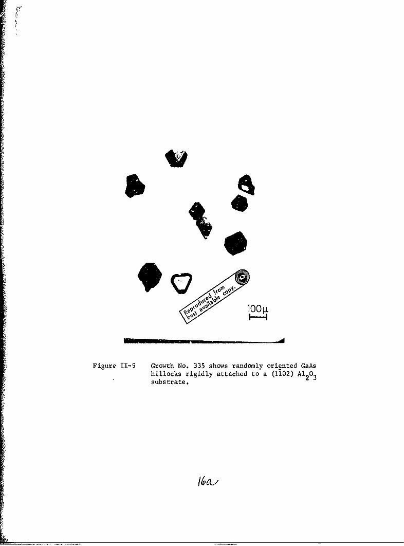
A preliminary attempt has been made to grow GaAs on a (1102) Al203
substrate in the temperature gradient cell, The result, Figure 11-9, was a
large number of randomly oriented hillocks rigidly attached to the sub-
strate. If the nucleation density can be increaved and the orientation
of the hillocks controlled by the proper selection of substrate lattice
parameters, a heteroepitaxial layer is possible.
Electrical Studies
Preliminary measurements on the n+ contacts hve shown good ohmic
contacts to 1015 cm-3 layers. Contacts to lower carrier density and
submicron layers are now in progress. Extensive Schottky barrier and I-V
studies are planned as part of the evaluation process. The caL.-Jer den-
sity of the n+ contact material is about 5x107 cm"3 and the doping 1_
very uniform throughout the contact layer. No insulating barriers have
been observed between the contact and the active layer, even though
melt-back was not allowed during deposition.
12
Considerable uncertainties occur whenever van der Pauw and Schottky
barrier measurements are attempted on low carrier density layers less than
2 Mmthick. This is due to a depletion region which forms next to the sub-
strate. The Schottky barrier then behaves as a Mott barrier and shows
little sensitivity to forward or reverse bias.
C. PROPOSED FUTIAUE WORK
The future objectives of the epitaxial crystal growth program will
be to (1) maintain the present capability for preparing material for new
device requirements; (2) evaluate and develop electrical contacts on
high purity material for device applications; (3) study and analyze
growth variables in the liquid phase epitaxial process; and (4) develop
liquid phase techniques for growing III-V materials on oxide substrates.
The basic responsibility of the epitaxial crystal growth program is
to provide materials that will meet specific property and dimensional
requirements for the device program. Therefore, the growth program must
maintain a flexible capability to meet new requirements, which may in-
clude other III-V materials and their alloys. The facilities and tech-
nology for this capability have been established for GaAs bi:c it may be
extended to certain other III-V materials and their ternary solid solu-
tions. The preparation of other materials may require the development
of new growth methods, substrate preparation techniques and more de-
tailed analyses of the growth conditions. For the majority of the de-
vice requiroments, however, GaAs will be the primary material.
The study of electrical contact problems will continue. The new
contacLing procedures will be further developed for liquid phase grown
n+ contacts on n-type layers. The horizontal temperature gradient
10
process provides thin uniform n+ contacts on n-type layers without insu-
lating layers at their interface. These features are necessary for pre-
cise photomasking-etching procedures, and minimal contact resistance be-
tween the contact and active layer. Certain alloy contacts, such as
4 Au-Ge and Ag-In-Ge, will also be pursued for some applications. It is
proposed to study their deposition and electrical contact to the layer
by investigating the surface states on the layer, t:ieir wettability to
the layer, and their diffusion into the layer. The scanning electron
microscope in the current scan mode will be used as a very sensitive
means to study the uniform~ity and performance of the contacts.
A continued effort will be made to study the variables that control
growth in the liquid phase epitaxial process. Since the surface morphol-
ogy is determined by (1) the temperature at the start of growth, (2) the
temperature gradientr, (3) the rate of cooling, and (4) the substrate
preparation, it appears that the morphology is related to the initial
stages of nucleation. Therv is not only heterogeneous nucleation (growth
on the substrate) but homogeneous nucleation (growth in the solvent) as
well. The latter may be important in hillock formation that frequently
occurs under certain conditions. If the process of nucleation were well
understood, more efficient techniques for epitaxial growth could be pur-
sued to tailor growths for special device requirements. There will also
be a continued effort to analyze the impurities in the layers to achieve
higher mobilities and lower carrier densities. It is essential to know
the impurities and their source if high quality GaAs is to be produced to
meet device requirements. Low frequency noise measurements will be used
to evaluate the suitability of the material for device applications.
14
Detailed studies of growth phenomena involved in liquid phase epi-
taxial procosses have led to our ability to prepare high quality GaAs
layers. Use of the present techniques and modification of growth vari-
ables will extend our capability of controlling the growth of layers and
perhaps even allow the growth of GaAs layers on insulating, piezoelectric
and thermally conducting substrates, such as A12 03 , LiNbO3 and BeO, re-
spectively. Heteroepitaxial techniques such as these will generate the
material for, and allow the design of many new devices which have so far
been impossible to realize. Growth of a GaAs layer on an insulator will
give better isolation between devices on the same substrate. Growth of
a GaAs layer on a piezoelectric substrate wil.1 give stronger coupling of
acoustic or piezoelectric modes to the carriers in the active layer.
Growth of a GaAs layer on a good thermal conductor that is an electrical
insulator will allow larger power handling capabilities for planar de-
vices.
REFERENCES
II-l. Semi-Annual Technical Report, ofSynthesis of Compound Semicon-ducting Materials and Device Applications", AD-738 470, ARPAContract No. DAHCI5-71-G-9, Stanford University, July 1, 1971 -
December 31, 1971.
11-2. B. D. Lichter and P. Sommelet, Trans. Met. Soc. AIME 245, 1021(1969).
11-3. R. N. Hall, J. Electrochem. Soc. 110, 385 (1963).
p5•
00
1.414 4E-
to)
00
001 0 0 0
1-41. 4.1 4.1a) (0 co co
U)1 14 $4 p 4- - - Hr4
H 0 0
41 0 0 0.r 4 m C
1.' r-4 CU v-4 1- 4 -4 O\ -4 1-4 ýq 1 1 -
140 0 4 0 0 0 0 0 0 0
a) 0 x 0 0 0 0 0 0 0a
HH W 44 -
W U3
0 0-0 000 0 0 00 0ci 0 0 0 0 0 -- 0 00 00
00 0 0- 0' C LA'0 0 U "0 LACA 0 -.t ..:t LA 04 LA L -4~L
\CD -- -:t \
.4-0
'54 -1 .1-1 1 -, -
*4.1 C: -4 H 0 0 0 1- 1-4 rH 4~ -4 4 1-4 -4 H 1- 14CAJ -4 r- 0 0 0 i-I 4 H- -4 1- 4 H- H- H4 H- H-
-4 -4 H- H- -1 ,4 H- H4 r H1 H-H
0
zr-4 Q'C0 'I . -:t LA\ \.o t- (C ~ 0 H- CU ". -r.
4.1 V-4 .-4 r4 .4 -4. .:4 .4 .-4 r-I -4 LA4 LAf LA LA L0
7-1
000 0 P E-4 E-4 H-- H E-H 4a40. Z + rT4 + 4Z4 W) W) W) 4) 4 ;. +
14- 4 - 4 04 (4 0 $4' E-4 E-4:j- 0 44 44.w
10 0 UM 0 N0 :
X) M
>1141 0. 0.
i-i co cto >> LA\ U'\ L NL LA\ \D LA\ LAl LA 'lLi i$4 U) ) 4 r-4 H
4 1-4 v-i P-4 r-4 1-4 r-4 r-4
U) % 4-I 0) 0 0 0 0 0 0) 0) 0 0V-4 a, c -t 1-4 f-4 ,-1 1-4 ,-I T-4 1-4 1-4E- $4~ .0 0
QU :3 X x X X x X X X X XU)*-,4 L) 4~4 4-4$4$444- 04 tl a-) 04 P-4 I- N LA- ý4
4.1 04 Ui
'-4C) 0 0 0) 0 0 C) 0) 00 0 C) 0 0 0 0 0 0) 0) 0Wc C) 0 0 0 0 0 0 0 0 0 0
fr ~ 4 0 LA 0 \rN -4 O. LA t=-NC\ r-4 oo 04 04rr -4 r-A r4 ' '-
4 4 v-I 0) 0 0) 0 0 0 0 0 C) C) 0-, E., C- tc. 0 -:t 0j _:t LA\ 04 Lf,\ 10 ON.0 UN tr .. *'zs f -: -: n' V W\
a, 0.4 4 - LA LA .:t -~ 4 L 04 QC
Q)) C)
414 41 1 .-
41~ ' -4 0 0 ýA 0 1-4 0) 0 0 4 4 1- ,4141414(4)4 r-4 0 0 1-4 0 r-4 0 0 0 14 14 ,4 14 4 . -.'-A 1-4 r-4 f-
4 1-4 r-4 r-4 r-4 1-4 '-4 "q4 ý4 H- -
4 1-4 r4i v-I
cn0
zA0 tA'i. - CO ON ) '-4 04 tC I UN \.0 i- CO cM C4J LA tiN LA\ UN LA ' \.D '.0 \(.) () 'Cl ') 0 \0 C '
3 -1 r-4 ,-I ~ 4 .- I r-4 1-4
v-4
r -4 .4 -1 1-4 r4 1-4 v-i 1-40
-~ --- r--r ----
uo 0
$. F44 E- -4 -
44) I-\ YIN C.)O o - ,UO N Hl H- VE (J -4 H~ Hr H- - -
C>1
0)0
U,\\co C> C '0 \ U- \ \10 .) -
O NIk0 LA 0. \ '0 '0 L0 A 0A '0 '0rl -4 r-4 r-4 0) r-
4 t
4 l r-4 .4 r-4 1-4 r-
4 -4
0JJx x x w x x >< ) x x x xCxi \.0 N'\ H... CUj _:t cc) tr U-\ Ni\ N
-I. U
1-4 zP4 ~ 0 0 0> C> 0> 0> C
co _:t1 ft 4 Co' L I\ _:t
W- \ r-4 (iJ r.4 Oo 4t tr\ ~ \ ~ .
H 4 C4\ \ j M1- 0Co fri
02 -4 t
01 o- 8 4 -
44l C) C> C -l C>4 r-4 r4 C>i C>4 C>4 v4 v-f r-4 C>l r-4 C
zC C-> 0- H> E-C 4 C> C > C> p4 4 E-4C C C
1.p -4 p-4 -1- -4 -.4 r-4 p4
-4
p.4 t4 1-4 p.4 r-4 -t4 p.4 p-q0n
00C + +- +- 444 44 w
s.4 14
COU
E-4-
\00
- ) r-4 .4 r- -4 5 4 v -I 1- f-4 1-4 V-4 1-4 r-4 r-4
r-4 v-I0N\ C 0 0 0 0- C) 0)C 0 0 0) 0) 0) 0 04-4 I - v -4 ft4 CO i r-4 r4 r-I g-4 -I r- 4 1- -4 .4 1-4
82) X , >( X X X X >( x x x x x x
4-i
ý4 z*00 0 C) 0 ) 0 0 0) 0H u C) 0 0) 0 0 0 C) ) 0) 0) C 0) 00-0 0) 0) 0) 0) 0) 0 0 0 0 0) 0) 0
rn \ M W\ \10 \0 Lr-4 C'J 1- CC, C\N > ) N ) Cj N) 0
N.0 t'\ r(\ LA n L C. \ tr\ 1-4 \.0 C) \4CO 0 C) OCooC r -4 v-4 N\% t4\ 10\ tr\\ Mo\ \10 Lf
4\ T\Mo
4' 4-
0
Iv- .-4 .- - 4 - -- 4 r . -4 r-4 v-4 r4I 1-4 - -
co '0 cu UN t- C) C\ Cuj1-4 r-4 t-4 r-4 v. -f r4 r-4 v- -4 Cuj Cuj Cu
04
W Iu00
G),- 0
Id 0 Lr\ LA\ 0 LA \,o LN m~ tf' 0 N,\ LArC\ c oJ~ .u CU CV Cuj Nu Wu Nu '-4\u
>14
541
1-4 P-4 1-4 f-4
t-4 r- i-Iri00 0000 0 0 010 000 0
1-4 1414 H r-I 1-4r-
0414 14 Cuj t- Cuj _: -C\ ~ Nt O'\ 01
0.t LA '0 LA .C '0 CO CO 0- LA0~@~
O4 u A LA 0N A L 0A LA 0.0 0 LA 0 00 00
004) 0 0 )0 00 00000 00 00 00
01 PC r- v-I 1-4~ t-44-- CO4 N4140, 0 -0--
O- w0C .0 0 0 0 0 0-, -\ E-4 12 o c U\ ;
t( .r\NU\ , l
0 1-4- 41 -L "
Ai 0 0 rý - -4/r/I - q r4 r4 4 - 14 ý(n 0 0r4rFI - ý 4 I 4 r4 V4 - - - -
00o4 H - -
O1- w-
:0 E-4 E-4Cj -
N- ý4 E4q E4f4 -- 4 4 EI 4 r E E E$4 . +E r4 +- rI4 N- -4 r-4 r- ýZ4 r- rN - - -
41 14
0-4~E- 0
r-4 UN CO\ N1\ CU CO\ 0 W\ N UIL C\ LN N
-A U- 0u '-4 '-4 c4 Lr\ 0u '-4 Cu
4- +
ý4 ~ ~ LA L .J LA U-1 :1 4 L - .4 - L L41 1-4 .- 4 r-4 t-4 1-4 r-4 ,..4 r4 - 4 - - I- , -4 ,N 0 0 0 0 0 0 0 0 0 -0 - 0 04 01- -1 v4 r-4 -4 i-U iU r-
4 9-I 0- -4 1-U r
4 r-4 - r-4 -
P.4 Iý O LU. C r4I '-4 rCu r r- 4 LA LA -4 1-10Cu L
00
0 O 0 0- 0\ 0 : 0r 0J I- 0o O' 0 0\ 0r 01
0~ LAj LAj '\4 Cuj Lu (\I ( A ) U '- N\
0Or-44v 0 H-- H- H-- +
co 44 + w 04 44 z
440 .
I14 S M c u \ 0 \.0 0 tr u\ L() cu tr\ r4-\ t- CMj Iu : CMj P-4 4- r-4 r-4 1-4 rj Cq N fr\ v- M -4
C L U\ us Un U\ Ll 11N U*N U . '0 UnCA) 0v r4 ,-4 ,4 r-4 1-1 r, r-4 r4 r -4 r-4 , V-
w 0 0 0 0 0 0 0 0 0 0 0 01-4 -4 P-! r-4 r-4 r-4 '-I r-4 '-4H E!~I
9. X X X ( X x x x x x ' ' xCM14K% ~ CXJ C\J '.0 -*% \D-4
o w
0 04
'-41 C 0 0 0 88 8 00 0 0 0 0 0 00 0 0 0 0 0
k- 0) 0 0~ 8 , 0 00 0 000 0 01- O\ ID ~ nC\0 - O\ C -
""4 -4 -4 -04 - 4 - -4ý 04 -4 -4
E-' -4 8-4 -4 04 04 4 0~ 0 4 -4 00 4
oo zr 0) :t O) tC) tC) 0 C
V~ '0 Q t-- O' o 0 0 ko C tcr UN '. f X)a\(
4'4

W I4u~ 0 ' H . H4 [-4 -4 E-.4 E- E-CM
"44
u~~ .1Cj r414-4 r-4
Q 0 00 0 00 0 oo o o0 0 'rI -4 ft4 r- v1- - r4 r-4 ,-4 v4 1-4 4 q
I.4 co NM C CM W\ f- (\j r-4 Cj CC) ULA N j-\ CM
o4 z
0 0 0 0 0 0 0 0 0 0 0 C)'4 '.u 0 0 0 0 0 0 0 C) 0 0 0 0 0 0
f-4 00 0 0 0 0 0 0 0 0 0 0 0 0t~ n ft U N -Iz (N gN %C0 -~a'~ .1 CMj .-I r- CO P-4 - 1 A ý '4
14. cm frý tr\ OM (NJ I I (j CM CMj r'- Al '-4 (7\ 1-4
"-CM 00 0 0. 0 80 0 0 0 0 0) 0 0 C.CL -4~ 0 0 0 0 0 0 0 0 0 Ci 0 U,\ 0"W.4 CJ CMj co (NJ \) 0 ig. OY\ NC) tr 0\~ C. (\ (71\
(0 C N \0 IpN -\o \j , c'. 0 r- ) -4
4-
0
r4 r4 AI r-4 I- CO r4 r 0 r-f CMI r4 -4 r4 r-r-4 (0 A4 LA r-4 LA LA LA4 LA4 r-4 -4I rO r4C 'SC) r-O "L
0 CJCz - E4E-4-
C ,j hý A L\ \O t ) a 4 Cj t\ - r
41 Lr l\ UN tr r\ LA t\ fN lr 0 IL 0 'D \ \ 'L
0
u E4141 &k
44 CL
:30
4~ rz I OD cm (UN NJ If\ (7\ LIN . CO ON\ \,U .. t ICJ I 4 V- H - r4 H -H 4 r- 4
r_ r..4 r- r-4
4JI
If* '0 A \L LA\ LA\ V\ LA\ tIN LA -4,\U/) W -I r4 H ý4 H r4 H -H 4 H r-4 H H 4
*(N 0 000000 0 0 0 0 0 0
C) I IX x X )< X X X X ( )( x X x.4-1- r_4 5-4 tr\ H- "No-H 1~ ~ '~ 4 - '0
4 0
00 0 0 0 0 0 0 0 0 0 0 0 0H u .C 0 0 0 0 0 0 0 0 0 0 0 0 0 0
H- E-)O 0 0 0 0 0 0 C) 0 0 0 0 0 0 00~ w\ - 4 04 -1 1- .~4 0* N N
* < *.I(NJ0 0 0 0 0 0 0)0000000*E-4 A4 r. 0 0 0 0 0 0 0 0 0 0 0 0 0 01
-''U ULA (NJ r\ \.D \-.0 '0 (%1, '\0 H- (NJ rH GN 0 010 '? AI '0'0 '0 t- a. A C - 1 ' C)
00
co0
..0,-4 H4 H- H_ H- H4 H- -4 H4 H4 H- H_ H H H4 H- H
Cl0
z E-4 E-4
\C- \0' 0T- F0 tH ,N t 2 A '-O o-,- 0,D H.- (NJN '..' \i 'L) CM N-j C i~ V~ (\j -- C-- C-j N N- CN CO N,
0
0o> H- 1-4
Q 0 H- H -4 P4 E-
$4 E-4 E-4
(L) Oo co co
CxM v4
H- 1-4 14 "4 r- 1-4
E-.4
14
04 1 C\j K-\ C) co -t NO l I\ \0' UNI CP\ C) \J trý LA r..
zN 0 0 0 0 0 0 0 0 0 0
WC) 0( >( 0 0( 0 X 0 0 X 0 0
-4 0 w. (7 \0.O \1 Ht c
414 ~--- 1-
rI000 0 0 0 0 0 0 0W 44 U 0% O'\ ~I (Mxi CN N\ -.0
ft tf I ,
4-1
U)0 W t H H4 H- r- H- H'4 H1 H- H- 0 H- r- fH H H4
.0~ý4 E-4v H H H H p Hp
0 , 8 ( 0 0- 0~ :0 0r \0 t-0
Aj C C-0 Co zO Ox ONo' mG('1 WI01(i 0 ~ j Im Cj C M O ~
~44
i?:0
%' 1 - C r r r tC\ C~ -1 z
u\ :i C~ cu r- -4 r4 r4r - -
F4 r4 T14 r-4 uI T-.4 ,-4 r'.4
- r- ?-.4 r-4 ,-4 u-I .-4
0 0 0 0 00 0 0 0 0 0 0 0 0 0
04 r4 ~ .4j tc V 4 Iý C~ I- I~ \l( C\i ON1 _tN .j (Xt
0- 0 0 0 0 0 0 0 0 0 0 0-4 ) 0 0 0i 0X 0N 04 N 0 0. 0 UN
4Co 0006 0 0 0N 0
+ +0 aC
41~ 0 -4 1-4 u-I V-4 0 r-4 C0 1-4 0 0 9-4 r-4 u-I r-4 v-4i v-ICo OJ .-4 r-4 u-
4 r-4 0 1-
4 0 u-i 0 u-4
r4 u-I r-4 1-4 r-4 u-I"~. 4 f.
4 r-4 u4 -4 u- u
4 rI.4 P-4 f-4 T-4 r.-
4 f-4 u-I uI r-4 P-1 -4
0 C-5 0. 0( U 0z 0000p 0 E-4 P E-4 E-4 T-4 p 4
0
00
00 LP. UŽ L\ CC) 0 --4 ct co 00 (\ 0 E- '-4 E-4to C -4 f- '- 4 rA -4 1 +
CjC;
.a.
E-i
tC\ Lfi If LIN. LI'\ nU L LI'. UN' LI\ WN' UN. UNUl) r -4 r.4 r-
4 9-4 v-4 9-4 14 9-4 ,.4 i-4 r-4 r-4 r-4
N0 0 0 0 0 0 0 0 0 0 0 0 044'. 1- .4 4 i4f r-4 r-I ,4 -. r.4 V-4 .. 4 ry4
02 x x x x X x x X x X0.4 K,\ ti' \ U'. Cuj (Or%:j0 CuM C0 a
C4a* A-~ 04 .
0 W~cO W
I- >
- 0 00 0 0 0 0E-4 (D ~ ~ - 0 0 0 0 0 0 0
HO 0 0 0 0 0
44 4-' *'lC' 0 0) 0 0 0 0) 0
14 --- U
4-.a
0) ,
4J - - 4 0 00 0 r-4 r-4 0 r-4 r-4 .- i u-4 0 r-4U)l 4) r 4 14 9-4 -
4 9I r-4 rI 1-4 0 in
4 1-4 .- 4 r.
4 0 .- I.0 P4 1-4 .- 4 -1 9-4 r-4 ,..4 1-4 ý4 94 ,.4 1-4 9. P-4 r-4 1-*4 t-4
00
z -4 H E-4 H E-4 P- E-4 H E- E-4HH H
Ic '.- \.) t- CO0* 0 r-4 (U \1.. U.'0 t- CO 0m 0A' -4 '-f .- I '-f '-4 N Cu N Cu Cuj 0i Cu Cui Cuj Cu rt
0
W r-4
:3- 004
o OD Q -
CO co COj --t +- U- ci t- :
CA
wi 0 '0 0 -0 '.() 0 0 0 00t.- K\c~ -4 1- I r-( .1-4 tC -L CM t-4 tf-4 C r-4
C4a
C)0 00 0 0 0 0 0 0 0 0
P.4I I. f-4 t** -4 LA\ r-4.L\ A ~ t CU '
4.'- -. 00, 0 8
> 0~ \ c 4 C- c
P- 4 r- .. u 0 0 0 0 0 0 0 0 0) 0 0 0 00'-A H 0o 0 01 0\ 0O 0 0 0o 0\00 0\ 0 0
0- N t(\ CM\ N- UN OM C\ \0 C \ 0
-4 4H000 0 0r
*0~ CO ,. O \ ' O \ . C jC
4J4
U 0,4. 44 r .- r.
z0- P4 &4 E4' p- IsEr 4 . 4 - -4 E-4 F-4 1-4 E-4 E-
1- 5.M t.\ -- U'\ a) -44 cm K, *. %-**-t
Kc N h\ tc N I\tnOW N - .t -t I Z
KN fr( t\ tC'N f\ t(,\ NN\ N'\ 1 1\' -r\ .t-\ .4\ KN .4 t:' .00
00
4J-4 I
co LINa) CM
.!4 - Cu 00 W O 4 C; 1-4 C)u -I 1-4 f-s
y-4 V
HCuj CM0 0 U*rl -,4 CU C
U0C) 0 - M
Z 4.3 4.10%00 0 v- r-4
.1-40 0
\10 LC\ UlC ~ if\ UN, U,\ if U ) I- O r. tNW0 0 -4 r- r-4 H v
4 H 1-I0 E -4 '- -4 4Jv- 4.3 v4 '-4
00 C) C) C) C) C) C)C ) CU C) 01- -4 -4 1-4 Cl) r-4 r-4 U) r-4 r-I w. r-4 p- v4 1-4
E- 41g . 4.3 4.1C4 ~ >( X X U )< X X U X X X U) X X
94 -r-4 I U CU 0.04Cu _t _:t 4.' _:t _:1 ' 413 L\ N\ :3 CO :J LA\ E
0 a :U)cIxU 0 0
0 wr + +~u~ U 0 - 0
C) 0) 0C00 0 00 0 01-4 C- C) 0 ) 0 ) 0) 0 0 0) 0 0) C
0Cf \10 0) % . * Ln C)0I %. %. U, 00 :.t . -I )
o o4\ o)C ) ) C 0 0 0) C) C 0 C)W0*.U I' u C . Cuj 0) I Cuj t- C) _- t
(A) 0 _:t .4 0 LA n . 0C C uj CM MO n'
.4-
0
41 r. g.-I 1-I 14 1-4 1-4 -4 v-4 r- -4 i.-I r-4 v-4
1-4 P-4 1-4 1-4
:j14
H H P H F4 E- H - 4 F
j r- CC) MN C) rN '4.) W\ .f 11- CO (N C) r-4 Cu4.) _;t .4 in uN \ U WIN I C l "I\ iN UNN W\. r 1 1'0 0 '
05.4:9 W U
" N h\ W \ 1-
.4f
ri00 0 r4 .r - E-1 Lr\ -:t
4.4.
0) CU c
00-,4 0 - 7
r-4 w)
0 41 P4gIU\ 94\ n. UNU- W \0
Wn 1- - -4 rI1-4 r4 ,.. r-4
Hi S)H 0w0 0 0 0 0 0 0 r4< -1 C
H r\-4 H- r- 1-4 M) - v- r- 4 1.4 ,4E-4 to1 p- r.47-
W2 X X X u< 0 X x x 1.. * ) W-4-,4 -U -00
04.4 - t4,,\ \O r-4 +
2 0
0 04 + -A..u W z 1.4 41J
' ~ >4 9) WO .*0. 4-J ) E-i
4 0 0 00 0 0 0 D0- uI-- u ~ 0 0 0 0 0. 0 * 4 10 -E-4 0 0 0 0 0 0 0 V) (1)1.
I Q U Lr\ cO CUjCr m. 0) 4 U 4
00 H 4-'- r. *- - - *. I -. *-. H
r H*-AC4 08 08 0 0 00- 0 i- W 0E-,~42 0 0 0 0 0 0 0 0 0
*70 0 0 \0 \10 G~ \ .40to0W 4.3ft ft ft' 00 0r.C
W) 4J -- 44 ) -4 4.4 'V
-~: - 0 W.)
H- -r4 Lr\ u V1'P-4 *..CU-A
0 tv -'-4 E-414J 74J 42) w 4)Ccu cc PO 00 00 00 m0 00 00 O 4 m 4)W -~-4J U
41 J -H -H - r- H 4 H 4 rH H4 r- t a) W ).p
.0 -A H4 H- H- %- H- H4 H- H- H- 10 Q) a 0 -A
p I-1ý - I I- 1ý ) Wý 41W0 414U
U) CU W 0(A* -A3 L4 141J -
.- t -N 0 0,.4- to 0 0 W4J) (, \L ' \) \S 0 C-' - w
* 4- -if.
Figure Captions
Figure II-1. Details of the temperature gradient cell.
Figure 11-2. Horizontal tilt system with temperature gradient cell inplace.
Figure 11-3. Dependence of the temperature gradient normal to the sub-strate on the He flow through the heat transfer tube.
Figure 11-4. Epitaxial layer thickness as a function of the saturationtemperature. The atom fraction of As required to saturateliquid Ga (after Hall) is used to calculate the layerthickness assuming that all the GaAs comes out of solutiononto the substrate.
Figure 1I-5. Surface terraces that formed (a) without a temperature gra-dient on growth No. 261; and (b) with a 15 0 C/cm temperaturegradient *n growth No. 315. The terrace heights on the sur-face are 0.1/)m and <0.01/m, respectively. Interferencecontrast.
Figure 11-6. The effect of a temperature gradient, G, on the perturba-tion of the interface position, FAZ, due to a thermalfluctuation, ±AT, at an interface temperature Tf.
Figure 11-7. A detailed model of the nuclea'ýion on the substrate and theresultant surface terraces. It is proposed that each nu-cleus is surrounded by a diffuse liquid-solid interface re-gion.
Figure II-8. The slope of the terrace width/2 vs. the reciprocal of thetemperature gradient, for large gradients, gives the fluc-tuation temperature AT = 5x10⁻³'C.
Figure 11-9. Growth No. 335 shows randomly oriented GaAs hillocks rig-idly attached to a (1102) Al203 substrate.
-23
It11
/r
00
I -44tit 0
r4-
-J'
UU
$4-
-w 0'-
T - 0
w x
:D U
ILi
w I
Uz
V) X
LL4
0$
LL4
5
w '-4
4.)
c4J
14
15" EOU
z
W
(DH
IL5
O 10 20 30He FLOWJ (liters/min)
Figure 11-3 Dependence of the temperature gradient normal to thesubstrate on the He flow through the heat transfer tube.
1*1
V -2
10 ,101! /
// /"
L4 ,0 /
E/
0! / ---13 ATOM FRACTION - -
OF As REQUIRED TO-SATURATE LIQUID Ga
A ~(after HALL) -
0--0 MEASURED THICKNESSOF GaAs LAYER
--- CALCULATEDr• THICKNESS OF LAYER
BASED ON 4.5 g OF--Ga AND lcr-? GaAs
0, 500 600 700 oSATURATION TEMPERATURE,, (°C0
Figure 11-4 Epitaxial layer thickness as a function of the saturationtemperature. The atom fraction of As required to saturateliquid Ga (after Hall) is used to calculate the layer
thickness assuming that all the GaAs comes out of solution
onto the substrate. /
00
cd C)
4~Cd C)
Q ý4 P4~
C)1ZC)
0l000L
a. 1
4Jc) i
S.C)
ý4 C)
..Z C) 4J
- CpbeSt 0 -t.~C)
C : C-4-,
(/) Q.) *C)
p cI C"J ( C)
C).
4- Li JJ .-
- HH4ý4C
1'4
T S P2m+AT ---' - -
A-AT
T -AT AT- =
2AZG z2AZGA
S2AZG-O
Figure 11-6 The effect of a temperature gradient, G, on the perturba-tion of the interface position, T AZ, due to a thermalJ, fluctuation, A AT, at an interface temperature Tf.
I
IC
,--AX
TERRACEDSURFACE
DIFFUSE'- --'INTERFACE'/" ,")" 2/ REGION
•,•,, //NUCLEUS
. / "SUBSTRATE
.. •AX
Figure 11-7 A detailed model of the nucleation on the substrate andthe resultant surface terraces. It is proposed that eachnucleus is surrounded by a diffuse liquid-solid interfaceregion.
e'.2
I -4J
0 0)0
00ooP
00 -A144.
"4.
ot41.
o ' 4 j>o C' 1J4
LL.
0 4
$~4i~%a cboL~t-::4LO 0 P4
H iI IM ýA3
A *1
Figure 11-9 Growth No. 335 shows randomly oriented GaAshillocks rigidly attached to a (1102) Al 2 03
substrate.
16a0,1
III. APPLICATIONS OF COMPOUND SEMICONDUCTOR MATERIALSG. S. Kino, C. Quate, M. Bini, G. R. Bisio,A. Chiabrera, and S. Ludvik
A. GENERAL OBJECTIVES
The purpose of this work is to design and fabricate new and unique
microwave space charge and acoustical devices. We are interested pri-
marily in planar devices in which the conduction is along a thin film of
GaAs deposited on a semi-insulating substrate. These devices are fabri-
cated using modifications of silicon integrated circuit technology, and
for their successful realization we require high quality GaAs epitaxial
material of specific thickness and carrier density on high quality sub-
strates having several different orientations. These requirements are
unique and, hence, make a closely integrated materials growth effort es-
sential to the success of the program.
B. PROGRESS TO DATE AND FUTURE WORK
1. Gallium Arsenide Space Charge Devices
During the past reporting period additional progress has been made
on the uzilateral space charge amplifier program, after some initial dif-
ficulties with the contact technology and material quality. The material
requirements are typically for high quality GaAs layers 0. 2 - 2 0Am thick14 15 -3
with carrier densities in the 10 14-1015 cm range deposited on semi-in-
sulating substrates. The material must be of very high quality in order
to be resistant to avalanching in the contact regions where high fields
inevitably occur. Furthermore, the substrate-active layer interface
must be free of defects and impurities in order that breakdown through
or along the substrate may be avoided. Finally, the surface of the epi-
taxial layers must be smooth enough that photamasking techniques having
16
sub-micron resolution may be used; the devices are by necessity quite
small, the width being of the order of 1 nun and the length 1-100Am.
Several months ago a limited quantity of exceptionally high quality
GaAs material meeting all three of our requirements became available
from the Center for Materials Research (CMR) crystal growth effort of
this program. With this material we have been able to construct for the
first time devices which show no signs of avalanche at the contacts nor
any indication of substrate-interface breakdown or substrate "punch
through" breakdown. Before this, we had tried epitaxial GaAs material
from a number of other sources (mostly commercial, but including earlier
CMR growth facility material) and in no instance was the material quality
high enough nor was our contacting technology perfected to the point
where we could construct a diode that would saturate without oscillation
and without breakdown.
We are currently using an Ag-In-Ge evaporated alloy in our photo-
masking procedure to make the ohmic contacts to the new high quality ma-
terial. Previously, we had developed an evaporated Au-Ge alloy contact15 -3
and we could make good contacts to epitaxial material having n >1015 cm .
However, for the lower density, high quality material required for the
present devices, the Au-based alloy does not seem to be adequate. Part
of the problem may be the fact that the Au film tends to iball up" during
the alloying step, reducing the effective area of the contact and in-
creasing localized fields. With the Ag-based alloy this is not a prob-
lem, even though the alloying temperature is higher (500 0 C). Usiag this
new alloy we are now able to make very good quality ohmic contacts to
the lower carrier density, higher quality material.
The goal of the unilateral space charge amplifier program is the
17
design and construction of a solid state equivalent to the traveling
wave tube for use at X band and higher frequencies. For the design of
these devices we have performed detailed calculations of the exact dc
field distribution within r thin epitaxial diode using the empirically
measured velocity-field characteristics for GaAs. These calculations
show that the dc field increases monotonically from the cathode to the
anode, passing through the threshold point for negative differential mo-
bility approximately one third of the way from the cathode for a long di-
ode biased just above threshold, as shown in Figure III-1. We see then
that to make a successful microwave amplifier, the input of signal must
be injected as close as possible to the threshold point at a level well
above the background noise level there. Also, the total gain of the de-
vice must be limited in order to prevent Gunn oscillations or saturation
on noise originating in the cathode region.
A few devices based on these calculations have been constructed,
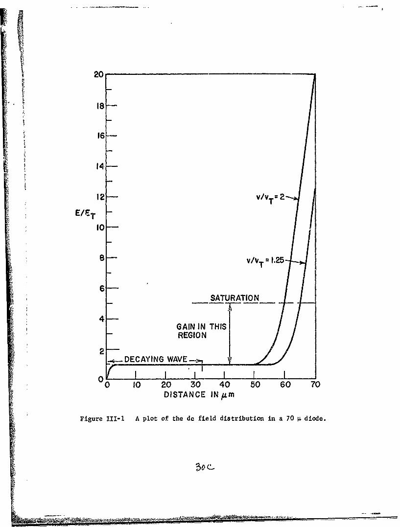
two batches of amplifiers with the rf input on an insulated gate and one
batch with the rf input on a Schottky-barrier gate, The first kind is
in the form of an insulated gate field effect transistor with two evap-
orated aluminum gates instead of a single one, as shown in Figures 111-2
and 111-3. The gates are capacitively coupled to the active material
through a thin SiO2 layer. The longer, grounded gate in conjunction with
an active layer nd product < 1012 (n is the carrier density in number-3
cm and d is the layer thickness in cm) is intended to suppress oscil-
lations by limiting the total gain to a value of less than 50 db. The
size of this electrode also determines the input and output impedances.
The narrow, upstream gate is used to inject the rf signal which is then
detected at the drain electrode. The narrow gate is positioned so that

the input signal is injected just at the beginning of the negative dif-
ferential mobility range. The total device represents the first solid
state equivalent of the conventional traveling wave tube with a calculated
gain of perhaps 40 db in the frequency range 8-12 GHz.
Two batches ,f devices having insulated rf gates were made from two
CMR epitaxial GaAs layers, wafer I with n = 8xlJ4 cm 3, JA= 8000 cm 2/V-sec,
thickness d =10 m and wafer II with n = Ux1014 cm-3, A=8000 cm 2/V-sec,
thickness d =10m. All devices were 70 Am long with the longer gate
35Mm long, the shorter gate 5Mm long and 51m spacing between gates and
contacts. With batch I, due to alignment problems, the spacing between
the long gate and the drain in the final device was 10Am. Typically, we
made approximately 9 devices at a time (three rows of three) on a sub-
strate. The contacts were good in all but 1 out of 18 devices (a device
near the edge of one of the substrates). Some of the smaller gates, 5 Mm
wide, had breaks so that the yield was 5 good devices from batch I and 4
from batch II. Our first devices constructed from the CMR epitaxial ma-
terial have yielded some rather encouraging results. The source-drain
I-V characteristics show very flat current saturation with no coherent
Gunn oscillations as shown in Figure 111-4. Incoherent noise is emitted
at voltages significantly above threshold as expected. Terminal resist-
ances are in agreement with values calculated for the active region,
showing that there is low contact resistance and that the active region
thickness corresponds closely to the actual layer thickness. So far, we
have not seen any gain from the initial devices because our first esti-
mates for the best position of the input gate were incorrect and because
a capacitively coupled rf input is inherently weak. The incoherent noise
was observed in the frequency range 4-12 GHz, and is nothing more than
19
highly amplified background noise. This means that the original dimen-
sions chosen give a little too much gain and that the input signal is
not being injected at the optimum point. (It is difficult practically
to locate the optimum point because of the inevitable nonuniformities
in any real device.) The threshold voltages for onset of noise and for
saturation seemed to be very consistent between all devices from batch I,
and lower than for devices from batch II which were again consistent
among themselves. However, the threshold current and the low field re-
sistances of the devices did vary from one to the other by as much as
20%. We believe that this is due to nonuniform thickness of the epitaxial
layer rather than contact problems. We have operated these devices so far
on a pulsed basis rather than dc, because the power dissipation is of the
order of 2 watts. An increase in the duty cycle tends to lead to exces-
sive heating. However, at no time have we experienced problems with
breakdown of the semicondu'ctor material or contacts up to the point of
melting. The only breakdown problems in pulsed devices have been due to
breakdown in the SiO2 caused by application of excessive voltages. These
results are encouraging indeed, considering that this was the first test
on devices in which the technology was reliable enough to give good
physical measurements.
Though these devices did not function properly as amplifiers, we
were able to make use of them to obtain some preliminary information on
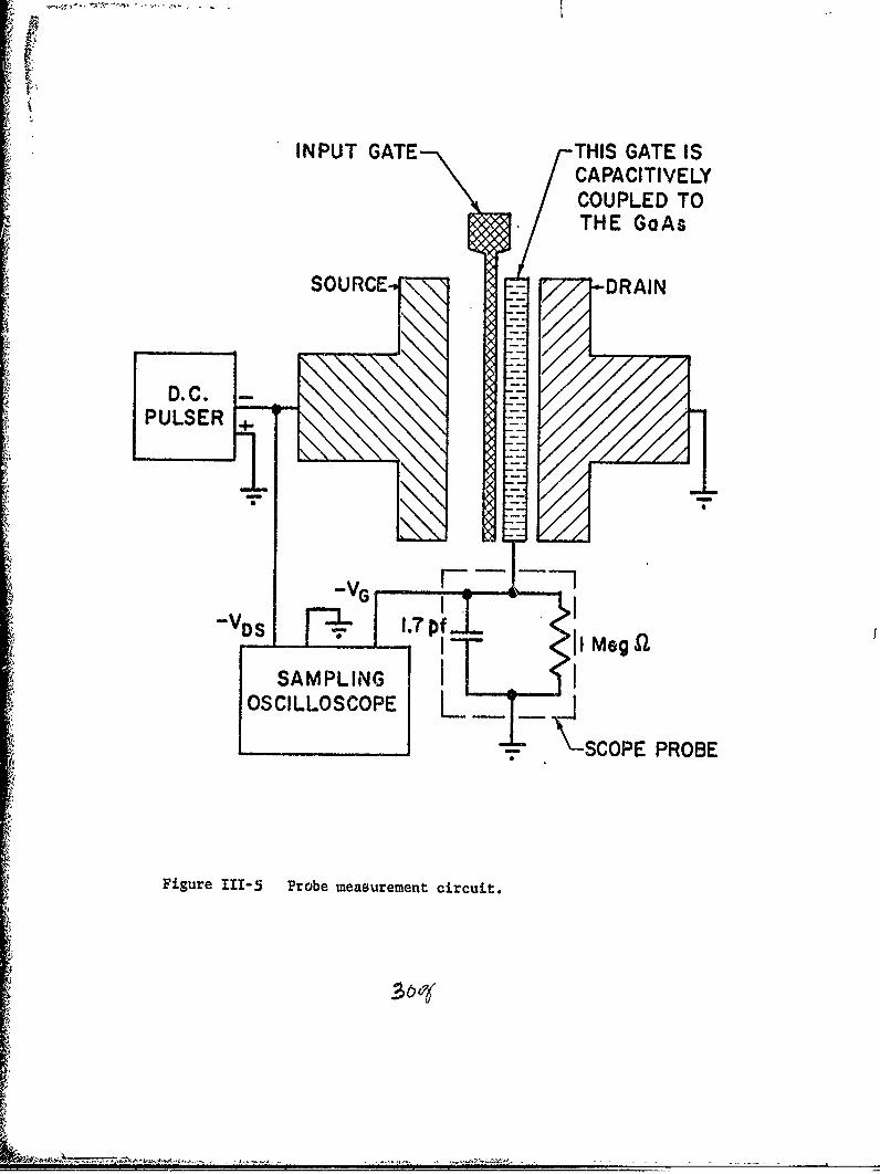
the dc field distribution along the devices. To do this, we mounted an
electrically etched tunsten filament onto the tip of a high-impedance
oscilloscope probc. The probe impedance is 1 megohm in parallel with
1.7 pfarad. The tungsten filament is about 10 A in diameter and it is
bent into the shape of a hook. By using a micropositioner we lowered
20
this filament onto the large gate of the device. Both gates were al-
lowed to float. We then fed the drain-source contacts with dc pulses,
200 nsec in width. The circuit is shown in Figure 111-5. Because both
gates are insulated from the GaAs layer by SiO2 , we relied upon the ca-
pacitive coupling between the epitaxial layer and the large gate to pro-
vide us with a direct measuremunt of the average potential of the epi-
taxial layer immediately below the large gate.
In the first experiments we foiwd that the capacitance to the sur-
rounding epitaxial GaAs of the pad attached to the large gate was short-
ing out our signal, so we carefully scratched away the connection be-
tween the pad and the gate at the position labeled 'A" in Figure 111-2.
This result implied also that the large pad on the rf input gate would
short out in the rf input signal. So, in the subsequent device design
of batch III we have drastically reduced the pad size and in other de-
vices will etch away the semiconductor layer beneath the pad.
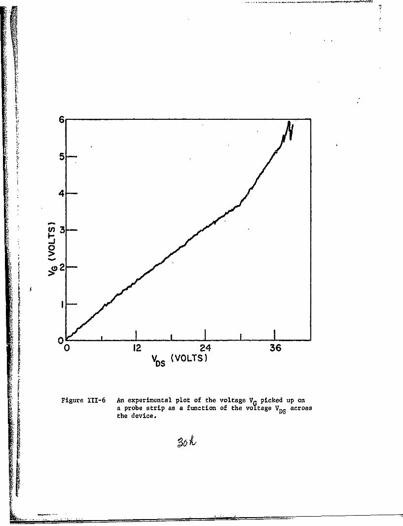
Returning to Figure III-1, it is evident that most of the potential
drop above the threshold potential will be developed very near the drain.
If we consider the drain-to-source voltage Vds vs. the drain-to-gate vol-
tage VG, we would expect that for Vds below the threshold voltage VT, a
curve of Vds vs. V Gwould be a straight line. However, as Vds exceeds
the threshold VT, the curve should slope sharply upward because all the
additional voltage drop appearing across the device will occur between
the grounded gate and the drain.
In Figure 111-6 we show a plot of the value of VG measured on the
probe vs. Vds taken with the circuit shown in Figure 111-5. It will be
noted that the curve does, indeed, double its slope for Vds >VT Z30
volts. This indicates, as expected, that most of the potential drop is
near the drain electrode, and that a better means of controlling the
21
field variation along the device is needed.
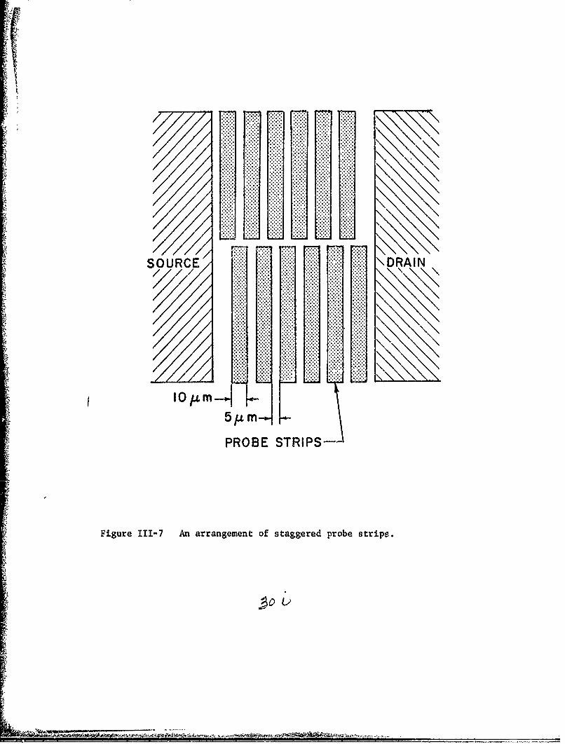
To utilize the same technique to extract more detailed knowledge of
the field along a device, we have made a photolithographic mask which
will be used to deposit a series of narrow insulated gates in the region
between the source and drain. A diagram of the configuration is shown
in Figure 111-7. This configuration will allow us to probe the poten-
tials at several positions along the device.
We are also working on a moveable probe which will eliminate the
need for vacuum deposition of gates on the device's surface. Such a
probe will allow us to measure the dc potential at any point along any
diode at will. We have added one other improvement to our probe which
should allow much more accurate potential readings: we have very care-
fully constructed a stainless steel tip which surrounds the tungsten
- and very effectively shields it from the leads which go to the source
and the drain, eliminating pick-up from the bias circuitry.
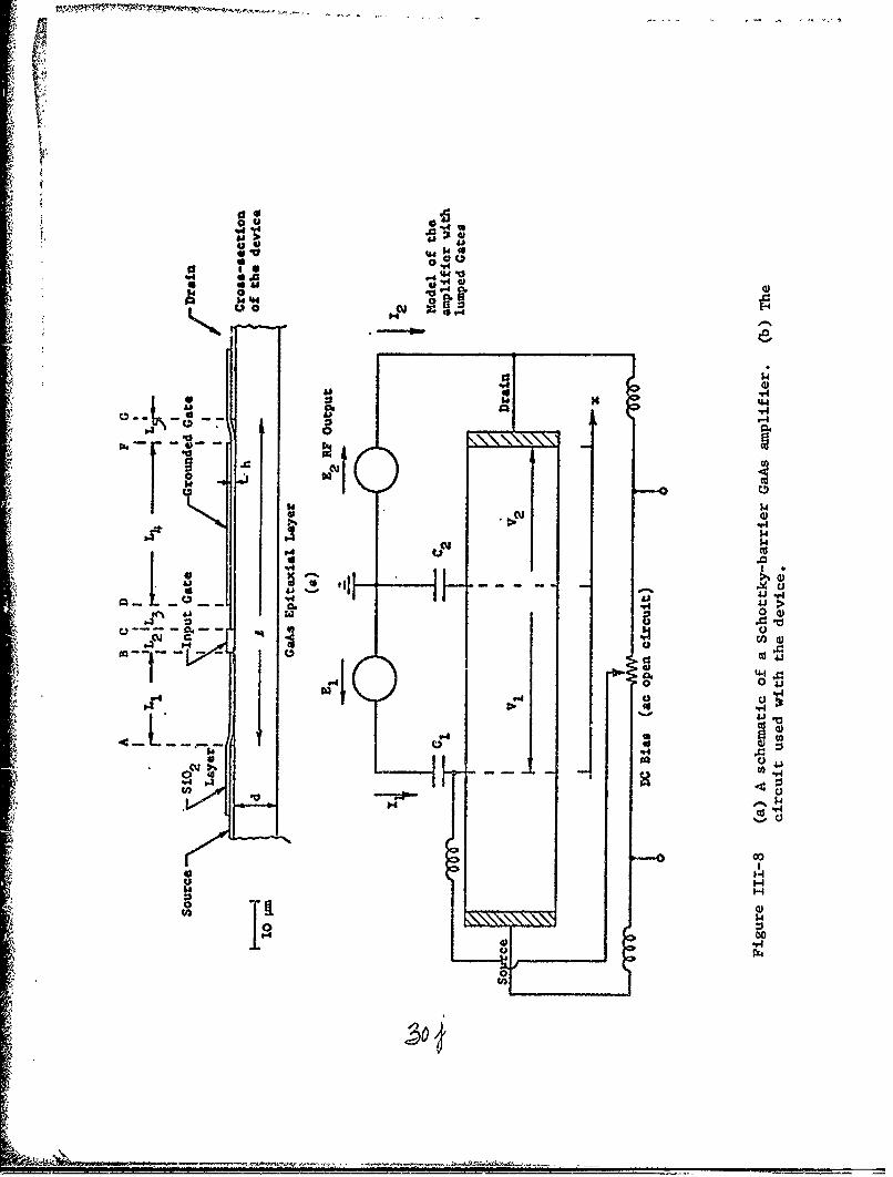
In the previous report we suggested that one way of controlling the
dc field distribution along a device would be to use a back-biased
Schottky-barrier as an input rf gate. A longitudinal view and the asso-
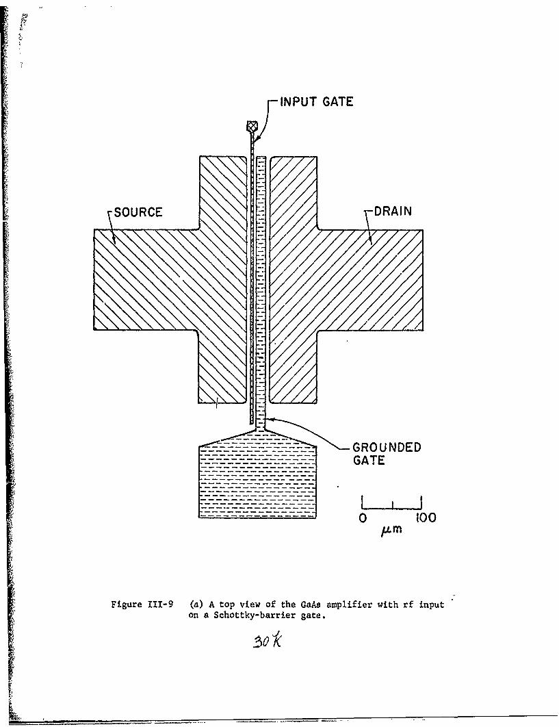
ciated circuitry of such a device are shown in Figure 111-8. The addi-
tional control of the dc field distribution is obtained with the ad-
justable dc bias on the rf input gate. During this present reporting
period we have designed and built a batch of such Schottky-barrier ampli-
fier3 incorporating a much-reduced pad size on the rf input gate. A
schematic diagram and an actual photo are shown in Figure 111-9. In
this latest design, the gap between ohmic contacts is 35 /m. The input gate
is 5 Mm long and has a small pad to reduce the capacitive coupling to
ground. The grounded gate is 15 1m long and the SiO2 layer is 5,000
22
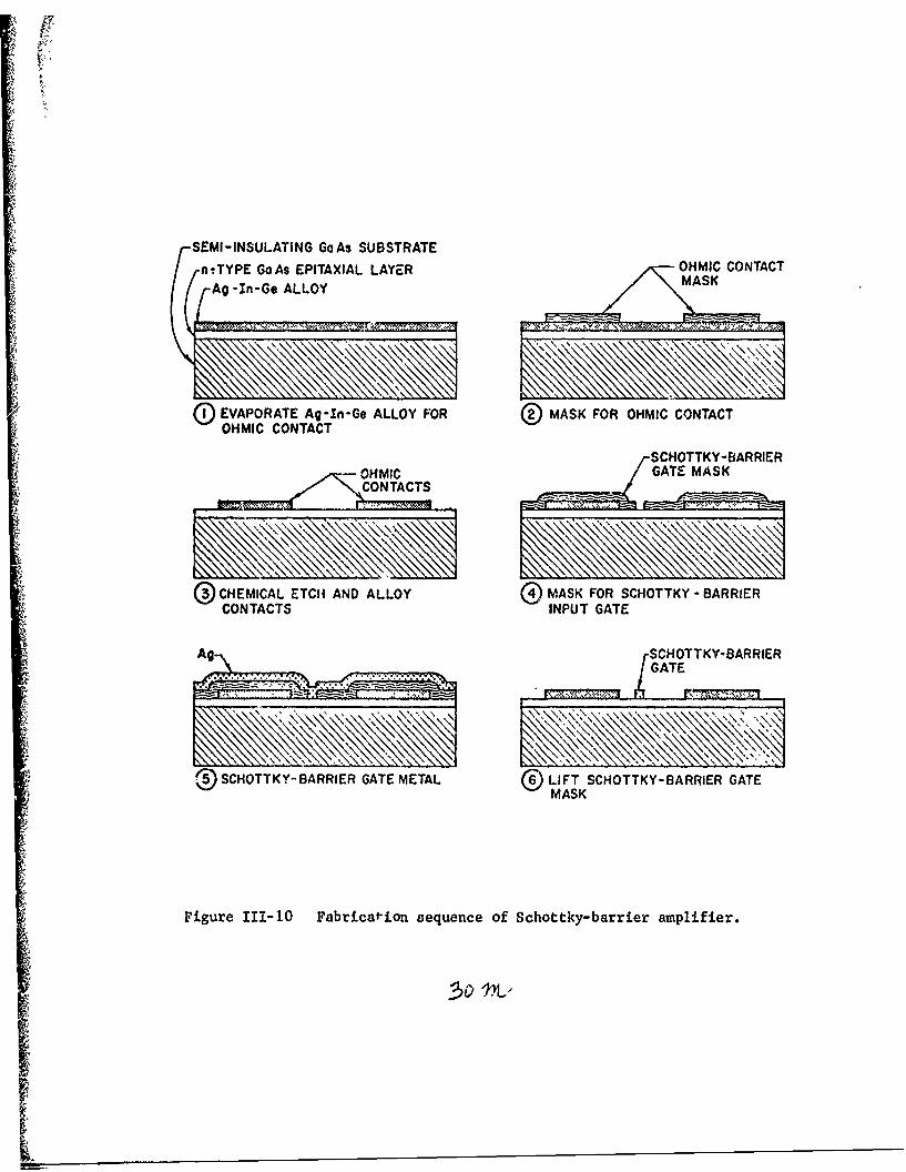
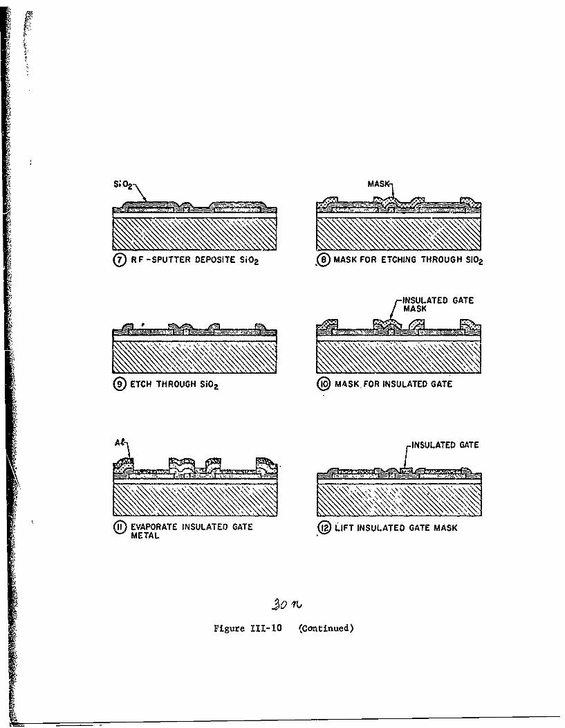
thick. Figure III-10 indicates the fabrication sequences of a h bitch of
such devices. We hope to test these amplifiers in the near future,
pending the construction of new input circuitry-and mechanical mounting
to the Schottky barrier input gate.
We are presently carrying out experiments on etching techniques to
remove the GaAs semiconducting layer from underneath the pad region.
This appears to be a controllable process , so that we should, in the
next set of devices, be able to obtain reasonable size pads to which
we can bond gold wires, without undue problems with the pad capacity.
2. Linear Acoustic Amplifiers
In our last report we showed that appreciable electronic gain was
possible using GaAs as an acoustoelectric amplification medium for a
particular type of surface wave, the Bleustein mode. Following these
results, our main objective in this area has been to improve the acoustic
transducer coupling so that an overall device gain can be achieved for
the amplifier. Additional work has also been done on a comparison of the
amplification characteristics of another type of surface wave, the Ray-
leigh mode.
There are two methods we have been considering for improving the
transducer efficiencies. The most prormising at this stage relies on a
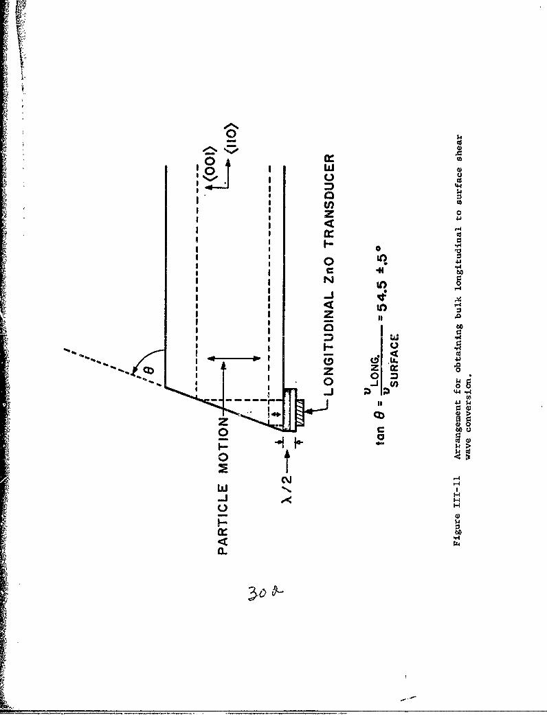
volume longitudinal wave to surface shear wave conversion at a reflect-
ing boundary using the configuration shown in Figure III-11. The angle
of the boundary is chosen so that the phase velocit~es of the two waves
match. The launching transducer employed is a ZnO thin film which, with
present technology, is readily capable of conversion efficiencies in the
range of 15 dB. This compares with conversion efficiencies of 25-30 dB
23
C
for typical interdigital transducers which have been employed in earlier
investigations.
At the output end of the amplifier, the surface shear wave is recon-
verted by a similar mode conversion back to a longitudinal wave for de-
tection. Our study to the present on this transducer configuration has
been with 02 doped GaAs in the form of platelets 0.020" thick. In view
of the small cross-section of the drystal we expect a surface shear-type
wave to propagate along the length. A second advantageous property of
ZnO transducers is the extremely large bandwidth (Q200 MHz) available.
So far, the basic principle of mode conversion outlined above has been
demonstrated experimentally and further investigations are proceeding to
establish the amplification properties of the structure.
Another technique for improving the transducer coupling efficiency
makes use of thin layers of a good piezoelectric material deposited on
the semiconductor surface. This approach is essentially the inverse of
earlier surface wave amplifier structures where one used a good piezoelec-
tric substrate and superimposed a semiconducting film. Our work using
this method is at a preliminary stage, although other investigations 1
have indicated promising results at frequencies below 100 MHz.
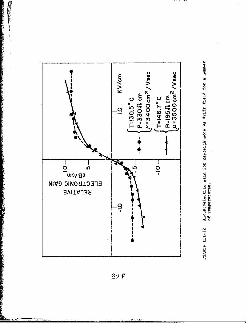
We have pointed out that the amplification characteristics of the
surface shear, or Bleustein wave, come from its deep penetration depth
and from the particle motion being essentially the same as the strongly
coupled bulk shear wave propagating in the <110> direction. Along the
same direction of propagation, but instead on the (001) surface, it is
possible to excite a pure Rayleigh wave which by contrast has two pax-
ticle motions. We have investigated the amplification characteristics of
this Rayleigh wave mode on material similar to that used for the Bleustein
24
wave device and from Figure 111-12 it is apparent that a smaller amplifi-
cation is obtained for this case. The approach used for the measurement
of Rayleigh wave amplification was similar to that used previously,
where the temperature of the sample was adjusted to produce the carrier
concentration yielding maximum gain. The lower gain obtained for the
Rayleigh wave is partly due to the weaker coupling of this mode to the
longitudinal drift field, but it is also due to the greater sensitivity
of this mode to sample homogeneity and surface imperfections since most of
the acoustic fields are confinod to a narrow region just below the sur-
face.
3. Nonlinear Interaction of Surface Waves on GaAs
There has been considerable interest recently in mechanismns pro-
ducing nonlinear interactions of both acnustic surface and bulk waves
in piezoelectric crystals. Much of the effort in this area has been
largely to isolate suitable materials and structures for application to
various signal processing schemes, such as real time convolution, which
can be conveniently achieved through acoustic wave interactions. Among
the interactions which have been reported are the direct acoustic non-
linearity2'3 arising out of departures from Hooke's law at large strains,
and also interactions 4' 5 produced by the presence of carriers in a piezo-
electric semiconductor. Other approaches 6 have involved placing a semi-
conductor near the surface of a strong piezoelectric, where again the
main source of nonlinear interaction occurs from the carriers in the
semiconductor.
In the following we present some results on nonlinear coupling pro-
cesses which occur for surface waves in GaAs. Such interactions have
25
been observed both for surface shear waves on bulk material and for Ray-
leigh waves on epitaxial material. It has been found necessary to intro-
duce different processes to describe the coupling for the two cases, but
for both situations the nonlinear coefficient for the same internal
acoustic power level has been demonstrated to be around 30 dB greater
than for the more strongly piezoelectric materials, such as LiNbO3 ' where
the nonlinear effect results from large strains.
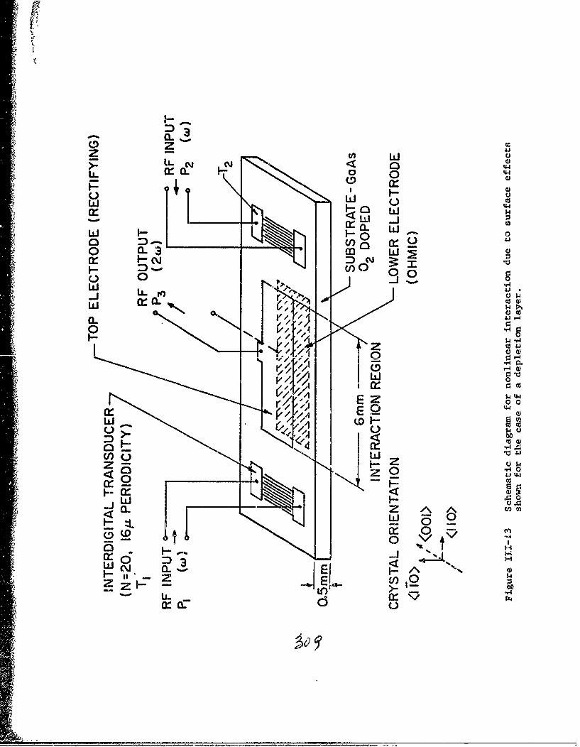
Nonlinear Interaction of Surface Shear (Bleustein) Wavas in GaAs
The configuration for studying the nonlinear interaction is shown
in Figure 1II-13. Surface waves which Ere launched at either end of the
crystal are allowed to interact in the central region between the two
electrodes across the semiconductor. The lower contact is ohmic while
the upper consists of a Schottky barrier contact. The material used in
these investigations was 02 doped GaAs with room temperature resistivity
of 222 ohm cm. The convolution signal is detected on the center elec-
trode at the second harmonic frequency.. The nonlinear interaction
strength is measured by using two oppositely traveling pulses which both
have the same width as the detecting electrode. The convolution output
in this case has a triangular form and the peak value is used to deter-
mine the nonlinear figure of merit. We refer to two definitions of fig-
ure of merit. One is based7 on overall device quantities which are the
actual electrical input and output powers:
p3 -l -2K w cme
where P1, P2, P3 are the electrical powers at the device terminals and
eis the length of the interaction region. It is also useful to have a
26
26
definition which is not dependent on the input transducer efficiency or
propagation loss and we call this the electrcacoustic figure of merit:
P3 -l -2K = w cmea Pa Pa.P1 P2
where P is still the electrical output power but P a P2a are the
32
acoustic powers in the crystal.
The cunvolution property has been checked over a 25 dB range and
has been fcund to be quit,- linear (± 0.2 dB), P3 ranging linearly with
P1 and P No saturation was observed up to acoustic power levels of
1 mw, the current limit due to interdigital transducer efficiency. The
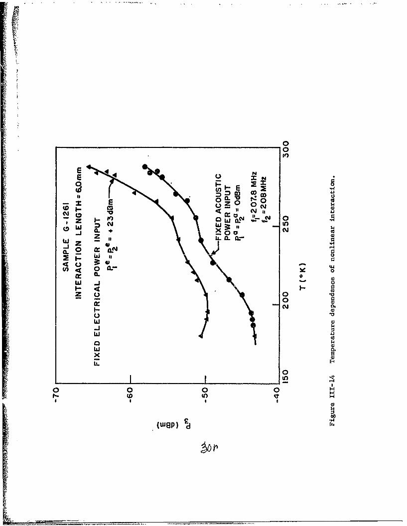
electrical output power P3 showed a strong dependence on temperature as
the sample was cooled but a broad maximum occurred at low tempera tares.
This effect shown in Figure 111-14 has been determined for fixed elec-
trical and acoustic powers into the device, where the latter is obtained
by allowing Aor the variation of the transducer and propagation losseS.
The details of this characteristic are not yet clearly understood, but
it is associated with the rapidly varying carrier concentration.
The convolution signal is not symmetrical with respect to the dc
bias applied to the detecting electrode. For the low carrier concentra-
tions and high trap densities in the material used for these devices
there was no consistent behavior of the convolution signal with dc bias.
In one case it was found that in the forward bias direction the signal
increased while in the reverse direction the signal initially increased
but then decreased with increasing bias. In another, tne signal de-
creased in the forward direction but increase'l in the reverse direction.
These effects may be attributed to a variation of the zero bias depletion
27
layer thickness in relation to the potential associated with the surface
wave. The position of the zero field depletion layer is a function of
the carrier density and can be strongly influenced by traps. 8
Nonlinoar Interaction of Rayleigh Waves in Epitaxial GaAs
One of the difficulties in interpreting fully the surface shear wave
interaction has been due to the high level of trapping in the bulk 02
doped material which makes the initial depletion layer conditions uncer-
tain. The use of an epitaxial layer on a semi-insulating substrate, how-
ever, provides an ideal situttion for studying the Rayleigh wave interac-
tions since their penetration depth is so small. Here it is possible to
use material with a fairly high carrier concentration (2x105 cm-3 ) and
-since the layer thickness is only a small fraction of an acoustic wave-
length, there is negligible attenuation produced.
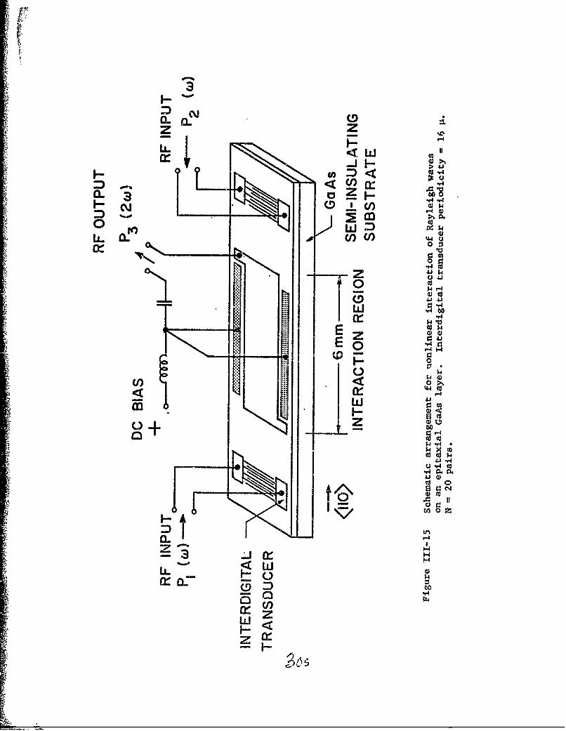
The structure we have used for studying the nonlinear interactions
of Rayleigh waves is shown in Figure 111-15. The center plate is again
a Schottky barrier, but the ohmic contacts in this case run parallel to
the plate along the propagation direction. In the transverse dimension
we have then essentially a field effect arrangement. We view the surface
wave coupling in tVis situation as originating from the basic nonlinearity
of the field effe'.ct structure when the active layer under the reverse
biased Schottky barrier contact is biased into and out of the pinch-off
region. The material used in these experiments was n-'type GaAs with
carrier concentration 2x105 cm-3 and layer thickness of 3-5 A which is
well within the capability of the CMR growth facility.
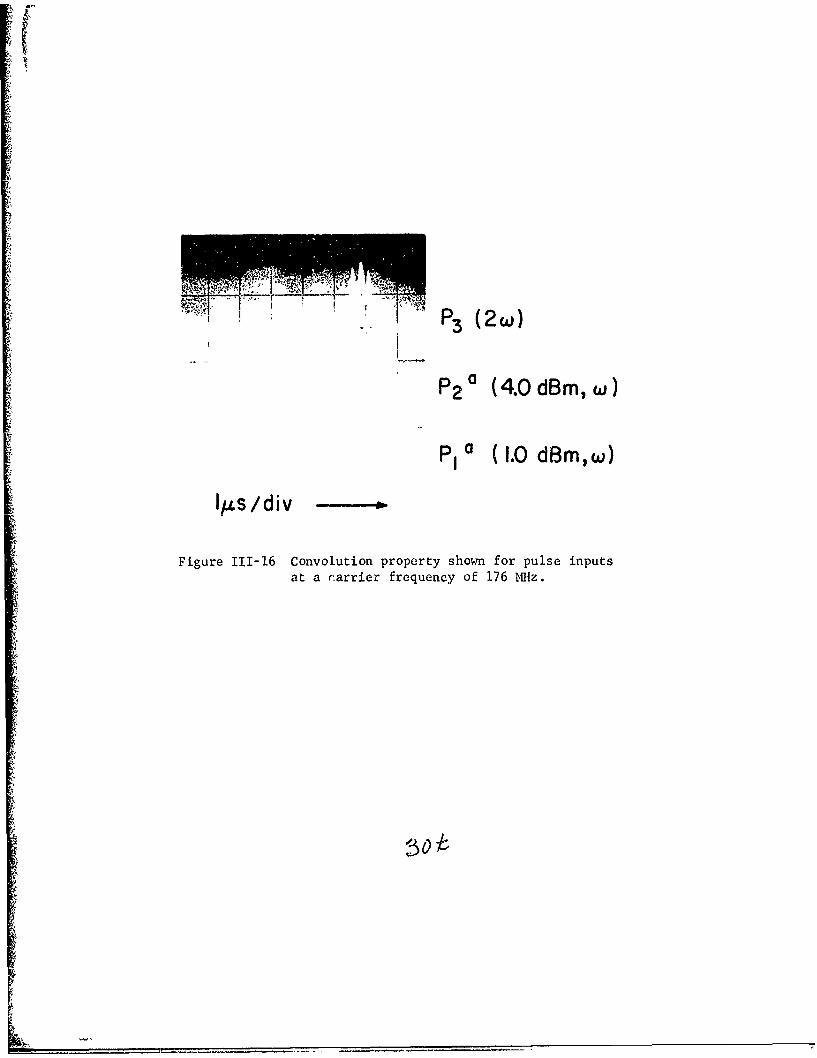
The convolution property of the epitaxial configuration is shown in
Figure 111-16. The input signals are at a fundamental carrier frequency
I28
of 176 MHz and a dc bias has been applied between the contacts to maxi-
mize the nonlinearity. For various combinations of input pulses the con-
volution property was found to be satisfied.
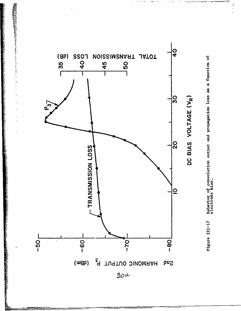
The dependence of the convolution output on reverse bias applied to
the electrodes is shown in Figure 111-17. The maximum output occurs
when tile active layer is almost compl:jtely depleted. There is a corres-
pondence between this point and the point of maximum second harmonic
generation when the center plate is used as L. simple diode and an external
voltage Pource is applied to it, around the same frequency as the surface
waves. In the latter case the second harmonic is monitored by a small
resistance ia series with the diode.
In Figure 111-17 the behavior of the total prope'gtion loss is also
shown as a function of bias, and it is possible to sk.parate out the vari-
ation in this loss from that of the nonlinear interaction. The loss is
found to decrease with reverse bias and become almost constant at larga
bias. The latter effect is attributed to an increase in transducer ef-
ficiency as the epitaxial layer beneath each transducer is depleted of
carriers. Similar observations have been reported on bulk material by
Takeda et al. We note that over the region where strongest nonlinearity
"is observed, the propagation loss changes by only a small amount.
From the work outlined above there is clear evidence for the value
if GaAs in both bulk and epitaxial acoustic devices. For the linear
amplifier configuration we have proposed, it appears likely that reali-
zation of a large bandwidth amplifier with relatively low dc power dis-
sipation should be possible. Further investigation of the amplifier is,
however, still required to achieve the advantage inherent in using an
epitaxial layer structure with mode conversion transducers.
29
For the nonlinear surface wave interaction devices the merits in
making use of the large nonlinearities associated with the free carrier
interaction in an epitaxial structure have been clearly established.
For both types of surface waves on GaAs structures the observed nonlinear
coefficient is approximately 30 db greater than for the more strongly
piezoelectric materials, such as LiNbO3 , where the nonlinearity arises
from large strains. It is felt that practical signal processing de-
vices based on this concept will emerge in the future.
REFERENCES
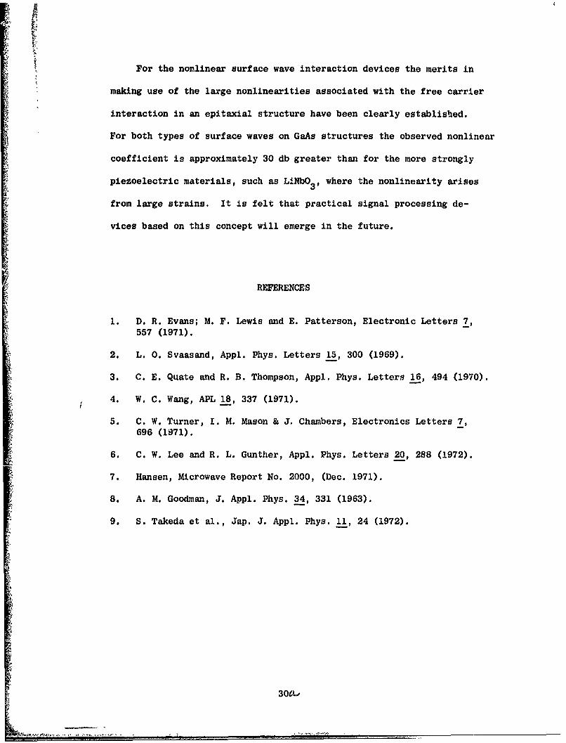
1. D. R. Evans; M. F. Lewis and E. Patterson, Electronic Letters 7,
557 (1971).
2. L. 0. Svaasand, Appl. Phys. Letters 15, 300 (1969).
3. C. E. Quate and R. B. Thompson, Appl. Phys. Letters 16, 494 (1970).
4. W. C. Wang, APL 18, 337 (1971).
5. C. W. Turner, I. M. Mason & J. Chambers, Electronics Letters 7,696 (1971).
6. C. W. Lee and R. L. Gunther, Appl. Phys. Letters 20, 288 (1972).
7. Hansen, Microwave Report No. 2000, (Dec. 1971).
8. A. M. Goodman, J. Appl. Phys. 34, 331 (1963).
9. S. Takeda et al., Jap. J. Appl. Phys. 11, 24 (1972).
300L.,
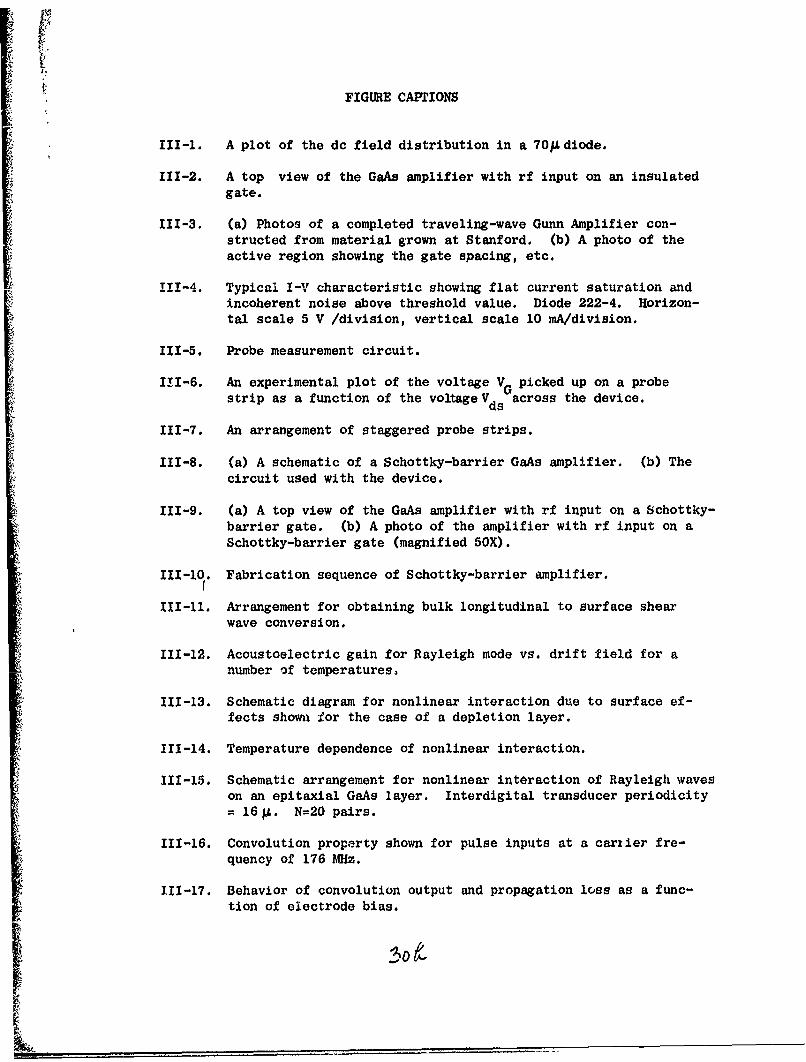
FIGURE CAPTIONS
III-1. A plot of the dc field distribution in a 70A diode.
111-2. A top view of the GaAs amplifier with rf input on an insulatedgate.
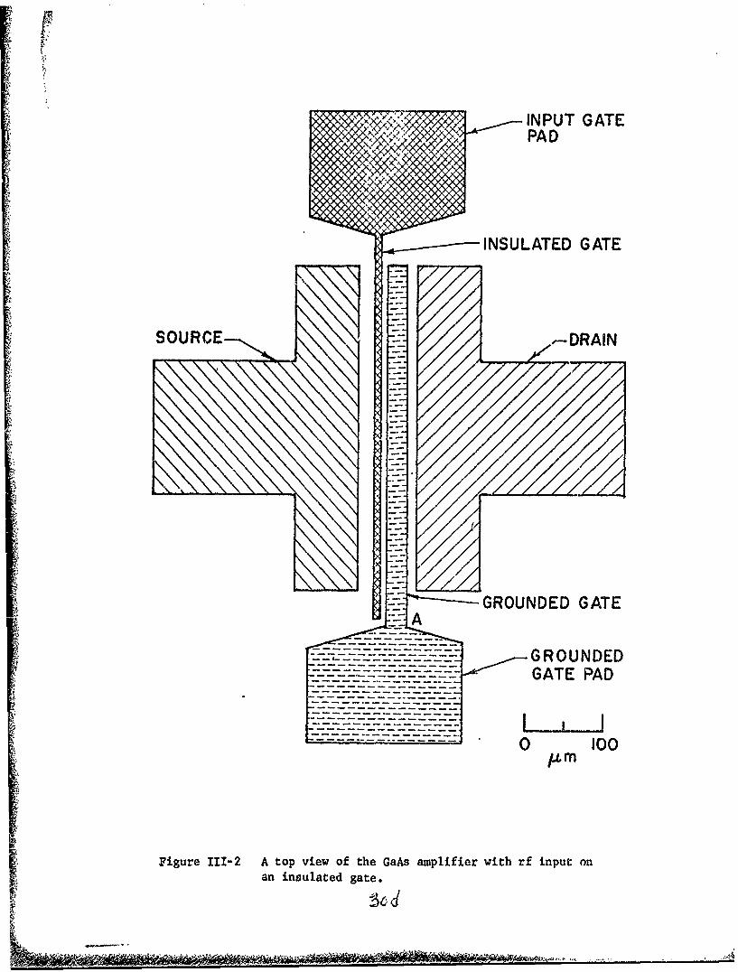
111-3. (a) Photos of a completed traveling-wave Gunn Amplifier con-structed from material grown at Stanford. (b) A photo of theactive region showing the gate spacing, etc.
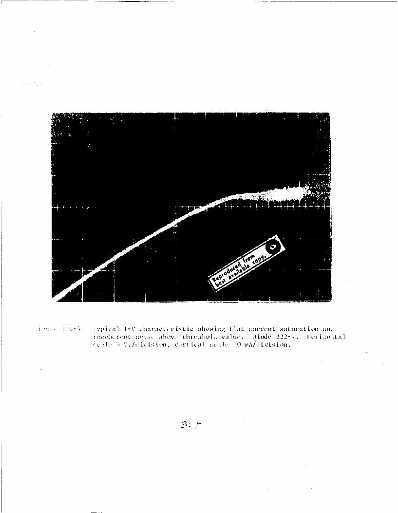
M11-4. Typical I-V characteristic showing flat current saturation andincoherent noise above threshold value. Diode 222-4. Horizon-tal scale 5 V /division, vertical scale 10 mA/division.
111-5. Probe measurement circuit.
111-6. An experimental plot of the voltage VG picked up on a probestrip as a function of the voltage Vds across the device.
111-7. An arrangement of staggered probe strips.
111-8. (a) A schematic of a Schottky-barrier GaAs amplifier. (b) Thecircuit used with the device.
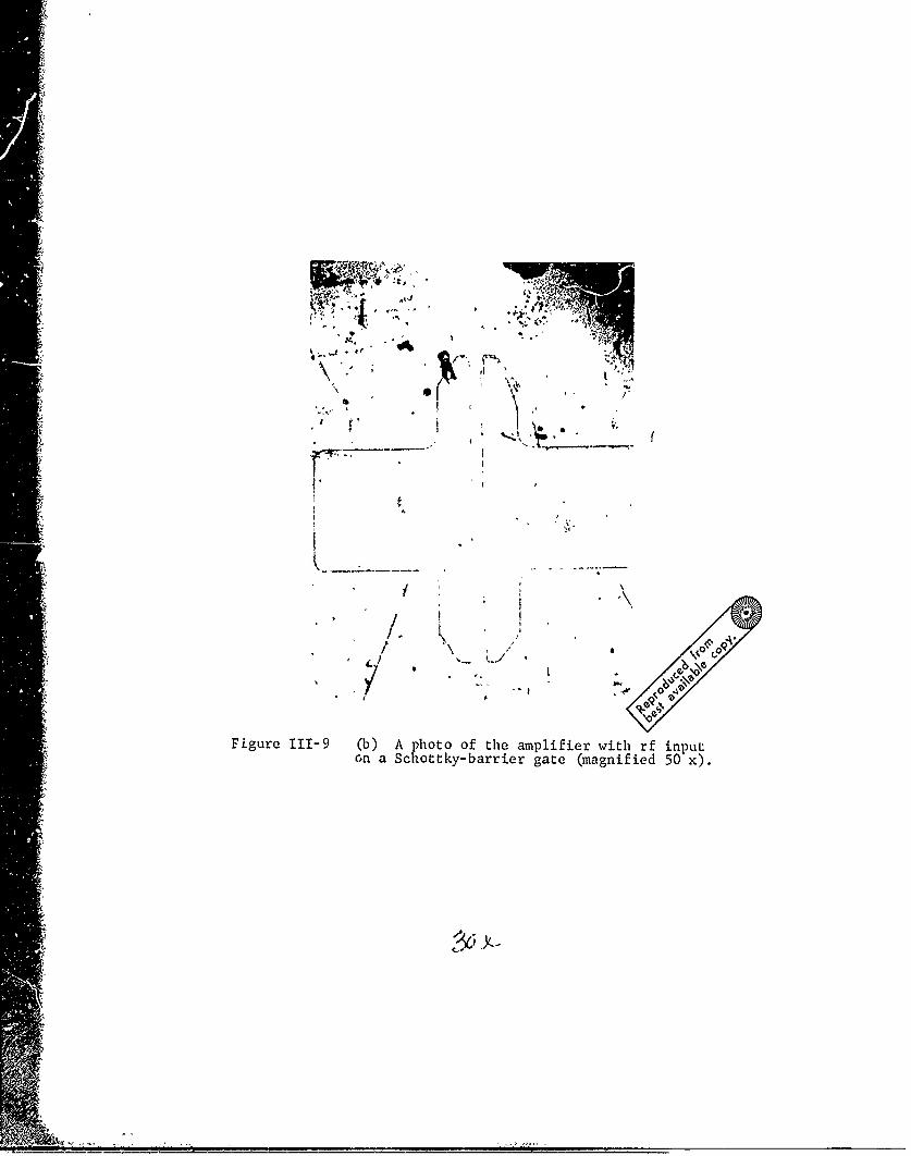
111-9. (a) A top view of the GaAs amplifier with rf input on a Schottky-barrier gate. (b) A photo of the amplifier with rf input on aSchottky-barrier gate (magnified 50X).
III-10. Fabrication sequence of Schottky-barrier amplifier.
III-11. Arrangement for obtaining bulk longitudinal to surface shearwave conversion.
111-12. Acoustoelectric gain for Rayleigh mode vs. drift field for anumber of temperatures.
111-13. Schematic diagram for nonlinear interaction due to surface ef-fects shown lor the case of a depletion layer.
111-14. Temperature dependence of nonlinear interaction.
111-15. Schematic arrangement for nonlinear interaction of Rayleigh waveson an epitaxial GaAs layer. Interdigital transducer periodicity
'- = 161A. N=20 pairs.
111-16. Convolution property shown for pulse inputs at a carxier fre-quency of 176 MHz.
111-17. Behavior of convolution output and propagation loss as a func-tion of electrode bias.
L~
20
18
16
14-
12- v/VT= 2
E/.T -
10-
8 v/VT 1.25
6-SATURATION
4-GAIN IN THIS
2- REGION
2-....- DECAYING WAVE -I0 , I "- I I
0 10 20 30 40 50 60 70DISTANCE IN pum
Figure III-I A plot of the dc field distribution in a 70 p diode.
[ INPUT GATEt PAD
S.__..•---INS U LATED GATE
SOURCE-,, ,-DRAIN
"--"---GROUNDED GATEA
•-- -- •----_-_---- • GROUNDED-------------------- GATE PAD
"- --I --- ----
Figure 111-2 A top view of the GaAs amplifier with rf input onan insulated gate.
3d
--- - -' .-$9-.-C- -
Re,,prodCucedH frornLbest available coy
Figure 111-3 (a) Photos of a completed traveling-wavc. Gunn amplifier constructedfrom material grown at Stanford. (b) A photo of the active regionshowing the gate spacing, etc.
v Ii-. I cI I V c 1 IhlrdciL rLs L Lc 11 OWi111 1Z IaL c uI-rt-11L sa L i IraL L oIl aiidIhiIh tr-cn L noL':, ,Ibov, L~il-c~shoId vaI Va Di)ode' .222-ý 110lri;:.0Inia L
IC V . /d L\, is; it'll vrt ica Isci1 I, 1O iiIA/Ali v i s ill
INPUT GATE THIS GATE ISCAPACITIVELYCOUPLED TOTHE GaAs
SOURCE-, -DRAIN
D. C.-PULSER_.
------ VG
TVDS 1I7eg-V~~~~s • f Imeg a
SAMPLING IIOSCILLOSCOPE L2
SCOPE PROBE
Figure 111-5 Probe measurement circuit.
5-
4
(13
I-
0
00 12 24 36
VD S (VOLTS)
Figure 111-6 An experimental plot of the voltage V picked up ona probe strip as a function of the voltage VDS acrossthe device.
SOURCE ... \DRAIN
10M-] SRP\
PROBE SRP
Figure 111-7 An arrangement of staggered probe stripe.
0.~
00~
u0 0' 4
0 5.4
*9A
- 0
M - - -- .'
".4
5414~~ -'r4
0 .tS 14
'.4 4 4J: r~3"I 4)0. .94 4j5.2'
U--- -0.-
TINPUT GATE
---- ---- ---- GROUNDED----- ---- ---- GATE
__ L LW--- ---- 0---100--
- - - - - - - - -
Fiur 11- () - tp ie o te a- aplfir it r ipuon Shotk- barrier gate
- -- - - -
--- --K- 0V0L____/. __
i *1
- - -4 ; .,
- I
........ (-- _< iur I- b Apooo heapiirwirr nu___@on Sehttk-bariergate(manifid 5 3)
_ - . - .
4 rv
SEMI-INSULATING GaAs SUBSTRATE
n-TYPE GaAs EPITAXIAL LAYER OHMIC CONTACTAg-In-Ge ALLOY
.. ,, AF.,°
EVAPORATE Ag-In-Ge ALLOY FOR @MASK FOR OHMIC CONTACT
OHMIC CONTACT
SCHOTTKY-BARRIEROHMICGATE MASK
•,• \CONTACTS
CHEMICAL ETCH AND ALLOY MASK FOR SCHOTTKY - BARRIERCONTACTS INPUT GATE
Ag_ý SCHOTT KY- BARRIERGATE
SCHOTTKY- BARRIER GATE METAL 0 LIFT SCHOTTKY-BARRIER GATEMASK
Figure III-10 Fabricat-ion sequence of Schottky-barrier amplifier.
i 3o . ,
RF -SPUTTER DEPOSITE SiOp MASK FOR ETCHING THROUGH S10
rINSULATED GATE
ETCH THROUGH SiO2 MASK. FOR INSULATED GATE
At INSULATED GATE
0EVAPORATE INSULATED GATE LIFT INSULATED GATE MASKME TAL
Figure III-10 (continued)
Ifd
0014
00
41)I-44U. 0
Ul)
-p4
00
I I I1-4
I Z 44CL 8
E E E0 4
U') 0
0)
C1*4t-
o c~1-4.9~1-4
Of4~t3. :2~2n SW
-SO -P ~ ~ '
0 40
LL 0r a. 4-4
(LC)
w 0 0
w.~ .q JF- 0 0
0 -0
L.f4
"r4I...,f'
00
1444
E Z .00
r 44J
cr14-
0
w C4 --J. a. Z En 0
<S )
10
EN
a' a. o r0EE L) Z0 c'J'.
CL0im t)
CLx '.4
W z
4c.40 0
w - 0Z 0
-00
'.4
wo 5.4
0)w 0x
0I t1t
o 0 00H00
boC A(wep) '
zz .
z- -
fr.
00
0:0
E 0 0
~44z '-W
0 J Zo-r -
44
0 "44L 924
- ~ *14
zr
-H4
P3)
P2 a (4.0 dBm, w)
PI a (1.0 dBm, w)
Ijis/div
Figure 111-16 Convolution property shown for pulse inputsat a carrier frequency of 176 Mltz.
00
U) 0 in) 0
0
ocro 0
00 0
F-4
U)N 04.,
0 :0
J 0
00
r14
2~ ow
00
r-4
0 0 0j
(wJGP) d J..fdin O INO~WVH PUZ
IV. PRECIPITATION STUDIES IN COMPOUND SEMICONDUCTORSD. A. Stevenson and W. C. Rhines
A. PROGRAM OBJECTIVES
The occurrence of precipitationin compound semiconductors is of
practical interest because of the influence on the electrical and optical
properties. The precipitation of electrically active foreign atoms may
cause a disparity between the bulk concentration of foreign atoms and
the concentration of foreign atoms that are in solution. If local dis-
tortion of the lattice accompanies precipitation, then changes in dis-
location density may accompany the precipitation process. In addition,
the mere presence of a dispersed precipitate will modify the electrical
transport and optical properties of semiconductors. The question of the
extent of precipitation, the nature of the precipitate and the mechanism
of precipitation are questions of practical relevance.
Precipitation in zinc vapor-doped GaAs has been the major topic of
study to date and was selected because of its relevance to devices and
the conflicting reports in tho literature on the characteristics and
identity of precipitates in this system. The major emphasis in this
study has been the use of transmission electron microscopy. The progress
in the report period is described below.
B. PROGRESS
During the report period, the major portion of the experimental work
on precipitation caused by Zn diffusion in GaAs has been completed and
analysis is now in progress. Data have provided the first correlations
between actual observation of precipitates and the variables of diffusion
time, temperature, source, quench rate, and starting material. Although
31
no positive identification of the precipitates has bsen possible, experi-
mental results indicate that it is formed by an isothermal, internal re-
action of Zn with an unknown impurity in the GaAs.
1. Effect of Variables
The following general trends were observed concerning the influence
of diffusion variables upon the precipitation process: (1) as time at
the diffusion temperature increases, the precipitates show a slight size
increase and a greater tendency toward faceting, as opposed to the pre-
dominant strain fields for short diffusion times; (2) increases in dif-
fusion temperature from 700 through 900 0 C cause the precipitate size to
increase. Precipitates in the high temperature diffusions are faceted
while, at lower temperatures, they show distinct strain fields. Pre-
cipitate distribution is relatively uniform at high temperatures. At
lower temperatures precipitates are isolated in linear patterns, mostly
along dislocations; (3) precipitate character shows very little varia-
tion as the quantity of pure Zn in the diffusion source varies. The
Zn+As diffusion source partially suppresses precipitation and decreases
the rate of Zn diffusion; (4) undoped and Te-doped GaAs show identical
precipitate distribution and size when diffused with Zn. Zn melt-doped
GaAs (5xl018 cm-3 ), when further diffUsed from a pure Zn source, shows a
smaller number and size of precipitates than the undoped or Te-doped
starting material; (5) rate of quench has very littie effect on precipi-
tates. Very rapidly quenched samples show enhanced strain fields, while
slowly cooled samples are highly faceted.
2. Identification Attempts
Reflection electron diffraction was performed in the transmission
32
electron microscope on a variety of diffused samples. Diffraction from
a second phase precipitate could not be detected. Several types of ex-
traction replicas were prepared from cleaved cross-sections of diffused
samples. Possible precipitates were observed in some cases, but no dif-
fraction spots could be found. The scanning electron microscope was
also used to observe cleaved cross-sections with little success. Dif-
ferential thermal analysis showed no peaks characteristic of a second
phase. Guinier de Wolff X-ray diffraction revealed two reflections from
the precipitate phase. The reflections are not characteristic of any
known compound or phase formed from Ga, As, and Zn, nor are they promi-
nent reflections of any known Zn compound. Mass spectrographic analysis
of Zn-diffused GaAs showed 26 ppm oxygen. Samples of oxygen-doped GaAs
(10 18/cm 3) were, therefore, diffused with Zn and examined in the trans-
mission electron microscope. Only a few very small precipitates were
observed.
3. Hot Stage Electron Microscopy
Samples containing precipitates were heated to 7860 C in the electron
microscope and held for over two hours. Strain fields relaxed but no
significant dissolution of the precipitates in the GaAs matrix occurred.
This confirms the igothermal formation of precipitates at the diffusion
temperature and strongly suggests an internal reaction of Zn with an un-
known impurity.
Hot stage electron microscopy of GaAs is limited by the vaporiza-
tion of As from the sample surface which destroys the polished surface
and makes examination impossible after several hours at 8000 C. Diffusion
of Zn into GaAs was attempted in the microscope by preparing thin samples
of GaAs with rf sputtered layers of Zn followed by SiO2 on both surfaces.
33
Lattice deformation of the GaAs caused spalling of the SiO2 and prevented
transmission examination after a few hours at 800 C.
4. Deformation of Zn Melt-Doped GaAs
Heavily Zn melt-doped samples of GaAs were deformed at 800 0C to see
if precipitation would occur. Extensive dislocation tangles were seen
by transmission electron microscopy but no evidence of precipitation ap-
peared.
5. Ion Implantation
A proton-assisted diffusion of Zn into GaAs was conducted to see if
appreciable Zn penetration and concentrations could be achieved by dif-0
fusion at lower temperatures. Samples with 100 A thick, rf sputtered
layers of Zn on the surface were heated to 5000 C while bombarding with
"W 1 5 2 ' c evidence of precipitation or dislocation damage was
seen in the samples.
C. FUTfURE PLANS
In addition to analysis of the data on Zn-doped GaAs, the followirg
studies are planned:
(1) Electron microscopy of vapor and liquid phase epitaxial layers
of GaAs and GaAsxPl1x before and after diffusion.
(2) Electron microscopy of doped GaN epitaxial layers, thinned by
ion bombardment.
(3) Electron microscopy of epitaxial Ga xAl 1xAs to detect chemical
inhomogeneities.
(4) Proton-assisted diffusions of Zn into GaAs at a variety of
temperatures, followed by electron microscopy.
34
(5) Furt.er ternary diffusion path determinatioi~s in the Ga,-As-Zn
system.
(6) Electron microscopy of Zi%,.diffused GaP to study precipitation.
3
4-
3S
V. RELATIONS BETWEEN DISLOCATIONS AND MECHANICAL PROPERTIES AND THEPRODLCTION AND CHARACTERIZATION OF DEFECT STRUCTURES IN COMPOUNDSEMICONDUCTORSR. H. Bube, W. D. Nix, B. Liebert and A. L. Lin
A. PROGRAM OBJECTIVE
In this part of the research program we are attempting to devise
techniques for modifying and characterizing the line defect structures
in compound semiconductors, particularly GaAs, through high temperature
mechanical deformation. The objectives of this work are to discover and
understand the effects of various types of dislocations and dislocation
arrays on the important electrical and op'o-electronic properties of
GaAs and to suggest ways of utilizing dislocations in devices. Our
present work on GaAs is motivated by the extensive microwave device re-
search on this material at Stanford. It is expected that our work will
contribute to the device research and to the related crystal growing ef-
fort by providing basic information about the effect of dislocations in
these crystals.
B. PROGRESS: Pure GaAs
In the previous progress report it was mentioned that the effects
of dislocations on the carrier concentration should not be manifested
until p/b, the dislocation density divided by the Burgers vector, was
approximately equal to or greater than the carrier concentration. Since
there exists a physical limitation on the density of dislocations that
may be introduced, the only parameter than can ba varied is the carrier
concentration. Ior our experimental conditione it is necessary to have
a carrier concentration of 1014 cm or below to observe the intrinsic
effects of dislocations. However, we are not able to obtain bulk GaAs
36
crystals of this purity. It would be possible for us to carry out the
bending experiment on epi-layered crystals so long as the substrate is
insulating and the epi-layer has a sufficiently low carrier concentra-
tion. We have attempted to obtain such material commercially, without
sccess and some effort has been made by the Crystal Growing Group to
prepare the epi-layers for our experiment, but as yet we have no results
to report.
Because we have not yet obtained GaAs with a sufficiently low car-
rier concentration, we have been faced with two alternatives. We could
drop gallium arsenide from consideration and begin a study of a different
material, one in which a sufficiently low carrier concentration is readily,
available., e.g., silicon. However, since we have seen changes of car-
rier concentration in our samples after bending, it may be worthwhile to
continue this study of GaAs in an attempt to understand the mechanisms
responsible for these large effects. iuýring the report period wc have
selected the latter alternative.
In order to determine the possible scattering mechanisms before and
after bending, Hall measurements yielding a straight line when mobilhty
is plotted vs. l/T are desirable. An inspection of the mobility curves
in our previous report indicates that low temperature (4?K to 77 0 K)
measurements are therefore necessary. An existing helium system was
modified for the purpose of making Hall measurements and an initial run
(from 77 0 K to 3000 K) was made to check on our ability to reproduce our
previous measurements with this system. A large discrepancy xn both
carrier concentration and mobility was observed (Figures V-1 and V-2).
This may have been due to aging of the sample, poor contacts, or improper
37
functioning of the sample holder and helium dewar. Since no problems
have been encountered with samples or contacts in the past, it is reason-
able to conclude that this large discrepancy must lie with the equipment.
Our present plan is to purchase a new helium system for our laboratory
so that these low temperature measurements can be made. When this
equipment becomes available, this phase of our study of the effects of
plastic deformation on the electrical properties of GaAs will be termi-
nated.
C. PROGRESS: HIGH RESISTIVITY GaAs:Cr
1. Analysis of Photo-Hall Data
Results are presented on three samples of GaAs from the same ingot
and with the same iiitial dark conductivity: (1) an as-grown sample,
(2) a sample heat-treated at 580 0 C for 1 hour, and (3) a sample subjected
to deformation during 50 min. at 5800C after a 10 min. pre-heating, to
produce excess Ga-dislocations by so-called a-bending. Initial results
were reported in the Semi-Annual Report for the period 7/1-12/31/71.
Measurements have been refined and completed, and some analysis of the
results carried out.
Photoconductivity response spectra at 80 0 K in the extrinsic range
are given in Figure V-3, and quantitative data for the intrinsic range
are summarized in Table V-I. Measurements linking the extrinsic and in-
trinsic ranges between 1.2 and 1.5 eV were exceedingly difficult to make.
Time constants exceeding 10 hours in magnitude characterized the attempt
to establish a steady-state in this range after ohotoexcitation in the
range from 1.0 to 1.2 eV. It is likely that at least some of the diffi-
culty car, be attributed to electrode effects, as summarized in a later
38
section.
The photo-Hall mobility as a function of photon energy for these
three samples is given in Figure V-4. Heating introduces new structure
in the range 0.85-1.0 eV, which is retained in the deformed sample. De-
formation lowers the mobility in the intrinsic range.
On the assumption that most of the phenomena observed in Figure V-4
for the Hall mobility is due to two-carrier effects, the conductivity
data of Figure V-3 and the mobility data of Figure V-4 were combined to
permit the caiculation of hole and electron densities. To achieve
numerical values, it is necessary to assume values for the one-carrier
mobilities. Guided by the measured values of mobility in Figure V-4,
we chose a mobility ratio of 10, and electron mobilities of 3400 (as-
grown), 7500 (heated), and 5000 (deformed) cm 2/V-sec, respectively.
Absolute values depend on the actual choice, of course, but relative
variations are not very sensitive. Results of such an analysis for p
and n are given in Figure V-5 for the extrinsic rang6; intrinsic results
are included in Table V-I. Since the measured mobilities are much less
than the assumed electron mobility over most of the spectral range, the
analysis predicts a value of p in excess of that of n. It is not likely
for this actually to be the case in view of the optical quenching pheno-
mena observed, and probably results from variations of effective carrier
mobilities with exciting photon en. rgy and from inhomogeneities in the
crystals; other choices of #/n and /p will 1e made in the future to ar-
rive at a resolution of this question. Such changes in analysis are not
likely to alter the basic variations with photon energy shown in Figure
V-5, or the strong decrease in n in the heated crystals in the quenching
range of 1.0 to 1.5 eV.
39
An initial attempt to begin the descr:'.ption of the detailed photo-
Hall mobility vs. photon energy data of Figure V-4, in terms of the two-
level model generally established for GaAs:Cr, is given in Table V-II.
The numerical data given are for 80°K and the energy values have an un-
certainty of ± 0.02 eV. Within this frar.ework the observed dependence
of A H on photon energy between 0.65 and 0.90 eV can be reasonably corre-
lated. For higher photon energies than those included in Table V-II,
the as-grown crystal appears to behave differently from the heated and
bent crystals. Both of the latter indicate an increase in electron ex-
citation when JXw exceeds 0.90 eV, followed by an increase in hole exci-
tation when X1w exceeds 0.95 eV. Levels lying 0.1 eV below level A and
0.1 eV above level B would formally satisfy this requirement, Allen
(Drit. J. Appl. Phys. 1, 593 (1968)) proposes a possible band of ener-
gies for Cr in GaAs with a width of about 0.1 eV. We shall continue to
explore the best way to interpret the photo-H&'l data.
2. Optical Quenching of Photoconductivity
Measurements of the optical quenching of photoconductivity at 800K
were completed and are compared for the three samples in Figure V-G. The
quenching spectrum consists of a broad structure with minimum energy of
0.90 eV (corresponding to X(j•> 0.85 eV in th& mode] of Table V-II), and
a small auxiliary quenching band witb maximum at 0.8 eV (correspcnding
tn 0.7 oV< 4w< 0.8 eV in the model of Table V-Il).
3. Thermally Stimulated Conductivity
The thermally stimulated conductivity of these tbree samples after
photoexcitation at 80 0K by monochromatic intrinsic or extrinsic radia-
tion is summurized in Figure V-7. Striking structure is found in these
40
TSC curves, which is sensitive in absolute and relative magnitudes to
the processes of heating and deformation. Of perhaps even greater in-
terest is the correlation between the structure reported here for high-
resistivity GaAs:Cr and other reports of high-resolution fine structure
in TSC data on other forms of high-resistivity GaAs. Table V-III com-
pares our data with that of Haisty, measured on undoped high-resistivity
GaAs, and that of Blanc et al., measured on Cu-diffused high-resistivity
GaAs:Cu. The agreement between the peaks found by us and those reported
by Haisty is very close, indicating a real materials property, but
probably not one related to Cr impurity. Estimate of the trap depths
indicates that they probably all lie between 0.19 and 0.42 eV.
Haisty reported strange properties of the TSC peaks in his material,
depeiAdent on time and intensity of photoexcitation. His work was done
with "white" light. Although our data seem well-behaved for monochro-
matic excitation, we also find marked differences if "white" light is
used. Figure V-8 shows the TSC curves obtained after three different in-
tensities of white-light excitation on our deformed sanple (compare
Figure V-7). For the highest intensity, three peaks are found, at 1170
and 130°K (corresponding roughly to the two lowest-temperature peaks in
Figure V-7) and a large peak at 2840K (0.57 eV). A similar deep trep
TSC peak is roported by Haisty for high-intensity long-time vwhite-light
photoexcitation. It is likely that at least some of the strange effects
of white-light excitation are due to the simultaneous excitation and
quenching effects. Long-time phctoexcitation by monochromatic radiation,
which both excites and quenches, was observed for our deformed sample
to decrease the low-temperature TSC peaks ,nd increase the higher-tem-
perature TSC peaks. The dramatic effect of irradiating tha sample with
41
1.08 eV quenching radiation after 0.85 eV exciting radiation is shown by
Curve 4 in Figure V-8; all structure disappears.
4. Deformation to Produce Excess As-Dislocations: O-Bending
Attempts were made to produce 0-bending of the GaAs:Cr crystals, in
order to compare the effects with those reported above for a-bending.
Successful a-bending had been accomplished, as mentioned above, with a
total heating time of 1 hour at 580 0 C with a load of 1.2 kg in the 4-
point bending apparatus.
Four attempts to produce 0-bending all ended in a fractured sample.
Fracture occurred in all cases for a deformation of the crystal con-
siderably less than that produced by 0-bending. The four samples frac-
tured in different locations along the bar and into a different number
of pieces. In each case the fracture occurs (at least macroscopically)
along a 11101 plane. This observation is consistent with other studies
of III-V compounds (M. S. Abrahams and L. Ekstrom, Acta Metall. 8, 654
(1960)). Optical examination of the fracture surfaces revealed "river
patternsI which are indicative of cleavage fracture. A preliminary
study of the river patterns indicates that the cleavage cracks are nu-
cleated on the tension side of the bent sample, as one would expect.
However, this observation will be checked with a more careful study with
the electron microscope.
The observition that thb samples are more brittle when deformed by
0-bending is interesting not only from a mechanical viewpoint, but from
the electronic point of view as well. It is not at all clear why .- dis-
locations should be more effective than a-dislocations in producing frac-
tures. The fact that they :.e (or seem to be) may be indicative of some
42
important structural or electronic differences between the a and 0 dis-
locations. Some insight into this problem can be gained by considering
the work of Abrahams and Ekstrom on cleavage nucleation in covalent ma-
terials. They pointed out that cleavage cracks in elemental semicon-
ductors occur on 1 lll1 planes, in contrast to the 1 101 cleavage for
III-V compounds. They suggested that this difference arises because of
differences in the core structure of Lomer-Cottrell dislocations in
these materials. Briefly, in all solids with the FCC lattice, pairs of
glide dislocations of the type [a <l10> 111 can react to form Lomer-
Cottrell sessile dislocations. These dislocations are edge dislocations
of the type 2<110> 101.Abrahams and Ekstrom showed that all of
the atoms in the core of a Lomer-Cottrell dislocation in a group IV solid
can form covalent bonds (although distorted) with their nearest neigh-
bors. In contrast, the core structure of the Lomer-Cottrell dislocation
in III-V compounds is such that covalent bonding cannot be satisfied.
They suggested that cleavage in III-V compounds occurs on the 1101
planes because it is nucleated on those planes by the stress fields of
the Lomer-Cottrell dislocations. It may be possible to extend this the-
ory to explain the observation that the high resistivity GaAs crystals
are more brittle in #-bending than in a-bending. This extension should
take account of the possible effects of charge on the core structure of
the Lomer-Cottrell dislocations as well as the effects of electric charge
on the intensity of the stress at the point of cleavage (charges on dis-
locations will affect the dislocation distribution in pile-ups). Also,
some consideration should be given to the fact that the brittleness ob-
served for 0-bending of high resistivity GaAs was not observed for con-
ducting GaAs.
43
5. Electrode Effects
As shown clearly in Figures V-3 to V-5, low-temperature photocon-
ductivity measurements on GaAs:Cr involve two-carrier effects. We have
found that the magnitude of the measured probe voltage (i.e., the vol-
tage drop along the crystal measured with a high-impedance voltage de-
tector from two probes along the length of the crystal) is a very good
indicator of the sign of the domxnant carriers for a particular kind of
electrode material. For indium contacts, as used in the results reported
here, the probe voltage is large and normal in the intrinsic range and
for photon energies less than 1.0 eV, but drops to much smaller values
in the intermediate range where p-type photoconductivity is found. For
zinc contacts, the probe voltage is large and normal in the intermediate
range of p-type photoconductivity, but drops to much smaller values in
the intrinsic and low energy ranges. Further investigation of electrode
effects will be reported later.
D. FUTURE WORK: HIGH RESISTIVITY GaAs:Cr
(1) Continued development of a suitable model and interpretation of
the datR in terms of that model.
(2) Exploration of electrode effects and correlation with data in-
terpretation.
(3) Investigation of the effects of heating at different tempera-
tures and for different lengths of time.
(4) Attempts to produce 0-bending without fracture.
(5) Anneal samples after deformation to see effects on photoelec-
tronic properties measured subsequently.
IJ
(6) Start with GaAs:Cr material with lower initial dislocation
density and carry out investigation of heating and deformation
effects.
A4,
4
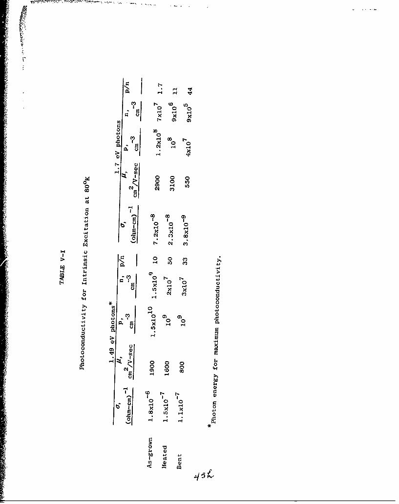
ri r-o 4x4 x
0 3.4.) 0o cr) -~4 OD
X' 0 .
C 9 r0 ' -
H
(n 0
0 0 tf)o C'J Cl)
04. 00O
41 E-I4
Cli 0l 00
E O C 4.)2 -
r-4 o' 0
kk x-
0l 02N I 0
00 a Ho 0'4.4 * 0> 2 41 1 0 0
v40 x -00
0
0 IL0 0
0 0 4-ol (7) IL10
I £4)o0 0 0f 0
00
k IDbb 4-)S 0 .- ~ ~ '-4
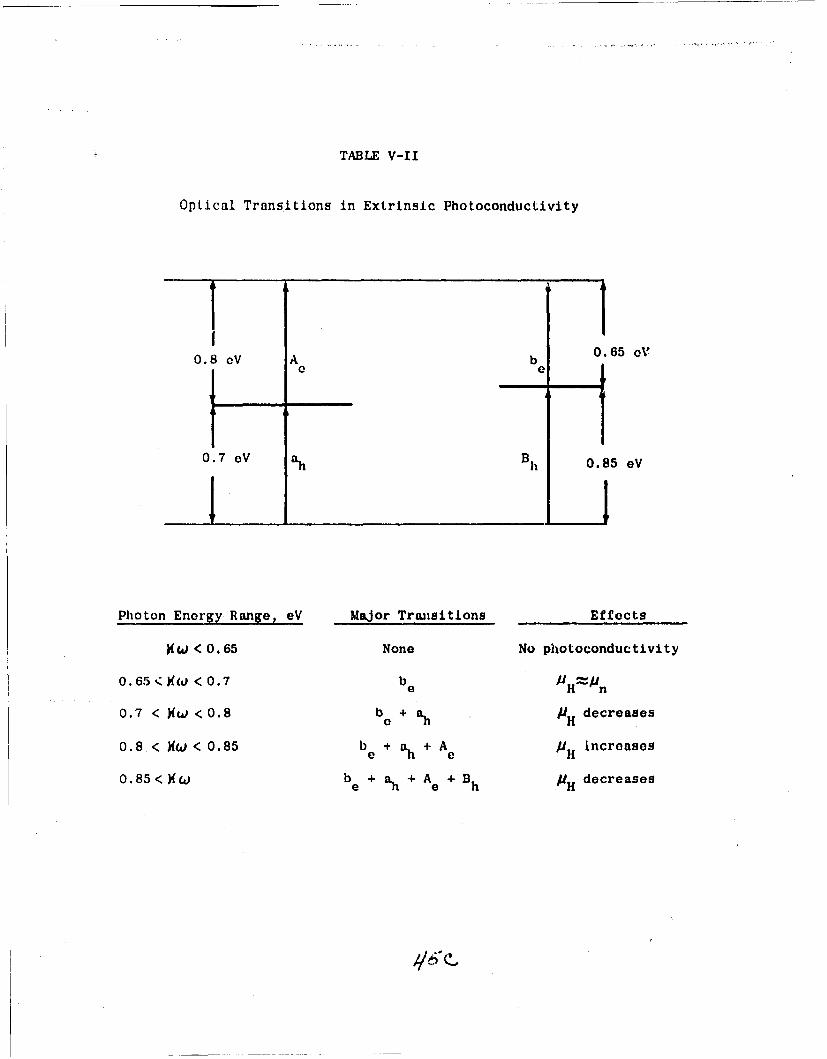
TABLE V-II
Optical Transitions in Extrinsic Photoconductivity
IC0. 8 oV A ° b e 0.65 eV
0.7 oV ah Bh 0.85 eV
Photon Energy Range, eV Major Transitions Effects
w < (0.65 None No phiotoconductivity
0.65 < )(( < 0.7 be MH Mn
0.7 < )tiw < 0.8 b + decreases
0.8 < )W < 0.85 be + ah + Ae #H increases
0.85< )(( be + ah + Ae + Bh PH decreases
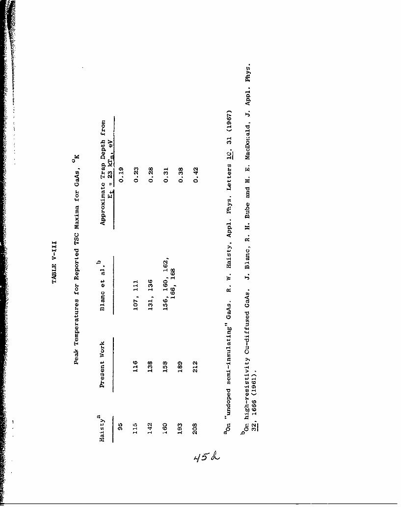
4-z
00
CO)
(4.4
&4 C4
0 E w
0a 00 0+EV
04IV 1m0 U)m r- 00'0 C5.. .0.
0 C)
a). CO 0
-- 4402
-4.4 Cl) tfl 00 r015.D -4 -44 >
0 0 (
0l 4J (D ( V
044 (0I MO COICeP4
Figure Captions
Figure V-i. Temperature dependence of the carrier concentration in n-type GaAs as measured in a helium dewar. Comparison withprevious measurements shows a large discrepancy.
Figure V-2. Temperature dependence of the carrier mobility in n-typeGaAs as measured in a helium dewar. Comparison with pre-vious measurements shows a large discrepancy.
Figure V-3. Spectral response of photoconductivity in the extrinsicrange for GaAs:Cr as-grown, after heating for 1 hour at580%C, and after deformation at 580*C. Measurement atW80K.
Figure V-4, Variation of photo-Hall mobility with exciting photon energyfor GaAs:Cr as-grown, after heating for 1 hour at 580*C, andafter deformation at 580*C. Measurements at 800 K.
Figure V-5. Results of a two-carrier analysis of the data given inFigures V-3 and V-4 using tI mobility values given inthe text.
Figure V-6. Optical quenching of photoconductivity spectra at 80 0 K forGaAs:Cr (1) as-grown, (2) after heating for 1 hour at 580*C,and (3) after deformation at 580*C.
Figure V-7. Thermally stimulated current curves for GaAs:Cr as-grown,after heating for 1 hour at 580*C, and after deformation at580*C. Solid curves are for extrinsic (0.85 eV) photoex-citation, and dashed curves are for intrinsic (1.46 eV) ex-citation.
Figure V-8. Thermally stimulated current curves for deformed GaAs:Crafter the following photoexcitations: (1) white light,f = 1.0; (2) white light, f = O.'; (3) white light, f =0.013; (4) 0.85 eV radiation for 30 min. followed by 1.08-eVquenching radiation for 5 min.
*
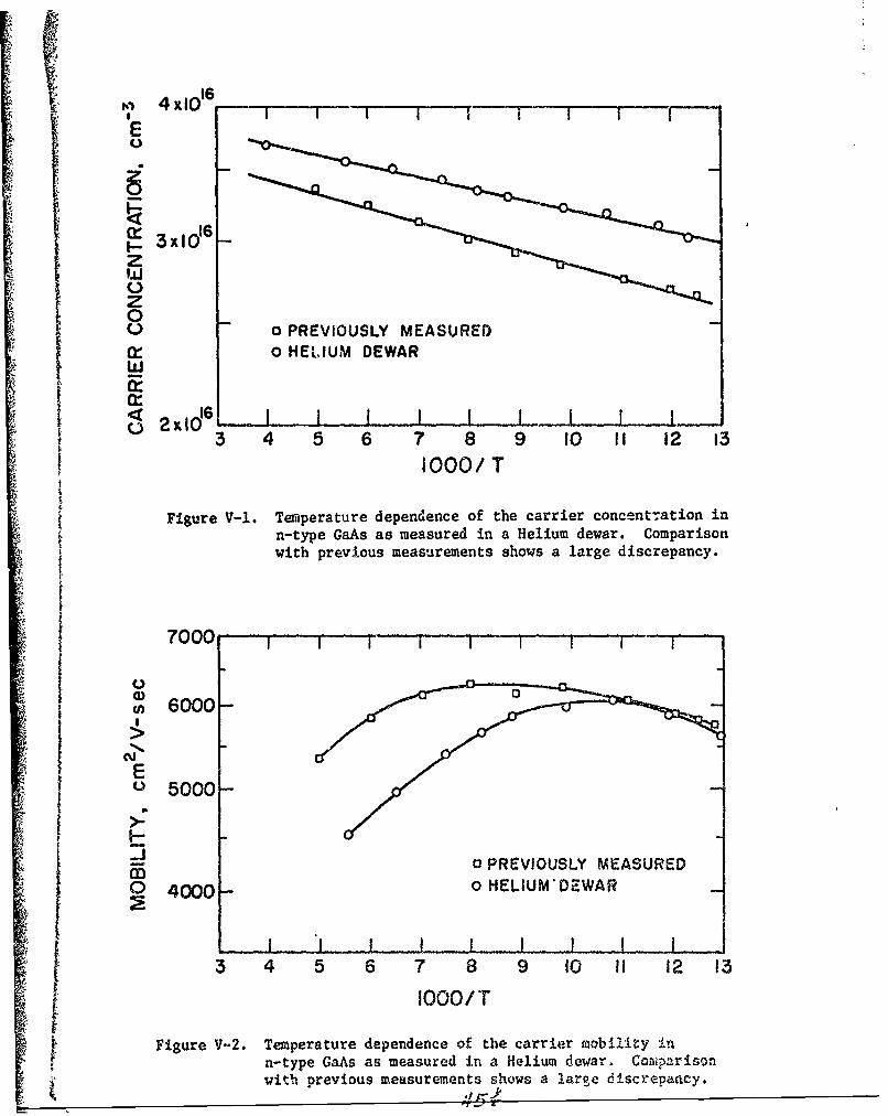
16
r-i 4 x10l ------- ---------I
I. 3xozW0z00 o PREVIOUSLY MEASUREDi 0 HELIUM DEWAR
12io 6 I i .. I I I ! !3 4 5 6 7 8 9 10 !1 12 13
1000/ T
Figure V-1. Temperature dependence of the carrier concentration inn-type GaAs as measured in a Helium dewar. Comparisonwith previous measurements shows a large discrepancy.
7000 .
, 6000
I
5000
j--3 PREVIOUSLY MEASUREDo 4000 0 HELIUM'DEWAR
I L.. ' L ! - J _-I I . I I....L _ _
3 4 5 6 7 8 9 10 II 12 13
1000/T
Figure V-2. Temperature dependence of the carrier mobility itn-type GaAs as measured in a Helium dewar. Comparisonwith previous measurements shows a large discrepancy.
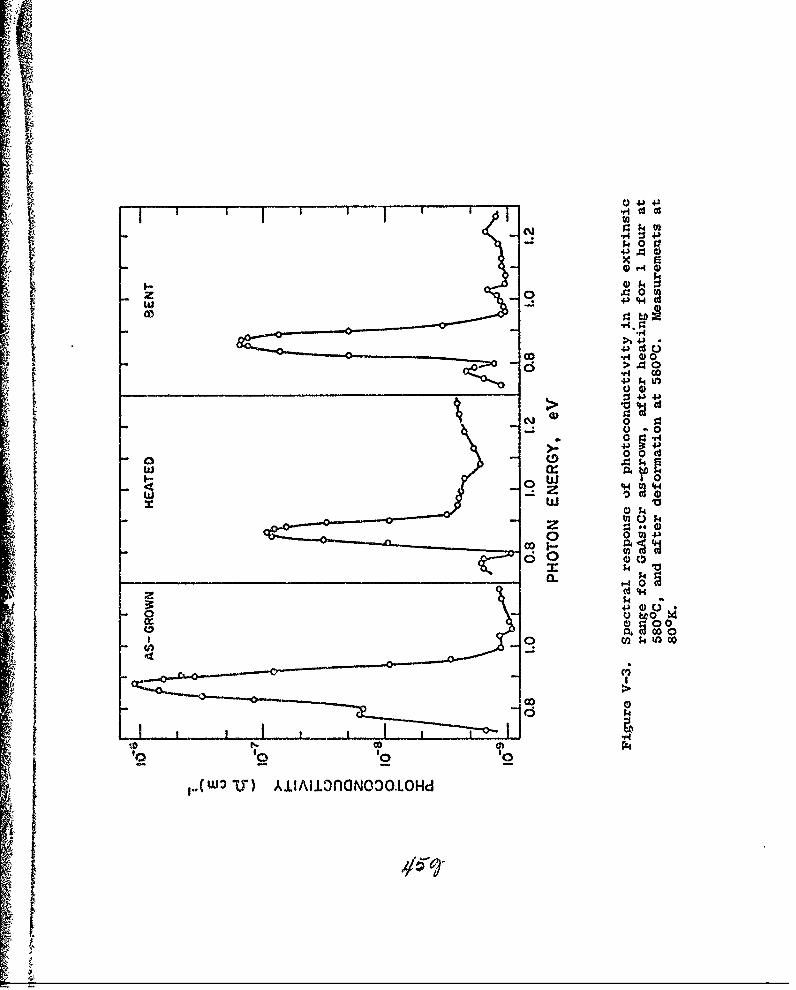
dd r-r :1 4-)T 1
),4 0x 4
S0 c 0zzo
N
9- 0
Z 0 4q 94N *•0 00
r.(W: "U' ,•.IAI.OI'4]NO .LO~
-: 00
ww 4
z C~t4
00
10
'0 W
IT)~~~~ 900J.OlNOOL~
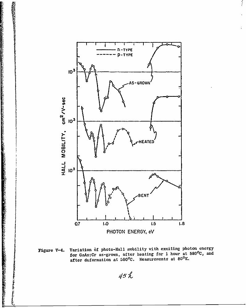
p-TYPE------------------ -- ----------P-TYPE
SAS-GROWN
E 10U
%
< 103
BEN
S0%
V 61I
0t
0.7 hO0 1.5 1.8
Figure V-4. Variation 6f photo-Hall mobility wihectnpoonnryfor GaAs:Cr as-grown, after heating for 1 hour at 5800C, andafter deformation at 5800C. Mleasurements at 80°K.
215
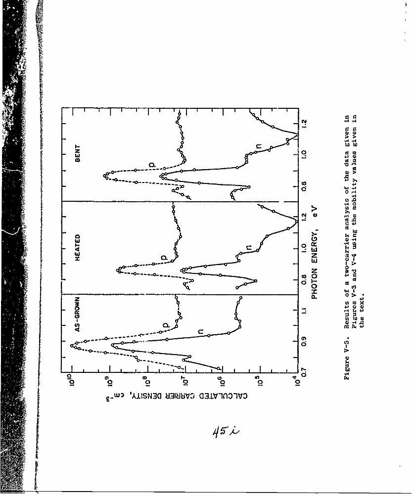
I.' .-'4 *14
z boIAJd - ai
0)
0
Or414
-%%
r4 14 4-
4 '4
00
'AIIN30U31aVO 31V-nxz
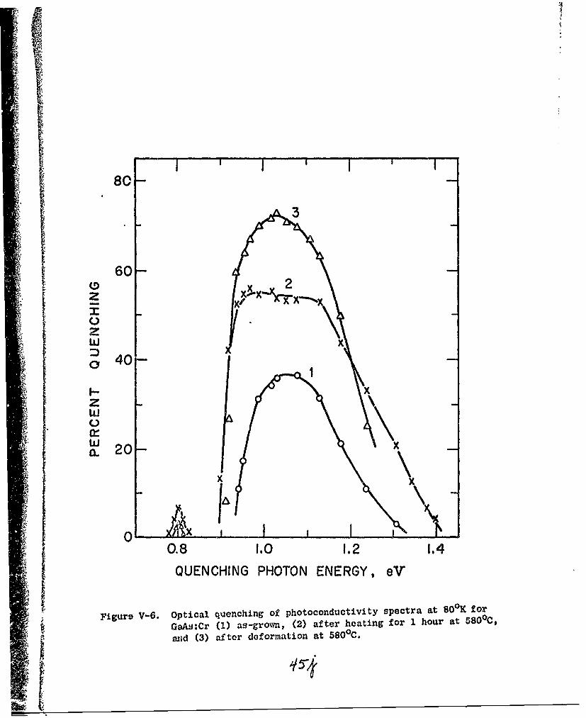
80-
60-2
zK x ..XK..) KWx---
zw K
o 40-
zw0
w xa. 20-
x I! ~-\
0 Lx ... .II, I
0.8 1.0 1.2 1.4
QUENCHING PHOTON ENERGY, eV
Figure V-6. Optical quenching of photoconductivity spectra at 800 K for
GaAs:Cr (1) as-grown, (2) after heating for 1 hour at 580 0 C,
and (3) after deformation at 5800 C.
$1
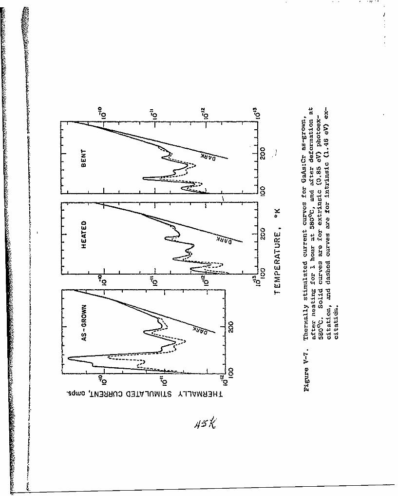
o 0 to 10 to
0 0)
000
0 cc
k 4A
W9 0 0C
44
w N)4
10100 V ,-
"q ý4-) .4~ 'L
4J 0
i~~~ (4 . l
.4 00 04 Cd0 Q 0
E- -0 0b-
*sdw~o 'IN3~ufl3 aawiVnfVUs AT1VVN83Hi d
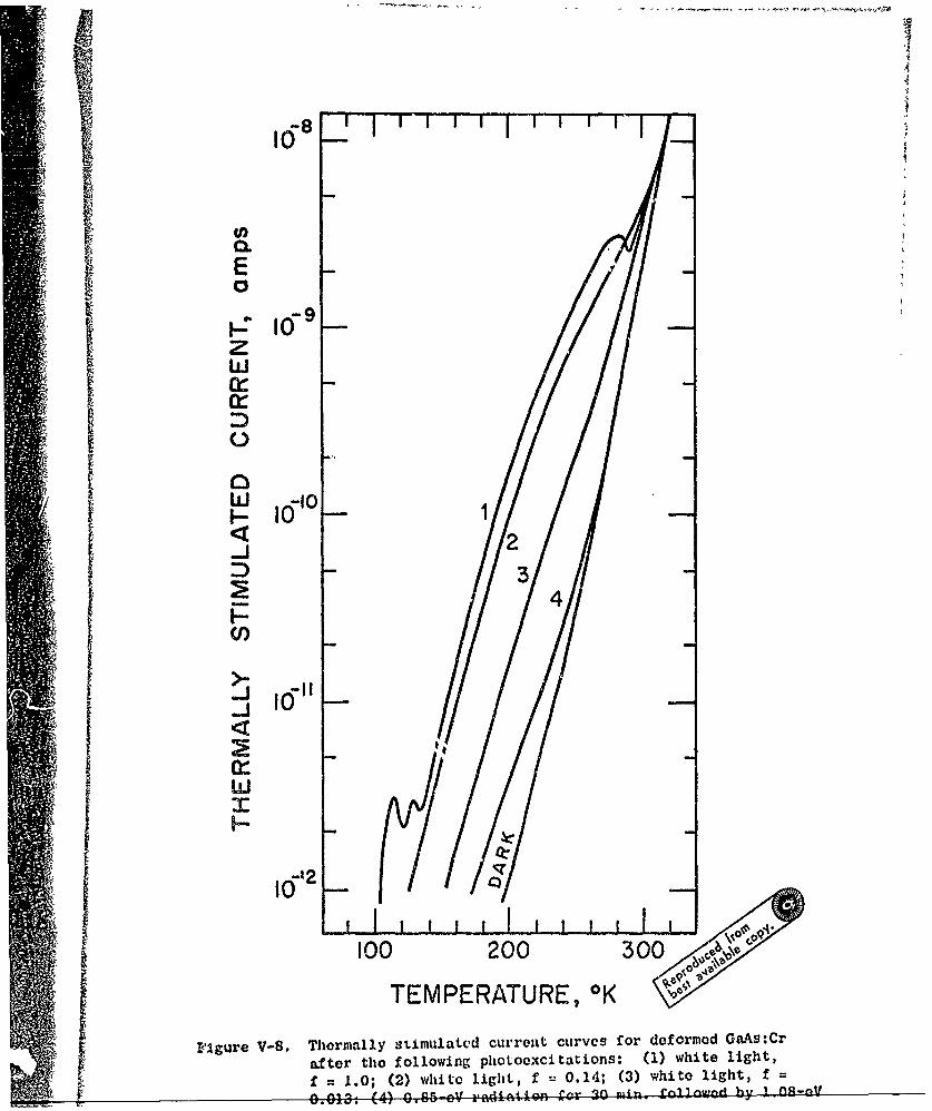
1I8
E
-C9zW
-Ix
I-
C')
hAJ
T
I<
V-2
SI0-
I00 200 300
TEMPERATURE, OK
Figure V-8. Thermally stimulated current curves for deformed GaAs:Cr
after the following photoexcitations: (1) white light,
£ = 1.0; (2) white light, f = 0.14; (3) white light, £ =
VI. SCIENTIFIC ASPECTS OF SEMICONDUCTOR CRYSTAL PREPARATIONW. A. Tiller, B. Jindal and Hyo-Sup Kim.
A. PROGRAM CBJECTIVE
The objective of this investigation is to develop an understanding
of the important interfacial parameters that govern the growth of GaAs
crystals. The study includes the structure and energetics of the GaAs
solid/Ga-As liquid interface as a function of (i) the composition of the
liquid phase and (ii) the orientation of the solid GaAs. In addition,
the concentration distribution in the vicinity of the interface is to be
calculated.
B. PROGRESS
In the previous studies, a semi-microscopic method was developed to
determine the structure and energetics of the solid-liquid solution in-
terfaces for the III-V compounds, and sample calculations were made for
the Ga-As system by using simple parametric interatomic interaction
functions. The most recent progress falls into three categories:
1. Average Atomic Interaction Energy for Ga-As Liquid Solution
Stressing the importance of accurate knowledge concerning the inter-
atomic interaction energies in our study, we have sought to construct
more suitable interaction energy functions for the liquid solution than
for those developed previously. Without splitting the energy function
into individualized components, average atomic interaction energy func-
tions have been determined in the Morse potential function form at given
concentrations by using the available data on atomization energies,
average atomic positions, and compressibilities. The parameters for the
'4P
functions were found to exhibit a satisfying self-consistency and axe
tabulated in Table VI-I.
2. Distribution of the Interaction Energies in the Interface Region
More details on the quasi-chemical contributions have been studied
using a similar method to that introduced in previous reports. The
xsolid-liquid interaction energies, LESL, and Lhe excess energies, AE
associated with the formation of the planar interface at each layer on
the liquid side of the interface region, have been calculated for dif-
ferent concentrations along the liqvtdus line and for different orienta-
tions o:Z the crystal. The energy distributions for (L11A and B)/liquid
solution are tabulated in Table VI-II.
3. Relaxation of the First Layer Spacing at the Interface.
Minimizing the total interaction energies, one can determine the
relaxed (equilibrium) spacing of the atomic layers Ft the interface re-
gion. The first layer spacings, di, and the variation of the interaction
energies, AE X, due to the relaxation have been calculated and tabulated
in Table VI-III.
C. FUTURE WORK
Using the composition and orientation dependence of iiterface ad-
sorption, the situation at layer edges will be evaluated tj determine
both interfacial energy and interface attachment kinetics as a function
of orientation and liquid composition. From the edge energy aspects,
one can evaluate the ease or difficulty of creating layer edges at cer-
tain orientations. From the density of edge Rinks and adsorbed Ga atoms,
one can evaluate the driving forces needed for mation of the layer edges
47
along faces of differen, orientations a'Ad along different directions in
those faces.
In addition, using a recent theoretical advance relating to the cre-
ation of interface.ý during phase transformations, the stability of dif-
ferent faceted interfaces in the GaAs system will be evaluated and a
qu-titative condition governing their breakdown developed. Using an
experimental procedure involving Ihe growth of bulk GaAs from solutan
at different Lemperatures and different supersaturations, this instabil-
ity condition will be experimentally tested. The results of this ex-
perimentLI theoretical correlation should be directly applicable to the
" {• epitaxiat growth of GaAs layers.
Sr
AVC•0
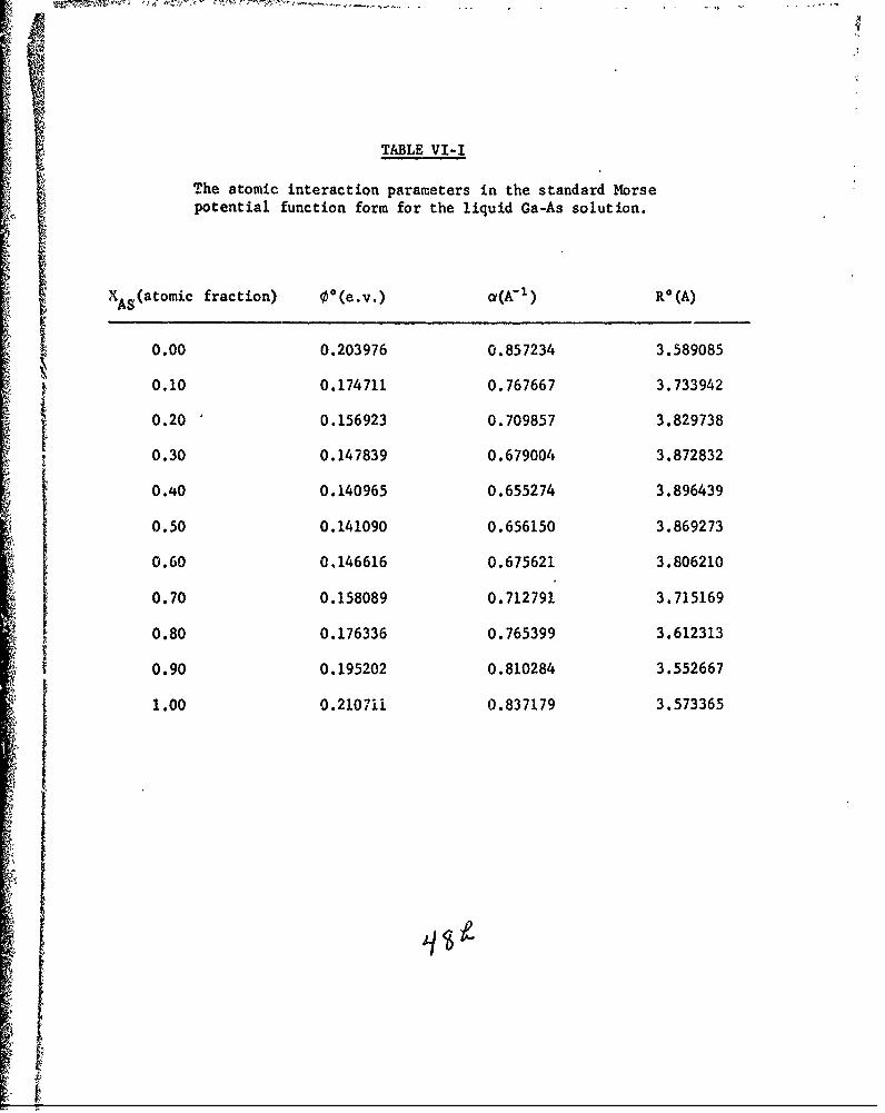
TABLE VI-I
The atomic interaction parameters in the standard Morsepotential function form for the liquid Ga-As solution.
XAS(atomic fraction) 0*(e.v.) ci(A-) R0 (A)
0.00 0.203976 0.857234 3.589085
0.10 0.174711 0.767667 3.733942
0.20 0.156923 0.709857 3.829738
0.30 0.147839 0.679004 3.872832
0.40 0.140965 0.655274 3.896439
0.50 0.141090 0.656150 3.869273
0.60 0.146616 0.675621 3.806210
I0.70 0.158089 0.712791 3.715169
0.80 0.176336 0.765399 3.612313
0.90 0.195202 0.810284 3.552667
1.00 0.2107ii 0.837179 3.573365
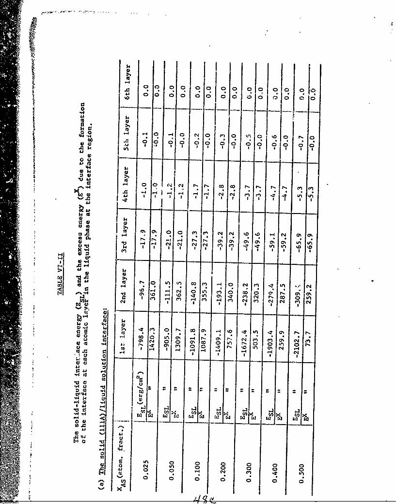
00000 01~0 0 0
0 c. o C;Jo^
0 -40,H _P4-4 0 HO NO C 0 vo tna NO 0 !0
74 ~ 0 00 00 0 0 0 00 0
4.4
-A I.u"4
P44 J~ N N~ 04 cn cn Ln r. t vn
> 41
P4 040n.C CE4 ,. 0 %O% 00 ol' Np N- ON~ H %0
004
w. Cf% " -. a N. 4% 00 0 % 0% 0% 0% 0% U,%V HH N- NT NA Nn Cl Cl %D Uttu4 S S S I I I SU Cl
r4 0 .
U. -- 0jo ~ U H d - , *'* 9 A 9 A * 9 A * * to
P-4 0 1 l 0 ~ 0 0 . O 0
i ~ ~ ~ ~ c ch En~C ~ ' ~ ' v
9 (A *
o 0
41 4
0 H
XI k H 0 0 0
Li 0 0 "4 N clE~l f A *A A
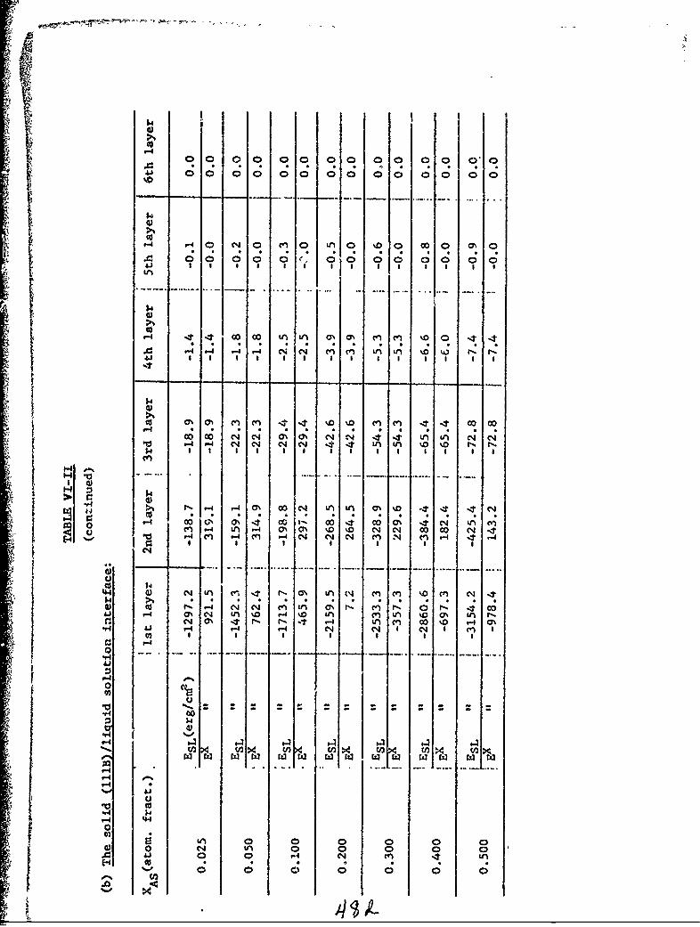
14
r4
00 000 0 0 0 00o
.41
0n in OO t0% MO 0n -00 It 0
00 0 0% OO. 0nc0 00 00 c 00
5.4
0ý co 04¶ a n 01 (7% %0 C 0 4
u ~ 10 4 M -4 M4 "4 4 N N Cl Cl Mfu 11 N
E4.
m 00 N N4 011C;4 lL'-4 0% -4 LN ND N 0 N n %D C% LA . 0 N N
I 0
H 0
4) C .4 L - 011 0 0 N Nn 00 N 4~4C v4C; 04 C; C; C44-
0 41
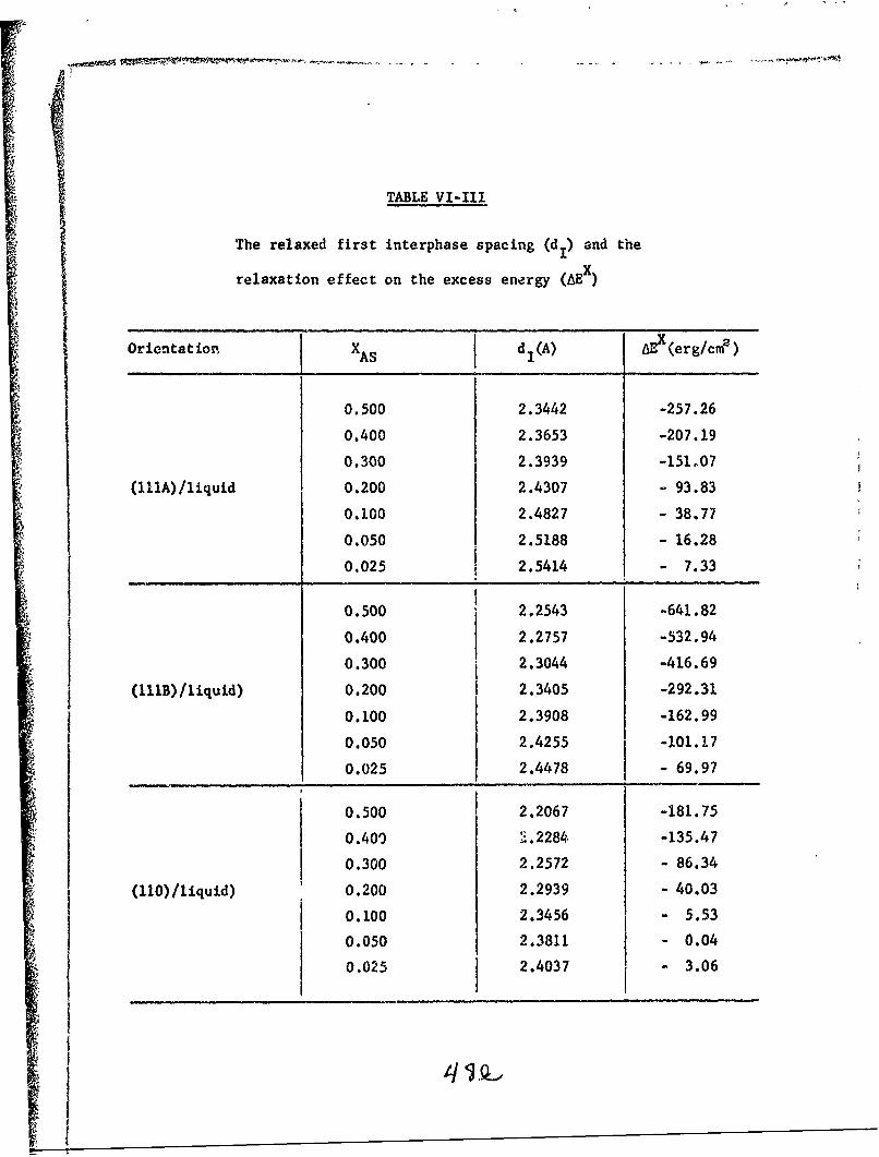
TABLE VI-III
The relaxed first interphase spacing (di) and the
relaxation effect on the excess energy (AE )
Orientation XAS dI(A) E(erg/cm2)
0.500 2.3442 -257.26
0.400 2.3653 -207.19
0,300 2.3939 -151.07
(lIlA)/liquid 0.200 2.4307 - 93.83
0.100 2.4827 - 38.77
0.050 2.5188 - 16.28
0.025 2.5414 - 7.33
0.500 2.2543 -641.82
0.400 2.2757 -532.94
0.300 2.3044 -416.69
(l1lB)/liquid) 0.200 2.3405 -292.31
0.100 2.3908 -162.99
0.050 2.4255 -101.17
0.025 2.4478 - 69.97
0.500 2.2067 -181.75
0.409 i.2284 -135.47
0.300 2.2572 - 86.34
(110)/liquid) 0.200 2.2939 - 40.03
0.100 2.3456 - 5.53
0.050 2.3811 - 0.04
0.025 2.4037 - 3.06
VII. VAPOR-PHASE GROWTH OF AIN, GaN AND AiN -GaN SOLID SOLUTIONSD. A. Stevenson and H. P. Maruska
A. PROGRAM OBJECTIVES
AIN is a wide bandgap (5.9 eV) semiconductor with an as-grown re-
sistivity of about 1012 ohm-cm. Owing to the lack of a center of sym-
metry in its wurtzite crystal structure, it exhibits piezoelectricity
and, thus, ic of interest as an ultrasonic transducer material. Little
information is available concerning its electrical and optical properties.
GaN has a bandgap of 3.5 eV, and much more interest has developed
recently in this material. Green and blue electroluminescent diodes have
been fabricated in i-n junction layers of GaN. The n-layer is uninten-
tionally doped but always contains more than 10 electrons/cm3 (probably
due to a native defect) while the insulating (i) layer is produced by
compensating with the deep acceptor zinc.
It is of interest to study solid solutions of AIN and GaN. Both
materials are hexagonal (wurtzitc) with similar lattice parameters, and
the radii (either ionic or covalent) of Al and Ga are almost identical.
Therefore, it is reasonable to expect that a continuous series of solid
solutions should form. Hewever, no report of these has ever been made
in the literature. Since the resistivity of "undoped" GaN is 10-3 ohm-
cm, the resistivity should change by 15 orders of magnitude for the
scrios of solid solutions formed between GaN and A1N. If these can be
formed, (he carrier concentration should also drop through the series
by many ordc,• of magnitude, and a useful range of about 10 14-1015 elec-
trons/cma3 may bo A.ouid.
49
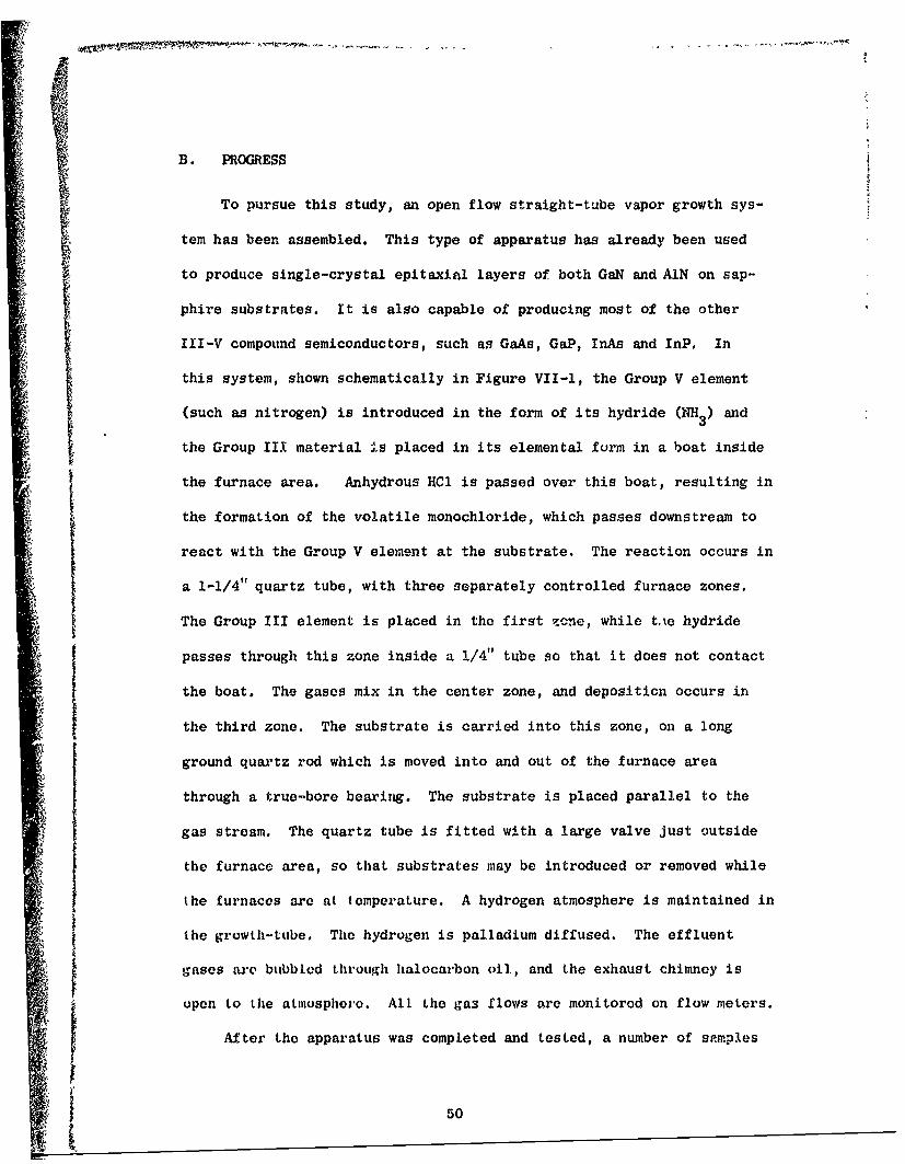
B. PROGRESS
To pursue this study, an open flow straight-tube vapor growth sys-
tem has been assembled. This type of apparatus has already been used
to produce single-crystal epitaxial layers of both GaN and AIN on sap-
phire substrates. It is also capable of producing most of the other
III-V compound semiconductors, such as GaAs, GaP, InAs and InP. In
this system, shown schematically in Figure VII-l, the Group V element
(such as nitrogen) is introduced in the form of its hydride (NH 3 ) and
the Group III material is placed in its elemental form in a boat inside
the furnace area. Anhydrous HCl is passed over this boat, resulting in
the formation of the volatile monochloride, which passes downstream to
react with the Group V element at the substrate. The reaction occurs in
a 1-1/4" quartz tube, with three separately controlled furnace zones.
The Group III element is placed in the first zone, while t.te hydride
passes through this zone inside a 1/4" tube so that it does not contact
the boat. The gases mix in the center zone, and deposition occurs in
the third zone. The substrate is carried into this zone, on a long
ground quartz rod which is moved into and out of the furnace area
through a true-bore bearing. The substrate is placed parallel to the
gas stream. The quartz tube is fitted with a large valve just outside
the furnace area, so that substrates may be introduced or removed while
the furnaces are at temperature. A hydrogen atmosphere is maintained in
the growth-tube. The hydrogen is palladium diffused. The effluent
gases are bubbled through halocarbon oil, and the exhaust chimney is
open to the atmosphere. All the gas flows are monitored on flow meters.
After the apparatus was completed and tested, a number of semples
50
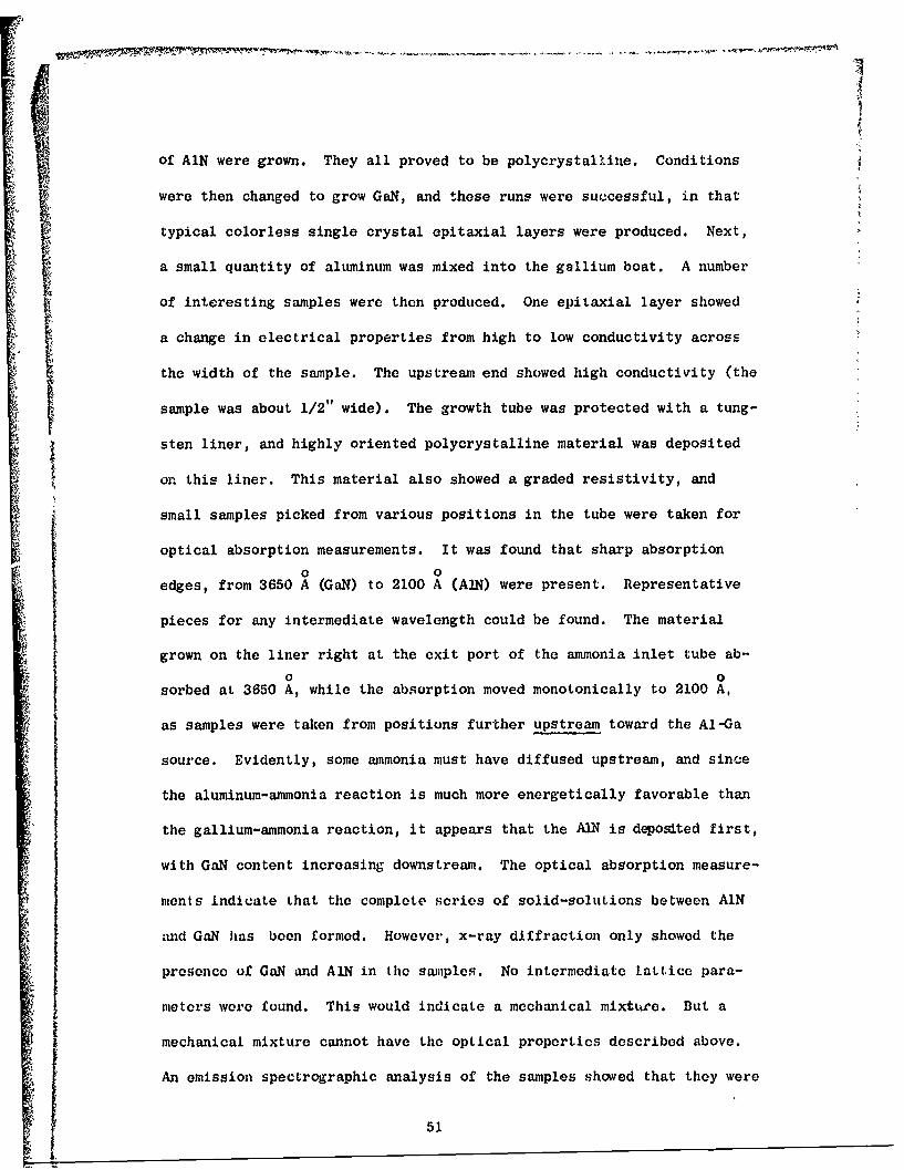
of AIN were grown. They all proved to be polycrystalline. Conditions
were then changed to grow GaN, and these runs were successful, in that
typical colorless single crystal epitaxial layers were produced. Next,
a small quantity of aluminum was mixed into the gallium boat. A number
1 of interesting samples were then produced. One epitaxial layer showed
a change in electrical properties from high to low conductivity across
the width of the sample. The upstream end showed high conductivity (the
sample was about 1/2" wide). The growth tube was protected with a tung-
4 sten liner, and highly oriented polycrystalline material was deposited
on this liner. This material also showed a graded resistivity, and
small samples picked from various positions in the tube were taken for
optical absorption measurements. It was found that sharp absorption
0 0edges, from 3650 A (GaN) to 2100 A (AIN) were present. Representative
pieces for any intermediate wavelength could be found. The material
grown on the liner right at the exit port of the ammonia inlet tube ab-
0 0sorbed at 3650 A, while the absorption moved monotonically to 2100 A,
as samples were taken from positions further upstream toward the Al-Ga
source. Evidently, some ammonia must have diffused upstream, and since
the aluminum-ammonia reaction is much more energetically favorable than
the gallium-ammonia reaction, it appears that the AIN is deposited first,
with GaN content increasing downstream. The optical absorption measure-
ments indicate that the complete series of solid-solutions between AIN
and GaN has been formed. However, x-ray diffraction only showed the
presence of GaN and A1N in the samples. No intermediate lattice para-
meters were found. This would indicate a mechanical mixture. But a
mechanical mixture cannot have the optical properties described above.
An emission spectrographic analysis of the samples showed that they were
51I,. . .
indeed only compounds of aluminum, gallium and nitrogen, so the adsorp-
tion is not being caused by some spurious unknown material. We have ten-
tatively surmised that the samples may be amorphous (with the crystals
grown during the initial pure GaN and AIN runs.)
C. FUTURE PLANS
The apparatus is being modified so that the Al and Ga sources can
be placed in separate tubes with separate controls. Substrates will be
placed between the ammonia inlet tube port and the source boat so that
the grown layers can be easily removed, since the tungsten liner itself
is difficult to remove, and requires dismantling the system.
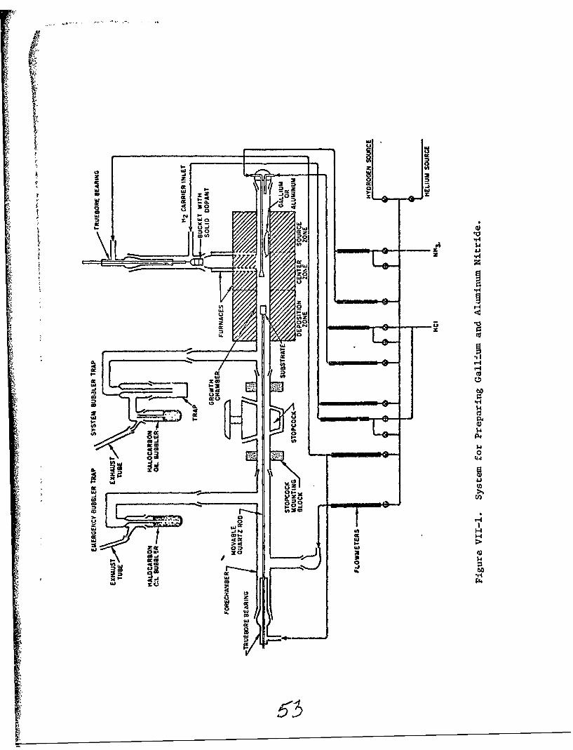
z at
w4 J
cc us
9-~~I .L-J4
IL P4
4 0200s
w 04444
IN0
036 0 -
> -t
00
1*1
a F


![Sensors and Actuators B: Chemicalorca.cf.ac.uk/98123/1/Post print.pdfsensors based on semiconducting oxides, including the synthesis of different morphologies [4], doping [5], surface](https://img.pdfslide.net/doc/110x75/6108252b4c61d439e975242d/sensors-and-actuators-b-printpdf-sensors-based-on-semiconducting-oxides-including.jpg)