Embed Size (px)
Citation preview

Network for Computational Nanotechnology (NCN) UC Berkeley, Univ.of Illinois, Norfolk State, Northwestern, Purdue, UTEP
First-Time User Guide to OMEN Nanowire**
Sung Geun Kim*, Saumitra R. Mehrotra, Ben Haley, Mathieu Luisier, Gerhard Klimeck
Network for Computational Nanotechnology (NCN) Electrical and Computer Engineering
*[email protected] ** https://nanohub.org/resources/5359

Sung Geun Kim
• Introduction 3 → What is a nanowire? → What is a nanowire FET? → What can be measured in a nanowire FET? → What is Omen?
• What Can Be Simulated by the OMEN Nanowire?: input 8
• What if You Just hit “Simulate”?: output 13
• Examples of Simulation Runs (input-output relationship) 15 → What if the length of the channel is changed? → What if the diameter of the nanowire is changed?
• Limitations of the OMEN Nanowire Tool 19
• On-Demand Simulation: A Few Points to Consider 20
• References 21
Table of Contents

Sung Geun Kim
Introduction: What is a Nanowire?
nanowire: wire-like structure with diameter or lateral dimension of nanometer(10-9m)
~10-9m=1nm
http://en.wikipedia.org/wiki/DNA
~Size of DNA
→ Various material systems can be used to fabricate nanowires. For example: silver, gold, copper, …, etc. (metal) Si, Ge, GaAs, GaN, …, etc. (semiconductor)
3

Sung Geun Kim
What is a Nanowire?
Fig 2. http://www.spectrum.ieee.org/oct07/5642
Fig. 3 Nanowire FET
Fig. 1 **Nanowire memory cell
Fig 1. http://www.eurekalert.org/pub_releases/2004-04/uosc-spn042004.php
Fig. 2 ***Nanowire LED Fig 3. http://www.nist.gov/public_affairs/techbeat/tb2005_0630.htm#transistors
National Institute of Standards and Technology
B. Tian, Lieber Group, Harvard University
Application of nanowires
4

Sung Geun Kim
What is a Nanowire FET?
nanowire FET: field effect transistor(FET) using nanowire
Gate
Channel Insulator Source
Drain
Current
» The current from the source to the drain is turned on and off by the voltage applied to the gate.
» Because the gate in nanowires is surrounding the channel, it can control the electrostatics of the channel more efficiently than the conventional MOSFET.
On Off
5

Sung Geun Kim
What Can Be Measured in a Nanowire FET?
IV Characteristics[1](Id-Vg, Id-Vd)
(a) Id-Vg (b) Id-Vd
[1] Sung Dae Suk, et. al., IEDM, 2005, “High Performance 5nm radius Twin Silicon Nanowire MOSFET(TSNWFET) : Fabrication on Bulk Si Wafer, Characteristics, and Reliability
Vg Vd
Id
Vg Vd
Id
6

Sung Geun Kim
What is OMEN?
OMEN[3,4] : atomistic full-band quantum transport simulator
Source Drain
Gate
Carrier transport
[3] Mahieu Luisier, et. al., Physical Review B, 2006 [4] http://cobweb.ecn.purdue.edu/~gekco/omen/index.html
Atomistic description of bandstructure – sp3d5s* tight binding model +3D Poisson and Schrodinger equation [3,4]
Wave Function Approach[3,4]
7

Sung Geun Kim
What Can Be Simulated by OMEN Nanowire?
OMEN Nanowire can simulate nanowire FETs of different types. You can choose between a rectangular nanowire and a circular nanowire.
Gate
Channel
Rectangular Nanowire
Insulator
Circular Nanowire
Channel Insulator
8
Device Type

Sung Geun Kim
What Can Be Simulated by OMEN Nanowire?
Nanowire FETs of various sizes
Geometry-X Geometry-Y Geometry-Z
9
Device Structure - Geometry
Sung Geun Kim
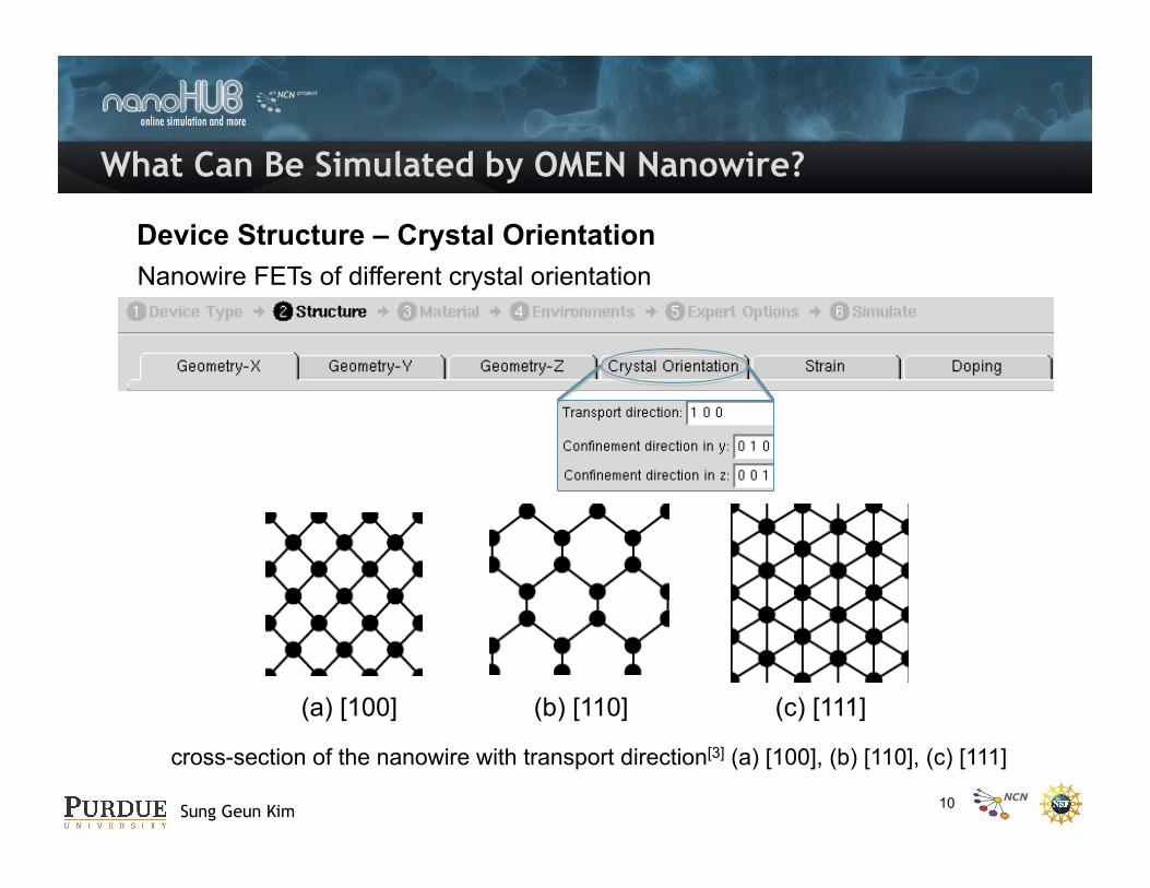
What Can Be Simulated by OMEN Nanowire?
Nanowire FETs of different crystal orientation
(a) [100] (b) [110] (c) [111]
cross-section of the nanowire with transport direction[3] (a) [100], (b) [110], (c) [111]
10
Device Structure – Crystal Orientation
Sung Geun Kim
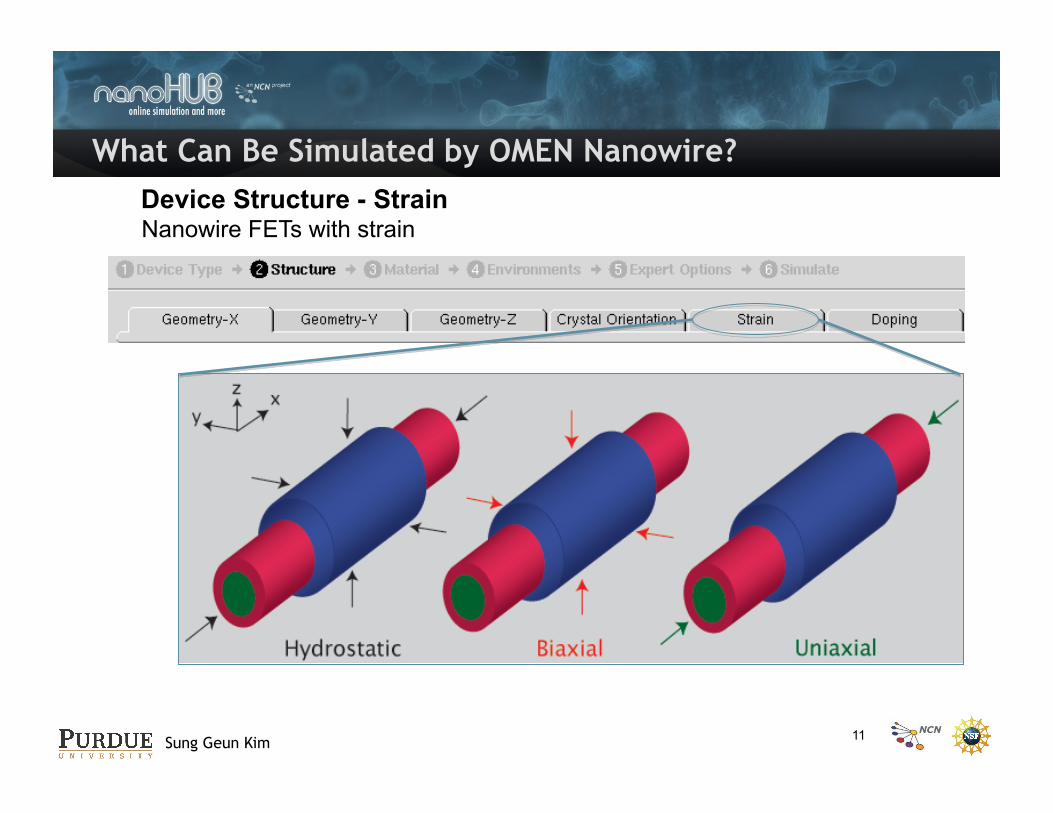
What Can Be Simulated by OMEN Nanowire?
Nanowire FETs with strain
11
Device Structure - Strain

Sung Geun Kim
What Can Be Simulated by OMEN Nanowire?
OMEN Nanowire can simulate nanowire FETs of different material and environment parameters.
12
Material/Environment

Sung Geun Kim
What If You Just Hit “Simulate”?
You will get the result immediately with the following message!
• To submit a new simulation, change other input parameters such as the structure, material, environment parameters. The estimated walltime/memory usage[5] to run the simulation will post after “Simulate” is clicked.
[5]http://cobweb.ecn.purdue.edu/~gekco/students/SungGeunKim/SungGeunKim_OMENNanowire_time_table.html
13

Sung Geun Kim
Outputs
Sequence plot
Click!
• [Inputdeck] : Input parameters translated to the format that can be used for job submission to OMEN
• [Id-Vg Characteristics] : Id-Vg curve (Id-Vd curve can be chosen to be shown in the environment input option)
• [1D electron density] : 1D electron density (/cm3) to the transport direction
• [1D bandstructure] : 1D bandstructure/Fermi levels in the contacts/transmission coefficient/current density/conduction band edge through the nanowire
• [Density of states (x,E)] : 2D density of states as function of transport direction x and energy E
• [Transmission and current density] : Transmission coefficient and the current density(=Transmission*(fL-fR) fL/fR:fermi function at the left and right contact)
• [3D electron density] • [3D electron density(log)] : log scale of 3D electron
density • [3D electrostatic potential] • [Output Log] : includes all the messages posted on the
screen after you click “Simulate” and the output/error messages from the OMEN simulator
14

Sung Geun Kim
Example: What if the length of the channel is changed?
DecreasingLc
Lc:ChannelLength=GateLength
Duetotunnelingcurrent*
The drain current and subthreshold swing** at small Vg increases due to the tunneling current and as the channel length decreases.
* Id(A/µm) - drain current is normalized by the circumference of the nanowire ** subthreshold swing is defined as the inverse of the slope of log10 Id vs Vg curve = ∂(log10 Id)/ ∂ Vg
SubthresholdSwing**increasing
15
IV Characteristics

Sung Geun Kim
Example: What Happens at a Small Channel Length? (bandstructure)
Current Density*
Transmission
Bandstructure at the Right Contact
Bandstructure at the Left Contact
Conduction Band Edge
Tunneling
Channel length = 4nm
Vg=0V, Vd=0.4V
Source Drain
*Current Density =Transmission*(fL-fR)
fL:left contact fermi function fR:right contact fermi function
16

Sung Geun Kim
Example: What if the Nanowire Diameter is Changed? (IV Characteristics)
IncreasingDch
Vth*decrease
* Vth can be defined in many ways. Here we define it as a voltage where the drain current becomes larger than certain value (10-7A/µm)
Dch:diameterofcircularnanowire
17

Sung Geun Kim
Example: What happens in the channel?
IncreasingDch
Source
Drain
Channel
Electron density in the channel increases as the diameter of the nanowire increases. → Drain current increases at large diameter nanowire
Drain
Id(A/µm)
Vg(V)
Vg=0V, Vd=0.4V
18

Sung Geun Kim
• Cross section of nanowire cannot be larger than 3X3 nm2 or smaller than 1.5X1.5nm2
• Length of gate should be less than 60 nm
• You can not choose which server or the number of CPUs* in that server to use
• Simulation may not be converged at high Vg (e.g. larger than 0.7V) when the potential barrier is about the same as the conduction band edge of the source side[6]
Limitations of the OMEN Nanowire Tool
*The number of CPUs is estimated by the OMEN Nanowire according to the time table[5] database and as based on the cross section and gate length of the nanowire that user inputs.
[6] https://nanohub.org/resources/6315 19

Sung Geun Kim
On-demand Simulation
• The number of CPUs for which OMEN Nanowire can submit a job, in order to end the simulation in 4 hours* in a steele cluster, is less than 256.
• If your simulation needs more than 256 CPUs, the simulation will be aborted and the following message will appear:
• If you want to simulate structure that uses more than 256 CPUs, or if you want to simulate with a different material system than what is now provided in OMEN Nanowire, you may submit a request for a device that can manage such a job. Contact the developer team by email ([email protected]) or by webpage
(https://nanohub.org/resources/5359/questions).
*This is the walltime limit in steele cluster
20

Sung Geun Kim
• Experimental Study on Nanowire FET [1] Sung Dae Suk, et. al., IEDM, 2005, “High Performance 5nm radius Twin Silicon Nanowire
MOSFET(TSNWFET) : Fabrication on Bulk Si Wafer, Characteristics, and Reliability • Physics of Nanowire FET [2] Wang, Jing (2006), "Device Physics and Simulation of Silicon Nanowire Transistors,"
http://nanohub.org/resources/1313 • OMEN [3] Mahieu Luisier, et. al., “Atomistic simulation of nanowires in the sp3d5s* tight-binding
formalism : From boundary conditions to strain calculations”, Physical Review B,2006 [4] http://cobweb.ecn.purdue.edu/~gekco/omen/index.html • Time/memory estimation in OMEN Nanowire [5]
http://cobweb.ecn.purdue.edu/~gekco/students/SungGeunKim/SungGeunKim_OMENNanowire_time_table.html
• The Limitation of the OMEN Nanowire at high gate voltage [6] OMEN Nanoiwre Supporting Document : Limitation of the Tool at Large Gate Voltage - https://nanohub.org/resources/6315
21
References