Embed Size (px)
Citation preview
REVIEW
1802211 (1 of 20) © 2018 WILEY-VCH Verlag GmbH & Co. KGaA, Weinheim
www.advmat.de
Folding 2D Structures into 3D Configurations at the Micro/Nanoscale: Principles, Techniques, and Applications
Zhe Liu, Ajuan Cui, Junjie Li,* and Changzhi Gu*
Dr. Z. Liu, Dr. A. Cui, Prof. J. Li, Prof. C. GuBeijing National Laboratory for Condensed Matter PhysicsCollaborative Innovation Center of Quantum MatterInstitute of PhysicsChinese Academy of SciencesBeijing 100190, ChinaE-mail: [email protected]; [email protected]
The ORCID identification number(s) for the author(s) of this article can be found under https://doi.org/10.1002/adma.201802211.
DOI: 10.1002/adma.201802211
configurations are no longer sufficient, either in terms of realizing certain cru-cial functionalities or in performance improvement. Compared to 2D structures, 3D structures have one more dimension, which enables more diversity in structure/device design and is crucial in realizing richer physical interactions, better per-formance, and advanced functionalities. For example, to obtain a negative perme-ability from split ring resonators (SRRs) to construct negative index metamaterial, a vertical configuration of SRRs is needed to couple with the magnetic field, while planar SRRs can only couple with the elec-tric field to obtain a negative permittivity.[4] With respect to device performance, 3D gold helixes[5] have larger polarization contrast than 2D chiral structures,[6] and dynamic 3D microcontainers[7] can realize drug delivery in a much more controllable way than absorption on 2D structures.[8] Therefore, 3D micro/nanostructures are of significant importance in such scenarios, acting as an indispensable
supplement to the present 2D micro/nanostructures. However, the fabrication of 3D micro/nanostructures is a formidable challenge with the state-of-the-art equipment, because the tra-ditional planar process cannot be used directly due to its 2D projection nature.
Much effort has been devoted in past decades, and signifi-cant progress has been demonstrated with 3D micro/nanofab-rication, which can be divided into two types of strategies. The first one is brand new technologies/equipment development, including 3D laser direct writing (LDW)[9] and focused ion beam (FIB)[10] processing using two-photon polymerization and ion beam milling/deposition to construct 3D structures. Great scientific advantages have been demonstrated in the fields of mechanics, optics, and biology using these techniques.[11] How-ever, due to their intrinsic point-by-point writing style, the effi-ciency of LDW and FIB is limited. Moreover, the materials that can be proceeded by the two techniques are usually photoresists (two-photon absorption) and metals (FIB-assisted deposition), and transferring to other materials can be quite challenging in most cases.[5,12] The other strategy is a combination or modi-fication of the technologies in planar processes (including lithography, deposition, and etching) and is referred to as “planar technology” in this review. In this strategy, a variety of 3D fabrication methods have been developed, such as multi-layer stacking,[13] oblique angle deposition,[14] and self-aligned
Compared to their 2D counterparts, 3D micro/nanostructures show larger degrees of freedom and richer functionalities; thus, they have attracted increasing attention in the past decades. Moreover, extensive applications of 3D micro/nanostructures are demonstrated in the fields of mechanics, biomedicine, optics, etc., with great advantages. However, the mainstream micro/nanofabrication technologies are planar ones; therefore, they cannot be used directly for the construction of 3D micro/nanostructures, making 3D fabrication at the micro/nanoscale a great challenge. A promising strategy to overcome this is to combine the state-of-the-art planar fabrication tech-niques with the folding method to produce 3D structures. In this strategy, 2D components can be easily produced by traditional planar techniques, and then, 3D structures are constructed by folding each 2D component to specific orientations. In this way, not only will the advantages of existing planar tech-niques, such as high precision, programmable patterning, and mass produc-tion, be preserved, but the fabrication capability will also be greatly expanded without complex and expensive equipment modification/development. The goal here is to highlight the recent progress of the folding method from the perspective of principles, techniques, and applications, as well as to discuss the existing challenges and future prospectives.
3D Micro/Nano Structures
1. Introduction
With the development of micro/nanofabrication technolo-gies, microelectronic devices such as transistors, sensors, and photodetectors have been largely reduced in size, which influ-ences our daily life in extensive ways. For example, laptops, cell phones, and digital cameras are now much more port-able with more advanced functionalities integrated. Remark-able progress has also been made in other fields, such as micro/nano-electromechanical systems (MEMS/NEMS),[1] photonics,[2] and biomedicine,[3] in realizing high-performance device miniaturization, and high-density integration. Most of the abovementioned advancements are made with 2D micro/nanostructures/devices, yet in many scenarios, the 2D
Adv. Mater. 2019, 31, 1802211
© 2018 WILEY-VCH Verlag GmbH & Co. KGaA, Weinheim1802211 (2 of 20)
www.advmat.dewww.advancedsciencenews.com
membrane projection lithography.[15] Each method has demon-strated its unique advantage in 3D fabrication, and various 3D patterns with unprecedented structure complexity and fabrica-tion precision have been fabricated. However, some challenges remain; for example, multilayer alignment with nanoscale precision is not only time consuming but also requires an expensive alignment system, and, for oblique angle deposi-tion and self-aligned membrane projection lithography, the structure of the fabricated patterns is restricted to the sup-porting frame and mask shape, etc. One of the most common challenges is the fabrication of 3D patterns with flexible ori-entations from various materials. In this regard, the folding technique, by which 3D structures can be constructed through the folding of 2D films, has begun to draw increasing attention. By controlling the size/shape of each 2D element and especially the relative orientation between them, various 3D structures can be fabricated with unprecedented structure complexity. Moreover, 3D structures from a broad range of materials, including metals, ceramics, polymers, and composites, can be obtained with this method. Due to the 2D nature of the folding technique, the advantages of the traditional planar process, including high precision, programmable patterning, and mass production, are preserved.
Previously, 3D fabrication based on the folding technique has been reviewed from different specific focuses, such as various stimuli type in the activate folding of polymer sheets,[16,17] self-folding of various materials (metallic, semiconducting, and poly-meric films),[18,19] and the application of 3D folding structures in a specific area,[17,20,21] or they have been reviewed within an extensive discussion of different 3D fabrication techniques.[22] These reviews offer very good references for researchers and practitioners from a very specific focus or from a broad view of 3D fabrications. Here, this paper aims to give a comprehen-sive review of the folding method with respect to the fabrication principles, techniques, and applications, with the highlight on recent key developments. After the introduction (Section 1), the basic concept and principle of the folding method are described in Section 2. In Section 3, various types of folding processes are detailed and compared based on the type of driving force. In Section 4, the applications of the fabricated 3D structures in dif-ferent areas are introduced. In addition, finally, we give the con-clusions and provide an outlook of future developments.
2. Basic Concept and Principles of the Folding Method
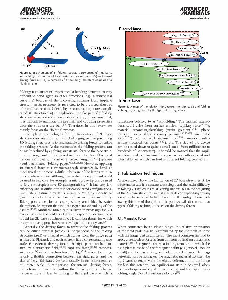
Folding usually refers to a process that changes the relative angle of two flat parts by deforming the joint between them, as illustrated in Figure 1a. The folding structure contains two parts: the rigid part (blue) and the hinge part (red). The rigid parts are flat plates that ideally undergo no shape deformation during the folding process, and the hinge parts are the con-nections between the rigid parts that undergo plastic or elastic deformations. When a driving force from either external (out-side of the hinge) or internal (within the hinge) is applied, shape deformation of the hinge parts occurs to alter the relative orientation of the rigid parts, resulting in the 3D folded struc-tures. In comparison, another process that is quite similar to
“folding” is called “bending” (illustrated in Figure 1b), which should be distinguished carefully. In this process, the whole structure is deformed compared to the folding process where only the hinge part curves. It can be realized in almost the same way that we did on the folding ones—a driving force is applied on a nonrigid film. However, it has two drawbacks compared to
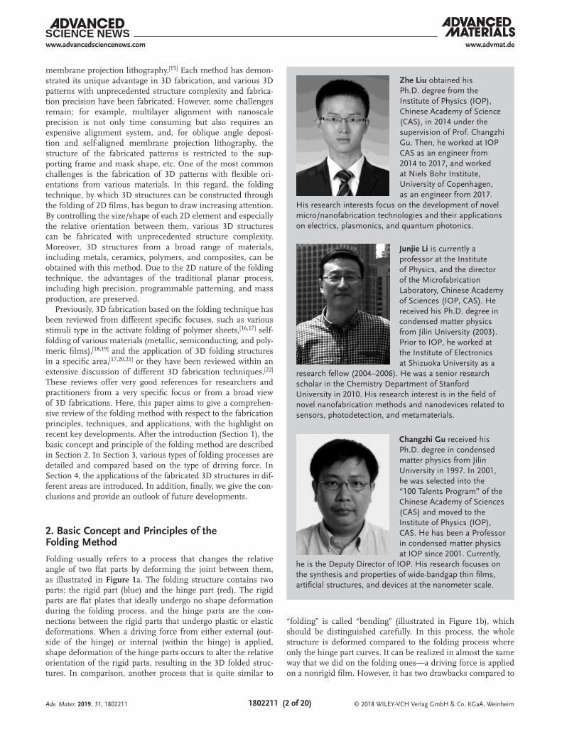
Zhe Liu obtained his Ph.D. degree from the Institute of Physics (IOP), Chinese Academy of Science (CAS), in 2014 under the supervision of Prof. Changzhi Gu. Then, he worked at IOP CAS as an engineer from 2014 to 2017, and worked at Niels Bohr Institute, University of Copenhagen, as an engineer from 2017.
His research interests focus on the development of novel micro/nanofabrication technologies and their applications on electrics, plasmonics, and quantum photonics.
Junjie Li is currently a professor at the Institute of Physics, and the director of the Microfabrication Laboratory, Chinese Academy of Sciences (IOP, CAS). He received his Ph.D. degree in condensed matter physics from Jilin University (2003). Prior to IOP, he worked at the Institute of Electronics at Shizuoka University as a
research fellow (2004–2006). He was a senior research scholar in the Chemistry Department of Stanford University in 2010. His research interest is in the field of novel nanofabrication methods and nanodevices related to sensors, photodetection, and metamaterials.
Changzhi Gu received his Ph.D. degree in condensed matter physics from Jilin University in 1997. In 2001, he was selected into the “100 Talents Program” of the Chinese Academy of Sciences (CAS) and moved to the Institute of Physics (IOP), CAS. He has been a Professor in condensed matter physics at IOP since 2001. Currently,
he is the Deputy Director of IOP. His research focuses on the synthesis and properties of wide-bandgap thin films, artificial structures, and devices at the nanometer scale.
Adv. Mater. 2019, 31, 1802211
© 2018 WILEY-VCH Verlag GmbH & Co. KGaA, Weinheim1802211 (3 of 20)
www.advmat.dewww.advancedsciencenews.com
folding: i) In structural mechanics, a bending structure is very difficult to bend again in other directions (e.g., a transversal curvature) because of the increasing stiffness from in-plane stress,[23] so its geometry is restricted to be a curved sheet or tube and has restricted flexibility in constructing more compli-cated 3D structures. ii) In application, the flat part of a folding structure is necessary in many devices; e.g., in metamaterial, it is difficult to maintain the intrinsic and coupling properties once the structures are bent.[24] Therefore, in this review, we mainly focus on the “folding” process.
Since planar technologies for the fabrication of 2D base structures are mature, the most challenging part in producing 3D folding structures is to find suitable driving forces to realize the folding process. At the macroscale, the folding process can be easily realized by applying an external force to the base struc-ture by using hand or mechanical instruments. One of the most famous examples is the artware named “origami,” a Japanese word that means “folding paper.”[16,20,25,26] However, applying an external force to a micro/nanoscale structure by hand or mechanical equipment is difficult because of the large size mis-match between them. Although some delicate equipment could be used in this case, for example, a microprobe tip can be used to fold a microplate into 3D configurations,[27] it has very low efficiency and is difficult to use for complicated configurations. Fortunately, nature provides a variety of “folding models” to give us a clue that there are other approaches to realize folding. Taking pine cones for an example, they are folded by water absorption/desorption that induces expansion/shrinking of the tissues.[19,28] Similarly, much care is taken to predesign the 2D base structures and find a suitable corresponding driving force to fold the 2D base structures into 3D configurations, for which many creative approaches were developed in recent years.[29]
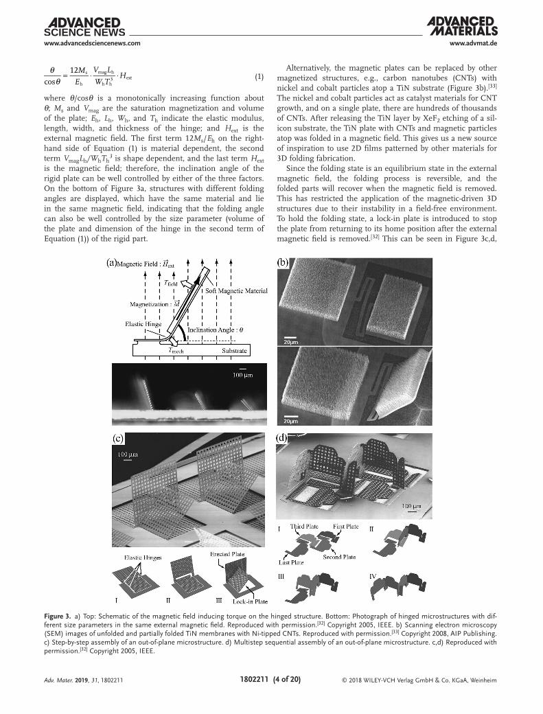
Generally, the driving forces to activate the folding process can be either external (which is independent of the folding structure itself) or internal (which comes from the hinge part) as listed in Figure 2, and each strategy has a corresponding size scale. For external driving forces, the rigid parts can be actu-ated by a magnetic field,[30–33] capillary force,[34,35] compres-sive force,[36] or cell traction force (CTF),[37,38] where the hinge is only a flexible connection between the rigid parts, and the size of the as-fabricated device is usually in the micrometer or millimeter scale. In comparison, for internal driving forces, the internal interactions within the hinge part can change its curvature and lead to folding of the rigid parts, which is
sometimes referred to as “self-folding.” The internal interac-tions could arise from surface tension (capillary force[39–64]), material expansion/shrinking (strain gradient,[52–64] phase transition in a shape memory polymer,[25,65–71] pneumatic force[72,73]), bio-force (cell traction force[37,38]), ion–solid inter-actions (focused ion beam[74–87]), etc. The size of the device can be scaled down to quite a small scale (from millimeters to hundreds of nanometers). It should be noticed that the capil-lary force and cell traction force can act as both external and internal forces, which can lead to different folding behaviors.
3. Fabrication Techniques
As mentioned above, the fabrication of 2D base structures at the micro/nanoscale is a mature technology, and the main difficulty in folding 2D structures to 3D configurations lies in the designing of the 2D base structures so that a suitable corresponding driving force can be activated to fold them into 3D configurations. Fol-lowing this line of thought, in this part, we will discuss various types of folding techniques based on the driving forces.
3.1. Magnetic Force
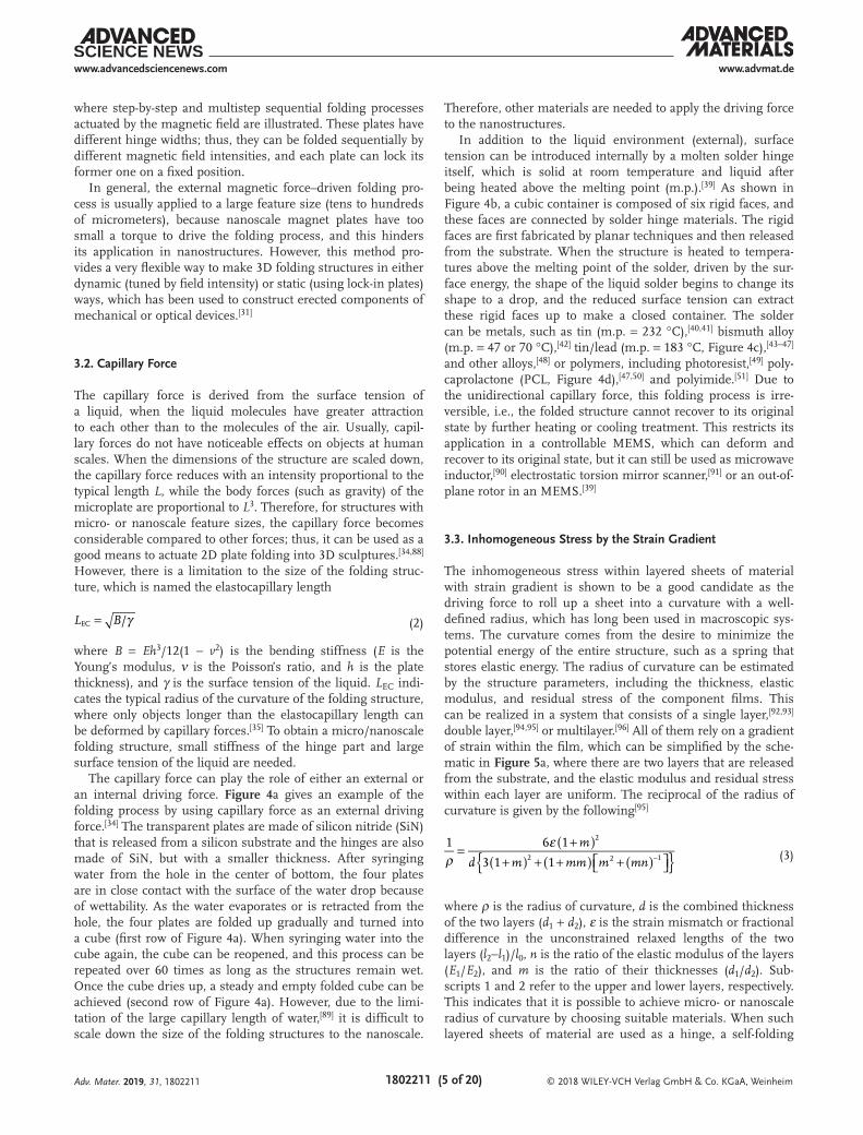
When connected by an elastic hinge, the relative orientation of the rigid parts can be manipulated by the moment of force with the hinge part as a fulcrum. The most common method to apply a contactless force is from a magnetic field on a magnetic material.[30–32] Figure 3a shows a folding structure in which the rigid plate is made of a soft magnetic film (e.g., nickel, iron, or cobalt) and the elastic hinge is made of a nickel layer. The mag-netostatic torque acting on the magnetic material actuates the rigid parts to rotate while the elastic deformation of the hinge hinders this rotation. An equilibrium state is achieved when the two torques are equal to each other, and the equilibrium folding angle θ can be written as follows[32]
Adv. Mater. 2019, 31, 1802211
Figure 1. a) Schematic of a “folding” structure composed of rigid parts and a hinge part actuated by an external driving force (FE) or internal driving force (FI). b) Schematic of a “bending” structure compared to “folding” one.
Figure 2. A map of the relationship between the size scale and folding techniques, categorized by the types of driving forces.
© 2018 WILEY-VCH Verlag GmbH & Co. KGaA, Weinheim1802211 (4 of 20)
www.advmat.dewww.advancedsciencenews.com
M
E
V L
W TH
cos12 s
h
mag h
h h3 ext
θθ
= ⋅ ⋅ (1)
where θ/cosθ is a monotonically increasing function about θ; Ms and Vmag are the saturation magnetization and volume of the plate; Eh, Lh, Wh, and Th indicate the elastic modulus, length, width, and thickness of the hinge; and Hext is the external magnetic field. The first term 12Ms/Eh on the right-hand side of Equation (1) is material dependent, the second term VmagLh/WhTh
3 is shape dependent, and the last term Hext is the magnetic field; therefore, the inclination angle of the rigid plate can be well controlled by either of the three factors. On the bottom of Figure 3a, structures with different folding angles are displayed, which have the same material and lie in the same magnetic field, indicating that the folding angle can also be well controlled by the size parameter (volume of the plate and dimension of the hinge in the second term of Equation (1)) of the rigid part.
Alternatively, the magnetic plates can be replaced by other magnetized structures, e.g., carbon nanotubes (CNTs) with nickel and cobalt particles atop a TiN substrate (Figure 3b).[33] The nickel and cobalt particles act as catalyst materials for CNT growth, and on a single plate, there are hundreds of thousands of CNTs. After releasing the TiN layer by XeF2 etching of a sil-icon substrate, the TiN plate with CNTs and magnetic particles atop was folded in a magnetic field. This gives us a new source of inspiration to use 2D films patterned by other materials for 3D folding fabrication.
Since the folding state is an equilibrium state in the external magnetic field, the folding process is reversible, and the folded parts will recover when the magnetic field is removed. This has restricted the application of the magnetic-driven 3D structures due to their instability in a field-free environment. To hold the folding state, a lock-in plate is introduced to stop the plate from returning to its home position after the external magnetic field is removed.[32] This can be seen in Figure 3c,d,
Adv. Mater. 2019, 31, 1802211
Figure 3. a) Top: Schematic of the magnetic field inducing torque on the hinged structure. Bottom: Photograph of hinged microstructures with dif-ferent size parameters in the same external magnetic field. Reproduced with permission.[32] Copyright 2005, IEEE. b) Scanning electron microscopy (SEM) images of unfolded and partially folded TiN membranes with Ni-tipped CNTs. Reproduced with permission.[33] Copyright 2008, AIP Publishing. c) Step-by-step assembly of an out-of-plane microstructure. d) Multistep sequential assembly of an out-of-plane microstructure. c,d) Reproduced with permission.[32] Copyright 2005, IEEE.
© 2018 WILEY-VCH Verlag GmbH & Co. KGaA, Weinheim1802211 (5 of 20)
www.advmat.dewww.advancedsciencenews.com
where step-by-step and multistep sequential folding processes actuated by the magnetic field are illustrated. These plates have different hinge widths; thus, they can be folded sequentially by different magnetic field intensities, and each plate can lock its former one on a fixed position.
In general, the external magnetic force–driven folding pro-cess is usually applied to a large feature size (tens to hundreds of micrometers), because nanoscale magnet plates have too small a torque to drive the folding process, and this hinders its application in nanostructures. However, this method pro-vides a very flexible way to make 3D folding structures in either dynamic (tuned by field intensity) or static (using lock-in plates) ways, which has been used to construct erected components of mechanical or optical devices.[31]
3.2. Capillary Force
The capillary force is derived from the surface tension of a liquid, when the liquid molecules have greater attraction to each other than to the molecules of the air. Usually, capil-lary forces do not have noticeable effects on objects at human scales. When the dimensions of the structure are scaled down, the capillary force reduces with an intensity proportional to the typical length L, while the body forces (such as gravity) of the microplate are proportional to L3. Therefore, for structures with micro- or nanoscale feature sizes, the capillary force becomes considerable compared to other forces; thus, it can be used as a good means to actuate 2D plate folding into 3D sculptures.[34,88] However, there is a limitation to the size of the folding struc-ture, which is named the elastocapillary length
L B/EC γ= (2)
where B = Eh3/12(1 − v2) is the bending stiffness (E is the Young’s modulus, ν is the Poisson’s ratio, and h is the plate thickness), and γ is the surface tension of the liquid. LEC indi-cates the typical radius of the curvature of the folding structure, where only objects longer than the elastocapillary length can be deformed by capillary forces.[35] To obtain a micro/nanoscale folding structure, small stiffness of the hinge part and large surface tension of the liquid are needed.
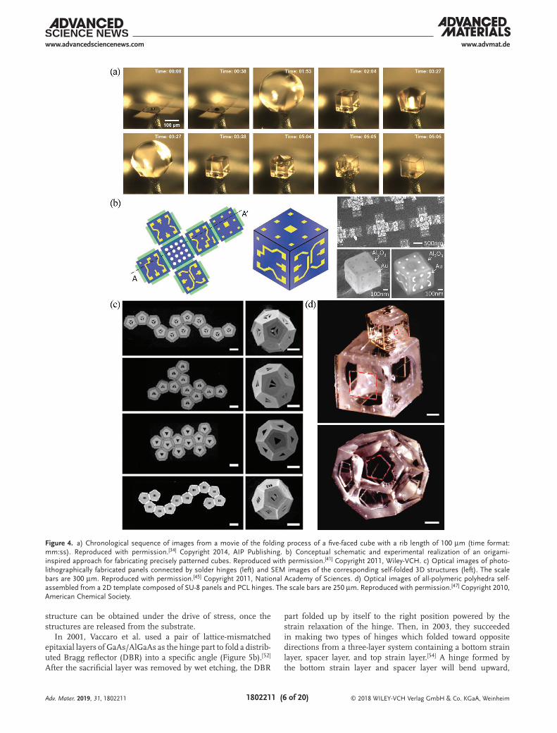
The capillary force can play the role of either an external or an internal driving force. Figure 4a gives an example of the folding process by using capillary force as an external driving force.[34] The transparent plates are made of silicon nitride (SiN) that is released from a silicon substrate and the hinges are also made of SiN, but with a smaller thickness. After syringing water from the hole in the center of bottom, the four plates are in close contact with the surface of the water drop because of wettability. As the water evaporates or is retracted from the hole, the four plates are folded up gradually and turned into a cube (first row of Figure 4a). When syringing water into the cube again, the cube can be reopened, and this process can be repeated over 60 times as long as the structures remain wet. Once the cube dries up, a steady and empty folded cube can be achieved (second row of Figure 4a). However, due to the limi-tation of the large capillary length of water,[89] it is difficult to scale down the size of the folding structures to the nanoscale.
Therefore, other materials are needed to apply the driving force to the nanostructures.
In addition to the liquid environment (external), surface tension can be introduced internally by a molten solder hinge itself, which is solid at room temperature and liquid after being heated above the melting point (m.p.).[39] As shown in Figure 4b, a cubic container is composed of six rigid faces, and these faces are connected by solder hinge materials. The rigid faces are first fabricated by planar techniques and then released from the substrate. When the structure is heated to tempera-tures above the melting point of the solder, driven by the sur-face energy, the shape of the liquid solder begins to change its shape to a drop, and the reduced surface tension can extract these rigid faces up to make a closed container. The solder can be metals, such as tin (m.p. = 232 °C),[40,41] bismuth alloy (m.p. = 47 or 70 °C),[42] tin/lead (m.p. = 183 °C, Figure 4c),[43–47] and other alloys,[48] or polymers, including photoresist,[49] poly-caprolactone (PCL, Figure 4d),[47,50] and polyimide.[51] Due to the unidirectional capillary force, this folding process is irre-versible, i.e., the folded structure cannot recover to its original state by further heating or cooling treatment. This restricts its application in a controllable MEMS, which can deform and recover to its original state, but it can still be used as microwave inductor,[90] electrostatic torsion mirror scanner,[91] or an out-of-plane rotor in an MEMS.[39]
3.3. Inhomogeneous Stress by the Strain Gradient
The inhomogeneous stress within layered sheets of material with strain gradient is shown to be a good candidate as the driving force to roll up a sheet into a curvature with a well-defined radius, which has long been used in macroscopic sys-tems. The curvature comes from the desire to minimize the potential energy of the entire structure, such as a spring that stores elastic energy. The radius of curvature can be estimated by the structure parameters, including the thickness, elastic modulus, and residual stress of the component films. This can be realized in a system that consists of a single layer,[92,93] double layer,[94,95] or multilayer.[96] All of them rely on a gradient of strain within the film, which can be simplified by the sche-matic in Figure 5a, where there are two layers that are released from the substrate, and the elastic modulus and residual stress within each layer are uniform. The reciprocal of the radius of curvature is given by the following[95]
m
d m mm m mn
1 6 1
3 1 1
2
2 2 1ρε
{ }( )
( ) ( ) ( )= +
+ + + + − (3)
where ρ is the radius of curvature, d is the combined thickness of the two layers (d1 + d2), ε is the strain mismatch or fractional difference in the unconstrained relaxed lengths of the two layers (l2−l1)/l0, n is the ratio of the elastic modulus of the layers (E1/E2), and m is the ratio of their thicknesses (d1/d2). Sub-scripts 1 and 2 refer to the upper and lower layers, respectively. This indicates that it is possible to achieve micro- or nanoscale radius of curvature by choosing suitable materials. When such layered sheets of material are used as a hinge, a self-folding
Adv. Mater. 2019, 31, 1802211
© 2018 WILEY-VCH Verlag GmbH & Co. KGaA, Weinheim1802211 (6 of 20)
www.advmat.dewww.advancedsciencenews.com
structure can be obtained under the drive of stress, once the structures are released from the substrate.
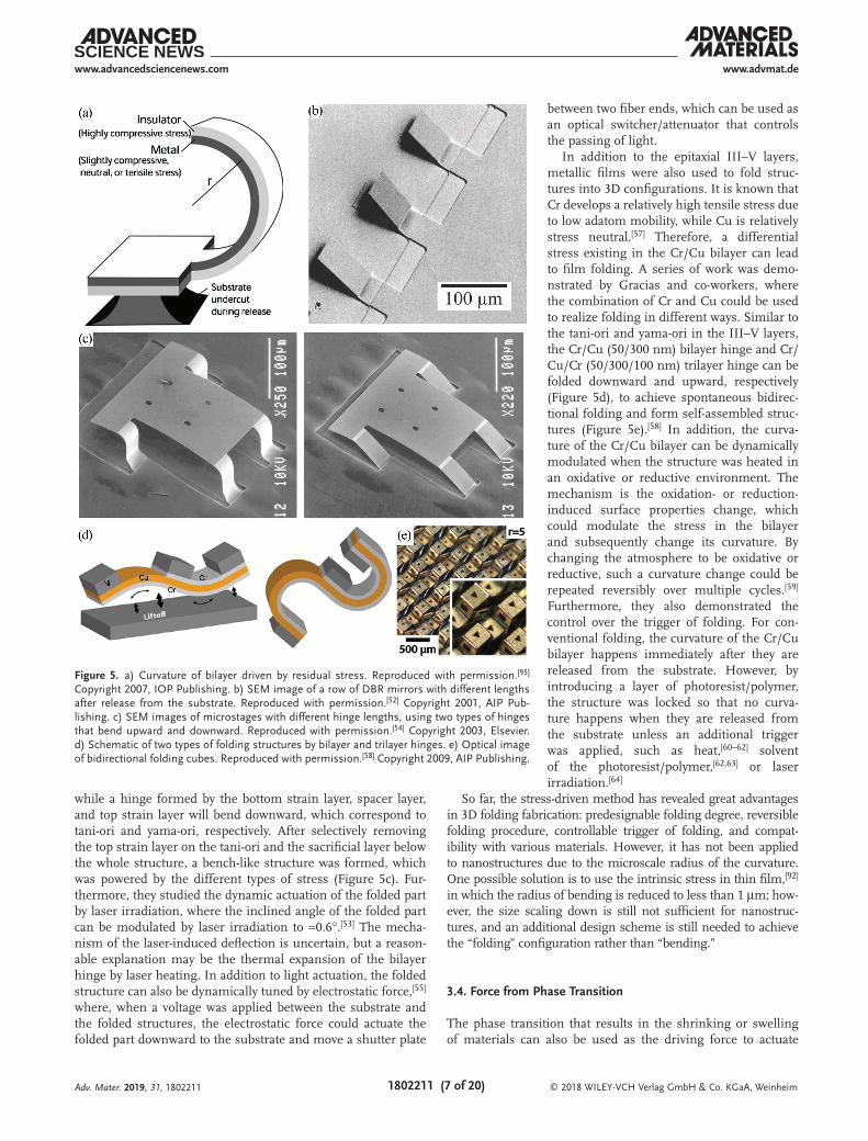
In 2001, Vaccaro et al. used a pair of lattice-mismatched epitaxial layers of GaAs/AlGaAs as the hinge part to fold a distrib-uted Bragg reflector (DBR) into a specific angle (Figure 5b).[52] After the sacrificial layer was removed by wet etching, the DBR
part folded up by itself to the right position powered by the strain relaxation of the hinge. Then, in 2003, they succeeded in making two types of hinges which folded toward opposite directions from a three-layer system containing a bottom strain layer, spacer layer, and top strain layer.[54] A hinge formed by the bottom strain layer and spacer layer will bend upward,
Adv. Mater. 2019, 31, 1802211
Figure 4. a) Chronological sequence of images from a movie of the folding process of a five-faced cube with a rib length of 100 µm (time format: mm:ss). Reproduced with permission.[34] Copyright 2014, AIP Publishing. b) Conceptual schematic and experimental realization of an origami-inspired approach for fabricating precisely patterned cubes. Reproduced with permission.[41] Copyright 2011, Wiley-VCH. c) Optical images of photo-lithographically fabricated panels connected by solder hinges (left) and SEM images of the corresponding self-folded 3D structures (left). The scale bars are 300 µm. Reproduced with permission.[45] Copyright 2011, National Academy of Sciences. d) Optical images of all-polymeric polyhedra self-assembled from a 2D template composed of SU-8 panels and PCL hinges. The scale bars are 250 µm. Reproduced with permission.[47] Copyright 2010, American Chemical Society.
© 2018 WILEY-VCH Verlag GmbH & Co. KGaA, Weinheim1802211 (7 of 20)
www.advmat.dewww.advancedsciencenews.com
while a hinge formed by the bottom strain layer, spacer layer, and top strain layer will bend downward, which correspond to tani-ori and yama-ori, respectively. After selectively removing the top strain layer on the tani-ori and the sacrificial layer below the whole structure, a bench-like structure was formed, which was powered by the different types of stress (Figure 5c). Fur-thermore, they studied the dynamic actuation of the folded part by laser irradiation, where the inclined angle of the folded part can be modulated by laser irradiation to ≈0.6°.[53] The mecha-nism of the laser-induced deflection is uncertain, but a reason-able explanation may be the thermal expansion of the bilayer hinge by laser heating. In addition to light actuation, the folded structure can also be dynamically tuned by electrostatic force,[55] where, when a voltage was applied between the substrate and the folded structures, the electrostatic force could actuate the folded part downward to the substrate and move a shutter plate
between two fiber ends, which can be used as an optical switcher/attenuator that controls the passing of light.
In addition to the epitaxial III–V layers, metallic films were also used to fold struc-tures into 3D configurations. It is known that Cr develops a relatively high tensile stress due to low adatom mobility, while Cu is relatively stress neutral.[57] Therefore, a differential stress existing in the Cr/Cu bilayer can lead to film folding. A series of work was demo-nstrated by Gracias and co-workers, where the combination of Cr and Cu could be used to realize folding in different ways. Similar to the tani-ori and yama-ori in the III–V layers, the Cr/Cu (50/300 nm) bilayer hinge and Cr/Cu/Cr (50/300/100 nm) trilayer hinge can be folded downward and upward, respectively (Figure 5d), to achieve spontaneous bidirec-tional folding and form self-assembled struc-tures (Figure 5e).[58] In addition, the curva-ture of the Cr/Cu bilayer can be dynamically modulated when the structure was heated in an oxidative or reductive environment. The mechanism is the oxidation- or reduction-induced surface properties change, which could modulate the stress in the bilayer and subsequently change its curvature. By changing the atmosphere to be oxidative or reductive, such a curvature change could be repeated reversibly over multiple cycles.[59] Furthermore, they also demonstrated the control over the trigger of folding. For con-ventional folding, the curvature of the Cr/Cu bilayer happens immediately after they are released from the substrate. However, by introducing a layer of photoresist/polymer, the structure was locked so that no curva-ture happens when they are released from the substrate unless an additional trigger was applied, such as heat,[60–62] solvent of the photo resist/polymer,[62,63] or laser irradiation.[64]
So far, the stress-driven method has revealed great advantages in 3D folding fabrication: predesignable folding degree, reversible folding procedure, controllable trigger of folding, and compat-ibility with various materials. However, it has not been applied to nanostructures due to the microscale radius of the curvature. One possible solution is to use the intrinsic stress in thin film,[92] in which the radius of bending is reduced to less than 1 µm; how-ever, the size scaling down is still not sufficient for nanostruc-tures, and an additional design scheme is still needed to achieve the “folding” configuration rather than “bending.”
3.4. Force from Phase Transition
The phase transition that results in the shrinking or swelling of materials can also be used as the driving force to actuate
Adv. Mater. 2019, 31, 1802211
Figure 5. a) Curvature of bilayer driven by residual stress. Reproduced with permission.[95] Copyright 2007, IOP Publishing. b) SEM image of a row of DBR mirrors with different lengths after release from the substrate. Reproduced with permission.[52] Copyright 2001, AIP Pub-lishing. c) SEM images of microstages with different hinge lengths, using two types of hinges that bend upward and downward. Reproduced with permission.[54] Copyright 2003, Elsevier. d) Schematic of two types of folding structures by bilayer and trilayer hinges. e) Optical image of bidirectional folding cubes. Reproduced with permission.[58] Copyright 2009, AIP Publishing.
© 2018 WILEY-VCH Verlag GmbH & Co. KGaA, Weinheim1802211 (8 of 20)
www.advmat.dewww.advancedsciencenews.com
the movement of structures, where a shape memory polymer (SMP) is a good candidate for the folding process. SMPs[97] are materials that have the ability to return from temporary shapes to their permanent shape upon exposure to an external stimulus, such as heat,[98] light,[99] moisture,[100] or magnetic field,[101] with shrinking or swelling of the polymer. The origin of the deformation lies in the different molecular network structure from different phases. When the hinge parts are made of SMPs, a folding process can be activated if the SMPs return to their original shape.
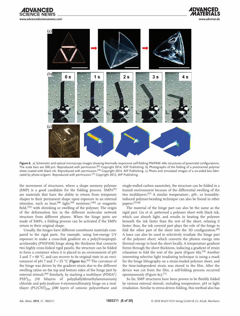
Usually, the hinges have different constituent materials com-pared to the rigid parts. For example, using low-energy UV exposure to make a cross-link gradient on a poly(N-isopropyl-acrylamide) (PNIPAM) hinge along the thickness that connects two highly cross-linked rigid panels, the structure can be folded to form a container when it is placed in an environment of pH 2 and T = 60 °C, and can recover to its original state in an envi-ronment of pH 7 and T = 25 °C (Figure 6a).[65] The curvature of the hinge was driven by the gradient strain due to the different swelling ratios on the top and bottom sides of the hinge part by external stimuli.[66] Similarly, by stacking a multilayer (PDDA2/PSS2)10 (10 bilayers of poly(diallyldimethylammonium) chloride and poly-(sodium 4-styrenesulfonate)) hinge on a mul-tilayer (PU/CNT)200 (200 layers of cationic polyurethane and
single-walled carbon nanotube), the structure can be folded in a humid environment because of the differential swelling of the two multilayers.[67] A similar temperature-, pH-, or humidity-induced polymer-bending technique can also be found in other papers.[25,68]
The material of the hinge part can also be the same as the rigid part. Liu et al. patterned a polymer sheet with black ink, which can absorb light, and results in heating the polymer beneath the ink faster than the rest of the sheet, relaxing it faster; thus, the ink covered part plays the role of the hinge to fold the other part of the sheet into the 3D configuration.[69] A laser can also be used to selectively irradiate the hinge part of the polymer sheet, which converts the photon energy into thermal energy to heat the sheet locally. A temperature gradient forms through the sheet thickness, inducing a gradient of strain relaxation to fold the rest of the parts (Figure 6b).[70] Another interesting selective light irradiating technique is using a mask for the hinge lithography on a strain-loaded polymer sheet, and the time-independent strain was stored in the film. After the device was cut from the film, a self-folding process occurred spontaneously (Figure 6c).[71]
So far, SMP structures have been proven to be flexibly folded by various external stimuli, including temperature, pH or light irradiation. Similar to stress-driven folding, this method also has
Adv. Mater. 2019, 31, 1802211
Figure 6. a) Schematic and optical microscopy images showing thermally responsive self-folding PNIPAM–AAc structures of pyramidal configurations. The scale bars are 300 µm. Reproduced with permission.[65] Copyright 2014, IOP Publishing. b) Photographs of the folding of a prestrained polymer sheet coated with black ink. Reproduced with permission.[70] Copyright 2014, AIP Publishing. c) Photo and simulated images of a six-sided box fabri-cated by photo-origami. Reproduced with permission.[71] Copyright 2012, AIP Publishing.
© 2018 WILEY-VCH Verlag GmbH & Co. KGaA, Weinheim1802211 (9 of 20)
www.advmat.dewww.advancedsciencenews.com
the advantage of a reversible folding procedure and a control-lable trigger of folding, making the 3D polymer structures good candidates for dynamic or programmable-assembly devices. However, due to the fabrication resolution of the rigid and hinge parts, the 3D polymer structures have not been achieved at the nanoscale, so more effort is needed in the future.
3.5. Force from Ion–Solid Interactions
In addition to the materials within the structures, additional materials (e.g., energetic ions) can be introduced to modify
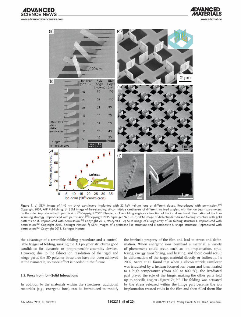
the intrinsic property of the film and lead to stress and defor-mation. When energetic ions bombard a material, a variety of phenomena could occur, such as ion implantation, sput-tering, energy transferring, and heating, and these could result in deformation of the target material directly or indirectly. In 2007, Arora et al. found that when a silicon nitride cantilever was irradiated by a helium focused ion beam and then heated to a high temperature (from 400 to 800 °C), the irradiated part played the role of the hinge, making the other parts fold up to specific angles (Figure 7a).[74] The folding was actuated by the stress released within the hinge part because the ion implantation created voids in the film and then filled them like
Adv. Mater. 2019, 31, 1802211
Figure 7. a) SEM image of 140 nm thick cantilevers implanted with 22 keV helium ions at different doses. Reproduced with permission.[74] Copyright 2007, AIP Publishing. b) SEM image of free-standing silicon nitride cantilevers of different inclined angles, with the ion beam parameters on the side. Reproduced with permission.[76] Copyright 2007, Elsevier. c) The folding angle as a function of the ion dose. Inset: Illustration of the line-scanning strategy. Reproduced with permission.[82] Copyright 2015, Springer Nature. d) SEM image of dielectric-film-based folding structure with gold patterns on it. Reproduced with permission.[86] Copyright 2017, Wiley-VCH. e) SEM image of a large array of 3D folding structures. Reproduced with permission.[82] Copyright 2015, Springer Nature. f) SEM images of a staircase-like structure and a composite U-shape structure. Reproduced with permission.[82] Copyright 2015, Springer Nature.
© 2018 WILEY-VCH Verlag GmbH & Co. KGaA, Weinheim1802211 (10 of 20)
www.advmat.dewww.advancedsciencenews.com
pressurized bubbles, causing compressive stress.[75] Instead of using the combination of helium focused ion beam irradiation and heating, another way to fold a cantilever was demonstrated later, where a Ga focused ion beam irradiation only could induce folding directly.[76] Figure 7b shows the folding of a SiN cantilever (coated with 3 nm of gold to prevent charging) with the focused ion beam irradiated part acting as a hinge. More-over, a positive correlation between the folding angle and the ion beam dose was identified.
Many experiments were carried out afterward to study the interaction between energetic ions and the target using dif-ferent ion species and different energies on various target mate-rials. Different bending phenomena were observed and various mechanisms were proposed including the following: i) ion-implantation-induced voids and, hence, compressive stress;[74,77] ii) ion-implantation-induced compressive and tensile stress by interstitial and vacancy defects;[76,78] iii) ions deposited on the surface;[76] iv) high-energy implantation resulting in tempera-ture increasing and material melting on the surface;[79] and v) mass transport to the surface of the material caused by ener-getic ion bombardment.[80] Based on these studies, a fabrication strategy can be extracted to fold 1D/2D structures into 3D at the micro/nanoscale.
In our group, we systematically studied the effect of the ion beam direction, ion beam dose, and substrate conductivity on the folding phenomena of nanowires and cantilevers.[81–85] The folding behavior of the Au cantilever under the Ga focused ion beam was identified: (1) when part of the Au cantilever is irradi-ated, the free part will fold toward the ion beam with the irradiated part acting as a hinge, as shown in the inset of Figure 7c. (2) The folding angle is almost proportional to ion dose until the free part of the cantilever is parallel with the ion beam (Figure 7c). (3) A folding angle from 0° to 180° to any direction can be realized by adjusting the related parameters, including the direction/angle of the ion beam and ion dose. Compared to Au-film-based structures, using a focused ion beam to fold dielectric-film-based structures in a highly controllable way is challenging because of the charging effect of the ions. To solve this problem, we have developed a revised fabrication method by combing a sacrificial conduc-tive layer with the dielectric film before folding them into 3D structures, and then removing the sacrificial conductive layer by chemical etching. Therefore, we can fold the dielectric-film-based structures in the same way as the Au-film-based structures while making metal patterns on the vertical films (Figure 7d).[86]
Based on these phenomena and by designing the shape of the 2D components, various 3D structures can be fabricated with high uniformity/consistency across a sufficiently large area, e.g., on the order of square millimeters (Figure 7e). More-over, the focused ion beam is a serial technology with advanced functionalities that can be used not only to pattern the 2D components but also to design the irradiation order/sequence, making the fabrication of 3D structures with complicated con-figuration possible, as shown in Figure 7f, which is difficult to fabricate by other technologies.
The focused ion beam is a micro/nanofabrication technique using the nanoscale ion beam spot, with nanoscale precision, des-ignable patterning ability, and high fabrication uniformity over a large area, making it very suitable for 3D folding fabrication. 3D structures composed of various materials (metal, dielectric,
and semiconductor) in a broad range of sizes (from nano-meter to millimeter) have been fabricated. However, the inter-action between the energetic ions and the target materials could change the properties of the material by inducing an ion beam irradiation effect; thus, it should be taken into considera-tion under certain circumstance. Another disadvantage is that it is a serial technology with a spot-by-spot scanning strategy, making the fabrication process less time efficient than parallel processes (e.g., optical lithography and nanoimprinting can acquire patterns of large areas in a single lithography step).
3.6. Other Techniques
In addition to the abovementioned folding techniques, there are still other interesting methods to make 3D folding struc-tures, which may not be as widely used as the abovementioned methods, but still inspire creativity in this area.
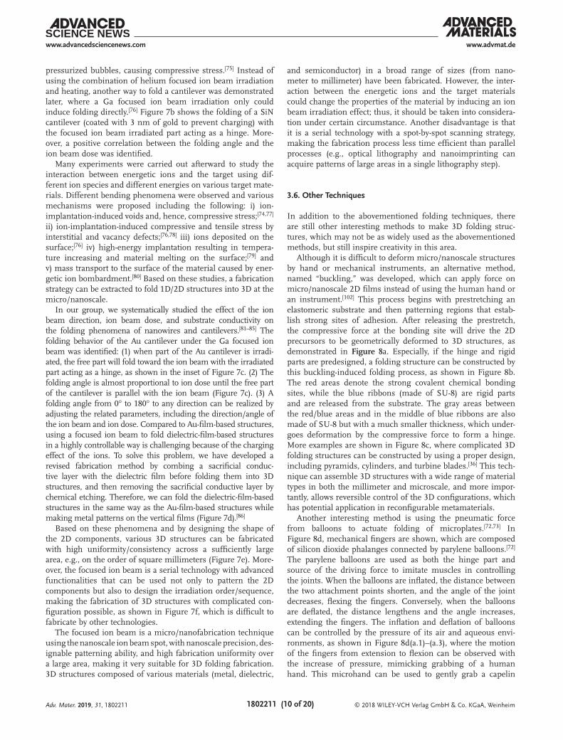
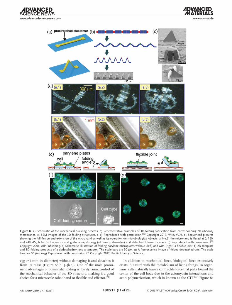
Although it is difficult to deform micro/nanoscale structures by hand or mechanical instruments, an alternative method, named “buckling,” was developed, which can apply force on micro/nanoscale 2D films instead of using the human hand or an instrument.[102] This process begins with prestretching an elastomeric substrate and then patterning regions that estab-lish strong sites of adhesion. After releasing the prestretch, the compressive force at the bonding site will drive the 2D precursors to be geometrically deformed to 3D structures, as demonstrated in Figure 8a. Especially, if the hinge and rigid parts are predesigned, a folding structure can be constructed by this buckling-induced folding process, as shown in Figure 8b. The red areas denote the strong covalent chemical bonding sites, while the blue ribbons (made of SU-8) are rigid parts and are released from the substrate. The gray areas between the red/blue areas and in the middle of blue ribbons are also made of SU-8 but with a much smaller thickness, which under-goes deformation by the compressive force to form a hinge. More examples are shown in Figure 8c, where complicated 3D folding structures can be constructed by using a proper design, including pyramids, cylinders, and turbine blades.[36] This tech-nique can assemble 3D structures with a wide range of material types in both the millimeter and microscale, and more impor-tantly, allows reversible control of the 3D configurations, which has potential application in reconfigurable metamaterials.
Another interesting method is using the pneumatic force from balloons to actuate folding of microplates.[72,73] In Figure 8d, mechanical fingers are shown, which are composed of silicon dioxide phalanges connected by parylene balloons.[72] The parylene balloons are used as both the hinge part and source of the driving force to imitate muscles in controlling the joints. When the balloons are inflated, the distance between the two attachment points shorten, and the angle of the joint decreases, flexing the fingers. Conversely, when the balloons are deflated, the distance lengthens and the angle increases, extending the fingers. The inflation and deflation of balloons can be controlled by the pressure of its air and aqueous envi-ronments, as shown in Figure 8d(a.1)–(a.3), where the motion of the fingers from extension to flexion can be observed with the increase of pressure, mimicking grabbing of a human hand. This microhand can be used to gently grab a capelin
Adv. Mater. 2019, 31, 1802211
© 2018 WILEY-VCH Verlag GmbH & Co. KGaA, Weinheim1802211 (11 of 20)
www.advmat.dewww.advancedsciencenews.com
egg (≈1 mm in diameter) without damaging it and detaches it from its mass (Figure 8d(b.1)–(b.3)). One of the most promi-nent advantages of pneumatic folding is the dynamic control of the mechanical behavior of the 3D structure, making it a good choice for a microscale robot hand or flexible end effector.[73]
In addition to mechanical force, biological force extensively exists in nature with the metabolism of living things. In organ-isms, cells naturally have a contractile force that pulls toward the center of the cell body due to the actomyosin interactions and actin polymerization, which is known as the CTF.[37] Figure 8e
Adv. Mater. 2019, 31, 1802211
Figure 8. a) Schematic of the mechanical buckling process. b) Representative examples of 3D folding fabrication from corresponding 2D ribbons/membranes. c) SEM images of the 3D folding structures. a–c) Reproduced with permission.[36] Copyright 2017, Wiley-VCH. d) Sequenced pictures showing the full flexion and extension of the microhand as well as its operation on microbiological objects: a.1–a.3) the microhand is flexed at 0, 160, and 240 kPa; b.1–b.3) the microhand grabs a capelin egg (≈1 mm in diameter) and detaches it from its mass. d) Reproduced with permission.[72] Copyright 2006, AIP Publishing. e) Schematic illustration of folding parylene microplates without (left) and with (right) a flexible joint. f) 2D template and 3D folding products of a dodecahedron and a tetragon. The scale bars are 50 µm. g) A fluorescence image of folded dodecahedrons. The scale bars are 50 µm. e–g) Reproduced with permission.[38] Copyright 2012, Public Library of Science.
© 2018 WILEY-VCH Verlag GmbH & Co. KGaA, Weinheim1802211 (12 of 20)
www.advmat.dewww.advancedsciencenews.com
shows two folding processes actuated by CTF, in which the hinge part is made of cells (therefore, the internal force in this case) or is not made of cells (external force in this case).[38] The rigid parts are made of parylene (poly(p-xylylene) polymer) microplates coated with fibronectin (FN). A sacrificial layer of gelatin is used to allow detachment of the rigid parts from the glass substrate. After the cells were successfully patterned onto the parylene microplates coated with FN, they adhered and stretched onto the plates. Then, the microplates were slightly pushed at their edges with a glass tip operated by a micromanip-ulator to trigger their detachment from the glass substrate. The detached microplate was pulled by the CTF generated by the cells cultured on the microplates until it can move no further. In the first case, when the cells play the role of the hinge, the folding angle can approximately be determined by the number of the cells on the microplates. The plate folded almost com-pletely when two or less cells bridged across two microplates, but with an increase in the number of cells, the microplates were blocked by the multiple cells and could not be folded fur-ther; thus, the folding angle decreased. In the other case, when there were hinges between the microplates, the folding process ended when the top inner edges of the two microplates con-nected to each other (Figure 8e, right). Figure 8f shows images of the 2D template and 3D folded product of a dodecahedron
and a tetragon, and Figure 8g shows a fluorescence image of many 3D dodecahedrons. This technique is quite time con-suming compared to other folding methods, which need tens of hours for cell culturing, but it still has great potential in making next-generation cell-based biohybrid medical devices due to its unique driving force from bio-tissue.
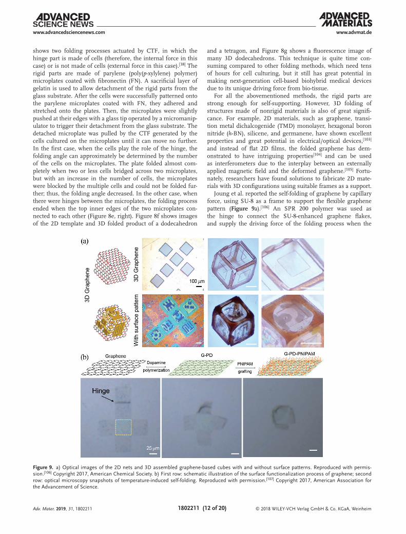
For all the abovementioned methods, the rigid parts are strong enough for self-supporting. However, 3D folding of structures made of nonrigid materials is also of great signifi-cance. For example, 2D materials, such as graphene, transi-tion metal dichalcogenide (TMD) monolayer, hexagonal boron nitride (h-BN), silicene, and germanene, have shown excellent properties and great potential in electrical/optical devices,[103] and instead of flat 2D films, the folded graphene has dem-onstrated to have intriguing properties[104] and can be used as interferometers due to the interplay between an externally applied magnetic field and the deformed graphene.[105] Fortu-nately, researchers have found solutions to fabricate 2D mate-rials with 3D configurations using suitable frames as a support.
Joung et al. reported the self-folding of graphene by capillary force, using SU-8 as a frame to support the flexible graphene pattern (Figure 9a).[106] An SPR 200 polymer was used as the hinge to connect the SU-8-enhanced graphene flakes, and supply the driving force of the folding process when the
Adv. Mater. 2019, 31, 1802211
Figure 9. a) Optical images of the 2D nets and 3D assembled graphene-based cubes with and without surface patterns. Reproduced with permis-sion.[106] Copyright 2017, American Chemical Society. b) First row: schematic illustration of the surface functionalization process of graphene; second row: optical microscopy snapshots of temperature-induced self-folding. Reproduced with permission.[107] Copyright 2017, American Association for the Advancement of Science.
© 2018 WILEY-VCH Verlag GmbH & Co. KGaA, Weinheim1802211 (13 of 20)
www.advmat.dewww.advancedsciencenews.com
sacrificial layer is removed and the temperature is above its melting point (≈100 °C). After removing the protection layer (Al2O3/Cr), which helps retain the physical and chemical prop-erties of graphene, a graphene-based self-assembled cube can finally be obtained. The 3D open and closed boxes generate highly confined electric fields due to plasmon–plasmon cou-pling at each of the faces and can be used as a sensor with high sensitivity to detect targeted substances while maintaining their integrity due to the impermeability of the graphene membranes.
Another strategy is using a polymer, named thermorespon-sive PNIPAM, to fold and unfold monolayer graphene into predesigned, ordered 3D structures (Figure 9b).[107] After func-tionalized on the surface of graphene and released from the substrate, the PNIPAM can fold the 2D sheets into ordered 3D microstructures by the molecular conformational change upon heating, while preserving the intrinsic properties of graphene (i.e., conductivity, doping, and transfer characteristics). The temperature responsiveness is reversible and can be widely uti-lized for actuators, sensors, and containers.
It should be pointed out that the two methods for graphene folding did not adopt new driving forces but made use of the capillary force or SMPs, as introduced above. However, it is a good method for folding flexible materials without damaging their intrinsic properties.
In summary, we can see that various folding technologies have been developed to fabricate 3D folding structures from micro-scopic to macroscopic sizes, and the constituent material covers almost all the material categories, including metal, ceramic, polymer, and composite materials. Each folding technique pos-sesses a unique feature in terms of the size scale, material type, and active capability due to the intrinsic property of the driving force; therefore, one can choose the most suitable driving force to construct the required folding structures. Meanwhile, people are looking forward to having more types of folding technologies in the future for the further functionalizing and miniaturizing of mechanic, electronic, or optic devices.
4. Applications
By applying the folding concept to micro/nanostructure design, many applications have been realized in not only art but also in biological, optical, and radiofrequency (RF) devices, which are reviewed in the following sections.
4.1. Controllable Drug Delivery
Traditional methods to deliver drugs into the human body are through physical digestion of medicine, intravenous and intramus-cular injections, eye drops, implants, suppositories, etc. However, these delivery systems are simple and usually follow first-order release kinetics, which lack consistency and uniformity of the drug dose.[108] The concept of sustained release was introduced in the 1960s,[109] which can modify the drug release profile in the body as needed and reduce the risk of toxic effects by attenuating the peaks and valleys of plasma drug concentrations. Microcontainers are a very good choice for the encapsulation and delivery of drugs, which can be fabricated by the abovementioned folding methods.[7,110]
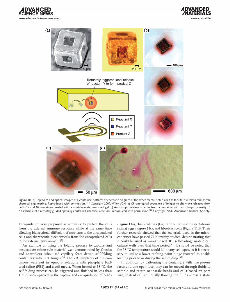
Gracias and co-workers succeeded in controlling chemical delivery remotely using self-folded containers and RF radia-tion.[111,112] The containers were made of Cu and Ni with iso-tropic porosity (Figure 10a), and they were filled with gel that was soaked in the chemical reagent to be released. Once loaded, the containers were placed in the desired location, guided by a magnetic stylus. To release the chemicals, an RF field generated by a 2D microcoil was directed toward the con-tainer. Through inductive coupling, eddy currents in the frame were induced and the container was heated by the Joule effect. Through heating, the gel encapsulated within the container was softened, resulting in the release of the chemicals. This method has several advantages in drug delivery. First, the heating of the container occurred only by inductive coupling, and the eddy currents could be made large enough to heat the containers from room temperature to ≈80 °C, showing a very high control-lability regarding when to release the drug. Second, by varying the porosity of the different faces of the container, isotropic release (Figure 10b) and anisotropic (Figure 10c) release were demonstrated. Moreover, a magnetic material, such as nickel, can be used for the rigid frame; thus, the container can be remotely guided using a magnetic field, making it possible to precisely control where to release the drug. Figure 10d shows the controllable moving of a container using a magnetic stylus, and the path of the container was controlled to write a letter “G.”[44] These studies prove the possibility of controlling when and where to release drugs, to administer therapeutics at the push of a button.
In addition to the static cubic container that does not deform during the therapy process, dynamic gripper-shaped containers called theragrippers were also applied for the sustained release of drugs,[113] which can close/open at different temperatures. The grippers are made of rigid poly(propylene fumarate) panels and flexible stimuli-responsive PNIPAM–AAc hinges. Due to the thermal responsiveness of the PNIPAM–AAc, they, origi-nally close at 4 °C, open as the solution temperature increases and finally close again in the opposite direction at 37 °C. The closing of the theragrippers at body temperature allows them to spontaneously grip onto tissue when introduced from a cold state into the body. Meanwhile, the theragrippers can load drugs into the body due to their porosity, and the drug elutes for over 7 days. The delivery of blue food dye into the esophagus of a pig by theragrippers was observed through an endoscope, proving it to be an effective strategy for sustained release of drugs with immediate applicability in the gastrointestinal tract. The folding technique shows good scaling capabilities from several microns[111] (small enough to be delivered to human vessel) to millimeters (which can work in the esophagus).[113]
4.2. Cell Encapsulation
In addition to fabricating containers to release chemicals or drugs, the 3D folding process can also be utilized to capture and encapsulate microscale objects, including cells, beads, or bacteria;[43,114] for example, it can be applied to a medical tech-nology named cell encapsulation therapy (CET). CET seeks to transplant exogenous cells to perform the function of diseased or damaged organs, an idea put forth in the mid 1970s.[115]
Adv. Mater. 2019, 31, 1802211
© 2018 WILEY-VCH Verlag GmbH & Co. KGaA, Weinheim1802211 (14 of 20)
www.advmat.dewww.advancedsciencenews.com
Encapsulation was proposed as a means to protect the cells from the external immune response while at the same time allowing bidirectional diffusion of nutrients to the encapsulated cells and therapeutic biochemicals from the encapsulated cells to the external environment.[7]
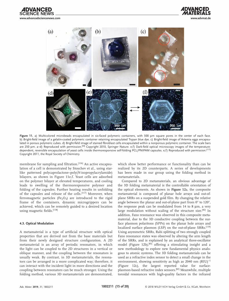
An example of using the folding process to capture and encapsulate microscale material was demonstrated by Gracias and co-workers, who used capillary force–driven self-folding containers with PCL hinges.[50] The 2D templates of the con-tainers were put in aqueous solutions with phosphate buff-ered saline (PBS) and a cell media. When heated to 58 °C, the self-folding process can be triggered and finished in less than 1 min, accompanied by the capture and encapsulation of beads
(Figure 11a), chemical dyes (Figure 11b), brine shrimp (Artemia salina) eggs (Figure 11c), and fibroblast cells (Figure 11d). Their further research showed that the materials used in the micro-container have passed 72 h toxicity studies, demonstrating that it could be used as miniaturized 3D, self-loading, mobile cell culture wells over that time period.[61] It should be noted that the 58 °C temperature would kill many cell types, so it is neces-sary to utilize a lower melting point hinge material to enable loading prior to or during the self-folding.[50]
In addition, by patterning the containers with five porous faces and one open face, they can be moved through fluids to sample and retain nanoscale beads and cells based on pore size, instead of traditionally flowing the fluids across a static
Adv. Mater. 2019, 31, 1802211
Figure 10. a) Top: SEM and optical images of a container; bottom: a schematic diagram of the experimental setup used to facilitate wireless microscale chemical engineering. Reproduced with permission.[111] Copyright 2007, Wiley-VCH. b) Chronological sequence of images to show dye released from both Cu and Ni containers loaded with a crystal-violet-dye-soaked gel. c) Anisotropic release of a dye from a container with anisotropic porosity. d) An example of a remotely guided spatially controlled chemical reaction. Reproduced with permission.[44] Copyright 2006, American Chemical Society.
© 2018 WILEY-VCH Verlag GmbH & Co. KGaA, Weinheim1802211 (15 of 20)
www.advmat.dewww.advancedsciencenews.com
Adv. Mater. 2019, 31, 1802211
membrane for sampling and filtration.[116] An active encapsu-lation of a cell is demonstrated by Stoychev et al., using star-like patterned polycaprolactone–poly(N-isopropylacrylamide) bilayers, as shown in Figure 11e,f. Yeast cells are adsorbed on the polymer bilayer at elevated temperatures, and cooling leads to swelling of the thermoresponsive polymer and folding of the capsules. Further heating results in unfolding of the capsules and release of the cells.[117] Moreover, when ferromagnetic particles (Fe2O3) are introduced to the rigid frame of the containers, dynamic microgrippers can be achieved, which can be remotely guided to a desired location using magnetic fields.[118]
4.3. Optical Modulation
A metamaterial is a type of artificial structure with optical properties that are derived not from the base materials but from their newly designed structure configuration. A 2D metamaterial is an array of periodic resonators, in which the light can be coupled to the 2D structures in a vertical or oblique manner, and the coupling between the resonators is usually weak. By contrast, in 3D metamaterials, the resona-tors can be arranged in a more complicated way; therefore, it can interact with the incident light in more directions and the coupling between resonators can be much stronger. Using the folding method, various 3D metamaterials are demonstrated,
which show better performance or functionality than can be realized by its 2D counterparts. A series of developments has been made in our group using the folding method in metamaterials.
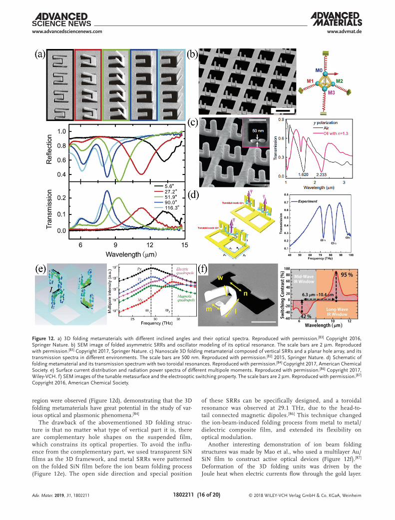
Compared to 2D metamaterials, an obvious advantage of the 3D folding metamaterial is the controllable orientation of the optical elements. As shown in Figure 12a, the composite metamaterial is composed of planar hole arrays and out-of-plane SRRs on a suspended gold film. By changing the relative angle between the planar and out-of-plane part from 0° to 120°, the response peak can be modulated from 14 to 8 µm, a very large modulation without scaling of the structure size.[82] In addition, Fano resonance was observed in this composite meta-material, due to the 3D conductive coupling between the sur-face plasmon polaritons (SPPs) on the planar hole arrays and localized surface plasmon (LSP) on the out-of-plane SRRs.[119] Using asymmetric SRRs, Rabi splitting of two strongly coupled Fano resonance states was observed by altering the arm length of the SRRs, and is explained by an analytical three-oscillator model (Figure 12b),[85] offering a stimulating insight and a new methodology to explore new fundamental physics analo-gous to atomic systems. The 3D folding metamaterials can be used as a refractive index sensor to detect a small change in the environment, showing sensitivity as high as 2040 nm (RIU)−1 (Figure 12c), the largest reported value for surface-plasmon-based refractive index sensors.[82] Meanwhile, multiple toroidal resonances with high-quality factors in the infrared
Figure 11. a) Multicolored microbeads encapsulated in six-faced polymeric containers, with 500 µm square pores in the center of each face. b) Bright-field image of a gelatin-coated polymeric container retaining encapsulated Trypan blue dye. c) Bright-field image of Artemia eggs encapsu-lated in porous polymeric cubes. d) Bright-field image of stained fibroblast cells encapsulated within a nonporous polymeric container. The scale bars are 250 µm. a–d) Reproduced with permission.[50] Copyright 2010, Springer Nature. e,f) Dark-field optical microscopy images of the temperature-dependent, reversible encapsulation of yeast cells inside thermoresponsive self-folding PCL/PNIPAM capsules. e,f) Reproduced with permission.[117] Copyright 2011, the Royal Society of Chemistry.
© 2018 WILEY-VCH Verlag GmbH & Co. KGaA, Weinheim1802211 (16 of 20)
www.advmat.dewww.advancedsciencenews.com
Adv. Mater. 2019, 31, 1802211
region were observed (Figure 12d), demonstrating that the 3D folding metamaterials have great potential in the study of var-ious optical and plasmonic phenomena.[84]
The drawback of the abovementioned 3D folding struc-ture is that no matter what type of vertical part it is, there are complementary hole shapes on the suspended film, which constrains its optical properties. To avoid the influ-ence from the complementary part, we used transparent SiN films as the 3D framework, and metal SRRs were patterned on the folded SiN film before the ion beam folding process (Figure 12e). The open side direction and special position
of these SRRs can be specifically designed, and a toroidal resonance was observed at 29.1 THz, due to the head-to-tail connected magnetic dipoles.[86] This technique changed the ion-beam-induced folding process from metal to metal/dielectric composite film, and extended its flexibility on optical modulation.
Another interesting demonstration of ion beam folding structures was made by Mao et al., who used a multilayer Au/SiN film to construct active optical devices (Figure 12f).[87] Deformation of the 3D folding units was driven by the Joule heat when electric currents flow through the gold layer.
Figure 12. a) 3D folding metamaterials with different inclined angles and their optical spectra. Reproduced with permission.[83] Copyright 2016, Springer Nature. b) SEM image of folded asymmetric SRRs and oscillator modeling of its optical resonance. The scale bars are 2 µm. Reproduced with permission.[85] Copyright 2017, Springer Nature. c) Nanoscale 3D folding metamaterial composed of vertical SRRs and a planar hole array, and its transmission spectra in different environments. The scale bars are 500 nm. Reproduced with permission.[82] 2015, Springer Nature. d) Schematic of folding metamaterial and its transmission spectrum with two toroidal resonances. Reproduced with permission.[84] Copyright 2017, American Chemical Society. e) Surface current distribution and radiation power spectra of different multipole moments. Reproduced with permission.[86] Copyright 2017, Wiley-VCH. f) SEM images of the tunable metasurface and the electrooptic switching property. The scale bars are 2 µm. Reproduced with permission.[87] Copyright 2016, American Chemical Society.
© 2018 WILEY-VCH Verlag GmbH & Co. KGaA, Weinheim1802211 (17 of 20)
www.advmat.dewww.advancedsciencenews.com
Adv. Mater. 2019, 31, 1802211
The optical properties of the metasurface could be largely and flexibly changed, leading to the remarkable switching character-istics between different IR windows.
4.4. Wireless Power Transferring
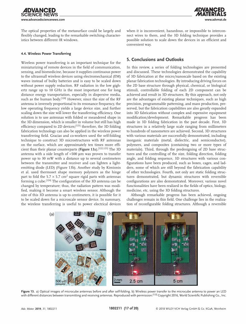
Wireless power transferring is an important technique for the miniaturizing of remote devices in the field of communication, sensing, and biomedicine, because it supplies continuous power to the ultrasmall wireless devices using electromechanical (EM) waves instead of bulky batteries and is easy to be scaled down without power supply reduction. RF radiation in the low gigh-ertz range up to 10 GHz is the most important one for long distance energy transportation, especially in dispersive media, such as the human body.[120] However, since the size of the RF antenna is inversely proportional to its resonance frequency, the low operating frequency yields a large device size, and further scaling down the size will lower the transferring efficiency. One solution is to use antennas with folded or meandered shape in the 3D dimension, which is smaller in volume but still has high efficiency compared to 2D devices;[121] therefore, the 3D folding fabrication technology can also be applied in the wireless power transferring field. Gracias and co-workers used the self-folding technique to construct 3D microstructures with RF antennas on the surface, which are approximately ten times more effi-cient than their planar counterparts (Figure 13a).[122,123] The 3D antenna with a side length of ≈500 µm was proven to transfer power up to 30 mW with a distance up to several centimeters between the transmitter and receiver and can lighten a light-emitting diode (LED) (Figure 13b). Another study by Kimionis et al. used thermoset shape memory polymers as the hinge part to fold the 5.7 × 5.7 cm2 square rigid parts with antennas forming a cube.[124] The configuration of the 3D antenna can be changed by temperature; thus, the radiation pattern was modi-fied, making it become a smart wireless sensor. Although the size of this 3D antenna is up to centimeters, it is possible for it to be scaled down for a microscale sensor device. In summary, the wireless transferring is useful to power electrical devices
when it is inconvenient, hazardous, or impossible to intercon-nect wires to them, and the 3D folding technique provides a possible solution to scale down the devices in an efficient and convenient way.
5. Conclusions and Outlooks
In this review, a series of folding technologies are presented and discussed. These technologies demonstrated the capability of 3D fabrication at the micro/nanoscale based on the existing planar fabrication technologies. By introducing driving forces on the 2D base structure through physical, chemical, or biological stimuli, controllable folding of each 2D component can be achieved and result in 3D structures. By this approach, not only are the advantages of existing planar techniques, such as high precision, programmable patterning, and mass production, pre-served, but the fabrication capabilities are also greatly expanded into 3D fabrication without complex and expensive equipment modification/development. Remarkable progress has been made in 3D folding fabrication in the past decade. First, 3D structures in a relatively large scale ranging from millimeters to hundreds of nanometers are achieved. Second, 3D structures with various materials are successfully demonstrated, including inorganic materials (metal, dielectric, and semiconductor), polymers, and composites (containing two or more types of materials). Third, through the predesigning of 2D base struc-tures and the controlling of the size, folding direction, folding angle, and folding sequence, 3D structures with various con-figurations have been produced, such as boxes, cages, and lad-ders, some of which are still beyond the fabrication capability of other technologies. Fourth, not only are static folding struc-tures demonstrated, but dynamic structures with reversible configurations are also demonstrated. Moreover, various novel functionalities have been realized in the fields of optics, biology, medicine, etc. using the 3D folding structures.
Although remarkable progress has been achieved, ongoing challenges remain in this field. One challenge lies in the realiza-tion of reconfigurable folding structures. Although a reversible
Figure 13. a) Optical images of microcube antennas before and after self-folding. b) Wireless power transfer to the microcube antenna to power an LED with different distances between transmitting and receiving antennas. Reproduced with permission.[122] Copyright 2016, World Scientific Publishing Co., Inc.
© 2018 WILEY-VCH Verlag GmbH & Co. KGaA, Weinheim1802211 (18 of 20)
www.advmat.dewww.advancedsciencenews.com
Adv. Mater. 2019, 31, 1802211
folding process can be realized through a magnetic field,[32] water drop syringing,[34] and strain gradient of Cu/Cr,[59] the reconfiguration is not flexible enough for fast and accurate manipulation. Another challenge involves the scaling down of the reconfigurable folding structures to the nanoscale, which has remarkable applications in active optical devices operating in the IR and visible ranges, and biomedical devices within blood vessels. Although nanoscale structures have been folded by the molten solder hinge[41] and focused ion beam[82] methods, they cannot be reversibly controlled. Therefore, the aim in the near future would be to develop an optimal folding technology with all the necessary features for specific applications. In addition to searching for new types of driving forces, a promising way would be the combination of different folding strategies within one structure. When these requirements are met, more extensive applications in physics, chemistry, and biology can be reached.
AcknowledgementsThe authors gratefully acknowledge the financial support from the National Key R&D Program of China (Grant Nos. 2016YFA0200800 and 2016YFA0200400), the National Natural Science Foundation of China (Grant Nos. 11674387, 11504414, 11704016, 61390503, 11574385, 11574368, and 11434017), the Key Research Program of Frontier Sciences of CAS (Grant No. QYZDJ-SSW-SLH042), the Beijing Municipal Natural Science Foundation (Grant No. 2172007), and the “Strategic Priority Research Program” of CAS (Grant No. XDB07020200).
Conflict of InterestThe authors declare no conflict of interest.
Keywords2D, 3D, folding, hinges, micro/nano-structures
Received: April 7, 2018Revised: June 24, 2018
Published online: October 1, 2018
[1] a) C.-M. Ho, Y.-C. Tai, Annu. Rev. Fluid Mech. 1998, 30, 579; b) H. Lorenz, M. Despont, N. Fahrni, J. Brugger, P. Vettiger, P. Renaud, Sens. Actuators, A 1998, 64, 33; c) M. Liao, Y. Koide, Crit. Rev. Solid State Mater. Sci. 2011, 36, 66; d) L. Midolo, A. Schliesser, A. Fiore, Nat. Nanotechnol. 2018, 13, 11.
[2] a) A. V. Kildishev, A. Boltasseva, V. M. Shalaev, Science 2013, 339, 1232009; b) C. Wang, C.-Z. Zhou, Z.-Y. Li, Opt. Express 2011, 19, 26948; c) Q. Bao, K. P. Loh, ACS Nano 2012, 6, 3677.
[3] a) Y. Du, E. Lo, S. Ali, A. Khademhosseini, Proc. Natl. Acad. Sci. USA 2008, 105, 9522; b) B. Zamanian, M. Masaeli, J. W. Nichol, M. Khabiry, M. J. Hancock, H. Bae, A. Khademhosseini, Small 2010, 6, 937; c) S. Zakharchenko, E. Sperling, L. Ionov, Biomac-romolecules 2011, 12, 2211; d) G. Ratheesh, J. R. Venugopal, A. Chinappan, H. Ezhilarasu, A. Sadiq, S. Ramakrishna, ACS Biomater. Sci. Eng. 2017, 3, 1175.
[4] a) C. E. S. Linder, M. Wegener, J. Zhou, T. Koschny, C. M. Soukoulis, Science 2004, 306, 1351; b) N. Katsarakis, T. Koschny, M. Kafesaki, E. N. Economou, C. M. Soukoulis, Appl. Phys. Lett. 2004, 84, 2943.
[5] J. K. Gansel, M. Thiel, M. S. Rill, M. Decker, K. Bade, V. Saile, G. von Freymann, S. Linden, M. Wegener, Science 2009, 325, 1513.
[6] a) M. Decker, M. Ruther, C. E. Kriegler, J. Zhou, C. M. Soukoulis, S. Linden, M. Wegener, Opt. Lett. 2009, 34, 2501; b) M. Decker, R. Zhao, C. M. Soukoulis, S. Linden, M. Wegener, Opt. Lett. 2010, 35, 1593.
[7] C. L. Randall, T. G. Leong, N. Bassik, D. H. Gracias, Adv. Drug Delivery Rev. 2007, 59, 1547.
[8] W. H. Ryu, M. Vyakarnam, R. S. Greco, F. B. Prinz, R. J. Fasching, Biomed. Microdevices 2007, 9, 845.
[9] M. Thiel, J. Fischer, G. von Freymann, M. Wegener, Appl. Phys. Lett. 2010, 97, 221102.
[10] T. Morita, R. Kometani, K. Watanabe, K. Kanda, Y. Haruyama, T. Hoshino, K. Kondo, T. Kaito, T. Ichihashi, J.-i. Fujita, M. Ishida, Y. Ochiai, T. Tajima, S. Matsui, J. Vac. Sci. Technol., B: Microelec-tron. Nanometer Struct.—Process., Meas., Phenom. 2003, 21, 2737.
[11] a) T. Ergin, N. Stenger, P. Brenner, J. B. Pendry, M. Wegener, Science 2010, 328, 337; b) T. Bückmann, M. Thiel, M. Kadic, R. Schittny, M. Wegener, Nat. Commun. 2014, 5, 4130; c) F. Klein, B. Richter, T. Striebel, C. M. Franz, G. von Freymann, M. Wegener, M. Bastmeyer, Adv. Mater. 2011, 23, 1341; d) E. J. Romans, E. J. Osley, L. Young, P. A. Warburton, W. Li, Appl. Phys. Lett. 2010, 97, 222506; e) A. Selimis, V. Mironov, M. Farsari, Microelec-tron. Eng. 2015, 132, 83; f) S. Juodkazis, V. Mizeikis, H. Misawa, J. Appl. Phys. 2009, 106, 051101.
[12] M. S. Rill, C. Plet, M. Thiel, I. Staude, G. von Freymann, S. Linden, M. Wegener, Nat. Mater. 2008, 7, 543.
[13] K. Fan, A. C. Strikwerda, H. Tao, X. Zhang, R. D. Averitt, Opt. Express 2011, 19, 12619.
[14] S. Zhang, W. J. Fan, B. K. Minhas, A. Frauenglass, K. J. Malloy, S. R. J. Brueck, Phys. Rev. Lett. 2005, 94, 037402.
[15] a) D. B. Burckel, J. R. Wendt, G. A. Ten Eyck, A. R. Ellis, I. Brener, M. B. Sinclair, Adv. Mater. 2010, 22, 3171; b) D. B. Burckel, J. R. Wendt, G. A. Ten Eyck, J. C. Ginn, A. R. Ellis, I. Brener, M. B. Sinclair, Adv. Mater. 2010, 22, 5053.
[16] A. P.-H. Edwin, J. H. Darren, J. M. Richard Jr., C. L. Dimitris, Smart Mater. Struct. 2014, 23, 094001.
[17] X. Fan, J. Y. Chung, Y. X. Lim, Z. Li, X. J. Loh, ACS Appl. Mater. Inter-faces 2016, 8, 33351.
[18] a) L. Ionov, Soft Matter 2011, 7, 6786; b) L. Ionov, Langmuir 2015, 31, 5015; c) V. B. Shenoy, D. H. Gracias, MRS Bull. 2012, 37, 847.
[19] L. Ionov, Macromol. Chem. Phys. 2013, 214, 1178.[20] M. Johnson, Y. Chen, S. Hovet, S. Xu, B. Wood, H. Ren, J. Tokuda,
Z. T. H. Tse, Int. J. Comput. Assist. Radio.l Surg. 2017, 12, 2023.[21] J. Rogers, Y. Huang, O. G. Schmidt, D. H. Gracias, MRS Bull.
2016, 41, 123.[22] a) Y. Liu, J. Genzer, M. D. Dickey, Prog. Polym. Sci. 2016, 52, 79;
b) T. G. Leong, A. M. Zarafshar, D. H. Gracias, Small 2010, 6, 792; c) Y. Zhang, F. Zhang, Z. Yan, Q. Ma, X. Li, Y. Huang, J. A. Rogers, Nat. Rev. Mater. 2017, 2, 17019.
[23] V. Pini, J. J. Ruz, P. M. Kosaka, O. Malvar, M. Calleja, J. Tamayo, Sci. Rep. 2016, 6, 29627.
[24] Z. Chen, R. Mohsen, Y. Gong, C. T. Chong, M. Hong, Adv. Mater. 2012, 24, OP143.
[25] J.-H. Na, A. A. Evans, J. Bae, M. C. Chiappelli, C. D. Santangelo, R. J. Lang, T. C. Hull, R. C. Hayward, Adv. Mater. 2015, 27, 79.
[26] L. Mahadevan, S. Rica, Science 2005, 307, 1740.[27] H. J. In, S. Kumar, Y. Shao-Horn, G. Barbastathis, Appl. Phys. Lett.
2006, 88, 083104.[28] J. W. C. Dunlop, R. Weinkamer, P. Fratzl, Mater. Today 2011, 14, 70.[29] a) R. Kaplan, J. Klobušický, S. Pandey, D. H. Gracias, G. Menon,
Artif. Life 2014, 20, 409; b) S. Pandey, D. Johnson, R. Kaplan, J. Klobusicky, G. Menon, D. H. Gracias, PLoS One 2014, 9, e108960.
[30] a) J. W. Judy, R. S. Muller, J. Microelectromech. Syst. 1997, 6, 249; b) Y. W. Yi, C. Liu, J. Microelectromech. Syst. 1999, 8, 10.

© 2018 WILEY-VCH Verlag GmbH & Co. KGaA, Weinheim1802211 (19 of 20)
www.advmat.dewww.advancedsciencenews.com
Adv. Mater. 2019, 31, 1802211
[31] Y. W. Yi, C. Liu, Sens. Actuators, A 1999, 78, 205.[32] E. Iwase, I. Shimoyama, J. Microelectromech. Syst. 2005, 14, 1265.[33] H. J. In, H. Lee, A. J. Nichol, S.-G. Kim, G. Barbastathis,
J. Vac. Sci. Technol., B: Microelectron. Nanometer Struct.—Process., Meas., Phenom. 2008, 26, 2509.
[34] A. Legrain, T. G. Janson, J. W. Berenschot, L. Abelmann, N. R. Tas, J. Appl. Phys. 2014, 115, 214905.
[35] a) C. Py, P. Reverdy, L. Doppler, J. Bico, B. Roman, C. N. Baroud, Eur. Phys. J.: Spec. Top. 2009, 166, 67; b) C. Py, P. Reverdy, L. Doppler, J. Bico, B. Roman, C. N. Baroud, Phys. Rev. Lett. 2007, 98, 156103.
[36] Z. Yan, F. Zhang, J. Wang, F. Liu, X. Guo, K. Nan, Q. Lin, M. Gao, D. Xiao, Y. Shi, Y. Qiu, H. Luan, J. H. Kim, Y. Wang, H. Luo, M. Han, Y. Huang, Y. Zhang, J. A. Rogers, Adv. Funct. Mater. 2016, 26, 2629.
[37] J. L. Tan, J. Tien, D. M. Pirone, D. S. Gray, K. Bhadriraju, C. S. Chen, Proc. Natl. Acad. Sci. USA 2003, 100, 1484.
[38] K. Kuribayashi-Shigetomi, H. Onoe, S. Takeuchi, PLoS One 2012, 7, e51085.
[39] R. R. A. Syms, E. M. Yeatman, V. M. Bright, G. M. Whitesides, J. Microelectromech. Syst. 2003, 12, 387.
[40] a) J.-H. Cho, D. H. Gracias, Nano Lett. 2009, 9, 4049; b) H. R. Kwag, J.-H. Cho, S.-Y. Park, J. Park, D. H. Gracias, Faraday Discuss. 2016, 191, 61.
[41] J.-H. Cho, M. D. Keung, N. Verellen, L. Lagae, V. V. Moshchalkov, P. Van Dorpe, D. H. Gracias, Small 2011, 7, 1943.
[42] D. H. Gracias, V. Kavthekar, J. C. Love, K. E. Paul, G. M. Whitesides, Adv. Mater. 2002, 14, 235.
[43] B. Gimi, T. Leong, Z. Gu, M. Yang, D. Artemov, Z. M. Bhujwalla, D. H. Gracias, Biomed. Microdevices 2005, 7, 341.
[44] T. Leong, Z. Gu, T. Koh, D. H. Gracias, J. Am. Chem. Soc. 2006, 128, 11336.
[45] S. Pandey, M. Ewing, A. Kunas, N. Nguyen, D. H. Gracias, G. Menon, Proc. Natl. Acad. Sci. USA 2011, 108, 19885.
[46] a) J. Wang, M. Patel, D. H. Gracias, Nano 2009, 4, 1; b) A. Azam, T. G. Leong, A. M. Zarafshar, D. H. Gracias, PLoS One 2009, 4, e4451.
[47] J.-H. Cho, A. Azam, D. H. Gracias, Langmuir 2010, 26, 16534.[48] M. Rao, J. C. Lusth, S. L. Burkett, J. Vac. Sci. Technol., B: Nano-
technol. Microelectron.: Mater., Process., Meas., Phenom. 2013, 31, 032002.
[49] a) Y. K. Hong, R. R. A. Syms, K. S. J. Pister, L. X. Zhou, J. Micro-mech. Microeng. 2005, 15, 663; b) R. R. A. Syms, IEEE Photonics Technol. Lett. 2000, 12, 1519.
[50] A. Azam, K. E. Laflin, M. Jamal, R. Fernandes, D. H. Gracias, Biomed. Microdevices 2011, 13, 51.
[51] K. Suzuki, H. Yamada, H. Miura, H. Takanobu, Microsyst. Technol. 2007, 13, 1047.
[52] P. O. Vaccaro, K. Kubota, T. Aida, Appl. Phys. Lett. 2001, 78, 2852.[53] J. M. Z. Ocampo, P. O. Vaccaro, T. Fleischmann, T.-S. Wang,
K. Kubota, T. Aida, T. Ohnishi, A. Sugimura, R. Izumoto, M. Hosoda, S. Nashima, Appl. Phys. Lett. 2003, 83, 3647.
[54] P. O. Vaccaro, K. Kubota, T. Fleischmann, S. Saravanan, T. Aida, Microelectron. J. 2003, 34, 447.
[55] C. Li, Y.-J Lai, C.-Y. Wu, J. A. Yeh, R.-S. Huang, J. Micro-mech. Microeng. 2005, 15, 55.
[56] A. Vorob’ev, P. Vaccaro, K. Kubota, S. Saravanan, T. Aida, Jpn. J. Appl. Phys. 2003, 42, 4024.
[57] a) R. W. Hoffman, R. D. Daniels, E. C. Crittenden, Proc. Phys. Soc., London 1954, 67, 497; b) P. Tyagi, N. Bassik, T. G. Leong, J. H. Cho, B. R. Benson, D. H. Gracias, J. Microelectromech. Syst. 2009, 18, 784; c) D. Joung, K. Agarwal, H.-R. Park, C. Liu, S.-H. Oh, J.-H. Cho, Adv. Electron. Mater. 2016, 2, 1500459.
[58] N. Bassik, G. M. Stern, D. H. Gracias, Appl. Phys. Lett. 2009, 95, 091901.
[59] J. S. Randhawa, M. D. Keung, P. Tyagi, D. H. Gracias, Adv. Mater. 2010, 22, 407.
[60] T. G. Leong, B. R. Benson, E. K. Call, D. H. Gracias, Small 2008, 4, 1605.
[61] T. G. Leong, C. L. Randall, B. R. Benson, A. M. Zarafshar, D. H. Gracias, Lab Chip 2008, 8, 1621.
[62] T. G. Leong, C. L. Randall, B. R. Benson, N. Bassik, G. M. Stern, D. H. Gracias, Proc. Natl. Acad. Sci. USA 2009, 106, 703.
[63] J. S. Randhawa, T. G. Leong, N. Bassik, B. R. Benson, M. T. Jochmans, D. H. Gracias, J. Am. Chem. Soc. 2008, 130, 17238.
[64] K. E. Laflin, C. J. Morris, T. Muqeem, D. H. Gracias, Appl. Phys. Lett. 2012, 101, 131901.
[65] Y. ChangKyu, X. Rui, P. JaeHyun, C. Jaepyeong, D. N. Thao, H. G. David, Smart Mater. Struct. 2014, 23, 094008.
[66] a) S. Fusco, M. S. Sakar, S. Kennedy, C. Peters, R. Bottani, F. Starsich, A. Mao, G. A. Sotiriou, S. Pané, S. E. Pratsinis, D. Mooney, B. J. Nelson, Adv. Mater. 2014, 26, 952; b) N. Bassik, B. T. Abebe, K. E. Laflin, D. H. Gracias, Polymer 2010, 51, 6093.
[67] C. M. Andres, J. Zhu, T. Shyu, C. Flynn, N. A. Kotov, Langmuir 2014, 30, 5378.
[68] a) J. Zhou, S. A. Turner, S. M. Brosnan, Q. Li, J.-M. Y. Carrillo, D. Nykypanchuk, O. Gang, V. S. Ashby, A. V. Dobrynin, S. S. Sheiko, Macromolecules 2014, 47, 1768; b) S. M. Felton, K. P. Becker, D. M. Aukes, R. J. Wood, J. Micromech. Microeng. 2015, 25, 085004; c) T. S. Shim, S.-H. Kim, C.-J. Heo, H. C. Jeon, S.-M. Yang, Angew. Chem., Int. Ed. 2012, 51, 1420; d) X. Li, M. J. Serpe, Adv. Funct. Mater. 2014, 24, 4119; e) M. Behl, M. Y. Razzaq, A. Lendlein, Adv. Mater. 2010, 22, 3388; f) M. J. Harrington, K. Razghandi, F. Ditsch, L. Guiducci, M. Rueggeberg, J. W. C. Dunlop, P. Fratzl, C. Neinhuis, I. Burgert, Nat. Commun. 2011, 2, 337.
[69] a) Y. Liu, R. Mailen, Y. Zhu, M. D. Dickey, J. Genzer, Phys. Rev. E 2014, 89, 042601; b) Y. Liu, J. K. Boyles, J. Genzer, M. D. Dickey, Soft Matter 2012, 8, 1764.
[70] Y. Liu, M. Miskiewicz, M. J. Escuti, J. Genzer, M. D. Dickey, J. Appl. Phys. 2014, 115, 204911.
[71] J. Ryu, M. D’Amato, X. Cui, K. N. Long, H. J. Qi, M. L. Dunn, Appl. Phys. Lett. 2012, 100, 161908.
[72] Y.-W. Lu, C.-J. Kim, Appl. Phys. Lett. 2006, 89, 164101.[73] S. Konishi, F. Kawai, P. Cusin, Sens. Actuators, A 2001, 89, 28.[74] W. J. Arora, S. Sijbrandij, L. Stern, J. Notte, H. I. Smith,
G. Barbastathis, J. Vac. Sci. Technol., B: Microelectron. Nanometer Struct.—Process., Meas., Phenom. 2007, 25, 2184.
[75] P. F. P. Fichtner, J. R. Kaschny, R. A. Yankov, A. Mücklich, U. Kreißig, W. Skorupa, Appl. Phys. Lett. 1997, 70, 732.
[76] W. J. Arora, H. I. Smith, G. Barbastathis, Microelectron. Eng. 2007, 84, 1454.
[77] S. R. Nitul, B. Amit, H. C. Verma, Nanotechnology 2011, 22, 485302.
[78] C. Borschel, S. Spindler, D. Lerose, A. Bochmann, S. H. Christiansen, S. Nietzsche, M. Oertel, C. Ronning, Nanotech-nology 2011, 22, 185307.
[79] K. Das, J. B. Freund, H. T. Johnson, Nanotechnology 2014, 25, 035303.
[80] C.-L. Wu, F.-C. Li, C.-W. Pao, D. J. Srolovitz, Nano Lett. 2017, 17, 249.
[81] a) A. Cui, W. Li, Q. Luo, Z. Liu, C. Gu, Appl. Phys. Lett. 2012, 100, 143106; b) A. Cui, W. Li, Q. Luo, Z. Liu, C. Gu, Microelectron. Eng. 2012, 98, 409; c) A. Cui, J. C. Fenton, W. Li, T. H. Shen, Z. Liu, Q. Luo, C. Gu, Appl. Phys. Lett. 2013, 102, 213112.
[82] A. Cui, Z. Liu, J. Li, T. H. Shen, X. Xia, Z. Li, Z. Gong, H. Li, B. Wang, J. Li, H. Yang, W. Li, C. Gu, Light: Sci. Appl. 2015, 4, e308.
[83] Z. Liu, A. Cui, Z. Gong, H. Li, X. Xia, T. H. Shen, J. Li, H. Yang, W. Li, C. Gu, Sci. Rep. 2016, 6, 28764.
© 2018 WILEY-VCH Verlag GmbH & Co. KGaA, Weinheim1802211 (20 of 20)
www.advmat.dewww.advancedsciencenews.com
Adv. Mater. 2019, 31, 1802211
[84] S. Yang, Z. Liu, L. Jin, W. Li, S. Zhang, J. Li, C. Gu, ACS Photonics 2017, 4, 2650.
[85] Z. Liu, J. Li, Z. Liu, W. Li, J. Li, C. Gu, Z.-Y. Li, Sci. Rep. 2017, 7, 8010.
[86] Z. Liu, S. Du, A. Cui, Z. Li, Y. Fan, S. Chen, W. Li, J. Li, C. Gu, Adv. Mater. 2017, 29, 1606298.
[87] Y. Mao, Y. Pan, W. Zhang, R. Zhu, J. Xu, W. Wu, Nano Lett. 2016, 16, 7025.
[88] a) X. Guo, H. Li, B. Yeop Ahn, E. B. Duoss, K. J. Hsia, J. A. Lewis, R. G. Nuzzo, Proc. Natl. Acad. Sci. USA 2009, 106, 20149; b) J. W. van Honschoten, J. W. Berenschot, T. Ondarçuhu, R. G. P. Sanders, J. Sundaram, M. Elwenspoek, N. R. Tas, Appl. Phys. Lett. 2010, 97, 014103; c) A. Legrain, E. J. W. Berenschot, N. R. Tas, L. Abelmann, PLoS One 2015, 10, e0125891; d) A. Legrain, J. W. Berenschot, N. R. Tas, L. Abelmann, Microelectron. Eng. 2015, 140, 60; e) B. Roman, J. Bico, J. Phys.: Condens. Matter 2010, 22, 493101; f) N. D. Brubaker, J. Lega, Phys. Lett. A 2016, 380, 83.
[89] I. White, M. J. Sully, Water Resour. Res. 1987, 23, 1514.[90] G. W. Dahlmann, E. M. Yeatman, Electron. Lett. 2000, 36,
1707.[91] R. R. A. Syms, J. Microelectromech. Syst. 1999, 8, 448.[92] C. C. Chen, C. T. Hsiao, S. Sun, K.-Y. Yang, P. C. Wu, W. T. Chen,
Y. H. Tang, Y.-F. Chau, E. Plum, G.-Y. Guo, N. I. Zheludev, D. P. Tsai, Opt. Express 2012, 20, 9415.
[93] O. G. Schmidt, K. Eberl, Nature 2001, 410, 168.[94] K. Ju-Nan, L. Gwo-Bin, P. Wen-Fung, L. Huei-Huang,
Jpn. J. Appl. Phys. 2005, 44, 3180.[95] E. Moiseeva, Y. M. Senousy, S. McNamara, C. K. Harnett, J. Micro-
mech. Microeng. 2007, 17, N63.[96] C. H. Hsueh, Thin Solid Films 2002, 418, 182.[97] T. Xie, Nature 2010, 464, 267.[98] C. Liu, H. Qin, P. T. Mather, J. Mater. Chem. 2007, 17, 1543.[99] a) A. Lendlein, H. Jiang, O. Junger, R. Langer, Nature 2005, 434,
879; b) H. Koerner, G. Price, N. A. Pearce, M. Alexander, R. A. Vaia, Nat. Mater. 2004, 3, 115.
[100] W. M. Huang, B. Yang, L. An, C. Li, Y. S. Chan, Appl. Phys. Lett. 2005, 86, 114105.
[101] R. Mohr, K. Kratz, T. Weigel, M. Lucka-Gabor, M. Moneke, A. Lendlein, Proc. Natl. Acad. Sci. USA 2006, 103, 3540.
[102] a) S. Xu, Z. Yan, K.-I. Jang, W. Huang, H. Fu, J. Kim, Z. Wei, M. Flavin, J. McCracken, R. Wang, A. Badea, Y. Liu, D. Xiao, G. Zhou, J. Lee, H. U. Chung, H. Cheng, W. Ren, A. Banks, X. Li, U. Paik, R. G. Nuzzo, Y. Huang, Y. Zhang, J. A. Rogers, Sci-ence 2015, 347, 154; b) Y. Zhang, Z. Yan, K. Nan, D. Xiao, Y. Liu, H. Luan, H. Fu, X. Wang, Q. Yang, J. Wang, W. Ren, H. Si, F. Liu, L. Yang, H. Li, J. Wang, X. Guo, H. Luo, L. Wang, Y. Huang, J. A. Rogers, Proc. Natl. Acad. Sci. USA 2015, 112, 11757.
[103] a) A. K. Geim, K. S. Novoselov, Nat. Mater. 2007, 6, 183; b) N. N. Klimov, S. Jung, S. Zhu, T. Li, C. A. Wright, S. D. Solares,
D. B. Newell, N. B. Zhitenev, J. A. Stroscio, Science 2012, 336, 1557; c) C. Lee, X. Wei, J. W. Kysar, J. Hone, Science 2008, 321, 385; d) M. Liu, X. Yin, E. Ulin-Avila, B. Geng, T. Zentgraf, L. Ju, F. Wang, X. Zhang, Nature 2011, 474, 64.
[104] E. Prada, P. San-Jose, L. Brey, Phys. Rev. Lett. 2010, 105, 106802.[105] D. Rainis, F. Taddei, M. Polini, G. León, F. Guinea, V. I. Fal’ko,
Phys. Rev. B 2011, 83, 165403.[106] D. Joung, A. Nemilentsau, K. Agarwal, C. Dai, C. Liu, Q. Su, J. Li,
T. Low, S. J. Koester, J.-H. Cho, Nano Lett. 2017, 17, 1987.[107] W. Xu, Z. Qin, C.-T. Chen, H. R. Kwag, Q. Ma, A. Sarkar,
M. J. Buehler, D. H. Gracias, Sci. Adv. 2017, 3, e1701084.[108] H. Zhang, J. K. Jackson, M. Chiao, Adv. Funct. Mater. 2017, 27,
1703606.[109] A. S. Hoffman, J. Controlled Release 2008, 132, 153.[110] R. Fernandes, D. H. Gracias, Adv. Drug Delivery Rev. 2012, 64,
1579.[111] H. Ye, C. L. Randall, T. G. Leong, D. A. Slanac, E. K. Call,
D. H. Gracias, Angew. Chem. 2007, 119, 5079.[112] J. R. Park, D. A. Slanac, T. G. Leong, H. Ye, D. B. Nelson,
D. H. Gracias, J. Microelectromech. Syst. 2008, 17, 265.[113] K. Malachowski, J. Breger, H. R. Kwag, M. O. Wang, J. P. Fisher,
F. M. Selaru, D. H. Gracias, Angew. Chem., Int. Ed. 2014, 53, 8045.[114] a) C. L. Randall, E. Gultepe, D. H. Gracias, Trends Biotechnol. 2012,
30, 138; b) K. Malachowski, M. Jamal, Q. Jin, B. Polat, C. J. Morris, D. H. Gracias, Nano Lett. 2014, 14, 4164.
[115] F. Lim, A. Sun, Science 1980, 210, 908.[116] a) C. L. Randall, A. Gillespie, S. Singh, T. G. Leong, D. H. Gracias,
Anal. Bioanal. Chem. 2009, 393, 1217; b) C. L. Randall, Y. V. Kalinin, M. Jamal, T. Manohar, D. H. Gracias, Lab Chip 2011, 11, 127.
[117] G. Stoychev, N. Puretskiy, L. Ionov, Soft Matter 2011, 7, 3277.[118] J. C. Breger, C. Yoon, R. Xiao, H. R. Kwag, M. O. Wang, J. P. Fisher,
T. D. Nguyen, D. H. Gracias, ACS Appl. Mater. Interfaces 2015, 7, 3398.
[119] Z. Liu, Z. Liu, J. Li, W. Li, J. Li, C. Gu, Z.-Y. Li, Sci. Rep. 2016, 6, 27817.
[120] A. S. Y. Poon, S. O. Driscoll, T. H. Meng, IEEE Trans. Antennas Propag. 2010, 58, 1739.
[121] a) J. J. Adams, E. B. Duoss, T. F. Malkowski, M. J. Motala, B. Y. Ahn, R. G. Nuzzo, J. T. Bernhard, J. A. Lewis, Adv. Mater. 2011, 23, 1335; b) S. R. Best, IEEE Antennas Propag. Mag. 2004, 46, 9; c) T. J. Warnagiris, T. J. Minardo, IEEE Trans. Antennas Propag. 1998, 46, 1797.
[122] P. Anacleto, E. Gultepe, S. Gomes, P. M. Mendes, D. H. Gracias, Technol. Innovation 2016, 4, 120.
[123] S. Gomes, J. Fernandes, P. Anacleto, P. M. Mendes, E. Gultepe, D. Gracias, presented at 2014 44th European Microwave Conf., Rome, Italy, October 2014.
[124] J. Kimionis, M. Isakov, B. S. Koh, A. Georgiadis, M. M. Tentzeris, IEEE Trans. Microwave Theor. Tech 2015, 63, 4521.


![Self-Folding and Self-Actuating Robots: A Pneumatic Approach · pneumatic pouch motors to actuate folding [18]. Unlike other pneumatic actuators, pouch motors are made with a 2D fabrication](https://img.pdfslide.net/doc/110x75/5e894a6137bc69003e0a2b24/self-folding-and-self-actuating-robots-a-pneumatic-approach-pneumatic-pouch-motors.jpg)