Embed Size (px)
Citation preview
Formation and Growth of Tin Whiskers on AluminumTin Alloys*
Koji Murakami1, Makoto Hino1, Yutaka Mitooka1 and Teruto Kanadani2
1Industrial Technology Research Institute of Okayama Prefectural Government, Okayama 701-1296, Japan2Faculty of Engineering, Okayama University of Science, Okayama 700-0005, Japan
In order to clarify the mechanism of formation of nodules and whiskers on the conducting wires used in aluminum electrolytic capacitors,aluminumtin binary alloys were subjected to an investigation as the model alloys for the joints in the conducting wires. The concentration of tinin the binary alloys was 1, 5 or 10 at%. The 10 at% tin alloy showed the highest number of nodules or whiskers on its polished surface afterstoring under ambient conditions for 7.8Ms. Many whiskers whose length were greater than several tens of micrometers were observed for 5 at%tin alloy. The 1 at% tin alloy showed few nodules or whiskers. Growth of the nodules and whiskers is caused by diffusion of the tin atoms fromthe strained or high-energy areas into the low-energy ones or the root grains. The extrusion toward the surface at the root grains then developsnodules and whiskers. As a preventive measure of whisker formation, selective etching of the aluminum phase using a solution of sodiumhydroxide was confirmed to be successful. Thus the aluminum phase was thought to form a non-uniform distribution of strain in the tin phase.This acts as the driving force for diffusion of the tin atoms. [doi:10.2320/matertrans.L-M2011830]
(Received June 9, 2011; Accepted October 6, 2011; Published November 30, 2011)
Keywords: aluminumtin alloy, tin whisker, diffusion, vacancy, crystal orientation
1. Introduction
Aluminum electrolytic capacitors are used in the powersupplies for electric and electronic equipment, whoseconducting wires are manufactured by joining aluminumtabs, attached to the anode/cathode foils of aluminum, withsteel wires coated with electroplated films of copper and tin.1)
The films of tin on the copper-coated steel wires areelectroplated for soldering to circuit boards, and the jointsin the conducting wires consist of an aluminumtinironcopper alloy which assure the joining strength required inpackaging and subsequent practical use. Short circuits causedby the formation of tin whiskers on the joints have recentlybecome a serious problem in accordance with the RoHS(Restriction of Hazardous Substances) directive whichrequires a lead-free process.27) In this article, the word‘lead’ means the element (Pb) hereafter, and the word ‘lead’which means conducting wire is not used to avoid confusion.The whiskers, whose length can be more than severalhundred micrometers, consist of straight, curved and kinkedparts. They develop from the tin phase in the joints formed byfusion and solidification of the electroplated films of tin onthe conducting wires during the joining process.
Regarding the electroplated films of tin and tin-basedalloys for connectors in electronic equipment, short circuitswere once solved by the electroplating of a tin-lead alloyinstead of tin after a number of accidents in the telephoneexchangers in the 1940s.8) However, other measures forsuppressing whiskers are required which satisfies the above-mentioned trend of lead-free products. While heat treatment,controlling grain size and multilayering have successfullybeen attempted,913) the detailed mechanism of the formationof whiskers and the role of alloying elements in the platedfilms, which suppress the whiskers, remain unknown. In thesystem of an electroplated film of tin on a substrate of copperunder ambient conditions without external stress, theformation of a coppertin intermetallic compound (Cu6Sn5),
an increase in the internal stress and the fracture of the oxidefilm are commonly considered to be the major factorsaffecting the development of whiskers.9,1421) The formationof Cu6Sn5, which accompanies an increase in volume, ismentioned to cause compressive deformation of the tin whichcontacts the grains of Cu6Sn5, then whiskers grow withfracture of the oxide film on the tin and subsequent expansionat the root.9)
On the other hand, few cases of the whiskers on the jointsin conducting wires have been reported compared to those onthe electroplated films of tin, and the relation between thedevelopment of whiskers and the microstructure of jointsremains unknown. Since the microstructure of joints iscomplicated and the formation of residual stress significantlydepends on the heating-cooling process during joining, it isvery difficult to understand and predict the behavior ofwhiskers. However, the joints mainly consist of aluminumand tin, whose binary system is considered to be a significantmodel for understanding the nature of whiskers generated bythe alloying of tin, which bears no whiskers under ambientconditions, with aluminum. In this article, the binary alloysof aluminumtin are used as model alloys for the joints, andthe morphologies of the whiskers on the alloys and theircrystallographic properties are reported.
2. Experimental
The aluminumtin alloys were prepared by die casting,whose starting materials were 99.999mass% aluminum and99.9mass% tin. The concentration of tin was 1, 5 or 10 at%,and the shape of the alloys was a cylinder whose diameterand length were 15.5mm and 90mm, respectively. Hereafter,the alloys are expressed as ‘1 Sn alloy’, ‘5 Sn alloy’ or ‘10 Snalloy’ for simplicity.
The alloys were quenched in water after casting, then2mm-thick discs were cut out of the cast alloys, and theirpolished surfaces were subjected to the following evalua-tions. The rough grinding was conducted using siliconcarbide waterproof abrasive papers of #1000#4000 grade,then the ground surfaces were finished by polishing with a
+This Paper was Originally Published in Japanese in J. JILM 61 (2011)142148.
Materials Transactions, Vol. 53, No. 1 (2012) pp. 209 to 216©2011 The Japan Institute of Light Metals
colloidal silica suspension in order to obtain a mirror surfaceon which electron backscatter diffraction (EBSD) measure-ments were possible. Some of the specimens underwent heattreatment after cutting, and its effect on the development ofwhiskers on the mirror-polished surfaces was examined.
An infrared lamp heater with a cylindrical quartz chamberwas used for the heat treatment. The chamber, in which thespecimens were placed, was evacuated up to 1.3 © 10¹3 Pa.Immediately after the evacuation was stopped, argon gas wasintroduced into the chamber up to 1.0 © 105 Pa, then thespecimens underwent the heat treatment. The specimens wereheated to 473K at the rate of 0.1K/s. After maintaining thetemperature for 43.2 ks, the specimens were cooled to roomtemperature at the rate of ¹5.6 © 10¹3K/s. The surface ofthe as-cast 5 Sn alloy, immersed in a solution of 1 kmol/m3
sodium hydroxide (298K18 ks), was used for the evalua-tions in order to examine the effect of chemical treatment onthe whisker development. The treatment is later expressed as‘sodium hydroxide immersion’.
The development of whiskers under ambient conditions onthe polished surfaces or on the surface which had undergonethe sodium hydroxide immersion was observed at fixedpoints. The fixed-point observation was carried out severaltimes for elapsed times up to 7.8Ms after polishing.Hereafter, “fixed-point observation” will be expressed as‘FPO’ for simplicity. A field emission electron probemicroanalysis (FE-EPMA) was used for the FPO, in whichthe acceleration voltage and the probe current were 15 kVand5 nA, respectively. The images were collected either by thesecondary electron (SE) mode or back-scattered electron (BE,compositional mode) one, and the images are later expressedas ‘SEI’ or ‘BEI’, respectively. The marks for the FPO werethe indentations made by the micro Vickers hardness testerwith the indenting force of 980mN. The indentations were atthe center of the evaluation planes, around which the FPOwas conducted. Scanning white light interferometry22) wasused for measuring the three-dimensional topology of theevaluation plane after the sodium hydroxide immersion.
The residual stress was measured by X-ray diffraction onthe surfaces of the 5 Sn and 10 Sn alloys immediately afterthe polishing or the sodium hydroxide immersion. A four-axis microfocus X-ray diffractometer with an xyz-micro-positioner on the º-axis was used for the measurement. TheX-ray source was a rotating anode of copper, and the X-raytaken from the point source was monochromated by thegraphite (0002) plane (wavelength CuK¡ = 0.1542 nm). TheX-ray flux was finally shaped by a collimator whose diameterwas 300 µm, then irradiated on the surface of the evaluationplanes. A two-dimensional detector was used for themeasurement of the scattered X-rays, and the specimenswere oscillated in the xy-plane (¦x, ¦y = 0.5mm) todecrease the deficiencies in the Debye rings. The intensityprofiles of the diffraction peak of (620)Sn(2ª = 113.34°) wereobtained for a number of configurations of the specimen, thatis, the axes of º and » were changed to trace the shifts of thediffraction peak positions in the three-dimensional reciprocalspace. Each peak position was the center of the Gaussianfitted to the 2ª-intensity data by the least square method. Thepeak shift data were then converted to strain by a least squarecalculation.23) Although the Young’s modulus of tin depends
on the crystal orientation, the value was assumed to beconstant (E = 41.4GPa), and the Poisson’s ratio was set to¯ = 0.3 to obtain the stress from the strain. The error is³5MPa, estimated by the diffraction peak position and theprecision in the determination of the peak position. The X-raypenetration depth was ³20 and ³15 µm for the 5 Sn and10 Sn alloys, respectively. Each value corresponds to thethickness of the specimen which gives 80% of the intensityobtained from the specimen of infinite thickness.
The relation between the growth of the whiskers and theircrystallographic properties was investigated on the surfacesand cross sections of the whiskers by EBSD mounted in theFE-EPMA. The acceleration voltage and the probe currentof the primary electron beam were 20 kV and 10 nA,respectively, and the primary electron beam was scannedat intervals of 50100 nm. Cross sections for the EBSDmeasurement were prepared by microtoming with knives ofcemented carbide or diamond whose edge angle was 45°. Theformer was used for the rough shaping, and the latter was forthe final cut in which the clearance angle, the feed and thecutting speed were 6°, 50 nm and 0.1mm/s, respectively.
3. Experimental Results
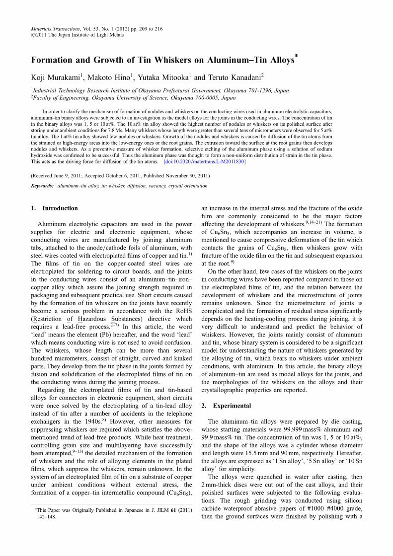
3.1 Microstructure of aluminumtin alloyFigure 1 shows the microstructure of the as-cast 5 Sn alloy
obtained by EBSD. Based on Fig. 1(a), the 5 Sn alloyconsists of two phases of aluminum and tin. The grains ofaluminum are surrounded by the tin phase whose thickness isseveral micrometers. Many low-angle grain boundaries existin the aluminum and tin at which the rotation angles aroundthe common rotation axes are less than 15° [Fig. 1(b)].
3.2 Fixed-point observationFigures 2, 3 and 4 are the FPOs (SEIs) which show the
time-dependent changes on the polished surfaces of the as-cast 1 Sn, 5 Sn and 10 Sn alloys. The microstructures of the1 Sn and 10 Sn alloys are similar to that of the 5 Sn alloy(Fig. 1), and a number of cavities exist in the tin phase ofthe 10 Sn alloy (Fig. 4). Although the alloys are prepared bydie casting, aluminum does not exhibit a marked dendriticstructure in the evaluation areas. As the time passed afterpolishing, nodules were formed on certain points of the tin inall the alloys, part of which developed into whiskers. Thecircles in Figs. 2, 3 and 4 indicate the locations of the nodulesor the whiskers. While all the nodules or whiskers in the fieldof view (FOV) of the 1 Sn alloy are indicated by the circles(Fig. 2), those in the upper-left quarter of the FOVare circledfor the 5 Sn alloy (Fig. 3) and 10 Sn alloy (Fig. 4). Thefrequency of occurrence of nodules or whiskers on the 1 Snalloy was 11mm¹2 at 0.52Ms, then increased to 15mm¹2 at7.8Ms. For the 5 Sn and 10 Sn alloys, the frequencies in theupper-left quarters were 3.7 © 102mm¹2 and 6.6 © 102mm¹2
at 0.52Ms, then increased to 6.3 © 102mm¹2 and 8.1 ©102mm¹2 at 7.8Ms, respectively. No remarkable relation wasconfirmed between the location of the nodules or whiskersand the morphology of the tin and aluminum. Manywhiskers, which developed up to several tens of micrometersor 100 µm in length, are observed on the 5 Sn alloy [7.8Ms,Fig. 3(c)] compared to the 10 Sn alloy [Fig. 4(c)].
K. Murakami, M. Hino, Y. Mitooka and T. Kanadani210

(a)
100 µm
(b)
Nodule
100 µm
(c)
100 µm
Fig. 2 Fixed-point observation of as-cast 1 Sn alloy (SEI, circles indicate whiskers or nodules, (a) As polished, (b) Kept under ambientconditions for 0.52Ms after polishing, (c) 7.8Ms).
100 5 µm
(a)
Al
Al
Al
Al
Al
Al
AlAl
001
110
5 µm
(b)
> 15 deg.
Rotation angle < 15 deg.
Fig. 1 Microstructure of as-cast 5 Sn alloy obtained by EBSD (Step size 100 nm, (a) ND-inverse pole figure map of tin; black areascorrespond to aluminum, (b) Grain boundary map).
(a)
100 µm
(b)
Nodule
100 µm
(c)
Whisker
100 µm
Fig. 3 Fixed-point observation of as-cast 5 Sn alloy (SEI, circles indicate whiskers or nodules, (a) As polished, (b) Kept under ambientconditions for 0.52Ms after polishing, (c) 7.8Ms).
(a)
Cavity
100 µm
(b)
Nodule
100 µm
(c)
100 µm
Fig. 4 Fixed-point observation of as-cast 10 Sn alloy (SEI, circles indicate whiskers or nodules, (a) As polished, (b) Kept under ambientconditions for 0.52Ms after polishing, (c) 7.8Ms).
Formation and Growth of Tin Whiskers on AluminumTin Alloys 211
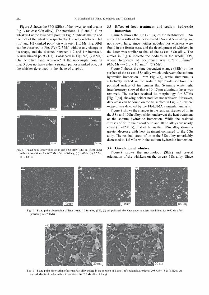
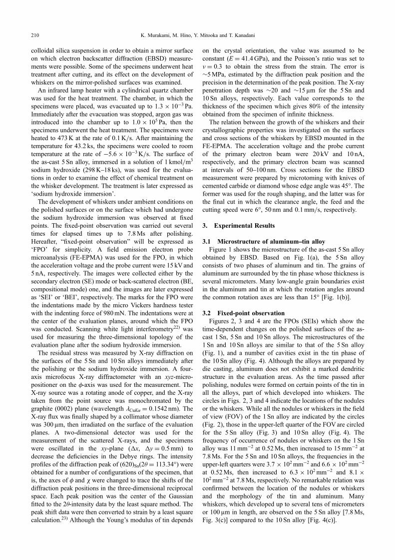
Figure 5 shows the FPO (SEIs) of the lower-central area inFig. 3 (as-cast 5 Sn alloy). The notations ‘1-1’ and ‘1-r’ onwhisker-1 at the lower-left point in Fig. 5 indicate the tip andthe root of the whisker, respectively. The region between 1-1(tip) and 1-2 (kinked point) on whisker-1 [1.0Ms, Fig. 5(b)]can be observed in Fig. 5(c) (2.7Ms) without any change inits shape, and the distance between 1-2 and 1-r increased.A new kinked point (1-3) is observed in Fig. 5(d) (7.8Ms).On the other hand, whisker-2 at the upper-right point inFig. 5 does not have either a straight part or a kinked one, butthe whisker developed in the shape of a spiral.
3.3 Effect of heat treatment and sodium hydroxideimmersion
Figure 6 shows the FPO (SEIs) of the heat-treated 10 Snalloy. The results of the heat-treated 1 Sn and 5 Sn alloys arenot shown here, since neither nodules nor whiskers werefound in the former case, and the development of whiskers inthe latter was similar to that of the as-cast 5 Sn alloy. Thecircles in Fig. 6 indicate the nodules in the whole FOV,whose frequency of occurrence was 0.71 © 102mm¹2
(0.60Ms) ¼ 2.0 © 102mm¹2 (7.8Ms).Figure 7 shows the time-dependent change (BEIs) on the
surface of the as-cast 5 Sn alloy which underwent the sodiumhydroxide immersion. From Fig. 7(a), while aluminum isselectively etched in the sodium hydroxide solution, thepolished surface of tin remains flat. Scanning white lightinterferometry showed that a 1015 µm aluminum layer wasremoved. The surface retained its morphology for 7.7Ms[Fig. 7(b)], showing neither nodules nor whiskers. However,dark areas can be found on the tin surface in Fig. 7(b), whereoxygen was detected by the FE-EPMA elemental analysis.
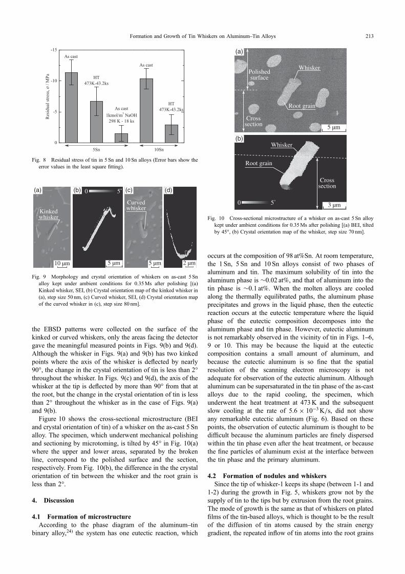
Figure 8 shows the changes in the residual stresses of tin inthe 5 Sn and 10 Sn alloys which underwent the heat treatmentor the sodium hydroxide immersion. While the residualstresses of tin in the as-cast 5 Sn and 10 Sn alloys are nearlyequal (1112MPa), that of tin in the 10 Sn alloy shows agreater decrease with heat treatment compared to the 5 Snalloy. The residual stress of tin in the 5 Sn alloy remarkablydecreased to 1.5MPa with the sodium hydroxide immersion.
3.4 Orientation of whiskerFigure 9 shows the morphology (SEIs) and crystal
orientation of the whiskers on the as-cast 5 Sn alloy. Since
(a)
1-1
2-1
2-r
1-r 20 µm
(b)
1-1 1-2
2-12-r
1-r20 µm
(c)
1-1 1-2
2-12-r
2-2
1-r
20 µm
(d)
1-1
1-2
1-3
2-1
2-r
2-2
1-r20 µm
Fig. 5 Fixed-point observation of as-cast 5 Sn alloy (SEI, (a) Kept underambient conditions for 0.26Ms after polishing, (b) 1.0Ms, (c) 2.7Ms,(d) 7.8Ms).
(a)
100 µm
(b)
Nodule
100 µm
(c)
100 µm
Fig. 6 Fixed-point observation of heat-treated 10 Sn alloy (SEI, (a) As polished, (b) Kept under ambient conditions for 0.60Ms afterpolishing, (c) 7.8Ms).
(a)
20 µm
(b)
20 µm
Fig. 7 Fixed-point observation of as-cast 5 Sn alloy etched in the solution of 1 kmol/m3 sodium hydroxide at 298K for 18 ks (BEI, (a) Asetched, (b) Kept under ambient conditions for 7.7Ms after etching).
K. Murakami, M. Hino, Y. Mitooka and T. Kanadani212
the EBSD patterns were collected on the surface of thekinked or curved whiskers, only the areas facing the detectorgave the meaningful measured points in Figs. 9(b) and 9(d).Although the whisker in Figs. 9(a) and 9(b) has two kinkedpoints where the axis of the whisker is deflected by nearly90°, the change in the crystal orientation of tin is less than 2°throughout the whisker. In Figs. 9(c) and 9(d), the axis of thewhisker at the tip is deflected by more than 90° from that atthe root, but the change in the crystal orientation of tin is lessthan 2° throughout the whisker as in the case of Figs. 9(a)and 9(b).
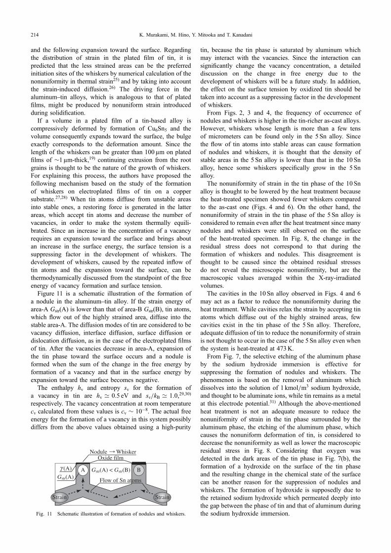
Figure 10 shows the cross-sectional microstructure (BEIand crystal orientation of tin) of a whisker on the as-cast 5 Snalloy. The specimen, which underwent mechanical polishingand sectioning by microtoming, is tilted by 45° in Fig. 10(a)where the upper and lower areas, separated by the brokenline, correspond to the polished surface and the section,respectively. From Fig. 10(b), the difference in the the crystalorientation of tin between the whisker and the root grain isless than 2°.
4. Discussion
4.1 Formation of microstructureAccording to the phase diagram of the aluminumtin
binary alloy,24) the system has one eutectic reaction, which
occurs at the composition of 98 at%Sn. At room temperature,the 1 Sn, 5 Sn and 10 Sn alloys consist of two phases ofaluminum and tin. The maximum solubility of tin into thealuminum phase is ³0.02 at%, and that of aluminum into thetin phase is ³0.1 at%. When the molten alloys are cooledalong the thermally equilibrated paths, the aluminum phaseprecipitates and grows in the liquid phase, then the eutecticreaction occurs at the eutectic temperature where the liquidphase of the eutectic composition decomposes into thealuminum phase and tin phase. However, eutectic aluminumis not remarkably observed in the vicinity of tin in Figs. 16,9 or 10. This may be because the liquid at the eutecticcomposition contains a small amount of aluminum, andbecause the eutectic aluminum is so fine that the spatialresolution of the scanning electron microscopy is notadequate for observation of the eutectic aluminum. Althoughaluminum can be supersaturated in the tin phase of the as-castalloys due to the rapid cooling, the specimen, whichunderwent the heat treatment at 473K and the subsequentslow cooling at the rate of 5.6 © 10¹3K/s, did not showany remarkable eutectic aluminum (Fig. 6). Based on thesepoints, the observation of eutectic aluminum is thought to bedifficult because the aluminum particles are finely dispersedwithin the tin phase even after the heat treatment, or becausethe fine particles of aluminum exist at the interface betweenthe tin phase and the primary aluminum.
4.2 Formation of nodules and whiskersSince the tip of whisker-1 keeps its shape (between 1-1 and
1-2) during the growth in Fig. 5, whiskers grow not by thesupply of tin to the tips but by extrusion from the root grains.The mode of growth is the same as that of whiskers on platedfilms of the tin-based alloys, which is thought to be the resultof the diffusion of tin atoms caused by the strain energygradient, the repeated inflow of tin atoms into the root grains
Fig. 8 Residual stress of tin in 5 Sn and 10 Sn alloys (Error bars show theerror values in the least square fitting).
(a)
Kinkedwhisker
10 µm
(b) 0 5°
5 µm
(c)
Curvedwhisker
5 µm
(d)
2 µm
Fig. 9 Morphology and crystal orientation of whiskers on as-cast 5 Snalloy kept under ambient conditions for 0.35Ms after polishing [(a)Kinked whisker, SEI, (b) Crystal orientation map of the kinked whisker in(a), step size 50 nm, (c) Curved whisker, SEI, (d) Crystal orientation mapof the curved whisker in (c), step size 80 nm].
5 µm
WhiskerPolishedsurface
Crosssection
Root grain
(a)
3 µm
(b)
0 5°
Whisker
Root grain
Crosssection
Fig. 10 Cross-sectional microstructure of a whisker on as-cast 5 Sn alloykept under ambient conditions for 0.35Ms after polishing [(a) BEI, tiltedby 45°, (b) Crystal orientation map of the whisker, step size 70 nm].
Formation and Growth of Tin Whiskers on AluminumTin Alloys 213
and the following expansion toward the surface. Regardingthe distribution of strain in the plated film of tin, it ispredicted that the less strained areas can be the preferredinitiation sites of the whiskers by numerical calculation of thenonuniformity in thermal strain25) and by taking into accountthe strain-induced diffusion.26) The driving force in thealuminumtin alloys, which is analogous to that of platedfilms, might be produced by nonuniform strain introducedduring solidification.
If a volume in a plated film of a tin-based alloy iscompressively deformed by formation of Cu6Sn5 and thevolume consequently expands toward the surface, the bulgeexactly corresponds to the deformation amount. Since thelength of the whiskers can be greater than 100 µm on platedfilms of ³1µm-thick,19) continuing extrusion from the rootgrains is thought to be the nature of the growth of whiskers.For explaining this process, the authors have proposed thefollowing mechanism based on the study of the formationof whiskers on electroplated films of tin on a coppersubstrate.27,28) When tin atoms diffuse from unstable areasinto stable ones, a restoring force is generated in the latterareas, which accept tin atoms and decrease the number ofvacancies, in order to make the system thermally equili-brated. Since an increase in the concentration of a vacancyrequires an expansion toward the surface and brings aboutan increase in the surface energy, the surface tension is asuppressing factor in the development of whiskers. Thedevelopment of whiskers, caused by the repeated inflow oftin atoms and the expansion toward the surface, can bethermodynamically discussed from the standpoint of the freeenergy of vacancy formation and surface tension.
Figure 11 is a schematic illustration of the formation ofa nodule in the aluminumtin alloy. If the strain energy ofarea-A Gstr(A) is lower than that of area-B Gstr(B), tin atoms,which flow out of the highly strained area, diffuse into thestable area-A. The diffusion modes of tin are considered to bevacancy diffusion, interface diffusion, surface diffusion ordislocation diffusion, as in the case of the electroplated filmsof tin. After the vacancies decrease in area-A, expansion ofthe tin phase toward the surface occurs and a nodule isformed when the sum of the change in the free energy byformation of a vacancy and that in the surface energy byexpansion toward the surface becomes negative.
The enthalpy hv and entropy sv for the formation ofa vacancy in tin are hv ’ 0.5 eV and sv/kB ’ 1.0,29,30)
respectively. The vacancy concentration at room temperaturecv calculated from these values is cv ³ 10¹8. The actual freeenergy for the formation of a vacancy in this system possiblydiffers from the above values obtained using a high-purity
tin, because the tin phase is saturated by aluminum whichmay interact with the vacancies. Since the interaction cansignificantly change the vacancy concentration, a detaileddiscussion on the change in free energy due to thedevelopment of whiskers will be a future study. In addition,the effect on the surface tension by oxidized tin should betaken into account as a suppressing factor in the developmentof whiskers.
From Figs. 2, 3 and 4, the frequency of occurrence ofnodules and whiskers is higher in the tin-richer as-cast alloys.However, whiskers whose length is more than a few tensof micrometers can be found only in the 5 Sn alloy. Sincethe flow of tin atoms into stable areas can cause formationof nodules and whiskers, it is thought that the density ofstable areas in the 5 Sn alloy is lower than that in the 10 Snalloy, hence some whiskers specifically grow in the 5 Snalloy.
The nonuniformity of strain in the tin phase of the 10 Snalloy is thought to be lowered by the heat treatment becausethe heat-treated specimen showed fewer whiskers comparedto the as-cast one (Figs. 4 and 6). On the other hand, thenonuniformity of strain in the tin phase of the 5 Sn alloy isconsidered to remain even after the heat treatment since manynodules and whiskers were still observed on the surfaceof the heat-treated specimen. In Fig. 8, the change in theresidual stress does not correspond to that during theformation of whiskers and nodules. This disagreement isthought to be caused since the obtained residual stressesdo not reveal the microscopic nonuniformity, but are themacroscopic values averaged within the X-ray-irradiatedvolumes.
The cavities in the 10 Sn alloy observed in Figs. 4 and 6may act as a factor to reduce the nonuniformity during theheat treatment. While cavities relax the strain by accepting tinatoms which diffuse out of the highly strained areas, fewcavities exist in the tin phase of the 5 Sn alloy. Therefore,adequate diffusion of tin to reduce the nonuniformity of strainis not thought to occur in the case of the 5 Sn alloy even whenthe system is heat-treated at 473K.
From Fig. 7, the selective etching of the aluminum phaseby the sodium hydroxide immersion is effective forsuppressing the formation of nodules and whiskers. Thephenomenon is based on the removal of aluminum whichdissolves into the solution of 1 kmol/m3 sodium hydroxide,and thought to be aluminate ions, while tin remains as a metalat this electrode potential.31) Although the above-mentionedheat treatment is not an adequate measure to reduce thenonuniformity of strain in the tin phase surrounded by thealuminum phase, the etching of the aluminum phase, whichcauses the nonuniform deformation of tin, is considered todecrease the nonuniformity as well as lower the macroscopicresidual stress in Fig. 8. Considering that oxygen wasdetected in the dark areas of the tin phase in Fig. 7(b), theformation of a hydroxide on the surface of the tin phaseand the resulting change in the chemical state of the surfacecan be another reason for the suppression of nodules andwhiskers. The formation of hydroxide is supposedly due tothe retained sodium hydroxide which permeated deeply intothe gap between the phase of tin and that of aluminum duringthe sodium hydroxide immersion.
(A) A BGstr(A) < Gstr(B)γGstr(A)
Strain Strain
Nodule
Flow of Sn atoms
Oxide filmWhisker
Fig. 11 Schematic illustration of formation of nodules and whiskers.
K. Murakami, M. Hino, Y. Mitooka and T. Kanadani214
For the electroplated film of the tin-based alloy on thecopper substrate, only nodules are extensively formed onthe surface when the oxide film is removed by etching withargon ion in an ultra-high vacuum (³10¹8 Pa), and when theargon ion-etched specimen is then kept in the vacuumchamber.27,28) On the other hand, the development of nodulesand whiskers is suppressed in an environment of highertemperature and humidity (333K, relative himidity 90%)compared to ambient conditions.32) Based on these results,the chemical treatment of the aluminumtin alloys is thoughtto effectively suppress whiskers since the treatment modifiesthe chemical state of the surface or the surface tension,and selectively etches the aluminum phase to reduce thenonuniformity of strain in the tin phase. Other knownprocesses for the suppression of whiskers on the jointsinclude rinsing in solutions of phosphoric or boric acidat high temperature and the implantation of phosphorusions.2,47,33) The rinse, performed at ³363K, might act as aheat treatment which changes the microstructure and thestrain distribution. However, the sodium hydroxide immer-sion in this study was performed at 298K. That is, theselective etching of aluminum and the appropriate modifica-tion of the chemical state on the surface at room temperatureare thought to be highly effective for the suppression ofwhiskers.
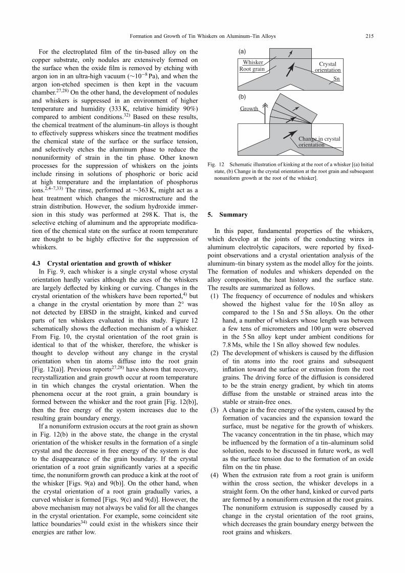
4.3 Crystal orientation and growth of whiskerIn Fig. 9, each whisker is a single crystal whose crystal
orientation hardly varies although the axes of the whiskersare largely deflected by kinking or curving. Changes in thecrystal orientation of the whiskers have been reported,4) buta change in the crystal orientation by more than 2° wasnot detected by EBSD in the straight, kinked and curvedparts of ten whiskers evaluated in this study. Figure 12schematically shows the deflection mechanism of a whisker.From Fig. 10, the crystal orientation of the root grain isidentical to that of the whisker, therefore, the whisker isthought to develop without any change in the crystalorientation when tin atoms diffuse into the root grain[Fig. 12(a)]. Previous reports27,28) have shown that recovery,recrystallization and grain growth occur at room temperaturein tin which changes the crystal orientation. When thephenomena occur at the root grain, a grain boundary isformed between the whisker and the root grain [Fig. 12(b)],then the free energy of the system increases due to theresulting grain boundary energy.
If a nonuniform extrusion occurs at the root grain as shownin Fig. 12(b) in the above state, the change in the crystalorientation of the whisker results in the formation of a singlecrystal and the decrease in free energy of the system is dueto the disappearance of the grain boundary. If the crystalorientation of a root grain significantly varies at a specifictime, the nonuniform growth can produce a kink at the root ofthe whisker [Figs. 9(a) and 9(b)]. On the other hand, whenthe crystal orientation of a root grain gradually varies, acurved whisker is formed [Figs. 9(c) and 9(d)]. However, theabove mechanism may not always be valid for all the changesin the crystal orientation. For example, some coincident sitelattice boundaries34) could exist in the whiskers since theirenergies are rather low.
5. Summary
In this paper, fundamental properties of the whiskers,which develop at the joints of the conducting wires inaluminum electrolytic capacitors, were reported by fixed-point observations and a crystal orientation analysis of thealuminumtin binary system as the model alloy for the joints.The formation of nodules and whiskers depended on thealloy composition, the heat history and the surface state.The results are summarized as follows.(1) The frequency of occurrence of nodules and whiskers
showed the highest value for the 10 Sn alloy ascompared to the 1 Sn and 5 Sn alloys. On the otherhand, a number of whiskers whose length was betweena few tens of micrometers and 100 µm were observedin the 5 Sn alloy kept under ambient conditions for7.8Ms, while the 1 Sn alloy showed few nodules.
(2) The development of whiskers is caused by the diffusionof tin atoms into the root grains and subsequentinflation toward the surface or extrusion from the rootgrains. The driving force of the diffusion is consideredto be the strain energy gradient, by which tin atomsdiffuse from the unstable or strained areas into thestable or strain-free ones.
(3) A change in the free energy of the system, caused by theformation of vacancies and the expansion toward thesurface, must be negative for the growth of whiskers.The vacancy concentration in the tin phase, which maybe influenced by the formation of a tinaluminum solidsolution, needs to be discussed in future work, as wellas the surface tension due to the formation of an oxidefilm on the tin phase.
(4) When the extrusion rate from a root grain is uniformwithin the cross section, the whisker develops in astraight form. On the other hand, kinked or curved partsare formed by a nonuniform extrusion at the root grains.The nonuniform extrusion is supposedly caused by achange in the crystal orientation of the root grains,which decreases the grain boundary energy between theroot grains and whiskers.
Root grain
Sn
Whisker
(a)
Crystalorientation
(b)
Growth
Change in crystalorientation
Fig. 12 Schematic illustration of kinking at the root of a whisker [(a) Initialstate, (b) Change in the crystal orientation at the root grain and subsequentnonuniform growth at the root of the whisker].
Formation and Growth of Tin Whiskers on AluminumTin Alloys 215
(5) The aluminum phase is thought to nonuniformlydeform the contacting tin phase. The formation ofnodules and whiskers were suppressed by the selectiveetching of the aluminum phase in the solution ofsodium hydroxide. The change in the chemical state ofthe surface caused by the chemical treatment, or that inthe surface tension, can influence the behavior of thewhiskers.
REFERENCES
1) T. Kubouchi and O. Kamiya: J. Soc. Mater. Eng. Res. Jpn. 23 (2010)1318 (in Japanese).
2) K. Matsuzawa and Y. Makino: Proc. 34th Symp. on Reliability andMaintainability, (Union of Japanese Scientists and Engineers, Tokyo,Japan, 2004) pp. 103108 (in Japanese).
3) K. Kumagai, Y. Kawahito, T. Hirooka and Y. Ihara: IEICE Tech. Rep.,R, Reliability, R2007-55, SSS2007-28 (2007) pp. 510 (in Japanese).
4) Y. Kawahito, K. Kumagai, T. Hirooka and Y. Ihara: Proc. 38th Symp.on Reliability and Maintainability, (Union of Japanese Scientists andEngineers, Tokyo, Japan, 2008) pp. 153158 (in Japanese).
5) JEITA namari-free-ka-katsudou-seika-houkokukai 2008: Japan Elec-tronics and Information Technology Industries Association, (electronicspackaging standardization committee, 2008) pp. 4150 (in Japanese).
6) JEITA namari-free-ka-katsudou-seika-houkokukai 2009: Japan Elec-tronics and Information Technology Industries Association, (electronicspackaging standardization committee, 2009) pp. 5969 (in Japanese).
7) Research report of heisei-20-nendo senryaku-teki-kiban-gijutu-koudo-ka-shien-jigyou, denshi-jissou-no-shinrai-sei-koujou-no-tame-no-whisker-boushi-gijutsu-no-kaihatsu, http://www.smrj.go.jp/keiei/dbps_data/_material_/common/chushou/b_keiei/keieitech/pdf/jeita21.pdf,(Organization for Small and Medium Enterprises and RegionalInnovation, Japan, 2009) (in Japanese).
8) R. Kawanaka, Y. Fujiwara, K. Tsuji, S. Ito and Y. Ihara: Suzu-whisker-seichou-process-no-kaimei-to-taisaku, (R&D Planning, 2006) p. 3(in Japanese).
9) K. Suganuma: J. Surf. Fin. Soc. Jpn. 59 (2008) 210217 (in Japanese).10) T. Asai, T. Kiga, Y. Taniguchi, H. Morikawa and K. Sumiyama: J. Jpn.
Inst. Metals 73 (2009) 823832 (in Japanese).11) T. Kakeshita, K. Shimizu, R. Kawanaka and T. Hasegawa: J. Mater.
Sci. 17 (1982) 25602566.12) Q. Yu, T. Shibutani, S. Hokazono and Y. Kusunoki: Kino Zairyo 28
(2008) 2025 (in Japanese).13) K. Kim, K. Suganuma, M. Tsujimoto and I. Yanada: Kino Zairyo 28
(2008) 2631 (in Japanese).14) K. N. Tu: Acta Metall. 21 (1973) 347354.15) B.-Z. Lee and D. N. Lee: Acta Mater. 46 (1998) 37013714.16) G. T. Galyon: IEEE Trans. Electron. Pack. Manufact. 28 (2005) 94
122.17) W. J. Böttinger, C. E. Johnson, L. A. Bendersky, K. W. Moon, M. E.
Williams and G. R. Stafford: Acta Mater. 53 (2005) 50335050.18) T. Kato, H. Akahoshi, M. Nakamura, T. Hashimoto and A. Nishimura:
IEEE Trans. Electron. Pack. Manufact. 30 (2007) 258269.19) K. Tsuji: J. Surf. Fin. Soc. Jpn. 58 (2007) 406411 (in Japanese).20) M. Sobiech, U. Welzel, E. J. Mittemeijer, W. Hügel and A. Seekamp:
Appl. Phys. Lett. 93 (2008) 011906.21) T. Kato, H. Akahoshi, M. Nakamura, T. Iwasaki, T. Hashimoto and A.
Nishimura: IEEE Trans. Electron. Pack. Manufact. 33 (2010) 165176.22) A. Sato: J. Surf. Fin. Soc. Jpn. 57 (2006) 554558 (in Japanese).23) B. B. He, X. L. Wang, W. Tang and Y. Chao: Proc. 2001 SEM Spring
Conf. on Experimental and Applied Mechanics, Portland, Oregon,USA, (2001) pp. 547550.
24) A. J. McAlister: Binary Alloy Phase Diagrams, Second Edition, ed.by T. B. Massalski, (ASM International, Ohio, USA, 1990) pp. 215216.
25) J.-H. Zhao, P. Su, M. Ding, S. Chopin and P. S. Ho: IEEE Trans.Electron. Pack. Manufact. 29 (2006) 265273.
26) T. Terasaki, T. Iwasaki, Y. Okura, T. Suzuki, T. Kato, M. Nakamura andT. Hashimoto: 2009 IEEE 59th Electronic Components and TechnologyConference, (IEEE, San Diego, California, USA, 2009) pp. 277284.
27) K. Murakami, M. Hino, M. Takamizawa and K. Nakai: J. Jpn. Inst.Metals 72 (2008) 168175 (in Japanese).
28) K. Murakami, M. Hino, M. Takamizawa and K. Nakai: Mater. Trans.49 (2008) 28292836.
29) R. Balzer and H. Sigvaldason: Phys. Stat. Sol. (B) 92 (1979) 143147.30) D. Segers, L. Dorikens-Vanpraet and M. Dorikens: Phys. Stat. Sol. (A)
59 (1980) 543546.31) M. Pourbaix: Atlas of Electrochemical Equilibria in Aqueous Solutions,
(National Association of Corrosion Engineers, Houston, Texas, USA,1974) pp. 475484.
32) M. Hino, K. Murakami and Y. Mitooka: J. Surf. Fin. Soc. Jpn. 62(2011) 4146 (in Japanese).
33) F. Ishii, S. Yoshizawa and N. Araki: Japan patent 2007-220804 (2007)(in Japanese).
34) T. Heumann and H. Mehrer: Diffusion in Metllen, translated byS. Fujikawa, (Springer-Verlag, Tokyo, Japan, 2005) pp. 300306(in Japanese).
K. Murakami, M. Hino, Y. Mitooka and T. Kanadani216