Embed Size (px)
Citation preview
Growth Mechanisms of Tin Whiskers at Press-in Technology
Hans-Peter Tranitz1,a
and Sebastian Dunker2,
1Continental Automotive GmbH, D-93055 Regensburg, Germany
2Conti Temic microelectronic GmbH, D-90411 Nuremberg, Germany
Abstract
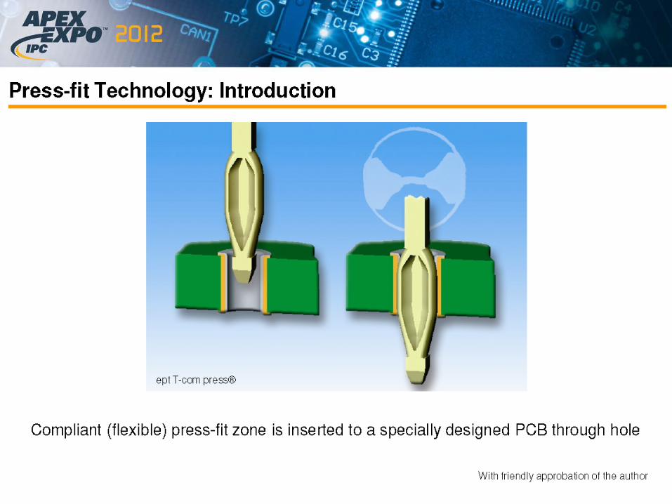
Compliant press-fit zones apply external mechanical stress to copper and tin surfaces of plated through holes at
printed circuit boards during and after performing the press-in process. This external pressure increases the tendency
to create tin whiskers. These whiskers grow on much shorter time scales than whiskers caused by strain introduced
by intermetallic phase growth. Also the length of these whiskers can exceed 2 mm under special circumstances and
cause malfunction of electronic circuits. The results shown in this paper support the understanding for the growth
mechanisms at different geometrical shapes of press-fit zones and therefore give strong impact on the risk analysis.
Introduction
A large number of studies about whiskers grown by intermetallic phase growth have been performed and collected
for the convenience of the scientific and applied research community at the NASA tin whisker homepage [1].
Recently, very detailed studies about the driving forces of whisker growth and micro-scaled strain gradients as well
as their relevance for whisker formation have been published [2-4]. Besides, it has been published that other
material combinations causing lateral stress, e.g. in phase separating Si-Sn systems, show the growth of Sn
nanowires varying in density, length and diameter as a function of the Si and Sn contents [5]. All these publications
strongly contribute to the understanding of the whisker formation as a consequence of inner surface strain relieve.
Theoretical models have been developed to describe and predict the whisker formation behavior [6, 7] and are in
good alignment with specially performed experiments [8]. Less is known about the formation of whiskers driven by
external mechanical stress even if first publications appeared already in the 50th
[9].
More recently, international standardization efforts are ongoing to support the evaluation of whisker growth by
external stress [10]. This paper describes whisker growth in plastically deformed chemical tin plated copper
bushings of a plated through hole in standard FR4 printed circuit boards. The deformation is induced by the
insertion of different compliant press-in zones. Degree and shape of this deformation differs with the geometry of
these tin coated press-fit geometries. The induced stress to the surface of the bushing is large enough to initiate tin
whisker growth. These whiskers occur within days reaching lengths of several hundred micrometers. Such stress
induced whisker nucleation and growth process is described in [11] and fits well to our observations.
Sample build-up and experimental setup
Ten different compliant press-fit pins qualified for the same design of press-in plated-through holes have been
investigated according to their whisker behavior. The zone types have been delivered by different suppliers
supporting this project and their product for this study. All press-fit zones are made out of a standard copper alloy
base material such as CuSn(4-6) bronze with 0,6 mm thickness of the stamping band. The stamped samples have
been electroplated with a 1 µm Ni barrier layer and a 1 µm Sn surface finish. All tin galvanic chemistry used for this
study is resulting in a matt tin surface and the chemistries are supposed to be whisker mitigating. Due to the selected
set-up of Ni underlayer and matt tin surface the probability of surface whisker growth in the time frames of this work
is minimized and can be neglected. 300 of each zone type have been inserted mostly by the suppliers themselves or
by the authors according to supplier’s specifications respecting international standards [12]. The used printed circuit
boards (PCBs) have been coated with 1 µm chemical tin. Those series production PCBs have been designed with an
array of press-fit through holes each of 1,05-1,08 mm final hole diameter (used drill bit 1,15 mm, copper layer about
30µm). For preconditioning, the PCBs have been put to a single standard reflow process for Pb-containing solder
a Author to whom correspondence may be addressed: [email protected]
paste representing the case for the maximum remaining free Sn thickness on the board assuming that this will be also
the environment for maximum whisker formation. The build-up samples have been stored for 6 weeks under
uncontrolled ambient conditions in a cabinet. Relative humidity and temperature has been recorded to be 40 ± 4 %
and 23 ± 1 °C during the storage time. In accordance to our observations it has been published recently [11] that the
growth of these external stress whiskers is saturating within this timeframe. Following, the samples have been
inspected according to their whisker growth. Therefore the assembled boards have been investigated using a
metallurgical microscope with 50x magnification. The exit side of the press-in pins (tip of the press-fit zone) shows
in the direction of the objective. The set-up has been illuminated from the entrance side in incident light geometry.
Scrolling the focus plane through the bushing, the shadow of the whiskers can be detected. This projection of the
whiskers has been imaged with a digital camera and the length of the whisker has been measured in x-y plane. An
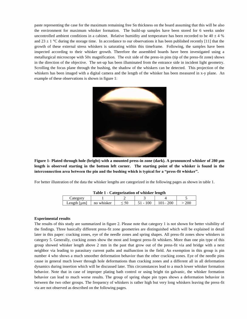
example of these observations is shown in figure 1:
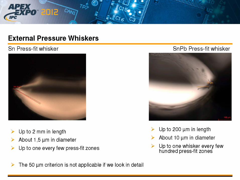
Figure 1- Plated through hole (bright) with a mounted press-in zone (dark). A pronounced whisker of 280 µm
length is observed starting in the bottom left corner. The starting point of the whisker is found in the
interconnection area between the pin and the bushing which is typical for a “press-fit whisker”.
For better illustration of the data the whisker lengths are categorized in the following pages as shown in table 1.
Table 1 - Categorization of whisker length
Category 1 2 3 4 5
Length [µm] no whisker ≤ 50 51 - 100 101– 200 > 200
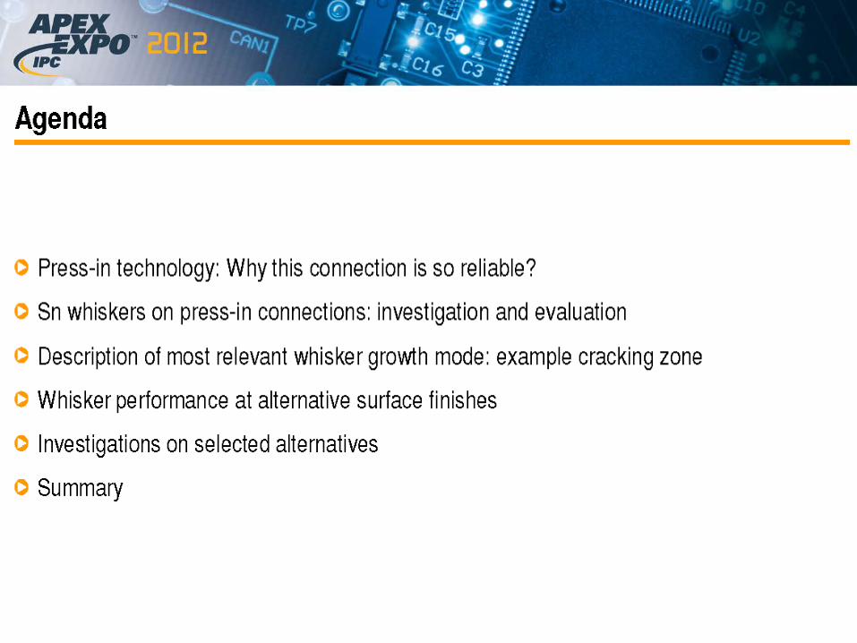
Experimental results
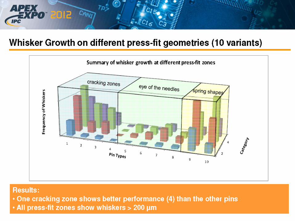
The results of this study are summarized in figure 2. Please note that category 1 is not shown for better visibility of
the findings. Three basically different press-fit zone geometries are distinguished which will be explained in detail
later in this paper: cracking zones, eye of the needle zones and spring shapes. All press-fit zones show whiskers in
category 5. Generally, cracking zones show the most and longest press-fit whiskers. More than one pin type of this
group showed whisker length above 2 mm in the past that grow out of the press-fit via and bridge with a next
neighbor via leading to parasitary current paths and malfunction in the field. An exemption in this group is pin
number 4 who shows a much smoother deformation behavior than the other cracking zones. Eye of the needle pins
cause in general much lower through hole deformations than cracking zones and a different all in all deformation
dynamics during insertion which will be discussed later. This circumstances lead to a much lower whisker formation
behavior. Note that in case of improper plating bath control or using bright tin galvanic, the whisker formation
behavior can lead to much worse results. The group of spring shape pin types shows a deformation behavior in
between the two other groups. The frequency of whiskers is rather high but very long whiskers leaving the press-fit
via are not observed as described on the following pages.
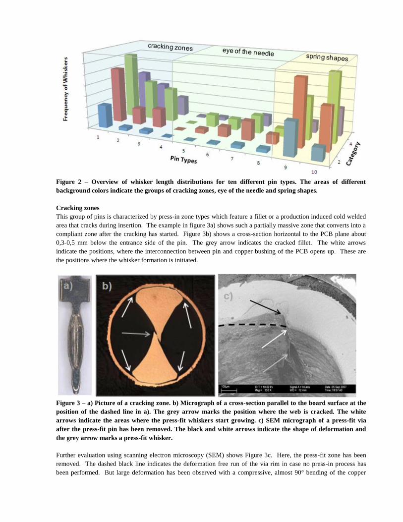
Figure 2 – Overview of whisker length distributions for ten different pin types. The areas of different
background colors indicate the groups of cracking zones, eye of the needle and spring shapes.
Cracking zones
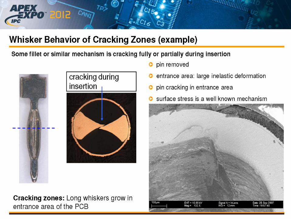
This group of pins is characterized by press-in zone types which feature a fillet or a production induced cold welded
area that cracks during insertion. The example in figure 3a) shows such a partially massive zone that converts into a
compliant zone after the cracking has started. Figure 3b) shows a cross-section horizontal to the PCB plane about
0,3-0,5 mm below the entrance side of the pin. The grey arrow indicates the cracked fillet. The white arrows
indicate the positions, where the interconnection between pin and copper bushing of the PCB opens up. These are
the positions where the whisker formation is initiated.
Figure 3 – a) Picture of a cracking zone. b) Micrograph of a cross-section parallel to the board surface at the
position of the dashed line in a). The grey arrow marks the position where the web is cracked. The white
arrows indicate the areas where the press-fit whiskers start growing. c) SEM micrograph of a press-fit via
after the press-fit pin has been removed. The black and white arrows indicate the shape of deformation and
the grey arrow marks a press-fit whisker.
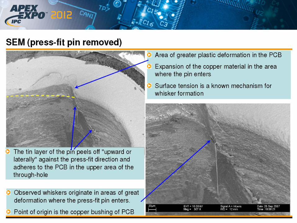
Further evaluation using scanning electron microscopy (SEM) shows Figure 3c. Here, the press-fit zone has been
removed. The dashed black line indicates the deformation free run of the via rim in case no press-in process has
been performed. But large deformation has been observed with a compressive, almost 90° bending of the copper
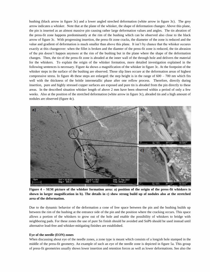
bushing (black arrow in figure 3c) and a lower angled streched deformation (white arrow in figure 3c). The grey
arrow indicates a whisker. Note that at the plane of the whisker, the shape of deformation changes: Above this plane,
the pin is inserted as an almost massive pin causing rather large deformation values and angles. The tin abration of
the press-fit zone happens predominantly at the rim of the bushing which can be observed also close to the black
arrow of figure 3c. With progressing insertion, the press-fit zone cracks, the diameter of the zone is reduced and the
value and gradient of deformation is much smaller than above this plane. It isn’t by chance that the whisker occures
exactly at this changeover: when the fillet is broken and the diamter of the press-fit zone is reduced, the tin abrasion
of the pin doesn’t happen anymore at the rim of the bushing but in the plane where the shape of the deformation
changes. Then, the tin of the press-fit zone is abraded at the inner wall of the through hole and delivers the material
for the whiskers. To explain the origin of the whisker formation, more detailed investigation explained in the
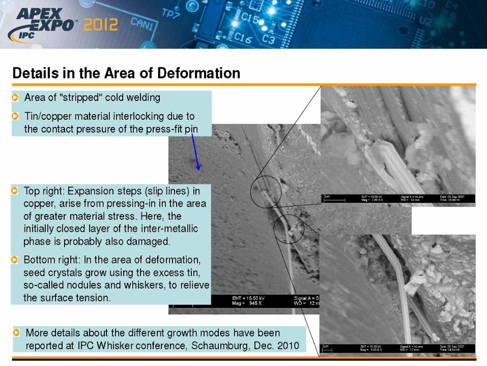
following sentences is necessary. Figure 4a shows a magnification of the whisker in figure 3c. At the footpoint of the
whisker steps in the surface of the bushing are observed. Those slip lines occure at the deformation areas of highest
compressive stress. In figure 4b these steps are enlarged: the step height is in the range of 600 – 700 nm which fits
well with the thickness of the brittle intermetallic phase after one reflow process. Therefore, directly during
insertion, pure and highly stressed copper surfaces are exposed and pure tin is abraded from the pin directly to these
areas. In the described situation whisker length of above 2 mm have been observed within a period of only a few
weeks. Also at the position of the stretched deformation (white arrow in figure 3c), abraded tin and a high amount of
nodules are observed (figure 4c).
Figure 4 – SEM picture of the whisker formation area: a) position of the origin of the press-fit whiskers is
shown in larger magnification in b). The details in c) show strong build up of nodules also at the stretched
area of the deformation.
Due to the dynamic behavior of the deformation a cone of free space between the pin and the bushing builds up
between the rim of the bushing at the entrance side of the pin and the position where the cracking occurs. This space
allows a portion of the whiskers to grow out of the hole and enable the possibility of whiskers to bridge with
neighboring pads. For these zones the use of pure Sn finish should be avoided and SnPb should be used instead until
alternative lead-free and whisker-mitigating finishes are established.
Eye of the needle (EON) zones
When discussing about eye of the needle zones, a zone type is meant which consists of a longish hole stamped in the
middle of the press-fit geometry. An example of such an eye of the needle zone is depicted in figure 5a. This group
of press-fit geometries usually shows lower insertion and retention forces as well as lower deformations. See also the
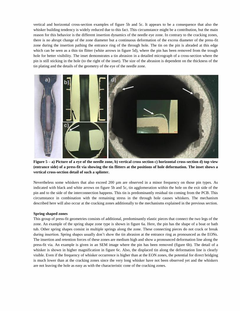
vertical and horizontal cross-section examples of figure 5b and 5c. It appears to be a consequence that also the
whisker building tendency is widely reduced due to this fact. This circumstance might be a contribution, but the main
reason for this behavior is the different insertion dynamics of the needle eye zone. In contrary to the cracking zones,
there is no abrupt change of the zone diameter but a continuous deformation of the excess diameter of the press-fit
zone during the insertion pathing the entrance ring of the through hole. The tin on the pin is abraded at this edge
which can be seen as a thin tin flitter (white arrows in figure 5d), where the pin has been removed from the trough
hole for better visibility. The inset demonstrates a tin abrasion in a detailed micrograph of a cross-section where the
pin is still sticking in the hole (to the right of the inset). The size of the abrasion is dependent on the thickness of the
tin plating and the details of the geometry of the eye of the needle zone.
Figure 5 – a) Picture of a eye of the needle zone, b) vertical cross section c) horizontal cross-section d) top view
(entrance side) of a press-fit via showing the tin flitters at the positions of hole deformation. The inset shows a
vertical cross-section detail of such a splinter.
Nevertheless some whiskers that also exceed 200 µm are observed in a minor frequency on those pin types. As
indicated with black and white arrows on figure 5b and 5c, tin agglomeration within the hole on the exit side of the
pin and to the side of the interconnection happens. This tin is predominantly residual tin coming from the PCB. This
circumstance in combination with the remaining stress in the through hole causes whiskers. The mechanism
described here will also occur at the cracking zones additionally to the mechanisms explained in the previous section.
Spring shaped zones
This group of press-fit geometries consists of additional, predominantly elastic pieces that connect the two legs of the
zone. An example of the spring shape zone type is shown in figure 6a. Here, the pin has the shape of a boat or bath
tub. Other spring shapes consist in multiple springs along the zone. These connecting pieces do not crack or break
during insertion. Spring shapes usually don’t show the tin abrasion at the entrance ring as pronounced as the EONs.
The insertion and retention forces of these zones are medium high and show a pronounced deformation line along the
press-fit via. An example is given in an SEM image where the pin has been removed (figure 6b). The detail of a
whisker is shown in higher magnification in figure 6c. Also, the displaced tin along the deformation line is clearly
visible. Even if the frequency of whisker occurrence is higher than at the EON zones, the potential for direct bridging
is much lower than at the cracking zones since the very long whisker have not been observed yet and the whiskers
are not leaving the hole as easy as with the characteristic cone of the cracking zones.
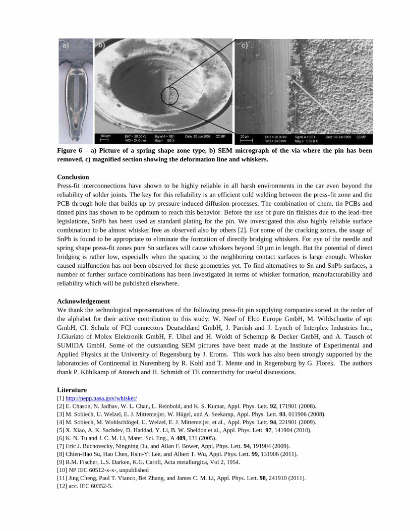
Figure 6 – a) Picture of a spring shape zone type, b) SEM micrograph of the via where the pin has been
removed, c) magnified section showing the deformation line and whiskers.
Conclusion
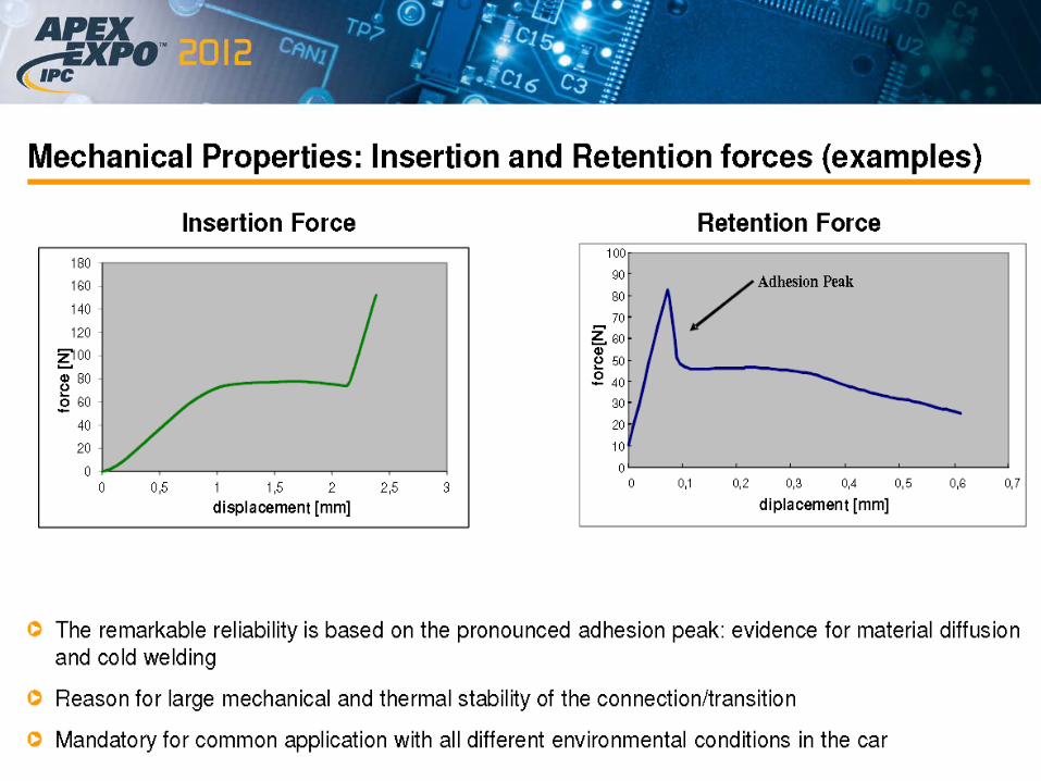
Press-fit interconnections have shown to be highly reliable in all harsh environments in the car even beyond the
reliability of solder joints. The key for this reliability is an efficient cold welding between the press-fit zone and the
PCB through hole that builds up by pressure induced diffusion processes. The combination of chem. tin PCBs and
tinned pins has shown to be optimum to reach this behavior. Before the use of pure tin finishes due to the lead-free
legislations, SnPb has been used as standard plating for the pin. We investigated this also highly reliable surface
combination to be almost whisker free as observed also by others [2]. For some of the cracking zones, the usage of
SnPb is found to be appropriate to eliminate the formation of directly bridging whiskers. For eye of the needle and
spring shape press-fit zones pure Sn surfaces will cause whiskers beyond 50 µm in length. But the potential of direct
bridging is rather low, especially when the spacing to the neighboring contact surfaces is large enough. Whisker
caused malfunction has not been observed for these geometries yet. To find alternatives to Sn and SnPb surfaces, a
number of further surface combinations has been investigated in terms of whisker formation, manufacturability and
reliability which will be published elsewhere.
Acknowledgement
We thank the technological representatives of the following press-fit pin supplying companies sorted in the order of
the alphabet for their active contribution to this study: W. Neef of Elco Europe GmbH, M. Wildschuette of ept
GmbH, Cl. Schulz of FCI connectors Deutschland GmbH, J. Parrish and J. Lynch of Interplex Industries Inc.,
J.Giuriato of Molex Elektronik GmbH, F. Uibel and H. Woldt of Schempp & Decker GmbH, and A. Tausch of
SUMIDA GmbH. Some of the outstanding SEM pictures have been made at the Institute of Experimental and
Applied Physics at the University of Regensburg by J. Eroms. This work has also been strongly supported by the
laboratories of Continental in Nuremberg by R. Kohl and T. Mente and in Regensburg by G. Florek. The authors
thank P. Kühlkamp of Atotech and H. Schmidt of TE connectivity for useful discussions.
Literature
[1] http://nepp.nasa.gov/whisker/
[2] E. Chason, N. Jadhav, W. L. Chan, L. Reinbold, and K. S. Kumar, Appl. Phys. Lett. 92, 171901 (2008).
[3] M. Sobiech, U. Welzel, E. J. Mittemeijer, W. Hügel, and A. Seekamp, Appl. Phys. Lett. 93, 011906 (2008).
[4] M. Sobiech, M. Wohlschlögel, U. Welzel, E. J. Mittemeijer, et al., Appl. Phys. Lett. 94, 221901 (2009).
[5] X. Xiao, A. K. Sachdev, D. Haddad, Y. Li, B. W. Sheldon et al., Appl. Phys. Lett. 97, 141904 (2010).
[6] K. N. Tu and J. C. M. Li, Mater. Sci. Eng., A 409, 131 (2005).
[7] Eric J. Buchovecky, Ningning Du, and Allan F. Bower, Appl. Phys. Lett. 94, 191904 (2009).
[8] Chien-Hao Su, Hao Chen, Hsin-Yi Lee, and Albert T. Wu, Appl. Phys. Lett. 99, 131906 (2011).
[9] R.M. Fischer, L.S. Darken, K.G. Caroll, Acta metallurgica, Vol 2, 1954.
[10] NP IEC 60512-x-x-, unpublished
[11] Jing Cheng, Paul T. Vianco, Bei Zhang, and James C. M. Li, Appl. Phys. Lett. 98, 241910 (2011).
[12] acc. IEC 60352-5.
•Whiskers and Alternative Surface Finishes at Press-in Technology
•Dr. Hans-Peter Tranitz
•IPC APEX EXPO, Feb. 28 2012, San Diego, USA


•23 / Dr. Hans-Peter Tranitz/ © Continental AG
•Thank you for your attention!