Embed Size (px)
Citation preview

【 】 Finally Specification
CUSTOMER'S APPROVAL
SIGNATURE: DATE:
APPROVED PM PD PREPAREDBY REVIEWD REVIEWD BY
Kam / Stephen Roy
Prepared By :
FORMIKE ELECTRONIC CO.,LTD Address :Room A818 New Energy Building, NanHai Road, NanShan District, ShenZhen, China. 518054
TEL:(86) 755 88306921,88306931 FAX:(86) 755 88304615 Http:// www.wandisplay.com
This specification is subject to change without notice.Please contact FORMIKE or it's representative before designing your product based on this specification.
1 Issued Date:Jan-22-2010
【 】 Preliminary Specification
FORMIKE ELECTRONIC CO.,LTD
PRODUCT SPECIFICATION
TFT LCD MODULEMODEL : KWH018TG02-F01 Ver 1.0

CONTENTS PAGE
Coverpage 1
Record of Revision 3
General Specifications 4
Input/Output Terminals 5
Absolute Maximum Ratings 7
Electrical Characteristics 8
Timing Chart 11
Optical Characteristics 20
Environmental & Reliability Test 24
Mechanical Drawing 25
Packing Information 26
Precautions For Use of LCD Modules 27
TABLE OF CONTENTS
Module No.KWH018TG02-F01FORMIKE ELECTRONIC CO.,LTD_____________________________________________________________________________________
2

Record of Revision
Rev Issued Date Description Editor
1.0 2010-1-22 Preliminary Specification Release Stephen
3
Module No.KWH018TG02-F01FORMIKE ELECTRONIC CO.,LTD_____________________________________________________________________________________

1 General Specification
Feature Description
Size 1.77 inch Display Mode Normally White, TransmissiveTechnology Type a-Si, Clear Type(3H) Resolution 128(RGB) x 160 Interface CPU 8bits/SPI Color Depth 65/262K Pixel Pitch (mm) 0.219x0.219 Pixel Configuration R.G.B. Vertical Stripe Viewing Direction 6 o’clock Gray Scale Inversion Direction 12 o’clock LCM (W x H x D) (mm) 34.0x47.0x2.4 Active Area(mm) 28.032x35.04 With/Without TSP Without TSP Weight (g) TBD LED Numbers 1 LED Driver IC HX8353D
Operation -20~+70Storage -30~+80
Note : Viewing direction for best image quality is different from TFT definition. There is a 180 degree shift.
Tempreture
Module No.KWH018TG02-F01FORMIKE ELECTRONIC CO.,LTD_____________________________________________________________________________________
4

2 Input/Output Terminals 2.1 TFT LCD Panel
No Symbol I/O Description Comment1 LED1+ P LED anode 2 LED2+ P NC 3 LED- P LED cathode
4 IM2 I MCU Parallel interface bus and Serial interface select IM2=’1’, Parallel interface IM2=’0’, Serial interface
5 NRES I Reset Pin 6 DB7 I 7 DB6 I 8 DB5 I 9 DB4 I
10 DB3 I 11 DB2 I 12 DB1 I
Data input, In serial interface, they are not used and should be fixed at VCI or DGND level.
13 DB0/SDI I Data input, when SPI interface, as SDI 14 NC - No connection 15 NC - No connection 16 NC - No connection 17 NC - No connection 18 NC - No connection 19 NC - No connection 20 NC - No connection 21 NC - No connection
22 NRD I Read strobe in 8080 MCU parallel interface. -If not used, please fix this pin at VCI or DGND level.
23 NWR I -Write enable in MCU parallel interface. -In 4-line SPI, this pin is used as D/CX (data/ command selection). -If not used, please fix this pin at VCI or DGND level.
24 RS I
-Display data/command selection pin in MCU interface. - RS =’1’: display data or parameter. - RS =’0’: command data. -In serial interface, this is used as SCL.
25 NCS I Chip select
26 ID O ID Pin R1=215K,R2=47K,VID=0.502V(VCC=2.8V)
27 VCI P Power supply
5
Module No.KWH018TG02-F01FORMIKE ELECTRONIC CO.,LTD_____________________________________________________________________________________

28 SPI4W I - SPI4W=’0’, 3-line SPI enable. - SPI4W=’1’, 4-line SPI enable. -If not used, please fix this pin at DGND level.
29 XR I/O NC 30 YD I/O NC 31 XL I/O NC 32 YU I/O NC 33 GND P GND
Note1: I/O definition: I-----Input O---Output P----Power/Ground
6
Module No.KWH018TG02-F01FORMIKE ELECTRONIC CO.,LTD_____________________________________________________________________________________

3 Absolute Maximum Ratings
3.1 Driving TFT LCD Panel GND=0V, Ta = 25
Item Symbol MIN MAX Unit Remark Logic Supply Voltage VCI -0.3 3.6 V
Analog Supply Voltage VCI -0.3 3.6 V
Input voltage D8~D15,NCS,RS,NWR,NRD NRES,IM2, SPI4W -0.3 VCI+0.3 V
Back Light Forward Current ILED 20 mA For each
LED Operating
Temperature TOPR -20 70
Storage Temperature TSTG -30 80
7
Module No.KWH018TG02-F01FORMIKE ELECTRONIC CO.,LTD_____________________________________________________________________________________

4 Electrical Characteristics 4.1 Driving TFT LCD Panel GND=0V, Ta=25
Item Symbol MIN TYP MAX Unit Remark
Logic Supply Voltage VCI 2.3 2.8 3.3 V
Analog Supply Voltage VCI 2.3 2.8 3.3 V
Low Level VIL -0.3 -- 0.2xVCI V Input Signal Voltage
High Level VIH 0.8xVCI -- VCI V
D8~D15,NCS,RS,NWR,NRD,NRES,IM2, SPI4W
Low Level VOL -- -- 0.2xVCI V Output Signal Voltage
High Level VOH 0.8xVCI -- -- V
Black Mode (60Hz)
-- TBD -- -
Standby Mode
-- TBD -- -- (Panel+ LSI)
Power Consumption
Sleeping Mode
-- TBD -- --
8
Module No.KWH018TG02-F01FORMIKE ELECTRONIC CO.,LTD_____________________________________________________________________________________

4.2 Driving Backlight Ta=25
Item Symbol Min Typ Max Unit Remark Forward Current IF -- 20 -- mA Forward Voltage VF -- 3.2 -- V Backlight Power Consumption
WBL -- 64 -- mW 1 LEDs
Operating Life Time - 10000 (20000) - Hrs For each LED
Note 1: The figure below shows the connection of backlight LED.
Note 2: One LED : IF =20 mA, VF =3.2V Note 3: : IF is defined for one channel LED.
Optical performance should be evaluated at Ta=25 only. If LED is driven by high current, high ambient temperature & humidity condition. The life time of LED will be reduced. Operating life means brightness goes down to 50% initial brightness. Typical operating life time is estimated data.
9
Module No.KWH018TG02-F01FORMIKE ELECTRONIC CO.,LTD_____________________________________________________________________________________

4.3 Block Diagram
VCI GND
1.77 inch 128 (RGB) X160
Source+ Gate Driver
LCD PANEL
Data Bus
CPU I/F
RAM
Grayscale Manipulation Voltage
VCOM& TCON
DC/DC FPC
D8~D15
LCD Driver Chip (COG)
NRD, NRES, IM2
NCS, RS, NWR,
BLU LED-, LED1+
10
Module No.KWH018TG02-F01FORMIKE ELECTRONIC CO.,LTD_____________________________________________________________________________________
5 Timing Chart(Parallel interface) 5.1 Timing Chart(Parallel interface)
5.1.1Timing Parameter
Table 5.1 timing parameter
i80 System Bus Timing
11
Module No.KWH018TG02-F01FORMIKE ELECTRONIC CO.,LTD_____________________________________________________________________________________

5.1.2 Register write/read timing in I80 series system
a, Write to register
b. Read from register
5.1.3.GRAM write/read timing in i80 series system
GRAM Data and display data of 8- bit(65K Color) system interface
12
Module No.KWH018TG02-F01FORMIKE ELECTRONIC CO.,LTD_____________________________________________________________________________________

13
Module No.KWH018TG02-F01FORMIKE ELECTRONIC CO.,LTD_____________________________________________________________________________________

5.1.4 Reset
Timing Characteristics Ta=25
NRES Timing
14
Module No.KWH018TG02-F01FORMIKE ELECTRONIC CO.,LTD_____________________________________________________________________________________

5.2Timing Chart(4-wire SPI interface)
5.2.1 Timing Parameter
Note1 : NCS-CSX; RS-SCL; NWR-D/CX; DB0-SDA;
15
Module No.KWH018TG02-F01FORMIKE ELECTRONIC CO.,LTD_____________________________________________________________________________________

5.2.2 write command mode
Note2 : D/CX is sampled when 8th rising edge of SCL. D/CX indicates whether the byte is command (D/CX=0) or parameter/RAM data (D/CX=1)
16
Module No.KWH018TG02-F01FORMIKE ELECTRONIC CO.,LTD_____________________________________________________________________________________
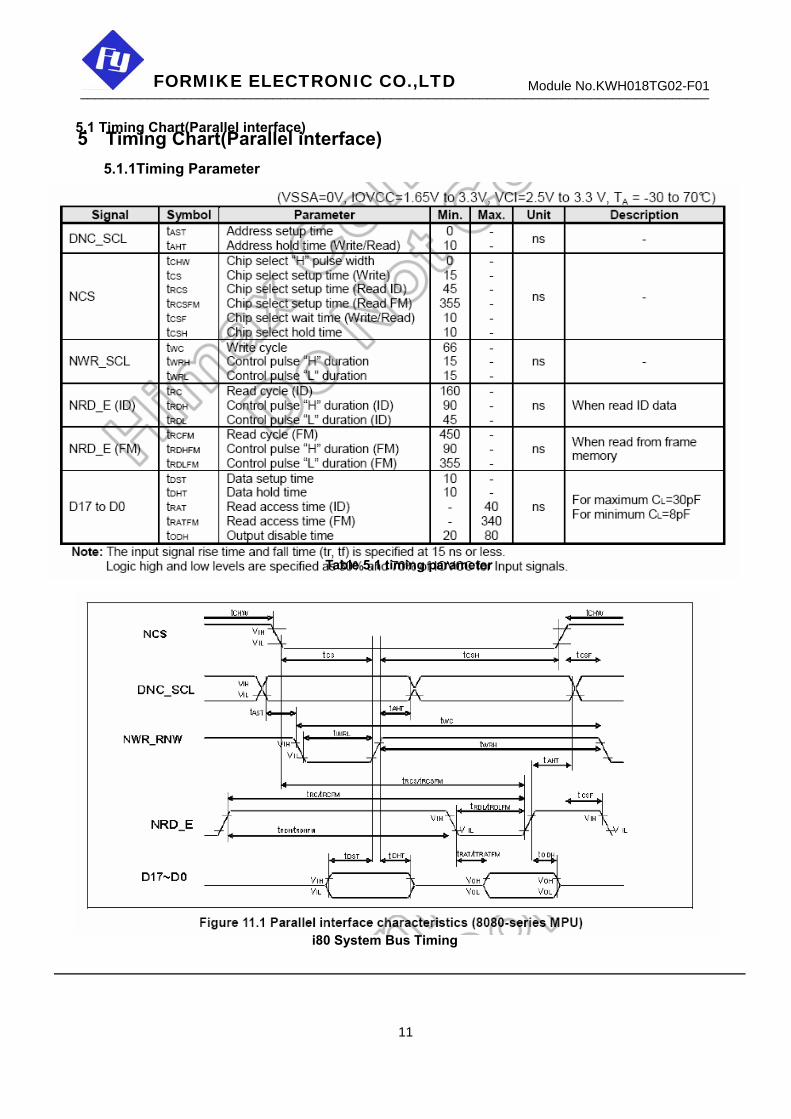
5.2.3 read function
8-bit read timing
17
Module No.KWH018TG02-F01FORMIKE ELECTRONIC CO.,LTD_____________________________________________________________________________________

5.3 Power On/Off sequence
5.3.1 Power on Sequence
Power Supply ON (VCI)
Power On Reset and Display OFF
Registers setting for power supply startup
Set the other registers
Display ON Sequence
Display ON
BLU ON
80ms or more Step-up circuit stabilizing time
Operational Amplifierstabilizing time
18
Module No.KWH018TG02-F01FORMIKE ELECTRONIC CO.,LTD_____________________________________________________________________________________

5.3.2 Power off Sequence
19
Module No.KWH018TG02-F01FORMIKE ELECTRONIC CO.,LTD_____________________________________________________________________________________

6 Optical Characteristics Ta=25
Item Symbol Condition Min Typ Max Unit RemarkθT 45 50 -
θB 15 20 -
θL 40 45 - View Angles
θR
CR 10≧
40 45 -
Degree Note 2
Contrast Ratio CR θ=0° 200 350 - - Note1 Note3
TON Response Time
TOFF 25 - 30 40 ms
Note1 Note4
x 0.222 0.272 0.322 White
y 0.255 0.305 0.355
x 0.540 0.590 0.640 Red
y 0.290 0.340 0.390
x 0.271 0.321 0.371 Green
y 0.461 0.511 0.561
x 0.096 0.146 0.196
Chromaticity
Blue y
Backlight is on
0.062 0.112 0.162
- Note5 Note1
Uniformity U - 70 80 - % Note1 Note6
NTSC - - - 40 - % Note 5
Luminance L 140 170 - cd/m2 Note1 Note7
Test Conditions:
1. VF=3.2V, IF=15mA(One LED current), the ambient temperature is 25 .
2. The test systems refer to Note 1 and Note 2.
20
Module No.KWH018TG02-F01FORMIKE ELECTRONIC CO.,LTD_____________________________________________________________________________________

Note 1: Definition of optical measurement system.
The optical characteristics should be measured in dark room. After 5 minutes operation, the
optical properties are measured at the center point of the LCD screen. All input terminals LCD
panel must be ground when measuring the center area of the panel.
Note 2: Definition of viewing angle range and measurement system. viewing angle is measured at the center point of the LCD by CONOSCOPE(ergo-80)。
Fig. 1 Definition of viewing angle
Item Photo detector Field Contrast
Ratio Luminance
ChromaticityLum
Uniformity
SR-3A 1°
Response Time BM-7A 2°
500mm
Photo detector
Field
LCD PanelTFT-LCD Module
The center of the screen
21
Module No.KWH018TG02-F01FORMIKE ELECTRONIC CO.,LTD_____________________________________________________________________________________

Note 3: Definition of contrast ratio
“White state “:The state is that the LCD should driven by Vwhite.
“Black state”: The state is that the LCD should driven by Vblack.
Vwhite: To be determined Vblack: To be determined.
Note 4: Definition of Response time The response time is defined as the LCD optical switching time interval between “White” state
and “Black” state. Rise time (TON) is the time between photo detector output intensity changed
from 90% to 10%. And fall time (TOFF) is the time between photo detector output intensity
changed from 10% to 90%.
Note 5: Definition of color chromaticity (CIE1931) Color coordinates measured at center point of LCD.
22
Module No.KWH018TG02-F01FORMIKE ELECTRONIC CO.,LTD_____________________________________________________________________________________

Note 6: Definition of Luminance Uniformity Active area is divided into 9 measuring areas (Refer Fig. 2). Every measuring point is placed at
the center of each measuring area.
Luminance Uniformity(U) = Lmin/ Lmax
L-------Active area length W----- Active area width
Fig. 2 Definition of uniformity
Lmax: The measured maximum luminance of all measurement position.
Lmin: The measured minimum luminance of all measurement position.
Note 7: Definition of Luminance : Measure the luminance of white state at center point.
23
Module No.KWH018TG02-F01FORMIKE ELECTRONIC CO.,LTD_____________________________________________________________________________________

7 Environmental / Reliability Test No Test Item Condition Remark
1 High Temperature Operation
Ts=+70, 240hrs Note1 IEC60068-2-1:2007,GB2423.2-2008
2 Low Temperature Operation Ta=-20, 240hrs IEC60068-2-1:2007
GB2423.1-2008
3 High Temperature Storage
Ta=+80, 240hrs IEC60068-2-1:2007 GB2423.2-2008
4 Low Temperature Storage Ta=-30, 240hrs IEC60068-2-1:2007
GB2423.1-2008
5
High Temperature & High Humidity Storage
Ta=+60, 90% RH 240 hours Note2 IEC60068-2-78 :2001 GB/T2423.3—2006
6 Thermal Shock (Non-operation)
-30 30 min~+70 30 min, Change time:5min, 20 Cycles
Start with cold temperature, End with high temperature, IEC60068-2-14:1984,GB2423.22-2002
7 Electro Static Discharge (Operation)
C=150pF, R=330Ω,5points/panelAir:± 8KV, 5times, Contact:± 4KV, 5 times, (Environment: 15~35, 30%~60%, 86Kpa~106Kpa)
IEC61000-4-2:2001 GB/T17626.2-2006
8 Vibration (Non-operation)
Frequency range:10~55Hz, Stroke:1.5mm Sweep:10Hz~55Hz~10Hz 2 hours for each direction of X.Y.Z. (6 hours for total)(Package condition)
IEC60068-2-6:1982 GB/T2423.10—1995
9 Shock (Non-operation)
60G 6ms, ± X,± Y,± Z 3times, for each direction
IEC60068-2-27:1987 GB/T2423.5—1995
10 Package Drop Test
Height:80 cm, 1 corner, 3 edges, 6 surfaces
IEC60068-2-32:1990 GB/T2423.8—1995
Note1: Ts is the temperature of panel’s surface.
Note2: Ta is the ambient temperature of sample.
24
Module No.KWH018TG02-F01FORMIKE ELECTRONIC CO.,LTD_____________________________________________________________________________________

8 Mechanical Drawing
FO
RM
IKE
EL
EC
TR
ON
IC C
O.,L
TD
KW
H0
18T
G02
-F0
1
Module No.KWH018TG02-F01FORMIKE ELECTRONIC CO.,LTD

9 Packing Information
No Item Model (Material) Dimensions(mm) Unit Weight(Kg) Quantity Remark
1 Module 34x47x2.4 TBD 672
2 Tray PET(Transmit) 315×247×10.3 TBD 48 Anti-static3 EPE EPE 315×247×5 0.0035 12
4 Anti-static bag PE 327×440 0.021 6
5 BOX Corrugated Paper 345×260×70 TBD 6
6 Desiccant Desiccant 45x50 0.0035 12
7 Carton Corrugated Paper 544×365×250 1.01 1
8 Total weight(Kg) TBD
KWH018TG02-F01
26
Module No.KWH018TG02-F01FORMIKE ELECTRONIC CO.,LTD_____________________________________________________________________________________

10 Precautions For Use of LCD Modules 10.1 Handling Precautions
10.1.1 The display panel is made of glass. Do not subject it to a mechanical shock by dropping it from a high place, etc.
10.1.2 If the display panel is damaged and the liquid crystal substance inside it leaks out, be sure not to get any in your mouth, if the substance comes into contact with your skin or clothes, promptly wash it off using soap and water.
10.1.3 Do not apply excessive force to the display surface or the adjoining areas since this may cause the color tone to vary.
10.1.4 The polarizer covering the display surface of the LCD module is soft and easily scratched. Handle this polarizer carefully.
10.1.5 If the display surface is contaminated, breathe on the surface and gently wipe it with a soft dry cloth. If still not completely clear, moisten cloth with one of the following solvents:
- Isopropyl alcohol
- Ethyl alcohol
Solvents other than those mentioned above may damage the polarizer. Especially, do not use the following:
- Water
- Ketone
- Aromatic solvents
10.1.6 Do not attempt to disassemble the LCD Module. 10.1.7 If the logic circuit power is off, do not apply the input signals. 10.1.8 To prevent destruction of the elements by static electricity, be careful to maintain an
optimum work environment. 10.1.8.1 Be sure to ground the body when handling the LCD Modules. 10.1.8.2 Tools required for assembly, such as soldering irons, must be properly ground. 10.1.8.3 To reduce the amount of static electricity generated, do not conduct assembly and
other work under dry conditions. 10.1.8.4 The LCD Module is coated with a film to protect the display surface. Be care when
peeling off this protective film since static electricity may be generated. 10.2 Storage precautions
10.2.1 When storing the LCD modules, avoid exposure to direct sunlight or to the light of fluorescent lamps.
10.2.2 The LCD modules should be stored under the storage temperature range. If the LCD modules will be stored for a long time, the recommend condition is:
Temperature : 0 ~ 40 Relatively humidity: ≤80%
10.2.3 The LCD modules should be stored in the room without acid, alkali and harmful gas. 10.3 Transportation Precautions
The LCD modules should be no falling and violent shocking during transportation, and also should avoid excessive press, water, damp and sunshine.
27