Embed Size (px)
Citation preview
FPGA Design Techniques I
FPGA Design Workshop

Objectives
After completing this module, you will be able to:
• Effectively use hierarchy• Describe the basic architecture of Xilinx FPGAs• Increase circuit reliability and performance by
applying synchronous design techniques
For Academic Use OnlyPresentation Name 2 For Academic Use Only
Outline
• Hierarchical Design• Overview of Xilinx FPGA
Architecture• Synchronous Design for Xilinx
FPGAs• Summary
For Academic Use OnlyPresentation Name 3 For Academic Use Only
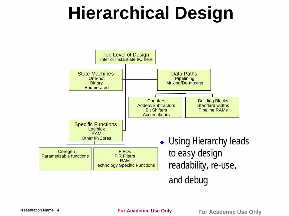
Hierarchical Design
Arithmetic
Using Hierarchy leads to easy design readability, re-use, and debug
State MachinesOne-hotBinary
Enumerated
CountersAdders/Subtractors
Bit ShiftersAccumulators
Building BlocksStandard widthsPipeline RAMs
Data PathsPipelining
Muxing/De-muxing
CoregenParametizable functions
FIFOsFIR Filters
RAMTechnology Specific Functions
Specific FunctionsLogiblox
RAMOther IP/Cores
Top Level of DesignInfer or instantiate I/O here
For Academic Use OnlyPresentation Name 4 For Academic Use Only
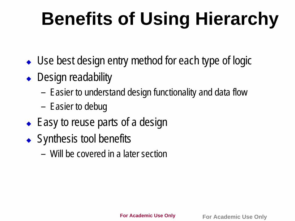
Benefits of Using Hierarchy
Use best design entry method for each type of logicDesign readability– Easier to understand design functionality and data flow– Easier to debug
Easy to reuse parts of a designSynthesis tool benefits– Will be covered in a later section
For Academic Use Only For Academic Use Only
Design Entry Methods
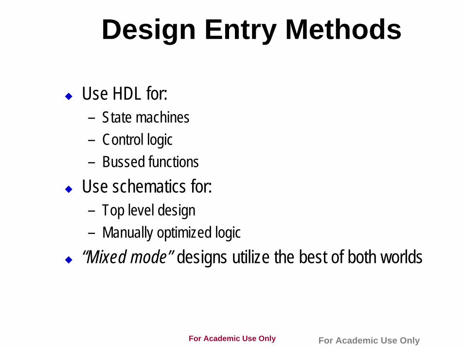
Use HDL for:– State machines– Control logic– Bussed functions
Use schematics for:– Top level design– Manually optimized logic
“Mixed mode” designs utilize the best of both worlds
For Academic Use Only For Academic Use Only
Design Readability
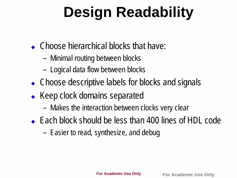
Choose hierarchical blocks that have:– Minimal routing between blocks– Logical data flow between blocks
Choose descriptive labels for blocks and signalsKeep clock domains separated– Makes the interaction between clocks very clear
Each block should be less than 400 lines of HDL code– Easier to read, synthesize, and debug
For Academic Use Only For Academic Use Only
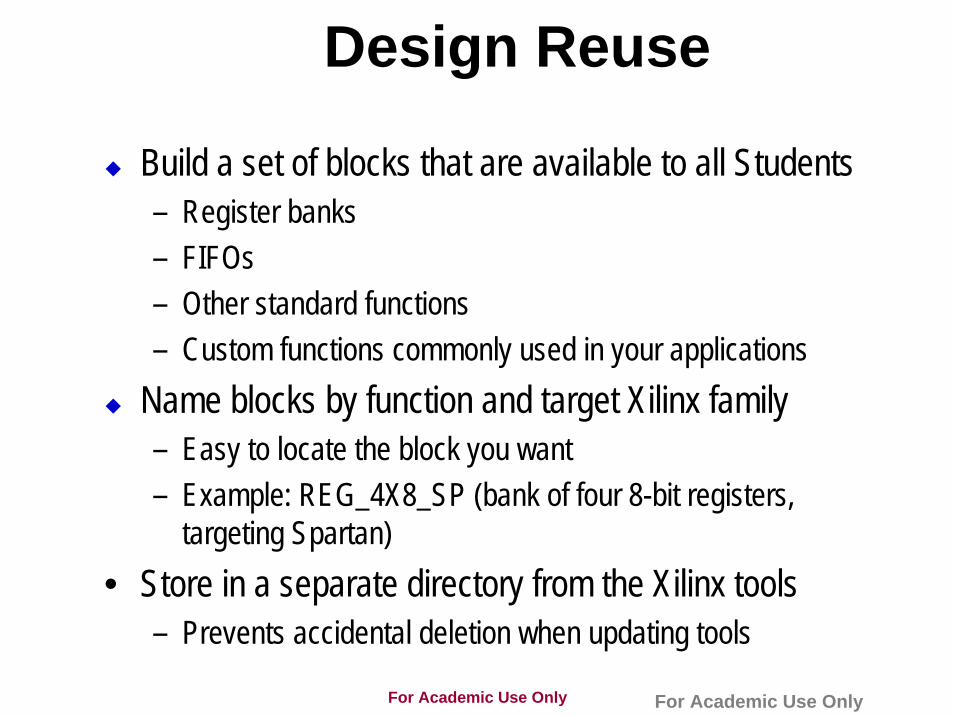
Design Reuse
Build a set of blocks that are available to all Students– Register banks– FIFOs– Other standard functions– Custom functions commonly used in your applications
Name blocks by function and target Xilinx family– Easy to locate the block you want– Example: REG_4X8_SP (bank of four 8-bit registers,
targeting Spartan)• Store in a separate directory from the Xilinx tools
– Prevents accidental deletion when updating tools
For Academic Use Only For Academic Use Only
Outline
Hierarchical DesignOverview of Xilinx ArchitectureSynchronous Design for Xilinx FPGAsSummary
For Academic Use OnlyPresentation Name 9 For Academic Use Only
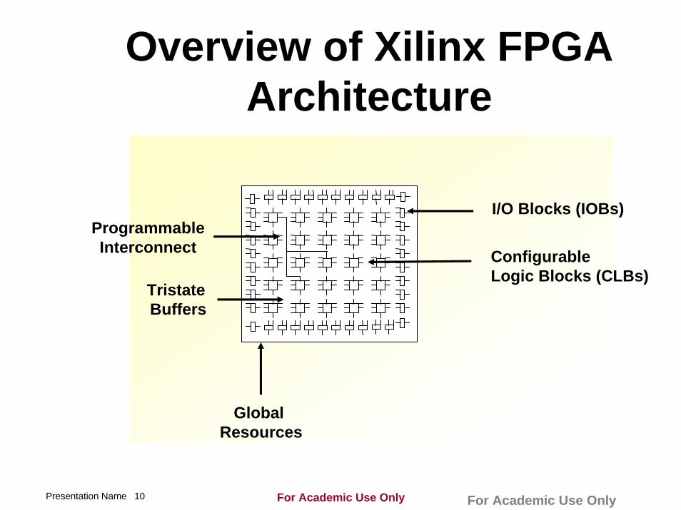
Overview of Xilinx FPGA Architecture
ProgrammableInterconnect
I/O Blocks (IOBs)
ConfigurableLogic Blocks (CLBs)
Tristate Buffers
Global Resources
For Academic Use OnlyPresentation Name 10 For Academic Use Only

CLB ResourcesBasic resource unit is the Logic Cell– 1 CLB contains 2 - 4 Logic Cells, depending on device family
Logic Cell = 4-input Look-Up Table (LUT) + D Flip-flop– LUT capacity limited by number of inputs, not complexity of function– LUTs can be used as ROM or synchronous RAM– Flip-flop can be configured as a transparent latch in Virtex and Spartan-II
LUT FF
For Academic Use OnlyPresentation Name 11 For Academic Use Only
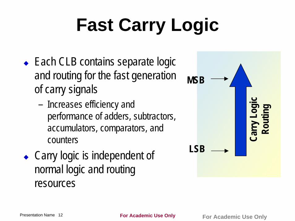
Fast Carry Logic
Each CLB contains separate logic and routing for the fast generation of carry signals– Increases efficiency and
performance of adders, subtractors, accumulators, comparators, and counters
Carry logic is independent of normal logic and routing resources
LSB
MSB
Carry
Log
icRo
utin
g
For Academic Use OnlyPresentation Name 12 For Academic Use Only
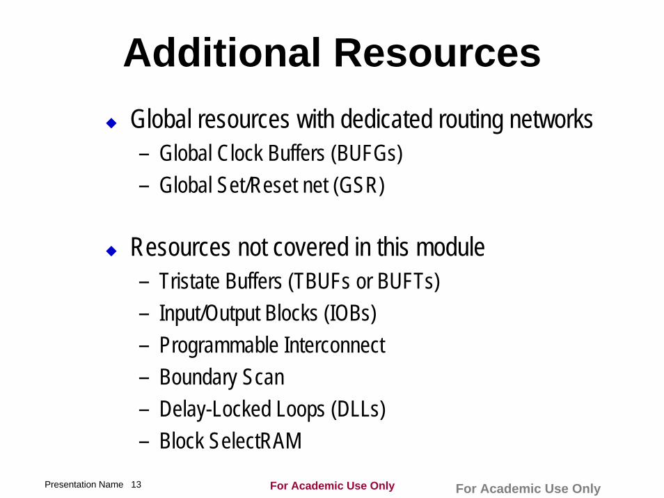
Additional ResourcesGlobal resources with dedicated routing networks– Global Clock Buffers (BUFGs)– Global Set/Reset net (GSR)
Resources not covered in this module– Tristate Buffers (TBUFs or BUFTs)– Input/Output Blocks (IOBs)– Programmable Interconnect– Boundary Scan– Delay-Locked Loops (DLLs)– Block SelectRAM
For Academic Use OnlyPresentation Name 13 For Academic Use Only
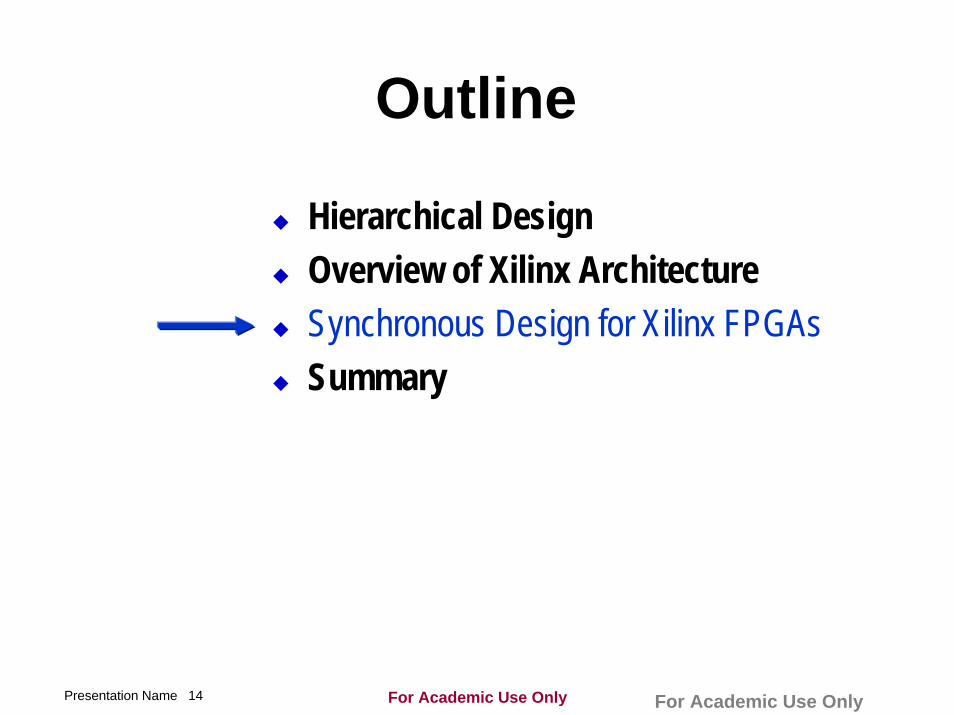
Outline
Hierarchical DesignOverview of Xilinx ArchitectureSynchronous Design for Xilinx FPGAsSummary
For Academic Use OnlyPresentation Name 14 For Academic Use Only
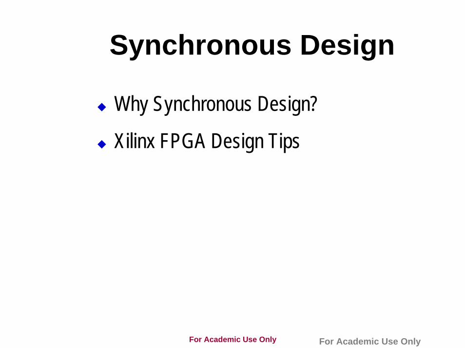
Synchronous Design
Why Synchronous Design?
Xilinx FPGA Design Tips
For Academic Use Only For Academic Use Only
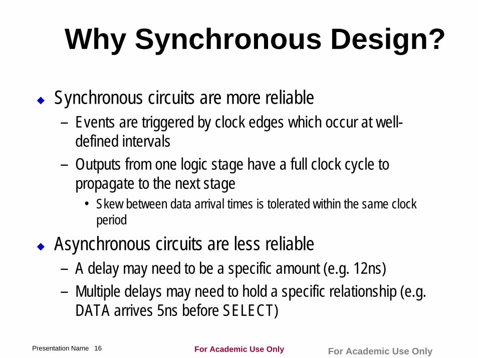
Why Synchronous Design?
Synchronous circuits are more reliable– Events are triggered by clock edges which occur at well-
defined intervals– Outputs from one logic stage have a full clock cycle to
propagate to the next stage• Skew between data arrival times is tolerated within the same clock
period
Asynchronous circuits are less reliable– A delay may need to be a specific amount (e.g. 12ns)– Multiple delays may need to hold a specific relationship (e.g.
DATA arrives 5ns before SELECT)
For Academic Use OnlyPresentation Name 16 For Academic Use Only
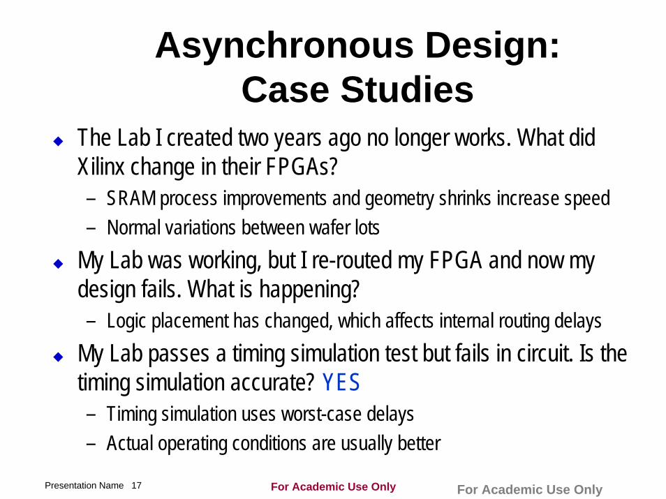
Asynchronous Design:Case Studies
The Lab I created two years ago no longer works. What did Xilinx change in their FPGAs?– SRAM process improvements and geometry shrinks increase speed– Normal variations between wafer lots
My Lab was working, but I re-routed my FPGA and now my design fails. What is happening?– Logic placement has changed, which affects internal routing delays
My Lab passes a timing simulation test but fails in circuit. Is the timing simulation accurate? YES– Timing simulation uses worst-case delays– Actual operating conditions are usually better
For Academic Use OnlyPresentation Name 17 For Academic Use Only
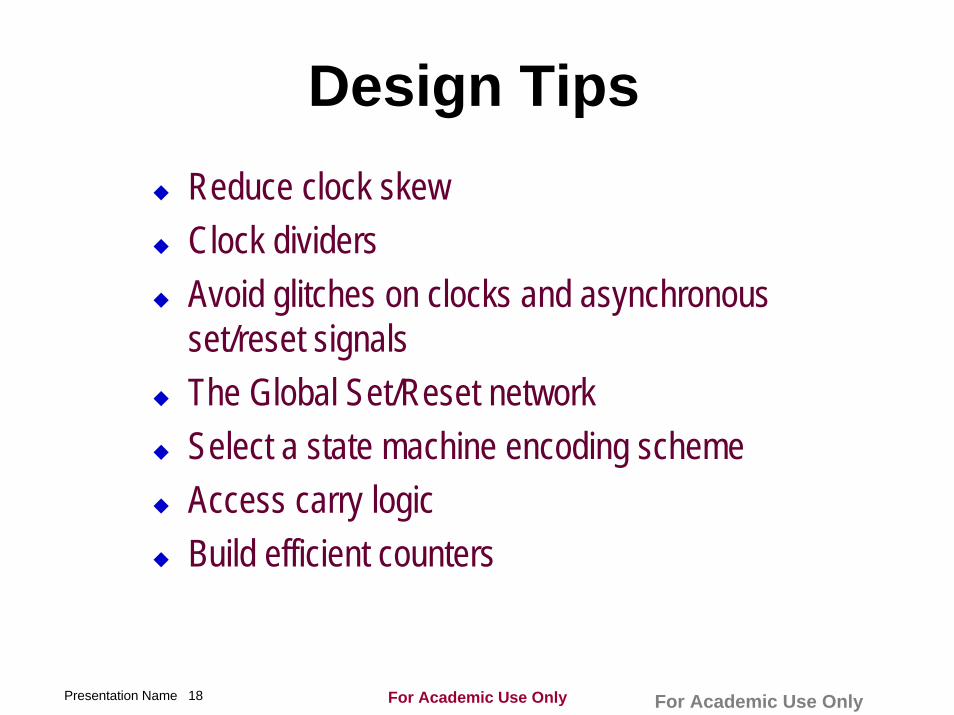
Design TipsReduce clock skewClock dividersAvoid glitches on clocks and asynchronous set/reset signalsThe Global Set/Reset networkSelect a state machine encoding schemeAccess carry logicBuild efficient counters
For Academic Use OnlyPresentation Name 18 For Academic Use Only

Clock SkewD Q_B Q_CINPUT
CLOCK
DD Q_A3.1
3.0
3.1 3.3
7.5 3.0A B C
• This shift register will not work because of clock skew!
Expected operation
Clock
Q_A
Q_B
Q_C
3 cycles
Clock skewed version
A & C Clock
Q_A
Q_B
Q_C
B Clock
2 cycles
For Academic Use OnlyPresentation Name 19 For Academic Use Only
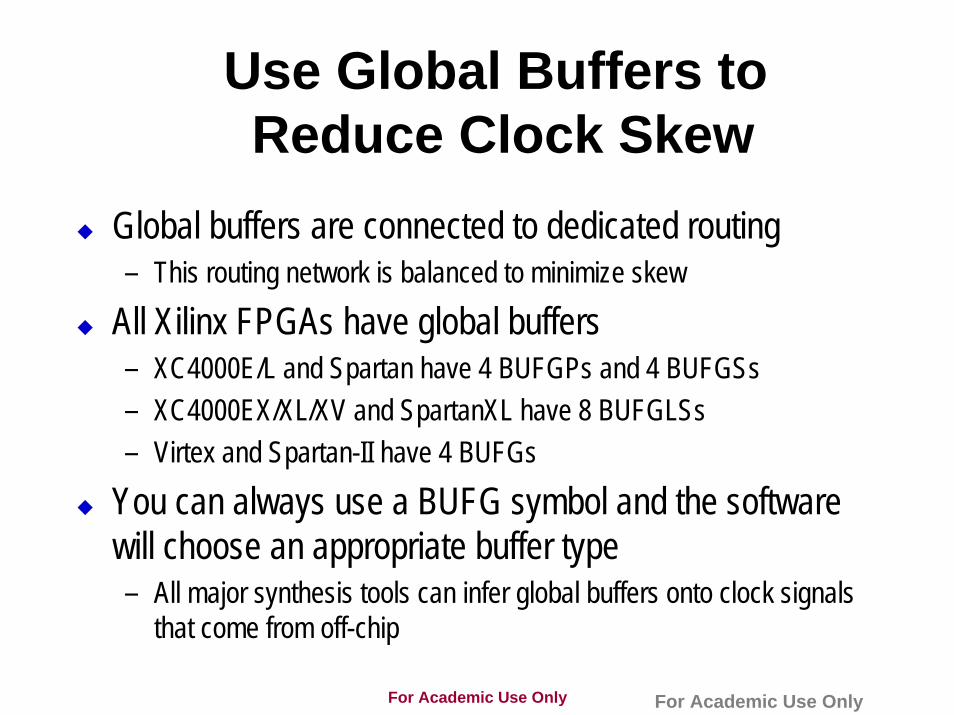
Use Global Buffers toReduce Clock Skew
Global buffers are connected to dedicated routing– This routing network is balanced to minimize skew
All Xilinx FPGAs have global buffers– XC4000E/L and Spartan have 4 BUFGPs and 4 BUFGSs– XC4000EX/XL/XV and SpartanXL have 8 BUFGLSs– Virtex and Spartan-II have 4 BUFGs
You can always use a BUFG symbol and the software will choose an appropriate buffer type– All major synthesis tools can infer global buffers onto clock signals
that come from off-chip
For Academic Use Only For Academic Use Only
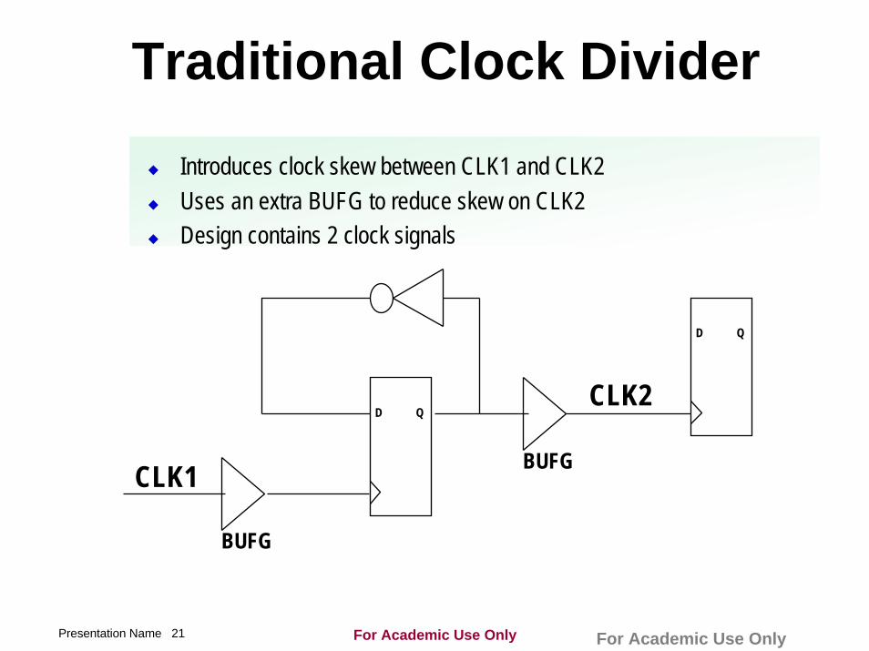
Traditional Clock Divider
Introduces clock skew between CLK1 and CLK2Uses an extra BUFG to reduce skew on CLK2Design contains 2 clock signals
D QCLK2
CLK1 BUFG
D Q
BUFG
For Academic Use OnlyPresentation Name 21 For Academic Use Only
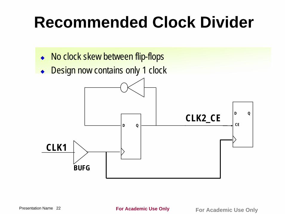
Recommended Clock Divider
No clock skew between flip-flopsDesign now contains only 1 clock
D QCLK2_CE
CLK1
D
CE
Q
BUFG
For Academic Use OnlyPresentation Name 22 For Academic Use Only
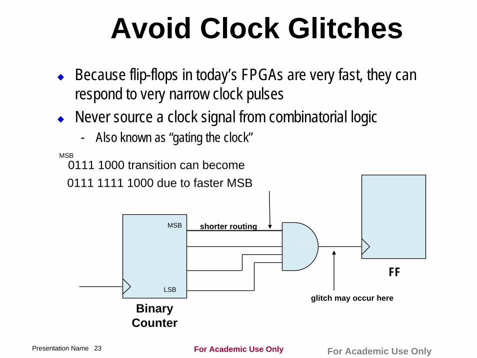
Avoid Clock GlitchesBecause flip-flops in today’s FPGAs are very fast, they can respond to very narrow clock pulsesNever source a clock signal from combinatorial logic- Also known as “gating the clock”
shorter routingMSB
0111 1000 transition can become0111 1111 1000 due to faster MSB
MSB
FFLSB
glitch may occur hereBinary
Counter
For Academic Use OnlyPresentation Name 23 For Academic Use Only
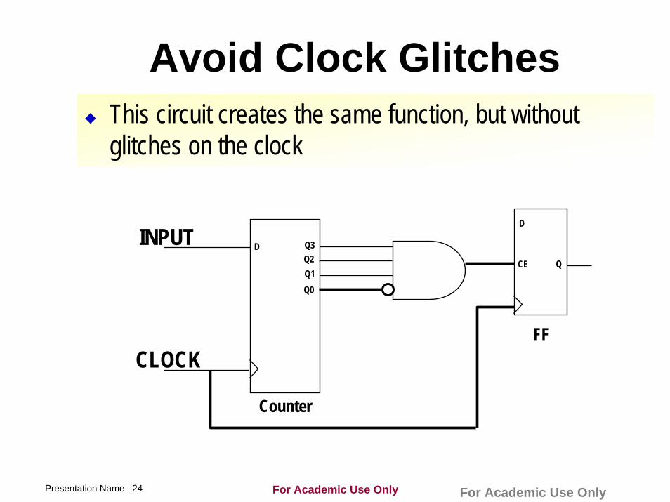
Avoid Clock GlitchesThis circuit creates the same function, but without glitches on the clock
D Q3INPUT
CLOCK
Counter
Q2Q1Q0
CE Q
D
FF
For Academic Use OnlyPresentation Name 24 For Academic Use Only
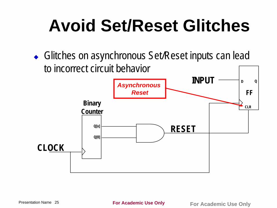
Avoid Set/Reset Glitches Glitches on asynchronous Set/Reset inputs can lead to incorrect circuit behavior
CLOCK
Q[x]
BinaryCounter
Q[0]
INPUT
RESET
Q
FFD
CLR
Asynchronous Reset
For Academic Use OnlyPresentation Name 25 For Academic Use Only
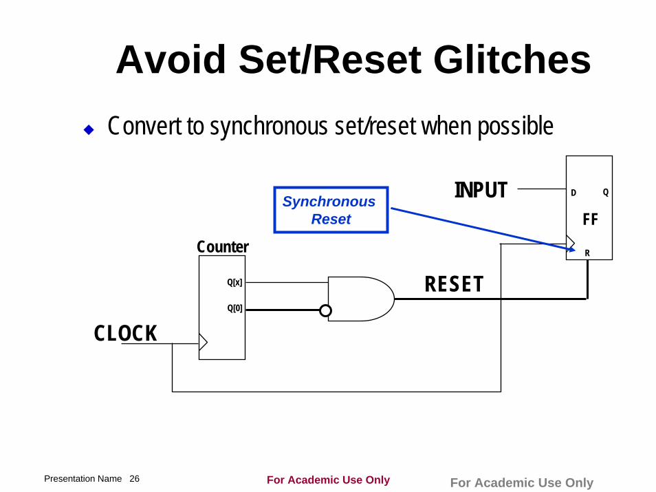
Avoid Set/Reset GlitchesConvert to synchronous set/reset when possible
For Academic Use OnlyPresentation Name 26 For Academic Use Only
CLOCK
Q[x]
Counter
Q[0]
RESET
INPUT Q
FFD
R
Synchronous Reset
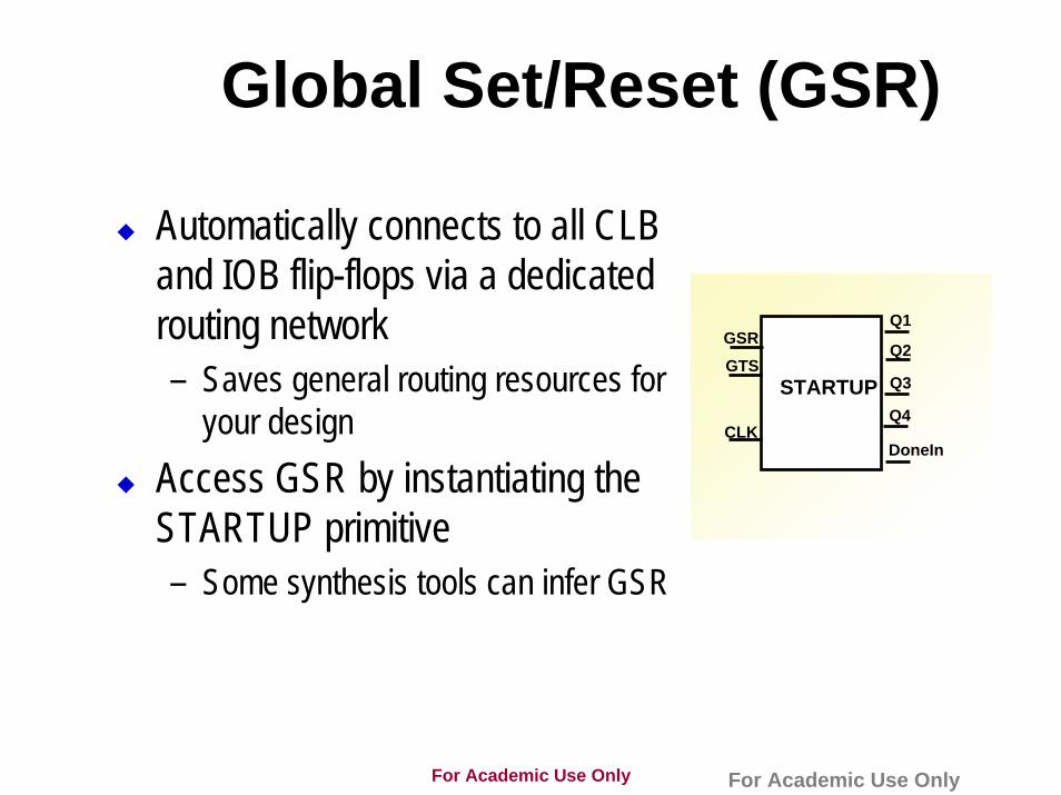
Global Set/Reset (GSR)
Automatically connects to all CLB and IOB flip-flops via a dedicated routing network– Saves general routing resources for
your designAccess GSR by instantiating the STARTUP primitive– Some synthesis tools can infer GSR
GSRGTS
CLK
Q1
Q2
Q3
DoneIn
STARTUPQ4
For Academic Use Only For Academic Use Only
Global Set/Reset
Use GSR when you have a chip-wide asynchronous reset signal and are targeting Spartan or XC4000 devices
Do not use GSR when you are targeting Virtex or Spartan-II– Plenty of general routing is available, and is faster than GSR
For Academic Use Only For Academic Use Only
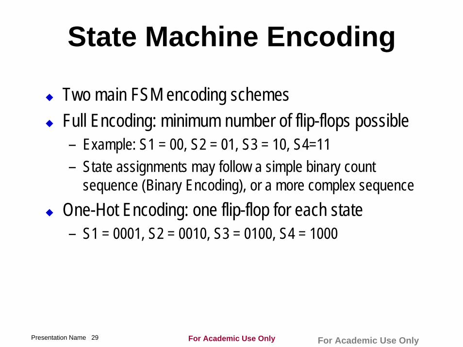
State Machine Encoding
Two main FSM encoding schemesFull Encoding: minimum number of flip-flops possible– Example: S1 = 00, S2 = 01, S3 = 10, S4=11– State assignments may follow a simple binary count
sequence (Binary Encoding), or a more complex sequenceOne-Hot Encoding: one flip-flop for each state – S1 = 0001, S2 = 0010, S3 = 0100, S4 = 1000
For Academic Use OnlyPresentation Name 29 For Academic Use Only
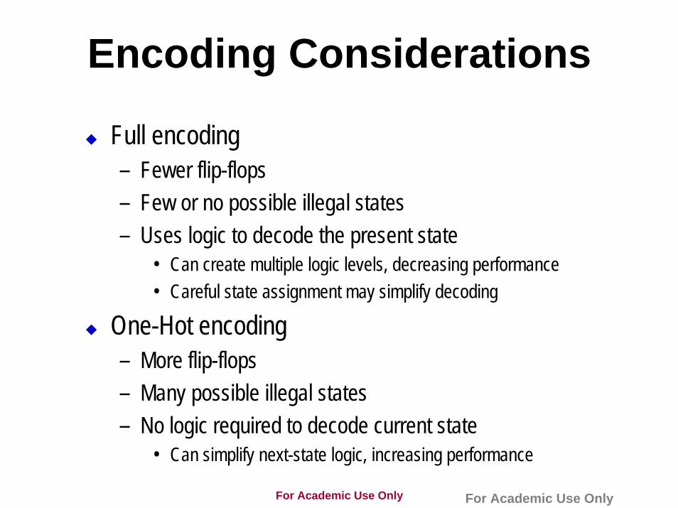
Encoding Considerations
Full encoding – Fewer flip-flops– Few or no possible illegal states– Uses logic to decode the present state
• Can create multiple logic levels, decreasing performance• Careful state assignment may simplify decoding
One-Hot encoding– More flip-flops– Many possible illegal states– No logic required to decode current state
• Can simplify next-state logic, increasing performance
For Academic Use Only For Academic Use Only
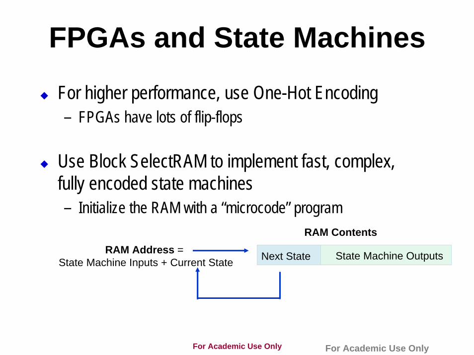
FPGAs and State Machines
For higher performance, use One-Hot Encoding– FPGAs have lots of flip-flops
Use Block SelectRAM to implement fast, complex, fully encoded state machines– Initialize the RAM with a “microcode” program
RAM Address = State Machine Inputs + Current State Next State State Machine Outputs
RAM Contents
For Academic Use Only For Academic Use Only
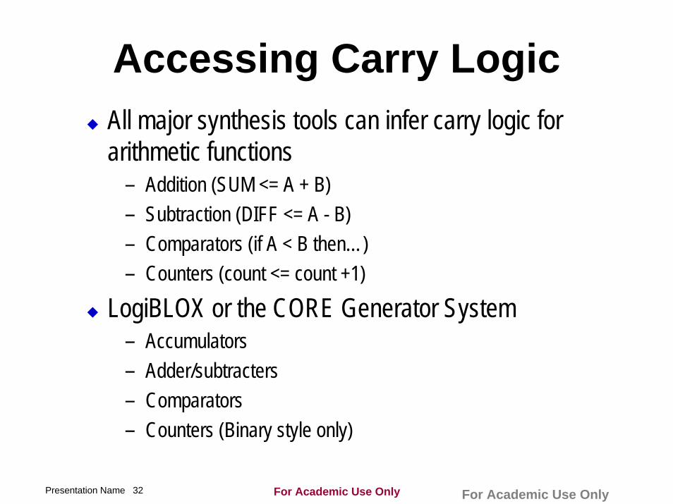
Accessing Carry LogicAll major synthesis tools can infer carry logic for arithmetic functions
– Addition (SUM <= A + B)– Subtraction (DIFF <= A - B)– Comparators (if A < B then…)– Counters (count <= count +1)
LogiBLOX or the CORE Generator System– Accumulators– Adder/subtracters– Comparators– Counters (Binary style only)
For Academic Use OnlyPresentation Name 32 For Academic Use Only
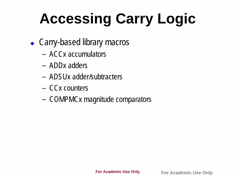
Accessing Carry LogicCarry-based library macros– ACCx accumulators– ADDx adders– ADSUx adder/subtracters– CCx counters– COMPMCx magnitude comparators
For Academic Use Only For Academic Use Only
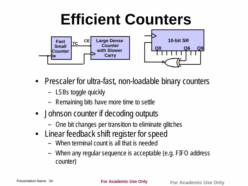
Efficient CountersLarge Dense
Counterwith Slower
Carry
TC CEFastSmall
Counter
10-bit SRQ0 Q9Q6
• Prescaler for ultra-fast, non-loadable binary counters– LSBs toggle quickly– Remaining bits have more time to settle
• Johnson counter if decoding outputs– One bit changes per transition to eliminate glitches
• Linear feedback shift register for speed– When terminal count is all that is needed– When any regular sequence is acceptable (e.g. FIFO address
counter)
For Academic Use OnlyPresentation Name 34 For Academic Use Only
Outline
Hierarchical DesignOverview of Xilinx ArchitectureSynchronous Design for Xilinx FPGAsSummary
For Academic Use OnlyPresentation Name 35 For Academic Use Only
SummaryProper use of hierarchy aids design readability and debugSynchronous designs are more reliable than asynchronous designsFPGA design tips– Global clock buffers eliminate skew– Avoid glitches on clocks and asynchronous set/resets– FSM encoding scheme can affect design performance– Increase performance of arithmetic functions by using carry
logic– Consider different counter styles to meet your design needs
For Academic Use Only For Academic Use Only