Embed Size (px)
Citation preview

FPGA prototyping of large reconfigurable ADPLL
network for distributed clock generation
Chuan Shan, Eldar Zianbetov, Weiqiang Yu, Francois Anceau, Olivier
Billoint, Dimitri Galayko
To cite this version:
Chuan Shan, Eldar Zianbetov, Weiqiang Yu, Francois Anceau, Olivier Billoint, et al.. FPGAprototyping of large reconfigurable ADPLL network for distributed clock generation. Recon-figurable Computing and FPGAs (ReConFig), 2013 International Conference on, Dec 2013,Cancun, Mexico. pp.1 - 6, 2013, <10.1109/ReConFig.2013.6732295>. <hal-01053762>
HAL Id: hal-01053762
http://hal.upmc.fr/hal-01053762
Submitted on 4 Aug 2014
HAL is a multi-disciplinary open accessarchive for the deposit and dissemination of sci-entific research documents, whether they are pub-lished or not. The documents may come fromteaching and research institutions in France orabroad, or from public or private research centers.
L’archive ouverte pluridisciplinaire HAL, estdestinee au depot et a la diffusion de documentsscientifiques de niveau recherche, publies ou non,emanant des etablissements d’enseignement et derecherche francais ou etrangers, des laboratoirespublics ou prives.
FPGA Prototyping of Large Reconfigurable ADPLL
Network for Distributed Clock Generation
Chuan Shan 1, Eldar Zianbetov 1, Weiqiang Yu 1, Francois Anceau 1, Olivier Billoint 2, Dimitri Galayko 1
1 Laboratoire d’informatique de Paris 6 (LIP6)
University of Pierre and Marie Curie (UPMC), Paris, France2 CEA-LETI, Grenoble, France
Email: 1{First name.Last name}@lip6.fr, 2{First name.Last name}cea.fr Tel: +33 (0)1 44 27 70 16
Abstract—In this paper, we present an FPGA platform forthe design and study of a network of coupled all-digital phaselocked loops (ADPLLs). An implementation of a programmableand reconfigurable 10× 10 ADPLL network is described, whichis designed for prototyping distributed clock generation in largesynchronous system on chip (SoC). The paper emphasizes thereconfigurability of proposed system, which allows exploitingstability issues and nonlinear behavior of a N ×M network ofcoupled oscillators (the dimension can be configured from 1×1 to10×10). Configurations with different parameters are comparedand analyzed. A dynamic setup mechanism is proposed, allowingselecting the desired synchronized state. Experimental resultsvalidate theoretical analysis about circuit parameters and demon-strate the global synchronization of network and performance fordifferent configurations.
Keywords-Synchronization, ADPLL, FPGA, prototyping, re-configurability.
I. INTRODUCTION
Clocking is essential for large system on chip (SoC) like
multi-core processors. The main clock related issue is the
difficulty of implementing a global centralized clock distri-
bution in advanced deep submicron CMOS technologies. For
this reason, nowadays large SoCs are partitioned into several
small synchronous clocking areas (clock domains), and the
communication between the logic blocks in different clock do-
mains is asynchronous (Globally Asynchronous Locally Syn-
chronous architecture). This solution presents several draw-
backs, particularly in what concerns chip design, verification
and by consequence, system reliability. A fully-synchronous
design requires a synchronization between the local clocks.
For this, instead of using a centralized clock distribution, our
study explores an alternative technique of distributed clock
generation: a network of coupled and synchronized oscillators
for the generation of local clocks of the synchronous clocking
areas (SCA). If the clock generators of each clock domain are
synchronized in phase and in frequency, synchronous com-
munications are possible between the zones. In our study, the
synchronization between the oscillators is achieved through the
network of coupled all-digital phase locked loops (ADPLL).
The advantage of this solution is a use of only local links
between the oscillators, and exploitation of the smartness of
digital circuits for management of oscillator synchronization,
comparing with previous analog implementations [1].
The main challenge in implementation of this solution is
the design of a large size coupled ADPLL network: this is
a multidimensional nonlinear digital system, whose stability
and performance must be controlled by digital correctors
embedded in the network nodes. This nonlinear system has
many degrees of freedom, and by consequence, it has multiple
steady operation modes depending on system coefficients and
initial conditions. To study these issues, we need a prototype
to model as precisely as possible the behavior of an ASIC-
based ADPLL network. Because of digital implementation of
the system, the FPGA prototyping appears to be an appropriate
solution.
This work presents an FPGA implementation of 10×10 net-
work of coupled oscillators, which is a prototype for a chip in
65nm CMOS technology whose design is ongoing. The FPGA
model of the ADPLL network has the same architecture and
the same parameter values as the future CMOS ASIC circuit,
however, scaled down proportionally in frequency because of
the maximum frequency limit of the FPGA platform. The
analog/digital blocks of the ADPLL (the digitally controlled
oscillator and the phase-frequency detector) have a particular
implementation adapted to the FPGA limitations.
In section II the architecture of the 10 × 10 network and
its functional blocks are described. The procedure allowing
homothetic sizing of FPGA prototype with respect to the ASIC
prototype is also presented in this section. Section III discusses
about how we use the system reconfigurability feature to
verify the relation between different parameters and system
performance, and how to avoid undesired steady states. Section
IV presents experimental results to validate our theoretical
analysis.
II. NETWORK ARCHITECTURE
The topology of the 10×10 network is presented in Fig. 1.
It is composed of 100 filter/oscillator (FO) blocks and one
phase frequency detector (PFD) between each two neighboring
synchronous clock areas (SCA) for measuring the phase error
between each coupled oscillators (180 PFDs). The PFD placed
in the upper-left corner compares the phase of the oscillator
clock in SCA1-1 with the input reference clock. Such a
network, if properly designed, is synchronized: it means that
the all oscillators have the same frequency and phase as
FO
PFD
FO
PFD
FO
PFD
PFD
FO
PFD
FO
PFD
FO
PFD
PFD PFD
PFD PFD PFD
FO
PFD
FO
PFD
FO
PFD
PFD PFD PFD
+
SCA1-1 SCA1-2 SCA1-3
SCA2-1 SCA2-2 SCA2-3
SCA3-1 SCA3-2 SCA3-3
+
Referenceclock
PFD
PFD
FO
PFD
FO
PFD
FO
PFD
PFD
PFD FO
PFD
SCA1-10
SCA2-10
SCA3-10
PFD
FO
PFD
FO
PFD
FO
PFD
PFD PFD
SCA10-1 SCA10-2 SCA10-3
PFD
FO
PFD
SCA10-10
Fclk(1,1) PFD
Fref
Fclk(2,1)
Fclk(2,1)
Fclk(3,1)
Fclk(2,1)
Fig. 1: 10× 10 network of coupled PLL
the input reference signal, and residual synchronization phase
errors are small and limited in a well-defined range.
The structure of a network node is presented in Fig. 2 [2].
Each node contains 2, 3 or 4 PFDs: each PFD detects
the phase/frequency difference between the locally-generated
clock and a neighboring clock. The number of PFDs depends
on the position of node. A PFD generates a 5-bit signed binary
code. For each node, the errors with neighbors are added and
processed by the loop filter (LF), so as to generate a 10-bit
control word for the digitally controlled oscillator (DCO). The
loop filter is a Proportional-Integral (PI) filter.
CLKi,j
Local oscillator
Loopfilter
Errorcombiner
Nodei,jDistributed PLL
CLK i,j-1
PFD
CLK i+1,jCLK i-1,j
CLK i,j+1
Divider
/N
Total error
Local high freq. clockLocal divided clock
clo
ck t
o c
ircu
itry
PFD PFD
PFD
Fig. 2: Architecture of ADPLL
A. PFD
Fig. 3 presents the structure of the PFD. The Bang-Bang
Phase-Frequency Detector (BB-PFD) detects the sign of the
phase error (SIGN ) and the interval of it (MODE) [3].
The duration of the signal MODE represents the absolute
value of the phase error. It is applied to the input of TDC,
which converts the duration of input signal to an unsigned
binary code (Dout), which is then combined with the SIGN
signal by the arithmetic block to form a signed binary code
(ERROR). The transfer function is presented in Fig. 4.
BB-PFD
TDC
Arithmetic
block
SIGN MODE
ERROR
ref
div
DoutAbsolute phase
error
Fig. 3: Architecture of PFD
The BBPFD can be seen as a finite state automaton driven
by events (rising edges) at its inputs. Inspired by [3], it is
implemented similarly in ASIC and FPGA platforms.
In the ASIC-based TDC, the duration of the signal MODE
is quantified by a tapped delay line [4]. The sensitivity of PFD
(∆TASICTDC ) is defined as one stage delay in the delay line.
Since a logic gate with a wanted delay cannot be realized in
FPGA, the TDC is implemented as a digital chronometer with
an external clock, counting the number of the clock events
included in the measured time interval. The period of the ex-
ternal clock corresponds to the sensitivity of PFD (∆TFPGATDC ).
However, the external clock is not always synchronized with
the beginning of the time interval to measure. Hence, even
if the time interval is below the TDC time step and if the
clock event happens to be inside the interval, the FPGA-based
TDC may output 1, whereas the ASIC-based TDC outputs 0.
It causes a signal-correlated fluctuation with amplitude of ±1
unit over the output code, and the sign of the fluctuation is
the same as the sign of the error.
Fig. 4: Transfer function of PFD
B. Loop filter
The PI filter is implemented as the loop filter. Its transfer
function is the following:
H(z) =(
Kp +Ki
1− z−1
)
z−2 (1)
where Kp and Ki are programmable gain coefficients of
the proportional and integral paths respectively. The multi-
plier z−2 models the two cycles delay introduced by the
two registers in the loop filter. Theoretical investigations [5]
[6] provide the following specification for the coefficients:
Kp ∈ {1...0.03},Ki ∈ {1...0.00024}. The calculation inside
the filter is achieved in fixed point arithmetic. The coefficients
Kp and Ki are represented as a ratio of a programmable
integer number and a power of 2 integer number:
Kp =K1
25, Ki =
K2
212(2)
where K1 is integer in the range (0...31), and K2 is in the
range (0...212 − 1). A constant offset 512 is added to the sum
of proportional and integral values to shift the start-up value
from zero to the middle of the range, which reduces the worse
case frequency acquisition time by half.
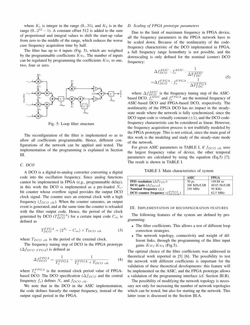
The filter has up to 4 inputs (Fig. 5), which are weighted
by the programmable coefficients Kwi. The number of inputs
can be regulated by programming the coefficients Kwi to one,
two, four or zero.
12
5
21 21
14 9
9
1/25
1/212
10
K1
K2
to D
CO
5128
9
7
7
Kw1
Kw2
Kw3
Kw4
15
2
3
4
5
2
2
75
2
8
75
2
from
PF
D
clk
Z-1
clk
Z-1div
div
clk
Z-1
div
Fig. 5: Loop filter structure
The reconfiguration of the filter is implemented so as to
allow all coefficients programmable. Hence, different con-
figurations of the network can be applied and tested. The
implementation of the programming is explained in Section
III.
C. DCO
A DCO is a digital-to-analog converter converting a digital
code into the oscillation frequency. Since analog functions
cannot be implemented in FPGA (e.g., programmable delay),
in this work the DCO is implemented as a pre-loaded Nc-
bit counter whose overflow signal provides the output DCO
clock signal. The counter uses an external clock with a high
frequency (fDCO clk). When the counter saturates, an output
event is generated, and at the same time the counter is reloaded
with the filter output code. Hence, the period of the clock
generated by DCO (TFPGADCO ) for a certain input code Cin is
defined as
TFPGADCO = (2Nc − Cin)× TDCO clk (3)
where TDCO clk is the period of the external clock.
The frequency tuning step of DCO in the FPGA prototype
(∆fDCO FPGA) is defined as
∆fFPGADCO =
1
TFPGAo
−1
TFPGAo + TDCO clk
(4)
where TFPGAo is the nominal clock period value of FPGA-
based DCO. The DCO specification (∆fDCO and the central
frequency fo) defines Nc and fDCO clk.
We note that in the DCO in the ASIC implementation,
the code defines linearly the output frequency, instead of the
output signal period in the FPGA.
D. Scaling of FPGA prototype parameters
Due to the limit of maximum frequency in FPGA device,
all the frequency parameters in the FPGA network have to
be scaled down. Because of the nonlinearity of the code-
frequency characteristic of the DCO implemented in FPGA,
a full frequency range homothety is not possible, and the
downscaling is only defined for the nominal (center) DCO
frequency:
∆fASICDCO : fASIC
o :1
∆TASICTDC
=∆fFPGADCO : fFPGA
o :1
∆TFPGATDC
(5)
where ∆fASICDCO is the frequency tuning step of the ASIC-
based DCO. fASICo and fFPGA
o are the nominal frequency of
ASIC-based DCO and FPGA-based DCO, respectively. The
nonlinearity of the FPGA DCO has no impact in the steady-
state mode where the network is fully synchronized, since the
DCO input code is virtually constant (±1), and the DCO code-
frequency characteristic can be considered as linear. However,
the frequency acquisition process is not truthfully modeled by
the FPGA prototype. This is not critical, since the main goal of
this work is the modeling and study of the steady-state mode
of the network.
For given ASIC parameters in TABLE I, if fDCO clk uses
the largest frequency value of device, the other temporal
parameters are calculated by using the equation (Eq.5) [7].
The result is shown in TABLE I.
TABLE I: Main characteristics of system
ASIC FPGA
PFD resolution (∆TTDC ) 30 ps 149.88 nsDCO gain (∆fDCO) 200 KHz/LSB 40.03 Hz/LSBNominal frequency (fo) 250 MHz 50 KHz
DCO counter frequency (fFPGA
DCOclk) 62.5 MHz
III. IMPLEMENTATION OF RECONFIGURATION FEATURES
The following features of the system are defined by pro-
gramming:
• The filter coefficients. This allows a test of different loop
correction strategies.
• The network topology, connectivity and weight of dif-
ferent links, through the programming of the filter input
gains Kw1-Kw4 (Fig.5).
The optimal choice of the filter coefficients was addressed in
theoretical work reported in [5] [6]. The possibility to test
the network with different coefficients is important for the
validation of these theoretical developments: this feature will
be implemented on the ASIC, and the FPGA prototype allows
a validation of the programming interface (cf. Section III.B).
The possibility of modifying the network topology is neces-
sary not only for increasing the number of network topologies
which can be tested, but also for starting up the network. This
latter issue is discussed in the Section III.A.

A. Reconfiguration for the selection of the desired steady
states
The circuit in Fig. 2 minimizes the signal ”Total error”,
which is the sum of the phase errors of the local node with
its neighbors. However, due to the cyclic (modular) nature of
phase and a large number of freedom degrees in the complex
system, there is a possibility to have this signal zero (actually,
n× 2π) whereas the individual errors are not zero. Moreover,
such state can be a steady-state, in which the oscillators are
synchronized in frequency but keeping fixed large phase errors
(e.g., as shown in Fig. 6 captured by oscilloscope). Obviously,
for the clock synchronization applications, such a mode is not
desirable, since the phase error between the oscillators must
be minimized. The problem of this architecture is its incapa-
bility of distinguishing the desired mode with all zero phase
errors from undesired modes sometimes called modelocks. The
steady state to which the system settles depends on its initial
condition, which can be considered as random in a real system.
Hence, the network designer should add a mechanism allowing
a selection of the desired mode.
Many solutions have been proposed for this problem [1] [8].
The solution we propose is based on an artificial determination
of network initial conditions from which the system settles
to the desired mode. This method makes use of the network
reconfigurability. The idea is to force the system to run towards
the desired steady state at the start-up of system, and when the
network operates near the desired steady state, the autonomy
is given back to the system and the system settles down to the
state at which all phase errors are zero.
Fig. 6: One clock in network and its neighboring clocks:
Undesired steady state
It has been proven that the modelocks are only possible
in the PLL networks having phase error propagation loops.
By consequence, unidirectional networks do not suffer from
the modelock issues [1]. However, an unidirectinoal network
configuration is not suitable for the oscillator synchronization,
since the phase error accumulates through the network, and
is amplified by the unidirecitonal PLL chains. However, the
phase error provided by unidirectional configuration is small
enough to determine an initial state, from which the bidirec-
tional network can settle to the desired mode. In this way, the
start-up of the network is as follows:
• The network parameters Kwi are programmed so as to
set the network into unidirectional configuration,
• After the settlement of the system, Kwi are re-
programmed so as to set the network into the bidirectional
configuration.
The switching of the connectivity is implemented by pro-
gramming dynamically the coefficients Kwi in the loop filters
presented in Fig. 5.
The main challenge of this solution on large ADPLL
network is the accumulation of the phase errors in the unidi-
rectional mode: the clock generated by the nodes far from the
reference (source) point has a relatively poor quality compared
with clocks near the reference. By consequence, it gives a poor
definition of the initial state for the bidirectional mode. For this
reason, the unidirectional topology should be chosen to reduce
the maximal distance of the error propagation.
Two topology of 4×4 unidirectional networks are presented
in Fig. 7. To compare them, we introduce a parameter D
standing for the phase error propagation distance between
two clock domains, which is equal to the number of clock
domain borders that the information passes through from one
node to the other. Criteria of choosing the best unidirectional
configuration is that the parameter D from the node at the
upper-left corner (with coordinates (1, 1)) to each node in
the network should be as small as possible. The topology
in Fig. 7(a) uses a zigzag chain to connect all the nodes
together. In this way, the value of D increases linearly as
the geometry gets larger. In a 4 × 4 network, the distance
between the last node at the end of the chain and the upper-
left (which receives the reference clock) node is 15, while
in a 10 × 10 network, the value is 99. Fig. 7(b) shows a
network with a comb topology. In this case, the distance D
between each node and the upper-left node is the Manhattan
distance. The Manhattan distance between a node X=(X1, X2)
and a node Y=(Y1, Y2) is defined as: |x1 − x2| + |y1 − y2|,which is the shortest distance between two intersections in a
grid. In a 4 × 4 network, the longest distance is 6, which is
between the upper-left node and the lower-right node. For a
10× 10 network using this configuration, the longest distance
is 18. Both configuration topologies have been implemented
in FPGA and tested. The experimental results are presented in
Section IV.
ref(1, 1) (1, 2) (1, 3) (1, 4)
(2, 1) (2, 2) (2, 3) (2, 4)
(4, 1) (4, 2) (4, 3) (4, 4)
(3, 1) (3, 2) (3, 3) (3, 4)
ref(1, 1) (1, 2) (1, 3) (1, 4)
(2, 1) (2, 2) (2, 3) (2, 4)
(4, 1) (4, 2) (4, 3) (4, 4)
(3, 1) (3, 2) (3, 3) (3, 4)
(a) (b) Fig. 7: Unidirectional mode topology: (a) type 1 - zigzag; (b)
type 2 - comb (the arrows show the connection in the network
and the error propagation direction)
B. Programming and reconfiguration of the network
In order to implement the dynamic two-step start-up tech-
nique presented above, the programming interface should
allow an on-the-fly reconfiguration of the network without
suspending, which requires a simultaneous (synchronous) re-
programming of all parameters in one ADPLL. Since the
number of bits to be programmed is large (25 bits per node), a
serial interface with two-stage parallel buffers is used for the
programming sequence transmission.
SCK
SDAi
UPD
N
Serial In Parallel Out
register
Serial data in
Parallel data out
SDAi+1SCKXI1
Parallel data out
Parallel data inParallel In
Parallel Out register
coefficients to local signal
processing block
to following SPI blocks
XI0
XI2
0 1
Kp KiKw1Kw2Kw3Kw4
242 3 4 5 6 7 8 1213
Data sequence for one signal processing block
from previous SPI blocks
Fig. 8: Schematic of the serial programming interface (SPI)
The designed serial programming interface (SPI) in Fig. 8
is composed of a two-stage buffer (registers XI0 and XI2)
and one flip-flop (XI1). The register XI0 is a serial-to-parallel
converting register which shifts in the input series data on
SDAi and generates a parallel word at its outputs parallel data
out. The actual values of the outputs of XI0 represent the bits
to be programmed. However, during the read-in process, the
parallel data out outputs have transient meaningless values.
For this reason, the outputs of this register are not applied
directly to the node block, but to the storage parallel register
XI2. This loading is ordered by a global UPD signal. When
all programming bits are sent, the UPD signal goes high. Ide-
ally, all the network starts operating with updated parameters at
the rising edge of UPD. In practice, there are skews between
signal UPD arriving time at nodes in different positions of the
network because of transmission delay. The maximum skew
should be less than one reference clock cycle, while it is not
a constraint for this low frequency FPGA prototype.
The programming interface is easily extendable by cascad-
ing (Fig. 9). The programming interfaces of two blocks are
joined by connecting the last output bit of the register XI0 of
one block to the SDAi of the another block. The two blocks
share the same UPD and SCK signals. In this way, for any
length of the programming sequence, the interface requires
only three external pads: SCK, SDA and UDP (clock, data
and load signals).
IV. EXPERIMENTAL RESULTS
An FPGA emulator for a network with 100 clock generators
is implemented on ALTERA CYCLONE II EP2C70 platform.
A. Effect of dynamic configuration on undesired stable state
prevention
Fig. 10 demonstrates the clock signals of the main network
diagonal nodes, when the network is configured in unidirec-
tional mode. As explained in Section III.A, the phase error
UPD
SDAi-1
SDA in
Parallel data out
SDAiSCK
coefficients to local signal
processing blocks
SPI
SDA out
SCK
UPD
SDA in
Parallel data out
SDA out
SCK
UPD
i-1 SPIi
SDA in
Parallel data out
SDA out
SCK
UPD
SPIi+1
SDAi+1 SDAi+2
Fig. 9: Cascading the programming interfaces of several blocks
between CLK10-10 (clock generated at SCA10-10 in Fig. 1)
and the reference clock REF is smaller with comb shaped
configuration compared with the zigzag type.
Fig. 10: Clocks in unidirectional mode at steady state: (a) type
1 - zigzag; (b) type 2 - comb
For this reason, the comb shaped topology is chosen for
unidirectional mode as the first phase of the dynamic configu-
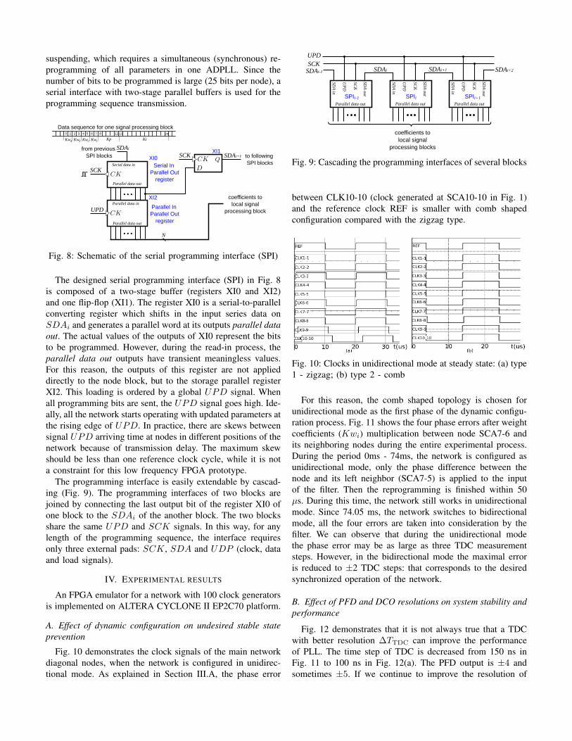
ration process. Fig. 11 shows the four phase errors after weight
coefficients (Kwi) multiplication between node SCA7-6 and
its neighboring nodes during the entire experimental process.
During the period 0ms - 74ms, the network is configured as
unidirectional mode, only the phase difference between the
node and its left neighbor (SCA7-5) is applied to the input
of the filter. Then the reprogramming is finished within 50
µs. During this time, the network still works in unidirectional
mode. Since 74.05 ms, the network switches to bidirectional
mode, all the four errors are taken into consideration by the
filter. We can observe that during the unidirectional mode
the phase error may be as large as three TDC measurement
steps. However, in the bidirectional mode the maximal error
is reduced to ±2 TDC steps: that corresponds to the desired
synchronized operation of the network.
B. Effect of PFD and DCO resolutions on system stability and
performance
Fig. 12 demonstrates that it is not always true that a TDC
with better resolution ∆TTDC can improve the performance
of PLL. The time step of TDC is decreased from 150 ns in
Fig. 11 to 100 ns in Fig. 12(a). The PFD output is ±4 and
sometimes ±5. If we continue to improve the resolution of
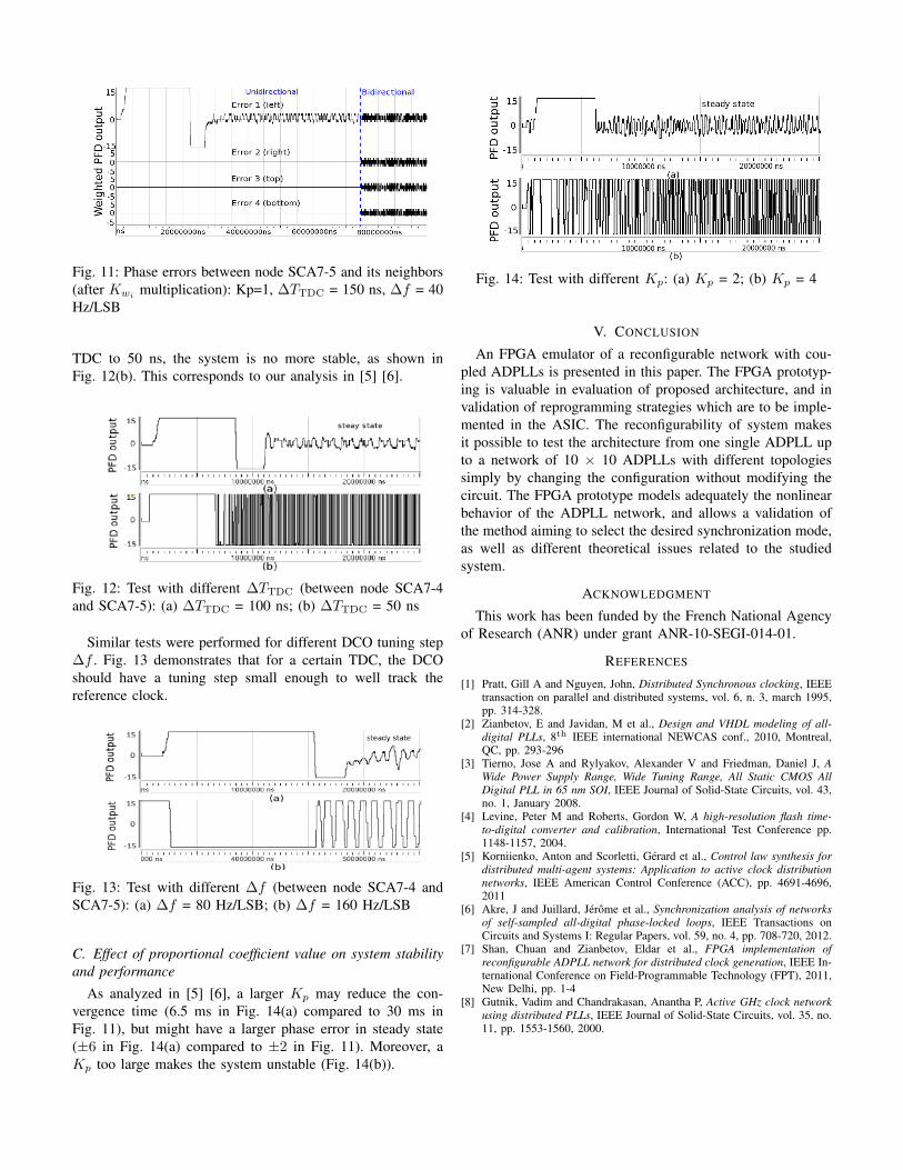
Fig. 11: Phase errors between node SCA7-5 and its neighbors
(after Kwimultiplication): Kp=1, ∆TTDC = 150 ns, ∆f = 40
Hz/LSB
TDC to 50 ns, the system is no more stable, as shown in
Fig. 12(b). This corresponds to our analysis in [5] [6].
Fig. 12: Test with different ∆TTDC (between node SCA7-4
and SCA7-5): (a) ∆TTDC = 100 ns; (b) ∆TTDC = 50 ns
Similar tests were performed for different DCO tuning step
∆f . Fig. 13 demonstrates that for a certain TDC, the DCO
should have a tuning step small enough to well track the
reference clock.
Fig. 13: Test with different ∆f (between node SCA7-4 and
SCA7-5): (a) ∆f = 80 Hz/LSB; (b) ∆f = 160 Hz/LSB
C. Effect of proportional coefficient value on system stability
and performance
As analyzed in [5] [6], a larger Kp may reduce the con-
vergence time (6.5 ms in Fig. 14(a) compared to 30 ms in
Fig. 11), but might have a larger phase error in steady state
(±6 in Fig. 14(a) compared to ±2 in Fig. 11). Moreover, a
Kp too large makes the system unstable (Fig. 14(b)).
Fig. 14: Test with different Kp: (a) Kp = 2; (b) Kp = 4
V. CONCLUSION
An FPGA emulator of a reconfigurable network with cou-
pled ADPLLs is presented in this paper. The FPGA prototyp-
ing is valuable in evaluation of proposed architecture, and in
validation of reprogramming strategies which are to be imple-
mented in the ASIC. The reconfigurability of system makes
it possible to test the architecture from one single ADPLL up
to a network of 10 × 10 ADPLLs with different topologies
simply by changing the configuration without modifying the
circuit. The FPGA prototype models adequately the nonlinear
behavior of the ADPLL network, and allows a validation of
the method aiming to select the desired synchronization mode,
as well as different theoretical issues related to the studied
system.
ACKNOWLEDGMENT
This work has been funded by the French National Agency
of Research (ANR) under grant ANR-10-SEGI-014-01.
REFERENCES
[1] Pratt, Gill A and Nguyen, John, Distributed Synchronous clocking, IEEEtransaction on parallel and distributed systems, vol. 6, n. 3, march 1995,pp. 314-328.
[2] Zianbetov, E and Javidan, M et al., Design and VHDL modeling of all-
digital PLLs, 8th IEEE international NEWCAS conf., 2010, Montreal,QC, pp. 293-296
[3] Tierno, Jose A and Rylyakov, Alexander V and Friedman, Daniel J, A
Wide Power Supply Range, Wide Tuning Range, All Static CMOS All
Digital PLL in 65 nm SOI, IEEE Journal of Solid-State Circuits, vol. 43,no. 1, January 2008.
[4] Levine, Peter M and Roberts, Gordon W, A high-resolution flash time-
to-digital converter and calibration, International Test Conference pp.1148-1157, 2004.
[5] Korniienko, Anton and Scorletti, Gerard et al., Control law synthesis for
distributed multi-agent systems: Application to active clock distribution
networks, IEEE American Control Conference (ACC), pp. 4691-4696,2011
[6] Akre, J and Juillard, Jerome et al., Synchronization analysis of networks
of self-sampled all-digital phase-locked loops, IEEE Transactions onCircuits and Systems I: Regular Papers, vol. 59, no. 4, pp. 708-720, 2012.
[7] Shan, Chuan and Zianbetov, Eldar et al., FPGA implementation of
reconfigurable ADPLL network for distributed clock generation, IEEE In-ternational Conference on Field-Programmable Technology (FPT), 2011,New Delhi, pp. 1-4
[8] Gutnik, Vadim and Chandrakasan, Anantha P, Active GHz clock network
using distributed PLLs, IEEE Journal of Solid-State Circuits, vol. 35, no.11, pp. 1553-1560, 2000.