Embed Size (px)
Citation preview
1
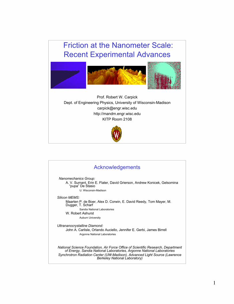
Friction at the Nanometer Scale:Recent Experimental Advances
Prof. Robert W. CarpickDept. of Engineering Physics, University of Wisconsin-Madison
[email protected]://mandm.engr.wisc.edu
KITP Room 2108
Acknowledgements
Nanomechanics Group:A. V. Sumant, Erin E. Flater, David Grierson, Andrew Konicek, Gelsomina
“pupa” De StasioU. Wisconsin-Madison
Silicon MEMS:Maarten P. de Boer, Alex D. Corwin, E. David Reedy, Tom Mayer, M. Dugger, T. Scharf
Sandia National LaboratoriesW. Robert Ashurst
Auburn University
Ultrananocrystalline Diamond:John A. Carlisle, Orlando Auciello, Jennifer E. Gerbi, James Birrell
Argonne National Laboratories
National Science Foundation, Air Force Office of Scientific Research, Departmentof Energy, Sandia National Laboratories, Argonne National Laboratories
Synchrotron Radiation Center (UW-Madison), Advanced Light Source (LawrenceBerkeley National Laboratory)
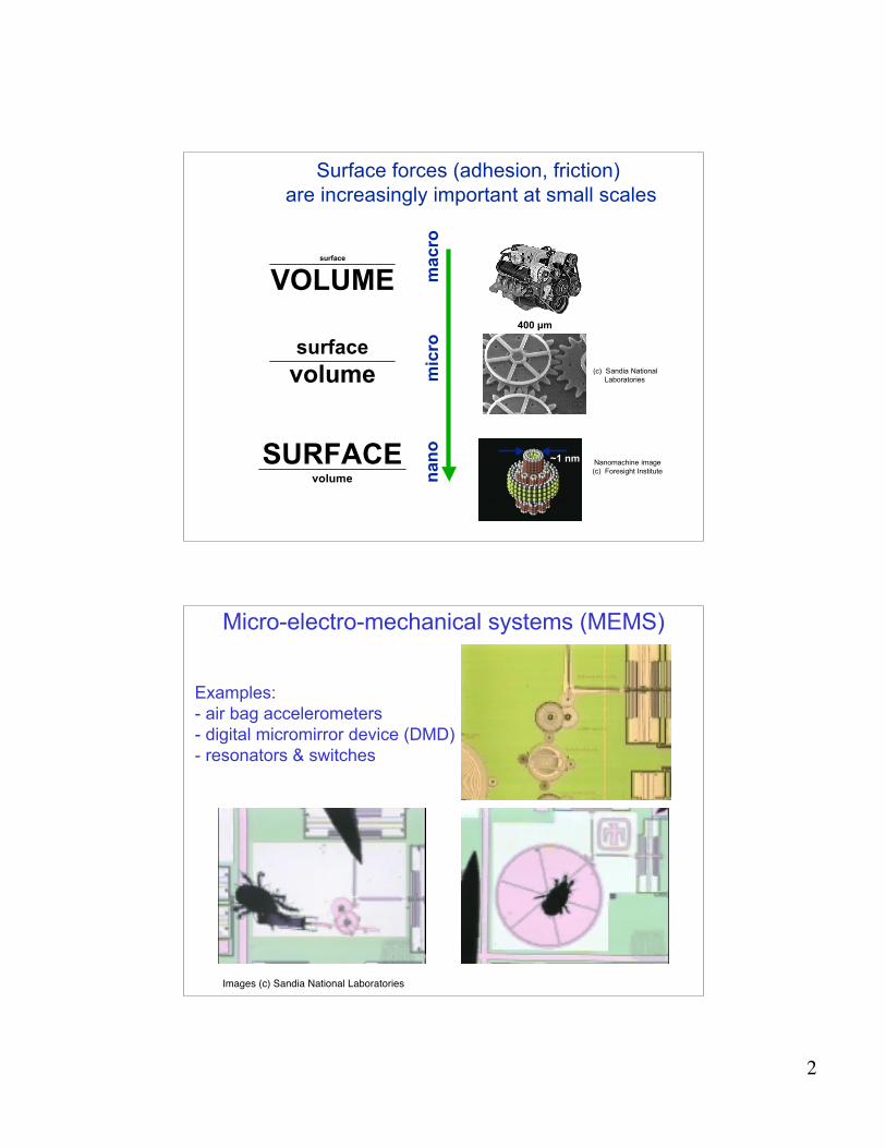
2
surface
VOLUME mac
ro
surfacevolume
Micromachine image(c) Sandia National
Laboratoriesmic
ro
400 µm
SURFACEvolume na
no ~1 nm Nanomachine image(c) Foresight Institute
Surface forces (adhesion, friction) are increasingly important at small scales
Images (c) Sandia National Laboratories
Micro-electro-mechanical systems (MEMS)
Examples:- air bag accelerometers- digital micromirror device (DMD)- resonators & switches
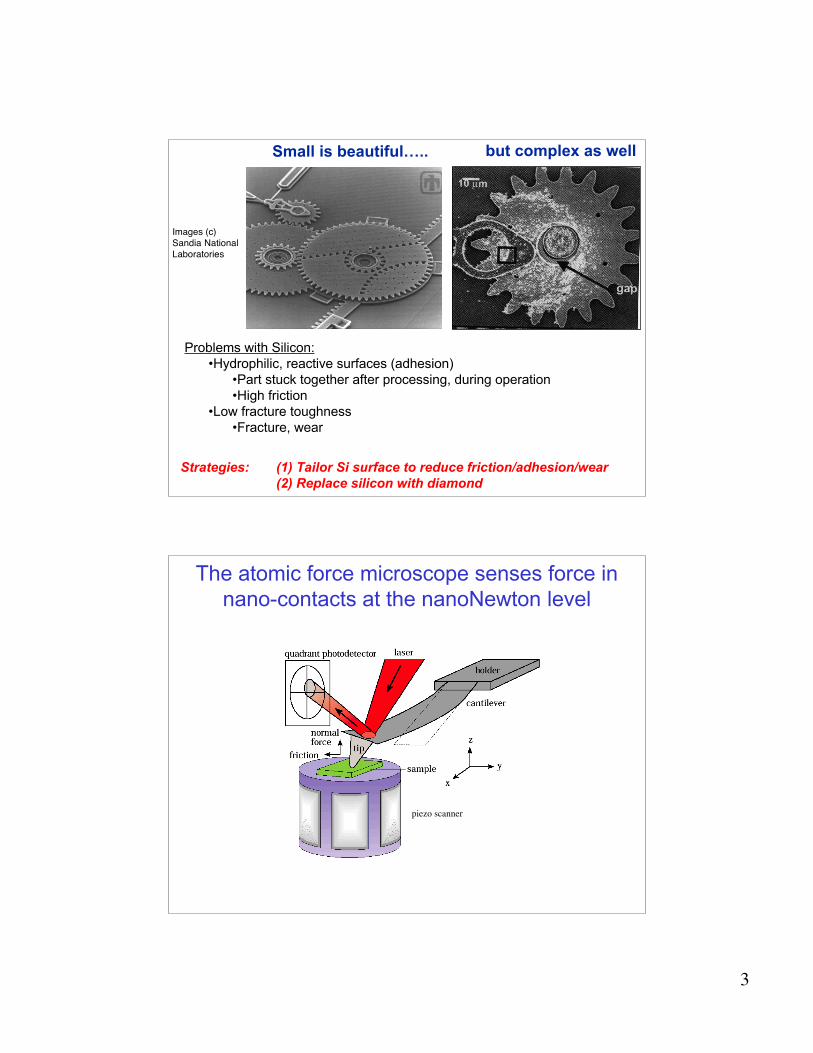
3
Images (c)Sandia NationalLaboratories
Small is beautiful…..
Problems with Silicon:•Hydrophilic, reactive surfaces (adhesion)
•Part stuck together after processing, during operation•High friction
•Low fracture toughness•Fracture, wear
but complex as well
Strategies: (1) Tailor Si surface to reduce friction/adhesion/wear(2) Replace silicon with diamond
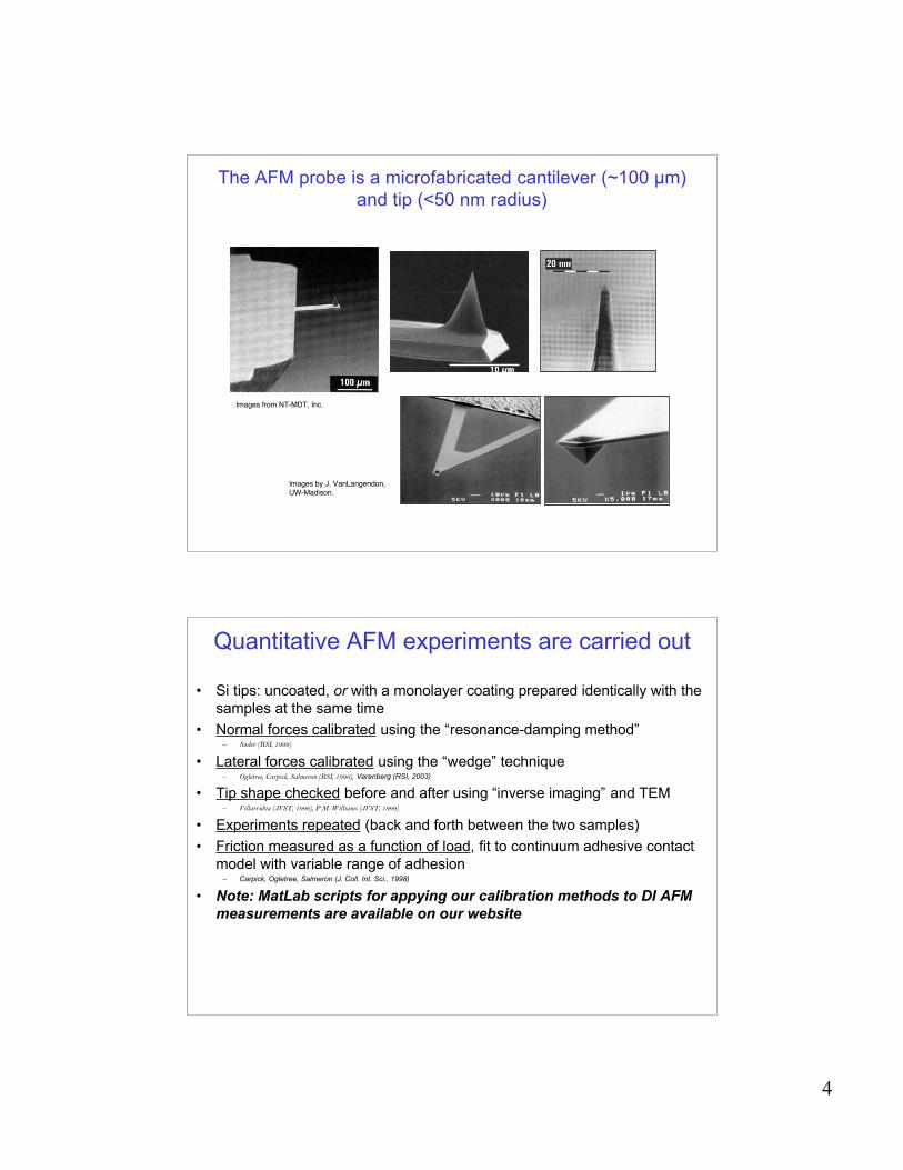
The atomic force microscope senses force innano-contacts at the nanoNewton level
piezo scanner
4
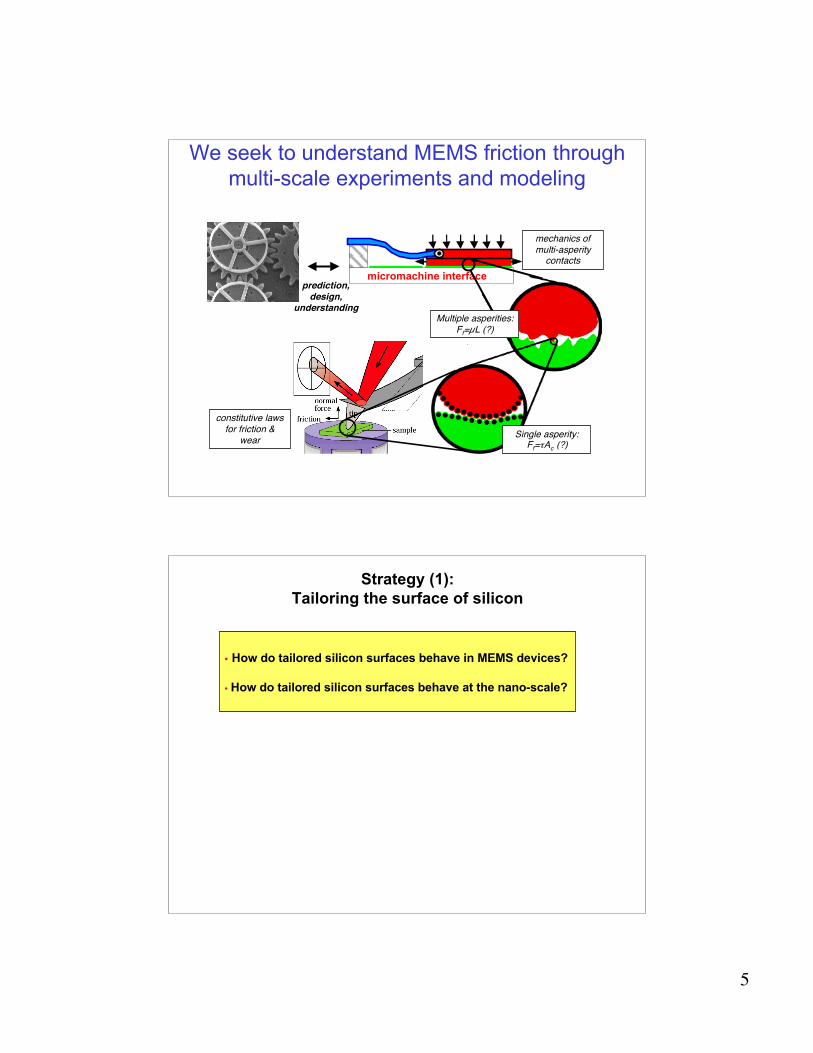
The AFM probe is a microfabricated cantilever (~100 µm)and tip (<50 nm radius)
Images from NT-MDT, Inc.
Images by J. VanLangendon,UW-Madison.
Quantitative AFM experiments are carried out
• Si tips: uncoated, or with a monolayer coating prepared identically with thesamples at the same time
• Normal forces calibrated using the “resonance-damping method”– Sader (RSI, 1999)
• Lateral forces calibrated using the “wedge” technique– Ogletree, Carpick, Salmeron (RSI, 1996), Varenberg (RSI, 2003)
• Tip shape checked before and after using “inverse imaging” and TEM– Villarrubia (JVST, 1996), P.M. Williams (JVST, 1999)
• Experiments repeated (back and forth between the two samples)• Friction measured as a function of load, fit to continuum adhesive contact
model with variable range of adhesion– Carpick, Ogletree, Salmeron (J. Coll. Int. Sci., 1998)
• Note: MatLab scripts for appying our calibration methods to DI AFMmeasurements are available on our website
5
We seek to understand MEMS friction throughmulti-scale experiments and modeling
micromachine interfaceprediction,design,
understanding
constitutive lawsfor friction &
wear
mechanics ofmulti-asperity
contacts
Single asperity:Ff=τAc (?)
Multiple asperities:Ff=µL (?)
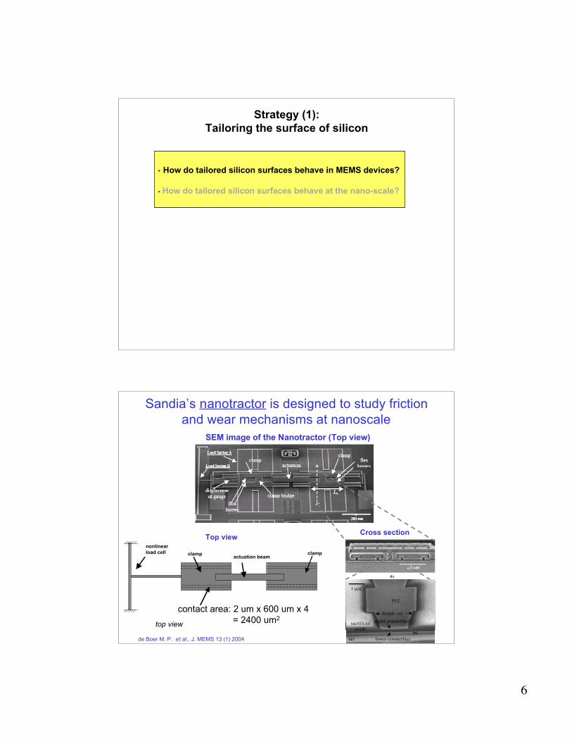
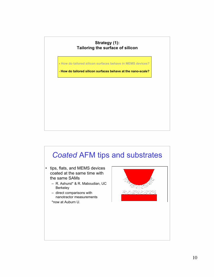
• How do tailored silicon surfaces behave in MEMS devices? • How do tailored silicon surfaces behave at the nano-scale?
Strategy (1):Tailoring the surface of silicon
6
• How do tailored silicon surfaces behave in MEMS devices? • How do tailored silicon surfaces behave at the nano-scale?
Strategy (1):Tailoring the surface of silicon
Sandia’s nanotractor is designed to study frictionand wear mechanisms at nanoscale
actuation beamclamp clamp
nonlinear
load cell
contact area: 2 um x 600 um x 4
= 2400 um2
top view
Cross section
Sliding Counterface
Si surface coated with SAM
SEM image of the Nanotractor (Top view)
Top view
de Boer M. P. et al., J. MEMS 13 (1) 2004
1 µm
(c)
P0
dimple cut
upper counterface
P12
sacrificial
oxide
lower counterface
7
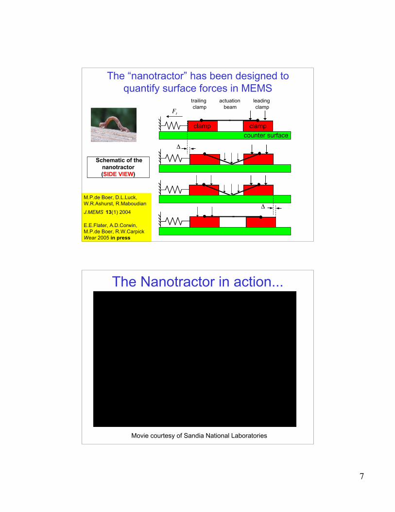
The “nanotractor” has been designed toquantify surface forces in MEMS
Schematic of thenanotractor(SIDE VIEW)
trailing actuation leading clamp beam clamp
clamp clamp
Ft
counter surface
Δ
Δ
M.P.de Boer, D.L.Luck,W.R.Ashurst, R.Maboudian
J.MEMS 13(1) 2004
E.E.Flater, A.D.Corwin,M.P.de Boer, R.W.CarpickWear 2005 in press
The Nanotractor in action...
Movie courtesy of Sandia National Laboratories
8
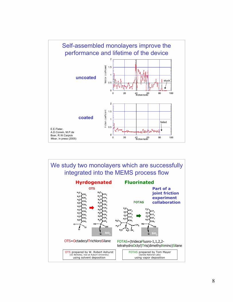
Self-assembled monolayers improve theperformance and lifetime of the device
uncoated
coated
E.E.Flater,A.D.Corwin, M.P.deBoer, R.W.CarpickWear, in press (2005)
stuck
failed
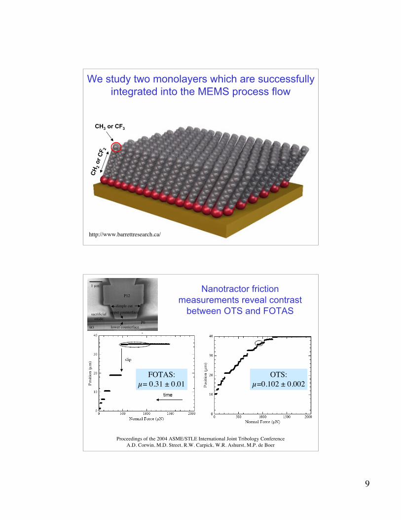
We study two monolayers which are successfullyintegrated into the MEMS process flow
OTS prepared by W. Robert Ashurst(UC Berkeley, now at Auburn University)
using solvent deposition
FOTAS prepared by Tom Mayer(Sandia National Labs)
using vapor deposition
OTS=OctadecylTrichloroSilane FOTAS=(tridecaFluoro-1,1,2,2-tetrahydroOctyl)Tris(dimethylAmino)Silane
Hyrdogenated FluorinatedPart of ajoint frictionexperimentcollaboration
9
http://www.barrettresearch.ca/
We study two monolayers which are successfullyintegrated into the MEMS process flow
CH2 o
r CF 2
CH3 or CF3
Nanotractor frictionmeasurements reveal contrast
between OTS and FOTAS
Proceedings of the 2004 ASME/STLE International Joint Tribology ConferenceA.D. Corwin, M.D. Street, R.W. Carpick, W.R. Ashurst, M.P. de Boer
1 µm
(c)P0
dimple cutupper counterface
P12
sacrificialoxide
lower counterface
FOTAS:µ= 0.31 ± 0.01
OTS:µ=0.102 ± 0.002
10
• How do tailored silicon surfaces behave in MEMS devices? • How do tailored silicon surfaces behave at the nano-scale?
Strategy (1):Tailoring the surface of silicon
Coated AFM tips and substrates• tips, flats, and MEMS devices
coated at the same time withthe same SAMs– R. Ashurst* & R. Maboudian, UC
Berkeley– direct comparisons with
nanotractor measurements*now at Auburn U.
11
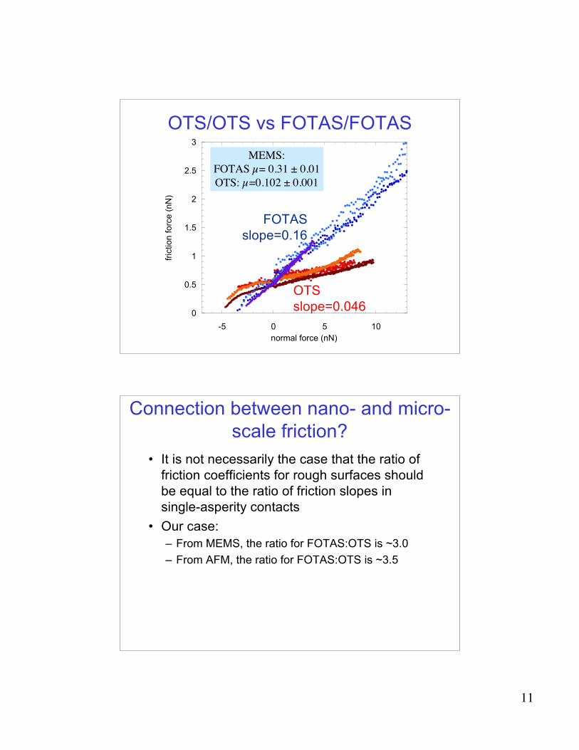
OTS/OTS vs FOTAS/FOTAS
0
0.5
1
1.5
2
2.5
3
-5 0 5 10
fric
tio
n f
orc
e (
nN
)
normal force (nN)
OTSslope=0.046
FOTASslope=0.16
MEMS:FOTAS µ= 0.31 ± 0.01OTS: µ=0.102 ± 0.001
Connection between nano- and micro-scale friction?
• It is not necessarily the case that the ratio offriction coefficients for rough surfaces shouldbe equal to the ratio of friction slopes insingle-asperity contacts
• Our case:– From MEMS, the ratio for FOTAS:OTS is ~3.0– From AFM, the ratio for FOTAS:OTS is ~3.5
12
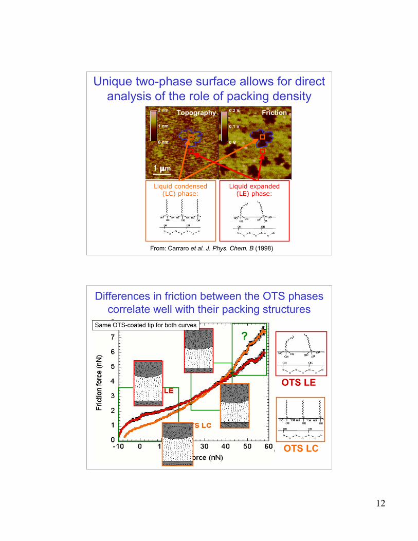
Unique two-phase surface allows for directanalysis of the role of packing density
1 µm
Topography Friction0.2 V
0.1 V
0 V
2 nm
1 nm
0 nm
From: Carraro et al. J. Phys. Chem. B (1998)
Liquid condensed(LC) phase:
Liquid expanded(LE) phase:
OTS LE
OTS LC
Differences in friction between the OTS phasescorrelate well with their packing structures
?Same OTS-coated tip for both curves
13
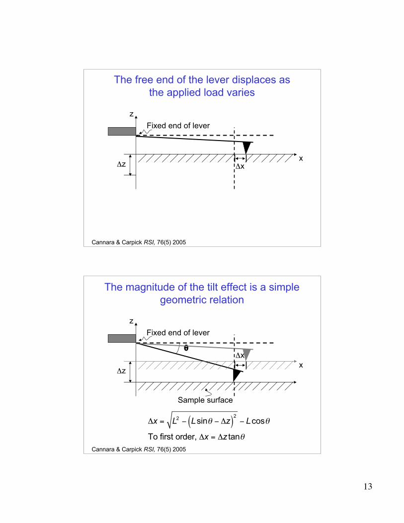
The free end of the lever displaces asthe applied load varies
zFixed end of lever
xSample surface
θ
Δz Δxx
Cannara & Carpick RSI, 76(5) 2005
The magnitude of the tilt effect is a simplegeometric relation
Sample surface
θ
zFixed end of lever
Δzx
Δx
Cannara & Carpick RSI, 76(5) 2005
!x = L2" Lsin# " !z( )
2
" Lcos#
To first order, !x = !z tan#

14
Tilt-compensation allows one to staywithin the intended region of analysis
z
xSample surface
θ
Δzx
Δx
Cannara & Carpick RSI, 76(5) 2005
Friction measurements depend onlocation on sample
1 µm
0.1 V
0.05 V
0 V
500 nmFriction
15
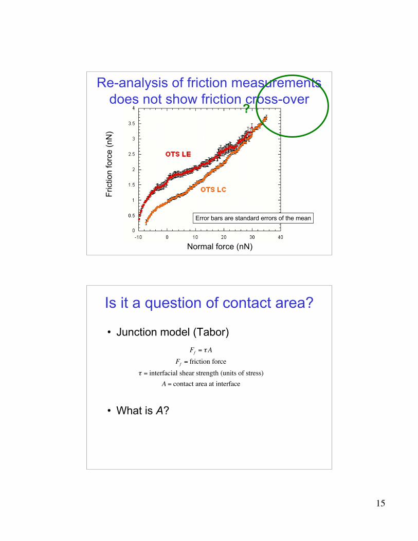
Re-analysis of friction measurementsdoes not show friction cross-over
Normal force (nN)
Fric
tion
forc
e (n
N)
Error bars are standard errors of the mean
?
Is it a question of contact area?
• Junction model (Tabor)
• What is A?
Ff = !A
Ff = friction force
! = interfacial shear strength (units of stress)
A = contact area at interface
16
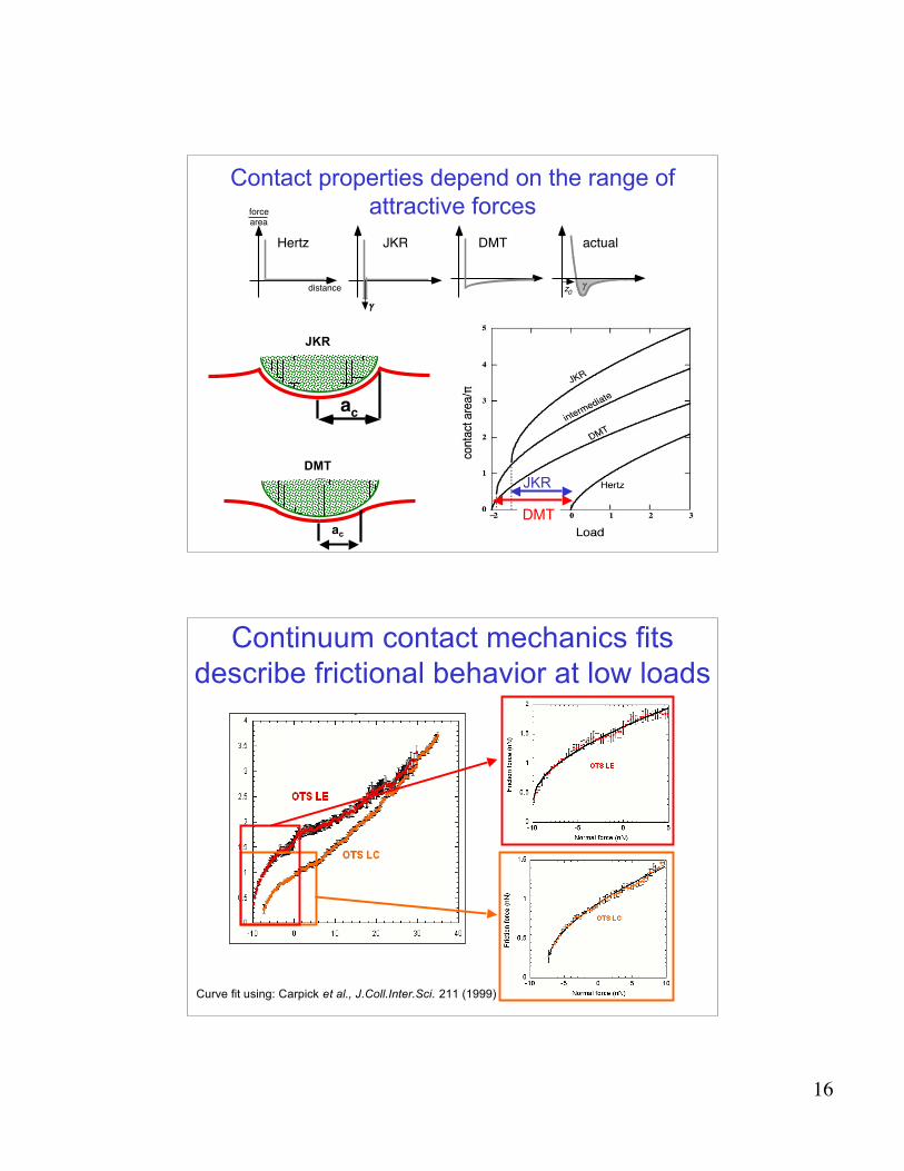
Contact properties depend on the range ofattractive forces
actual
z0
!
force
area
distance
Hertz
!
JKR DMT
figure 1
ac
JKR
DMT
ac
JKR
DMT
Continuum contact mechanics fitsdescribe frictional behavior at low loads
Curve fit using: Carpick et al., J.Coll.Inter.Sci. 211 (1999)
17
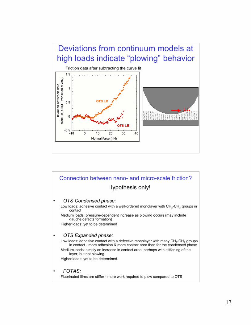
Deviations from continuum models athigh loads indicate “plowing” behavior
Friction data after subtracting the curve fit
Connection between nano- and micro-scale friction?Hypothesis only!
• OTS Condensed phase:Low loads: adhesive contact with a well-ordered monolayer with CH3-CH3 groups in
contactMedium loads: pressure-dependent increase as plowing occurs (may include
gauche defects formation)Higher loads: yet to be determined
• OTS Expanded phase:Low loads: adhesive contact with a defective monolayer with many CH2-CH2 groups
in contact - more adhesion & more contact area than for the condensed phaseMedium loads: simply an increase in contact area, perhaps with stiffening of the
layer, but not plowingHigher loads: yet to be determined.
• FOTAS:Fluorinated films are stiffer - more work required to plow compared to OTS
18
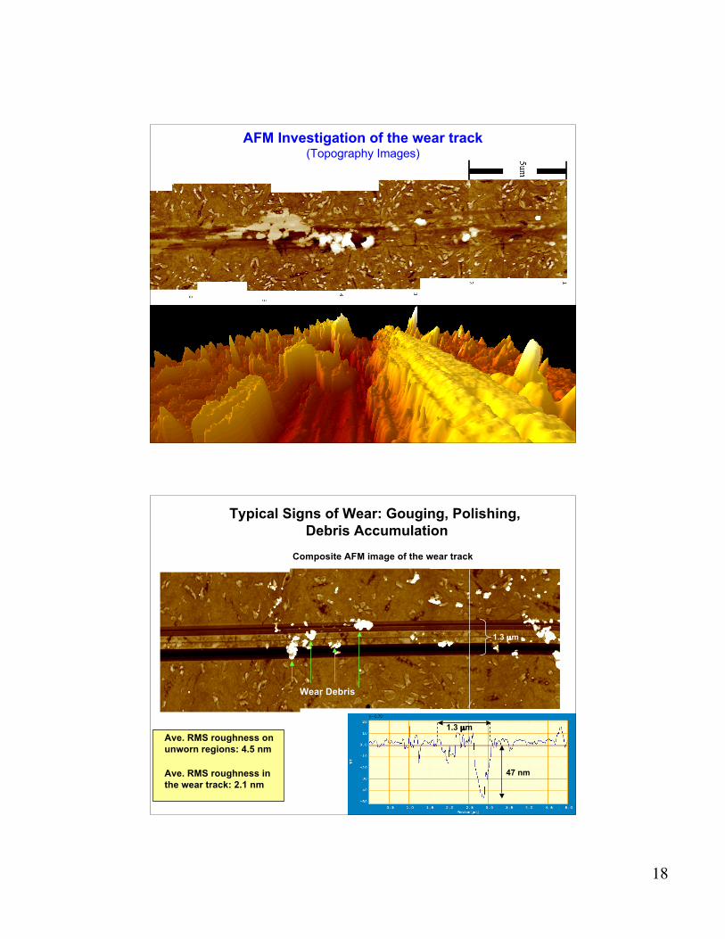
AFM Investigation of the wear track(Topography Images)
Chip 2 – Device 2 – AOI 6
West Side of NE TrackComposite AFM image of the wear track
Typical Signs of Wear: Gouging, Polishing, Debris Accumulation
Ave. RMS roughness on unworn regions: 4.5 nm
Ave. RMS roughness in the wear track: 2.1 nm
1.3 µm
47 nm
1.3 µm
Wear Debris
19
Conclusions• SAM coatings substantially modify friction in MEMS, as determinedby their molecular architecture
• AFM single asperity measurements can be used to understandlarger-scale friction behavior in MEMS• Tribochemical changes occur during wear processes in MEMS,and we need to study these further
•UNCD is a promising structural material for MEMS• Lower friction and adhesion than silicon at the nano-scale• Post growth H-plasma improves the surface chemistry andnanotribology of the bottom side. Adhesion approaches the vander waals limit; friction is correspondingly low.
⇒ Is this the ideal tribological surface?
•Tribology + imaging + spectroscopy = understanding friction?
Thank you

![Untersuchungen zur Haftkraft - berechnung bei der ... · Das Modell nach Johnson, Kendall und Roberts (JKR) [16] basiert wie das DMT-Modell auf der Hertz-Theorie und geht von einer](https://img.pdfslide.net/doc/110x75/5d4f17d388c993720d8b95cf/untersuchungen-zur-haftkraft-berechnung-bei-der-das-modell-nach-johnson.jpg)


![BORANG BERKAITANepsmg.jkr.gov.my/images/archive/1/15/20160202011736...*Pohon rujuk Manual pH JKR untuk keterangan terperinci bagi setiap pengemukaan [JKR/pH JKR/BRG02-KB1.1] pH JKR(JKR20801-0014-15)](https://img.pdfslide.net/doc/110x75/5e5a0ea9a5d37b193b1f29d9/borang-pohon-rujuk-manual-ph-jkr-untuk-keterangan-terperinci-bagi-setiap-pengemukaan.jpg)
![Numerical investigation of indentation tests on a ...bingweb.binghamton.edu/~cjin/publications/adh.pdf · (JKR) model,[] the Derjaguin–Muller–Toporov (DMT) model,[5 ] and the](https://img.pdfslide.net/doc/110x75/5e6c36f2785f3e2d4323bf4e/numerical-investigation-of-indentation-tests-on-a-cjinpublicationsadhpdf.jpg)