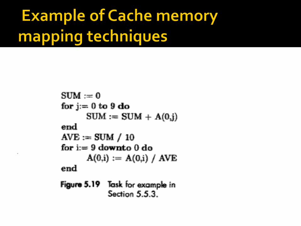
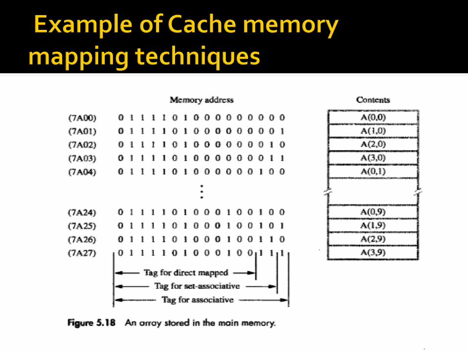
Embed Size (px)
Citation preview

Fundamental Concepts

Maximum size of the Main Memorybyte-addressableCPU-Main Memory Connection
Up to 2 k addressableMDR
MAR
k-bitaddress bus
n-bitdata bus
Control lines( , MFC, etc.)
Processor Memory
locations
Word length = n bits
WR /
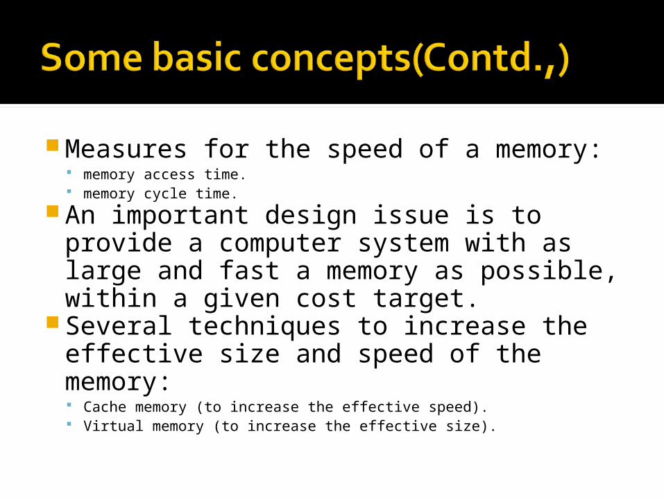
Measures for the speed of a memory: memory access time. memory cycle time.
An important design issue is to provide a computer system with as large and fast a memory as possible, within a given cost target.
Several techniques to increase the effective size and speed of the memory: Cache memory (to increase the effective speed). Virtual memory (to increase the effective size).
Semiconductor RAM memories
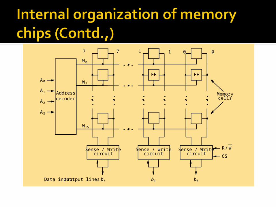
Each memory cell can hold one bit of information. Memory cells are organized in the form of an array. One row is one memory word. All cells of a row are connected to a common line,
known as the “word line”. Word line is connected to the address decoder. Sense/write circuits are connected to the data
input/output lines of the memory chip.
FF
circuitSense / Write
Addressdecoder
FF
CS
cellsMemory
circuitSense / Write Sense / Write
circuit
Data input /output lines:
A0
A1
A2
A3
W0
W1
W15
7 1 0
WR /
7 1 0
b7 b1 b0
•••
•••
•••
•••
•••
•••
•••
•••
•••
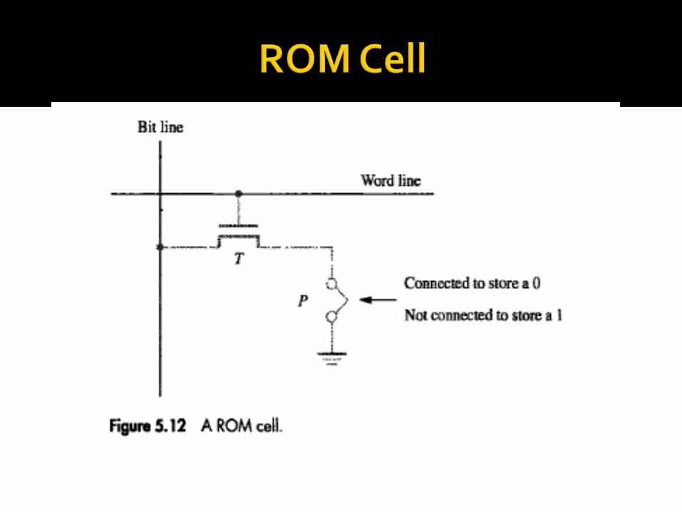
Read-Only Memories (ROMs)
SRAM and SDRAM chips are volatile: Lose the contents when the power is turned off.
Many applications need memory devices to retain contents after the power is turned off. For example, computer is turned on, the operating
system must be loaded from the disk into the memory. Store instructions which would load the OS from the disk. Need to store these instructions so that they will not be
lost after the power is turned off. We need to store the instructions into a non-volatile
memory. Non-volatile memory is read in the same manner as
volatile memory. Separate writing process is needed to place information
in this memory. Normal operation involves only reading of data, this type
of memory is called Read-Only memory (ROM).
Read-Only Memory: Data are written into a ROM when it is manufactured.
Programmable Read-Only Memory (PROM): Allow the data to be loaded by a user. Process of inserting the data is irreversible. Storing information specific to a user in a ROM is expensive.
Providing programming capability to a user may be better. Erasable Programmable Read-Only
Memory (EPROM): Stored data to be erased and new data to be loaded. Flexibility, useful during the development phase of digital systems. Erasable, reprogrammable ROM. Erasure requires exposing the ROM to UV light.
Electrically Erasable Programmable Read-Only Memory (EEPROM): To erase the contents of EPROMs, they have to be exposed to ultraviolet light. Physically removed from the circuit. EEPROMs the contents can be stored and erased electrically.
Flash memory: Has similar approach to EEPROM. Read the contents of a single cell, but write the
contents of an entire block of cells. Flash devices have greater density.
▪ Higher capacity and low storage cost per bit.
Power consumption of flash memory is very low, making it attractive for use in equipment that is battery-driven.
Single flash chips are not sufficiently large, so larger memory modules are implemented using flash cards and flash drives.

A big challenge in the design of a computer system is to provide a sufficiently large memory, with a reasonable speed at an affordable cost.
Static RAM: Very fast, but expensive, because a basic SRAM cell has a complex
circuit making it impossible to pack a large number of cells onto a single chip.
Dynamic RAM: Simpler basic cell circuit, hence are much less expensive, but
significantly slower than SRAMs. Magnetic disks:
Storage provided by DRAMs is higher than SRAMs, but is still less than what is necessary.
Secondary storage such as magnetic disks provide a large amount of storage, but is much slower than DRAMs.

Processor
Primarycache
Mainmemory
Increasingsize
Increasingspeed
Magnetic disksecondarymemory
Increasingcost per bit
Registers
L1
Secondarycache
L2
•Fastest access is to the data held in processor registers. Registers are atthe top of the memory hierarchy.•Relatively small amount of memory thatcan be implemented on the processor chip. This is processor cache. •Two levels of cache. Level 1 (L1) cache is on the processor chip. Level 2 (L2) cache is in between main memory and processor. •Next level is main memory, implementedas SIMMs. Much larger, but much slowerthan cache memory.•Next level is magnetic disks. Huge amountof inexepensive storage. •Speed of memory access is critical, the idea is to bring instructions and data that will be used in the near future as close to the processor as possible.

Cache Memories
Processor is much faster than the main memory. As a result, the processor has to spend much of its time waiting while
instructions and data are being fetched from the main memory. Major obstacle towards achieving good performance.
Speed of the main memory cannot be increased beyond a certain point.
Cache memory is an architectural arrangement which makes the main memory appear faster to the processor than it really is.
Cache memory is based on the property of computer programs known as “locality of reference”.
Analysis of programs indicates that many instructions in localized areas of a program are executed repeatedly during some period of time, while the others are accessed relatively less frequently. These instructions may be the ones in a loop, nested loop or few
procedures calling each other repeatedly. This is called “locality of reference”.
Temporal locality of reference: Recently executed instruction is likely to be executed again very
soon. Spatial locality of reference:
Instructions with addresses close to a recently instruction are likely to be executed soon.
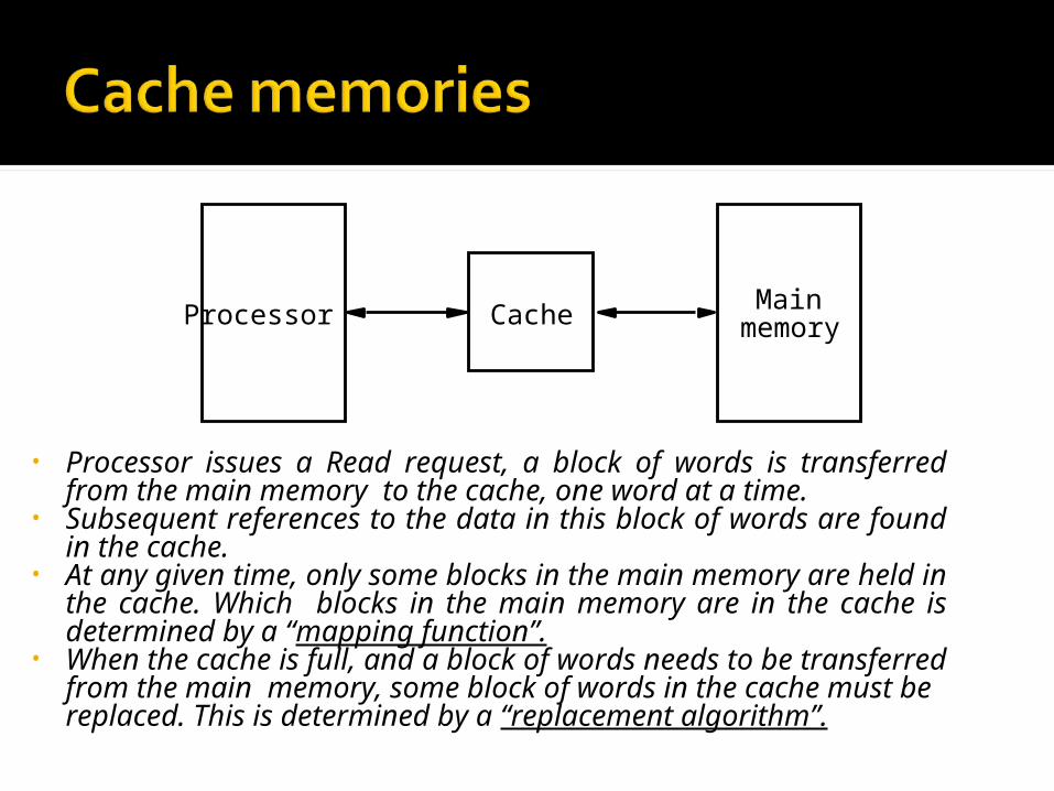
• Processor issues a Read request, a block of words is transferred from the main memory to the cache, one word at a time.
• Subsequent references to the data in this block of words are found in the cache.
• At any given time, only some blocks in the main memory are held in the cache. Which blocks in the main memory are in the cache is determined by a “mapping function”.
• When the cache is full, and a block of words needs to be transferred from the main memory, some block of words in the cache must be replaced. This is determined by a “replacement algorithm”.
Cache MainmemoryProcessor

• Existence of a cache is transparent to the processor. The processor issues Read and Write requests in the same manner.
• If the data is in the cache it is called a Read or Write hit.
• Read hit: The data is obtained from the cache.
• Write hit: Cache has a replica of the contents of the main memory. Contents of the cache and the main memory may be
updated simultaneously. This is the write-through protocol.
Update the contents of the cache, and mark it as updated by setting a bit known as the dirty bit or modified bit. The contents of the main memory are updated when this block is replaced. This is write-back or copy-back protocol.
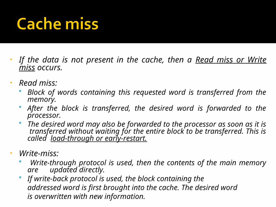
• If the data is not present in the cache, then a Read miss or Write miss occurs.
• Read miss: Block of words containing this requested word is transferred
from the memory. After the block is transferred, the desired word is forwarded to
the processor. The desired word may also be forwarded to the processor as
soon as it is transferred without waiting for the entire block to be transferred. This is called load-through or early-restart.
• Write-miss: Write-through protocol is used, then the contents of the main
memory are updated directly. If write-back protocol is used, the block containing the
addressed word is first brought into the cache. The desired word is overwritten with new information.
• A bit called as “valid bit” is provided for each block.• If the block contains valid data, then the bit is set to 1, else it is 0. • Valid bits are set to 0, when the power is just turned on.• When a block is loaded into the cache for the first time, the valid
bit is set to 1.
• Data transfers between main memory and disk occur directly bypassing the cache.
• When the data on a disk changes, the main memory block is also updated.
• However, if the data is also resident in the cache, then the valid bit is set to 0.
• What happens if the data in the disk and main memory changes and the write-back protocol is being used?
• In this case, the data in the cache may also have changed and is indicated by the dirty bit.
• The copies of the data in the cache, and the main memory are different. This is called the cache coherence problem.
• One option is to force a write-back before the main memory is updated from the disk.
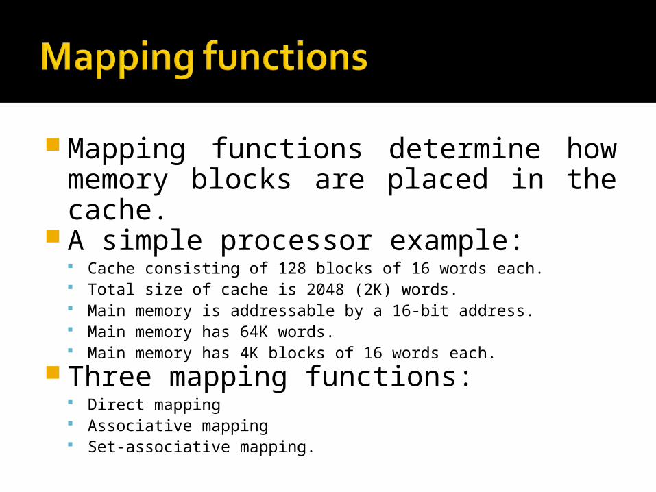
Mapping functions determine how memory blocks are placed in the cache.
A simple processor example: Cache consisting of 128 blocks of 16 words each. Total size of cache is 2048 (2K) words. Main memory is addressable by a 16-bit address. Main memory has 64K words. Main memory has 4K blocks of 16 words each.
Three mapping functions: Direct mapping Associative mapping Set-associative mapping.
Mainmemory Block 0
Block 1
Block 127
Block 128
Block 129
Block 255
Block 256
Block 257
Block 4095
7 4
Main memory address
Tag Block Word
5
tag
tag
tag
Cache
Block 0
Block 1
Block 127
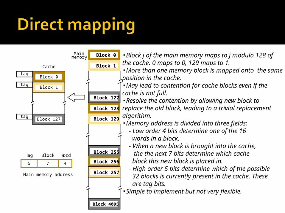
•Block j of the main memory maps to j modulo 128 of the cache. 0 maps to 0, 129 maps to 1.•More than one memory block is mapped onto the same position in the cache.•May lead to contention for cache blocks even if the cache is not full. •Resolve the contention by allowing new block to replace the old block, leading to a trivial replacement algorithm. •Memory address is divided into three fields: - Low order 4 bits determine one of the 16 words in a block. - When a new block is brought into the cache, the the next 7 bits determine which cache block this new block is placed in. - High order 5 bits determine which of the possible 32 blocks is currently present in the cache. These are tag bits.•Simple to implement but not very flexible.
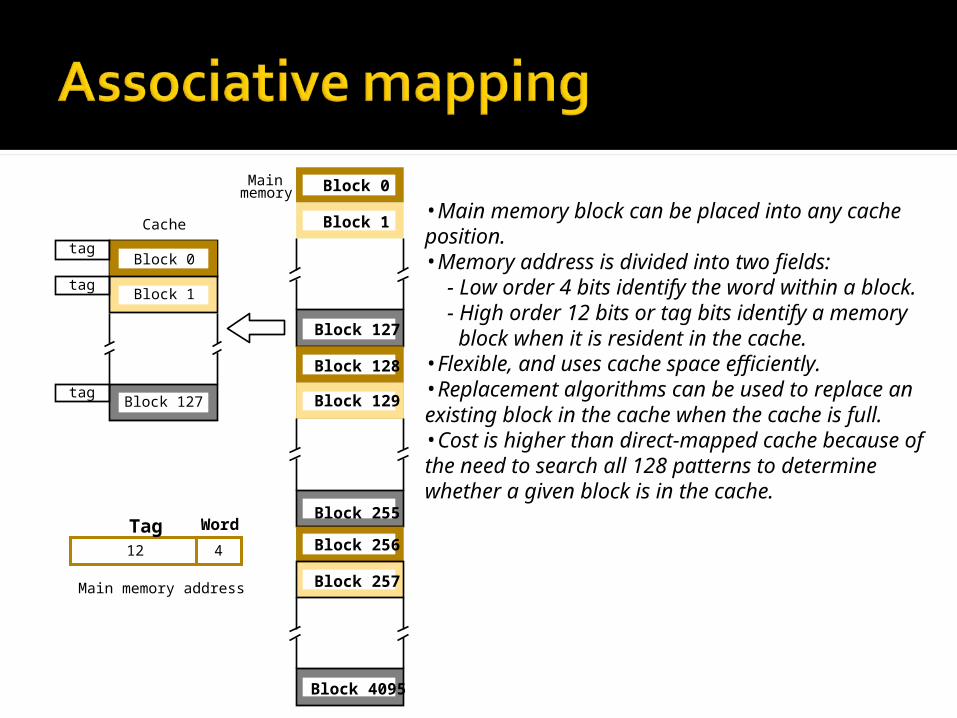
•Main memory block can be placed into any cache position.•Memory address is divided into two fields: - Low order 4 bits identify the word within a block. - High order 12 bits or tag bits identify a memory block when it is resident in the cache. •Flexible, and uses cache space efficiently. •Replacement algorithms can be used to replace anexisting block in the cache when the cache is full. •Cost is higher than direct-mapped cache because of the need to search all 128 patterns to determine whether a given block is in the cache.
Mainmemory Block 0
Block 1
Block 127
Block 128
Block 129
Block 255
Block 256
Block 257
Block 4095
4
Main memory address
Tag Word
12
tag
tag
tag
Cache
Block 0
Block 1
Block 127

Blocks of cache are grouped into sets. Mapping function allows a block of the main memory to reside in any block of a specific set.Divide the cache into 64 sets, with two blocks per set. Memory block 0, 64, 128 etc. map to block 0, and they can occupy either of the two positions.Memory address is divided into three fields: - 6 bit field determines the set number. - High order 6 bit fields are compared to the tag fields of the two blocks in a set.Set-associative mapping combination of direct and associative mapping. Number of blocks per set is a design parameter. - One extreme is to have all the blocks in one set, requiring no set bits (fully associative mapping). - Other extreme is to have one block per set, is the same as direct mapping.
Mainmemory Block 0
Block 1
Block 63
Block 64
Block 65
Block 127
Block 128
Block 129
Block 4095
6 4
Main memory address
Tag Set Word
6
tag
tag
tag
Cache
Block 1
Block 2
Block 126
Block 127
Block 3
Block 0tag
tag
tag
SET 1
SET 2
SET 64
•In direct mapping the position of each block is predetermined, no replacement strategy exists.•But in associative and set associative there is some flexibility. When cache is full cache controller has to decide which page to replace.•Most suitable algorithm is Least Recently used(LRU).


68040 Caches•Motorola 68040 caches has two caches included on the processor chip-one used for instructions and the other for data.•Each cache has 4K bytes.•Uses 4-way set associative organization.•It has 64 sets and each of which can hold 4 blocks.•Each block has 4 long words. Each long word has 4 bytes.•In address- LSB 4 bits specify a byte position within a block.•Next 6 bits identify one of 64 sets. Higher order 22 bits constitute the tag.

68040 Caches•Valid bit is set when the corresponding block is first loaded into cache.•Dirty bit is set when long word data are changed during write operation. It remains set until the block is written back into the memory.ARM710T Cache•Organization is similar to the above cache.•Uses 4-way set associative organization.•It has 64 sets and each of which can hold 4 blocks.•Each block has 16 bytes composed of 4 32-bit words. •It uses Write through protocol and random replacement algorithm.

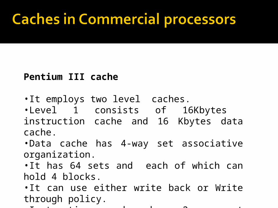
Pentium III cache
•It employs two level caches.•Level 1 consists of 16Kbytes instruction cache and 16 Kbytes data cache.•Data cache has 4-way set associative organization.•It has 64 sets and each of which can hold 4 blocks.•It can use either write back or Write through policy.•Instruction cache has 2-way set associative organization.
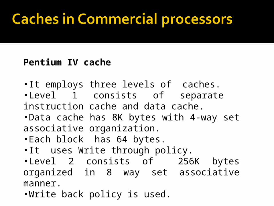
Pentium IV cache
•It employs three levels of caches.•Level 1 consists of separate instruction cache and data cache.•Data cache has 8K bytes with 4-way set associative organization.•Each block has 64 bytes.•It uses Write through policy.•Level 2 consists of 256K bytes organized in 8 way set associative manner.•Write back policy is used.
Performance considerations

A key design objective of a computer system is to achieve the best possible performance at the lowest possible cost. Price/performance ratio is a common measure of
success. Performance of a processor depends on:
How fast machine instructions can be brought into the processor for execution.
How fast the instructions can be executed.
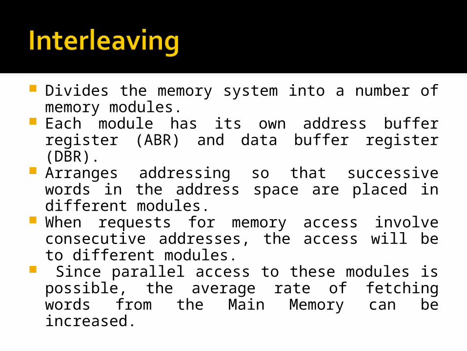
Divides the memory system into a number of memory modules.
Each module has its own address buffer register (ABR) and data buffer register (DBR).
Arranges addressing so that successive words in the address space are placed in different modules.
When requests for memory access involve consecutive addresses, the access will be to different modules.
Since parallel access to these modules is possible, the average rate of fetching words from the Main Memory can be increased.

Consecutive words are placed in a module.
High-order k bits of a memory address determine the module.
Low-order m bits of a memory address determine the word within a module.
When a block of words is transferred from main memory to cache, only one module is busy at a time.
m bits
Address in module MM address
i
k bits
Module Module Module
Module
DBRABR DBRABR ABR DBR
0 n 1- i
k bits
0ModuleModuleModule
Module MM address
DBRABRABR DBRABR DBR
Address in module
2k 1-
m bits
•Consecutive words are located in consecutive modules.•Consecutive addresses can be located in consecutive modules.•While transferring a block of data, several memory modules can be kept busy at the same time.
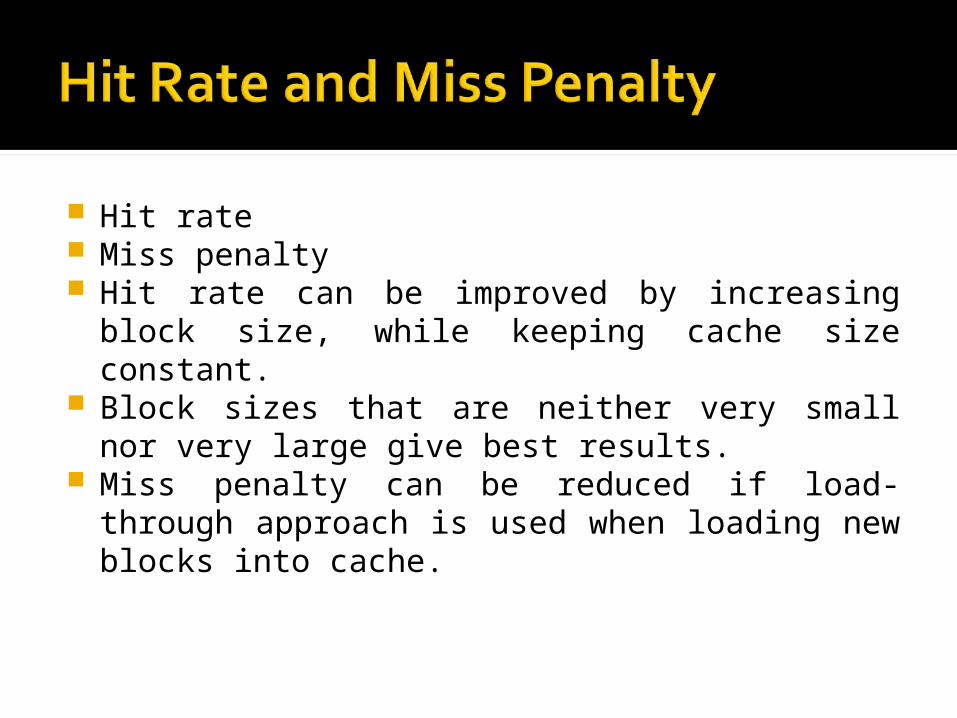
Hit rate Miss penalty Hit rate can be improved by increasing block
size, while keeping cache size constant. Block sizes that are neither very small nor very
large give best results. Miss penalty can be reduced if load-through
approach is used when loading new blocks into cache.
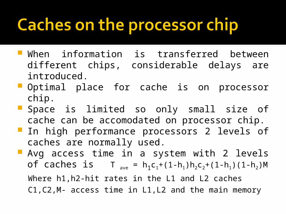
When information is transferred between different chips, considerable delays are introduced.
Optimal place for cache is on processor chip. Space is limited so only small size of cache
can be accomodated on processor chip. In high performance processors 2 levels of
caches are normally used. Avg access time in a system with 2 levels of
caches is T ave = h1c1+(1-h1)h2c2+(1-h1)(1-h2)M
Where h1,h2-hit rates in the L1 and L2 cachesC1,C2,M- access time in L1,L2 and the main memory
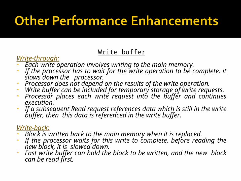
Write bufferWrite-through:• Each write operation involves writing to the main memory.• If the processor has to wait for the write operation to be
complete, it slows down the processor.• Processor does not depend on the results of the write operation.• Write buffer can be included for temporary storage of write
requests.• Processor places each write request into the buffer and
continues execution.• If a subsequent Read request references data which is still in the
write buffer, then this data is referenced in the write buffer.
Write-back:• Block is written back to the main memory when it is replaced. • If the processor waits for this write to complete, before reading
the new block, it is slowed down.• Fast write buffer can hold the block to be written, and the new
block can be read first.

Prefetching• New data are brought into the processor when
they are first needed. • Processor has to wait before the data transfer is
complete. • Prefetch the data into the cache before they are
actually needed, or a before a Read miss occurs. • Prefetching can be accomplished through software
by including a special instruction in the machine language of the processor. Inclusion of prefetch instructions increases the
length of the programs.• Prefetching can also be accomplished using
hardware: Circuitry that attempts to discover patterns in
memory references and then prefetches according to this pattern.

Lockup-Free Cache• Prefetching scheme does not work if it stops
other accesses to the cache until the prefetch is completed.
• A cache of this type is said to be “locked” while it services a miss.
• Cache structure which supports multiple outstanding misses is called a lockup free cache.
• Since only one miss can be serviced at a time, a lockup free cache must include circuits that keep track of all the outstanding misses.
• Special registers may hold the necessary information about these misses.
Virtual Memory

47
Recall that an important challenge in the design of a computer system is to provide a large, fast memory system at an affordable cost.
Architectural solutions to increase the effective speed and size of the memory system.
Cache memories were developed to increase the effective speed of the memory system.
Virtual memory is an architectural solution to increase the effective size of the memory system.
48
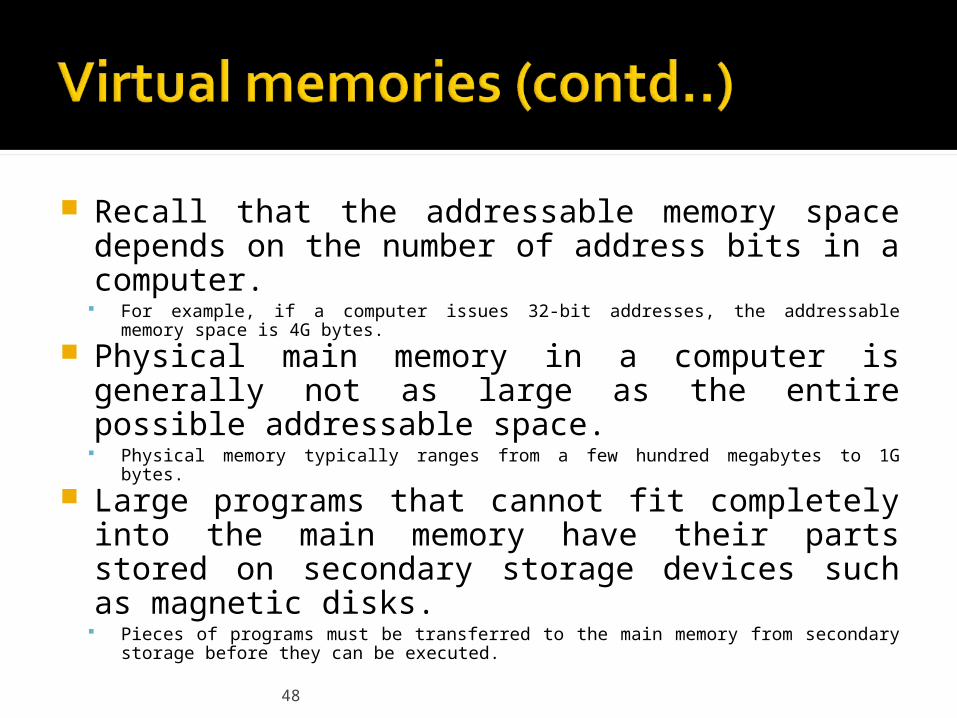
Recall that the addressable memory space depends on the number of address bits in a computer. For example, if a computer issues 32-bit addresses, the addressable memory
space is 4G bytes. Physical main memory in a computer is
generally not as large as the entire possible addressable space. Physical memory typically ranges from a few hundred megabytes to 1G bytes.
Large programs that cannot fit completely into the main memory have their parts stored on secondary storage devices such as magnetic disks. Pieces of programs must be transferred to the main memory from secondary
storage before they can be executed.
49
When a new piece of a program is to be transferred to the main memory, and the main memory is full, then some other piece in the main memory must be replaced. Recall this is very similar to what we studied in case of cache
memories. Operating system automatically
transfers data between the main memory and secondary storage. Application programmer need not be concerned with this transfer. Also, application programmer does not need to be aware of the
limitations imposed by the available physical memory.
50
Techniques that automatically move program and data between main memory and secondary storage when they are required for execution are called virtual-memory techniques.
Programs and processors reference an instruction or data independent of the size of the main memory.
Processor issues binary addresses for instructions and data. These binary addresses are called logical or virtual addresses.
Virtual addresses are translated into physical addresses by a combination of hardware and software subsystems. If virtual address refers to a part of the program that is currently in the main
memory, it is accessed immediately. If the address refers to a part of the program that is not currently in the main
memory, it is first transferred to the main memory before it can be used.
51
Data
Data
DMA transfer
Physical address
Physical address
Virtual address
Disk storage
Main memory
Cache
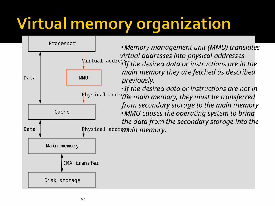
MMU
Processor•Memory management unit (MMU) translatesvirtual addresses into physical addresses. •If the desired data or instructions are in the main memory they are fetched as described previously.•If the desired data or instructions are not in the main memory, they must be transferred from secondary storage to the main memory.•MMU causes the operating system to bring the data from the secondary storage into the main memory.

52
Assume that program and data are composed of fixed-length units called pages.
A page consists of a block of words that occupy contiguous locations in the main memory.
Page is a basic unit of information that is transferred between secondary storage and main memory.
Size of a page commonly ranges from 2K to 16K bytes. Pages should not be too small, because the access time of a secondary
storage device is much larger than the main memory. Pages should not be too large, else a large portion of the page may not
be used, and it will occupy valuable space in the main memory.

53
Concepts of virtual memory are similar to the concepts of cache memory.
Cache memory: Introduced to bridge the speed gap between the processor and
the main memory. Implemented in hardware.
Virtual memory: Introduced to bridge the speed gap between the main memory
and secondary storage. Implemented in part by software.
54
Each virtual or logical address generated by a processor is interpreted as a virtual page number (high-order bits) plus an offset (low-order bits) that specifies the location of a particular byte within that page.
Information about the main memory location of each page is kept in the page table. Main memory address where the page is stored. Current status of the page.
Area of the main memory that can hold a page is called as page frame.
Starting address of the page table is kept in a page table base register.
55
Virtual page number generated by the processor is added to the contents of the page table base register. This provides the address of the corresponding entry in the page
table. The contents of this location in the
page table give the starting address of the page if the page is currently in the main memory.

56
Page frame
Virtual address from processor
in memory
Offset
Offset
Virtual page numberPage table address
Page table base register
Controlbits
Physical address in main memory
PAGE TABLE
Page frame
+
Virtual address isinterpreted as pagenumber and offset.
Page table holds informationabout each page. This includesthe starting address of the page in the main memory.
PTBR holdsthe address of the page table.
PTBR + virtualpage number providethe entry of the page in the page table.
This entry has the starting locationof the page.
57
Page table entry for a page also includes some control bits which describe the status of the page while it is in the main memory.
One bit indicates the validity of the page. Indicates whether the page is actually loaded into the main memory. Allows the operating system to invalidate the page without actually
removing it. One bit indicates whether the page has
been modified during its residency in the main memory. This bit determines whether the page should be written back to the
disk when it is removed from the main memory. Similar to the dirty or modified bit in case of cache memory.
58
Other control bits for various other types of restrictions that may be imposed. For example, a program may only have read permission for a
page, but not write or modify permissions.
59
Where should the page table be located? Recall that the page table is used by the MMU
for every read and write access to the memory. Ideal location for the page table is within the MMU.
Page table is quite large. MMU is implemented as part of the processor
chip. Impossible to include a complete page table on
the chip. Page table is kept in the main memory. A copy of a small portion of the page table can
be accommodated within the MMU. Portion consists of page table entries that correspond to the most recently
accessed pages.
60
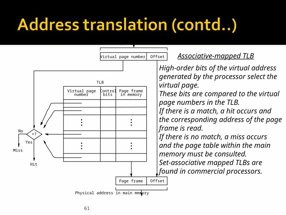
A small cache called as Translation Look aside Buffer (TLB) is included in the MMU. TLB holds page table entries of the most recently accessed pages.
Recall that cache memory holds most recently accessed blocks from the main memory. Operation of the TLB and page table in the main memory is similar to
the operation of the cache and main memory. Page table entry for a page includes:
Address of the page frame where the page resides in the main memory. Some control bits.
In addition to the above for each page, TLB must hold the virtual page number for each page.
61
No
Yes
Hit
Miss
Virtual address from processor
TLB
OffsetVirtual page number
numberVirtual page Page frame
in memoryControl
bits
OffsetPage frame
=?
Physical address in main memory
Associative-mapped TLB
High-order bits of the virtual address generated by the processor select the virtual page.These bits are compared to the virtual page numbers in the TLB.If there is a match, a hit occurs and the corresponding address of the pageframe is read. If there is no match, a miss occurs and the page table within the main memory must be consulted.Set-associative mapped TLBs are found in commercial processors.
62
How to keep the entries of the TLB coherent with the contents of the page table in the main memory?
Operating system may change the contents of the page table in the main memory. Simultaneously it must also invalidate the corresponding entries in the
TLB. A control bit is provided in the TLB to
invalidate an entry. If an entry is invalidated, then the TLB gets
the information for that entry from the page table. Follows the same process that it would follow if the entry is not found in
the TLB or if a “miss” occurs.
63
What happens if a program generates an access to a page that is not in the main memory?
In this case, a page fault is said to occur. Whole page must be brought into the main memory from the disk,
before the execution can proceed. Upon detecting a page fault by the
MMU, following actions occur: MMU asks the operating system to intervene by raising an
exception. Processing of the active task which caused the page fault is
interrupted. Control is transferred to the operating system. Operating system copies the requested page from secondary
storage to the main memory. Once the page is copied, control is returned to the task which was
interrupted.
64
Servicing of a page fault requires transferring the requested page from secondary storage to the main memory.
This transfer may incur a long delay. While the page is being transferred the
operating system may: Suspend the execution of the task that caused the page fault. Begin execution of another task whose pages are in the main
memory.
Enables efficient use of the processor.
65
How to ensure that the interrupted task can continue correctly when it resumes execution?
There are two possibilities: Execution of the interrupted task must continue from the point
where it was interrupted. The instruction must be restarted.
Which specific option is followed depends on the design of the processor.
66
When a new page is to be brought into the main memory from secondary storage, the main memory may be full. Some page from the main memory must be replaced with this new page.
How to choose which page to replace? This is similar to the replacement that occurs when the cache is full. The principle of locality of reference (?) can also be applied here. A replacement strategy similar to LRU can be applied.
Since the size of the main memory is relatively larger compared to cache, a relatively large amount of programs and data can be held in the main memory. Minimizes the frequency of transfers between secondary storage and main
memory.
67
A page may be modified during its residency in the main memory.
When should the page be written back to the secondary storage?
Recall that we encountered a similar problem in the context of cache and main memory: Write-through protocol(?) Write-back protocol(?)
Write-through protocol cannot be used, since it will incur a long delay each time a small amount of data is written to the disk.


!["Content-Addressable Memory (CAM) Circuits and ... · Content-Addressable Memory (CAM) Circuits and Architectures: A T utorial and Surv ey ... [22]. As a rule of thumb, the largest](https://img.pdfslide.net/doc/110x75/5b495e157f8b9a2d2f8b491f/content-addressable-memory-cam-circuits-and-content-addressable-memory.jpg)