Embed Size (px)
Citation preview
Future Challenges for Electronics
Manufacturing Highlights from the iNEMI
Technology Roadmap
Grace O’Malley, iNEMI
Manager of European Operations
Nov 02, 2011

Agenda
iNEMI Roadmap Overview
Highlights from Automotive Product Emulator Group
Packaging & Component Substrates Trends
Environmentally Conscious Electronics Activities
Ongoing research efforts
Summary
Q & A
1
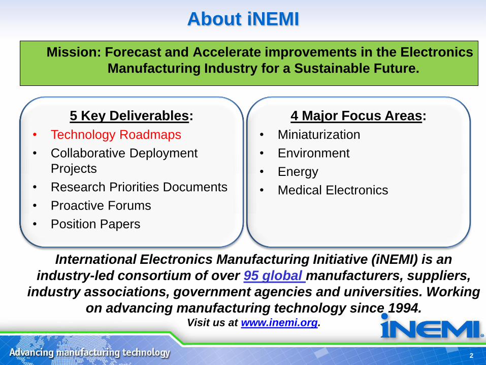
About iNEMI
2
International Electronics Manufacturing Initiative (iNEMI) is an
industry-led consortium of over 95 global manufacturers, suppliers,
industry associations, government agencies and universities. Working
on advancing manufacturing technology since 1994. Visit us at www.inemi.org.
5 Key Deliverables:
• Technology Roadmaps
• Collaborative Deployment
Projects
• Research Priorities Documents
• Proactive Forums
• Position Papers
4 Major Focus Areas:
• Miniaturization
• Environment
• Energy
• Medical Electronics
Mission: Forecast and Accelerate improvements in the Electronics
Manufacturing Industry for a Sustainable Future.

3
Product
Needs
Technology
Evolution
GAP Analysis
Technology Plan
Research
Priorities
Research
Projects
Methodology
Competitive
Solutions
Roadmap
Industry Solution
Needed
Academia
Government
iNEMI
Members
Collaborate
No Work
Required
Available
to Market
Place
Global
Industry
Participation Disruptive
Technology
4 4
iNEMI Roadmap Biannual Process
21 Technology Working Groups (TWGs)
Organic PCB Board
Assembly Customer
RF Components &
Subsystems
Optoelectronics Large Area, Flexible Electronics
Energy Storage &
Conversion Systems
Modeling, Simulation,
and Design
Packaging
&
Component
Substrates
Semiconductor
Technology
Final
Assembly
Mass Storage (Magnetic & Optical)
Passive Components
Information
Management
Systems
Test, Inspection &
Measurement
Environmentally
Conscious
Electronics
Ceramic
Substrates
Thermal
Management
Connectors
MEMS/
Sensors
Red=Business Green=Engineering Purple=Manufacturing Blue=Component & Subsystem
Solid State Illumination
Photovoltaics
5
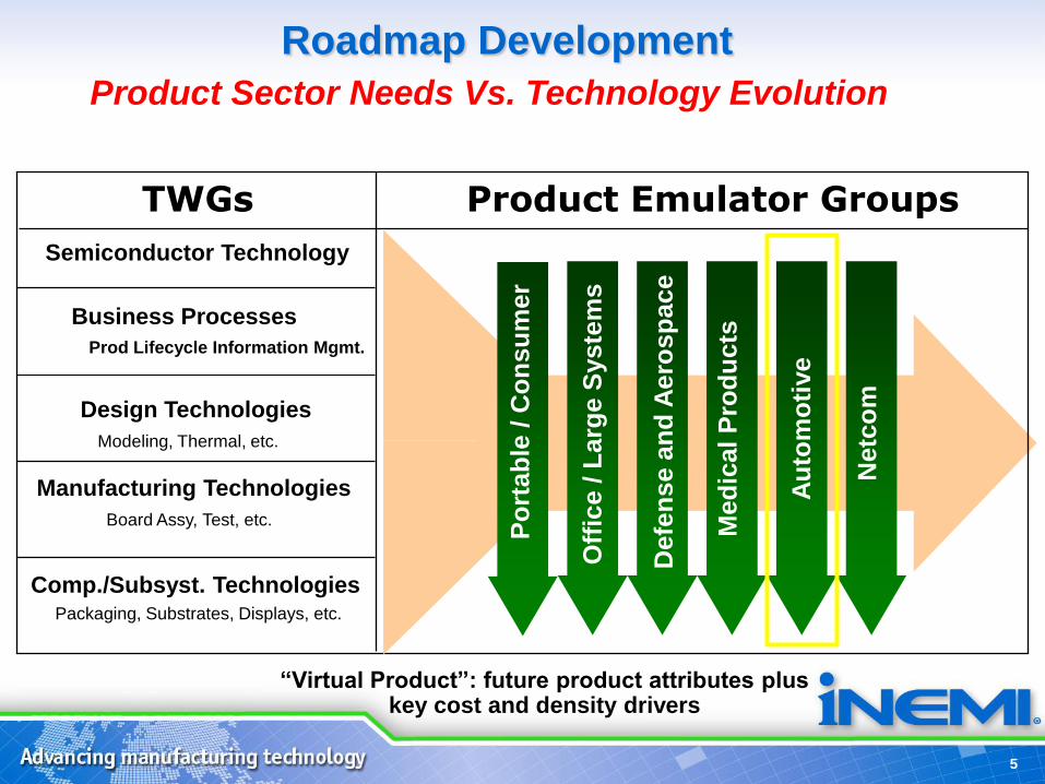
Roadmap Development
Product Emulator Groups TWGs
Med
ical P
rod
ucts
Au
tom
oti
ve
Defe
nse a
nd
Ae
rosp
ace
Semiconductor Technology
Design Technologies
Manufacturing Technologies
Comp./Subsyst. Technologies
Modeling, Thermal, etc.
Board Assy, Test, etc.
Packaging, Substrates, Displays, etc.
Product Sector Needs Vs. Technology Evolution
Business Processes
Prod Lifecycle Information Mgmt.
Po
rtab
le / C
on
su
mer
Off
ice / L
arg
e S
yste
ms
Netc
om
―Virtual Product‖: future product attributes plus key cost and density drivers

6 6
Optoelectronics and
Optical Storage
Organic Printed
Circuit Boards
Magnetic and
Optical Storage
Supply Chain
Management
Semiconductors
iNEMI
Information
Management
TWG
iNEMI
Mass Data
Storage TWG
iNEMI / IPC / EIPC
/ TPCA
Organic PWB
TWG
iNEMI / ITRS /
MIG/PSMA
Packaging
TWG
iNEMI
Board Assembly
TWG
Interconnect
Substrates—Ceramic
iNEMI Roadmap
iNEMI
Optoelectronics
TWG
Thirteen Contributing Industry Organizations
iNEMI / MIG
/ ITRS
MEMS
TWG
iNEMI 2011 RoadMap
Highlights

ELECTRONICS PRODUCTION
2009 - 2021
Note: Total includes product categories not included in iNemi segmentation
$Bn 2009 2011 2013 2015 2021 CAAGR
„09-„15
CAAGR
„15-„21
Computers and Office $396 $433 $474 $500 $617 4.0% 3.6%
Communications Infrastructure Equipment $157 $174 $192 $213 $281 5.2% 4.7%
Consumer and Portable Electronics $298 $319 $341 $400 $479 5.0% 3.1%
Automotive Electronics $105 $129 $158 $161 $237 7.4% 6.6%
Medical Electronics $77 $85 $93 $103 $134 5.0% 4.5%
Military and Aerospace Electronics $118 $129 $140 $151 $189 4.2% 3.8%
Total Electronics Production $1,242 $1,382 $1,541 $1,679 $2,171 5.2% 4.4%
Electronics Growth Continues
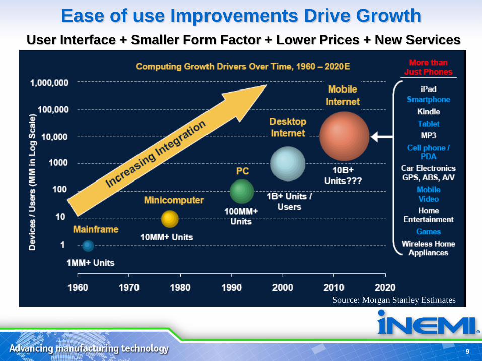
Ease of use Improvements Drive Growth
User Interface + Smaller Form Factor + Lower Prices + New Services
9
Source: Morgan Stanley Estimates

Consumer Segment drives Technology Changes
• Smart phones dominate unit volume growth for portable products, and the overall market volume growth is driving other areas:
– Increased focus on shrinking form factor and low power
– High level of integration (SoC, SiP)
– 3D packaging and Embedded Die market leaders
• Significant focus on sustainability, eco-design and recycling
• The MEMS/sensor technology for unleashing entertainment, medical, and security as well as perceptual computing
• Convergence of Entertainment, Computing, Communication drives integration
– The world of OS and applications and middleware challenges, will drive major shifts and consolidations to enable seamless computing and interoperability
– The pace of product enhancements is growing rapidly.
10

Consumer Market Needs driving
change in other segments
What does the Consumer want?
– Lower cost
– Higher performance
– Longer battery life
– Innovative features
– Connectivity (wireless)
– Smaller size
– Lighter weight
– Less heat generation
– Rapid availability
11
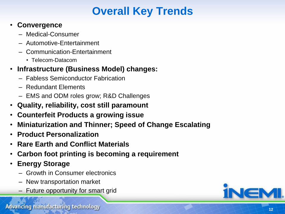
Overall Key Trends • Convergence
– Medical-Consumer
– Automotive-Entertainment
– Communication-Entertainment
• Telecom-Datacom
• Infrastructure (Business Model) changes:
– Fabless Semiconductor Fabrication
– Redundant Elements
– EMS and ODM roles grow; R&D Challenges
• Quality, reliability, cost still paramount
• Counterfeit Products a growing issue
• Miniaturization and Thinner; Speed of Change Escalating
• Product Personalization
• Rare Earth and Conflict Materials
• Carbon foot printing is becoming a requirement
• Energy Storage
– Growth in Consumer electronics
– New transportation market
– Future opportunity for smart grid
12
Automotive PEG
Chair: Jim Spall,
Delphi

• Business Issues
– Reduced North American volume in 2009 (worst year in 30 years)
– Western Europe sales tracking at a full-year rate near 14.7 million units
for 2009, 2010 volume could be reduced to 13.7 million units
– Japan sales declined to the lowest level in 38 years (2.9 million units)
– China exceeding the U.S. in auto output in 2009 (12 million units)
• Up 34 percent from a year earlier
– Increased Corporate Average Fuel Economy to 35.5 mpg by 2016
• Downsizing of engines and increased use of Gas Direct injection
• Increased use of turbo-charging
• Researchers project 14 million electrified vehicles annually by 2020
Situation Analysis - Business
Automotive Product Emulator Group
14
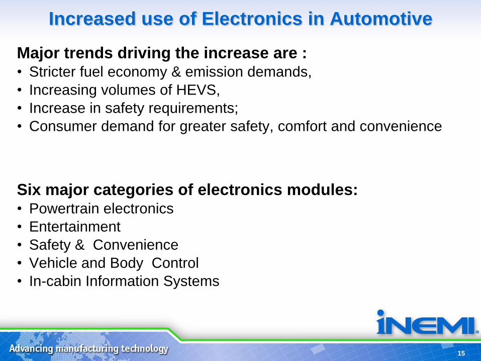
Major trends driving the increase are : • Stricter fuel economy & emission demands,
• Increasing volumes of HEVS,
• Increase in safety requirements;
• Consumer demand for greater safety, comfort and convenience
Six major categories of electronics modules: • Powertrain electronics
• Entertainment
• Safety & Convenience
• Vehicle and Body Control
• In-cabin Information Systems
Increased use of Electronics in Automotive
15

• High & low temperature extremes, vibration, shock, exposure to
dirt and contaminants, moisture, chemicals, radiation & gasses,
EMI/RFI shielding from internal & external noise & ESD
Unique Harsh Environment
16
Component Location
Passenger Compartment
Engine Compartment
On-Engine and On-Transmission
Wheel-Mounted Components
Operating Temperature(Baseplate)
-40 °C to 85 °C
-40 °C to 125 °C
-40 °C to 140 °C
-40 °C to 250 °C
Passenger Compartment
Wheel-Mounted Components
Engine Compartment
On Engine & On-Transmission
Salt
High Humidity
Rapid Change Temp.
Oxides of Nitrogen
High Vibration
Gasoline
Oil
Brake Fluid

• Technical Issues
– Shift to Hybrid Electric Vehicles (HEV), Plug-in Hybrid Electric Vehicles (PHEV), and Electric Vehicles (EV)
• Invention required to reach the battery cost target of $250/kWh
– Today‟s cost $1,000 -$1,200/kWh
• Key components that are in need include: power devices, bulk capacitors, inductors and transformers, cooling structures, motor drive microprocessors, high current connectors, current sensors, gate driver ICs, battery management ICs, bus bars, and enclosures.
– Increased use of MEMS in automotive
• Accelerometers
• Gyroscopes
• Pressure
• Air Flow
Situation Analysis - Technology
Automotive Product Emulator
17

Automotive MEMS; Growing Rapidly
Key Challenges are Long Life & Extreme Thermal
18
– 12.3 inch reconfigurable displays for the instrument panel
– LED lighting used internally and externally
– Connected Vehicle
• Key Drivers: cost, reliability, size
– Cost is still the key driver for automotive
– Reliability is a given in the automotive sector
– Size is a benefit because some vehicles having up to 100 electronic
controllers and space is limited
Situation Analysis (con’t.) - Technology
Automotive Product Emulator
19
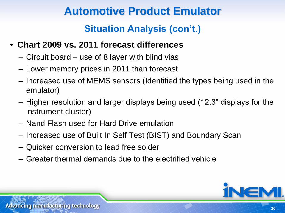
• Chart 2009 vs. 2011 forecast differences
– Circuit board – use of 8 layer with blind vias
– Lower memory prices in 2011 than forecast
– Increased use of MEMS sensors (Identified the types being used in the
emulator)
– Higher resolution and larger displays being used (12.3” displays for the
instrument cluster)
– Nand Flash used for Hard Drive emulation
– Increased use of Built In Self Test (BIST) and Boundary Scan
– Quicker conversion to lead free solder
– Greater thermal demands due to the electrified vehicle
Situation Analysis (con’t.)
Automotive Product Emulator
20
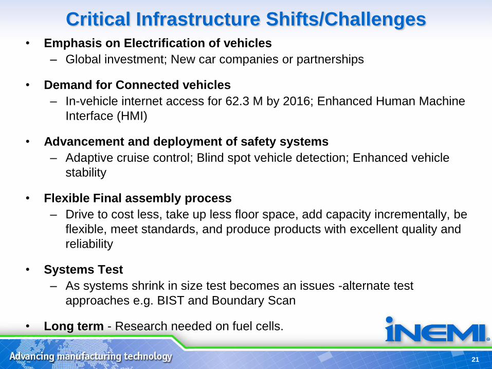
Critical Infrastructure Shifts/Challenges • Emphasis on Electrification of vehicles
– Global investment; New car companies or partnerships
• Demand for Connected vehicles
– In-vehicle internet access for 62.3 M by 2016; Enhanced Human Machine
Interface (HMI)
• Advancement and deployment of safety systems
– Adaptive cruise control; Blind spot vehicle detection; Enhanced vehicle
stability
• Flexible Final assembly process
– Drive to cost less, take up less floor space, add capacity incrementally, be
flexible, meet standards, and produce products with excellent quality and
reliability
• Systems Test
– As systems shrink in size test becomes an issues -alternate test
approaches e.g. BIST and Boundary Scan
• Long term - Research needed on fuel cells.
21
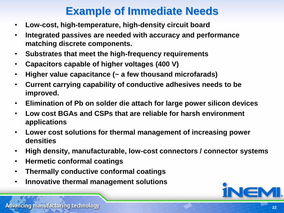
Example of Immediate Needs • Low-cost, high-temperature, high-density circuit board
• Integrated passives are needed with accuracy and performance
matching discrete components.
• Substrates that meet the high-frequency requirements
• Capacitors capable of higher voltages (400 V)
• Higher value capacitance (~ a few thousand microfarads)
• Current carrying capability of conductive adhesives needs to be
improved.
• Elimination of Pb on solder die attach for large power silicon devices
• Low cost BGAs and CSPs that are reliable for harsh environment
applications
• Lower cost solutions for thermal management of increasing power
densities
• High density, manufacturable, low-cost connectors / connector systems
• Hermetic conformal coatings
• Thermally conductive conformal coatings
• Innovative thermal management solutions
22

iNEMI 2011 Roadmap
Packaging & Component
Substrates TWG
Chairs:
Bill Bottoms, 3MTS
& Bill Chen, ASE
24
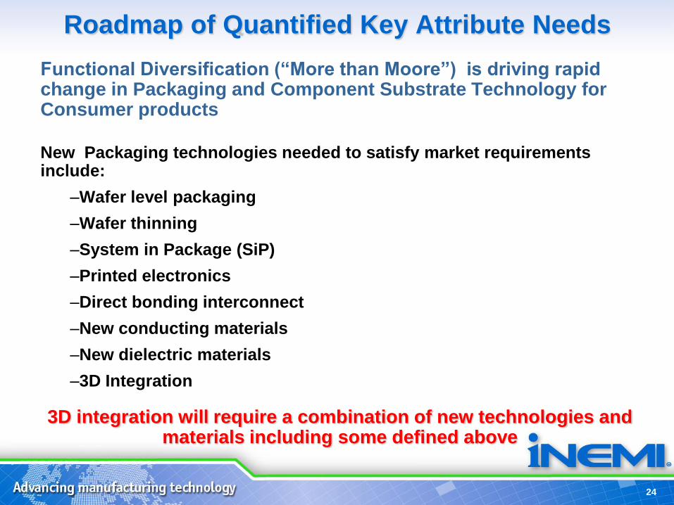
Roadmap of Quantified Key Attribute Needs
Functional Diversification (―More than Moore‖) is driving rapid change in Packaging and Component Substrate Technology for Consumer products
New Packaging technologies needed to satisfy market requirements include:
–Wafer level packaging
–Wafer thinning
–System in Package (SiP)
–Printed electronics
–Direct bonding interconnect
–New conducting materials
–New dielectric materials
–3D Integration
3D integration will require a combination of new technologies and materials including some defined above

Technologies Enabling 3D Integration
• Through Silicon Via – active wafer & interposers
• Two side wafer level Processes
– RDL and MicroBumping
• Embedded Components (active & passive)
• Wafer thinning & Handling
• Wafer to Wafer Bonding
• Die to Wafer Bonding
• Micro bump assembly
• Design Tools
• Micro fluidics Cooling
• Assembly of TSV die
• Test of TSV Die
Source: Phil Garrou, 2009
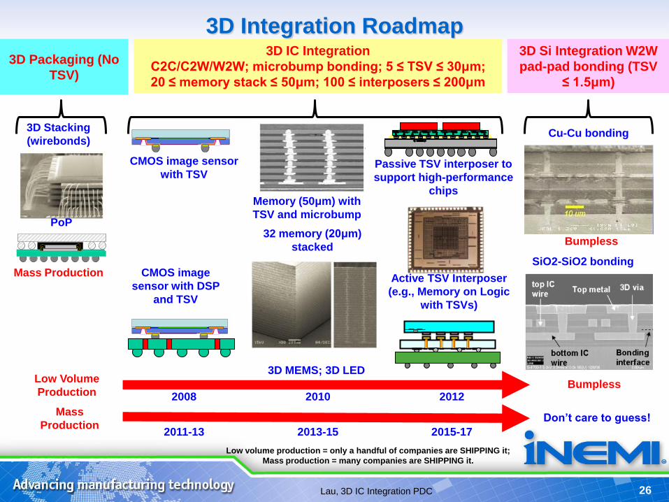
3D Packaging (No
TSV)
3D IC Integration
C2C/C2W/W2W; microbump bonding; 5 ≤ TSV ≤ 30μm;
20 ≤ memory stack ≤ 50μm; 100 ≤ interposers ≤ 200μm
3D Si Integration W2W
pad-pad bonding (TSV
≤ 1.5μm)
3D Stacking
(wirebonds)
PoP
CMOS image sensor
with TSV
Memory (50μm) with
TSV and microbump
Passive TSV interposer to
support high-performance
chips
CMOS image
sensor with DSP
and TSV
32 memory (20μm)
stacked
Active TSV Interposer
(e.g., Memory on Logic
with TSVs)
Mass Production
Low Volume
Production 2008 2010 2012
Don’t care to guess! Mass
Production 2011-13 2013-15 2015-17
Low volume production = only a handful of companies are SHIPPING it;
Mass production = many companies are SHIPPING it.
Cu-Cu bonding
SiO2-SiO2 bonding
3D MEMS; 3D LED
Lau, 3D IC Integration PDC
Bumpless
Bumpless
3D Integration Roadmap
26

LONG TERM (STRATEGIC ) PACKAGING GAPS Time Horizon: >5 Years
Key Projects Research
Area Details
Time
Horizon
Accelerated
package
Scaling
Mfg./Mat/
Design
• ↑ I/O density of package (e.g.: reduction in routing trace pitch)
• ↑Vertical interconnect density through via density increase,
PTH pitch and diameter scaling
• Improve electrical performance through tolerance control,
improved alternative Dielectric materials
• Tighter control in manufacturing process and cleanliness
2014 +
Flexible system
packaging
Mfg./Mat/
Design
• Cost effective thin organic packaging with thin die
• Standardized and fungible handling and HVM infrastructure
2011 +
Package to
Sustain High
current density
Mat/
Design
• Material systems and novel architectures to mitigate electro
migration risk with reduced bump pitch and shorter bump height
2012 +
3D packaging Mfg./Mat/
Design
• Through wafer via structure and via manufacturing/fill
processes
• Singulation of TSV wafers and, testing of individual dies in TSV
stack
• Alternative interconnect architectures beyond the C4 based
connection
2012 +
Pushing the Envelope
• All of these new technologies are moving very quickly.
• In today's world the effectiveness of an integrated supply
chain approach is key
• Multiple nodes on the supply chain covering all aspects of
design, materials, assembly, test, etc, etc
• Cooperative roadmap efforts of groups (such as, MIG,
iNEMI, IPC, TPCA and ITRS) are key to clarify timing and
needs
• There are many/many opportunities for collaborative R&D
28

Strategy Issues Graphics
Project Lead:
Project Co-Lead:
Tactics Milestones and/or Deliverables Plan Actual
Thrust Area:
Nov-11 TIG:
Goal:
Strategy Issues Graphics
Project Lead:
Project Co-Lead:
Tactics Milestones and/or Deliverables Plan Actual
Thrust Area:
TIG:
Goal: Understand key issues and concerns regarding reliability of fine-pitch Cu wire bonding for semiconductors.
• 2-phased project. The first phase will focus on collecting information from the industry regarding the key processing and reliability issues pertaining to Cu wire bonding. The second phase of the project will perform necessary experimental work in the areas defined by Phase 1.
• Copper bond wires are
increasingly being used for a wide
variety of components.
• Reliability needs to be collectively
assessed by the industry in a
quantitative manner.
• Standard reliability test methods
and durations for Au wire device
may not be sufficient for Cu. Peng Su, Cisco Systems, inc.
TBD
Phase 1 • 1. Industry Survey • 2. Existing Data Review • 3. DOE Plan for Phase 2 Phase 2 • 1. Finalize DOE • 2. Procure Materials • 3. Package Assembly • 4. Reliability Tests • 5. Failure Analysis • 6. Summary
Miniaturization
Packaging
Copper Wire Bonding Reliability Project
Initiative Launch Date
Project Inauguration - Two PS Signers
Conduct survey, analyze inputs
Plan DoE for phase 2
Phase 2 open for sign up
Sep-11
Mar-11 Dec-10
Jan-11 Nov-10
Sep-10 Sep-10
Mar-10 Mar-10
29
More information at: http://www.inemi.org/project-page/copper-wire-bonding-reliability

Environmentally Conscious
Electronics
Chairs: Ted Reichert, Intel
Jackie Adams, IBM

ECE Regulations Over Time; Growing Challenge
11/1/2011
Energy/Power
Substances
Climate change
The ICT supply chain is global. Products are designed & manufactured for the global market.
Inconsistent environmental regulations are challenges to continued innovation in ECE

Packaging
Compliance
Example of Environmental Compliance
Industry Responsibility – Highly Complex
DfE Manufacture Supply Chain Take-Back, Disposal,
& compliance
Design for
Environment
Material
Compliance
for WW RoHS
Design for
Recyclability
Design
For EuP
ECO-
Design
Disposal
Operations
Lead Free
reliability
RoHS /REACH
Compliant
Product
Information
Management
Proof Of
Compliance
Compliant
Processes
Identify Parts
& Assemblies
Alternative
technologies
Date of Mfg
(DoM)
Substance
Data mining
(IT)
Material
Declaration
(PCD)
Ship to
Restrictions
HazMat
Country Specific Legislation
Waste Water
and Energy
WEEE
Recovery
Treatment
Disposal
Confirmation
ELV
(Vehicles)
Material
Manifest
Destruction
Certificate
Audit
Non-
Conformance
Corrective
Action
Process
Categorize Identify Treatment Reporting/
Analysis Site
Inspection
Support
Changing
legislation
Transportation
Design
For PS
Design
verification
ESI Package
distribution
Retailer,
distributor
33
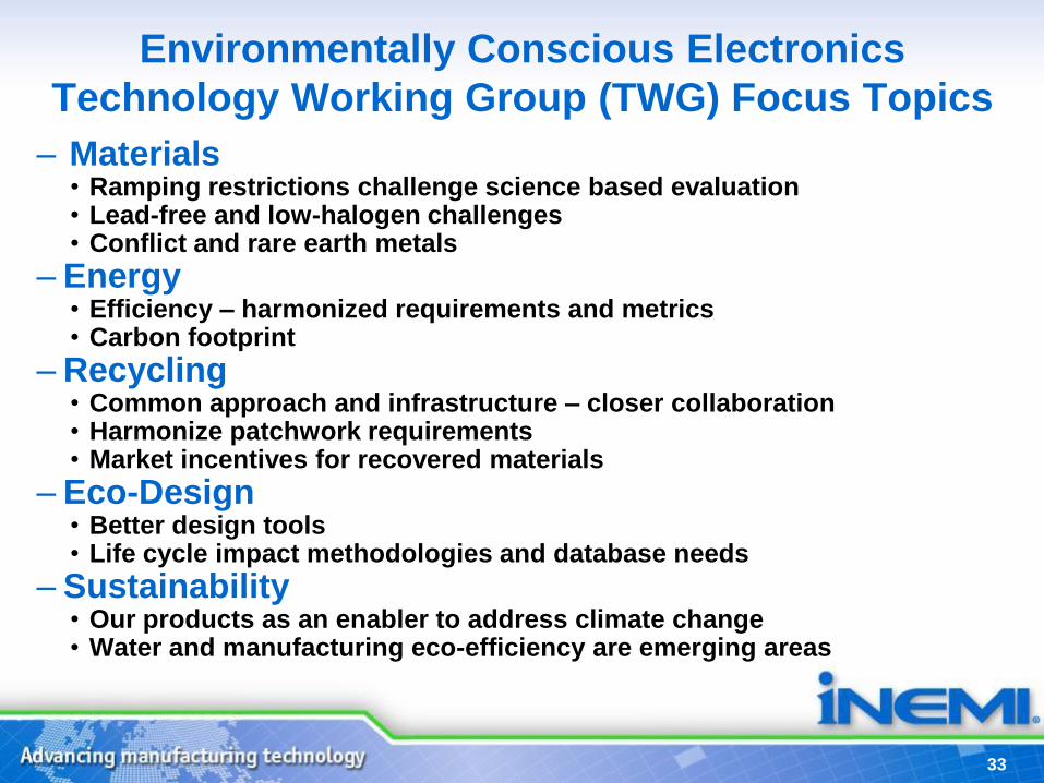
Environmentally Conscious Electronics
Technology Working Group (TWG) Focus Topics
– Materials • Ramping restrictions challenge science based evaluation • Lead-free and low-halogen challenges • Conflict and rare earth metals
– Energy • Efficiency – harmonized requirements and metrics • Carbon footprint
– Recycling • Common approach and infrastructure – closer collaboration • Harmonize patchwork requirements • Market incentives for recovered materials
– Eco-Design • Better design tools • Life cycle impact methodologies and database needs
– Sustainability • Our products as an enabler to address climate change • Water and manufacturing eco-efficiency are emerging areas

ECE Summary
• 2011 Issues
– New issues not in previous roadmap that will may impact product groups
• Rare earth and conflict metals
• Expanding list of restricted materials via global RoHS, REACH
• Carbon footprint
• Cross Cutting Issues
– Highlighted issues that are cross cutting with other TWGs
• Energy efficiency standards and technologies
• Transition to lead free and low halogen
• Additional restricted materials
• Standards for product data management
• Eco-design standards
34

35
All Materials are Phenolic Resin Based
MEB MEB Agilent
Layer Count / Thickness
18 Layer / 0.093‖ 24 Layer / 0.125‖ 20 Layer / 0.116
Drill Sizes 8mil / 10mil / 12mil 10mil / 12mil / 14 mil
Pitch 0.8mm / 1.0mm 0.8mm / 1.0mm
Reflow Temps 245C & 260C 245C 260
# Reflows 6x & 10x 6x & 10x 6x & 10x
Focus is on High Reliability (Server) Market Segment Application Space
PCB and PCBA components are HFR-free (Low-Halogen)
Board Thicknesses are 0.093‖ & 0.125‖ (MEB’s) & 0.116‖ (Agilent)
PCB Material are LF compatible, low / med loss and HVM capable
– 8 BFR-free Materials Identified with 1 Halogenated Material as Control
• All BFR-free TV’s have been completed and are being tested (estimated completion is end of Q4’11
iNEMI HFR-Free High-Reliability PCB Project

36
HFR-free Technology Leadership Project
Stephen Tisdale, Intel – Chair
HFR-Free Leadership Program
HFR-Free PCB Materials
Chair: John Davignon –
Intel
HFR-Free Signal Integrity
Chair: Stephen Hall - Intel
Co-Chair: David Senk - Cisco
Identify key thermo-mechanical performance
characteristics and determine if they are in the
critical path for the HFR-free PCB material
transition.
Ensure there is no degradation of electrical signals
in HFR-free PCB materials, base on investigation
of permittivity and loss as well as how they are
impacted by moisture absorption in new HFR-free
materials.

Strategy Issues Graphics
Project Lead:
Project Co-Lead:
Tactics Milestones and/or Deliverables Plan Actual
Thrust Area:
Nov-11 TIG:
Goal: Define the electrical signaling and PCB material property requirements as well as the associated test conditions
• Define the electrical signaling
• Define the material set parameters and test conditions for all relevant market segments
• Carry out the necessary testing of available materials from participating companies
• Publish a set of material guidelines
• Drive test conditions and material properties into supplier data sheets
Intel
• Identify candidate materials for evaluation
• Poll the supplier base, keying in on candidate
materials for market segment applications.
– Identify candidate HFR-free laminate materials
to allow interchangeability for standard
halogenated materials
Environment
Board Assembly
HFR-Free Signal Integrity Project
Review Prior Work
Identify Key Performance Characteristics
Test Vehicle Identification
Identification of Test Methods
Review Detailed Plans for Phase 2
Dec-09
Nov-09 Nov-09
Nov-09 Nov-09
Aug-09 Sep-09
Aug-09 Sep-09
3.4 3.5 3.6 3.7 3.8 3.9 4 4.1

38
Performance of HFR-free PCB vs FR4 HFR-free PCB materials on the market tend to have higher permittivity (Dk) values
than FR4
HFR-free Dk ~ 4.2 – 5.0 (1080)
FR4 Dk ~ 3.6-3.9 (1080)
3.4
3.6
3.8
4
4.2
4.4
4.6
4.8
5
15 17 19 21 23 25
Eye Area (ps-volts)
perm
itti
vit
y
Eye from lower limit of 1080 FR4
Eye from upper
range of HF
materials on the
market
37.5% margin degradation
vo
lta
ge
Time, ps
vo
lta
ge
Time, ps
Nominal 1080 FR4 permittivity
Simulation of three coupled 10” 50W microstrip lines;
dielectric thickness varied to maintain Zo; layout
rules similar to DDR buses (W/S/W=4/12/4)
Higher permittivity (Dk) reduces bus
performance
- Thicker layers for same Z0
increases crosstalk
- High crosstalk drives increased
trace separation & more layers
(increased cost)
HFR-free losses tend to be better than
FR4 & help compensate for crosstalk
for some buses

Roadmap Gap Analysis Leads to
Collaborative Approach
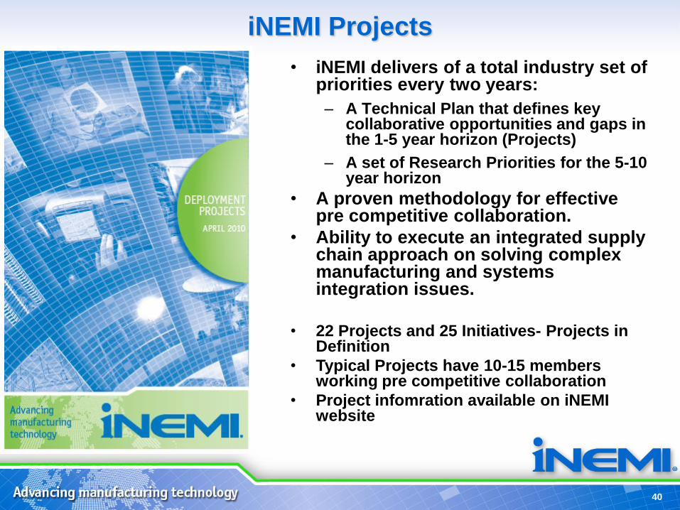
iNEMI Projects
40
• iNEMI delivers of a total industry set of priorities every two years:
– A Technical Plan that defines key collaborative opportunities and gaps in the 1-5 year horizon (Projects)
– A set of Research Priorities for the 5-10 year horizon
• A proven methodology for effective pre competitive collaboration.
• Ability to execute an integrated supply chain approach on solving complex manufacturing and systems integration issues.
• 22 Projects and 25 Initiatives- Projects in
Definition
• Typical Projects have 10-15 members working pre competitive collaboration
• Project infomration available on iNEMI website
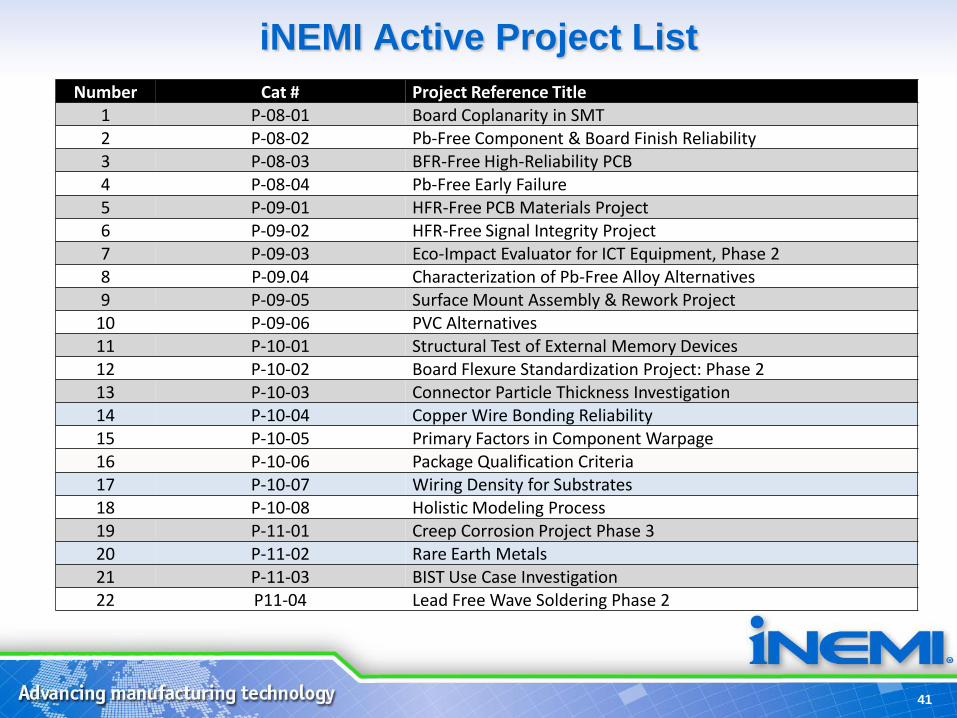
iNEMI Active Project List
41
Number Cat # Project Reference Title 1 P-08-01 Board Coplanarity in SMT 2 P-08-02 Pb-Free Component & Board Finish Reliability 3 P-08-03 BFR-Free High-Reliability PCB 4 P-08-04 Pb-Free Early Failure 5 P-09-01 HFR-Free PCB Materials Project 6 P-09-02 HFR-Free Signal Integrity Project 7 P-09-03 Eco-Impact Evaluator for ICT Equipment, Phase 2 8 P-09.04 Characterization of Pb-Free Alloy Alternatives 9 P-09-05 Surface Mount Assembly & Rework Project
10 P-09-06 PVC Alternatives 11 P-10-01 Structural Test of External Memory Devices 12 P-10-02 Board Flexure Standardization Project: Phase 2 13 P-10-03 Connector Particle Thickness Investigation 14 P-10-04 Copper Wire Bonding Reliability 15 P-10-05 Primary Factors in Component Warpage 16 P-10-06 Package Qualification Criteria 17 P-10-07 Wiring Density for Substrates 18 P-10-08 Holistic Modeling Process 19 P-11-01 Creep Corrosion Project Phase 3 20 P-11-02 Rare Earth Metals 21 P-11-03 BIST Use Case Investigation 22 P11-04 Lead Free Wave Soldering Phase 2
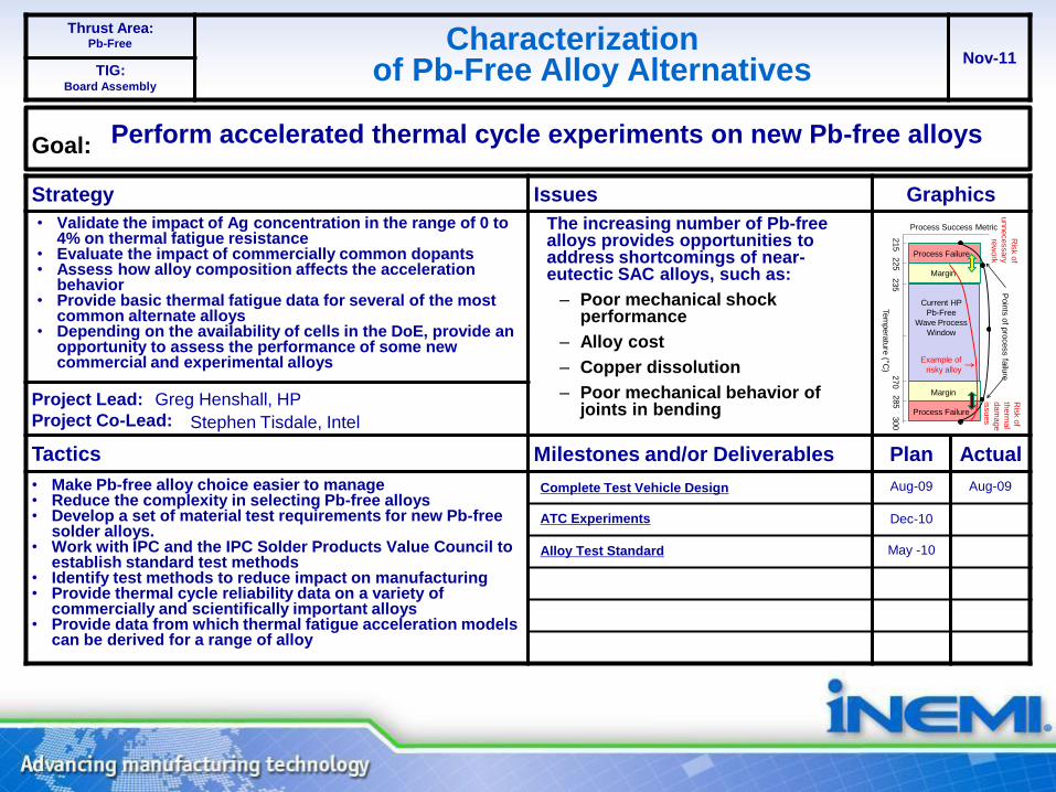
Strategy Issues Graphics
Project Lead:
Project Co-Lead:
Tactics Milestones and/or Deliverables Plan Actual
Thrust Area:
Nov-11 TIG:
Goal: Perform accelerated thermal cycle experiments on new Pb-free alloys
• Validate the impact of Ag concentration in the range of 0 to 4% on thermal fatigue resistance
• Evaluate the impact of commercially common dopants • Assess how alloy composition affects the acceleration
behavior • Provide basic thermal fatigue data for several of the most
common alternate alloys • Depending on the availability of cells in the DoE, provide an
opportunity to assess the performance of some new commercial and experimental alloys
The increasing number of Pb-free alloys provides opportunities to address shortcomings of near-eutectic SAC alloys, such as:
– Poor mechanical shock performance
– Alloy cost
– Copper dissolution
– Poor mechanical behavior of joints in bending
Greg Henshall, HP
Stephen Tisdale, Intel
• Make Pb-free alloy choice easier to manage • Reduce the complexity in selecting Pb-free alloys • Develop a set of material test requirements for new Pb-free
solder alloys. • Work with IPC and the IPC Solder Products Value Council to
establish standard test methods • Identify test methods to reduce impact on manufacturing • Provide thermal cycle reliability data on a variety of
commercially and scientifically important alloys • Provide data from which thermal fatigue acceleration models
can be derived for a range of alloy
Pb-Free
Board Assembly
Characterization of Pb-Free Alloy Alternatives
Complete Test Vehicle Design
ATC Experiments
Alloy Test Standard
May -10
Dec-10
Aug-09 Aug-09
Tem
pera
ture
( C)
270
235
300
285
215
225
Current HP
Pb-Free
Wave Process
Window
Margin
Margin
Process Failure
Process Failure
Poin
ts o
f pro
cess fa
ilure
Process Success Metric
Ris
k o
f
therm
al
dam
age
issues
Ris
k o
f
unnecessary
rew
ork
Example of
risky alloy

Strategy Issues Graphics
Project Lead:
Project Co-Lead:
Tactics Milestones and/or Deliverables Plan Actual
Thrust Area:
Nov-11 TIG:
Goal: Develop and promote the adoption of chip BIST at the board/system level
• Develop and promote the adoption of chip BIST at the board/system level
• Encourage IC vendors to provide standard chip BIST interfaces
• Encourage ATE/Instrument providers to develop products based existing related standards for BIST design
• Presently, there are no
Standard Chip level interfaces
or algorithms, for (BIST), which
limits the introduction of BIST
at board level test
Zoe Conroy, Cisco
Yang Yang, Huawei
• Phase 1 Survey of the industry on current BIST capabilities and future requirements - Complete
• Phase 2 BIST Use Case Investigation Project Project Sign-up Ends March 11, 2011
• Phase 3 ―Use Case‖ Function Classification Project
• Phase 4 Board Level Test Recommendations for Standardization of Component BIST - Project
Miniaturization
Test
Built in Self Test (BIST) Project - Phase 1
Plan Survey
Prepare Survey Logistics
Conduct Survey
Collect, Analyze and Share Data
Prepare Reports
“End of Project Webinar ( Phase 1) July-10 Mar-10
Jun-10 Feb-10
Jan-10 Jan-10
Dec-09 Dec-09
Dec-09 Dec-09
Nov-09 Nov-09
43

Strategy Issues Graphics
Project Lead:
Project Co-Lead:
Tactics Milestones and/or Deliverables Plan Actual
Thrust Area:
TIG:
Goal:
• Identify the important contributing factors based on component user and manufacturers’ experience and on observations from manufacturing operations, field engineering, and repair facilities.
• Develop recommendations for package structural design and material property selection to minimize warpage
• No clear understanding of the key contributors to warpage at the 1st and 2nd level assembly.
• Existing evaluation criteria for component warpage is not sufficient to prevent defects seen on High Volume SMT lines and in field.
• Component designers & manufacturers are not always aware of the severity of warpage induced defects, and more feedback is needed for these components.
Peng Su, Cisco Systems
Richard Coyle (Alcatel-Lucent)
• Phase 1 – Establish baseline of specific substrate
warpage factors – Plan industry survey to identify factors in
both manufacturing and field operations. – Collect and analyze results – Determine categories e.g. design, material
properties, no. of layers, core vs. coreless etc.
Miniaturization
Organic Pack. Substrates
Primary Factors in Component Warpage
Project
Project Launch Date
Analyse results
Develop categories
Investigate development of test board coupon
Project Final Report
4Q11
3Q11
3Q11
2Q11
2Q11
1Q11 1Q11
44
Develop set of primary parameters for materials, design and process and the working window to control component warpage through supply chain
Plan and conduct survey
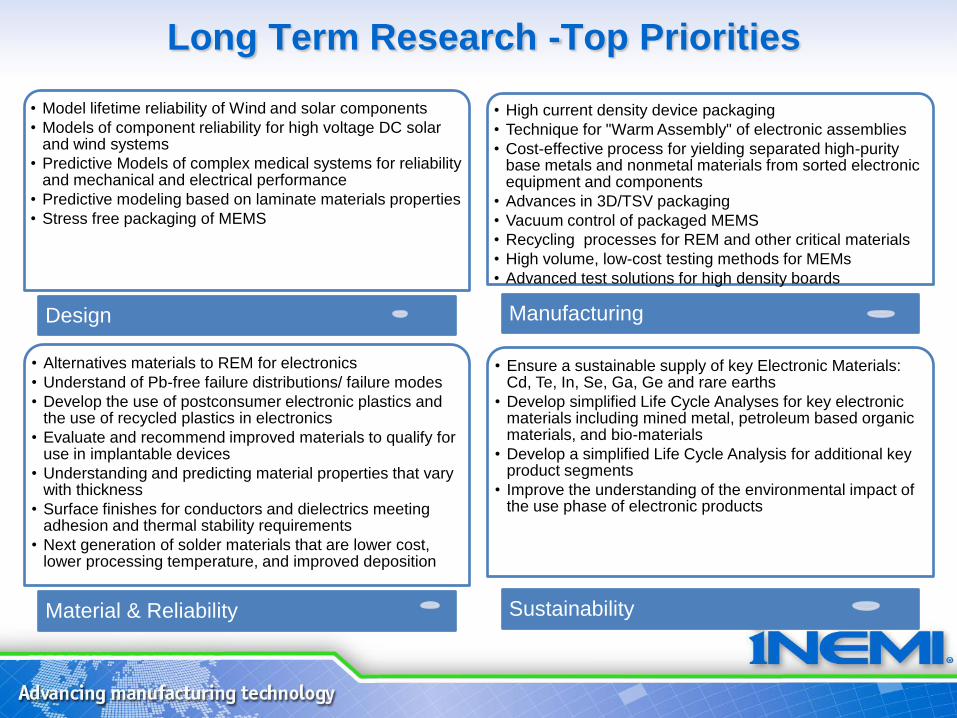
Long Term Research -Top Priorities
• Model lifetime reliability of Wind and solar components
• Models of component reliability for high voltage DC solar and wind systems
• Predictive Models of complex medical systems for reliability and mechanical and electrical performance
• Predictive modeling based on laminate materials properties
• Stress free packaging of MEMS
Design
• High current density device packaging
• Technique for "Warm Assembly" of electronic assemblies
• Cost-effective process for yielding separated high-purity base metals and nonmetal materials from sorted electronic equipment and components
• Advances in 3D/TSV packaging
• Vacuum control of packaged MEMS
• Recycling processes for REM and other critical materials
• High volume, low-cost testing methods for MEMs
• Advanced test solutions for high density boards
Manufacturing
• Alternatives materials to REM for electronics
• Understand of Pb-free failure distributions/ failure modes
• Develop the use of postconsumer electronic plastics and the use of recycled plastics in electronics
• Evaluate and recommend improved materials to qualify for use in implantable devices
• Understanding and predicting material properties that vary with thickness
• Surface finishes for conductors and dielectrics meeting adhesion and thermal stability requirements
• Next generation of solder materials that are lower cost, lower processing temperature, and improved deposition
Material & Reliability
• Ensure a sustainable supply of key Electronic Materials: Cd, Te, In, Se, Ga, Ge and rare earths
• Develop simplified Life Cycle Analyses for key electronic materials including mined metal, petroleum based organic materials, and bio-materials
• Develop a simplified Life Cycle Analysis for additional key product segments
• Improve the understanding of the environmental impact of the use phase of electronic products
Sustainability

Summary
• Convergence of markets is gaining speed
– Medical-Consumer
– Automotive-Entertainment
– Communication-Entertainment
• Growth of MEMs applications will escalate – consumer, automotive, medical
• Rapid evolution of 3D packaging led by consumer markets
• Proactive Rare Earth Metals and Conflict Materials Management are required
• Trends on environmental regulation growth globally
• Energy Storage criticality increasing:
– Miniaturization & Battery life in Consumer & Medical
– Improvements in Automotive Affects the total supply chain
– Growing opportunity for smart grid, solar, wind system storage
46
Collaborative Approach
• Technology continues to move at a faster rate of change
• Driven in many cases by short life cycle, low cost high volume product
• Many of these ―cool new things‖ don’t transpose well or quickly to high
reliability markets such as automotive, aerospace, medical, or high end
networking
• Key deliverables from iNEMI are the Roadmap. From this the 2011
Technical Plan (available only to members) and the 2011 Research
Priorities are developed.
• Effective usage and coordination behind both these documents will be key
to continued industry progress and growth
• Work Starts on the 2013 Roadmap Development in Sept.
We encourage you to contribute!
It is a global full supply chain industry wide look at future
technology metrics & gaps
47