Embed Size (px)
Citation preview
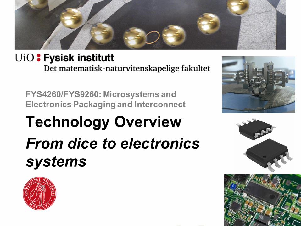
FYS4260/FYS9260: Microsystems and Electronics Packaging and Interconnect
Technology Overview From dice to electronics systems
Topics
• Introduce main electronics packaging technologies (more details later in the term!) – Circuit board technologies – Mounting technologies – Kahoot test at the end of the lecture!
• Related reading:
– Halbo&Ohlckers Chapter 2
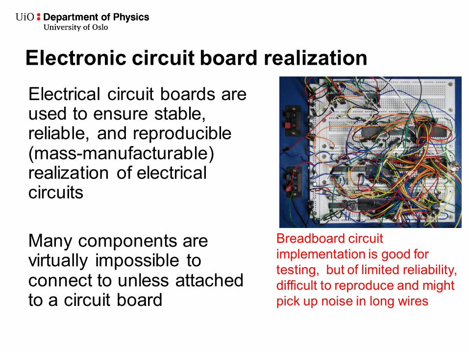
Electronic circuit board realization Electrical circuit boards are used to ensure stable, reliable, and reproducible (mass-manufacturable) realization of electrical circuits Many components are virtually impossible to connect to unless attached to a circuit board
Breadboard circuit implementation is good for testing, but of limited reliability, difficult to reproduce and might pick up noise in long wires
Choosing the right circuit board technology depend on system requirements • Performance requirements
– Clock speed, accuracy, power consumption, weight, size et cetera
• Operating environment • Required reliability and lifetime of product • Production volume • Need of repairability • Acceptable cost • Engineer's approach: Good enough is enough! It is
an art not to overdo a design!
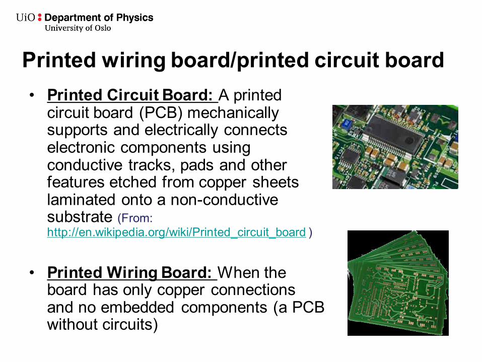
Printed wiring board/printed circuit board • Printed Circuit Board: A printed
circuit board (PCB) mechanically supports and electrically connects electronic components using conductive tracks, pads and other features etched from copper sheets laminated onto a non-conductive substrate (From: http://en.wikipedia.org/wiki/Printed_circuit_board )
• Printed Wiring Board: When the
board has only copper connections and no embedded components (a PCB without circuits)
Printed wiring board/printed circuit board
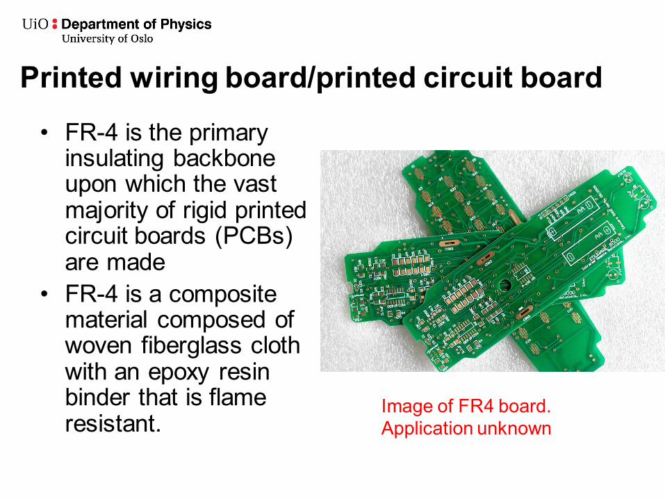
• FR-4 is the primary insulating backbone upon which the vast majority of rigid printed circuit boards (PCBs) are made
• FR-4 is a composite material composed of woven fiberglass cloth with an epoxy resin binder that is flame resistant.
Image of FR4 board. Application unknown
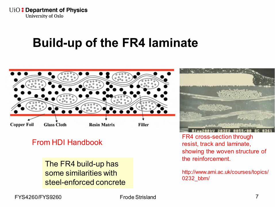
Build-up of the FR4 laminate
From HDI Handbook
FYS4260/FYS9260 Frode Strisland 7
FR4 cross-section through resist, track and laminate, showing the woven structure of the reinforcement. http://www.ami.ac.uk/courses/topics/0232_bbm/
The FR4 build-up has some similarities with steel-enforced concrete
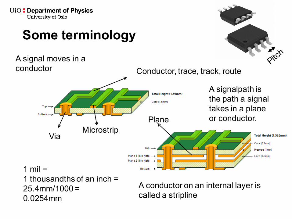
Some terminology
Conductor, trace, track, route
Via
Plane Microstrip
A conductor on an internal layer is called a stripline
1 mil = 1 thousandths of an inch = 25.4mm/1000 = 0.0254mm
A signal moves in a conductor
A signalpath is the path a signal takes in a plane or conductor.
FYS4260/FYS9260 Frode Strisland 9
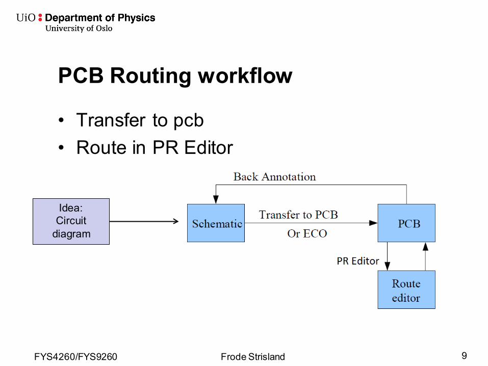
• Transfer to pcb • Route in PR Editor
PCB Routing workflow
Idea: Circuit
diagram
FYS4260/FYS9260 Frode Strisland 10
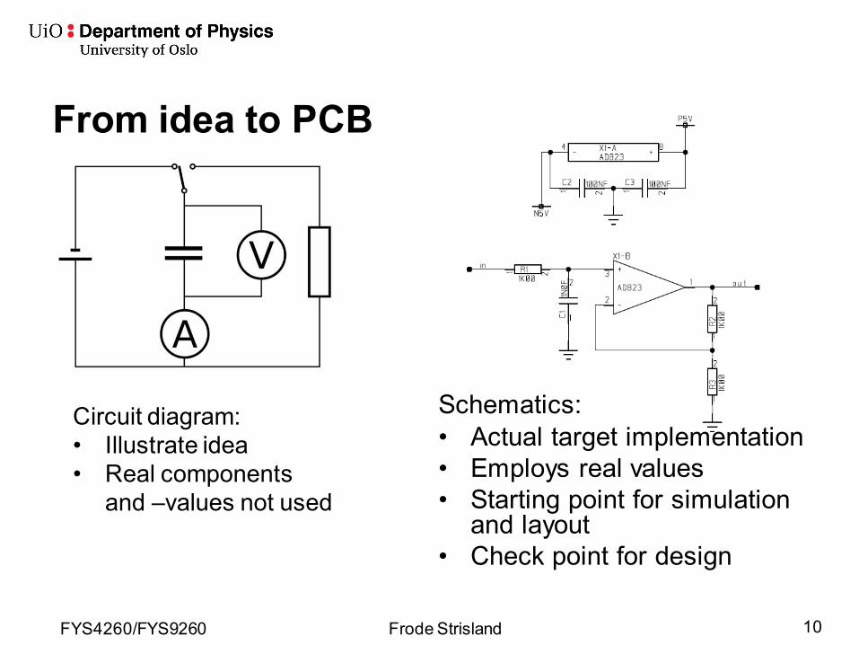
Circuit diagram: • Illustrate idea • Real components
and –values not used
From idea to PCB
Schematics: • Actual target implementation • Employs real values • Starting point for simulation
and layout • Check point for design
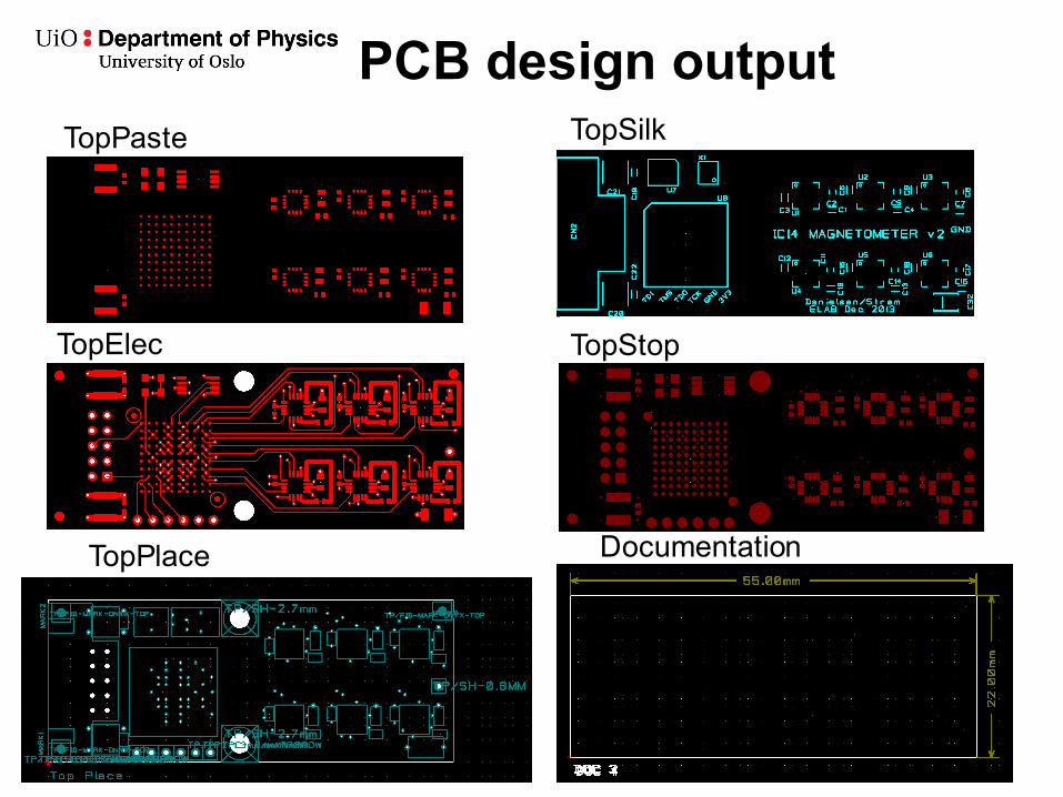
TopPaste TopSilk
TopElec TopStop
Documentation TopPlace
PCB design output
FYS4260/FYS9260 Frode Strisland 12
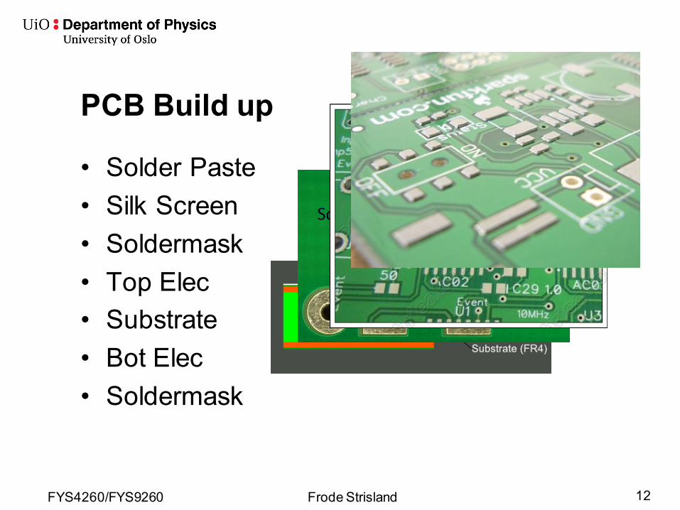
• Solder Paste • Silk Screen • Soldermask • Top Elec • Substrate • Bot Elec • Soldermask
PCB Build up
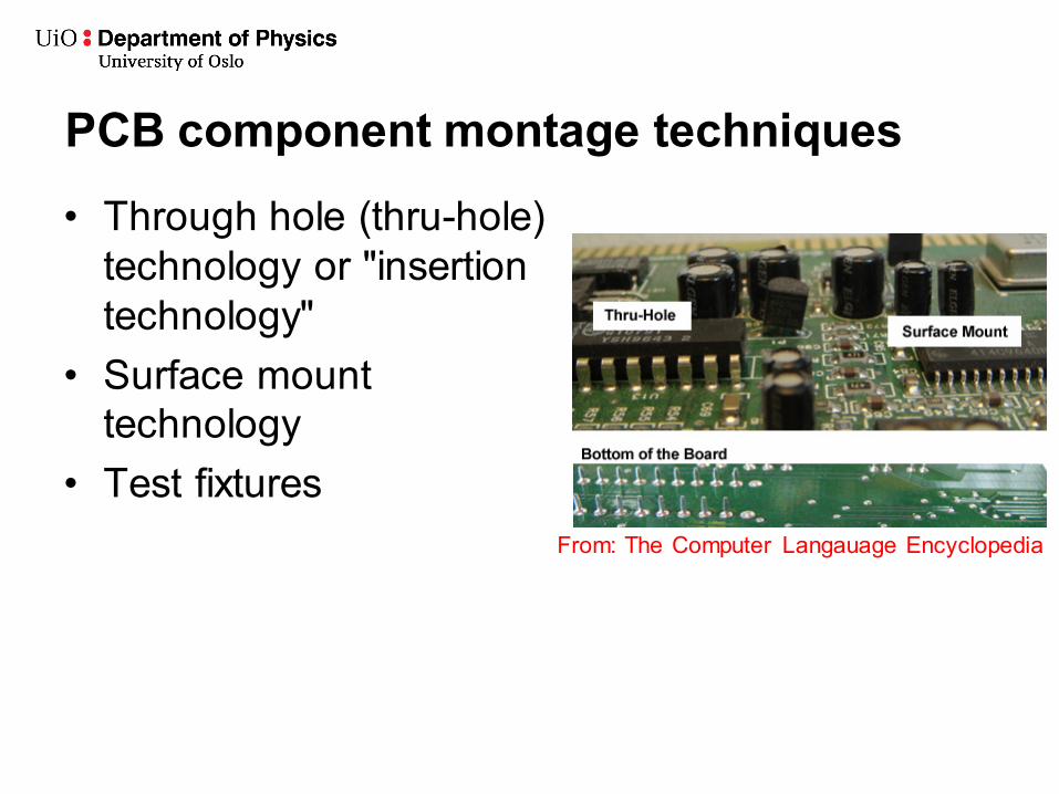
PCB component montage techniques
• Through hole (thru-hole) technology or "insertion technology"
• Surface mount technology
• Test fixtures From: The Computer Langauage Encyclopedia
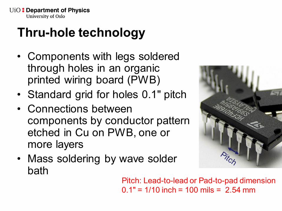
Thru-hole technology
• Components with legs soldered through holes in an organic printed wiring board (PWB)
• Standard grid for holes 0.1" pitch • Connections between
components by conductor pattern etched in Cu on PWB, one or more layers
• Mass soldering by wave solder bath Pitch: Lead-to-lead or Pad-to-pad dimension
0.1" = 1/10 inch = 100 mils = 2.54 mm
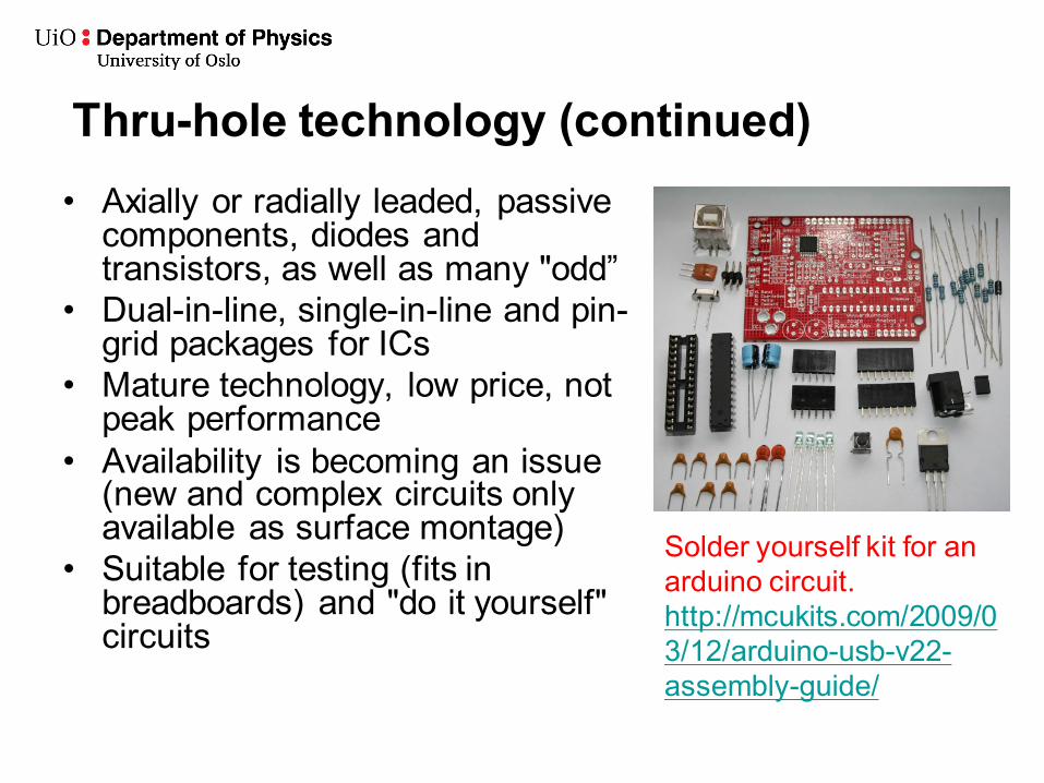
Thru-hole technology (continued) • Axially or radially leaded, passive
components, diodes and transistors, as well as many "odd”
• Dual-in-line, single-in-line and pin-grid packages for ICs
• Mature technology, low price, not peak performance
• Availability is becoming an issue (new and complex circuits only available as surface montage)
• Suitable for testing (fits in breadboards) and "do it yourself" circuits
Solder yourself kit for an arduino circuit. http://mcukits.com/2009/03/12/arduino-usb-v22-assembly-guide/
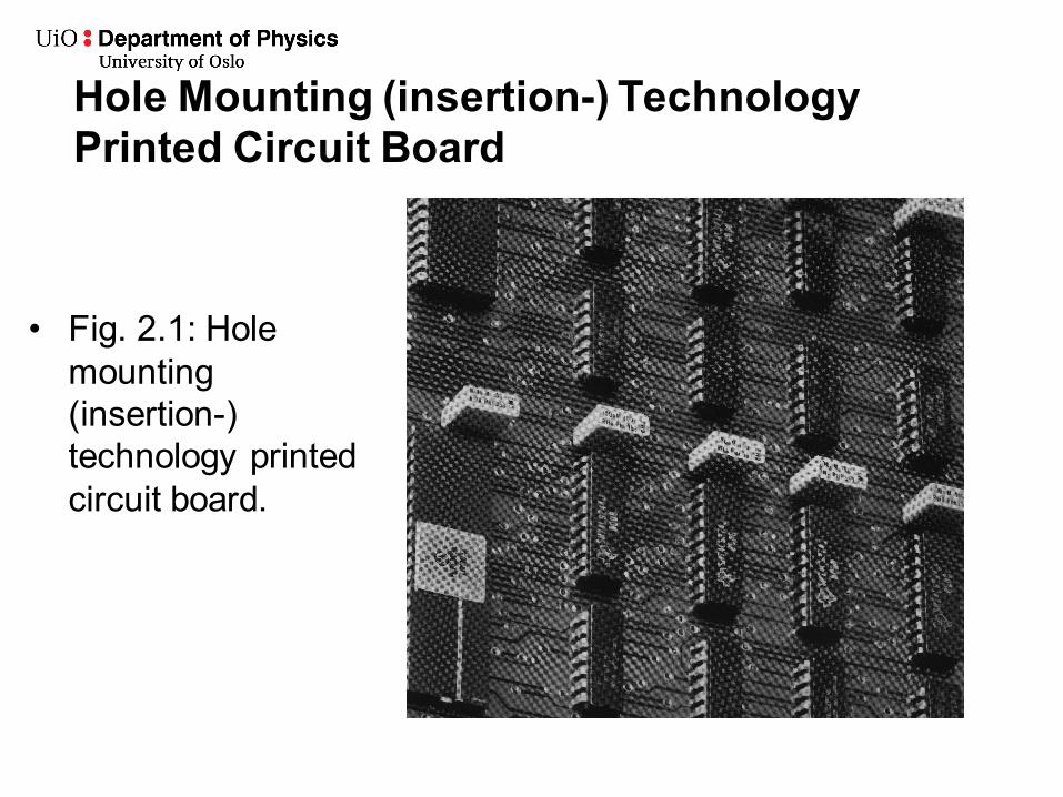
Hole Mounting (insertion-) Technology Printed Circuit Board
• Fig. 2.1: Hole mounting (insertion-) technology printed circuit board.
Surface Mount Technology
FYS4260/FYS9260 Frode Strisland 17
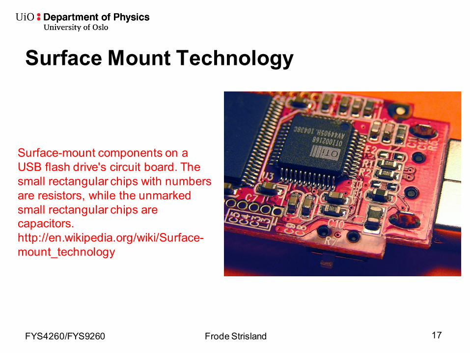
Surface-mount components on a USB flash drive's circuit board. The small rectangular chips with numbers are resistors, while the unmarked small rectangular chips are capacitors. http://en.wikipedia.org/wiki/Surface-mount_technology
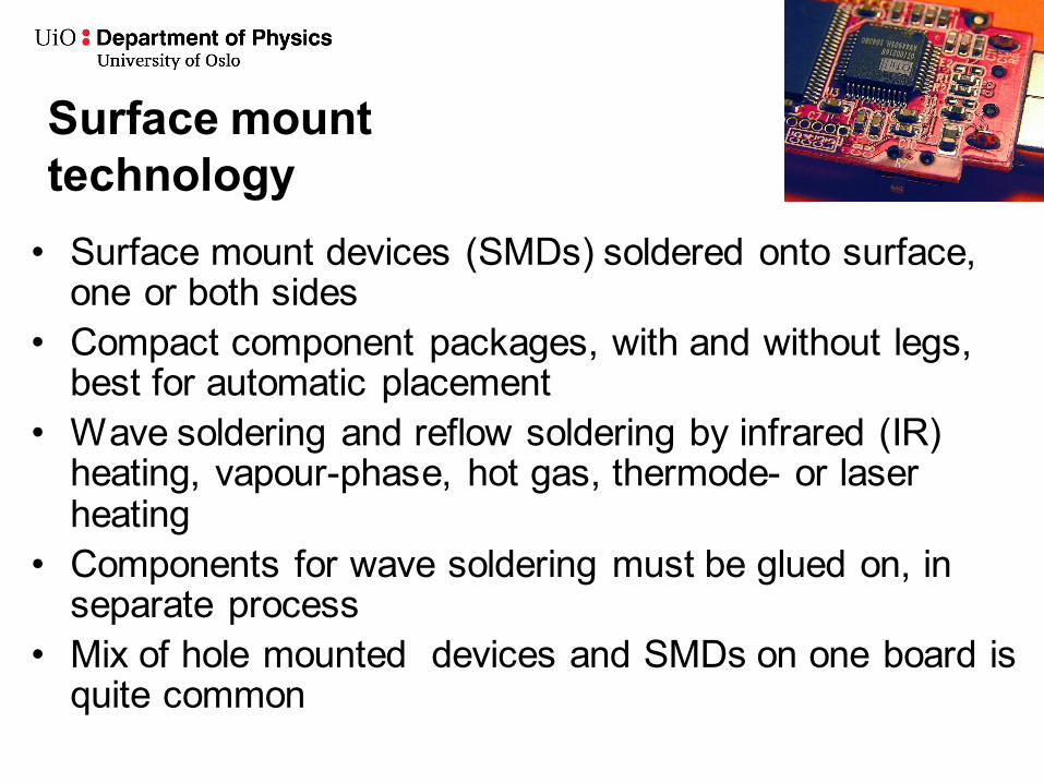
Surface mount technology
• Surface mount devices (SMDs) soldered onto surface, one or both sides
• Compact component packages, with and without legs, best for automatic placement
• Wave soldering and reflow soldering by infrared (IR) heating, vapour-phase, hot gas, thermode- or laser heating
• Components for wave soldering must be glued on, in separate process
• Mix of hole mounted devices and SMDs on one board is quite common
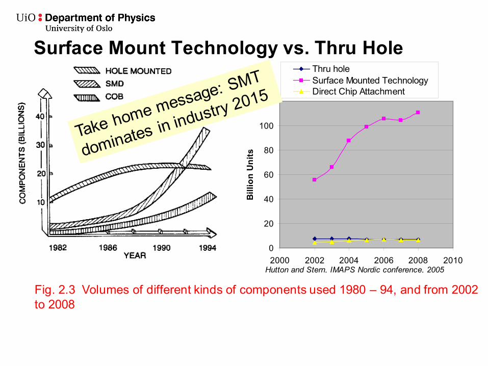
Surface Mount Technology vs. Thru Hole
Fig. 2.3 Volumes of different kinds of components used 1980 – 94, and from 2002 to 2008
Hutton and Stern, IMAPS Nordic conference, 2005
0
20
40
60
80
100
120
2000 2002 2004 2006 2008 2010B
illio
n U
nits
Thru holeSurface Mounted TechnologyDirect Chip Attachment
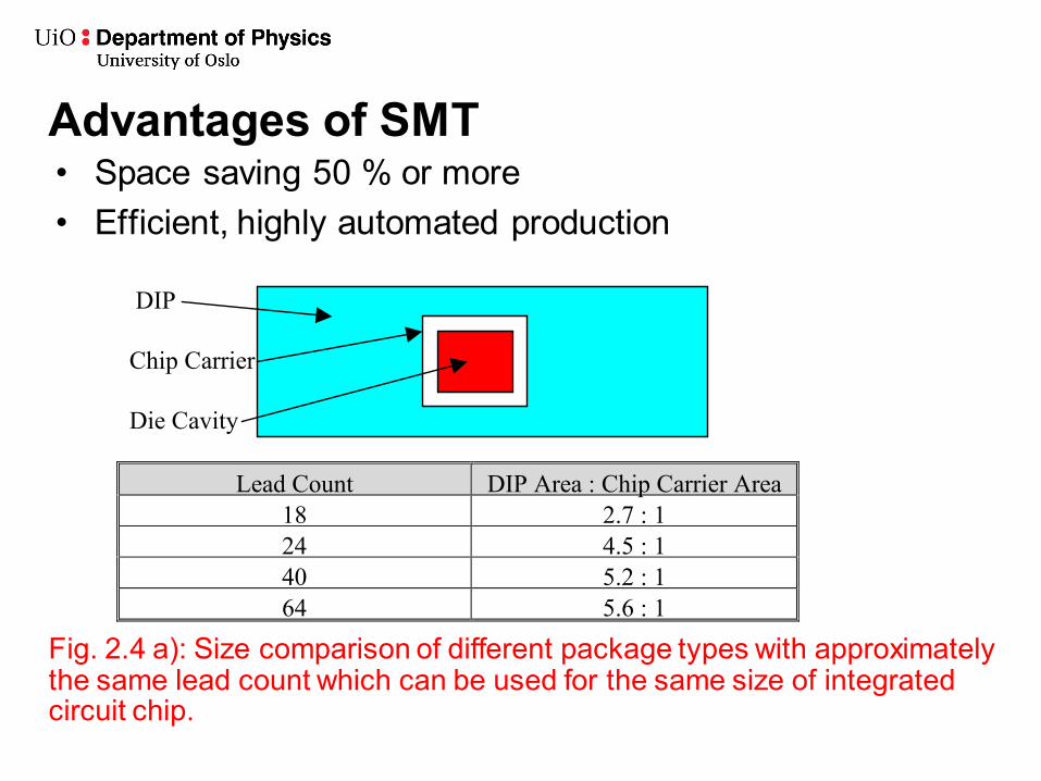
Advantages of SMT • Space saving 50 % or more • Efficient, highly automated production
Fig. 2.4 a): Size comparison of different package types with approximately the same lead count which can be used for the same size of integrated circuit chip.
DIP
Chip Carrier
Die Cavity
Lead Count DIP Area : Chip Carrier Area18 2.7 : 124 4.5 : 140 5.2 : 164 5.6 : 1
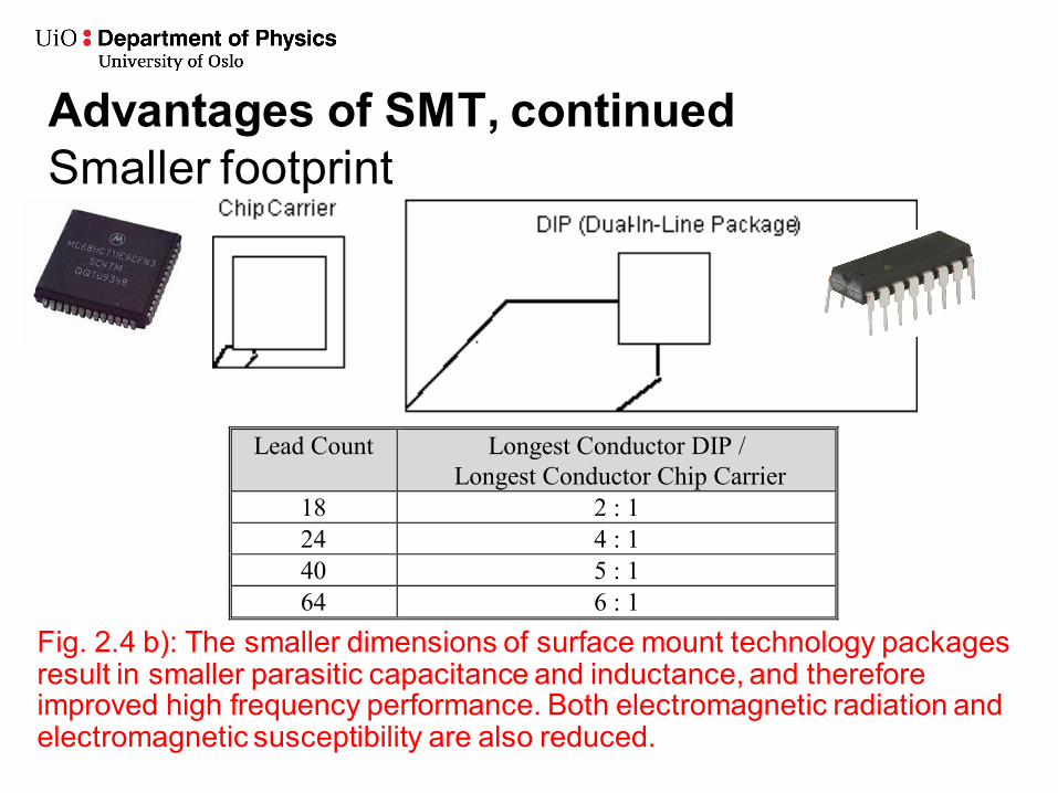
Advantages of SMT, continued Smaller footprint
Fig. 2.4 b): The smaller dimensions of surface mount technology packages result in smaller parasitic capacitance and inductance, and therefore improved high frequency performance. Both electromagnetic radiation and electromagnetic susceptibility are also reduced.
Lead Count Longest Conductor DIP /
Longest Conductor Chip Carrier 18 2 : 1 24 4 : 1 40 5 : 1 64 6 : 1
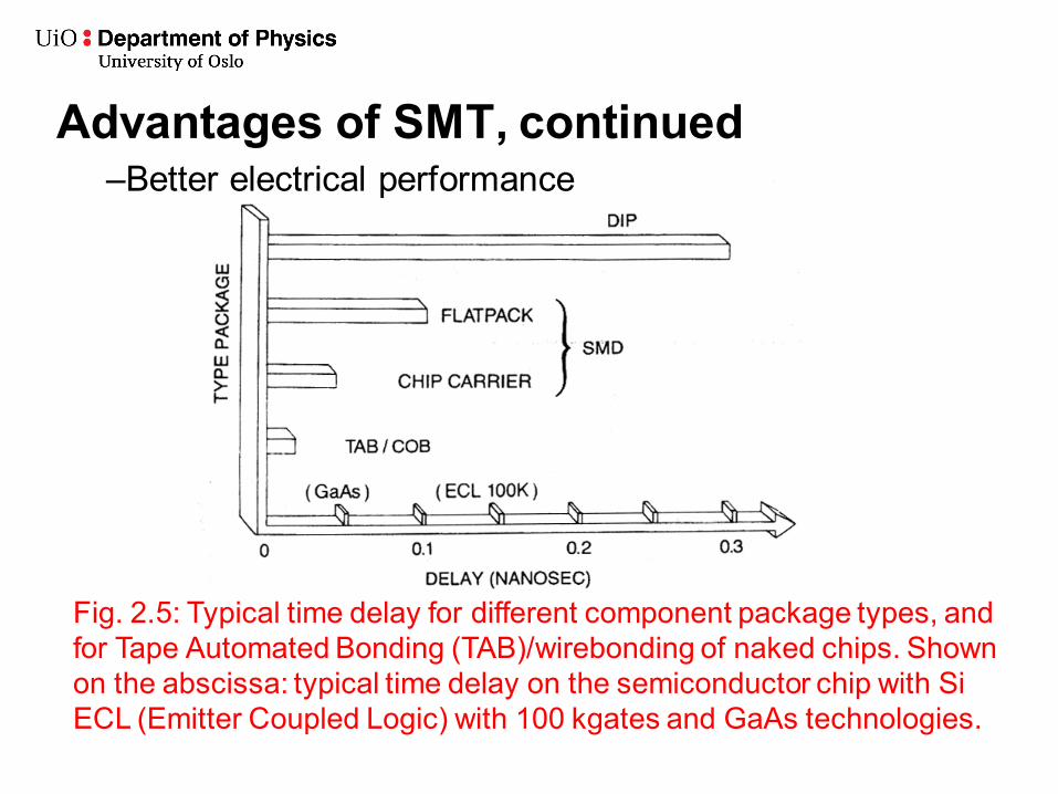
Advantages of SMT, continued –Better electrical performance
Fig. 2.5: Typical time delay for different component package types, and for Tape Automated Bonding (TAB)/wirebonding of naked chips. Shown on the abscissa: typical time delay on the semiconductor chip with Si ECL (Emitter Coupled Logic) with 100 kgates and GaAs technologies.
Electronic Pack….. Chapter 2 Slide 23
Advantages of SMT, continued • Better reliability in some cases • Lower component price in many cases • Advanced components require SMT- many
components are not available for thru-hole mounting
• SMT is taking over for hole mounting

Disadvantages of SMT
• Thermal mismatch component/substrate may reduce reliability or require more expensive materials
• More complex and demanding production process
• More demanding design and testing • Higher component density requires more
efficient cooling • Possibility of overheating components in the
soldering processes may give reduced reliability
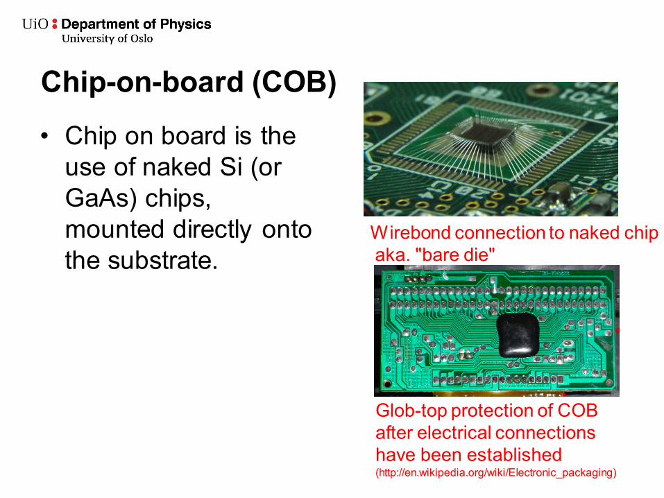
Chip-on-board (COB)
• Chip on board is the use of naked Si (or GaAs) chips, mounted directly onto the substrate.
Wirebond connection to naked chip aka. "bare die"
Glob-top protection of COB after electrical connections have been established (http://en.wikipedia.org/wiki/Electronic_packaging)
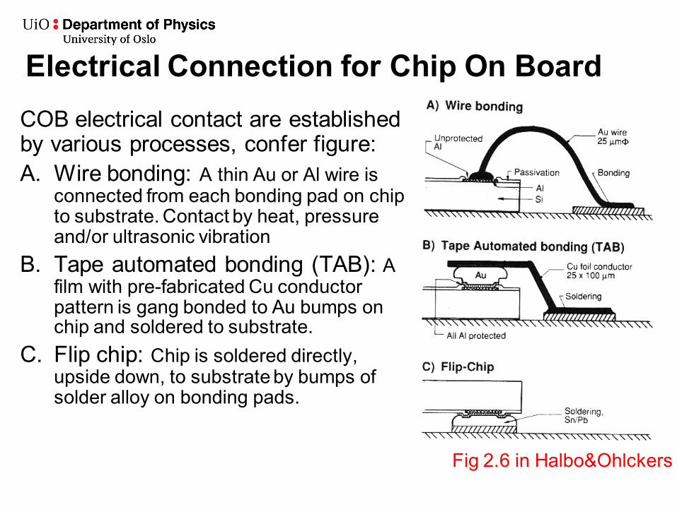
Electrical Connection for Chip On Board COB electrical contact are established by various processes, confer figure: A. Wire bonding: A thin Au or Al wire is
connected from each bonding pad on chip to substrate. Contact by heat, pressure and/or ultrasonic vibration
B. Tape automated bonding (TAB): A film with pre-fabricated Cu conductor pattern is gang bonded to Au bumps on chip and soldered to substrate.
C. Flip chip: Chip is soldered directly, upside down, to substrate by bumps of solder alloy on bonding pads.
Fig 2.6 in Halbo&Ohlckers
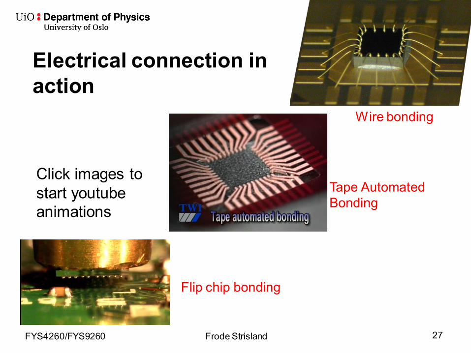
Electrical connection in action
Click images to start youtube animations
FYS4260/FYS9260 Frode Strisland 27
Wire bonding
Tape Automated Bonding
Flip chip bonding
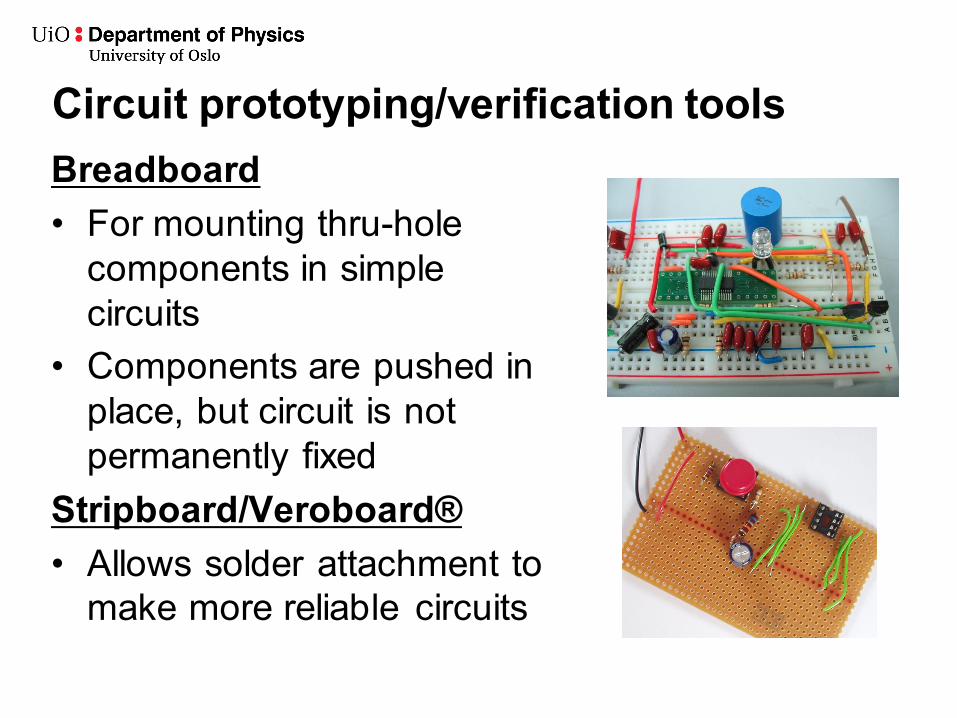
Circuit prototyping/verification tools Breadboard • For mounting thru-hole
components in simple circuits
• Components are pushed in place, but circuit is not permanently fixed
Stripboard/Veroboard® • Allows solder attachment to
make more reliable circuits
Limitations to circuit prototyping/verification tools: • Not suitable for high frequency (long wires
susceptible to noise) • Require thru-hole components • Mounting errors are possible and difficult to spot
(colour coding of wires and a structured layout helps avoiding help)
• For sensitive components, consider a dedicated test PCB realization of critical circuit design!
FYS4260/FYS9260 Frode Strisland 29
Halbo and Ohlckers book
• Still possible to buy at the physics expedition. • Bring cash – accurate amount: 150 Kr
Additional course material: http://tid.uio.no/kurs/fys4260/
• Electronic version of book • Past exams
FYS4260/FYS9260 Frode Strisland 30
On mandatory lab project
• 18 students registred • 4 have stated which project work they want
to do.
• The rest: Make up your mind, and report your decision to [email protected] ASAP!

Thick Film Hybrid Technology
• High temperature thick film: – Screen printing of
conducting, resistive and insulating materials in paste form onto ceramic substrate, in many layers.
Thick film hybrid circuit
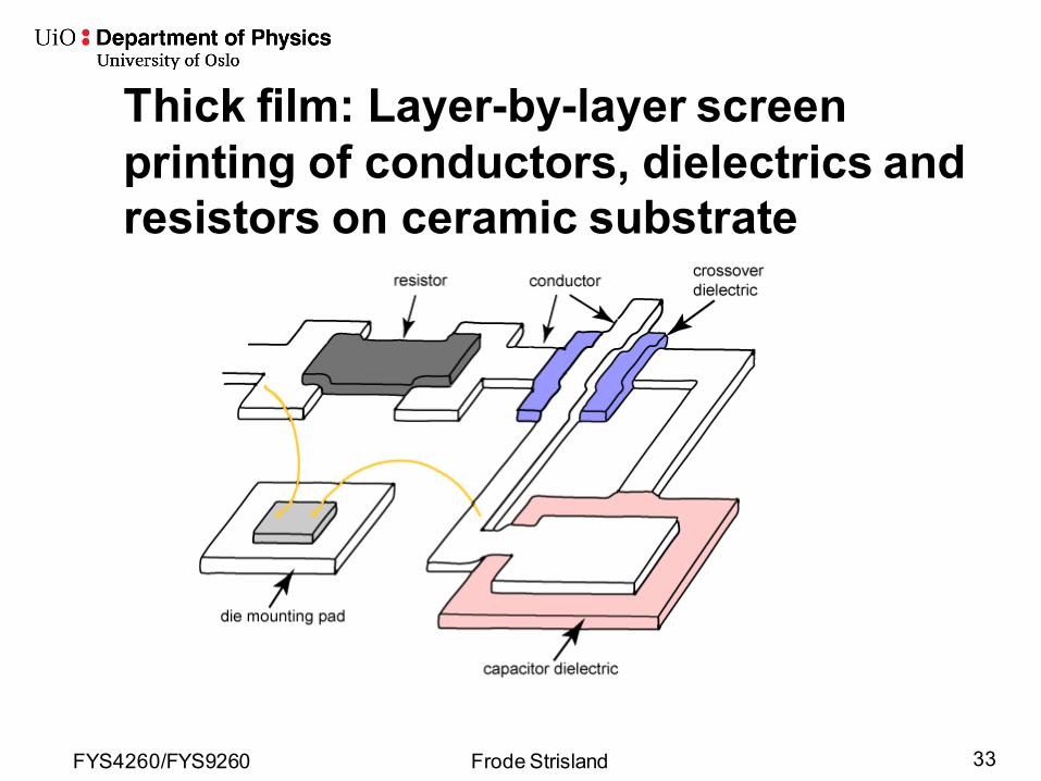
FYS4260/FYS9260 Frode Strisland 33
Thick film: Layer-by-layer screen printing of conductors, dielectrics and resistors on ceramic substrate
FYS4260/FYS9260 Frode Strisland 34
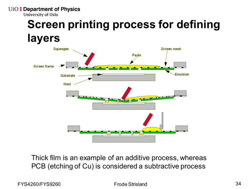
Screen printing process for defining layers
Thick film is an example of an additive process, whereas PCB (etching of Cu) is considered a subtractive process
Thick Film Hybrid Technology, continued
• Heat treatment ("firing") to stabilize, T≈ 800 degrees C
• Conductor paste consists of metal particles in glass matrix that melts in firing process
• Resistor paste contains resistive metal oxides, and dielectrics contain only glass matrix.
• High reliability, compact, may be more costly than PCB technology
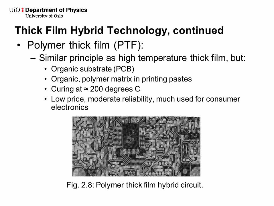
Thick Film Hybrid Technology, continued • Polymer thick film (PTF):
– Similar principle as high temperature thick film, but: • Organic substrate (PCB) • Organic, polymer matrix in printing pastes • Curing at ≈ 200 degrees C • Low price, moderate reliability, much used for consumer
electronics
Fig. 2.8: Polymer thick film hybrid circuit.
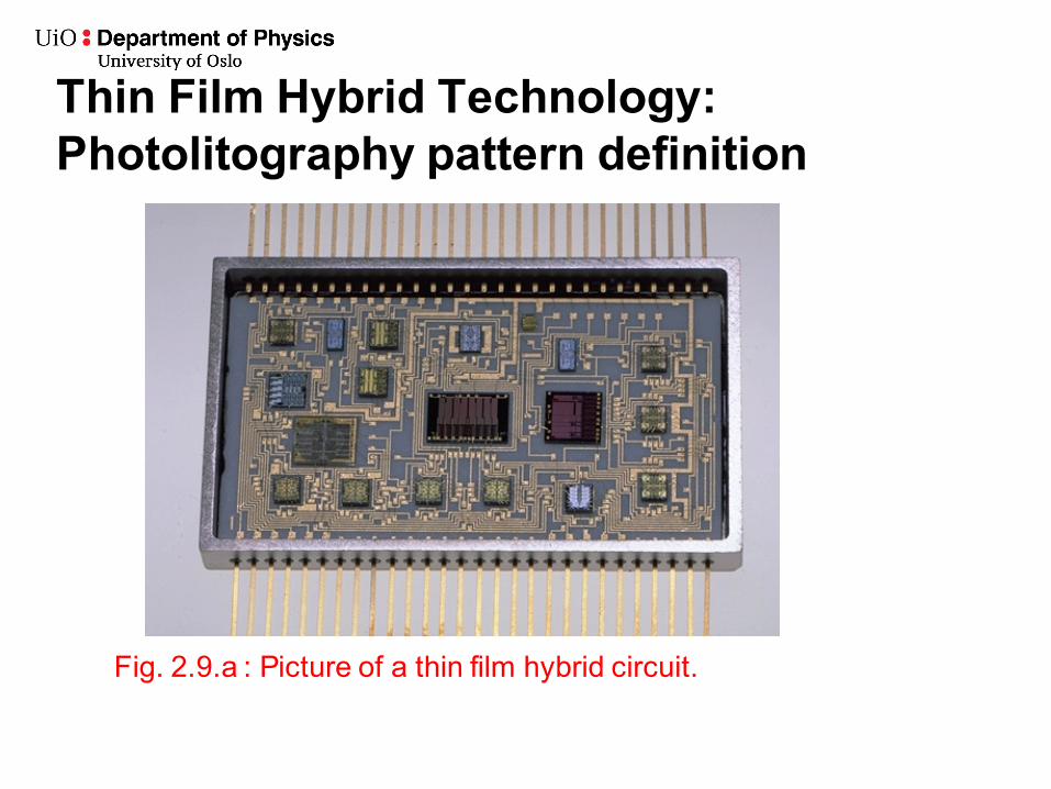
Thin Film Hybrid Technology: Photolitography pattern definition
Fig. 2.9.a : Picture of a thin film hybrid circuit.
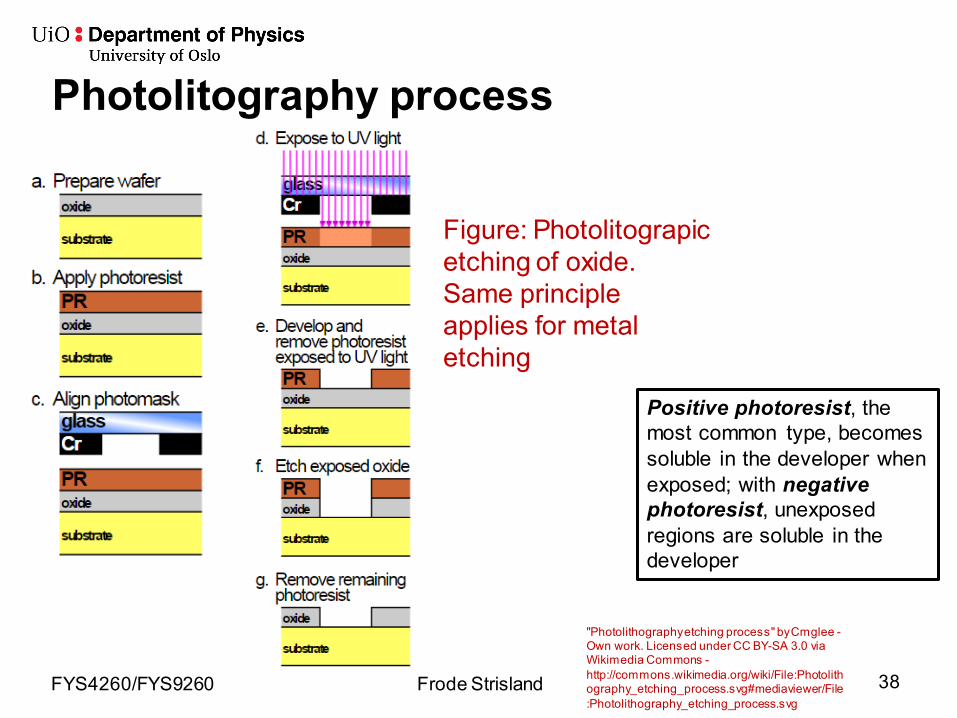
Photolitography process
FYS4260/FYS9260 Frode Strisland 38
"Photolithography etching process" by Cmglee - Own work. Licensed under CC BY-SA 3.0 via Wikimedia Commons - http://commons.wikimedia.org/wiki/File:Photolithography_etching_process.svg#mediaviewer/File:Photolithography_etching_process.svg
Positive photoresist, the most common type, becomes soluble in the developer when exposed; with negative photoresist, unexposed regions are soluble in the developer
Figure: Photolitograpic etching of oxide. Same principle applies for metal etching
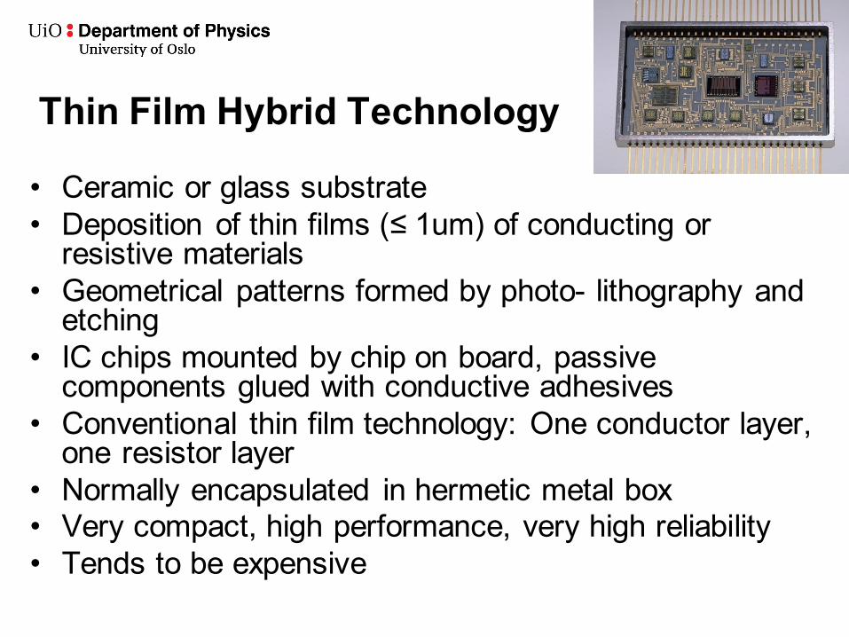
Thin Film Hybrid Technology
• Ceramic or glass substrate • Deposition of thin films (≤ 1um) of conducting or
resistive materials • Geometrical patterns formed by photo- lithography and
etching • IC chips mounted by chip on board, passive
components glued with conductive adhesives • Conventional thin film technology: One conductor layer,
one resistor layer • Normally encapsulated in hermetic metal box • Very compact, high performance, very high reliability • Tends to be expensive
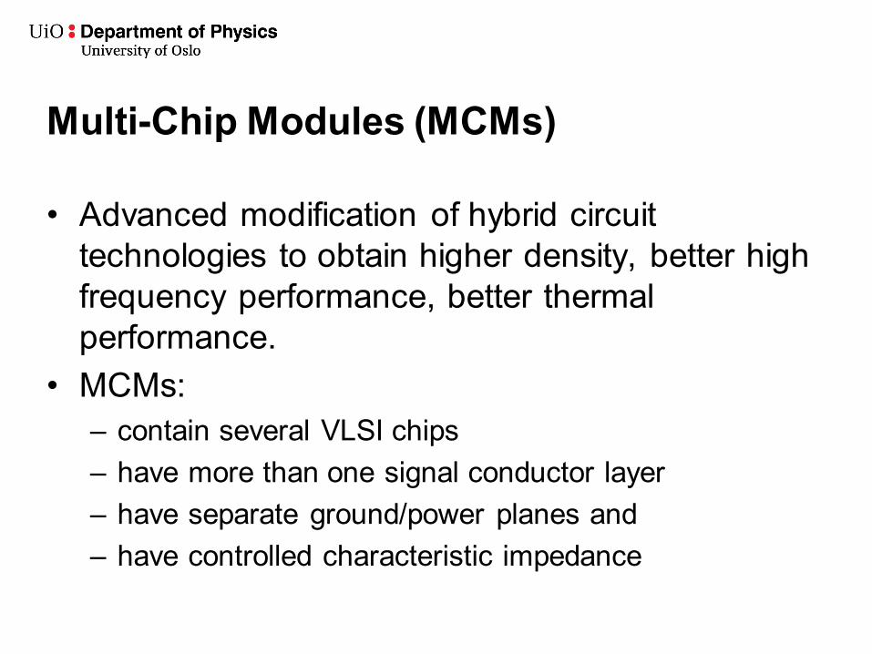
Multi-Chip Modules (MCMs)
• Advanced modification of hybrid circuit technologies to obtain higher density, better high frequency performance, better thermal performance.
• MCMs: – contain several VLSI chips – have more than one signal conductor layer – have separate ground/power planes and – have controlled characteristic impedance
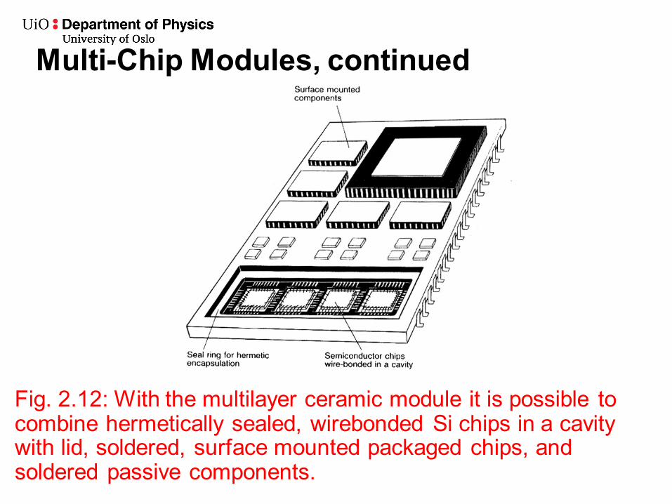
Multi-Chip Modules, continued
Fig. 2.12: With the multilayer ceramic module it is possible to combine hermetically sealed, wirebonded Si chips in a cavity with lid, soldered, surface mounted packaged chips, and soldered passive components.
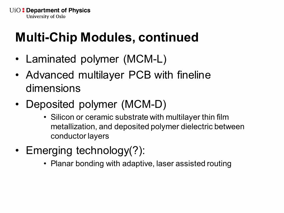
Multi-Chip Modules, continued • Laminated polymer (MCM-L) • Advanced multilayer PCB with fineline
dimensions • Deposited polymer (MCM-D)
• Silicon or ceramic substrate with multilayer thin film metallization, and deposited polymer dielectric between conductor layers
• Emerging technology(?): • Planar bonding with adaptive, laser assisted routing
Slide 44
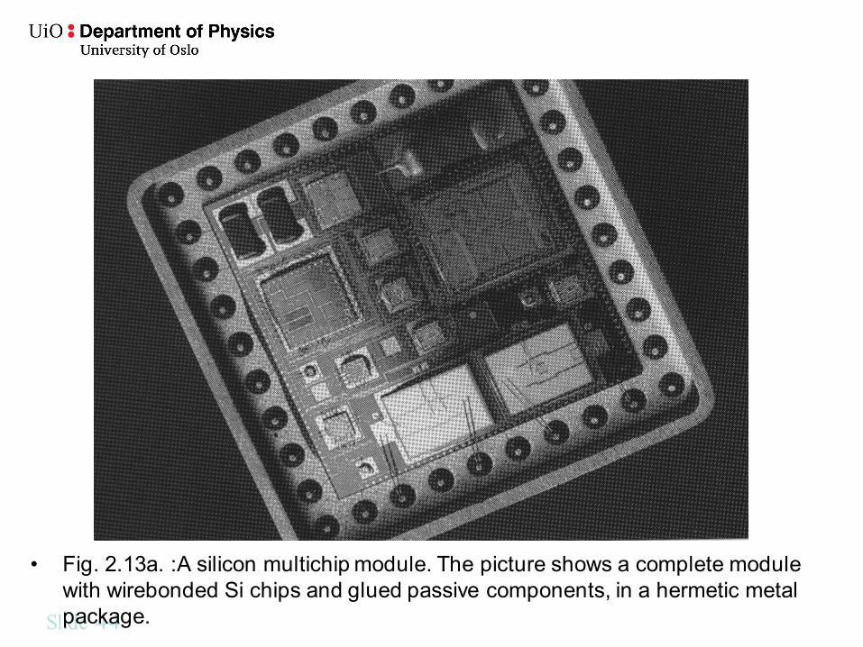
Multi-Chip Modules, continued
• Fig. 2.13a. :A silicon multichip module. The picture shows a complete module with wirebonded Si chips and glued passive components, in a hermetic metal package.
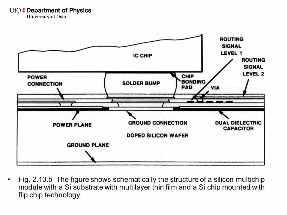
Multi-Chip Modules, continued
• Fig. 2.13.b The figure shows schematically the structure of a silicon multichip module with a Si substrate with multilayer thin film and a Si chip mounted with flip chip technology.
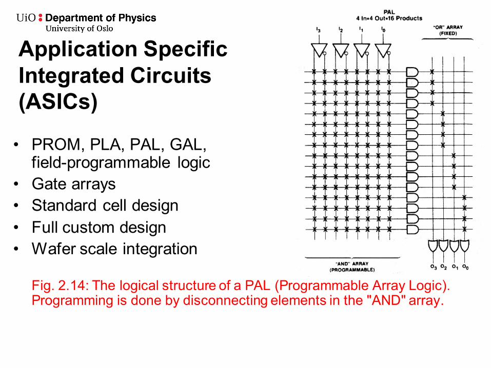
Application Specific Integrated Circuits (ASICs)
• PROM, PLA, PAL, GAL, field-programmable logic
• Gate arrays • Standard cell design • Full custom design • Wafer scale integration
Fig. 2.14: The logical structure of a PAL (Programmable Array Logic). Programming is done by disconnecting elements in the "AND" array.
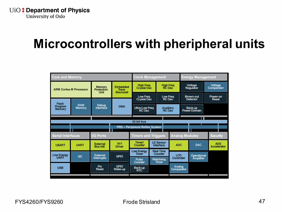
Microcontrollers with pheripheral units
FYS4260/FYS9260 Frode Strisland 47
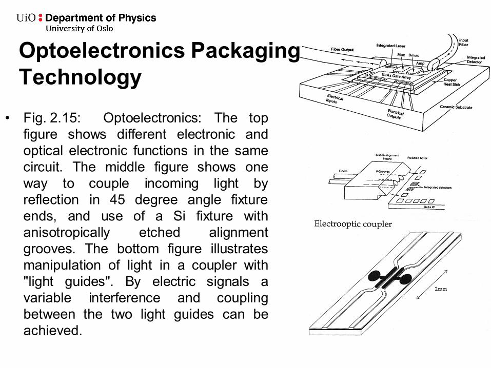
• Fig. 2.15: Optoelectronics: The top figure shows different electronic and optical electronic functions in the same circuit. The middle figure shows one way to couple incoming light by reflection in 45 degree angle fixture ends, and use of a Si fixture with anisotropically etched alignment grooves. The bottom figure illustrates manipulation of light in a coupler with "light guides". By electric signals a variable interference and coupling between the two light guides can be achieved.
Optoelectronics Packaging Technology
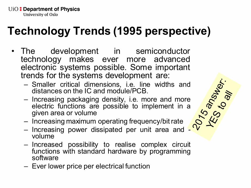
Technology Trends (1995 perspective) • The development in semiconductor
technology makes ever more advanced electronic systems possible. Some important trends for the systems development are: – Smaller critical dimensions, i.e. line widths and
distances on the IC and module/PCB. – Increasing packaging density, i.e. more and more
electric functions are possible to implement in a given area or volume
– Increasing maximum operating frequency/bit rate – Increasing power dissipated per unit area and -
volume – Increased possibility to realise complex circuit
functions with standard hardware by programming software
– Ever lower price per electrical function
Technology Trends, continued
• The established technology cannot satisfy the needs and requirements, and new technology always appears. It seems as if we hit physical limits on many fronts.
• However, earlier, when such limits have appeared, new ideas and new principles have been found.
• This will probably also happen in the future and will make the field of microelectronics dynamic and exciting in the future, for scientists as well as for users.
Unforeseen development 1995-2015 • Electronics go green:Lead soldering banned
– RoHS (The Restriction of Hazardous Substances Directive 2002/95/EC, (RoHS 1), short for Directive on the restriction of the use of certain hazardous substances in electrical and electronic equipment, was adopted in February 2003 by the European Union)
– Waste Electrical and Electronic Equipment Directive (WEEE) 2002/96/EC sets collection, recycling and recovery targets for electrical goods
• Consumer electronics revolution – Battery driven devices – mobile phones and pads – Wireless communication
• RF ID and Internet of Things • Nanoelectronics • Production of electronics moves abroad and to the far East • Rapid prototyping technology
FYS4260/FYS9260 Frode Strisland 51
Electronic Pack….. Chapter 2 Slide 52
Selecting the Optimal Technology
• The technology assessment should be done based upon detailed system specifications and other requirements for the product:
• Electrical specifications • Reliability and lifetime • Operating and environment conditions for the product.
Temperature, vibrations, electromagnetic radiation, etc. • Production volume • Available area/volume • Maintenance and reparability considerations • Acceptable price/cost level • Time-to-market • Etc.
Future Trends for Users and Designers of Electronic Systems
• The assortment of standard components is ever increasing, with availability of more and more complex integrated circuits and modules as standard components, with improved performance. Programmable standard components can be customised to specific applications.
• Emerging of industrial standards for specifications and documentation of standard technologies for easier communication between users, designers, producers, and subcontractors, with effective communication network based upon information technology. This infrastructure simplifies both bidding procedure and production by subcontractors, with decreasing importance of geographical closeness.
• Advanced technologies are emerging offering a broader range of features from high-end specifications to low cost than available in traditional technologies.
Future trends, continued
• Such advanced niche technologies are more specialised, making it inconvenient for most companies to have it as an in-house capability. This opens up a market with specialised subcontractor services.
• New product development should take technology assessment as an important task to be dealt with in detail with system optimisation in focus, all the way the initiation of the development.
• The market lifetime of the product is getting shorter and shorter, and therefore time-to-market must be minimised to obtain sufficient market penetration.
• These factors have had a large impact of the industry structure of the electronics business the last years - a restructuring that will probably continue for at least the next 5 - 10 years.
End of Chapter 2: Technologies for Electronics – Overview • Important issues:
– This is an overview chapter – we will later go in more details in the next chapters
– The most important Electronic Packaging & Interconnection Technologies described shortly here
• Please comment and discuss!