Embed Size (px)
Citation preview
3
GaAs Thermally Based MEMSDevices—Fabrication Techniques,Characterization and ModelingMEMS Device Design and Fabrication
MEMS Device Thermo-MechanicalCharacterization
MEMS Device Thermo-MechanicalModeling
Tibor Lalinsky1, Milan Drzık2, Jirı Jakovenko3, and Miroslav Husak3
1Institute of Electrical Engineering, Slovak Academy of Sciences, Dubravska cesta 9, 841 04Bratislava, Slovakia2International Laser Center, Ilkovicova 3, 812 19 Bratislava, Slovakia3Czech Technical University, Dept. of Microelectronics, Technicka 2, 166 27 Prague 6,Czech Republic
MEMS Device Design and Fabrication
1. INTRODUCTION
Silicon (Si) based MicroElectroMechanical Systems (MEMS) are now well understoodand widely used in various integrated micromachined microsensors and microactuators. Inrelation to this, gallium arsenide (GaAs) offers a number of material-related properties and
50 TIBOR LALINSKY ET AL.
technological advantages over Si [1–3]. These include well know properties, such as directband gap transition and high electron mobility.
A very important feature of GaAs is the possibility of forming compatible ternaryand quaternary compounds by alloying. Using GaAs as a substrate material, formation ofAlx Ga1−x As is especially attractive, since their lattice constants are nearly equal, and alu-minum and gallium atoms are easily substituted in the lattice without causing too muchstrain in the film. Thanks to this prominent feature, a number of interesting properties andphenomena, such as high-mobility two-dimensional carrier gases, resonant tunneling, andfractional quantum Hall effect, have been found in the Alx Ga1−x As/GaAs heterostructuresystem. New devices, such as modulation-doped FETs, heterojunction bipolar transistors,hot electron transistors, resonant tunneling transistors, quantum-well lasers, and other pho-tonic and quantum effect devices, have been developed using this heterostructure system.The heterostructure system seems to be of primary importance also for the investigation ofnew one- and zero-dimensional effects in structures, such as quantum wires and dots. Theseareas are recognized to be very interesting from the viewpoint of semiconductor physicsand device engineering.
GaAs also has piezoelectric properties comparable with those of quartz. The piezoelec-tric response of GaAs is an attractive feature. It gives the possibility of activating motionsby an electric field and of detecting motions by bound charges generated by the mechanicalstress [4]. Other advantages with piezoelectricity are negligible thermal gradients due to thelow activation power (of the order of μW), and the possibility of detecting very small me-chanical amplitudes. The response time of the piezoelectric effect is limited by Maxwell’sequations and, therefore, it is extremely small. In general, the response time is restrictedby mechanical damping of the structure. The piezoelectric effect in GaAs is well suited forresonant sensors and actuators.
GaAs also exhibits a very interesting piezoresistive response [2]. In GaAs, the physicalmechanisms that change the resistance due to an applied stress are different from those insilicon. One response mechanism is the observed mobility change due to the change of theelectron effective mass with pressure. Another mechanism is a pressure induced transfer ofelectrons from the high-mobility band gap minimum � to low mobility minimum X or L dueto a change of their relative energy. The third response mechanism is the pressure inducedfreezing of electrons to deep level impurity states DX, observed mainly for Alx Ga1−x Asepitaxial layers of compositions about x = 0.3 − 0.35. The fourth response mechanism issomewhat different from the others, using the stress gradient induced piezoelectric boundcharges to change the resistivity in a diffused resistor. Combination of piezoresistive andpiezoelectric effects in a GaAs two-dimensional electron gas (2DEG) layer yields a highereffective piezoresistive coefficient compared with Si [5]. The piezoresistive coefficient ofGaAs with 2DEG (�L = 46 × 10−10 m2/N) is almost 10 times higher than that of Si (�L =5.7 × 10⁻¹⁰ m2/N).
Further GaAs response mechanisms, such as thermoresistive, piezooptic and directband gap responses, may also be found in [2].
GaAs is also an attractive material for thermal sensors because it can operate at ambienttemperatures up to 350 ◦C thanks to its wide band gap. The higher thermal resistivity andhigher Seebeck coefficient, as compared with Si, make it a very promising material forsuch MEMS devices as microwave power sensors, gas sensors and flow sensors. Usingvarious micromachining techniques it is possible to fabricate free-standing micromechanical

GaAs THERMALLY BASED MEMS DEVICES 51
structures that are thermally isolated from the bulk material, allowing realization of thermalbased MEMS devices.
Likewise, the initial MBE and MOCVD grown GaAs heterostructures provide moreflexibility and precision in micromachining, which results in very sharp interfaces (one ortwo monolayers). Due to different compositions, these layers can easily be etched by wetor dry etching techniques with excellent compositional selectivity. Precise control of thethickness and uniformity of GaAs based micromechanical structures like cantilever beams[3, 6, 7], membranes or bridges [1, 8–11] can be achieved directly via the thickness of theMBE grown materials over an etch stop layer.
Additional advantages can also be taken by the well-controlled mechanical characteris-tics offered by single-crystalline epitaxial layers. The measured fracture properties of GaAsare known to be sufficiently good with average fracture strength of 2.7 GPa (i.e., at leastthree times as high as that of most construction steels) [1, 2].
Technological advantages and intrinsic physical properties of GaAs heterostructureshave been demonstrated in various MEMS based on GaAs solid state device and microme-chanical structure technology [1, 3, 9–18]. Most of them were designed for applicationas micromachined microsensors for electrical power sensing [3, 12–16], infrared thermalradiation detection [18] and for pressure sensing [10, 11].
In order to demonstrate the high resistivity and micromachining capabilities of GaAs,micromachined coplanar waveguides have been developed [17, 19] to suppress high-frequency losses at millimeter and submillimeter wavelengths. Moreover, a suspendedplanar spiral inductor and a micromachined GaAs/metal thermopile [1], and a suspendedGaAs resistor [9] as special micromechanical devices have also been demonstrated for GaAsMEMS design. The introduction of new material families, such as AlGaAs/GaAs, offeredcompatibility of the micromechanical devices with the MESFET or pHEMT technology,so that they can be integrated with GaAs based monolithic microwave integrated circuits(MMICs).
A GaAs cantilever has also been introduced as a micromechanical device for fabrica-tion of novel probes for scanning probe microscopy (SPM). Recently, the developments inthe field of micromachined technology of GaAs cantilevers with integrated tips like thoseof atomic force microscopy (AFM) cantilevers have been successfully reported [20, 21].These cantilevers represent the basic sensor design for both passive as well as active scan-ning near field probes. For example, using an integrated Schottky diode as a temperaturesensor and photodetector in a GaAs tip, great potentials for the development of scanningthermal microscopy (SThM) and scanning near-field optical microscopy (SNOM) can bepredicted. Likewise, the combination of standard III–V based epitaxy techniques (MBE orMOCVD) with 3D growth of different layer heterostructures for light-emitting and laserdiodes or quantum dots on the tip is a challenge for future new concepts of GaAs basedMicro(Nano)OptoElectroMechanical System-M(N)OEMS devices.
In addition, the bimetallic effect was observed in 2 μm thick GaAs cantilever beams of apower sensor microsystem [14, 22, 23]. Cantilever deflections were induced by differentialthermal expansion of the cantilever layers using GaAs MESFET as a heater.
Thermal actuation of suspended GaAs membrane Bragg reflectors has been performedto tune the Fabry-Perot filters [24]. Four supporting membrane bridges have been usedwith resistor heaters as driving elements. Thermal actuation of the membrane yielded amechanical sensitivity of 13 nm/mW under normal pressure.

52 TIBOR LALINSKY ET AL.
TABLE 1. Structural, thermal and mechanical properties of Si, GaAs and AlAs [2]
Semiconductor materials Si GaAs AIAs
Crystal structure Diamond Zincblende Zincblende
Lattice constant, a (A) 5.4311 5.6533 5.6611
Density, ρ (103 kg m−3) 2.3290 5.360 3.760
Melting point, TM(◦C) 1413 1238 1740
Specific heat, Cp(J g−1 K−1) 0.71 0.35 0.48
Thermal resistivity, W (K cm W−1) 0.64 2.27 1.1
Thermal expansion coefficient, α11(10−6 ◦C−1) 2.6 6.4 5.2
Debay temperature, θD(K) 463 370 446
Fracture toughness, K (MPa m1/2) 0.9 0.44 1.7
Hardness, Hv(100) (GPa) 10 7 5
Stiffness constants (GPa)
c11 165.6 118.8 120.2
c12 63.98 53.8 57.0
c44 79.51 58.9 58.9
Elastic compliance constants (10−12 Pa−1)
s11 7.7 11.7 12
s12 −2.1 −3.1 −3.9
s44 12.6 16.8 17
Piezoelectric coefficient d14 (pm/V) 0 −2.69 −3.82
A comprehensive electro-mechanical performance analysis of a thermally actuatedGaAs cantilever was also reported [25, 26]. An integrated GaAs MESFET heater was used toactuate a 2 μm thick GaAs cantilever. Simultaneously, a Schottky gate diode of a MESFETwas used to sense the cantilever temperature corresponding to various levels of powerdissipation. The analyzed device has shown an excellent linearity in the electro-thermo-mechanical conversion characteristics and high electro-mechanical conversion efficiency(�E = 802 nm/mW). The dynamic behavior of the GaAs cantilever was tested with a squarewave signal. The mechanical time constant of 1.4 ms obtained from the measured timeresponse of the cantilever deflection was found to be limited by the electro-thermal timeresponse. The resonant frequency of the cantilever as high as 15.44 kHz was measured.
Based on this short review devoted to design and fabrication of various micromachinedGaAs based devices and structures it should be noted that both GaAs and AlGaAs materialsseem to be the basic electronical and construction materials for MEMS design, mainlythanks to their structural, electrical and thermo-mechanical properties. The basic structural,electrical, mechanical and thermal properties of both materials have been well-introducedby many of authors. They can be found, for example, in [2, 27–32]. For comparison, someof their properties are also summarized in Table 1 [2].
In this chapter, various GaAs micromachining approaches compatible with GaAs het-erostructure based device fabrication techniques are introduced. Special attention is givento GaAs thermally based MEMS devices because they directly demonstrate the necessityfor mutually compatible integration of the micromechanical structures with the MESFETor HEMT high-speed devices. Efforts are made to cover the basic fabrication technolo-gies, techniques, processes, and materials. One of the main goals is to show how to in-tegrate GaAs microelectronic devices with GaAs micromechanical structures in order toproduce integrated high performance MEMS. This chapter introduces the mentioned groupof MEMS devices in all their complexity and multidisciplinary basis. Therefore, besides
GaAs THERMALLY BASED MEMS DEVICES 53
fabrication methods, non-conventional optical methods are introduced to analyze the ba-sic thermo-mechanical properties of the MEMS devices. They permit (in situ) to studythree-dimensional (3D) device nano-deformations induced by temperature changes in bothstationary and non-stationary dynamic process conditions. Finally, various approaches anddesign concepts in the field of 3D thermo-mechanical modeling and simulation are also intro-duced and directly compared with comprehensive experimental electro-thermo-mechanicalcharacterization of the MEMS devices. In general, these model approaches demonstratea great potential for studying the thermo-mechanical phenomena and effects observed inMEMS devices on the required micro- and nanoscale. They are considered to be indispens-able for the design of novel 3D GaAs thermally based MEMS devices.
2. DESCRIPTION OF GaAs THERMALLY BASED MEMS
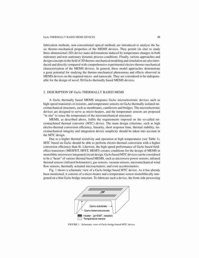
A GaAs thermally based MEMS integrates GaAs microelectronic devices such ashigh-speed transistors or resistors, and temperature sensors on GaAs thermally isolated mi-cromechanical structures, such as membranes, cantilevers and bridges. The microelectronicdevices are designed to serve as micro-heaters, and the temperature sensors are proposed“in situ” to sense the temperature of the micromechanical structures.
MEMS, as described above, fulfils the requirements imposed on the so-called mi-cromachined thermal converter (MTC) device. The main design criterions, such as highelectro-thermal conversion efficiency, linearity, short response time, thermal stability, mi-cromechanical integrity and integration device simplicity should be taken into account inthe MTC design.
Due to a higher thermal resistivity and operation at high temperatures (see Table 1),MTC based on GaAs should be able to perform electro-thermal conversion with a higherconversion efficiency than Si. Likewise, the high-speed performance of GaAs based field-effect transistors (MESFET, HFET, HEMT) creates conditions for the design of MEMS inmonolithic microwave integrated circuit design. GaAs based MTC devices can be consideredto be a “heart” of various thermal based MEMS, such as microwave power sensors, infraredthermal sensors (infrared bolometers), gas sensors, vacuum sensors, micromechanical windflow sensors, thermally actuated microactuators, and even accelerometers.
Fig. 1 shows a schematic view of a GaAs bridge based MTC device. As it has alreadybeen mentioned, it consists of a micro-heater and a temperature sensor monolithically inte-grated on a thin GaAs bridge structure. To fabricate such a device, the front-side processing
FIGURE 1. Schematic view of GaAs bridge based MTC device.
54 TIBOR LALINSKY ET AL.
technology of the micro-heater and temperature sensor must be combined with surfaceand bulk micromachining of GaAs. As a rule, GaAs micromachining technology shouldbe fully compatible with the processing technology of integrated microelectronic devices.Therefore, in the next parts of this chapter the basic GaAs micromachining techniques andMEMS fabrication technologies are described in detail.
3. GaAs MICROMACHINING TECHNIQUES
In GaAs micromachining, wet and dry etching processes are widely used. Wet etchantsare categorized as isotropic etchants (attack the material being etched at the same rate inall directions) and anisotropic etchants (attack the material or GaAs at different rates indifferent directions, and therefore, shapes/geometry can be precisely controlled). In otherwords, the isotropic etching has a uniform etch rate at all orientations, while for anisotropicetching, the etch rate depends on crystal orientation.
The dry etching process often used in GaAs micromachining is reactive ion etching(RIE). In this process, ions are accelerated towards the material to be etched, and the etchingreaction is enhanced in the direction of ion trajectory. Reactive ion etching is therefore ananisotropic etching process.
Selectivity of the etching process is the most important property utilized in GaAsmicromachining. It is defined as a ratio between the structural material (slower etching)and sacrificial material (faster etching) etch rates for a specific etchant. For a few sys-tems, entirely selective etching can be achieved allowing real etch stop materials. Themost frequently used sacrificial wet and dry etch systems for III–V compound heterostruc-tures are presented in [33, 34]. It can be noted that not only different materials but alsodifferent dopant concentrations and damaged regions could act as stop and sacrificiallayers.
A great number of micromachining techniques have already been developed for GaAs,such as selective etch stops for hetero- and homostructures of various electrical properties,sacrificial layer techniques with various etch rate selectivities, and dry and wet etching forisotropic and anisotropic shaping.
Two main methods can be applied to fabricate GaAs micromechanical structures: bulkmicromachining, where structures are etched in the substrate, and surface micromachining,where micromechanical layers are formed from layers deposited onto the surface. In bulkmicromachining, two different approaches have been considered: etching from the frontside and from the back side of the wafer.
Front Side Bulk Micromachining
In the case of front side bulk micromachining, sacrificial damaged GaAs layers createdby high energy ion implantation of nitrogen can be used [35, 36]. Energy ions effectivelyproduce a lot of damage in GaAs. The displaced atoms in the damaged regions are chemicallyless stable than the original GaAs atoms. If a layer has a sufficient density of displaced atoms,it can be used as a sacrificial layer, selectively removable by defect-sensitive etchants. Deeplow-dose nitrogen implantation can also compensate n-doped GaAs to n-GaAs at the top,which then can be used as an etch stop layer if electrolytic etching techniques are applied. On
GaAs THERMALLY BASED MEMS DEVICES 55
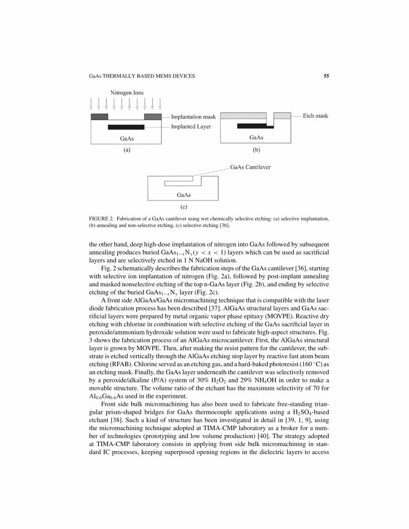
FIGURE 2. Fabrication of a GaAs cantilever using wet chemically selective etching: (a) selective implantation,
(b) annealing and non-selective etching, (c) selective etching [36].
the other hand, deep high-dose implantation of nitrogen into GaAs followed by subsequentannealing produces buried GaAs1−x Ny(y < x < 1) layers which can be used as sacrificiallayers and are selectively etched in 1 N NaOH solution.
Fig. 2 schematically describes the fabrication steps of the GaAs cantilever [36], startingwith selective ion implantation of nitrogen (Fig. 2a), followed by post-implant annealingand masked nonselective etching of the top n-GaAs layer (Fig. 2b), and ending by selectiveetching of the buried GaAs1−x Ny layer (Fig. 2c).
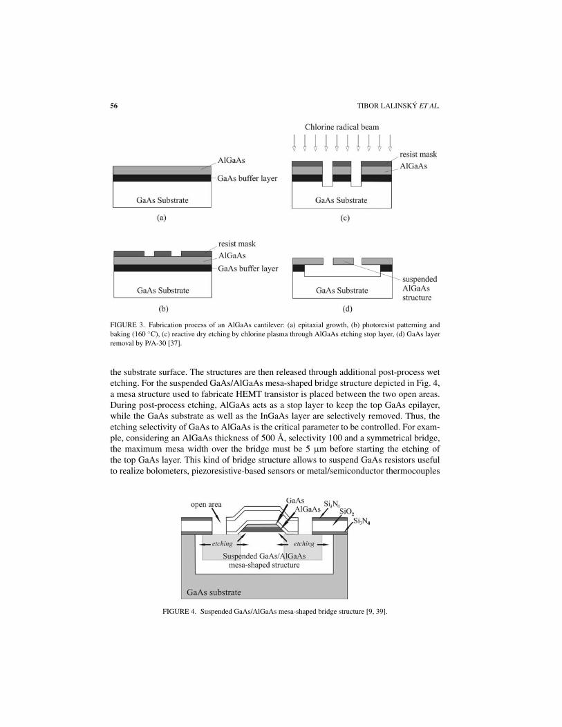
A front side AlGaAs/GaAs micromachining technique that is compatible with the laserdiode fabrication process has been described [37]. AlGaAs structural layers and GaAs sac-rificial layers were prepared by metal organic vapor phase epitaxy (MOVPE). Reactive dryetching with chlorine in combination with selective etching of the GaAs sacrificial layer inperoxide/ammonium hydroxide solution were used to fabricate high-aspect structures. Fig.3 shows the fabrication process of an AlGaAs microcantilever. First, the AlGaAs structurallayer is grown by MOVPE. Then, after making the resist pattern for the cantilever, the sub-strate is etched vertically through the AlGaAs etching stop layer by reactive fast atom beametching (RFAB). Chlorine served as an etching gas, and a hard-baked photoresist (160 ◦C) asan etching mask. Finally, the GaAs layer underneath the cantilever was selectively removedby a peroxide/alkaline (P/A) system of 30% H2O2 and 29% NH4OH in order to make amovable structure. The volume ratio of the etchant has the maximum selectivity of 70 forAl0.6Ga0.4As used in the experiment.
Front side bulk micromachining has also been used to fabricate free-standing trian-gular prism-shaped bridges for GaAs thermocouple applications using a H2SO4-basedetchant [38]. Such a kind of structure has been investigated in detail in [39, 1, 9], usingthe micromachining technique adopted at TIMA-CMP laboratory as a broker for a num-ber of technologies (prototyping and low volume production) [40]. The strategy adoptedat TIMA-CMP laboratory consists in applying front side bulk micromachining in stan-dard IC processes, keeping superposed opening regions in the dielectric layers to access
56 TIBOR LALINSKY ET AL.
FIGURE 3. Fabrication process of an AlGaAs cantilever: (a) epitaxial growth, (b) photoresist patterning and
baking (160 ◦C), (c) reactive dry etching by chlorine plasma through AlGaAs etching stop layer, (d) GaAs layer
removal by P/A-30 [37].
the substrate surface. The structures are then released through additional post-process wetetching. For the suspended GaAs/AlGaAs mesa-shaped bridge structure depicted in Fig. 4,a mesa structure used to fabricate HEMT transistor is placed between the two open areas.During post-process etching, AlGaAs acts as a stop layer to keep the top GaAs epilayer,while the GaAs substrate as well as the InGaAs layer are selectively removed. Thus, theetching selectivity of GaAs to AlGaAs is the critical parameter to be controlled. For exam-ple, considering an AlGaAs thickness of 500 A, selectivity 100 and a symmetrical bridge,the maximum mesa width over the bridge must be 5 μm before starting the etching ofthe top GaAs layer. This kind of bridge structure allows to suspend GaAs resistors usefulto realize bolometers, piezoresistive-based sensors or metal/semiconductor thermocouples
FIGURE 4. Suspended GaAs/AlGaAs mesa-shaped bridge structure [9, 39].

GaAs THERMALLY BASED MEMS DEVICES 57
FIGURE 5. Free standing triangular prism-shaped bridge structure [9, 39].
for infrared thermopile sensors. The triangular prism-shaped bridge structure illustrated inFig. 5 can be obtained via selective anisotropic etching. Experimental details of the etchingprocess can be found in [9, 39]. This type of bridge structure is suitable for fabricationof free-standing active devices (diodes and transistors) or thermal sensors, as mentionedlater on.
Back Side Bulk Micromachining
The back side bulk micromachining commonly involves stopping on an epitaxial layer.Additional masking on the back side and special alignment techniques are required. Becauseof the high selectivity of the GaAs/AlGaAs system, it is possible to etch several hundredmicrometers of GaAs, stopping at an exact depth defined by a stop layer of AlGaAs. Thistechnique has been widely used to fabricate GaAs membranes [10, 11, 15, 16], cantilevers[3, 6, 7, 12–14] and bridges [19].
Fig. 6 shows a cross-section through a GaAs membrane patterned by the back sidewet chemical etching technique [10]. Definition of the membrane was done by using fastetching over 400 μm. An unselective etchant H2SO4:H2O2:H2O with concentration ratio4:3:3 was used in the bubble etch method. Then etching continues with selective etchantNH4OH:H2O2 with concentration ratio 1:24. Etching continues until the AlAs etch stoplayers are reached. This isotropic etchant has a selectivity of 1000 and pH around 8. TheAlAs etch stop is removed using diluted HF which has a selectivity of 107. A simplifieddescription of such a process is also depicted in Fig. 7 [11]. The back side etch mask is

58 TIBOR LALINSKY ET AL.
FIGURE 6. A cross-section through GaAs membrane patterned by back side wet chemical etching technique [10].
patterned in the first step. Then, fast unselective etching is performed, followed by slowerselective etching, stopping at the AlGaAs layer.
Besides the mentioned wet etching techniques, anisotropic dry etching techniques havealso been developed for back side bulk GaAs micromachining [3, 6, 7, 12]. The etchingexperiments were aimed at establishing the etch conditions which would best meet thefollowing process requirements:
• sufficient etch rate of GaAs for deep back side RIE through a GaAs substrate to theetch stop layer, with anisotropy needed to minimize lateral undercutting,
• selectivity of GaAs etching to the etch masks to achieve back side over-etching ofthe GaAs substrate to the stop layer,
• selectivity of GaAs to AlGaAs etching needed for smooth bottom of the back sideetched cantilevers.
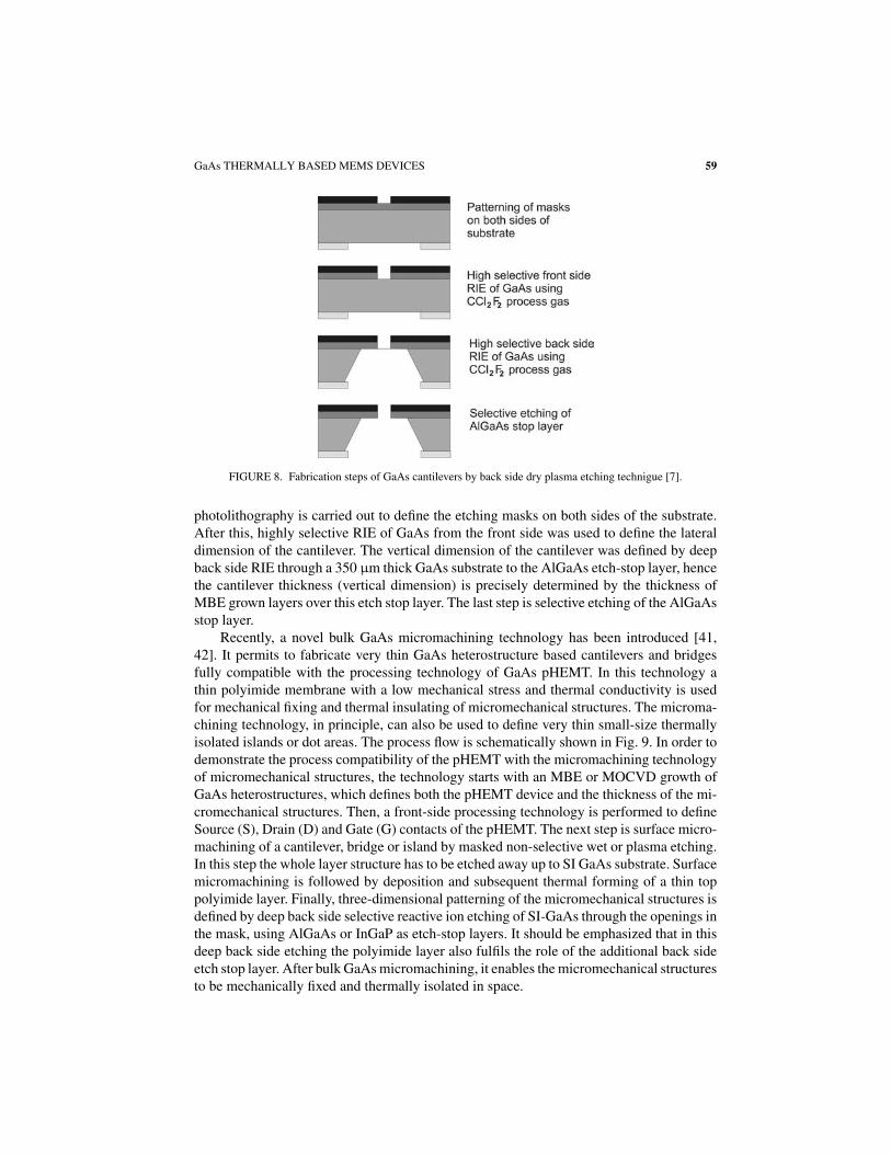
CCl2F2 was used as the process gas, the chamber pressure during etching being 10, 20and 30 Pa at a gas flow of 30 sccm. The RF power was varied from 50 to 150 W. Fig. 8shows the basic fabrication steps of 2 μm thick GaAs cantilevers [7]. The GaAs/AlGaAs het-erostructure layer system grown by MBE was designed to be used for both GaAs MESFETtechnology and micromechanical structures fabrication. In the first step, double-side aligned
FIGURE 7. Back side GaAs bulk micromachining using AlGaAs as etch stop layer [11].
GaAs THERMALLY BASED MEMS DEVICES 59
FIGURE 8. Fabrication steps of GaAs cantilevers by back side dry plasma etching technigue [7].
photolithography is carried out to define the etching masks on both sides of the substrate.After this, highly selective RIE of GaAs from the front side was used to define the lateraldimension of the cantilever. The vertical dimension of the cantilever was defined by deepback side RIE through a 350 μm thick GaAs substrate to the AlGaAs etch-stop layer, hencethe cantilever thickness (vertical dimension) is precisely determined by the thickness ofMBE grown layers over this etch stop layer. The last step is selective etching of the AlGaAsstop layer.
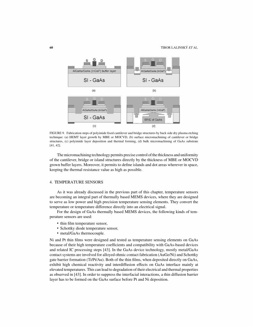
Recently, a novel bulk GaAs micromachining technology has been introduced [41,42]. It permits to fabricate very thin GaAs heterostructure based cantilevers and bridgesfully compatible with the processing technology of GaAs pHEMT. In this technology athin polyimide membrane with a low mechanical stress and thermal conductivity is usedfor mechanical fixing and thermal insulating of micromechanical structures. The microma-chining technology, in principle, can also be used to define very thin small-size thermallyisolated islands or dot areas. The process flow is schematically shown in Fig. 9. In order todemonstrate the process compatibility of the pHEMT with the micromachining technologyof micromechanical structures, the technology starts with an MBE or MOCVD growth ofGaAs heterostructures, which defines both the pHEMT device and the thickness of the mi-cromechanical structures. Then, a front-side processing technology is performed to defineSource (S), Drain (D) and Gate (G) contacts of the pHEMT. The next step is surface micro-machining of a cantilever, bridge or island by masked non-selective wet or plasma etching.In this step the whole layer structure has to be etched away up to SI GaAs substrate. Surfacemicromachining is followed by deposition and subsequent thermal forming of a thin toppolyimide layer. Finally, three-dimensional patterning of the micromechanical structures isdefined by deep back side selective reactive ion etching of SI-GaAs through the openings inthe mask, using AlGaAs or InGaP as etch-stop layers. It should be emphasized that in thisdeep back side etching the polyimide layer also fulfils the role of the additional back sideetch stop layer. After bulk GaAs micromachining, it enables the micromechanical structuresto be mechanically fixed and thermally isolated in space.
60 TIBOR LALINSKY ET AL.
FIGURE 9. Fabrication steps of polyimide fixed cantilever and bridge structures by back side dry plasma etching
technique: (a) HEMT layer growth by MBE or MOCVD, (b) surface micromachining of cantilever or bridge
structures, (c) polyimide layer deposition and thermal forming, (d) bulk micromachining of GaAs substrate
[41, 42].
The micromachining technology permits precise control of the thickness and uniformityof the cantilever, bridge or island structures directly by the thickness of MBE or MOCVDgrown buffer layers. Moreover, it permits to define islands and dot areas wherever in space,keeping the thermal resistance value as high as possible.
4. TEMPERATURE SENSORS
As it was already discussed in the previous part of this chapter, temperature sensorsare becoming an integral part of thermally based MEMS devices, where they are designedto serve as low power and high precision temperature sensing elements. They convert thetemperature or temperature difference directly into an electrical signal.
For the design of GaAs thermally based MEMS devices, the following kinds of tem-perature sensors are used:
• thin film temperature sensor,• Schottky diode temperature sensor,• metal/GaAs thermocouple.
Ni and Pt thin films were designed and tested as temperature sensing elements on GaAsbecause of their high temperature coefficients and compatibility with GaAs-based devicesand related IC processing steps [43]. In the GaAs device technology, mostly metal/GaAscontact systems are involved for alloyed ohmic contact fabrication (AuGe/Ni) and Schottkygate barrier formation (Ti/Pt/Au). Both of the thin films, when deposited directly on GaAs,exhibit high chemical reactivity and interdiffusion effects on GaAs interface mainly atelevated temperatures. This can lead to degradation of their electrical and thermal propertiesas observed in [43]. In order to suppress the interfacial interactions, a thin diffusion barrierlayer has to be formed on the GaAs surface before Pt and Ni deposition.
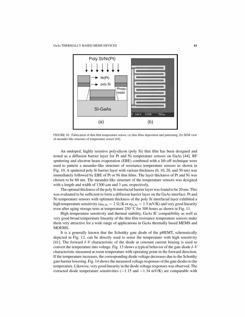
GaAs THERMALLY BASED MEMS DEVICES 61
FIGURE 10. Fabrication of thin film temperature sensor, (a) thin films deposition and patterning, (b) SEM view
of meander-like structure of temperature sensor [44].
An undoped, highly resistive polysilicon (poly Si) thin film has been designed andtested as a diffusion barrier layer for Pt and Ni temperature sensors on GaAs [44]. RFsputtering and electron beam evaporation (EBE) combined with a lift-off technique wereused to pattern a meander-like structure of resistance temperature sensors as shown inFig. 10. A sputtered poly Si barrier layer with various thickness (0, 10, 20, and 30 nm) wasimmediately followed by EBE of Pt or Ni thin films. The layer thickness of Pt and Ni waschosen to be 60 nm. The meander-like structure of the temperature sensors was designedwith a length and width of 1300 μm and 3 μm, respectively.
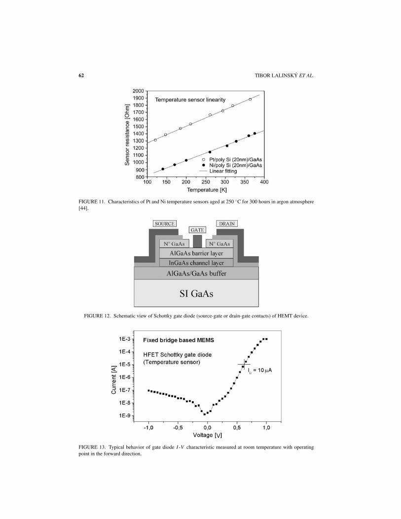
The optimal thickness of the poly Si interfacial barrier layer was found to be 20 nm. Thiswas evaluated to be sufficient to form a diffusion barrier layer on the GaAs interface. Pt andNi temperature sensors with optimum thickness of the poly Si interfacial layer exhibited ahigh temperature sensitivity (αPt,Ni > 2 �/K or αPt,Ni > 1.5 mV/K) and very good linearityeven after aging storage tests at temperature 250 ◦C for 300 hours as shown in Fig. 11.
High temperature sensitivity and thermal stability, GaAs IC compatibility as well asvery good broad temperature linearity of the thin film resistance temperature sensors makethem very attractive for a wide range of applications in GaAs thermally based MEMS andMOEMS.
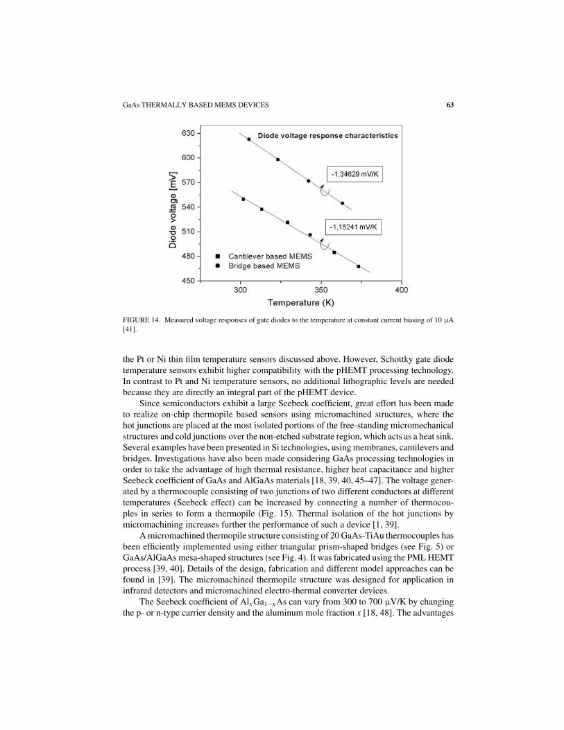
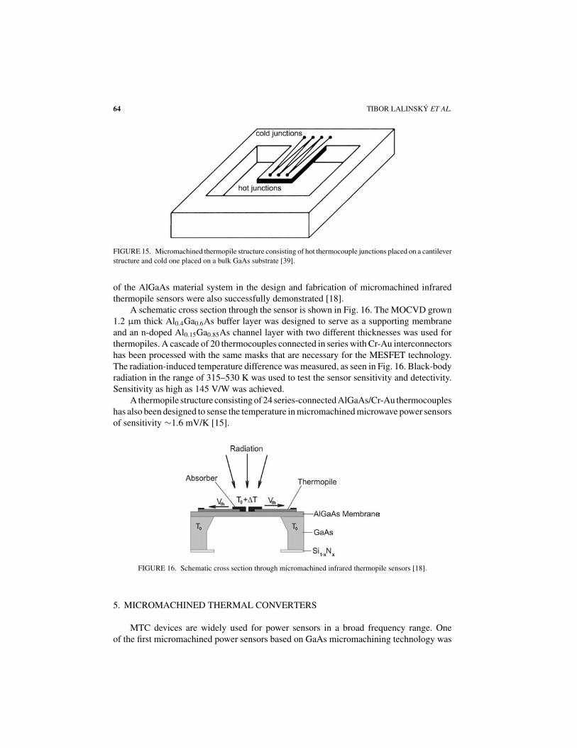
It is a generally known that the Schottky gate diode of the pHEMT, schematicallydepicted in Fig. 12, can be directly used to sense the temperature with high sensitivity[41]. The forward I–V characteristic of the diode at constant current biasing is used toconvert the temperature into voltage. Fig. 13 shows a typical behavior of the gate diode I–Vcharacteristic measured at room temperature with operating point in the forward direction.If the temperature increases, the corresponding diode voltage decreases due to the Schottkygate barrier lowering. Fig. 14 shows the measured voltage responses of the gate diodes to thetemperature. Likewise, very good linearity in the diode voltage responses was observed. Theextracted diode temperature sensitivities (−1.15 and −1.34 mV/K) are comparable with
62 TIBOR LALINSKY ET AL.
FIGURE 11. Characteristics of Pt and Ni temperature sensors aged at 250 ◦C for 300 hours in argon atmosphere
[44].
FIGURE 12. Schematic view of Schottky gate diode (source-gate or drain-gate contacts) of HEMT device.
FIGURE 13. Typical behavior of gate diode I -V characteristic measured at room temperature with operating
point in the forward direction.
GaAs THERMALLY BASED MEMS DEVICES 63
FIGURE 14. Measured voltage responses of gate diodes to the temperature at constant current biasing of 10 μA
[41].
the Pt or Ni thin film temperature sensors discussed above. However, Schottky gate diodetemperature sensors exhibit higher compatibility with the pHEMT processing technology.In contrast to Pt and Ni temperature sensors, no additional lithographic levels are neededbecause they are directly an integral part of the pHEMT device.
Since semiconductors exhibit a large Seebeck coefficient, great effort has been madeto realize on-chip thermopile based sensors using micromachined structures, where thehot junctions are placed at the most isolated portions of the free-standing micromechanicalstructures and cold junctions over the non-etched substrate region, which acts as a heat sink.Several examples have been presented in Si technologies, using membranes, cantilevers andbridges. Investigations have also been made considering GaAs processing technologies inorder to take the advantage of high thermal resistance, higher heat capacitance and higherSeebeck coefficient of GaAs and AlGaAs materials [18, 39, 40, 45–47]. The voltage gener-ated by a thermocouple consisting of two junctions of two different conductors at differenttemperatures (Seebeck effect) can be increased by connecting a number of thermocou-ples in series to form a thermopile (Fig. 15). Thermal isolation of the hot junctions bymicromachining increases further the performance of such a device [1, 39].
A micromachined thermopile structure consisting of 20 GaAs-TiAu thermocouples hasbeen efficiently implemented using either triangular prism-shaped bridges (see Fig. 5) orGaAs/AlGaAs mesa-shaped structures (see Fig. 4). It was fabricated using the PML HEMTprocess [39, 40]. Details of the design, fabrication and different model approaches can befound in [39]. The micromachined thermopile structure was designed for application ininfrared detectors and micromachined electro-thermal converter devices.
The Seebeck coefficient of Alx Ga1−x As can vary from 300 to 700 μV/K by changingthe p- or n-type carrier density and the aluminum mole fraction x [18, 48]. The advantages
64 TIBOR LALINSKY ET AL.
FIGURE 15. Micromachined thermopile structure consisting of hot thermocouple junctions placed on a cantilever
structure and cold one placed on a bulk GaAs substrate [39].
of the AlGaAs material system in the design and fabrication of micromachined infraredthermopile sensors were also successfully demonstrated [18].
A schematic cross section through the sensor is shown in Fig. 16. The MOCVD grown1.2 μm thick Al0.4Ga0.6As buffer layer was designed to serve as a supporting membraneand an n-doped Al0.15Ga0.85As channel layer with two different thicknesses was used forthermopiles. A cascade of 20 thermocouples connected in series with Cr-Au interconnectorshas been processed with the same masks that are necessary for the MESFET technology.The radiation-induced temperature difference was measured, as seen in Fig. 16. Black-bodyradiation in the range of 315–530 K was used to test the sensor sensitivity and detectivity.Sensitivity as high as 145 V/W was achieved.
A thermopile structure consisting of 24 series-connected AlGaAs/Cr-Au thermocoupleshas also been designed to sense the temperature in micromachined microwave power sensorsof sensitivity ∼1.6 mV/K [15].
FIGURE 16. Schematic cross section through micromachined infrared thermopile sensors [18].
5. MICROMACHINED THERMAL CONVERTERS
MTC devices are widely used for power sensors in a broad frequency range. Oneof the first micromachined power sensors based on GaAs micromachining technology was
GaAs THERMALLY BASED MEMS DEVICES 65
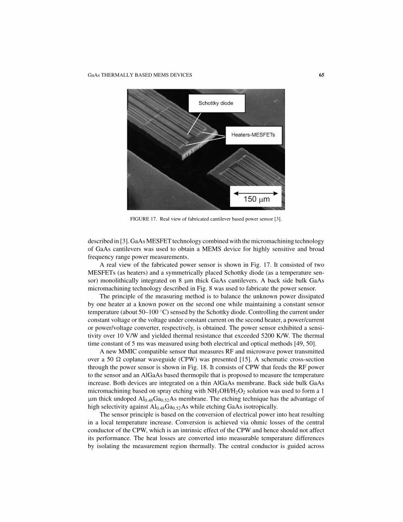
FIGURE 17. Real view of fabricated cantilever based power sensor [3].
described in [3]. GaAs MESFET technology combined with the micromachining technologyof GaAs cantilevers was used to obtain a MEMS device for highly sensitive and broadfrequency range power measurements.
A real view of the fabricated power sensor is shown in Fig. 17. It consisted of twoMESFETs (as heaters) and a symmetrically placed Schottky diode (as a temperature sen-sor) monolithically integrated on 8 μm thick GaAs cantilevers. A back side bulk GaAsmicromachining technology described in Fig. 8 was used to fabricate the power sensor.
The principle of the measuring method is to balance the unknown power dissipatedby one heater at a known power on the second one while maintaining a constant sensortemperature (about 50–100 ◦C) sensed by the Schottky diode. Controlling the current underconstant voltage or the voltage under constant current on the second heater, a power/currentor power/voltage converter, respectively, is obtained. The power sensor exhibited a sensi-tivity over 10 V/W and yielded thermal resistance that exceeded 5200 K/W. The thermaltime constant of 5 ms was measured using both electrical and optical methods [49, 50].
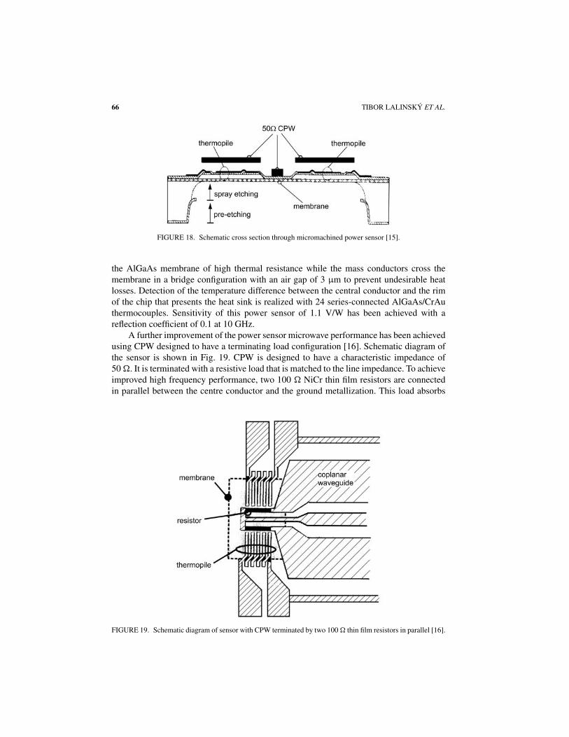
A new MMIC compatible sensor that measures RF and microwave power transmittedover a 50 � coplanar waveguide (CPW) was presented [15]. A schematic cross-sectionthrough the power sensor is shown in Fig. 18. It consists of CPW that feeds the RF powerto the sensor and an AlGaAs based thermopile that is proposed to measure the temperatureincrease. Both devices are integrated on a thin AlGaAs membrane. Back side bulk GaAsmicromachining based on spray etching with NH3OH/H2O2 solution was used to form a 1μm thick undoped Al0.48Ga0.52As membrane. The etching technique has the advantage ofhigh selectivity against Al0.48Ga0.52As while etching GaAs isotropically.
The sensor principle is based on the conversion of electrical power into heat resultingin a local temperature increase. Conversion is achieved via ohmic losses of the centralconductor of the CPW, which is an intrinsic effect of the CPW and hence should not affectits performance. The heat losses are converted into measurable temperature differencesby isolating the measurement region thermally. The central conductor is guided across
66 TIBOR LALINSKY ET AL.
FIGURE 18. Schematic cross section through micromachined power sensor [15].
the AlGaAs membrane of high thermal resistance while the mass conductors cross themembrane in a bridge configuration with an air gap of 3 μm to prevent undesirable heatlosses. Detection of the temperature difference between the central conductor and the rimof the chip that presents the heat sink is realized with 24 series-connected AlGaAs/CrAuthermocouples. Sensitivity of this power sensor of 1.1 V/W has been achieved with areflection coefficient of 0.1 at 10 GHz.
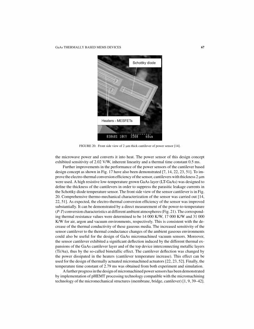
A further improvement of the power sensor microwave performance has been achievedusing CPW designed to have a terminating load configuration [16]. Schematic diagram ofthe sensor is shown in Fig. 19. CPW is designed to have a characteristic impedance of50 �. It is terminated with a resistive load that is matched to the line impedance. To achieveimproved high frequency performance, two 100 � NiCr thin film resistors are connectedin parallel between the centre conductor and the ground metallization. This load absorbs
FIGURE 19. Schematic diagram of sensor with CPW terminated by two 100 � thin film resistors in parallel [16].
GaAs THERMALLY BASED MEMS DEVICES 67
FIGURE 20. Front side view of 2 μm thick cantilever of power sensor [14].
the microwave power and converts it into heat. The power sensor of this design conceptexhibited sensitivity of 2.02 V/W, inherent linearity and a thermal time constant 0.5 ms.
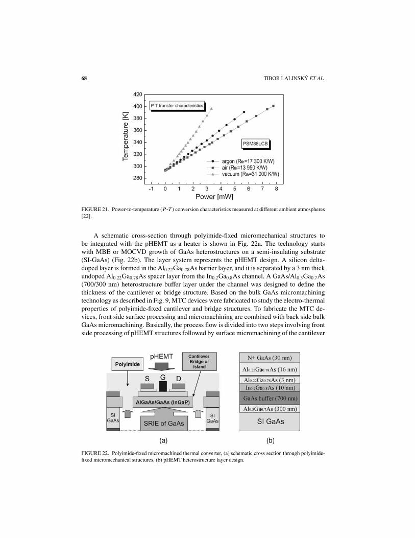
Further improvements in the performance of the power sensors of the cantilever baseddesign concept as shown in Fig. 17 have also been demonstrated [7, 14, 22, 23, 51]. To im-prove the electro-thermal conversion efficiency of the sensor, cantilevers with thickness 2μmwere used. A high resistive low-temperature grown GaAs layer (LT-GaAs) was designed todefine the thickness of the cantilevers in order to suppress the parasitic leakage currents inthe Schottky diode temperature sensor. The front side view of the sensor cantilever is in Fig.20. Comprehensive thermo-mechanical characterization of the sensor was carried out [14,22, 51]. As expected, the electro-thermal conversion efficiency of the sensor was improvedsubstantially. It can be demonstrated by a direct measurement of the power-to-temperature(P-T) conversion characteristics at different ambient atmospheres (Fig. 21). The correspond-ing thermal resistance values were determined to be 14 000 K/W, 17 000 K/W and 31 000K/W for air, argon and vacuum environments, respectively. This is consistent with the de-crease of the thermal conductivity of these gaseous media. The increased sensitivity of thesensor cantilever to the thermal conductance changes of the ambient gaseous environmentscould also be useful for the design of GaAs micromachined vacuum sensors. Moreover,the sensor cantilever exhibited a significant deflection induced by the different thermal ex-pansions of the GaAs cantilever layer and of the top device interconnecting metallic layers(Ti/Au), thus by the so-called bimetallic effect. The cantilever deflection was changed bythe power dissipated in the heaters (cantilever temperature increase). This effect can beused for the design of thermally actuated micromachined actuators [22, 23, 52]. Finally, thetemperature time constant of 2.79 ms was obtained from both experiment and simulation.
A further progress in the design of micromachined power sensors has been demonstratedby implementation of pHEMT processing technology compatible with the micromachiningtechnology of the micromechanical structures (membrane, bridge, cantilever) [1, 9, 39–42].
68 TIBOR LALINSKY ET AL.
FIGURE 21. Power-to-temperature (P-T ) conversion characteristics measured at different ambient atmospheres
[22].
A schematic cross-section through polyimide-fixed micromechanical structures tobe integrated with the pHEMT as a heater is shown in Fig. 22a. The technology startswith MBE or MOCVD growth of GaAs heterostructures on a semi-insulating substrate(SI-GaAs) (Fig. 22b). The layer system represents the pHEMT design. A silicon delta-doped layer is formed in the Al0.22Ga0.78As barrier layer, and it is separated by a 3 nm thickundoped Al0.22Ga0.78As spacer layer from the In0.2Ga0.8As channel. A GaAs/Al0.3Ga0.7As(700/300 nm) heterostructure buffer layer under the channel was designed to define thethickness of the cantilever or bridge structure. Based on the bulk GaAs micromachiningtechnology as described in Fig. 9, MTC devices were fabricated to study the electro-thermalproperties of polyimide-fixed cantilever and bridge structures. To fabricate the MTC de-vices, front side surface processing and micromachining are combined with back side bulkGaAs micromachining. Basically, the process flow is divided into two steps involving frontside processing of pHEMT structures followed by surface micromachining of the cantilever
FIGURE 22. Polyimide-fixed micromachined thermal converter, (a) schematic cross section through polyimide-
fixed micromechanical structures, (b) pHEMT heterostructure layer design.
GaAs THERMALLY BASED MEMS DEVICES 69
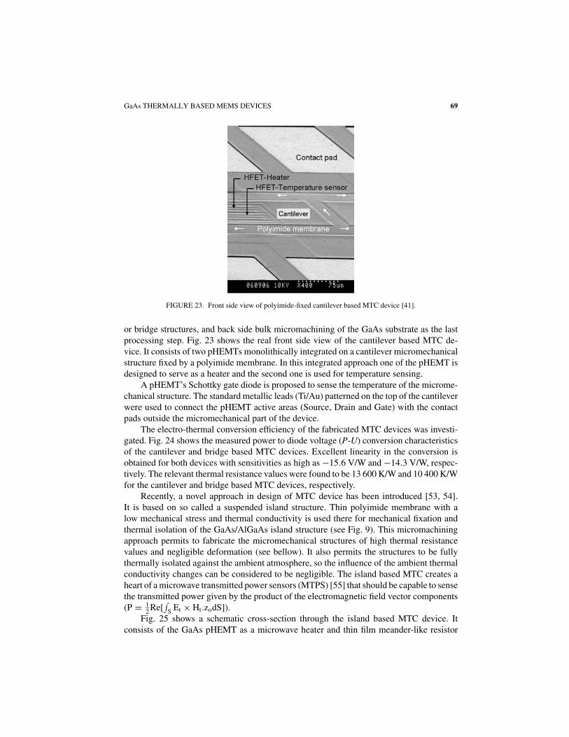
FIGURE 23. Front side view of polyimide-fixed cantilever based MTC device [41].
or bridge structures, and back side bulk micromachining of the GaAs substrate as the lastprocessing step. Fig. 23 shows the real front side view of the cantilever based MTC de-vice. It consists of two pHEMTs monolithically integrated on a cantilever micromechanicalstructure fixed by a polyimide membrane. In this integrated approach one of the pHEMT isdesigned to serve as a heater and the second one is used for temperature sensing.
A pHEMT’s Schottky gate diode is proposed to sense the temperature of the microme-chanical structure. The standard metallic leads (Ti/Au) patterned on the top of the cantileverwere used to connect the pHEMT active areas (Source, Drain and Gate) with the contactpads outside the micromechanical part of the device.
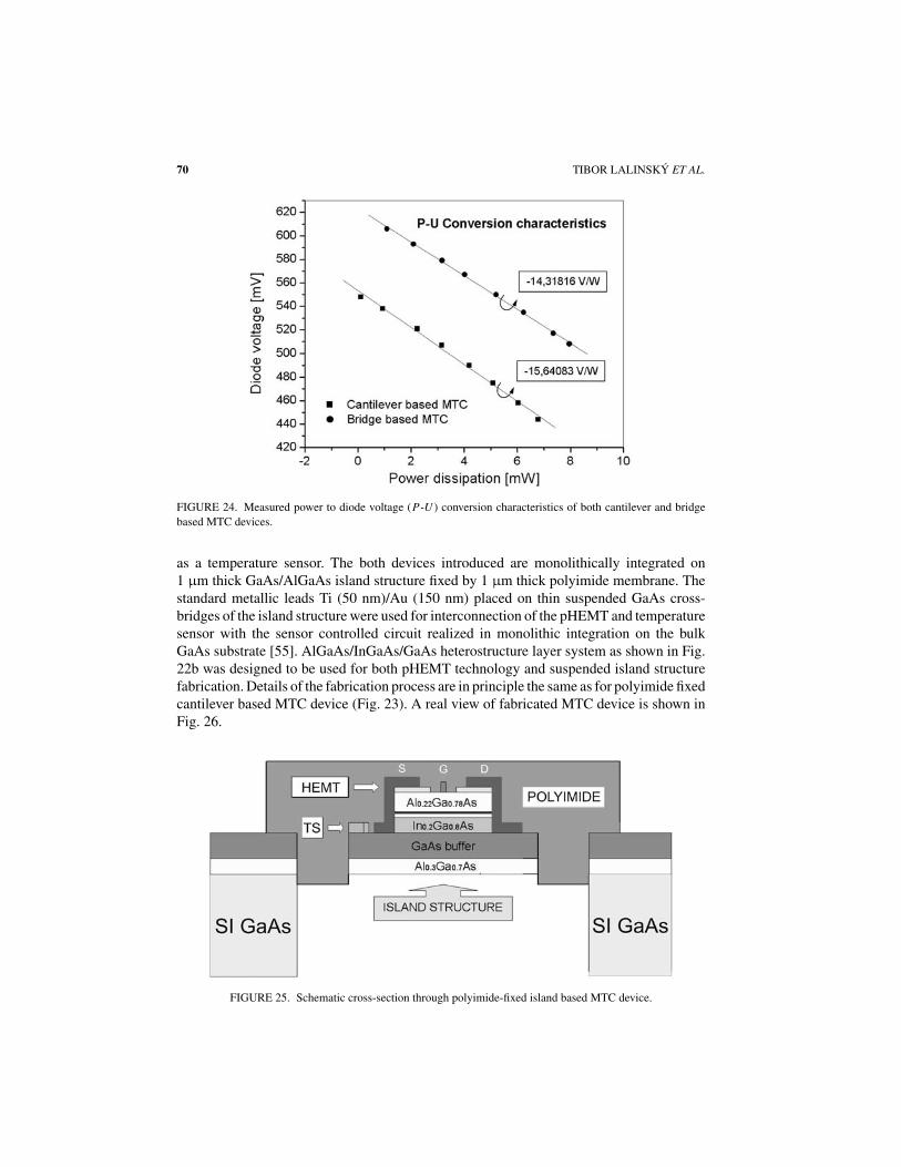
The electro-thermal conversion efficiency of the fabricated MTC devices was investi-gated. Fig. 24 shows the measured power to diode voltage (P-U) conversion characteristicsof the cantilever and bridge based MTC devices. Excellent linearity in the conversion isobtained for both devices with sensitivities as high as −15.6 V/W and −14.3 V/W, respec-tively. The relevant thermal resistance values were found to be 13 600 K/W and 10 400 K/Wfor the cantilever and bridge based MTC devices, respectively.
Recently, a novel approach in design of MTC device has been introduced [53, 54].It is based on so called a suspended island structure. Thin polyimide membrane with alow mechanical stress and thermal conductivity is used there for mechanical fixation andthermal isolation of the GaAs/AlGaAs island structure (see Fig. 9). This micromachiningapproach permits to fabricate the micromechanical structures of high thermal resistancevalues and negligible deformation (see bellow). It also permits the structures to be fullythermally isolated against the ambient atmosphere, so the influence of the ambient thermalconductivity changes can be considered to be negligible. The island based MTC creates aheart of a microwave transmitted power sensors (MTPS) [55] that should be capable to sensethe transmitted power given by the product of the electromagnetic field vector components(P = 1
2Re[
∫S
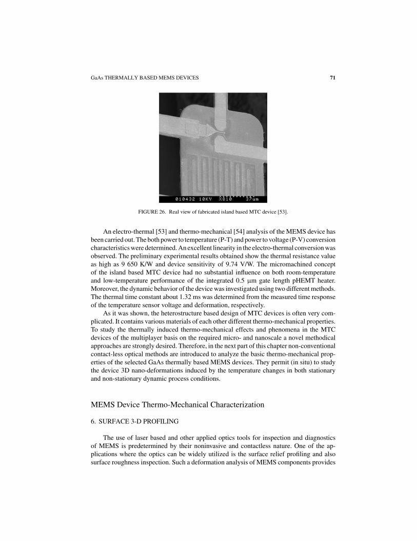
Et × Ht.zodS]).Fig. 25 shows a schematic cross-section through the island based MTC device. It
consists of the GaAs pHEMT as a microwave heater and thin film meander-like resistor
70 TIBOR LALINSKY ET AL.
FIGURE 24. Measured power to diode voltage (P-U ) conversion characteristics of both cantilever and bridge
based MTC devices.
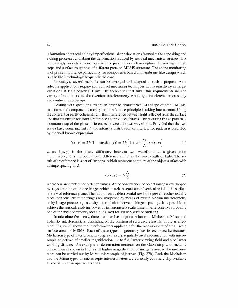
as a temperature sensor. The both devices introduced are monolithically integrated on1 μm thick GaAs/AlGaAs island structure fixed by 1 μm thick polyimide membrane. Thestandard metallic leads Ti (50 nm)/Au (150 nm) placed on thin suspended GaAs cross-bridges of the island structure were used for interconnection of the pHEMT and temperaturesensor with the sensor controlled circuit realized in monolithic integration on the bulkGaAs substrate [55]. AlGaAs/InGaAs/GaAs heterostructure layer system as shown in Fig.22b was designed to be used for both pHEMT technology and suspended island structurefabrication. Details of the fabrication process are in principle the same as for polyimide fixedcantilever based MTC device (Fig. 23). A real view of fabricated MTC device is shown inFig. 26.
FIGURE 25. Schematic cross-section through polyimide-fixed island based MTC device.
GaAs THERMALLY BASED MEMS DEVICES 71
FIGURE 26. Real view of fabricated island based MTC device [53].
An electro-thermal [53] and thermo-mechanical [54] analysis of the MEMS device hasbeen carried out. The both power to temperature (P-T) and power to voltage (P-V) conversioncharacteristics were determined. An excellent linearity in the electro-thermal conversion wasobserved. The preliminary experimental results obtained show the thermal resistance valueas high as 9 650 K/W and device sensitivity of 9.74 V/W. The micromachined conceptof the island based MTC device had no substantial influence on both room-temperatureand low-temperature performance of the integrated 0.5 μm gate length pHEMT heater.Moreover, the dynamic behavior of the device was investigated using two different methods.The thermal time constant about 1.32 ms was determined from the measured time responseof the temperature sensor voltage and deformation, respectively.
As it was shown, the heterostructure based design of MTC devices is often very com-plicated. It contains various materials of each other different thermo-mechanical properties.To study the thermally induced thermo-mechanical effects and phenomena in the MTCdevices of the multiplayer basis on the required micro- and nanoscale a novel methodicalapproaches are strongly desired. Therefore, in the next part of this chapter non-conventionalcontact-less optical methods are introduced to analyze the basic thermo-mechanical prop-erties of the selected GaAs thermally based MEMS devices. They permit (in situ) to studythe device 3D nano-deformations induced by the temperature changes in both stationaryand non-stationary dynamic process conditions.
MEMS Device Thermo-Mechanical Characterization
6. SURFACE 3-D PROFILING
The use of laser based and other applied optics tools for inspection and diagnosticsof MEMS is predetermined by their noninvasive and contactless nature. One of the ap-plications where the optics can be widely utilized is the surface relief profiling and alsosurface roughness inspection. Such a deformation analysis of MEMS components provides
72 TIBOR LALINSKY ET AL.
information about technology imperfections, shape deviations formed at the depositing andetching processes and about the deformation induced by residual mechanical stresses. It isincreasingly important to measure surface parameters such as coplanarity, warpage. heighsteps and surface roughness of different parts on MEMS structure. The shape monitoringis of prime importance particularly for components based on membrane-like design whichis in MEMS technology frequently the case.
Nowadays, several methods can be arranged and adapted to such a purpose. As arule, the applications require non-contact measuring techniques with a sensitivity in heightvariations at least bellow 0.1 μm. The techniques that fulfill this requirements includevariety of modifications of convenient interferometry, white light interference microscopyand confocal microscopy.
Dealing with specular surfaces in order to characterize 3-D shape of small MEMSstructures and components, mostly the interference principle is taking into account. Usingthe coherent or partly coherent light, the interference between light reflected from the surfaceand that returned back from a reference flat produces fringes. The resulting fringe pattern isa contour map of the phase differences between the two wavefronts. Provided that the twowaves have equal intensity I0 the intensity distribution of interference pattern is describedby the well known expression
I (x, y) = 2I0[1 + cos δ(x, y)] = 2I0
[1 + cos
2π
�z(x, y)
](1)
where δ(x, y) is the phase difference between two wavefronts at a given point(x, y), z(x, y) is the optical path difference and Λ is the wavelength of light. The re-sult of interference is a set of “fringes” which represent contours of the object surface witha fringe spacing of Λ
z(x, y) = N�
2(2)
where N is an interference order of fringes. At the observation the object image is overlappedby a system of interference fringes which match the contours of vertical relief of the surfacein view of reference plane. The ratio of vertical/horizontal resolving power reaches usuallymore than tens, but if the fringes are sharpened by means of multiple-beam interferometryor by image processing intensity interpolation between fringes spacings, it is possible toachieve the vertical resolving power up to nanometers scale. Laser interferometry is probablyone of the most commonly techniques used for MEMS surface profiling.
In microinterferometry, there are three basic optical schemes—Michelson, Mirau andTolansky interferometers, depending on the position of reference glass flat in the arrange-ment. Figure 27 shows the interferometers applicable for the measurement of small scalesurface areas of MEMS. Each of these types of geometry has its own specific features.Michelson type of interferometer (Fig. 27a) is e.g. regularly used in connection with micro-scopic objectives of smaller magnification 1× to 5×, larger viewing field and also largerworking distance. An example of deformation contours on the GaAs strip with metallicconnections is shown in Fig. 28. If higher magnification of image is needed the measure-ment can be carried out by Mirau microscopic objectives (Fig. 27b). Both the Michelsonand the Mirau types of microscopic interferometers are currently commercially availableas special microscopic accessories.
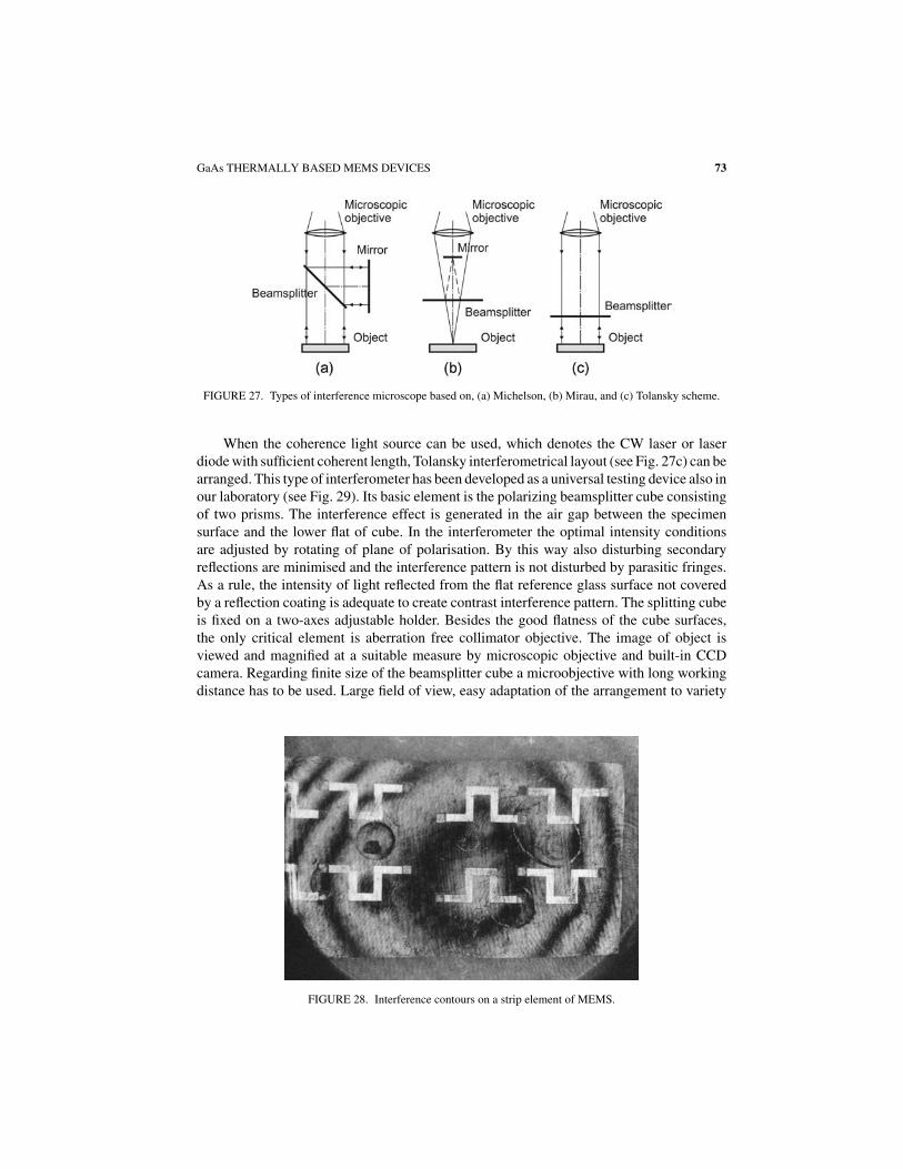
GaAs THERMALLY BASED MEMS DEVICES 73
FIGURE 27. Types of interference microscope based on, (a) Michelson, (b) Mirau, and (c) Tolansky scheme.
When the coherence light source can be used, which denotes the CW laser or laserdiode with sufficient coherent length, Tolansky interferometrical layout (see Fig. 27c) can bearranged. This type of interferometer has been developed as a universal testing device also inour laboratory (see Fig. 29). Its basic element is the polarizing beamsplitter cube consistingof two prisms. The interference effect is generated in the air gap between the specimensurface and the lower flat of cube. In the interferometer the optimal intensity conditionsare adjusted by rotating of plane of polarisation. By this way also disturbing secondaryreflections are minimised and the interference pattern is not disturbed by parasitic fringes.As a rule, the intensity of light reflected from the flat reference glass surface not coveredby a reflection coating is adequate to create contrast interference pattern. The splitting cubeis fixed on a two-axes adjustable holder. Besides the good flatness of the cube surfaces,the only critical element is aberration free collimator objective. The image of object isviewed and magnified at a suitable measure by microscopic objective and built-in CCDcamera. Regarding finite size of the beamsplitter cube a microobjective with long workingdistance has to be used. Large field of view, easy adaptation of the arrangement to variety
FIGURE 28. Interference contours on a strip element of MEMS.

74 TIBOR LALINSKY ET AL.
FIGURE 29. Microinterferometrical setup based on Tolansky optical scheme.
of purposes and also the possibility of simultaneous observation of thin film interferencepattern on transparent surface covering are the practical advantages of the device.
Several kinds of components made of GaAs based technology of membrane-like struc-tures has been tested using this tool [14, 19, 25, 41, 42]. In Fig. 30 the interferometricallymeasured profiles along the length of free cantilever are drawn. As it can be seen, besidesthe visualisation of steady-state profile of the cantilever after its technological forming, thechanges generated as a thermal response by acting feeding power has been inspected, too.
Another alternative of Tolansky arrangement is the reference flat positioned by layingit on the measured surface or in its vicinity. If this flat is kept at a small angle to the surfacemean level then the set of profiles is created. In this case the interpretation of fringe pattern isnot so clear and straightforward comparing the height contour fringes presented by previousschemes, nevertheless, the shape of surface can be computed too, from the data of fringepattern viewed by a CCD camera. One of the advantages of this adjustment is the possibility
FIGURE 30. Steady-state profiles of cantilever deflection as a function of power dissipation [25].
GaAs THERMALLY BASED MEMS DEVICES 75
of simple varying of sensitivity in line-of-sight direction. This interferometry is especiallyusefull when the surface defects diagnostics is necessary.
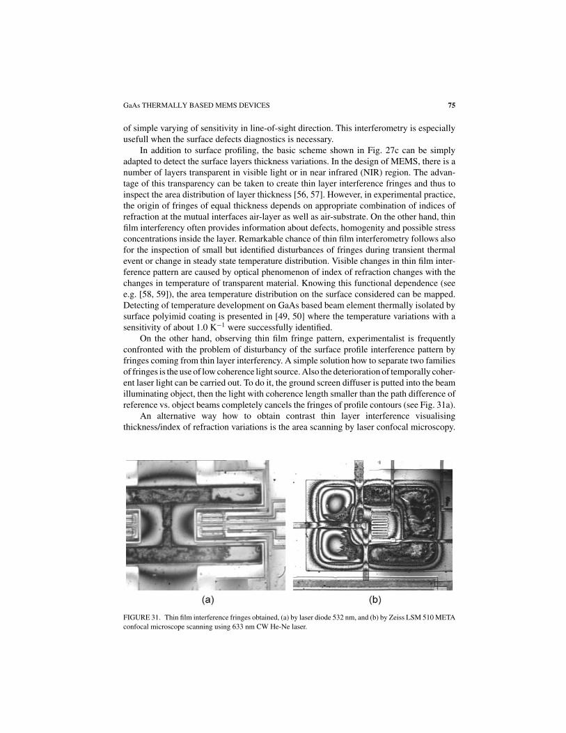
In addition to surface profiling, the basic scheme shown in Fig. 27c can be simplyadapted to detect the surface layers thickness variations. In the design of MEMS, there is anumber of layers transparent in visible light or in near infrared (NIR) region. The advan-tage of this transparency can be taken to create thin layer interference fringes and thus toinspect the area distribution of layer thickness [56, 57]. However, in experimental practice,the origin of fringes of equal thickness depends on appropriate combination of indices ofrefraction at the mutual interfaces air-layer as well as air-substrate. On the other hand, thinfilm interferency often provides information about defects, homogenity and possible stressconcentrations inside the layer. Remarkable chance of thin film interferometry follows alsofor the inspection of small but identified disturbances of fringes during transient thermalevent or change in steady state temperature distribution. Visible changes in thin film inter-ference pattern are caused by optical phenomenon of index of refraction changes with thechanges in temperature of transparent material. Knowing this functional dependence (seee.g. [58, 59]), the area temperature distribution on the surface considered can be mapped.Detecting of temperature development on GaAs based beam element thermally isolated bysurface polyimid coating is presented in [49, 50] where the temperature variations with asensitivity of about 1.0 K−1 were successfully identified.
On the other hand, observing thin film fringe pattern, experimentalist is frequentlyconfronted with the problem of disturbancy of the surface profile interference pattern byfringes coming from thin layer interferency. A simple solution how to separate two familiesof fringes is the use of low coherence light source. Also the deterioration of temporally coher-ent laser light can be carried out. To do it, the ground screen diffuser is putted into the beamilluminating object, then the light with coherence length smaller than the path difference ofreference vs. object beams completely cancels the fringes of profile contours (see Fig. 31a).
An alternative way how to obtain contrast thin layer interference visualisingthickness/index of refraction variations is the area scanning by laser confocal microscopy.
FIGURE 31. Thin film interference fringes obtained, (a) by laser diode 532 nm, and (b) by Zeiss LSM 510 META
confocal microscope scanning using 633 nm CW He-Ne laser.
76 TIBOR LALINSKY ET AL.
In Fig. 31b thin layer interferency is illustrated on surface polyimid film with the thicknessof about 1 μm. By this polyimid the membrane structure of GaAs/AlGaAs island element,slits between the island and the bulk within the area of clearly visible boundaries are cov-ered, and the reflection from back and front side and subsequent interference of confocalmicroscope probing light creates the thin film interference fringes. Mechanism of theirforming follows from confocal microscope SW processing procedures where pixel-to-pixeldepth intensity profiles are processed for searching the best maximum intensity positions,thus visualising the localization of both destructive and constructive interferency. As seen,the fringes visualises also defects caused by imperfections of etching process and polyimidlayer depositing. The layer thickness distribution reflects the influence of capillarity and/orshrinkage effects at edges and corners.
Low coherence or white light interference microscope [60–63] is an advanced toolwith some specific advantages over the “conventional” interferometric technique [60, 64].It is primarily the ability to strongly reject light that has undergone scattering outside whichgives the generation of speckles when illuminating by coherent light. When a low coherencelight is used in interference microscope, and the microscope objective is moved continouslyin line-of-sight axis, the contrast of interference fringes is modulated depending upon theoptical path difference. A low coherence interferogram can be described by a constant meanintensity I0 and a series of sinusoidal fringes modulated by envelope function [60]
I (x, y) = I0(x, y)[1 + V (x, y, �) cos �] (3)
where the function V (x, y, Φ) is the visibility or fringe contrast, which varies much moreslowly with optical path difference than the fringe phase Φ = Φ(x, y). A basic principle isthe searching for the position of maximum contrast simultaneously for an array of imagepoints. Thus, a 3-D surface profile can be measured by finding the maximum peak positionof the fringes modulation in a CCD camera. At present, there have been many approachesof calculation algorithms to find this maximum as reliably and precisely as possible and ina shortest time. Modern white light interference microscopes are typically equipped withMirau objective and a moderately filtered white light source is halogen lamp or high bright-ness LED. The interference fringes envelope has a width of some micrometers, hence theaccuracy of measurements can be defined as tens of nanometers. Last years the applicationsof white light interferometry to MEMS/MOEMS devices testing have become increasinglyimportant.
Sometimes the interferometric technique cannot be applied for surface geometry profil-ing, for example, when the surface is optically rough and reflects the light diffusely. Problemsolution in this case can be application of confocal microscopy [65–67]. Convenient con-focal microscopy belongs to large group of optical techniques involving lateral mechanicalscanning as part of the 3-D data acquisition. In optical scheme of confocal microscope,light of point-like source is projected into the object focal plane of microscope objective.The light reflected backward is collected by the same objective and after passing throughthe beamsplitter it is projected onto a detector pinhole. Only the focused positions of thesample surface give the maximum signals and light is strongly reduced by pinhole whenthe surface is in defocused position. In this manner the plane of best focusing is definedand three coordinates location of measuring point is recognised. The lateral resolution of3-D profiling is related to the smallest spot diameter d that follows from the Airy disc
GaAs THERMALLY BASED MEMS DEVICES 77
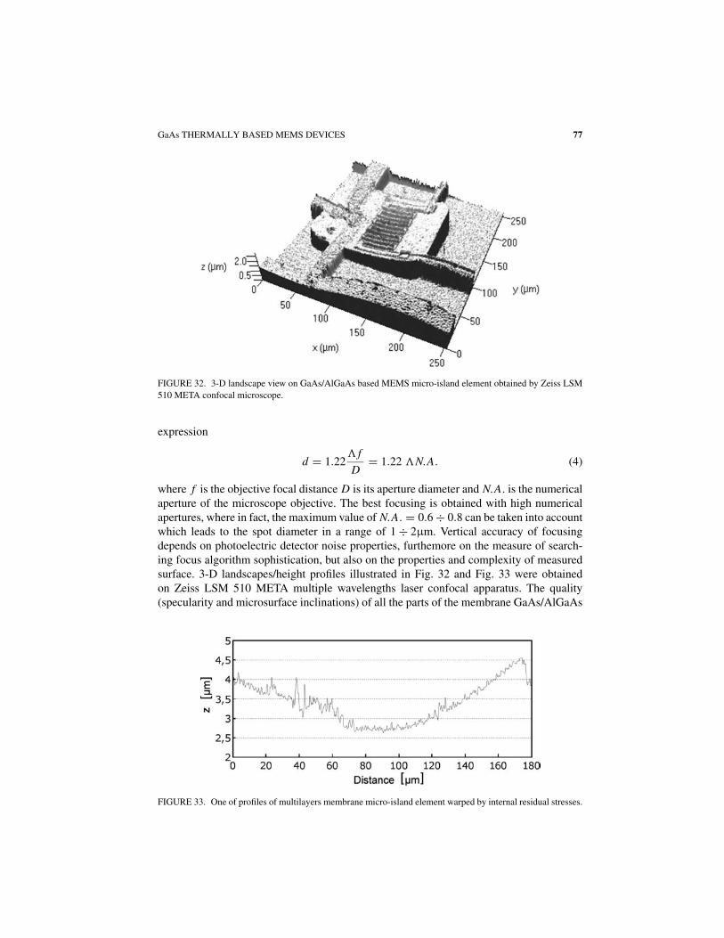
FIGURE 32. 3-D landscape view on GaAs/AlGaAs based MEMS micro-island element obtained by Zeiss LSM
510 META confocal microscope.
expression
d = 1.22� f
D= 1.22 �N.A. (4)
where f is the objective focal distance D is its aperture diameter and N.A. is the numericalaperture of the microscope objective. The best focusing is obtained with high numericalapertures, where in fact, the maximum value of N.A. = 0.6 ÷ 0.8 can be taken into accountwhich leads to the spot diameter in a range of 1 ÷ 2μm. Vertical accuracy of focusingdepends on photoelectric detector noise properties, furthemore on the measure of search-ing focus algorithm sophistication, but also on the properties and complexity of measuredsurface. 3-D landscapes/height profiles illustrated in Fig. 32 and Fig. 33 were obtainedon Zeiss LSM 510 META multiple wavelengths laser confocal apparatus. The quality(specularity and microsurface inclinations) of all the parts of the membrane GaAs/AlGaAs
FIGURE 33. One of profiles of multilayers membrane micro-island element warped by internal residual stresses.
78 TIBOR LALINSKY ET AL.
microisland MEMS surface has not been uniform and scanning of the MEMS devicerequired retrieving of optimal working wavelength of light, appropriate algorithm of focalposition detecting and also the choise of suitable parameters of microobjectives used. As itwas noticed above, for some specimens covered with polyimid, the thin layer interferencyhas appeared and excluded proper interpretation of primary recorded data of depth intensityprofiles. In this case the problem has been eliminated by processing and following averagingof the data acquired by using of different light wavelengths. As it can be assessed also fromthe one of the cross-section profiles at the real mirror-like parts, the standard deviation σ isless than 0.1 μm, the value frequently cited for confocal microscopy.
7. DETERMINATION OF GaAs/AlGaAs MATERIAL PARAMETERS
At the designing process of the MEMS device the knowledge of structural mechanicalstress state is often essential to the right weighting of all the mechanical proposal aspects.Nowadays, the development and fabrication of MEMS devices especially based on GaAstechnology, has not been realized using only conventional well established proceduresand known material parameters. Increasing design and performance demands in the nearfuture will require more exact and complete information considering both the mechanicaland thermo-mechanical materials properties and their mutual interactions in multilayersystem. It is well known that most of convenient mechanical test techniques and procedureswere developed to bulk materials and are not generally suitable for thin film applications.Therefore, new or modified methods has to be elaborated.
The basic requirement of any test used to gather information about materials parametersis an application of controllable externally applied loading and measurement of deformationresponse (static or dynamic) of mechanical components to this actuation. It can be notedthat the most widely used techniques of deformation measurements on microcomponentsare the methods where the applied optics principles are employed. The techniques can beapplied such as interferometry, electronic speckle pattern interferometry (ESPI), point-likelaser reflectance measurement or the measurement by autocollimation arrangement wherethe light reflected from the object is analysed in or nearly back focal plane of imaging lens.Besides more or less convenient microtensile testing, when the CCD camera or ESPI areused for deformation tracking, a free-standing thin film beam is bended to plot materialloading diagram and subsequent elastic moduli extraction. Regularly used vibrational (orresonant) testing is a variation of the latter method.
Another widely used procedure of Young’s modulus and membrane tension stressmeasurement is the method usually called as bulging test. In this case, the membranecomponent is deformed by applying one-side overpressure. Provided that t is the thicknessof the membrane, a is the lateral size and w is the central deflection of bulged membraneinduced by overpressure p, it can be writen [68]
p(w) = K1
σ t
a2w + K2(v)
Et
a4w3 (5)
where E and σ are the elastic modulus and the membrane tension stress, respectively. Theconstants K1, K2 depend only on the lateral geometry of membrane component. Optical
GaAs THERMALLY BASED MEMS DEVICES 79
detection of current value w can be effectively accomplished by the whole viewing fieldobservation, interferometrically or by autocollimation searching shifted focus.
8. RESIDUAL STRESS ANALYSIS
The presence of residual stresses is a characteristic feature of almost all the multilayeredstructures composed of different materials. The residual stress result from heterogenity ofmaterial properties and from treatment by thermal but also by mechanical means. The lastgroup can be often identified e.g. after grinding and finishing a mirror-like GaAs (or Si)wafer front side area. The mechanical intervency (or chemical when chemical polishing isapplied) affects upper layers of the single crystalline material whose microstructure tends tofollow predominantly its crystallographic structure. This phenomenon is visible on almostall the maiden polished surfaces of wafers at the inspection of initial wafer deformation.The surface flatness curving either large-scale or only negligible, shows ellipsoidal shape,and sometimes even saddle-like warping, with the main axes of symmetry in accordancewith orthogonal axes of monocrystal.
However, in fabrication processes the main role play the residual stress state the originof what is the different thermal dilatability of coating and substrate and intrinsic mutualinteraction, both inherent practically in all of the deposition processes. As it is known, theorigin and nature of internal residual stresses are the sources of many mechanical effectsin coatings and repeatedly are of prime concern when dealing with multilayer complicatedsystem.
Experimental detection and evaluation of residual stresses can be divided into twocategories:
i/ measurement of steady state deformation induced by residual stress in free-standingstructural elements
ii/ measurement of deformation forced to clamped thin plate or membrane-like ele-ments by controllable loading
The well known measurement of film stresses of coated wafers belongs into the formercategory where the coating film stress is determined by measurement of wafer thin platefree deformation. The method is appropriate if interaction between film and substrate isnecessary to know and the conditions of depositing process can be simulated, identical withthat used at actual fabrication of designed MEMS device. Assuming the homogeneous stressdistribution throughout the wafer area, the relationship between the searched film stress andthe induced deformation is very simple, described by Stoney formula (see bellow). Theonly one parameter which has to be determined in this case, is the radius of curvature ofspherically bulged substrate.
In principle, this small spherical deformation of the wafer surface can be accomplishedby a number of optical methods. The presence of the specular surface makes the task rel-atively simple to solve from the point of view of optical techniques, testing arrangementcan be materialised by classic means. In a market, several measurement systems commer-cially available are intended to such a purposes [69, 70]. The systems of KLA Tencor areespecially adapted to the thermal stress evaluation and are even equipped with a thermallycontrolled testing chamber.

80 TIBOR LALINSKY ET AL.
In spite of that, the automated systems are not always matched with the varying require-ments of designing researcher. Therefore, the comparative analysis has been performed ofseveral optical techniques under consideration [71, 72]. Apart from the using of convenientinterferometry, common drawback of which is frequently its even excessive sensitivity, andthe need to use large precise optical elements, a holographic interferometry setup has beenrealised. One of the main attractions of holographic interferometry is the comparative princi-ple, attribute that can be exploited to separate of initial flatness distortions. Such distortionsmany times are not spherically shaped and as it has to be noted, the value of deformationoften is of the same order as that induced by thermal/intrinsic stresses. The advantage ofholographic direct optical differential mode of measurement has proved particularly whenthe small deformation changes are needed to be determined. Practical drawbacks of holog-raphy, mainly its technical realization, has been overcome by installing of electronic specklepattern interferometry (ESPI) with PC based image processing.
Another optical principle tested was a specific variant of classic Ronchi’s ruling setup.In the method with no moving components and no large glass prisms and mirrors (withextention of large diameter abberation free doublet of objective lens) a coarse grid positionedat back focal plane is used. The rays reflected from the specular object are collected at thefocal plane and are passing through the coarse (1 ÷ 5 lines per mm) grid. The grid, in factbinary filter of optical filtration scheme, is projected onto the screen in a view of fringesvisualising slope contours of the surface tested.
Among simple and unpretending optical scheme realisations, a method of autocollima-tion or searching focus, can also be named [73]. As it was mentioned above, the inspection ofthin layer residual stresses on wafers requires only information about the radius of curvatureof the approximatelly spherical surface. Similarly as in the previous technique of slope con-tours, the beam of parallel rays is reflected from polished surface (see Fig. 34). In the case ofreflection from flat surface the light after passing backward through the long focal distance(about 1 m) objective is concentrated precisely into focal plane. The change of reflectedarea to spherical shape (concave or convex) will shift the “focus” spot along optical axis outof initial position. The focus shift is measured to determine the value of surface curvatureR related with the shift by a simple formula derived by elementary ray tracing laws
R = 2
(f 2
+ f − l
)(6)
where f is the focal distance of objective lens and l is the mutual distance objective—specimen. Generally, in the case of orthogonally symmetric surface which is on wafers
FIGURE 34. Optical scheme of wafers curvature measurement based on autocollimation principle.
GaAs THERMALLY BASED MEMS DEVICES 81
often the case, the reflected light will form an astigmatic beam. As it is known [56], twoplanes which contain the shortest and the longest radius of curvature, are perpendicularto each other. The corresponding curvatures are usually called tangential field of curvatureRT and sagittal field curvature RS . The quantity
1
R= 1
2
(1
RT+ 1
RS
)(7)
is their arithmetic mean value. Both the radii RT and RS can be determined experimentally,by searching for tangential as well as sagittal focal line spots. The information whetherthe measured curvature is concave or convex is defined by direction of focal spot shifting(toward or from the objective lens).
When speaking about the measurement sensitivity, such an autocollimation scheme isat the same level as interferometrical surface contour fringe pattern, moreover, also in thismethod in principle, photoelectric or CCD based focal spot position detection can easy beinstalled. The accuracy of the measurement is sufficient for reliable determination of residualstresses even on the samples 10 ÷ 20 mm in diameter. The stresses can be determined withreasonable precission of several MPa in a large range of measurement up to 10 GPa. Oneadvancement more is the testing of materials, where their anisotropic properties have tobe accounted for. Simple separation and determination of orthogonal curvatures as well asusing of Eq. 7 provides good orientation in evaluation of orthotropic stress components [74].A number of thermal/intrinsic residual stress measurements has been reported elsewhere[75–77].
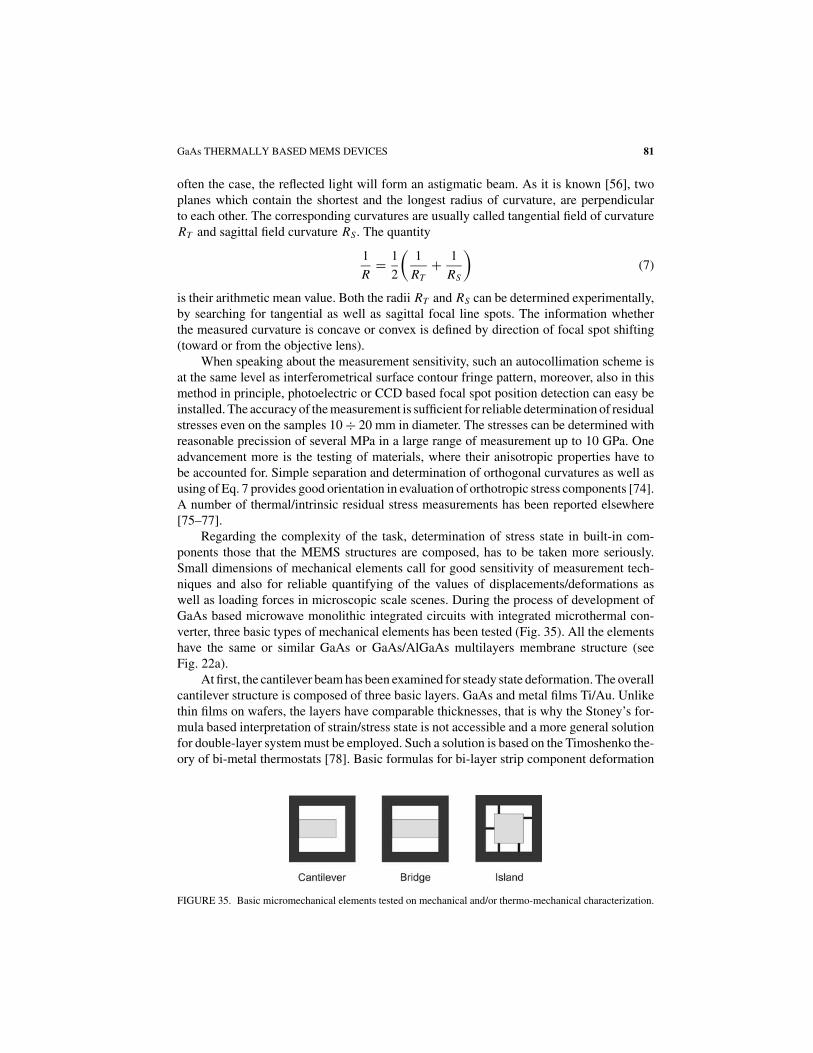
Regarding the complexity of the task, determination of stress state in built-in com-ponents those that the MEMS structures are composed, has to be taken more seriously.Small dimensions of mechanical elements call for good sensitivity of measurement tech-niques and also for reliable quantifying of the values of displacements/deformations aswell as loading forces in microscopic scale scenes. During the process of development ofGaAs based microwave monolithic integrated circuits with integrated microthermal con-verter, three basic types of mechanical elements has been tested (Fig. 35). All the elementshave the same or similar GaAs or GaAs/AlGaAs multilayers membrane structure (seeFig. 22a).
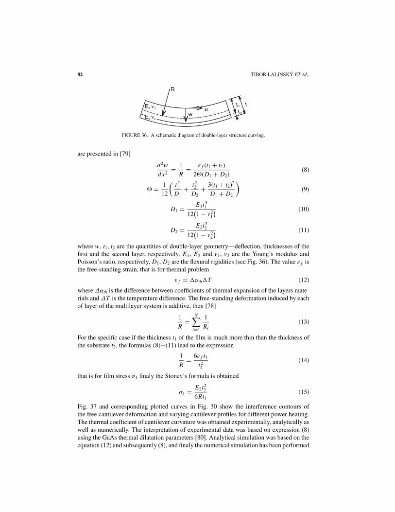
At first, the cantilever beam has been examined for steady state deformation. The overallcantilever structure is composed of three basic layers. GaAs and metal films Ti/Au. Unlikethin films on wafers, the layers have comparable thicknesses, that is why the Stoney’s for-mula based interpretation of strain/stress state is not accessible and a more general solutionfor double-layer system must be employed. Such a solution is based on the Timoshenko the-ory of bi-metal thermostats [78]. Basic formulas for bi-layer strip component deformation
FIGURE 35. Basic micromechanical elements tested on mechanical and/or thermo-mechanical characterization.
82 TIBOR LALINSKY ET AL.
FIGURE 36. A schematic diagram of double-layer structure curving.
are presented in [79]
d2w
dx2= 1
R= ε f (t1 + t2)
2�(D1 + D2)(8)
� = 1
12
(t21
D1
+ t22
D2
+ 3(t1 + t2)2
D1 + D2
)(9)
D1 = E1t31
12(1 − v2
1
) (10)
D2 = E2t32
12(1 − v2
2
) (11)
where w , t1, t2 are the quantities of double-layer geometry—deflection, thicknesses of thefirst and the second layer, respectively. E1, E2 and v1, v2 are the Young’s modulus andPoisson’s ratio, respectively, D1, D2 are the flexural rigidities (see Fig. 36). The value ε f isthe free-standing strain, that is for thermal problem
ε f = αthT (12)
where Δαth is the difference between coefficients of thermal expansion of the layers mate-rials and ΔT is the temperature difference. The free-standing deformation induced by eachof layer of the multilayer system is additive, then [78]
1
R=
N∑i=1
1
Ri(13)
For the specific case if the thickness t1 of the film is much more thin than the thickness ofthe substrate t2, the formulas (8)−(11) lead to the expression
1
R= 6ε f t1
t22
(14)
that is for film stress σ1 finaly the Stoney’s formula is obtained
σ1 = E2t22
6Rt1(15)
Fig. 37 and corresponding plotted curves in Fig. 30 show the interference contours ofthe free cantilever deformation and varying cantilever profiles for different power heating.The thermal coefficient of cantilever curvature was obtained experimentally, analytically aswell as numerically. The interpretation of experimental data was based on expression (8)using the GaAs thermal dilatation parameters [80]. Analytical simulation was based on theequation (12) and subsequently (8), and finaly the numerical simulation has been performed
GaAs THERMALLY BASED MEMS DEVICES 83
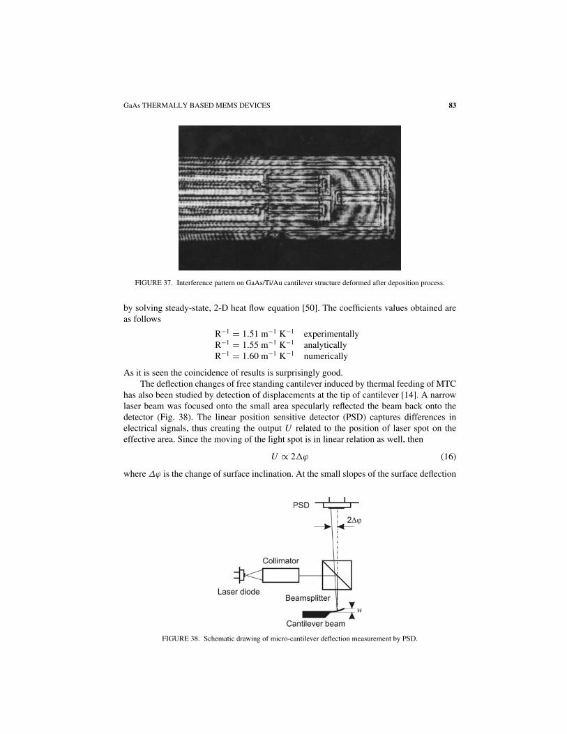
FIGURE 37. Interference pattern on GaAs/Ti/Au cantilever structure deformed after deposition process.
by solving steady-state, 2-D heat flow equation [50]. The coefficients values obtained areas follows
R−1 = 1.51 m−1 K−1 experimentallyR−1 = 1.55 m−1 K−1 analyticallyR−1 = 1.60 m−1 K−1 numerically
As it is seen the coincidence of results is surprisingly good.The deflection changes of free standing cantilever induced by thermal feeding of MTC
has also been studied by detection of displacements at the tip of cantilever [14]. A narrowlaser beam was focused onto the small area specularly reflected the beam back onto thedetector (Fig. 38). The linear position sensitive detector (PSD) captures differences inelectrical signals, thus creating the output U related to the position of laser spot on theeffective area. Since the moving of the light spot is in linear relation as well, then
U ∝ 2ϕ (16)
where Δϕ is the change of surface inclination. At the small slopes of the surface deflection
FIGURE 38. Schematic drawing of micro-cantilever deflection measurement by PSD.

84 TIBOR LALINSKY ET AL.
w is related to lateral coordinate x
U = K · 2dw
dx(17)
where K is the factor of proportionality—sensitivity value. At the experiment a good pro-portionality has been obtained in the relation deflection vs. heating power, in spite of con-siderable distortion of the reflected light spot upon the effective PSD area. It implies, thatthe accuracy of such a measurement is not affected strongly by this current effect. Anotherknowledge obtained was an excelent repeatability of the cantilever deformation changes.Such finding speaks in support of fact that the nature of residual stresses/ steady state de-formation is thermal dilatation. Potential intrinsic stresses are predominantly induced bymicrostructural changes of interfaced materials and their mutual diffusion, that is why as arule characteristic feature is their irreversibility during the thermal treating [81].
The Laser Doppler Vibrometer (LDV) is basically intended as a tool to measure peri-odic and, perhaps, stochastic vibrations, though the measurement principle of this techniquepermits its using for detection of one-shot events, too. Such an application has been carriedout in order to observe the dynamic behaviour of GaAs technology based membrane mi-croisland mechanical component (Fig. 35). At the experiments results of time dependentdeflection development has been studied as a reaction to input step-wise electric/heatingpower. The effect of mechanical deformation follows from the mismatch of coefficientsof thermal expansion. By the repeated loading the microisland area was mapped point bypoint to create a mesh of displacements perpendicular to the surface. Fig. 39a,b showsthe rising and falling parts of transient microisland deformation thermal response in oneof the points. In order to analyze the results measured we have taken into account as afirst approximation the linearly proportional relationship between the out-of-plane defor-mation and actual temperature at the point of inspection by LDV. The relation was demon-strated numerically and it can be seen also from the comparison of measured temperaturevs. time dependence on the thermal sensor as well. The latter assumption has led to thepossibility of thermal-time response evaluation of MTC by means of deformation ratesdetecting.
Experimental determination of internal residual stresses by well defined loading is im-portant particularly when the components or integrated parts of MEMS are fabricated as
FIGURE 39. Rising (a) and falling (b) branches of transient thermal response of membrane micro-island on
square-wave-shaped heat loading.

GaAs THERMALLY BASED MEMS DEVICES 85
membrane-like structures. Small dimensions of the mechanical components limit possibil-ities of tiny loading. Common, frequently used electrostatic mechanical exciting of staticdeformation as well as dynamic movings has inherent limitation consisting in a necessityof electric conductance of the surface to be loaded. Another approach is based on the em-ployment of different thermal dilatation of MEMS materials by their heating or cooling.The observation of similarly actuated double (or three) layer element has been mentionedabove. Besides the convenient heating the component under consideration can be heated bylaser light energy as well [82]. In order to perform the laser beam excitation, mostly pulsedlasers are used. Typically laser pulses of Nd-YAG source 532 nm or 1064 nm are appliedwith an energy of mJ or even less which are sufficient to excite the measurable mechanicalresponse. The energy of each pulse of short duration induces considerable increase of localsurface temperature which is immediately followed by localy induced thermal dilatation.The interest for this loading method in micromechanics has to be increasing because ofthe possibility to excite very small objects. Nevertheless, against expectation, as a maindrawbacks of the laser excitation may be regarded both badly controllable absolute valueof loading as well as rather invasive way of interaction with the specimen tested involvedin an eventual change of thermally dependent materials parameters.
Taking into account these opportunities and limitations, the loading through the acousti-cal coupling has been chosen to study the GaAs/AlGaAs membrane-like multilayer structureof microbridge (see above). The excitation of mechanical movement by sound can be re-garded as desirable because of its tenderness and simple handling with both intensity andfrequency adjusting. In vibrational analysis the acoustic excitation is currently used, how-ever, the usual problem has arised, if the quantifying of actuating acoustic pressure valueshas to be done. To overcome the problem a procedure has been developed of the precise de-termination of acoustic pressure emitting by loudspeaker membrane by membrane vibrationvelocities measurement. This, in fact absolute calibration, is based on relationship betweenthe velocity of longitudinally vibrating particles emitting by loudspeaker membrane andthe periodic harmonic pressure changes ps
ps = ρcsv (18)
where v is the velocity of vibrations, ρ is the air density and cs is sound velocity. In thenearest neighborhood of the vibrating loudspeaker membrane equal acoustic pressure can beadmitted. For plane wave of sound the acoustic pressure and acoustic velocity are in phasethat is Eq. (18) can be successfully applied to calculate the pressure. The use of Laser DopplerVibrometer (LDV) is an ideal manner how to precisely gauge the velocities of loudspeakermembrane vibration, hence, the value of acoustic pressure can be accurately determined.
Another way how to tackle the task of controllable sound exciting is a generationof periodic harmonic changes of uniform pressure under the membrane bridge in a smallchamber of pistonphone. Pistonphone is a device designed for microphone calibration andprovides nominal sound level pressure of 118 dB at 173 Hz. This value is related to 15.8Pa (RMS) of the acoustic pressure which is in the range of several Pa to tens of Pa mostlyadequate to experiments with micromechanical components.
Although the tension in a bridge membrane allows to be evaluated on the basis ofmeasured resonant frequencies, the first resonant mode occurs at region of 60 ÷ 100 kHzwhere the sound excitation is not very effective. On the other hand the expressive bulgingoscillations of the microbridge are present at low sound frequencies where the loudspeaker
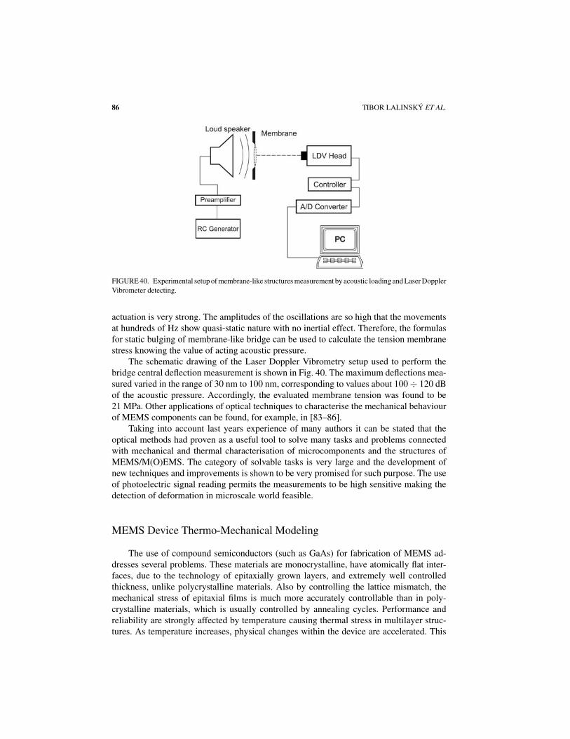
86 TIBOR LALINSKY ET AL.
FIGURE 40. Experimental setup of membrane-like structures measurement by acoustic loading and Laser Doppler
Vibrometer detecting.
actuation is very strong. The amplitudes of the oscillations are so high that the movementsat hundreds of Hz show quasi-static nature with no inertial effect. Therefore, the formulasfor static bulging of membrane-like bridge can be used to calculate the tension membranestress knowing the value of acting acoustic pressure.
The schematic drawing of the Laser Doppler Vibrometry setup used to perform thebridge central deflection measurement is shown in Fig. 40. The maximum deflections mea-sured varied in the range of 30 nm to 100 nm, corresponding to values about 100 ÷ 120 dBof the acoustic pressure. Accordingly, the evaluated membrane tension was found to be21 MPa. Other applications of optical techniques to characterise the mechanical behaviourof MEMS components can be found, for example, in [83–86].
Taking into account last years experience of many authors it can be stated that theoptical methods had proven as a useful tool to solve many tasks and problems connectedwith mechanical and thermal characterisation of microcomponents and the structures ofMEMS/M(O)EMS. The category of solvable tasks is very large and the development ofnew techniques and improvements is shown to be very promised for such purpose. The useof photoelectric signal reading permits the measurements to be high sensitive making thedetection of deformation in microscale world feasible.
MEMS Device Thermo-Mechanical Modeling
The use of compound semiconductors (such as GaAs) for fabrication of MEMS ad-dresses several problems. These materials are monocrystalline, have atomically flat inter-faces, due to the technology of epitaxially grown layers, and extremely well controlledthickness, unlike polycrystalline materials. Also by controlling the lattice mismatch, themechanical stress of epitaxial films is much more accurately controllable than in poly-crystalline materials, which is usually controlled by annealing cycles. Performance andreliability are strongly affected by temperature causing thermal stress in multilayer struc-tures. As temperature increases, physical changes within the device are accelerated. This
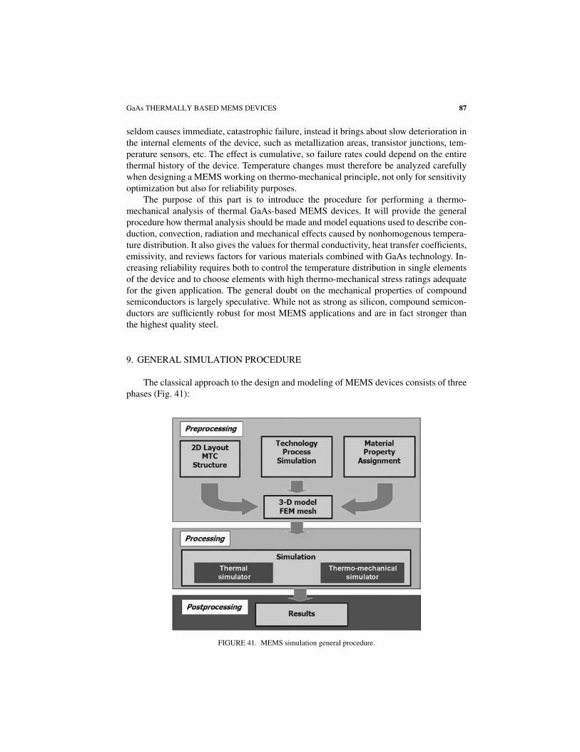
GaAs THERMALLY BASED MEMS DEVICES 87
seldom causes immediate, catastrophic failure, instead it brings about slow deterioration inthe internal elements of the device, such as metallization areas, transistor junctions, tem-perature sensors, etc. The effect is cumulative, so failure rates could depend on the entirethermal history of the device. Temperature changes must therefore be analyzed carefullywhen designing a MEMS working on thermo-mechanical principle, not only for sensitivityoptimization but also for reliability purposes.
The purpose of this part is to introduce the procedure for performing a thermo-mechanical analysis of thermal GaAs-based MEMS devices. It will provide the generalprocedure how thermal analysis should be made and model equations used to describe con-duction, convection, radiation and mechanical effects caused by nonhomogenous tempera-ture distribution. It also gives the values for thermal conductivity, heat transfer coefficients,emissivity, and reviews factors for various materials combined with GaAs technology. In-creasing reliability requires both to control the temperature distribution in single elementsof the device and to choose elements with high thermo-mechanical stress ratings adequatefor the given application. The general doubt on the mechanical properties of compoundsemiconductors is largely speculative. While not as strong as silicon, compound semicon-ductors are sufficiently robust for most MEMS applications and are in fact stronger thanthe highest quality steel.
9. GENERAL SIMULATION PROCEDURE
The classical approach to the design and modeling of MEMS devices consists of threephases (Fig. 41):
FIGURE 41. MEMS simulation general procedure.
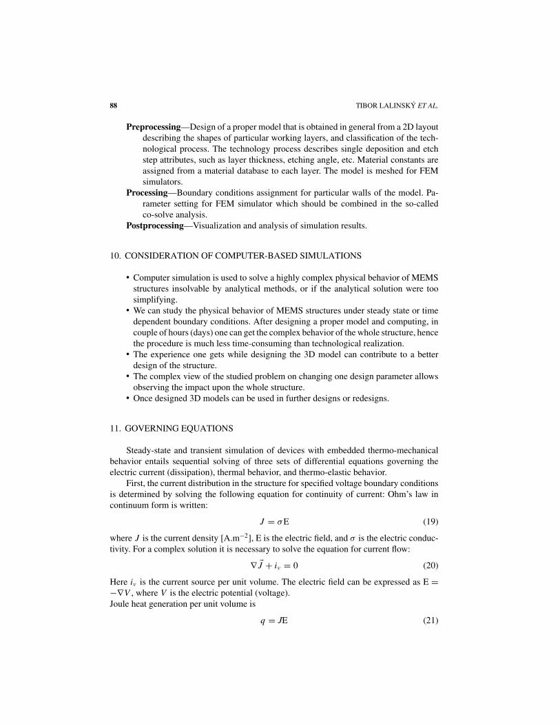
88 TIBOR LALINSKY ET AL.
Preprocessing—Design of a proper model that is obtained in general from a 2D layoutdescribing the shapes of particular working layers, and classification of the tech-nological process. The technology process describes single deposition and etchstep attributes, such as layer thickness, etching angle, etc. Material constants areassigned from a material database to each layer. The model is meshed for FEMsimulators.
Processing—Boundary conditions assignment for particular walls of the model. Pa-rameter setting for FEM simulator which should be combined in the so-calledco-solve analysis.
Postprocessing—Visualization and analysis of simulation results.
10. CONSIDERATION OF COMPUTER-BASED SIMULATIONS
• Computer simulation is used to solve a highly complex physical behavior of MEMSstructures insolvable by analytical methods, or if the analytical solution were toosimplifying.
• We can study the physical behavior of MEMS structures under steady state or timedependent boundary conditions. After designing a proper model and computing, incouple of hours (days) one can get the complex behavior of the whole structure, hencethe procedure is much less time-consuming than technological realization.
• The experience one gets while designing the 3D model can contribute to a betterdesign of the structure.
• The complex view of the studied problem on changing one design parameter allowsobserving the impact upon the whole structure.
• Once designed 3D models can be used in further designs or redesigns.
11. GOVERNING EQUATIONS
Steady-state and transient simulation of devices with embedded thermo-mechanicalbehavior entails sequential solving of three sets of differential equations governing theelectric current (dissipation), thermal behavior, and thermo-elastic behavior.
First, the current distribution in the structure for specified voltage boundary conditionsis determined by solving the following equation for continuity of current: Ohm’s law incontinuum form is written:
J = σE (19)
where J is the current density [A.m−2], E is the electric field, and σ is the electric conduc-tivity. For a complex solution it is necessary to solve the equation for current flow:
∇ �J + iv = 0 (20)
Here iv is the current source per unit volume. The electric field can be expressed as E =−∇V , where V is the electric potential (voltage).Joule heat generation per unit volume is
q = JE (21)
GaAs THERMALLY BASED MEMS DEVICES 89
FIGURE 42. Heat flux definition on solid body.
The steady-state heat conduction equation shown below is solved for specified thermalboundary conditions imposed upon temperature and heat flux (including insulation, naturalconvection, and radiation). The Fourier equation for the distribution of temperature can bewritten as follows:
div(λgradT ) = ρc∂T
∂t− p, (22)
where λ[W m−1K−1] is the coefficient of thermal conductivity, ρ[kg m−3] is the density,c[J kg−1K−1] is the thermal capacity, and p[W m−3] is the specific heat. In the case of largetemperature differences the coefficient of thermal conductivity is not constant, anyhow, inmost MEMS applications it can be taken as constant.
The value of the heat flux can be expressed as:
q = −λgradT [W.m−2], (23)
Fig. 42 shows a solid body placed in coordinates. The heat flux can be expressed as:
q(r, t) = −λ∇T (r, t) (24)
Transcribing the above equation into Cartesian coordinates we get:
qx = −λx∂T (x, y, z, t)
∂x(25)
qy = −λy∂T (x, y, z, t)
∂y(26)
qz = −λz∂T (x, y, z, t)
∂z(27)
For isotropic materials λx = λy = λz . If the solid body is heated up by a constant power andcooled down constantly by the surrounding environment, then the temperature distributionwill settle. For Cartesian coordinates the temperature distribution can be obtained by solvingthe following equation:
∇2T (r, t) + Q(r, t)
λ= 1
α
∂T (r, t)
∂t(28)

90 TIBOR LALINSKY ET AL.
α [m2/s] in equation (28) is the thermal diffusivity and can be expressed as:
α = λ
ρc, (29)
The ambient of thermal MEMS devices are often various gases or liquids. Thus theconvection effects should be also taken into account in some cases (it depends on specificdimensions and shapes of the device; in many cases convection is negligible). Heat transferin gases or liquids has a physical nature different from that in a solid body. Individualparticles can move mutually. The density of heat flux due to convection is given by [91]
q = α′t = α(tst − tt ) [Wm−2], (30)
where α′[W m−2s−1] is the heat transfer coefficient given by the criteria equation (seebelow), tst is the wall temperature of the solid body, tt is the temperature of the surroundinggas or liquid, and A is the contact area. The criteria equation can be found in literature [105]for instance in the following form:
Nu = f (Re,Gr,Pr, . . . .), where (31)
Nu, Re, Gr and Pr are the Nusselt, Reynolds, Grashof and Prandtl numbers, respectively.The criteria equation for natural convection can be expressed in the form:
Nu = C · (Gr.Pr)n, (32)
where C and n depend on the value of the product Gr.Pr according to Tab. 2. For MEMSdevices operating at room temperature the heat loses caused by radiation can be usuallyneglected. On the other hand, radiation can have a significant effect for devices workingmuch above 400 K. Therefore for such devices verification of the radiation effect shouldbe performed. Heat losses caused by radiation are given by the Stefan-Boltzmann emissionlaw:
PRad = ε1,2.C0.AσSB T 4 [W] (33)
where
ε1,2 = 11ε1
+ 1ε2
− 1(34)
ε is the emissivity of gray body, A is the area of the body, and σSB is the Stefan-Boltzmannconstant 5.67 × 10⁻⁸ Wm−2 K−4.
The third and final step in the simulation is to solve the elastic equilibrium equationsunder temperature induced thermal strain. In the linear theory of elasticity, when the de-formation are small the dependence between the strain and stress tensors is given by the
TABLE 2. Value of C and n depends on Gr.Pr
Gr.Pr C n
<1.10−3 0,45 0,0
1.10−3 ∼= 5.102 1,18 0,125
5.102 ∼= 2.107 0,54 0,25
2.107 ∼= 1.1013 0,195 0,333

GaAs THERMALLY BASED MEMS DEVICES 91
FIGURE 43. Mechanical stresses and shear stresses affecting the solid body.
Hook’s law [90]
δx = 1
E
[σx − v
(σy + σz
)](35)
δy = 1
E
[σy − v
(σz + σx
)](36)
δz = 1
E
[σz − v
(σx + σy
)](37)
Here E is the Young’s modulus, σx , σy and σz are the mechanical stresses in mutually orthog-onal directions acting perpendicularly to the wall of the body (Fig. 43), v is the Poisson’sratio. Mechanical structures in the case of the linear theory of elasticity have idealized somephysical properties by the following assumptions: homogeneous body, isotropic, linearlyelastic in all points.
By action of external forces and non-homogeneous temperature distribution, the elasticbody is deformed and internal forces are induced. In a linear elastic continuum, displace-ments appear defined by Lame equation:
(ϕ + ψ) grad (divδ) + ψδ − (3ϕ + 2ψ)αT grad T + f − 0 (38)
where both ϕ ≥ 0 and ψ > 0 are the so-called Lame coefficients given by material param-eters
ϕ = v · E
(1 + v) · (1 − 2v), ψ = E
2(1 + v), (39)
where E(r, T ) [MPa] is the Young’s modulus, ν(r, T ) is the Poisson’s coefficient, δ(r ) [m]
92 TIBOR LALINSKY ET AL.
and f (r, . . .) [Nm−3] are the vector of displacement and the vector of internal volume forces,respectively.
12. BOUNDARY CONDITIONS
Varying thermal and mechanical boundary conditions can significantly affect the anal-ysis results of thermo-mechanical MEMS devices. Mechanical boundary conditions definehow the device is constrained from movement. Mechanical conditions can be consideredfixed for a given MEMS device. Thermal boundary conditions, such as conduction, con-vection, and radiation, on the other hand, depend on the surroundings, packaging, etc. Thatis why careful assessment of thermal boundary conditions is necessary.
Precise thermal analysis that includes the conduction, convection and radiation effectsis needed to properly predict the behavior of thermo-mechanical devices. Not only quanti-tative but also qualitative performance can be changed provided that the thermal boundaryconditions are not modeled correctly. In many cases convection and radiation losses fromthe device could be negligible and heat dissipation is entirely due to the heat lost to thesubstrate. It depends on the shape and dimensions of the device. It can be modeled as aconstant ambient temperature condition at the base of the substrate or on the sidewalls of themodel. Such boundary conditions are known as Dirichlet. The aforementioned assumptionmay not be true when the thermal mass of the substrate is not large enough to preservethe ambient temperature. It could happen when an array of thermo-mechanical devices isused. At that moment a natural boundary condition (Neumann boundary condition) mustbe chosen. After completing the thermal analysis we can get no uniform temperature distri-bution at the substrate. The technology process, environment, and packaging of the MEMSdevice are the factors of appropriate boundary conditions decision. The choice of the typeof boundary conditions could significantly affect the device behavior.
13. 3D MODEL
The micromechanical structures used in thermally based MEMS devices are mostlydesigned as free standing structures. To increase the thermal resistance values, they have tobe designed with the thickness as thin as possible. Moreover, optimization of the microme-chanical structure dimensions, particularly of the aspect ratio between the structure lengththat increases the thermal resistance and structure thickness, has to be carried out to findthe best trade-off between the thermal resistance and acceptable mechanical stress.
The main design criterions, such as high electro-thermal conversion efficiency, linearity,short response time, thermal stability, micromechanical integrity and integration devicesimplicity should be taken into account in the MTC design.
Using the FEM simulation tools, three different models of GaAs MTC have beendesigned. The first model represents two symmetrical cantilever beam structures (350 μmlong and 120 μm wide) fixed by a polyimide layer in a rigid GaAs substrate rim. The rimhas been designed 10 μm thick and 200 μm wide for the purpose of thermal and thermo-mechanical simulations (Fig. 44). These dimensions ensure a sufficient mass for simulatorboundary condition setting while keeping the number of simulation nodes at a reasonable
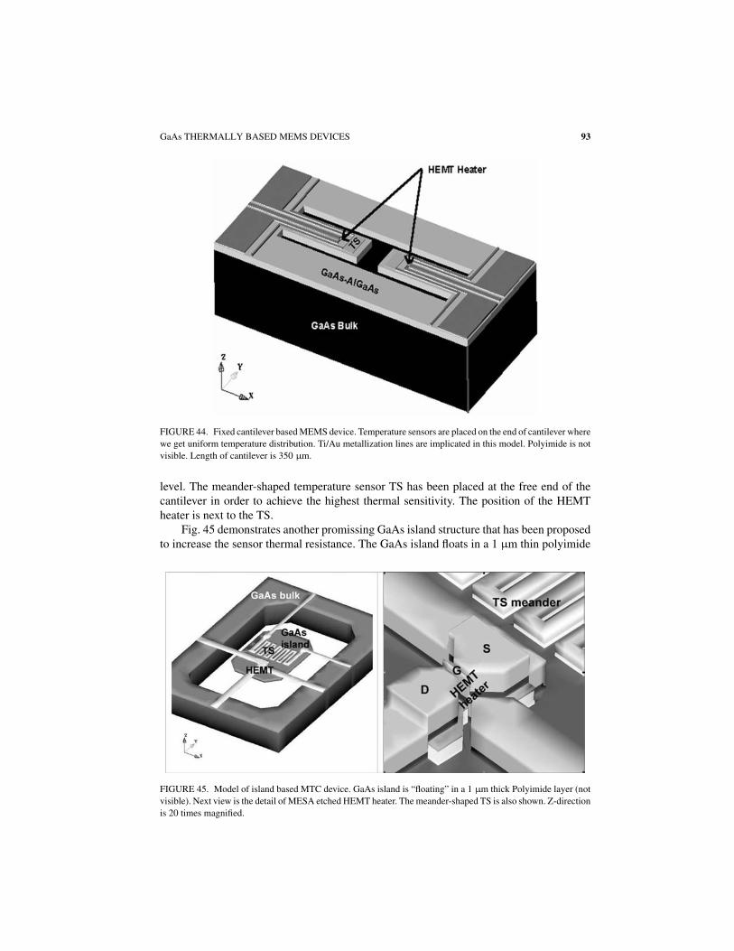
GaAs THERMALLY BASED MEMS DEVICES 93
FIGURE 44. Fixed cantilever based MEMS device. Temperature sensors are placed on the end of cantilever where
we get uniform temperature distribution. Ti/Au metallization lines are implicated in this model. Polyimide is not
visible. Length of cantilever is 350 μm.
level. The meander-shaped temperature sensor TS has been placed at the free end of thecantilever in order to achieve the highest thermal sensitivity. The position of the HEMTheater is next to the TS.
Fig. 45 demonstrates another promissing GaAs island structure that has been proposedto increase the sensor thermal resistance. The GaAs island floats in a 1 μm thin polyimide
FIGURE 45. Model of island based MTC device. GaAs island is “floating” in a 1 μm thick Polyimide layer (not
visible). Next view is the detail of MESA etched HEMT heater. The meander-shaped TS is also shown. Z-direction
is 20 times magnified.
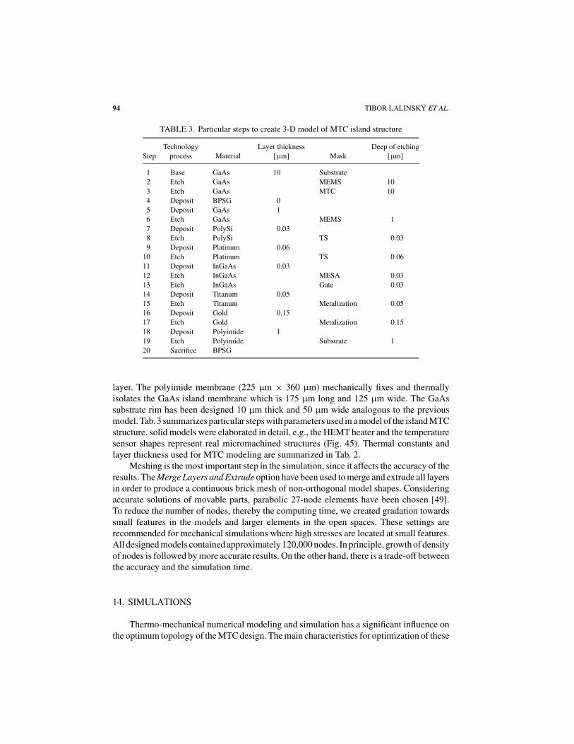
94 TIBOR LALINSKY ET AL.
TABLE 3. Particular steps to create 3-D model of MTC island structure
Technology Layer thickness Deep of etching
Step process Material [μm] Mask [μm]
1 Base GaAs 10 Substrate
2 Etch GaAs MEMS 10
3 Etch GaAs MTC 10
4 Deposit BPSG 0
5 Deposit GaAs 1
6 Etch GaAs MEMS 1
7 Deposit PolySi 0.03
8 Etch PolySi TS 0.03
9 Deposit Platinum 0.06
10 Etch Platinum TS 0.06
11 Deposit InGaAs 0.03
12 Etch InGaAs MESA 0.03
13 Etch InGaAs Gate 0.03
14 Deposit Titanum 0.05
15 Etch Titanum Metalization 0.05
16 Deposit Gold 0.15
17 Etch Gold Metalization 0.15
18 Deposit Polyimide 1
19 Etch Polyimide Substrate 1
20 Sacrifice BPSG
layer. The polyimide membrane (225 μm × 360 μm) mechanically fixes and thermallyisolates the GaAs island membrane which is 175 μm long and 125 μm wide. The GaAssubstrate rim has been designed 10 μm thick and 50 μm wide analogous to the previousmodel. Tab. 3 summarizes particular steps with parameters used in a model of the island MTCstructure. solid models were elaborated in detail, e.g., the HEMT heater and the temperaturesensor shapes represent real micromachined structures (Fig. 45). Thermal constants andlayer thickness used for MTC modeling are summarized in Tab. 2.
Meshing is the most important step in the simulation, since it affects the accuracy of theresults. The Merge Layers and Extrude option have been used to merge and extrude all layersin order to produce a continuous brick mesh of non-orthogonal model shapes. Consideringaccurate solutions of movable parts, parabolic 27-node elements have been chosen [49].To reduce the number of nodes, thereby the computing time, we created gradation towardssmall features in the models and larger elements in the open spaces. These settings arerecommended for mechanical simulations where high stresses are located at small features.All designed models contained approximately 120,000 nodes. In principle, growth of densityof nodes is followed by more accurate results. On the other hand, there is a trade-off betweenthe accuracy and the simulation time.
14. SIMULATIONS
Thermo-mechanical numerical modeling and simulation has a significant influence onthe optimum topology of the MTC design. The main characteristics for optimization of these
GaAs THERMALLY BASED MEMS DEVICES 95
devices are the temperature distribution over the sensing area, the time response, sensitivityand mechanical stresses induced in the multilayer structure.
Three MTC device types have been investigated to compare their thermal and me-chanical behaviour, free standing cantilever, bridge as well as microisland (see above). Thetemperature distribution caused by power dissipation in the heater and the thermal timeresponse as a result of power changes were evaluated by the MemTherm module, andthe mechanical stresses, displacements and deformations were simulated using the thermo-mechanical modules MemMech. The input power dissipation in the heater for the simulationprocess was defined by the heat flux through the HEMT gate area (10 μm × 0.5 μm). Wecan use this approximation because the heat dissipation in HEMT structure is positioned ina very thin InGaAs conduction layer formed under the gate area (see Fig. 12).
15. STEADY STATE THERMAL ANALYSIS AND P-T CHARACTERISTIC
In an isotropic homogeneous material the steady state heat equation can be written as:
∇2T ≡ ∂2T
∂x2+ ∂2T
∂y2+ ∂2T
∂z2= −1
kQ(x, y, z) (40)
where Q represents the generated internal heat, k denotes the thermal conductivity, cp isthe specific heat, and T is the temperature.
In order to complete the specification of the thermal simulations, it is necessary tospecify the boundary conditions. For the thermal analysis problem, the essential boundaryconditions are prescribed by temperatures. Furthermore, the conductive heat flux and theradiation boundary conditions may also be applied. The spatial temperature distribution ofthe MTCs and steady state heat flux were calculated taking into account the heat transfersto infinity. In the current analysis, according to application requirements, the fixed thermalboundary is defined for all sidewalls of the GaAs substrate. These sides were kept at roomtemperature of 300 K while other sides were adiabatic. The CoventorWare simulationmanager (SimMan) was used to investigate the influence of power dissipation in the heater.
Plots give a good overall visualization of the temperature distribution (Fig. 46) in theisland MTC structure. Shading and z-direction value represent the temperature distributionfor 1 mW power dissipation from the HEMT heater. The island is “floating” in the polyimidelayer that mechanically and thermally isolates the MTC structure. The polyimide layer isnot shown but was considered in the simulation. Analyses were performed for both vacuumambient and non-convective gaseous medium around the MTC structure. Heat losses dueto radiation were taken into account too, in the simulation but were found to be negligible.Thermal material properties choised are summarized in Tab. 4.
The power-to-temperature (P-T ) conversion characteristics of the MTC structureshave been investigated and they were also compared with that of real micro-machineddevices. Figure 47 shows the simulated P-T conversion characteristics of an island-basedMTC device in direct comparison with both the fixed cantilever and bridge based MTCcomponents. The slope of the P-T curves determines the thermal resistance values, Rth.The benefit from the improved electro-thermal conversion efficiency of the island structureis clearly visible. Thermal resistance as high as 24 K/mW has been achieved, which is

96 TIBOR LALINSKY ET AL.
TABLE 4. Selected thermal material properties
Thickness of
deposited Thermal expansion Thermal conductivity Specific heat
Material layer [μm] coefficient [m.K−1] [W.m−1K−1] [J.kg−1.K−1] Mark
SI-GaAs 10 6.8∗10−6 46 351 Substrate
GaAs 1 6.8∗10−6 46 351 MTC layer
PolySi 0.03 4.7∗10−6 148 107 Temperature Sens.
Platinum 0.06 8.9∗10−6 71.6 133 Temperature Sens.
GaAs 0.02 6.8∗10−6 46 351 HEMT heater
Titanum 0.05 1.0∗10−5 21.9 528 Metalization
Gold 0.15 1.41∗10−5 267 129 Metalization
Polyimide 1 6.0∗10−6 1.46∗10−1 510 Mech. Fixing
FIGURE 46. 3-D plots of temperature distribution of island based MTC device. The island is “floating” in
polyimide layer that mechanically and thermally isolates the MTC structure. Polyimide not shown.
FIGURE 47. Simulated island, cantilever and bridge P-T conversion characteristics. Comparison with real mi-
cromachined MTC device. Ambient temperature for bridge MTC was 285 K whereas other two MTCs ambient
temperatures were 300 K.
GaAs THERMALLY BASED MEMS DEVICES 97
FIGURE 48. The simulated power on/off transient characteristics for island MTC structure for power ON of
1 mW. At the beginning there was power of 1 mW switched ON. In the time of 4 ms the power was switched OFF.
two-times higher than that of the bridge-based MTC element (11.5 K/mW). When comparedwith experiment, the thermal resistance values are congruent.
16. TEMPERATURE TRANSIENT ANALYSIS
The transient thermal response characteristics evaluation of the MTC structures mostlycan be regarded as essential. Instantaneous temperature distribution on the body of MTCcan be obtained solving the thermal transient equation:
∂T
∂t= k
ρcp∇2T (41)
where ρ denotes the density of the material and k its thermal conductivity. Thermal bound-ary conditions has been applied the same as for steady-state analysis. Additionally, thetemperature of the MTC body was defined at time t = 0 to be 300 K.
Simulated transient on/off power characteristics for an island structure are depictedin Fig. 48. At the beginning a power of 1 mW was switched ON. After 4 ms the powerwas switched OFF. The thermal time constant obtained as 1.5 ms. There are two transientsin Fig. 48. The upper one is the temperature of the heater and the bottom dependenceshows the average temperature of the TS. The thermal time constant of the cantilever beamarrangement is 1.7 ms, which is nearly consistent with that of the island MTC structure.
17. STRESS AND DISPLACEMENT EVALUATION
As was noted above, mechanical stresses can have a great influence on the mechanical aswell as electrical properties. The initial residual stresses caused by temperature differencesduring membrane layers deposition were evaluated analytically and experimentally [87].
98 TIBOR LALINSKY ET AL.
FIGURE 49. Displacement magnitude (in μm) along the length of the bridge in Z direction caused by initial
stress in metallization. Comparison between bridge fixed by polyimide layer and bridge where polyimide layer
was removed is shown. A cross section was made in the middle of the bridge in X-axes direction.
Analytical calculation has been performed using a simple analytical expression (12).The initial stress in the metallization (before bridge etching) for temperature differenceT = 170 K was calculated 81.6 MPa for Ti and 51.3 MPa for Au layer, respectively.Thus, after the etching of GaAs substrate base, the mean stress throughout the thicknessof membrane bridge structure is about 25 MPa. The experimental measurement by thedetection of the membrane deflection amplitudes as a response to acoustic pressure givesthe value of the mean membrane stress aproximately 21.6 MPa (see above). As seen, theresult is consistent well with the simple analytical calculation [19].
Figure 49 shows the displacement magnitude in z-axis direction along the length of thebridge caused by initial stress in Au/Ti metallization. Comparison is shown between thebridge fixed by a polyimide layer and the bridge where the polyimide layer was removed.A cross section was drawn in the middle of the beam in x-axis direction. As it can be seenthe polyimid film reduces strongly the deformation of this mechanical component.
In order to model MTC devices, the combination of the heat conduction equationswith the linear elasticity has to be done. Mechanical and thermal boundary conditions weredefined for the sidewalls of the GaAs substrate. These sides were kept at room temperature300 K while other sides were adiabatic and were set as rigid, i.e., immobile. The initialstress was set in each material according to the analytical calculation.
The stress and displacement magnitude were simulated using MemMech simulator.The mechanical material properties are summarized in Tab. 5. Figure 50 shows the plotof residual stresses and the deformation of the island structure caused by heating. Shad-ing represents the residual stress for 1 mW power dissipation in the heater. The biggeststresses (520 MPa) are located in the place of the meander-shaped PolySi temperature
GaAs THERMALLY BASED MEMS DEVICES 99
TABLE 5. Selected mechanical material properties
Poisson Mechanical
Young modulus coefficient Density stress
Material [GPa] [−] [kg.m−3] [MPa] Mark
SI-GaAs 85 0.31 5370 — Substrate
GaAs 85 0.31 5370 — MTC layer
PolySi 160 0.22 2230 — Temperature Sensor
Platinum 145 0.35 21 400 — Temperature Sensor
GaAs 85 0.31 5370 — HEMT heater
Titanum 120 0.33 4506 81.61 Metalization
Gold 78 0.29 19 300 51.342 Metalization
Polyimide 2.4 0.3 1100 — Mechanical fixation
sensor. The MTC structure is fixed by a polyimide layer that is not shown in the figurebut was taken into account during simulation. The scale magnification in z-direction is10× and the displacement magnification is 2×. The maximum stress has been located inSi/Pt meander-shaped TS. For power dissipation of 3 mW, the TS temperature is 375 Kand the mechanical stress reaches up to 900 MPa. These values of residual MTC stresses,however, have no significant influence upon the micromechanical integrity of the MEMSdevice.
FIGURE 50. Residual stresses and deformation of the island structure caused by heating up with power dissi-
pation of 1mW in the heater. Polyimide layer was investigated in simulation (not visible). Values of stress are in
MPa.
100 TIBOR LALINSKY ET AL.
TABLE 6. Comparison of the designed island based MTC devices (Island structure
suspended with and without GaAs bridge)
Island without Island with Optimized island
GaAs GaAs with GaAs
Rth simulation [K/mW] 24 13 26
Rth measurement [K/mW] — 14 —
τ simulation [ms] 0.9 0.9 0.8
τ measurement [ms] — 0.8 —
Max. temperature [K] (1 mW) 332 320 336
Max. displacement [μm] [1 mW] 2.74 0.26 5.28
Max. mechanical stress [Mpa] (1 mW) 540 434 284
18. INFLUENCE OF THE GATE WIDTH ON MAXIMAL TEMPERATUREOF MTC STRUCTURE
The influence of the gate width on the maximum temperature of MTC structure has beensimulated. Temperature distributions in the HEMT and in the MTC structure for differentgate widths (5 μm, 10 μm, 15 μm, 20 μm) have been obtained. From the simulation resultsit follows that the maximum temperature of the MTC microstructure which is located inthe gate of the HEMT is inversely proportional to the gate width (see Fig. 51 and Fig. 52).
FIGURE 51. Temperature distribution in the HEMT and in the MTC structure for different gate widths: (a) 5 μm,
(b) 10 μm, (c) 15 μm, (d) 20 μm. Dissipated power in the HEMT was 0.5 mW. From the simulation results follows
that the temperature of the MTC structure remains the same.

GaAs THERMALLY BASED MEMS DEVICES 101
FIGURE 52. Maximal and average temperature—HEMT gate width dependence. Dissipated power in the HEMT
was 0.5 mW.
It has been also approved that the temperature sensed by the temperature sensor remainedthe same. It can be concluded that the HEMT gate width has no influence on the resultingsensitivity, only the maximum temperature changes. In order to minimize the maximumtemperature of the sensor it is desirable to increase the HEMT gate width as soon as possible.The dissipated power is then generated in a greater volume. Due to the reduction of themaximum temperature the sensor structure could be used for a wider field of measuredpower while the sensitivity remains the same.
19. OPTIMIZATION OF THE DESIGN
The design criteria to assess the general performance and considerations of the sensorare given below:
• Reduced maximum stress in both the GaAs substrate and the Ti/Au metallizationlayers, particularly in the heated active area of the MTC device.
• Uniform temperature distribution over the sensing element (meander-like temperaturesensor).
• Increased sensitivity (dissipated power-to-temperature conversion).• Quick time response (change of temperature as a result of changed input power).
According to the above criteria, extensive models of the MTC structure have been designedand numerical simulations have been carried out to evaluate the performance of the sensor.
102 TIBOR LALINSKY ET AL.
FIGURE 53. 3-D model of the optimized island based MTC device. The scale factor in the z direction was
multiplied by 10. The polyimide layer is not shown. On the right figure the detail of HEMT and temperature sensor
is shown.
A new optimized island structure design reduces the maximal stress caused by tem-perature changes, minimizes the heat losses caused by too short supplying metallization tothe HEMT transistor. The model is depicted in Fig. 53. The gate supplying metallizationwas led around the island so as to lengthen it as much as possible. Temperature losses areminimized by this solution. Another advantage of such a topology is that all metallizationsenter the substrate surface in the same location and there is no other metallization on theopposite site. Mechanical compressions are minimized by this solution, as well.
A steady state temperature analysis has been performed to propose the sensitivity andthermal resistance of the structure. The temperature distribution caused by power dissipationin the heater and the thermal time response as a result of power changes were evaluated by theMemTherm module. For simulation, the input power dissipation in the heater was definedby the heat flux through the HEMT gate area (10 μm × 0.5 μm). We can use this approxi-mation because heat dissipation in the HEMT structure takes place in a very thin conductivelayer formed under the gate area. For the thermal analysis problem, the essential boundaryconditions are prescribed temperatures. Furthermore, the conductive heat flux and radiationboundary conditions may also be applied. The spatial temperature distribution of the MTCsand steady state heat flux were calculated taking into account the heat transfers to infinity. Inthe current analysis, according to the application requirement, the fixed thermal boundary isdefined for all sidewalls of the GaAs substrate. These sides were kept at room temperature300 K while other sides were adiabatic. The CoventorWare simulation manager (SimMan)was used to investigate the influence of the power dissipation in the heater. Plots give agood overall visualization of temperature distribution (Fig. 54) in the island MTC structure.The island is “floating” in the polyimide layer that mechanically and thermally isolates theMTC structure. The polyimide layer is not shown but was considered in the simulation.
The analyses have been performed for both vacuum ambient and non-convectivegaseous medium around the MTC structure. The heat losses due to radiation were taken into
GaAs THERMALLY BASED MEMS DEVICES 103
FIGURE 54. 3-D plots of temperature distribution of the island based MTC device. The island is “floating” in
polyimide layer that mechanically and thermally isolates MTC structure. Polyimide not shown. The scale factor
in the z direction was multiplied by 10.
account in the simulation but were found to be negligible. The thermal boundary conditionwas set the same as for the steady-state analysis. Additionally, the temperature of the MTCbody was defined at time t = 0 to be 300 K. Simulated transient on/off power characteristicsfor the island structure are depicted in Fig. 55. At the beginning, a power of 1 mW wasswitched ON. After 5 ms the power was switched OFF. The thermal time constant of theisland structure arrangement is 0.8 ms. Both, mechanical and thermal boundary conditions
FIGURE 55. The simulated power on/off transient characteristics for island based MTC device for power ON of
1 mW. At the beginning there was power of 1 mW switched ON. In the time of 5 ms the power was switched OFF.
104 TIBOR LALINSKY ET AL.
FIGURE 56. Residual stresses and deformation of the island structure caused by heating up with power dissipation
of 1mW in the heater Left fig.: island structure, Right fig.: optimised island structure, Polyimide layer was
investigated in simulation (not visible). Values of stress are in MPa.
were defined for the sidewalls of the GaAs substrate. These sides were kept at room tem-perature 300 K while other sides were adiabatic and were set as rigid, i.e., immobile. Theinitial stress was set in each material according to analytical calculation.
The stress and displacement magnitude were simulated using MemMech simulator.Figure 56 shows the plot of residual stresses and a deformation of the island structure andof the optimized island structure caused by heating. Shading represents the residual stressfor 1 mW power dissipation in the heater. The higher stresses (616 MPa) are located in theplace of the meander-shaped PolySi temperature sensor. As seen, the stress is significantlyreduced in the optimized island structure design (284 MPa). The scale magnification inz-direction is 10× and the displacement magnification is 2×.
20. ACKNOWLEDGEMENTS
This work was supported, in part, by the NATO SfP Project No.: SfP-974172, CECCOPERNICUS programme—contract No.: CIPA-CT94-0197, Slovak Government con-tract (No.: 2003 SO 51/03 R06 00/03R06 02-2003), and by the Science and Technol-ogy Assistance Agency under the contract No.: APVT-51-032902. The authors wouldlike to thank to Prof. Z. Hatzopoulos from University of Crete for MBE growth of theAlGaAs/InGaAs/GaAs based heterostructures. The authors wish also to thank to researchteam of the Department of Microelectronics Structures of the Institute of Electrical Engi-neering, SAS, Bratislava (first of all to S. Hascık, Z. Mozolova, M. Grujbar, and I. Benkovic)for participation in the sophisticated MEMS device processing technology. The thanks be-longs also to all colleagues from the Department of Electron Beam Lithography of theInstitute of Informatics, SAS, Bratislava, for assistance in the device processing technologyand fabrication of the required sets of lithographic masks.
GaAs THERMALLY BASED MEMS DEVICES 105
REFERENCES
1. Leclercq, J.L., Ribas, R.P., Karam J.M., and Viktorovitch P., III–V Micromachined Devices for Microsystems,
Microelectronics Journal, 1998;29:613–619.
2. Hjort, K., Soderkvist J., and Jan-Ake Schweitz, Galium Arsenide as a Mechanical Material, J. Micromech.Microeng., 1994;4:1–13.
3. Lalinsky, T., Kuzmık, J., Porges, M., Hascık, S., Mozolova, Z., and Grno L., Monolithic GaAs MESFET
Power Sensor Microsystem, Electronics Letters, 1995;31:1914–1915.
4. Soderkvist J., A phenomenological Method of Predicting the Performance of Piezoelectric Beams, J. Mi-cromech. Microeng., 1991;1:16–24.
5. Ho, F. and Yamamoto, Y., Piezoresistive-piezoelectric Gallium Arsenide Atomic Force Microscope Can-
tilever, ERATO Quantum Fluctuation Project, E.L. Ginzton Laboratory, Stanford University, http://www-
snf.stanford.edu
6. Hascık, S., Lalinsky, T., Kuzmık, J., Porges, M., and Mozolova, Z., The fabrication of Thin GaAs Cantilever
Beams for Power Sensor Microsystem Using RIE, Vacuum, 1996;47:1215–1217.
7. Hascık, S., Lalinsky, T., Mozolova Z., and Kuzmık, J., Patterning of Cantilevers for Power Sensor Microsys-
tem, Vacuum, 1998;51:307–309.
8. Karam, J.M., Courtois, B., Holio, M., Leclercq, J.L., and Viktorovitch, P., Collective Fabrication of Gallium
Arsenide Based Microsystems, Proceeding SPIE-micromachining and Microfabrication Process Tech. II,1996, Vol. 2879, pp. 315–326.
9. Ribas, R.P., Leclercq, J.L., Karam, J.M., Courtois, B., and Viktorovitch, P., Bulk Micromachining Character-
ization of 0.2 μm HEMT MMIC Technology for GaAs MEMS Design, Materials Science and Engineering,
1998;B51:267–273.
10. Fobelets, K., Vounckx R., and Borghs, G., A GaAs Pressure Sensor Based on Resonant Tunneling Diodes,
J. Micromech. Microeng., 1994;4:123–128.
11. Dehe, A., Fricke, K., Mutanba K., and Hartnagel, H.L., A Piezoresistive GaAs Pressure Sensor with
GaAs/AlGaAs Membrane Technology, J. Micromech. Microeng., 1995;5:139–142.
12. Lalinsky, T., Burian, E., Mozolova, Z., Hascık, s., Kuzmık, J., Bohacek, P., and Hatzopoulos, Z., The
improvment in GaAs Power Sensor Microsystem Technology and Simulation, MICROSIM II—Simulationand Design of Microsystems and Microstructures, in R.A. Adey and Ph. Renaud (Ed.), Computational
Mechanics Publications, Southampton, UK, Boston, USA, 1997, pp. 43–51.
13. Lalinsky, T., Hascık, S., Mozolova, Z., Kuzmık, J., and Hatzopoulos, Z., Power Sensor Microsystem Tech-
nology and Characterization, Sensor and Materials, 1998;10:241–250.
14. Lalinsky, T., Hascık, S., Mozolova, Z., Burian, E., and Drzık, M., The Improved Performance of GaAs
Micromachined Power Sensor Microsystem, Sensors Actuators A, 1999;76:241–246.
15. Dehe, A., Krozer, V., Fricke, K., Klingbeil, H., Beilenhoff, K., and Hartnagel, H.L., Integrated Microwave
Power Sensor, Electronics Letters, 1995;31:2187–2188.
16. Dehe, A., Krozer, V., Chen B., and Hartnagel, H.L., High-sensitivity Microwave Power Sensor for GaAs-
MMIC Implemention, Electronics Letters, 1996;32:2149–2150.
17. Salzenstein, P., Dupois, O., Helal, M., Lheurette, E., Vanbesien, O., Mounaix, P., and Lippens, D., Coplanar
Waveguides on Dielectric Membranes Micromachined on a GaAs Substrate, Electronics Letters, 1996;32:
821–822.
18. Dehe, A., Fricke, K., and Hartnagel, H.L., Infrared Thermopile Sensor Based on AlGaAs-GaAs Microma-
chining, Sens. Actuators A, 1995;46–47:432–436.
19. Lalinsky, T., Drzık, M., Tomaska, M., Krnac, M., Hascık, S., Mozolova, Z., Klasovity, M., and Kostic,
I., Coplanar Waveguides Supported by InGaP and GaAs/AlGaAs Membrane-like Bridges, J. Micromech.Microeng., 2002;12:465–469.
20. Heisig, S. and Oesterschulze, E., Gallium Arsenide Probes for Scanning Near-field Probe Microscopy, Appl.Phys., 1998;A66:S385–S390.
21. Iwata, N., Wakayama, T., and Yamada, S., Establishment of Basic Process to Fabricate full GaAs Cantilever
for Scanning Probe Microscope Applications, Sensors and Actuators A, 2004;111;26–31.
22. Lalinsky, T., Hascık, S., Mozolova, Z., Drzık, M., and Hatzopoulos, Z., Micromachined Power Sen-
sor Microsystem, Micromechanics Europe Workshop, Ulvik in Hardanger, Norway, 1998, pp. 139–
142.

106 TIBOR LALINSKY ET AL.
23. Lalinsky, T., Drzık, M., Hascık, S., Mozolova, Z., Kuzmık J., and Hatzopoulos, Z., Study of Bimetallic
Effect in a GaAs Cantilever Beam of Power Sensor Microsystem, 2nd International Conference on AdvancedSemiconductor Devices and Microsystems, Smolenice Castle, Slovakia, 1998, pp. 331–334.
24. Johansson, S., Ericson, F., and Jan-Ake Schweitz, Influence of Surface Coatings on Elasticity, Residual
Stress, and Fracture Properties of Silicon Microelements, J. Appl. Phys., 1989;65:122–128.
25. Lalinsky, T., Burian, E., Drzık, M., Hascık, S., Mozolova, Z., and Kuzmık, J., Thermal Actuation of a GaAs
Cantilever Beam, J. Micromech. Microeng., 2000;10:293–298.
26. Lalinsky, T., Burian, E., Drzık, M., Hascık, S., Mozolova, Z., Kuzmık, J., and Hatzopoulos, Z., Performance
of GaAs Micromachined Microactuator, Sensors and Actuators, 2000;85:365–370.
27. Brice, J.C., Properties of Gallium Arsenide, 2nd Edition, EMIS Datareviews Series No. 2 (INSPEC (IEE),
London, 1990), p. 7.
28. Takahashi, N.S., Properties of Aluminium Gallium Arsenide, in S. Adachi (Ed.), EMIS Datareviews SeriesNo. 7, (INSPEC (IEE), London, 1993), p. 3.
29. Adachi, S., GaAs and Related Materials (Bulk Semiconducting and Superlattice Properties), ISBN9810219253, World Scientific Publishing Co. Pte. Ltd, 1994.
30. Adachi, S., Lattice Thermal Resistivity of III–V Compound Alloys, J. Appl. Phys. 1983;54:1844–1848.
31. Adachi, S., GaAs, AlAs and AlxGa1−xAs Material Parameters for Use in Research and Device Applications,
J. Appl. Phys. 1985;58:R1-29.
32. Walkey, D.J., Smy, T.J., Macelwee, T., and Maliepaarad, M., Compact Representation of Temperature and
Power Dependence of Thermal Resistance in Si, InP and GaAs Substrate Devices Using Linear Models,
Solid-State Electronics, 2002;46:819–826.
33. Hjort, K., Sacrificial Etching of III–V Compounds for Micromechanical Devices J. Micromech. Microeng.,1996;6:370–375.
34. Collins, S.D., Etch Stop Techniques for Micromachining, J. Electrochemical Society, 1997;144:2242–2262.
35. Fricke, K., Wurf, J., Miao, J., Dehe, A., Ruck, D., and Hartnagel, H.L., Fabrication of Microstructures for
Integrated Sensors on GaAs, J. Micromech. Microeng., 1993;3:131–134.
36. Miao, J., Hartnagel, H.L., Ruck, D., and Fricke, K., The Use of Ion Implantation for Micromachining GaAs
for Sensor Application, Sensors and Actuators A, 1995;46–47:30–34.
37. Uenishi, Y., Tanaka, H., and Ukita, H., Characterization of AlGaAs Microstructure Fabricated by
AlGaAs/GaAs Micromachining, IEEE Trans. On Electron Devices, 1994;41:1778–1783.
38. Chong, N., Srinivas, T.A.S., and Ahmed, H., Performance of GaAs Microbridge Thermocouple Infrared
Detectors, Journal of Microelectromechanical Systems, 1997;6:136–141.
39. Ribas, R.P., Maskless Front-Side Bulk Micromachining Compatible to Standard GaAs IC Technology, Thesis,
TIMA-CMP, Grenoble Cedex, France.
40. TIMA-Circuits Multi-Projects (CMP) Laboratory: 0.2 μm pHEMT GaAs E/D from OMMIC, Compatible
Front-side Bulk Micromachining, Grenoble Cedex, France.
41. Lalinsky, T., Drzık, M., Matay, L., Kostic, I., Mozolova, Z., Hascık, S., and Krajcer, A., InGaP/Polyimide
Membrane-like Bridges Fully Compatible with InGaP/InGaAs/GaAs Based HFETs, Proceedings of theInternational MEMS Workshop—iMEMS, Singapore, July 4–6, 2001, pp. 362–368, to be Published Also in
Materials & Process Integration for MEMS, Edited by Francis E.H. Tay, Singapore, ISBN 1-4020-7175-2,
2002, pp. 53–75.
42. Lalinsky, T., Hascık, S., Mozolova, Z., Burian, E., Tomaska, M., Krnac, M., Drzık, M., Skriniarova, J.,
Kostic, I., and Matay, L., Mechanically Fixed and Thermally Isolated Micromechanical Structures for GaAs
Heterostructure Based MEMS Devices, Proceedings of the International Symposium on Microelectronics,
Colorado, September 4–6 2002, pp. 87–92—to be Published Also in Microelectronics International, January
20, 2003, pp. 43–47.
43. Lalinsky, T., Hotovy, I., Hascık, S., Mozolova, Z., Kuzmık, J., and Pogany, D., Thin Film Resistance
Temperature Sensors on GaAs, Proceeding of ASDAM’ 98 Conference, Smolenice Castle, Slovakia, 1998,
pp. 243–246.
44. Lalinsky, T., Hrkut, P., Mozolova, Z., Kovacik, T., and Krajcer, A., Thermal Performance and Stability of
Poly Si/Pt(Ni) Thin Film Temperature Sensors on GaAs, Proceedings of the 11th International Conferenceon Solid-State Sensors and Actuators, Munich, June 10–14, 2001, pp. 1496–1499.
45. Fricke, K., Hartnagel, H.L., Ritter, S., and Wurfl, J., Micromechanically Structurized Sensors on GaAs: an
Integrated Anemometer, Microelectronics Engineering, 1992;19:195–198.
GaAs THERMALLY BASED MEMS DEVICES 107
46. Fricke, K., A Micromachined Mass-flow Sensor With Integrated Electronics on GaAs, Sensors and ActuatorsA, 1994;45:91–94.
47. Dehe, A. and Hartnagel, H.L., Free-standing AlGaAs Thermopilesfor Improved Infrared Sensor Design,
IEEE Trans. on Electron Devices, 1996;43:1193–1199.
48. Hava, S. and Hunsperger, R., Thermoelectric Properties of AlxGa1−xAs, J. of Appl. Phys., 1985;57:5330–
5335.
49. Pogany, D., Seliger, N., Lalinsky, T., Kuzmık, J., Habas, P., Hrkut, P., and Gornik, E., Study of Thermal
Effects in GaAs Micromachined Power Sensor Microsystems by An Optical Interferometer Technique,
Microelectronics Journal, 1998;29:191–198.
50. Burian, E., Pogany, D., Lalinsky, T., Seliger, N., and Gornik, E., Thermal Simulation and Characterization
of GaAs Micromachined Power Sensor Microsystems, Sensors Actuators A, 1998;68:372–377.
51. Lalinsky, T., Hascık, S., Mozolova, Z., Drzık, M., and Hatzopoulos, Z., The Improved Performance of GaAs
Micromachined Power Sensor Microsystem, Proceedings of the 12th European Conference on Solid-StateTransducers-EUROSENSORS XII, Southampton, September 13–16, 1998, pp. 739–742.
52. Dehe, A., Peerlings, J., Pfeiffer, J., Riemenschneider, R., Vogt, A., Streubel, K., Kunzel, H., Meissner, P., and
Hartnagel, H.L., III–V Compound Semiconductor Micromachined Actuator for Long Resonator Tunable
Fabry-Perot Detector, Sensors and Actuators A, 1998;68:365–371.
53. Lalinsky, T., Krnac, M., Drzık, M., Hascık, S., and Mozolova, Z., Micromechanical Thermal Converter
Device Based on Polyimide-fixed Island Structure, The 14th Micromechanics Europe Workshop-MME03,
Delft, November 2–4, 2003, pp. 45–48.
54. Lalinsky, T., Drzık, M., Chlpık, J., Krnac, M., Hascık, S., and Mozolova, Z., Thermo-Mechanical Char-
acterization of Micromachined GaAs Based Thermal Converter Using Contactless Optical Methods, In:
Proceedings of EUROSENSORS XIII Conference, Roma September 12–15, 2004, p. 239.
55. Microwave Monolithic Integrated Transmitted Power Sensors and Their Industrial and Metrological Appli-
cations, NATO SfP project No.: SfP-974172.
56. Born, M. and Wolf, E., Principles of Optics, Pergamon Press, New York, 1975.
57. Ohring, M., The Material Science of Thin Films, Academic Press, New York, 1992.
58. Bertollotti, M., Bogdanov, V., Ferrari, A., Jascow, A., Nazarova, N., Pikhtin, A., and Schirone, L., Temperature
Dependence of the Refractive Index in Semiconductors, J.Optical Soc. of America, 1990;7:918–922.
59. McCaulley, J.A., Donnelly, V.M., Vernon, M., and Taha, I. Temperature Dependence of the Near-infrared
Refractive Index of Silicon, Gallium Arsenide, and Indium Phosphide, Physical Review B, 1994;49:7408–
7017.
60. Tiziani, H.J., Optical Metrology of Engineering Surfaces—Scope and Trends, in P.K. Rastogi (Ed.), OpticalMeasurement Techniques and Applications, Artech House, Boston, 1997, pp. 15–49.
61. Sheppard, C.J.R. and Roy, M., Low-coherence Interference Microscopy, in P. Torok and F.-J. Kao (Eds.),
Optical Imaging and Microscopy, Springer, Berlin, 2003.
62. Davis, C.Q. and Freeman, D.M., Using a Light Microscope to Measure Motions with Nanometer Accuracy,
Optical Engineering, 1998;37:1299–304.
63. Sheppard, C.J.R., Roy, M., and Sharma, M.D., Image Formation in Low-coherence and Confocal Interference
Microscopes, Applied Optics, 2004;43:1491–1502.
64. Bosseboef, A. and Petitgrand, S., Characterization of the Static and Dynamic Behaviour of M(O)EMS by
Optical Techniques: Status and Trends, Proceeding MME‘02, Sinaia, Romania, 2002, pp. 229–241.
65. Wilson, T., Confocal Microscopy, Academic Press, New York, 1990.
66. PLμ: Confocal Imaging Profiler, The Innovative Concept for Non-contact 3D, http://www.atos-online.de.
67. Jordan, H.J., Brodmann, R., Valentin, J., and Grigat, M., Confocal White Light Microscopy, http://www.
nanofocus-inc.com/html.
68. Vlassak, J.J. and Nix, W.D., A New Bulge Test Technique for The Determination of Young’s Modulus and
Poisson’s Ratio of Thin Films, J. Mater. Res., 1992;7:3242–3249.
69. FLATSCAN 200—Automated 2D/3D—Measurement System for Thin Film Stress and Surface Curvature,
http://www.oeg-messtechnik.de.
70. KLA Tencor FLX-2320-S Film Stress Measurement System, http://www.lot-oriel.com/pdf/all/kla
filmstress.pdf.
71. Drzik, M., Vanek, O., and Kempny, M., Silicon Wafers Deformation Measurement by Using Optical Methods,
Proceeding of 41st International Science Colloquium, 1996, Vol. 1, pp. 597–602.
108 TIBOR LALINSKY ET AL.
72. Nemcsics, A., Szabo, J., Gurban, S., and Csontos, L., Mechanical Study of the Strained InxGa1−xAs/GaAs
Heterostructures, in J. Novak and A. Schlachetzki (Eds.), Heterostructure Epitaxy and Devices, Kluwer
Academic Publ., 1996, pp. 103–106.
73. Drzik, M., Butschke, J., Fallmann, W., Haugeneder, E., and Loeschner, H., Optical Measurement of Stress
in Thin Membranes, Proceeding of 26th IMEKO World Congress, Vienna, CD-ROM, 2000.
74. Levtchenko,V.M. and Gulidov, D.N., Mechanical Treatment of Semiinsulator (SI) GaAs (100) and its Ef-
fect on Geometrical and Electro-physical Parameters, Proceeding of 5th Science and Business ConferenceSILICON‘96 Vol. 2 Roznov p. Radhostem, 1996, pp. 278–292.
75. Gunnars, J. and Wiklund, U., Determination of Growth-induced Strain and Thermoelastic Properties of
Coatings by Curvature Measurements, Materials Science and Engineering, 2002; Vol. A336, pp. 7–21.
76. Chen, K.-S. and Ou, K.-S., Modification of Curvature-based Thin-film Residual Stress Measurement for
MEMS Applications, J. Micromech. Microeng., 2002;12:917–924.
77. Fang, W. and Wickert, J.A., Comments on Measuring Thin-film Stresses Using Bi-layer Micromachined
Beams, J. Micromech. Microeng., 1995;5:276–281.
78. Yang, J.C.S., Prevention of Thermal Bending of Multilayered Beams and Plates, Experimental Mechanics1975;15:418–423.
79. Suhir, E., Stresses in Bi-metal Thermostats, J. Applied Mechanics, 1986;53:657–660.
80. Lavitska, E., Thermal Strain and Its Influence on Characterization of Semiconductor Elements, Pro-ceeding of 5th NEXUSPAN Workshop on Thermal Aspects in Microsystem Technology, Budapest, 1998;
pp. 115–120.
81. Zhang, X., Ghodssi, R., Chen, K.-S., Ayon, A.A., and Spearing, S.M., Residual Stress Characterization of
Thick PECVD TEOS Film For Power MEMS Applications, Proceeding of Solid- State Sensor and ActuatorWorkshop, Hilton Head Is, SC, 2000, pp. 1–4.
82. Castellini, P., Revel, G.M., and Scalise, L., Application of Lasers for Non-contact Excitation and Measurement
of Vibration, Proceeding SPIE—4th Int. Conference on Vibration Measurements by Laser Technique, 2000,
Vol. 4072, pp. 280–291.
83. Jia, W. and Enyao, Zh., Applications of Laser Vibrometer in Vibration Measurement of Microstructures,
Proceeding SPIE, 1996;2868:318–325.
84. Petitgrand, S., Yahiaoui, R., Bosseboef, A., and Danaie, K., Quantitative Time-average Microscopic Inter-
ferometry for Micromechanical and Art Conservation, Proceeding SPIE, 2001;4400:51–60.
85. Abdel-Rahman, E.M., Younis, M.I., and Nayfeh, A.H., Characterization of the Mechanical Behavior of An
Electrically Actuated Microbeam, J. Micromech. Microeng., 2002;12:759–766.
86. Lawrence, E.M. and Speller, K.E., MEMS Characterization Using Laser Doppler Vibrometry, Proceedingof SPIE, 2002;4980:323–329.
87. Kopystyski P., Obermayer H., Delfs H., Hohenester W., and Loser A., Silicon RF Power Sensor from DC to
Microvawe, Microsystems Technologies 90, Springer, Berlin, 1990, p. 605.
88. Jaeggy, Baltes, H., and Moser, D., Thermoelectric AC Power Sensor by CMOS Technology, IEEE ElectronDevice Letters, 1992;13:366.
89. Senturia, S.D., Microsystem Design, Kluwer Academic Publisher, book, 2001.
90. Elwensoekk, M. and Wiegerink, R., Mechanical Mikrosensors, Springer, book, 2000.
91. Tai-Ran Hsu, MEMS and Microsystems Design and Manufacture, Mc Graw Hill, book, 2001.
92. MEMCAD—User Manual.
93. Georgakilas, A., Lalinsky, T., Husak, M., and Grno, L., Microwave Monilitic Integrated Transmitted
Power Sensor and Their Industrial and Metrological Applications, NATO SfP Project No.: SfP—974172,
1999.
94. Jakovenko, J. and Husak, M., Thermo-mechanical Simulation of GaAs Power Sensor Microsystem, Poster2001 Conference, Prague, Czech Republic, 2001.
95. http://k315.feld.cvut.cz/download/men/COUP4.pdf.
96. Kim, Y. and Allen, G., Measurement of Mechanical Properties of Polyimide Films Using Micromachined
Resonant String Structures, Transactions on Components and Packaging Technology, 1999;22(2).
97. Rizk, J., Chaiban, E., and Rebeiz, G., Steady State Thermal Analysis and High-Power Reliability Consider-
ations of RF MEMS Capacitive Switches, Proceedings of IMS-02, 2002.
98. http://heat.feld.cvut.cz/vyuka/2/index.html.
99. Jakovenko, J., Husak, M., and Lalinsky, T., Design and Simulation of Micromechanical Thermal Converter
for RF Power Sensor Microsystem, Microelectronics Reliability, 2004;141–148.
GaAs THERMALLY BASED MEMS DEVICES 109
100. Jakovenko, J., Husak, M., and Lalinsky, T., Design and Simulation of The GaAs Micromechanical Ther-
mal Converter for Microwave Transmitted Power Sensor, Proceedings of Nanotechnology Conference, San
Francisco, 2003, pp. 332–335.
101. Jakovenko, J., Husak, M., and Lalinsky, T., Modeling of Thermally Isolated Micromechanical Thermo
Converter, The 17th European Conference on Solid-State Transducers, EUROSENSORS XVII, Guimaraes
2003, pp. 316–317.
102. Jakovenko, J., Husak, M., and Lalinsky, T., Thermo-mechanical Simulation and Modeling of RF Power
Sensor Microsystem, IMAPS Proceedings 2002, 35th International Symposium on Microelectronics, Denver,
Colorado, ISBN 0-930815-66-1, 2002, pp. 886–891.
103. Jakovenko, Husak, M., and Lalinsky, T., Thermo-mechanical Simulations of GaAs Based Microwave Power
Sensor Microsystem, EUROSENSORS XVI Book of Abstracts, Prague, Czech Republic, ISBN 80-01-02576-4
2002, pp. 63–64.
104. Jakovenko, J. and Husak, M., MEMCAD Thermal Simulation of GaAs Based Membrane Bridge, Proceedingsof 12th Micromechanics Europe Workshop (MME’01), Cork, 2001, pp. 225–228.
105. Incropera, F.P. and DeWitt, D.P., Fundamentals of Heat and Mass Transfer, JohnWiley & Sons, New York,
2002.