Embed Size (px)
Citation preview
GaN and GaN/AlGaN HeterostructureProperties Investigation and Simulations
Ziyang (Christian) XiaoNeil Goldsman
University of Maryland
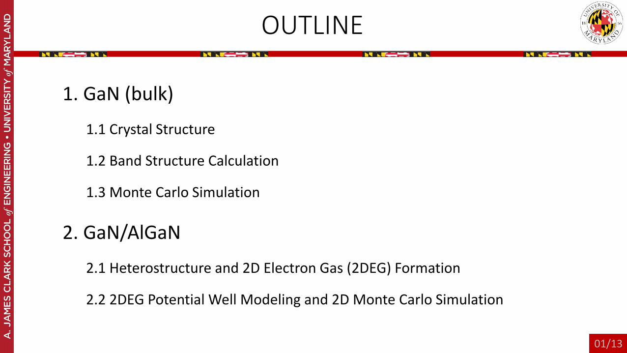
OUTLINE
1. GaN (bulk)
1.1 Crystal Structure
1.2 Band Structure Calculation
1.3 Monte Carlo Simulation
2. GaN/AlGaN
2.1 Heterostructure and 2D Electron Gas (2DEG) Formation
2.2 2DEG Potential Well Modeling and 2D Monte Carlo Simulation
01/13
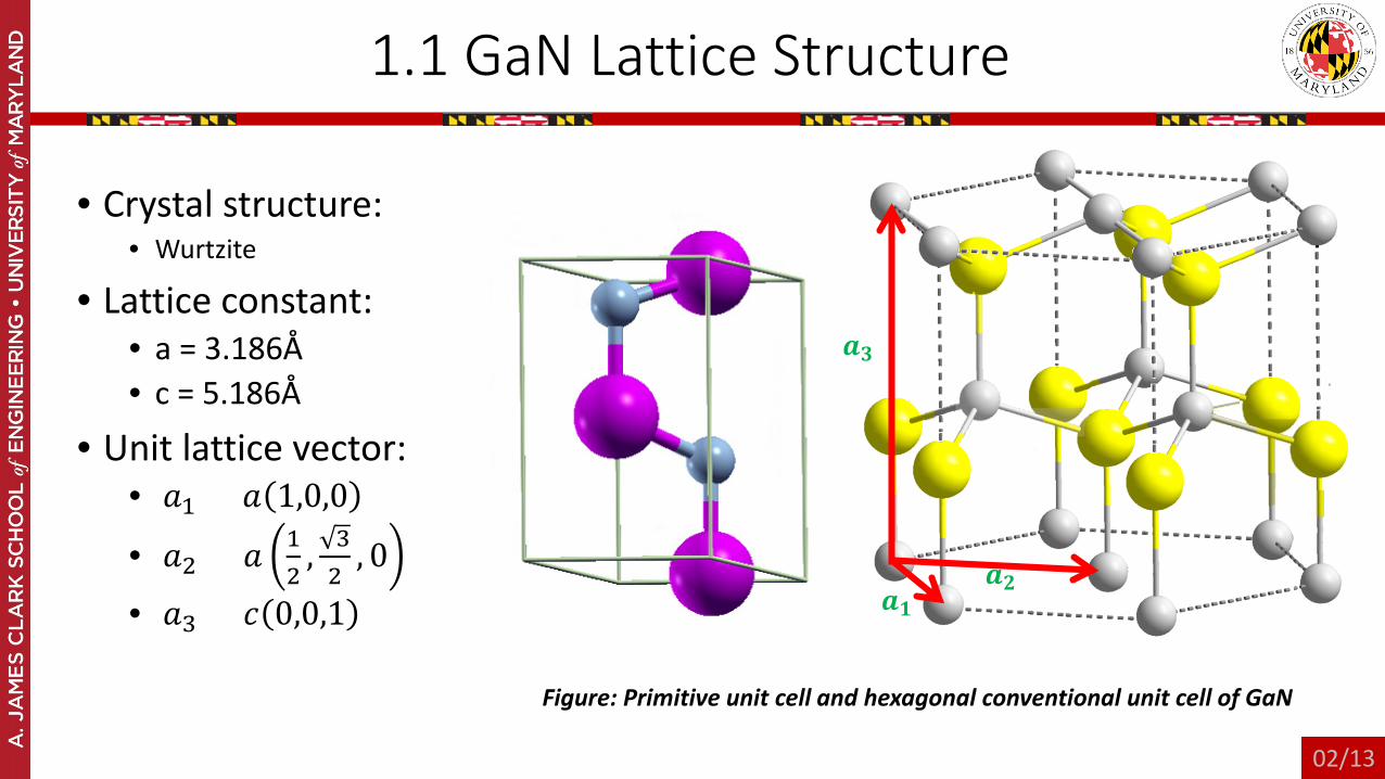
1.1 GaN Lattice Structure
• Crystal structure: • Wurtzite
• Lattice constant: • a = 3.186Å• c = 5.186Å
• Unit lattice vector:• 𝑎𝑎1 = 𝑎𝑎 1,0,0
• 𝑎𝑎2 = 𝑎𝑎 12
, 32
, 0
• 𝑎𝑎3 = 𝑐𝑐 0,0,1
Figure: Primitive unit cell and hexagonal conventional unit cell of GaN
02/13
𝒂𝒂𝟏𝟏𝒂𝒂𝟐𝟐
𝒂𝒂𝟑𝟑
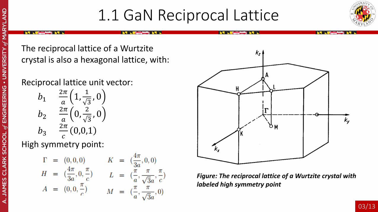
1.1 GaN Reciprocal Lattice
The reciprocal lattice of a Wurtzitecrystal is also a hexagonal lattice, with:
Reciprocal lattice unit vector:𝑏𝑏1 = 2𝜋𝜋
𝑎𝑎1, 1
3, 0
𝑏𝑏2 = 2𝜋𝜋𝑎𝑎
0, 23
, 0
𝑏𝑏3 = 2𝜋𝜋𝑐𝑐
0,0,1High symmetry point:
Figure: The reciprocal lattice of a Wurtzite crystal with labeled high symmetry point
03/13
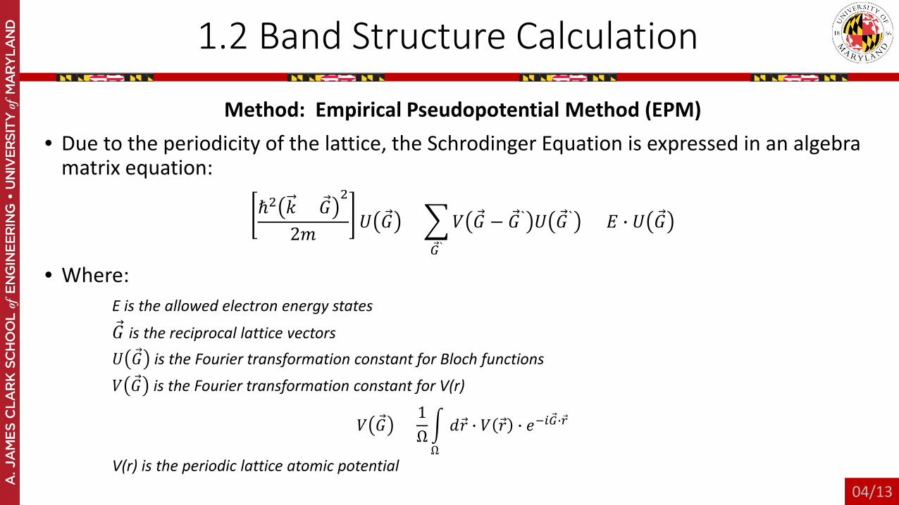
1.2 Band Structure Calculation
Method: Empirical Pseudopotential Method (EPM)• Due to the periodicity of the lattice, the Schrodinger Equation is expressed in an algebra
matrix equation:
ℏ2 𝑘𝑘 + 𝐺2
2𝑚𝑚𝑈𝑈 𝐺 +
𝐺`
𝑉𝑉 𝐺 − 𝐺 ` 𝑈𝑈 𝐺` = 𝐸𝐸 𝑈𝑈 𝐺
• Where:E is the allowed electron energy states
𝐺 is the reciprocal lattice vectors𝑈𝑈 𝐺 is the Fourier transformation constant for Bloch functions
𝑉𝑉 𝐺 is the Fourier transformation constant for V(r)
𝑉𝑉 𝐺 =1ΩΩ
𝑑𝑑𝑟𝑟 𝑉𝑉 𝑟𝑟 𝑒𝑒−𝑖𝑖𝐺𝑟𝑟
V(r) is the periodic lattice atomic potential04/13
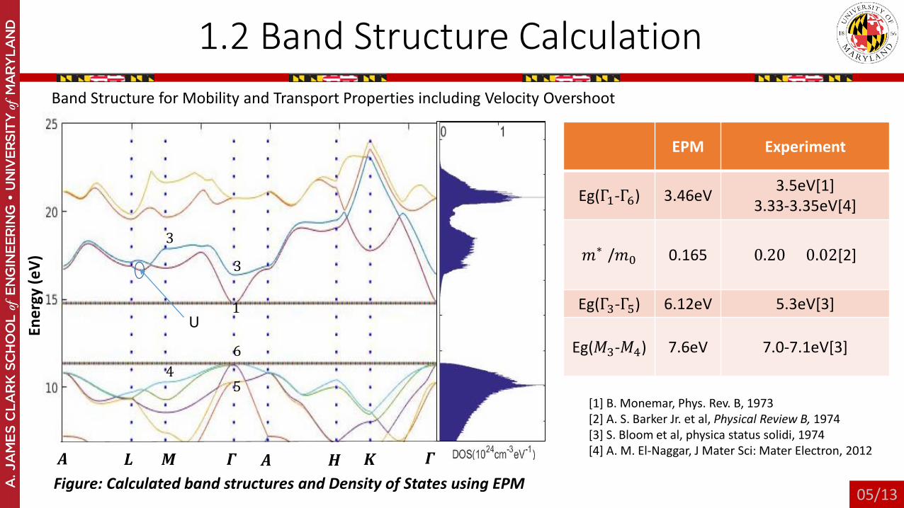
1.2 Band Structure Calculation
EPM Experiment
Eg(Γ1-Γ6) 3.46eV 3.5eV[1]3.33-3.35eV[4]
𝑚𝑚∗ /𝑚𝑚0 0.165 0.20 ± 0.02[2]
Eg(Γ3-Γ5) 6.12eV 5.3eV[3]
Eg(𝑀𝑀3-𝑀𝑀4) 7.6eV 7.0-7.1eV[3]
[1] B. Monemar, Phys. Rev. B, 1973[2] A. S. Barker Jr. et al, Physical Review B, 1974[3] S. Bloom et al, physica status solidi, 1974[4] A. M. El-Naggar, J Mater Sci: Mater Electron, 2012
Band Structure for Mobility and Transport Properties including Velocity Overshoot
05/13
𝑨𝑨 𝑳𝑳 𝑴𝑴 𝜞𝜞 𝑨𝑨 𝑯𝑯 𝑲𝑲 𝜞𝜞Figure: Calculated band structures and Density of States using EPM
Ener
gy (e
V)
U1
6
5
3
4
3
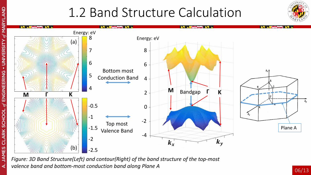
1.2 Band Structure Calculation
Figure: 3D Band Structure(Left) and contour(Right) of the band structure of the top-most valence band and bottom-most conduction band along Plane A
(a)
(b)
Plane A
Bottom mostConduction Band
Top most Valence Band
ΓM K
Energy: eV8
7
6
5
4
-0.5
-1
-1.5
-2
-2.5
Bandgap
Energy: eV
8
6
4
2
0
-4
-2
Γ KM
06/13
𝒌𝒌𝒙𝒙 𝒌𝒌𝒚𝒚
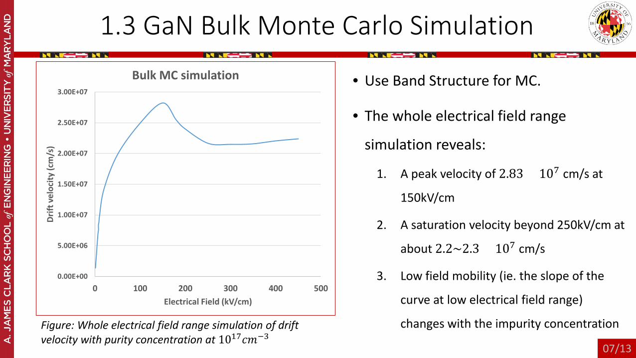
1.3 GaN Bulk Monte Carlo Simulation
• Use Band Structure for MC.
• The whole electrical field range
simulation reveals:
1. A peak velocity of 2.83 × 107 cm/s at
150kV/cm
2. A saturation velocity beyond 250kV/cm at
about 2.2~2.3 × 107 cm/s
3. Low field mobility (ie. the slope of the
curve at low electrical field range)
changes with the impurity concentration
0.00E+00
5.00E+06
1.00E+07
1.50E+07
2.00E+07
2.50E+07
3.00E+07
0 100 200 300 400 500
Drift
vel
ocity
(cm
/s)
Electrical Field (kV/cm)
Bulk MC simulation
Figure: Whole electrical field range simulation of drift velocity with purity concentration at 1017𝑐𝑐𝑚𝑚−3
07/13
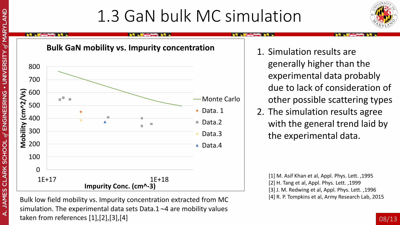
1.3 GaN bulk MC simulation
Bulk low field mobility vs. Impurity concentration extracted from MC simulation. The experimental data sets Data.1∼4 are mobility values taken from references [1],[2],[3],[4]
1. Simulation results are generally higher than the experimental data probably due to lack of consideration of other possible scattering types
2. The simulation results agree with the general trend laid by the experimental data.
0
100
200
300
400
500
600
700
800
1E+17 1E+18
Mob
ility
(cm
^2/V
s)
Impurity Conc. (cm^-3)
Bulk GaN mobility vs. Impurity concentration
Monte CarloData. 1Data.2Data.3Data.4
[1] M. Asif Khan et al, Appl. Phys. Lett. ,1995[2] H. Tang et al, Appl. Phys. Lett. ,1999 [3] J. M. Redwing et al, Appl. Phys. Lett. ,1996[4] R. P. Tompkins et al, Army Research Lab, 2015
08/13
OUTLINE
1. GaN
1.1 Crystal Structure
1.2 Band Structure Calculation
1.3 Monte Carlo Simulation
2. GaN/AlGaN
2.1 Heterostructure and 2D Electron Gas (2DEG) Formation
2.2 2DEG Potential Well Modeling and 2D Monte Carlo Simulation
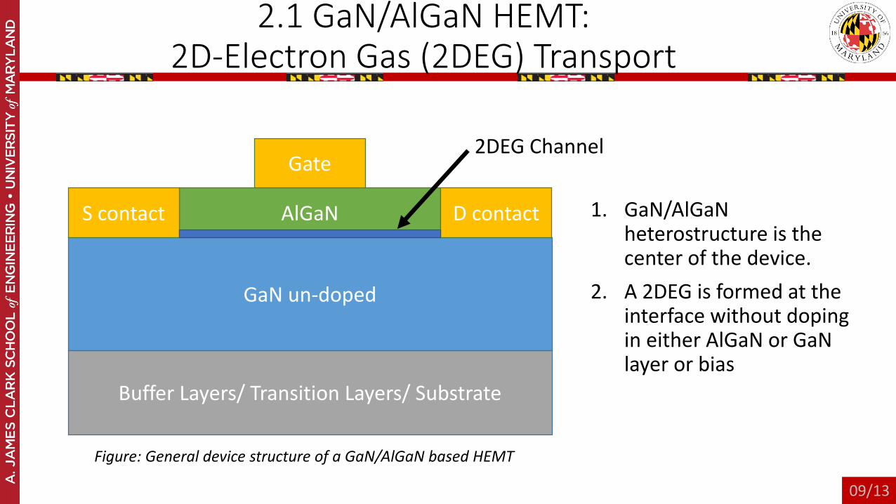
2.1 GaN/AlGaN HEMT:2D-Electron Gas (2DEG) Transport
1. GaN/AlGaNheterostructure is the center of the device.
2. A 2DEG is formed at the interface without doping in either AlGaN or GaNlayer or bias
Buffer Layers/ Transition Layers/ Substrate
GaN un-doped
AlGaNS contact D contact
Gate
Figure: General device structure of a GaN/AlGaN based HEMT
2DEG Channel
09/13
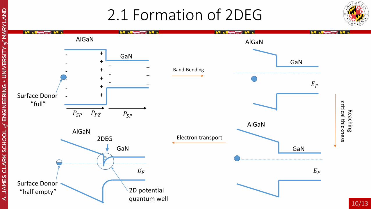
2.1 Formation of 2DEG
Band-Bending
Electron transport
-
AlGaN
GaN
𝑃𝑃𝑆𝑆𝑆𝑆 + 𝑃𝑃𝑆𝑆𝑃𝑃 𝑃𝑃𝑆𝑆𝑆𝑆
++++++
------
---
+++
Reaching critical thickness
𝐸𝐸𝐹𝐹
AlGaN
GaN
𝐸𝐸𝐹𝐹
AlGaN
GaN
𝐸𝐸𝐹𝐹
AlGaN
GaN
Surface Donor”full”
Surface Donor”half empty”
2DEG
10/13
2D potential quantum well
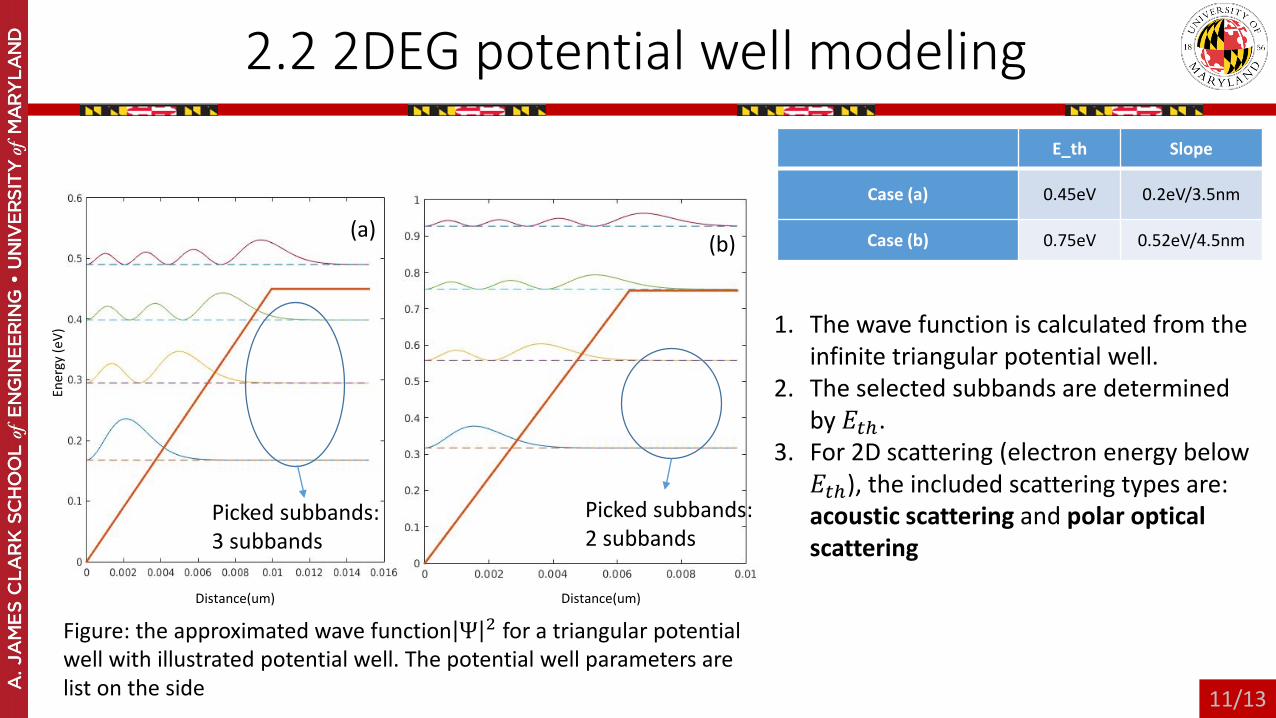
2.2 2DEG potential well modeling
(a)
Ener
gy (e
V)
Distance(um)
Picked subbands:3 subbands
(b)
Distance(um)
Picked subbands:2 subbands
Figure: the approximated wave function Ψ 2 for a triangular potential well with illustrated potential well. The potential well parameters are list on the side
E_th Slope
Case (a) 0.45eV 0.2eV/3.5nm
Case (b) 0.75eV 0.52eV/4.5nm
1. The wave function is calculated from the infinite triangular potential well.
2. The selected subbands are determined by 𝐸𝐸𝑡𝑡𝑡.
3. For 2D scattering (electron energy below 𝐸𝐸𝑡𝑡𝑡), the included scattering types are: acoustic scattering and polar optical scattering
11/13
2.2 2DEG Monte Carlo simulation
Figure: (a)Mean drift electron velocity vs. Electrical field. (b) collections of experimental data for 2DEG mobility and the results of 2D MC simulation from this work. The experimental data sets Data.1∼8 are mobility values taken from references [5],[6],[7],[8],[9],[10],[11],[12]
0.0E+0
5.0E+6
1.0E+7
1.5E+7
2.0E+7
2.5E+7
3.0E+7
0 100 200 300 400 500
Mea
n ve
loci
ty (c
m/s
)
E field(kV/cm)
Mean velocity
Case(a)
Case(b)
3D
(a)
0
500
1000
1500
2000
2500
0.00E+00 2.00E+13 4.00E+13
Mob
ility
(cm
^2/V
s)Electron Sheet Density (cm^-2)
2DEG mobility vs. electron concentration
Data.1Data.2Data.3Data.4Data.5Data.6Data.7Data.8Case(a)Case(b)
(b)
[5] R. Gaska et al. Appl. Phys. Lett., 1998 [6] Y.-F. Wu et al, Appl. Phys. Lett. ,1996 [7] J. M. Redwing et al, Appl. Phys. Lett. ,1996[8] F. Recht et al, IEEE Electron Device Letters, 2006 [9] H. Tang, Appl. Phys. Lett., 1999[10] R. P. Tompkins et al, Army Research Lab, 2015[11] S. Acar et al, Thin Solid Films, 2007[12] O. Katz et al, IEEE Transactions on Electron Devices, 2003
12/13
1. GaN band structure calculation gives good agreement with experimental data
and/or first principle calculations.
2. GaN bulk Monte Carlo Simulation gives agreeable results comparing to
experimental data with a positive offset indicating needs to include more
scattering mechanisms
3. 2D Electron Gas Monte Carlo simulation gives results within the range of the
experimental data collections
4. Bulk GaN Mobility ranges from 500 to 750 𝑐𝑐𝑚𝑚2/𝑉𝑉𝑉𝑉 in our simulation, while 2DEG
mobility is around 1500 - 1700 𝑐𝑐𝑚𝑚2/𝑉𝑉𝑉𝑉.
Conclusion
13/13

Thank you!Any questions?
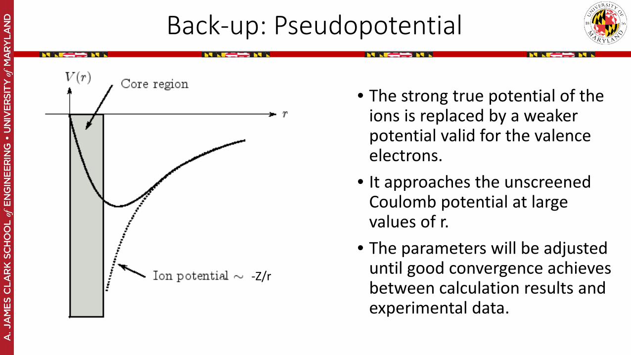
• The strong true potential of the ions is replaced by a weaker potential valid for the valence electrons.
• It approaches the unscreened Coulomb potential at large values of r.
• The parameters will be adjusted until good convergence achieves between calculation results and experimental data.
-Z/r
Back-up: Pseudopotential
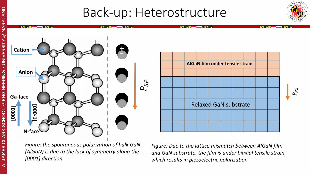
Back-up: Heterostructure
Relaxed GaN substrate
AlGaN film under tensile strain
𝑃𝑃 𝑆𝑆𝑃𝑃
-+
Figure: the spontaneous polarization of bulk GaN(AlGaN) is due to the lack of symmetry along the [0001] direction
Figure: Due to the lattice mismatch between AlGaN film and GaN substrate, the film is under biaxial tensile strain, which results in piezoelectric polarization
Cation
Anion
[000
1]
[000-1]
Ga-face
N-face
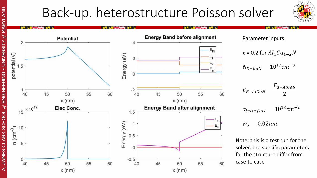
Back-up. heterostructure Poisson solver
Parameter inputs:
x = 0.2 for 𝐴𝐴𝐴𝐴𝑥𝑥𝐺𝐺𝑎𝑎1−𝑥𝑥𝑁𝑁
𝑁𝑁𝐷𝐷−𝐺𝐺𝑎𝑎𝐺𝐺 = 1017𝑐𝑐𝑚𝑚−3
𝐸𝐸𝐹𝐹−𝐴𝐴𝐴𝐴𝐺𝐺𝑎𝑎𝐺𝐺 =𝐸𝐸𝑔𝑔−𝐴𝐴𝐴𝐴𝐺𝐺𝑎𝑎𝐺𝐺
2
𝜎𝜎𝑖𝑖𝑖𝑖𝑡𝑡𝑖𝑖𝑟𝑟𝑖𝑖𝑎𝑎𝑐𝑐𝑖𝑖 = 1013𝑐𝑐𝑚𝑚−2
𝑤𝑤𝜎𝜎 = 0.02𝑛𝑛𝑚𝑚
Note: this is a test run for the solver, the specific parameters for the structure differ from case to case


![Real-space pseudopotential method for noncollinear ... · D.Naveh,L.Kronik/SolidStateCommunications149(2009)177 180 179 previousresults[6],wechoseanequilateraltrianglewithabond lengthof2.1](https://img.pdfslide.net/doc/110x75/5ffdbd7360517352d467ddfc/real-space-pseudopotential-method-for-noncollinear-dnavehlkroniksolidstatecommunications1492009177.jpg)


![Chapter 8 Relativistic Pseudopotential Calculations for ...Relativistic Pseudopotential Calculations for Electronic Excited States ... book [1], it remains to go closely into the matter](https://img.pdfslide.net/doc/110x75/5e42d73cef5ee31dd0652d7c/chapter-8-relativistic-pseudopotential-calculations-for-relativistic-pseudopotential.jpg)


