Embed Size (px)
Citation preview
1
Gate Drive Card for High Power Three Phase PWMConverters
Anil Kumar Adapa Vinod JohnEngineer R&D Department of Electrical Engineering
Medha Servo Drive Pvt. Ltd., India Indian Institute of Science, IndiaEmail: [email protected] Email: [email protected]
Abstract—Gate driver is an integral part of every powerconverter, drives the power semiconductor devices and alsoprovides protection for the switches against short-circuitevents and over-voltages during shut down. Gate drivecard for IGBTs and MOSFETs with basic features canbe designed easily by making use of discrete electroniccomponents. Gate driver ICs provides attractive featuresin a single package, which improves reliability and reduceseffort of design engineers. Either case needs one or moreisolated power supplies to drive each power semiconductordevices and provide isolation to the control circuitry fromthe power circuit. The primary emphasis is then to providesimplified and compact isolated power supplies to the gatedrive card with the requisite isolation strength and whichconsumes less space, and for providing thermal protectionto the power semiconductor modules for 3-φ 3 wire or 4wire inverters.
Index Terms—Gate drive, multi-channel isolated powersupply, thermal protection.
I. INTRODUCTION
G ate drive card converts logic level turn on/off com-mands from the PWM converter to proper power
level signals for reliable control of the power semi-conductor devices. These gate drive cards should pro-tect power semiconductor switches against short circuitevents [1]. In applications, short circuit can happen dueto bad wiring/load, turning on complementary devicesin a leg and cross conduction due to insufficient deadtime. By monitoring VCE(sat) of the IGBT, it is possibleto prevent destruction of the device due to desaturation.Very high currents through the device results in raise ofVCE(sat) and the device dissipates excessive power andfails due to thermal break down. Insufficient gate drivevoltage also leads to desaturation of the device which isundesirable [2]. Rapid turn off of an IGBT under faultleads to failure of the device because of higher voltagestresses due to large di/dt induced voltages, soft turn-offwill prevent such failure.
Commercial gate drive cards provide attractive fea-tures like soft turn off after desaturation fault detection,
under voltage lockout, fault indication with isolation etc.[3]. Gate driver ICs also provide such features in a singlepackage which reduces the effort of design engineers todevelop gate drive cards. Power semiconductor devicesof a converter will have different potential referencenodes and the reference potential of these nodes canvary depending on the switch state, which demandsand isolated power supply per device connected to thedifferent reference nodes. A primary challenge in apractical implementation of a gate drive card is poweringof the gate driver with floating potential references [4].An additional requirement in designing a gate drive cardis to provide isolated power supplies in a small area andwith high reliability. This paper presents a simple powersupply configuration for the design of gate drive cardsfor poly-phase inverters and for providing semiconductorthermal protection by making use of a thermistor basedtemperature sensor.
II. GATE DRIVE CARD
Basic requirements to design a gate drive card are:1) Number of channels and selection of driver IC.2) Requirement of isolated power supplies and their
rating.-Gate voltage levels-Gate charge estimation-Peak current requirement
3) Provision for isolated power supplies.A gate drive card has been designed with 6 driver
channels, which can be extended upto 8 channels. Thegate drive card makes use of AVAGO technologiesHCPL-316J gate driver IC [5]. Block diagram of thedesigned gate drive card, shown in Fig. 2, indicates thearrangement of the gate drive channels, power supplyand temperature sensing sections. Each channel requirestwo isolated power supplies and one non-isolated powersupply whose ground is same as that of the systemcontrol ground reference. Each channel is designed todeliver at least 2 W of average power to the gate circuit

2
B B
2.2k
Fig. 1. Schematic of one channel of the gate drive. The sections identified are: (A) High frequency transformer for isolation; (B) Isolatedpower supplies for the gate drive card; (C) Primary side of the gate driver powered with +5V non-isolated supply with signal or controllerground; and (D) output peak current boosters.
Fig. 2. Block diagram of the gate drive card for a 3−φ 3 leg inverter.
including the gate resistor, with a peak current capacityof 8 A. To increase peak gate current of 8 A npn/pnpswitching transistor buffer is used. This allows the gatedrive card to be used in the design of high powerinverters. Schematic of one channel of the designed gatedrive card is shown in Fig. 1.
III. POWER SUPPLY
Isolated power supplies can be provided usingswitched mode power converters. With increasing con-verter switching frequency, the size of the magneticcircuit and output charge reserve capacitor comes down.Though wide varieties of switched mode power convert-ers are possible each has its own merits and limitations.Fly back converter is simple and has less number ofcomponents compared other types of converters. Suchconverters are used in many cases where the requirementis for low power of less than 10 W , with isolation.It suffers from inevitable higher voltage stresses acrossthe switches and produces switching noise because ofringing across the diodes. Providing many power sup-plies using fly back converters is not advisable. Suchneed exists in poly-phase inverters for 3 wire and 4wire applications. Another option, that is investigated inthis paper, is to generate many isolated power supply
Fig. 3. Schematic showing the isolated power supply for a channelof the gate drive card.
channels with in a small area is using high frequencyAC square wave voltage source and small toroidal ferritetransformers.
1) High frequency inverter: For the designed gatedrive card, a 200 kHz half bridge inverter has beendesigned to power all the gate drive channels. The useof the half bridge topology ensures that there is nochance of saturation in the core of transformers as thereis no path for circulating DC current. Using a smalltoroidal transformer of less than 16 mm outer diameter,with one primary and two secondary windings has beendesigned to supply dual voltages at 4 W power level.A high level schematic of the isolated power supplybased on a half-bridge inverter is shown in Fig. 3.The secondary low voltage side of the power supplyconsists of a voltage doubler circuit, which requiresfewer turns and with a single diode drop in the circuitpath. Gate turn on and turn off voltage levels can beadjusted easily by changing number of secondary turnsof the transformer. For additional isolated power supplychannels only the high frequency transformer and thediodes on the secondary are duplicated. Hence, onlytwo active switches are required for generating isolatedsupplies for all the channels of a poly-phase inverter.
3
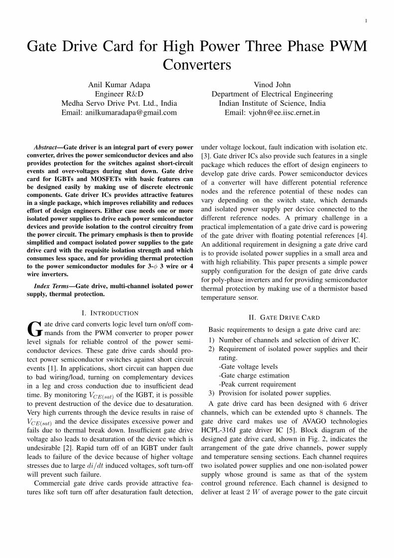
A. Design of the Transformer
The high frequency transformer core selection hasbeen done based on area product calculation [6],
AcAw =V A
4fBmkwJ(in mm4) (1)
whereV A : transformer volt ampere rating (8 V A)f : frequency of operation (200 kHz)Bm : peak operating flux density (0.1 T )kw : window factor (0.05)J : current density of (2.2 A/mm2)
A low value of window factor, with kw taken to be0.3 is used in this case because PVC coated strandedconductors are for achieving high voltage isolation lev-els. These conductors area is approximately 4 times thebare copper conductor area. A small plastic partition ofwidth 0.5 mm is used to physically separate the pri-mary and secondary windings, again to obtain adequatecreepage distance between the windings. This partitionalso occupies an area of window that is comparable tothe windings because of very small core size used inthis application. Isolation voltage between primary andsecondary is greater than 1.55 kV peak with a minimumair gap of 0.5 mm at all points along the isolation barrierin the power supply channels. Calculated transformerarea product is 909 mm4, EPCOS R15×10.4×5.3 ferritecore is selected. It has an area product of 1023 mm4 andarea of cross-section of 12.05 mm2.
To select the primary winding turns, Np1, a 10% dropin V1 has been considered assuming that the leakageinductance of primary winding is be around 10%. Twoisolated dc supplies are derived using voltage doublers.A linear regulator has been used for positive supply of+15 V in each channel. An unregulated negative supplyfrom the second voltage doubler has been used for thenegative bias of −5 V for each gate drive channel.Unregulated input voltage to the linear regulator shouldbe at least 3V higher than that of its output. This isused to obtain the turns requirement of the secondarywindings.
Vs =dc output, Vdc
2+Diode drop, VD
Vs1 =18V
2+ 0.5V = 9.5 V
Vs2 =5V
2+ 0.5V = 3 V
(2)
Number of turns are,
Np1 =Vp1
4fBmAc≈ 11
Ns1 =Vs1
4fBmAc≈ 10
Ns2 =Vs2
4fBmAc≈ 3
(3)
Fig. 4. Principle of thermistor based temperature sensor, with a lookup table used for the dependence of the resistance with temperature.
Fig. 5. Modelling of the semiconductor module and heat sink of apower converter to obtain the junction temperature.
Fig. 6. Thermistor based thermal protection. The voltage VTH isused to calculate the power device junction temperature.
IV. THERMAL PROTECTION
In addition to over-current protection, the power con-verter needs to shut down in case the junction tempera-ture exceeds the semiconductors rated maximum level of1500C. It is common to sense the heat-sink temperature,or power semiconductor device case temperature whensuch as option is available, and to use it as a scaledestimate of the junction temperature and to initiateconverter shut down.
If temperature sensors such as thermocouples andRTD are used, the noise generated during the switchingoperation of the power converter will corrupt the smallvoltage levels of these sensors easily. Hence, for satisfac-torily temperature sensing in such inverter environments,
4
a sensor with high signal level is advantageous. In spiteof non-linear resistance variation with temperature, ther-mistor based temperature sensors can serve well in thissituation because of its high sensitivity to temperature.Modern power semiconductor modules available todayare having thermistors embedded inside the module withdouble bonded copper insulation [7], [8]. A constantcurrent source and thermistor based temperature sensecircuit, as shown in Fig. 4, has been used in the gatedrive circuit. By driving small current of the orderof 1 mA through the thermistor and monitoring thevoltage across its terminals, it is possible to extract thetemperature information at the base plate of the powersemiconductor module. This can be considered to bethe case temperature, Tc, of the module. Temperatureof the heat sink of the inverter can be found usingexternal thermistor mounted on the heat sink. Once thisinformation is made available to the processor, from theheat sink modelling and resistance-temperature profileof the thermistor, fast temperature information can beobtained, which can be used on a sub-cycle basis forthermal protection.
Referring to the thermal model of the semiconductordevice and heat sink arrangement shown in Fig. 5, Tjis the junction temperature of the device and Ts is theheat sink temperature. Rth(j−s) is junction to heat sinkthermal resistance. Rth(s−a) is heat sink to ambient ther-mal resistance. From the resistance information of thethermistor R(T ) and using a look-up table, temperatureof the case Tc, or heat sink Ts, can be obtained. From thethermal model of the heat sink, the junction temperatureof the module is as given in eq.(5).
The resistance of the thermistor can be modelled as,
R(T ) = R0eB( 1
T− 1
T0) (4)
Where R(T ) is resistance of the thermistor at atemperature of T degrees K, R0 is resistance of thethermistor at a temperature of T0K, and B is a constantspecified in datasheet [8].
Tj(t) = Ts(t)
(1 +
Rth(j−s)
Rth(s−a)
)+ CsRth(j−s)
dTsdt
(5)
For a given thermistor current bias, the terminal volt-age VTH is used with a lookup table to provide a readoutof the case temperature as shown in Fig. 6.
V. RESULTS
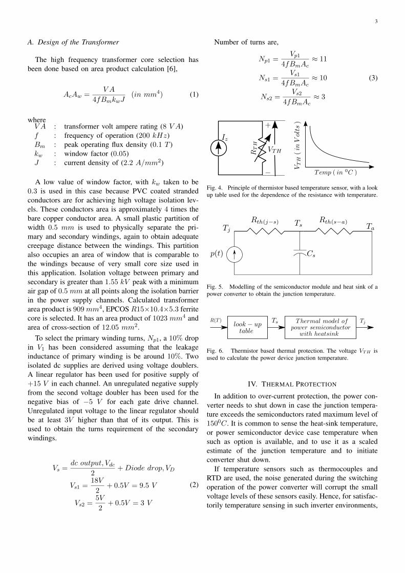
The designed gate drive card has been tested for itspeak current delivery. With +15 V gate turn on voltageand −5 V gate turn off voltage, 2 Ω turn on and turnoff gate resistors and with a capacitive load of 470 nF
(a) Turn-on gate current
(b) Turn-off gate current
Fig. 7. Peak current test on gate drive card. CH1 : In-put PWM pulse (2V/div) and CH2 : Gate current, IG (5A/div) andtime: 500 ns/div.
Fig. 8. Short circuit test on a gate drive channel of the designed gateddrive card. VCE :100V/div, IC :100A/div, VGE :5V/div, FAULT:5V/divand time:500 ns/div.
connected to the gate and emitter terminal of the gatedrive card by a 10 cm long twisted pair of wires, gatecurrents have been captured. These results are shownin Fig. 7. The wire impedance prevented the peak gate

5
Fig. 9. Thermal image of the gate drive card during long termendurance tests.
Fig. 10. Thermal image of output booster stage and gate resistorstage of the designed gate drive card during long term endurancetests.
current from reaching 8 A. This effect of the lead lengthis also expected in the practical laboratory packaging ofthe inverter.
Short circuit test has been performed on the designedgate drive card to test for its functionalities such as desatfault detection, soft turn off during fault shut down. Theresults of the short circuit test are shown in Fig. 8. Toperform this test one leg of the inverter has been operatedas a chopper with light RL-load and then it is shortedusing mechanical contactor. Duty ratio of the pulses arevery low for this case with Ton = 400 µs and Toff =4 ms. In Fig. 8 the IGBT on which this test is performedshows the condition where it has been turned on duringshort circuit conditions. The waveforms indicate that thegate drive card detected the fault after a short blankingtime and then cut-off the gate pulse using soft turn offfeature. The fault is then notified to the controller usingFAULT status by taking the fault output from logichigh to low state. The fault and switching tests has beenperformed with different gate resistors and it is observedthat the gate resistor values have a major influence onthe turn on and turn off process of the IGBT in terms of
Fig. 11. No-load line current waveforms of a 2.3kW , 415V ,4.5A, 1440rpm ∆-connected induction machine used in a 10kWinverter with the gate drive card. CH1 and CH2 : 1.735A/div., time:10ms/div.
Fig. 12. Line current waveforms of a 22kW , 415V , 4.5A, 1475rpm∆-connected induction machine at 10kV A input used in a inverterwith the gate drive card. CH1 and CH2 : 17.35A/div., time:10ms/div.
losses, diode recovery etc. [9].After continuous operation of the gate drive card
for 5 hours while delivering rated power, its thermalimage has been captured and the maximum temperatureon the card is observed as 760C at the output stagegate resistors as shown in Fig. 9 and Fig. 10. Theremaining parts of the gate drive circuit are at less than450C with an ambient temperature of 260C. All othersemiconductor ICs junction temperature will be withinlimits for continuous operation of the designed gate drivecard. Test conditions are, Rg(on) = Rg(off) = 8.2 Ω and300 nF capacitive load was connected using a 10 cmlong twisted pair of lead wires. The switching frequencyof 21 kHz input is applied to dissipate 2 W power inthe gate resistors for the thermal endurance test of thegate drive card.
6
0 500 1000 1500 2000 2500 3000 3500 4000 45000
0.5
1
1.5
2
2.5
3
3.5
4
4.5
5
Resistance of the thermistor, Rth
(in Ω)
Ou
tpu
t o
f th
e th
erm
al c
ard
, V
th (
in V
olt
s)
Linearity test on thermal card
practical
expected
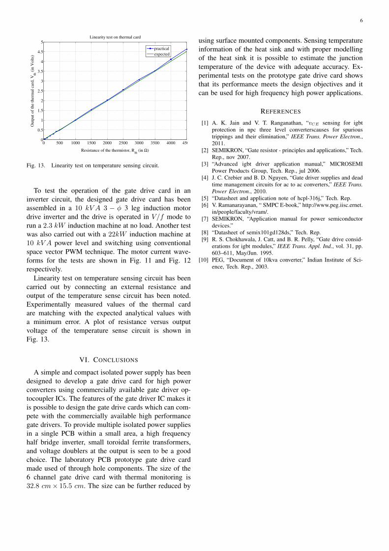
Fig. 13. Linearity test on temperature sensing circuit.
To test the operation of the gate drive card in aninverter circuit, the designed gate drive card has beenassembled in a 10 kV A 3 − φ 3 leg induction motordrive inverter and the drive is operated in V/f mode torun a 2.3 kW induction machine at no load. Another testwas also carried out with a 22kW induction machine at10 kV A power level and switching using conventionalspace vector PWM technique. The motor current wave-forms for the tests are shown in Fig. 11 and Fig. 12respectively.
Linearity test on temperature sensing circuit has beencarried out by connecting an external resistance andoutput of the temperature sense circuit has been noted.Experimentally measured values of the thermal cardare matching with the expected analytical values witha minimum error. A plot of resistance versus outputvoltage of the temperature sense circuit is shown inFig. 13.
VI. CONCLUSIONS
A simple and compact isolated power supply has beendesigned to develop a gate drive card for high powerconverters using commercially available gate driver op-tocoupler ICs. The features of the gate driver IC makes itis possible to design the gate drive cards which can com-pete with the commercially available high performancegate drivers. To provide multiple isolated power suppliesin a single PCB within a small area, a high frequencyhalf bridge inverter, small toroidal ferrite transformers,and voltage doublers at the output is seen to be a goodchoice. The laboratory PCB prototype gate drive cardmade used of through hole components. The size of the6 channel gate drive card with thermal monitoring is32.8 cm× 15.5 cm. The size can be further reduced by
using surface mounted components. Sensing temperatureinformation of the heat sink and with proper modellingof the heat sink it is possible to estimate the junctiontemperature of the device with adequate accuracy. Ex-perimental tests on the prototype gate drive card showsthat its performance meets the design objectives and itcan be used for high frequency high power applications.
REFERENCES
[1] A. K. Jain and V. T. Ranganathan, “vCE sensing for igbtprotection in npc three level converterscauses for spurioustrippings and their elimination,” IEEE Trans. Power Electron.,2011.
[2] SEMIKRON, “Gate resistor - principles and applications,” Tech.Rep., nov 2007.
[3] “Advanced igbt driver application manual,” MICROSEMIPower Products Group, Tech. Rep., jul 2006.
[4] J. C. Crebier and B. D. Nguyen, “Gate driver supplies and deadtime management circuits for ac to ac converters,” IEEE Trans.Power Electron., 2010.
[5] “Datasheet and application note of hcpl-316j,” Tech. Rep.[6] V. Ramanarayanan, “ SMPC E-book,” http://www.peg.iisc.ernet.
in/people/faculty/vram/.[7] SEMIKRON, “Application manual for power semiconductor
devices.”[8] “Datasheet of semix101gd128ds,” Tech. Rep.[9] R. S. Chokhawala, J. Catt, and B. R. Pelly, “Gate drive consid-
erations for igbt modules,” IEEE Trans. Appl. Ind., vol. 31, pp.603–611, May/Jun. 1995.
[10] PEG, “Document of 10kva converter,” Indian Institute of Sci-ence, Tech. Rep., 2003.