Embed Size (px)
Citation preview
○Product structure:Silicon integrated circuit ○This product is not designed protection against radioactive rays
.
1/31
TSZ02201-0717ABH00090-1-2 © 2013 ROHM Co., Ltd. All rights reserved. 20.May.2015 Rev.002 TSZ22111・14・001
www.rohm.com
Gate Driver Providing Galvanic isolation Series
Isolation voltage 2500Vrms 1ch Gate Driver Providing Galvanic Isolation BM6101FV-C
●General Description
The BM6101FV-C is a gate driver with isolation voltage 2500Vrms, I/O delay time of 350ns, and minimum input pulse width of 180ns, and incorporates the fault signal output functions, undervoltage lockout (UVLO) function, thermal protection function, and short current protection (SCP, DESAT) function.
●Features
Providing Galvanic Isolation Active Miller Clamping Fault signal output function
(Adjustable output holding time) Undervoltage lockout function Thermal protection function Short current protection function
(Adjustable reset time) Soft turn-off function for short current protection
(Adjustable turn-off time) Supporting Negative VEE UL1577 Recognized:File No. E356010 AEC-Q100 Qualified
(Note 1)
(Note 1:Grade1)
●Key Specifications
Isolation voltage: 2500Vrms(Max.) Maximum gate drive voltage: 24V(Max.) I/O delay time: 350ns(Max.) Minimum input pulse width: 180ns(Max.)
●Package W(Typ.) x D(Typ.) x H(Max.)
SSOP-B20W 6.50mm x 8.10mm x 2.01mm
●Applications
■ Automotive isolated IGBT/MOSFET inverter gate drive ■ Automotive DC-DC converter ■ Industrial inverters system ■ UPS system
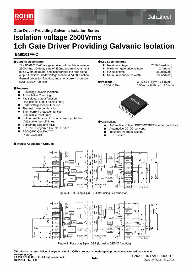
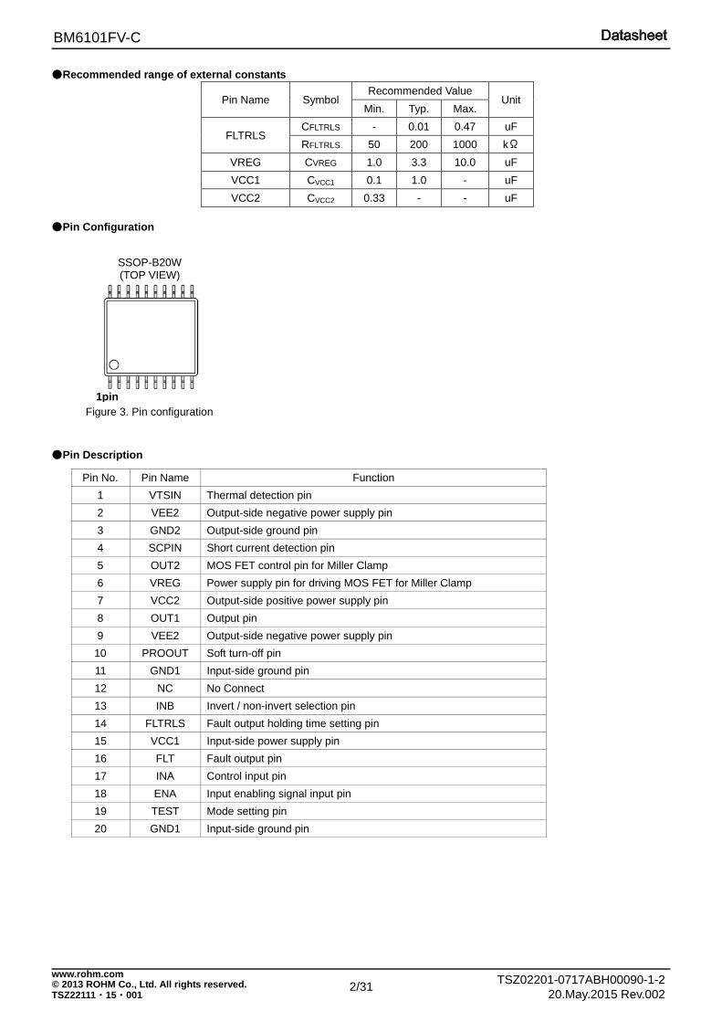
●Typical Application Circuits
R FL
TR
LS
C FL
TR
LS
OUT1
VTSIN
Input side chip
NC
GND1
GND1
INA
TIMER
TIMER
UVLO
FLTRLS
VCC1
Output side chip
TEST VEE2
MASK
VREG
OUT2
FLT
VCC2
LOGIC
S
R
Q
PROOUT
VEE2 PRE DRIVER
MASK
MASK
MASK FB
C VC
C1
C VC
C2
FLT
ENA
ECU
INB
GND2
MASK
LOGIC
MASK
FLT
Temp Sensor
UVLO
SCPIN
VEE2
Figure 1. For using 4-pin IGBT (for using SCP function)
R F
LT
RL
S
C FL
TR
LS
OUT1
VTSIN
Input side chip
NC
GND1
GND1
INA
TIMER
TIMER
UVLO
FLTRLS
VCC1
Output side chip
TEST VEE2
MASK
VREG
OUT2
FLT
VCC2
LOGIC
S
R
Q
PROOUT
VEE2 PRE DRIVER
MASK
MASK
MASK FB
C V
CC
1
C V
CC
2
FLT
ENA
ECU
INB
GND2
MASK
LOGIC
MASK
FLT
Temp Sensor
UVLO
SCPIN
VEE2
Figure 2. For using 3-pin IGBT (for using DESAT function)
Datasheet
2/31
BM6101FV-C
TSZ02201-0717ABH00090-1-2 © 2013 ROHM Co., Ltd. All rights reserved. 20.May.2015 Rev.002
www.rohm.com
TSZ22111・15・001
●Recommended range of external constants
Pin Name Symbol Recommended Value
Unit Min. Typ. Max.
FLTRLS CFLTRLS - 0.01 0.47 uF
RFLTRLS 50 200 1000 kΩ
VREG CVREG 1.0 3.3 10.0 uF
VCC1 CVCC1 0.1 1.0 - uF
VCC2 CVCC2 0.33 - - uF
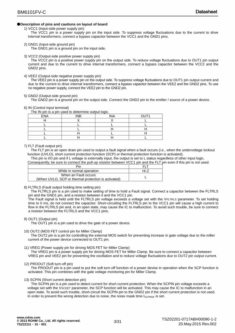
●Pin Configuration ●Pin Description
Pin No. Pin Name Function
1 VTSIN Thermal detection pin
2 VEE2 Output-side negative power supply pin
3 GND2 Output-side ground pin
4 SCPIN Short current detection pin
5 OUT2 MOS FET control pin for Miller Clamp
6 VREG Power supply pin for driving MOS FET for Miller Clamp
7 VCC2 Output-side positive power supply pin
8 OUT1 Output pin
9 VEE2 Output-side negative power supply pin
10 PROOUT Soft turn-off pin
11 GND1 Input-side ground pin
12 NC No Connect
13 INB Invert / non-invert selection pin
14 FLTRLS Fault output holding time setting pin
15 VCC1 Input-side power supply pin
16 FLT Fault output pin
17 INA Control input pin
18 ENA Input enabling signal input pin
19 TEST Mode setting pin
20 GND1 Input-side ground pin
Figure 3. Pin configuration
SSOP-B20W (TOP VIEW)
1pin
3/31
BM6101FV-C
TSZ02201-0717ABH00090-1-2 © 2013 ROHM Co., Ltd. All rights reserved. 20.May.2015 Rev.002
www.rohm.com
TSZ22111・15・001
●Description of pins and cautions on layout of board
1) VCC1 (Input-side power supply pin) The VCC1 pin is a power supply pin on the input side. To suppress voltage fluctuations due to the current to drive
internal transformers, connect a bypass capacitor between the VCC1 and the GND1 pins. 2) GND1 (Input-side ground pin)
The GND1 pin is a ground pin on the input side. 3) VCC2 (Output-side positive power supply pin)
The VCC2 pin is a positive power supply pin on the output side. To reduce voltage fluctuations due to OUT1 pin output current and due to the current to drive internal transformers, connect a bypass capacitor between the VCC2 and the GND2 pins.
4) VEE2 (Output-side negative power supply pin)
The VEE2 pin is a power supply pin on the output side. To suppress voltage fluctuations due to OUT1 pin output current and due to the current to drive internal transformers, connect a bypass capacitor between the VEE2 and the GND2 pins. To use no negative power supply, connect the VEE2 pin to the GND2 pin.
5) GND2 (Output-side ground pin)
The GND2 pin is a ground pin on the output side. Connect the GND2 pin to the emitter / source of a power device. 6) IN (Control input terminal)
The IN pin is a pin used to determine output logic.
ENA INB INA OUT1
H X X L
L L L L
L L H H
L H L H
L H H L
7) FLT (Fault output pin)
The FLT pin is an open drain pin used to output a fault signal when a fault occurs (i.e., when the undervoltage lockout function (UVLO), short current protection function (SCP) or thermal protection function is activated).
This pin is I/O pin and if L voltage is externally input, the output is set to L status regardless of other input logic. Consequently, be sure to connect the pull-up resistor between VCC1 pin and the FLT pin even if this pin is not used.
Pin FLT
While in normal operation Hi-Z When an Fault occurs
(When UVLO, SCP or thermal protection is activated) L
8) FLTRLS (Fault output holding time setting pin)
The FLTRLS pin is a pin used to make setting of time to hold a Fault signal. Connect a capacitor between the FLTRLS pin and the GND1 pin, and a resistor between it and the VCC1 pin. The Fault signal is held until the FLTRLS pin voltage exceeds a voltage set with the VFLTRLS parameter. To set holding time to 0 ms, do not connect the capacitor. Short-circuiting the FLTRLS pin to the VCC1 pin will cause a high current to flow in the FLTRLS pin and, in an open state, may cause the IC to malfunction. To avoid such trouble, be sure to connect a resistor between the FLTRLS and the VCC1 pins.
9) OUT1 (Output pin)
The OUT1 pin is a pin used to drive the gate of a power device. 10) OUT2 (MOS FET control pin for Miller Clamp)
The OUT2 pin is a pin for controlling the external MOS switch for preventing increase in gate voltage due to the miller current of the power device connected to OUT1 pin.
11) VREG (Power supply pin for driving MOS FET for Miller Clamp)
The VREG pin is a power supply pin for driving MOS FET for Miller Clamp. Be sure to connect a capacitor between VREG pin and VEE2 pin for preventing the oscillation and to reduce voltage fluctuations due to OUT2 pin output current.
12) PROOUT (Soft turn-off pin)
The PROOUT pin is a pin used to put the soft turn-off function of a power devise in operation when the SCP function is activated. This pin combines with the gate voltage monitoring pin for Miller Clamp.
13) SCPIN (Short current detection pin)
The SCPIN pin is a pin used to detect current for short current protection. When the SCPIN pin voltage exceeds a voltage set with the VSCDET parameter, the SCP function will be activated. This may cause the IC to malfunction in an open state. To avoid such trouble, short-circuit the SCPIN pin to the GND2 pin if the short current protection is not used. In order to prevent the wrong detection due to noise, the noise mask time tSCPMSK is set.
4/31
BM6101FV-C
TSZ02201-0717ABH00090-1-2 © 2013 ROHM Co., Ltd. All rights reserved. 20.May.2015 Rev.002
www.rohm.com
TSZ22111・15・001
14) VTSIN (Thermal detection pin) The VTSIN pin is a temperature sensor voltage input pin, which can be used for thermal protection of an output device.
If VTSIN pin voltage becomes VTSDET or less, OUT pin is set to L. In the open status, the IC may malfunction, so be sure to supply the VTSPIN more than VTSDET if the thermal protection function is not used. In order to prevent the wrong detection due to noise, the noise mask time tTSMSK is set.
15) TEST(Mode setting pin)
The TEST pin is an operation mode setting pin. This pin is usually connected to GND1 pin. If the TEST pin is connected to the VCC1 pin, Input-side UVLO function is disabled.
●Description of functions and examples of constant setting
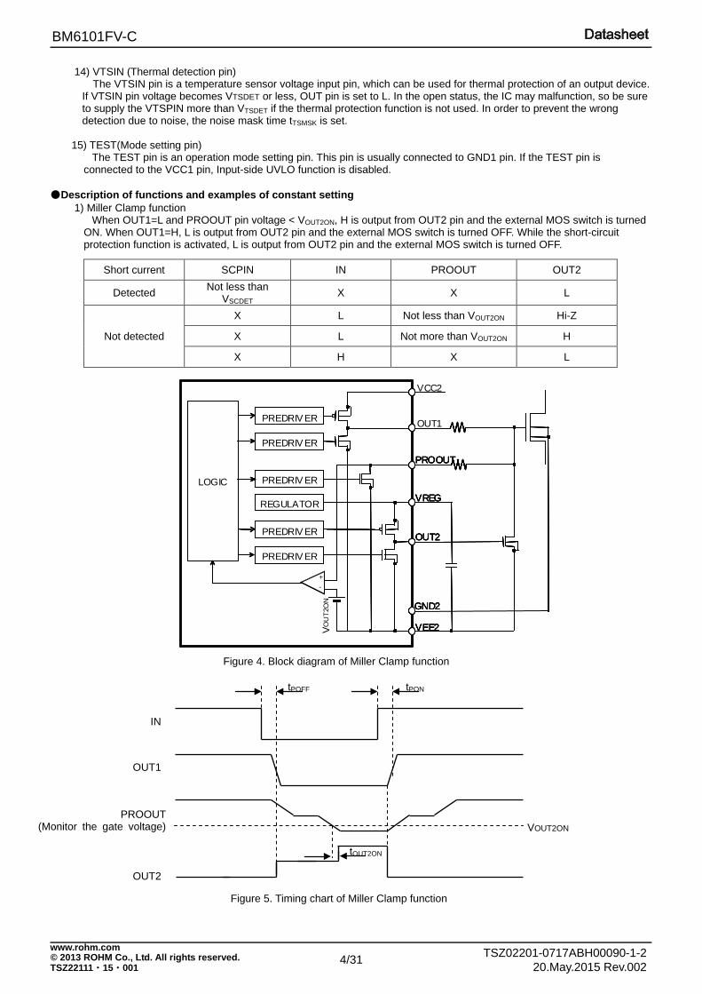
1) Miller Clamp function When OUT1=L and PROOUT pin voltage < VOUT2ON, H is output from OUT2 pin and the external MOS switch is turned
ON. When OUT1=H, L is output from OUT2 pin and the external MOS switch is turned OFF. While the short-circuit protection function is activated, L is output from OUT2 pin and the external MOS switch is turned OFF.
- +
LOGIC
PREDRIV ER PREDRIV ER PREDRIV ER
VCC2 OUT1 PROOUT
GND2 VEE2
V O
UT
2ON
PREDRIV ER PREDRIV ER
OUT2
REGULATOR
VREG
- +
- +
LOGIC
PREDRIV ER PREDRIV ER PREDRIV ER
PROOUT
GND2 VEE2
PREDRIV ER PREDRIV ER
OUT2
REGULATOR
VREG
- +
- +
LOGIC
PREDRIV ER PREDRIV ER PREDRIV ER
PROOUT
GND2 VEE2
PREDRIV ER PREDRIV ER
OUT2
REGULATOR
VREG
- +
- +
LOGIC
PREDRIV ER PREDRIV ER PREDRIV ER
PROOUT
GND2 VEE2
PREDRIV ER PREDRIV ER
OUT2
REGULATOR
VREG
Short current SCPIN IN PROOUT OUT2
Detected Not less than
VSCDET X X L
Not detected
X L Not less than VOUT2ON Hi-Z
X L Not more than VOUT2ON H
X H X L
Figure 4. Block diagram of Miller Clamp function
Figure 5. Timing chart of Miller Clamp function
VOUT2ON
IN
OUT1
PROOUT (Monitor the gate voltage)
OUT2
tPOFF tPON
tOUT2ON
5/31
BM6101FV-C
TSZ02201-0717ABH00090-1-2 © 2013 ROHM Co., Ltd. All rights reserved. 20.May.2015 Rev.002
www.rohm.com
TSZ22111・15・001
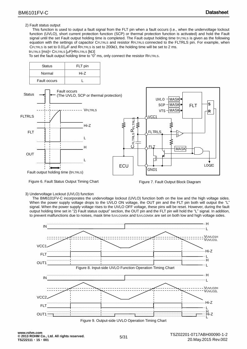
2) Fault status output This function is used to output a fault signal from the FLT pin when a fault occurs (i.e., when the undervoltage lockout
function (UVLO), short current protection function (SCP) or thermal protection function is activated) and hold the Fault signal until the set Fault output holding time is completed. The Fault output holding time tFLTRLS is given as the following equation with the settings of capacitor CFLTRLS and resistor RFLTRLS connected to the FLTRLS pin. For example, when
CFLTRLS is set to 0.01F and RFLTRLS is set to 200k, the holding time will be set to 2 ms.
tFLTRLS [ms]= CFLTRLS [F]•RFLTRLS [k] To set the fault output holding time to “0” ms, only connect the resistor RFLTRLS.
Status FLT pin
Normal Hi-Z
Fault occurs L
3) Undervoltage Lockout (UVLO) function
The BM6101FV-C incorporates the undervoltage lockout (UVLO) function both on the low and the high voltage sides. When the power supply voltage drops to the UVLO ON voltage, the OUT pin and the FLT pin both will output the “L” signal. When the power supply voltage rises to the UVLO OFF voltage, these pins will be reset. However, during the fault output holding time set in “2) Fault status output” section, the OUT pin and the FLT pin will hold the “L” signal. In addition, to prevent malfunctions due to noises, mask time tUVLO1MSK and tUVLO2MSK are set on both low and high voltage sides.
IN L
H
VCC2
VUVLO2H VUVLO2L
FLT Hi-Z
L
OUT1 L
H Hi-Z
Figure 9. Output-side UVLO Operation Timing Chart
Figure 8. Input-side UVLO Function Operation Timing Chart
VCC1
VUVLO1H VUVLO1L
FLT Hi-Z
L
OUT1 L
H
L
H IN
Figure 7. Fault Output Block Diagram
Fig.3 エラー出力ブロック図
ECU
VCC1
FLTRLS
FLT
GND1
R
FLT
RLS
C FL
TR
LS
UVLO SCP VTS
LOGIC
MASK
FLT
MASK MASK MASK
-
- +
R
S
Figure 6. Fault Status Output Timing Chart
FLT
Hi-Z
L
OUT
L
H
VFLTRLS
FLTRLS
Fault output holding time (tFLTRLS)
Status
Fault occurs (The UVLO, SCP or thermal protection)
6/31
BM6101FV-C
TSZ02201-0717ABH00090-1-2 © 2013 ROHM Co., Ltd. All rights reserved. 20.May.2015 Rev.002
www.rohm.com
TSZ22111・15・001
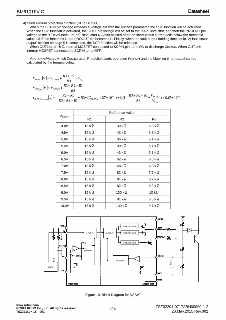
4) Short current protection function (SCP, DESAT) When the SCPIN pin voltage exceeds a voltage set with the VSCDET parameter, the SCP function will be activated.
When the SCP function is activated, the OUT1 pin voltage will be set to the “Hi-Z” level first, and then the PROOUT pin voltage to the “L” level (soft turn-off).Next, after tSTO has passed after the short-circuit current falls below the threshold value, OUT pin becomes L and PROOUT pin becomes L. Finally, when the fault output holding time set in “2) fault status output” section on page 5 is completed, the SCP function will be released.
When OUT1=L or Hi-Z, internal MOSFET connected to SCPIN pin turns ON to discharge CBLANK. When OUT1=H, internal MOSFET connected to SCPIN turns OFF.
VCOLLECTOR/VDRAIN which Desaturation Protection starts operation (VDESAT) and the blanking time (tBLANK) can be
calculated by the formula below;
Figure 10. Block Diagram for DESAT
VDESAT Reference Value
R1 R2 R3
4.0V 15 kΩ 39 kΩ 6.8 kΩ
4.5V 15 kΩ 43 kΩ 6.8 kΩ
5.0V 15 kΩ 36 kΩ 5.1 kΩ
5.5V 15 kΩ 39 kΩ 5.1 kΩ
6.0V 15 kΩ 43 kΩ 5.1 kΩ
6.5V 15 kΩ 62 kΩ 6.8 kΩ
7.0V 15 kΩ 68 kΩ 6.8 kΩ
7.5V 15 kΩ 82 kΩ 7.5 kΩ
8.0V 15 kΩ 91 kΩ 8.2 kΩ
8.5V 15 kΩ 82 kΩ 6.8 kΩ
9.0V 15 kΩ 130 kΩ 10 kΩ
9.5V 15 kΩ 91 kΩ 6.8 kΩ
10.0V 15 kΩ 130 kΩ 9.1 kΩ
6
2
12
outernal
2
1065.0)3
1231ln()1027(3
123
12
3
123
3
23
CC
SCDETBLANKBLANK
SCDETCC
FSCDETDESAT
V
V
R
RRRCR
RRR
RRst
R
RRRVVV
VR
RRVVV
MIN
D
LOGIC
PREDRIVER
PREDRIVER
PREDRIVER
SCPMSK
-
+
LOGIC
-
+
ECU
VCC2
OUT
PROOUT
SCPIN
GND2
VEE2
VCC1
IN
FLTRLS
FLT
GND1
S
R
Input Side Output Side
VTFLTRLS
VS
CD
ET
RF
LT
RL
SC
FL
TR
LS
RSTO
LOGIC
PREDRIVER
PREDRIVER
PREDRIVER
SCPMSK
-
+
-
+
LOGIC
-
+
-
+
ECU
S
R
Input Side Output Side
VTFLTRLS
VS
CD
ET
RSTO
LOGIC
PREDRIVER
PREDRIVER
PREDRIVER
SCPMSK
-
+
-
+
LOGIC
-
+
-
+
ECU
VCC2
OUT
PROOUT
SCPIN
GND2
VEE2
VCC1
IN
FLTRLS
FLT
GND1
S
R
Input Side Output Side
VTFLTRLS
VS
CD
ET
RF
LT
RL
SC
FL
TR
LS
RSTO
LOGIC
PREDRIVER
PREDRIVER
PREDRIVER
SCPMSK
RR1
-
+
-
+
LOGIC
-
+
-
+
ECU
S
R
Input Side Output Side
VTFLTRLS
VS
CD
ET
RSTO
RRRR
23
CB
LA
NK
LOGIC
PREDRIVER
PREDRIVER
PREDRIVER
SCPMSK
-
+
-
+
LOGIC
-
+
-
+
ECU
VCC2
OUT
PROOUT
SCPIN
GND2
VEE2
VCC1
IN
FLTRLS
FLT
GND1
S
R
Input Side Output Side
VTFLTRLS
VS
CD
ET
RF
LT
RL
SC
FL
TR
LS
RSTO
LOGIC
PREDRIVER
PREDRIVER
PREDRIVER
SCPMSK
-
+
-
+
LOGIC
-
+
-
+
ECU
S
R
Input Side Output Side
VTFLTRLS
VS
CD
ET
RSTO
LOGIC
PREDRIVER
PREDRIVER
PREDRIVER
SCPMSK
-
+
-
+
LOGIC
-
+
-
+
ECU
VCC2
OUT
PROOUT
SCPIN
GND2
VEE2
VCC1
IN
FLTRLS
FLT
GND1
S
R
Input Side Output Side
VTFLTRLS
VS
CD
ET
RF
LT
RL
SC
FL
TR
LS
RSTO
LOGIC
PREDRIVER
PREDRIVER
PREDRIVER
SCPMSK
RR1
-
+
-
+
LOGIC
-
+
-
+
ECU
S
R
Input Side Output Side
VTFLTRLS
VS
CD
ET
RSTO
RRRR
23
CB
LA
NK
7/31
BM6101FV-C
TSZ02201-0717ABH00090-1-2 © 2013 ROHM Co., Ltd. All rights reserved. 20.May.2015 Rev.002
www.rohm.com
TSZ22111・15・001
Hi-Z
L Hi-Z
L SCPMSK
スレッショルド
VSCDET
L Hi-Z H VVTLTO H
L
Fault output holding time*7
FLT
PROOUT
SCPIN
OUT1
IN
Hi-Z
L
Hi-Z
L
VSCDET
L Hi-Z H
H
L
tSTO
OUT2 Hi-Z H
L
Fault output holding time *7
tSTO
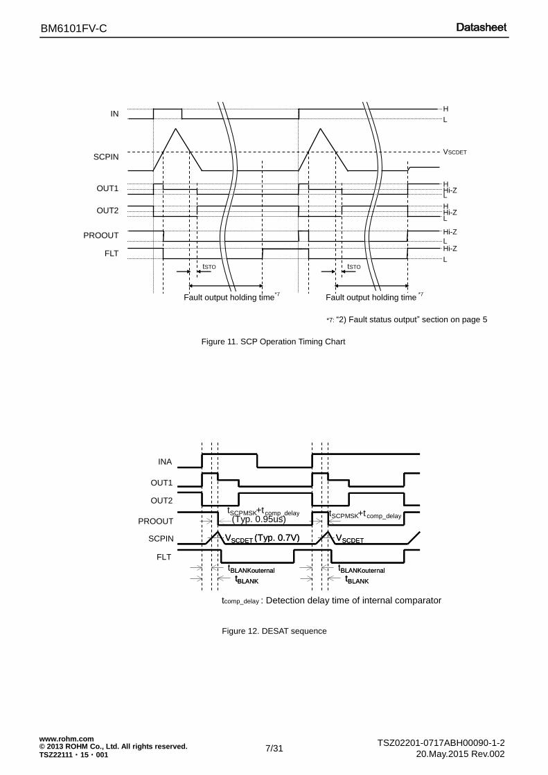
Figure 11. SCP Operation Timing Chart
*7: “2) Fault status output” section on page 5
Figure 12. DESAT sequence
V SCDET ( Typ . 0.7V) V SCDET
t BLANKouternal t BLANKouternal t BLANK t BLANK
INA
OUT1
OUT2
PROOUT
SCPIN
FLT
V SCDET ( Typ . 0.7V) V SCDET
t BLANKouternal t BLANKouternal t BLANK t BLANK
t SCPMSK +t comp_delay t SCPMSK +t comp_delay (Typ. 0.95us)
tcomp_delay : Detection delay time of internal comparator
8/31
BM6101FV-C
TSZ02201-0717ABH00090-1-2 © 2013 ROHM Co., Ltd. All rights reserved. 20.May.2015 Rev.002
www.rohm.com
TSZ22111・15・001
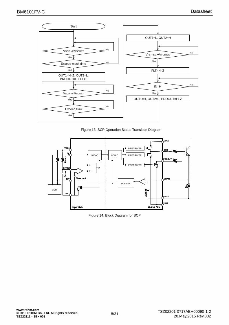
Figure 13. SCP Operation Status Transition Diagram
VSCPIN>VSCDET
Yes
No
Start
OUT1=Hi-Z, OUT2=L, PROOUT=L, FLT=L
OUT1=H, OUT2=L, PROOUT=Hi-Z
Exceed mask time
Yes
No
VFLTRLS>VTFLTRLS
Yes
No
IN=H
Yes
No
VSCPIN<VSCDET No
OUT1=L, OUT2=H
Yes
FLT=Hi-Z
Exceed tSTO No
Yes
Figure 14. Block Diagram for SCP
LOGIC
PREDRIVER
PREDRIVER
PREDRIVER
SCPMSK
-
+
LOGIC
-
+
ECU
VCC2
OUT
PROOUT
SCPIN
GND2
VEE2
VCC1
IN
FLTRLS
FLT
GND1
S
R
Input Side Output Side
VTFLTRLS
VS
CD
ET
RF
LT
RL
SC
FL
TR
LS
RS
CP
RSTO
LOGIC
PREDRIVER
PREDRIVER
PREDRIVER
SCPMSK
-
+
-
+
LOGIC
-
+
-
+
ECU
S
R
Input Side Output Side
VTFLTRLS
VS
CD
ET
RSTO
LOGIC
PREDRIVER
PREDRIVER
PREDRIVER
SCPMSK
-
+
-
+
LOGIC
-
+
-
+
ECU
VCC2
OUT
PROOUT
SCPIN
GND2
VEE2
VCC1
IN
FLTRLS
FLT
GND1
S
R
Input Side Output Side
VTFLTRLS
VS
CD
ET
RF
LT
RL
SC
FL
TR
LS
RS
CP
RSTO
LOGIC
PREDRIVER
PREDRIVER
PREDRIVER
SCPMSK
-
+
-
+
LOGIC
-
+
-
+
ECU
S
R
Input Side Output Side
VTFLTRLS
VS
CD
ET
RSTO
9/31
BM6101FV-C
TSZ02201-0717ABH00090-1-2 © 2013 ROHM Co., Ltd. All rights reserved. 20.May.2015 Rev.002
www.rohm.com
TSZ22111・15・001
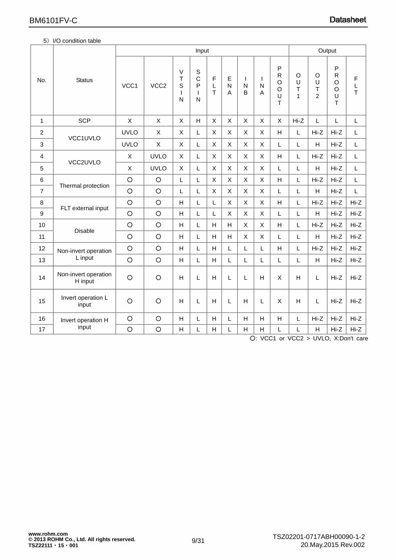
5)I/O condition table
No. Status
Input Output
VCC1 VCC2
V T S I N
S C P I N
F L T
E N A
I N B
I N A
P R O O U T
O U T 1
O U T 2
P R O O U T
F L T
1 SCP X X X H X X X X X Hi-Z L L L
2 VCC1UVLO
UVLO X X L X X X X H L Hi-Z Hi-Z L
3 UVLO X X L X X X X L L H Hi-Z L
4 VCC2UVLO
X UVLO X L X X X X H L Hi-Z Hi-Z L
5 X UVLO X L X X X X L L H Hi-Z L
6 Thermal protection
○ ○ L L X X X X H L Hi-Z Hi-Z L
7 ○ ○ L L X X X X L L H Hi-Z L
8 FLT external input
○ ○ H L L X X X H L Hi-Z Hi-Z Hi-Z
9 ○ ○ H L L X X X L L H Hi-Z Hi-Z
10 Disable
○ ○ H L H H X X H L Hi-Z Hi-Z Hi-Z
11 ○ ○ H L H H X X L L H Hi-Z Hi-Z
12 Non-invert operation L input
○ ○ H L H L L L H L Hi-Z Hi-Z Hi-Z
13 ○ ○ H L H L L L L L H Hi-Z Hi-Z
14 Non-invert operation
H input ○ ○ H L H L L H X H L Hi-Z Hi-Z
15 Invert operation L
input ○ ○ H L H L H L X H L Hi-Z Hi-Z
16 Invert operation H input
○ ○ H L H L H H H L Hi-Z Hi-Z Hi-Z
17 ○ ○ H L H L H H L L H Hi-Z Hi-Z
○: VCC1 or VCC2 > UVLO, X:Don't care
10/31
BM6101FV-C
TSZ02201-0717ABH00090-1-2 © 2013 ROHM Co., Ltd. All rights reserved. 20.May.2015 Rev.002
www.rohm.com
TSZ22111・15・001
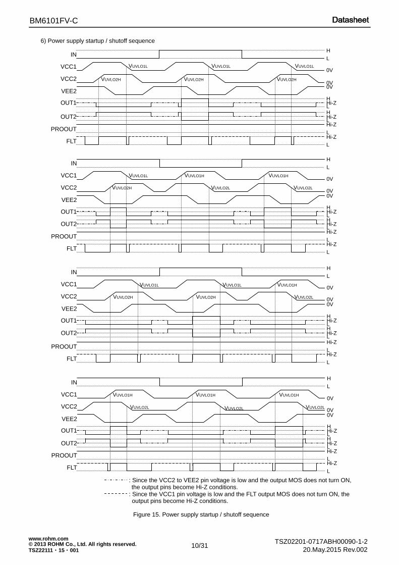
6) Power supply startup / shutoff sequence
OUT1
PROOUT
FLT
VCC1
VCC2
VEE2
IN H
L
H
L
Hi-Z
L Hi-Z
L
Hi-Z
VUVLO2L
VUVLO1H
VUVLO2L
VUVLO1H
VUVLO2L
VUVLO1H 0V
0V 0V
OUT2 L Hi-Z H
OUT1
PROOUT
FLT
VCC1
VCC2
VEE2
IN H
L
H
L
Hi-Z
L Hi-Z
L
Hi-Z
VUVLO2H
VUVLO1L
VUVLO2H
VUVLO1L
VUVLO2L
VUVLO1H 0V
0V 0V
OUT2 L Hi-Z H
OUT1
PROOUT
FLT
VCC1
VCC2
VEE2
IN H
L
H
L
Hi-Z
L Hi-Z
L
Hi-Z
VUVLO2H
VUVLO1L
VUVLO2L
VUVLO1H
VUVLO2L
VUVLO1H 0V
0V 0V
OUT2 L Hi-Z H
OUT1
PROOUT
FLT
VCC1
VCC2
VEE2
IN H
L
H
L
Hi-Z
L Hi-Z
L
Hi-Z
VUVLO2H
VUVLO1L
VUVLO2H
VUVLO1L
VUVLO2H
VUVLO1L 0V
0V 0V
OUT2 L Hi-Z H
: Since the VCC2 to VEE2 pin voltage is low and the output MOS does not turn ON, the output pins become Hi-Z conditions.
: Since the VCC1 pin voltage is low and the FLT output MOS does not turn ON, the output pins become Hi-Z conditions.
Figure 15. Power supply startup / shutoff sequence
11/31
BM6101FV-C
TSZ02201-0717ABH00090-1-2 © 2013 ROHM Co., Ltd. All rights reserved. 20.May.2015 Rev.002
www.rohm.com
TSZ22111・15・001
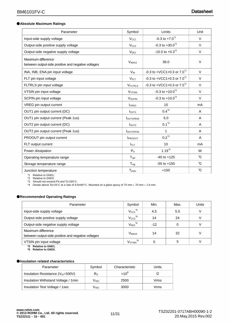
●Absolute Maximum Ratings
*1 Relative to GND1. *2 Relative to GND2.
*3 Should not exceed Pd and Tj=150C.
*4 Derate above Ta=25C at a rate of 9.5mW/C. Mounted on a glass epoxy of 70 mm 70 mm 1.6 mm.
●Recommended Operating Ratings
Parameter Symbol Min. Max. Units
Input-side supply voltage VCC1*5
4.5 5.5 V
Output-side positive supply voltage VCC2*6
14 24 V
Output-side negative supply voltage VEE2*6
-12 0 V
Maximum difference
between output-side positive and negative voltages VMAX2 14 32 V
VTSIN pin input voltage VVTSIN*6
0 5 V
*5 Relative to GND1. *6 Relative to GND2.
●Insulation related characteristics
Parameter Symbol Characteristic Units
Insulation Resistance (VIO=500V) RS >109 Ω
Insulation Withstand Voltage / 1min VISO 2500 Vrms
Insulation Test Voltage / 1sec VISO 3000 Vrms
Parameter Symbol Limits Unit
Input-side supply voltage VCC1 -0.3 to +7.0*1
V
Output-side positive supply voltage VCC2 -0.3 to +30.0*2
V
Output-side negative supply voltage VEE2 -15.0 to +0.3*2
V
Maximum difference
between output-side positive and negative voltages VMAX2 36.0 V
INA, INB, ENA pin input voltage VIN -0.3 to +VCC1+0.3 or 7.0*1
V
FLT pin input voltage VFLT -0.3 to +VCC1+0.3 or 7.0*1
V
FLTRLS pin input voltage VFLTRLS -0.3 to +VCC1+0.3 or 7.0*1
V
VTSIN pin input voltage VVTSIN -0.3 to +10.0*2
V
SCPIN pin input voltage VSCPIN -0.3 to +10.0*2
V
VREG pin output current IVREG 10 mA
OUT1 pin output current (DC) IOUT1 0.4*3
A
OUT1 pin output current (Peak 1us) IOUT1PEAK 5.0 A
OUT2 pin output current (DC) IOUT2 0.1*3
A
OUT2 pin output current (Peak 1us) IOUT2PEAK 1 A
PROOUT pin output current IPROOUT 0.2*3
A
FLT output current IFLT 10 mA
Power dissipation Pd 1.19*4
W
Operating temperature range Topr -40 to +125 ℃
Storage temperature range Tstg -55 to +150 ℃
Junction temperature Tjmax +150 ℃
12/31
BM6101FV-C
TSZ02201-0717ABH00090-1-2 © 2013 ROHM Co., Ltd. All rights reserved. 20.May.2015 Rev.002
www.rohm.com
TSZ22111・15・001
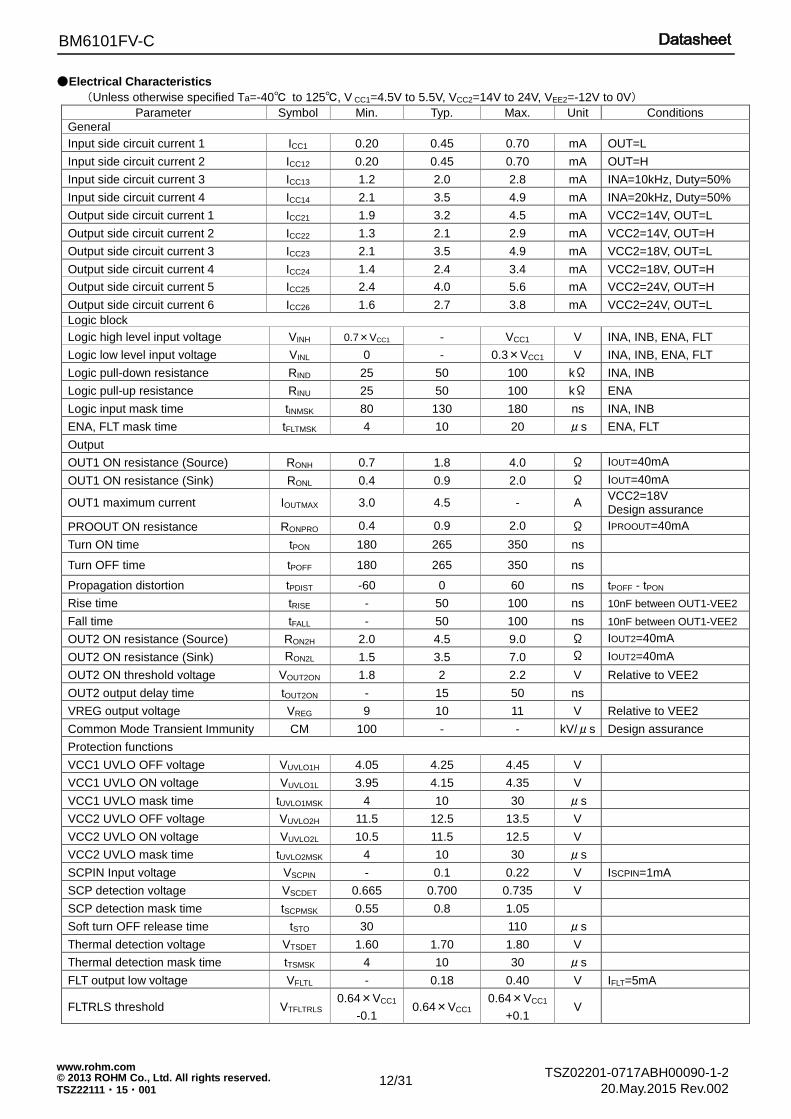
●Electrical Characteristics
(Unless otherwise specified Ta=-40℃ to 125℃, V CC1=4.5V to 5.5V, VCC2=14V to 24V, VEE2=-12V to 0V)
Parameter Symbol Min. Typ. Max. Unit Conditions
General
Input side circuit current 1 ICC1 0.20 0.45 0.70 mA OUT=L
Input side circuit current 2 ICC12 0.20 0.45 0.70 mA OUT=H
Input side circuit current 3 ICC13 1.2 2.0 2.8 mA INA=10kHz, Duty=50%
Input side circuit current 4 ICC14 2.1 3.5 4.9 mA INA=20kHz, Duty=50%
Output side circuit current 1 ICC21 1.9 3.2 4.5 mA VCC2=14V, OUT=L
Output side circuit current 2 ICC22 1.3 2.1 2.9 mA VCC2=14V, OUT=H
Output side circuit current 3 ICC23 2.1 3.5 4.9 mA VCC2=18V, OUT=L
Output side circuit current 4 ICC24 1.4 2.4 3.4 mA VCC2=18V, OUT=H
Output side circuit current 5 ICC25 2.4 4.0 5.6 mA VCC2=24V, OUT=H
Output side circuit current 6 ICC26 1.6 2.7 3.8 mA VCC2=24V, OUT=L
Logic block
Logic high level input voltage VINH 0.7×VCC1 - VCC1 V INA, INB, ENA, FLT
Logic low level input voltage VINL 0 - 0.3×VCC1 V INA, INB, ENA, FLT
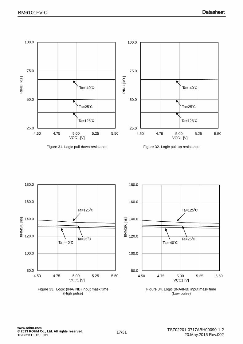
Logic pull-down resistance RIND 25 50 100 kΩ INA, INB
Logic pull-up resistance RINU 25 50 100 kΩ ENA
Logic input mask time tINMSK 80 130 180 ns INA, INB
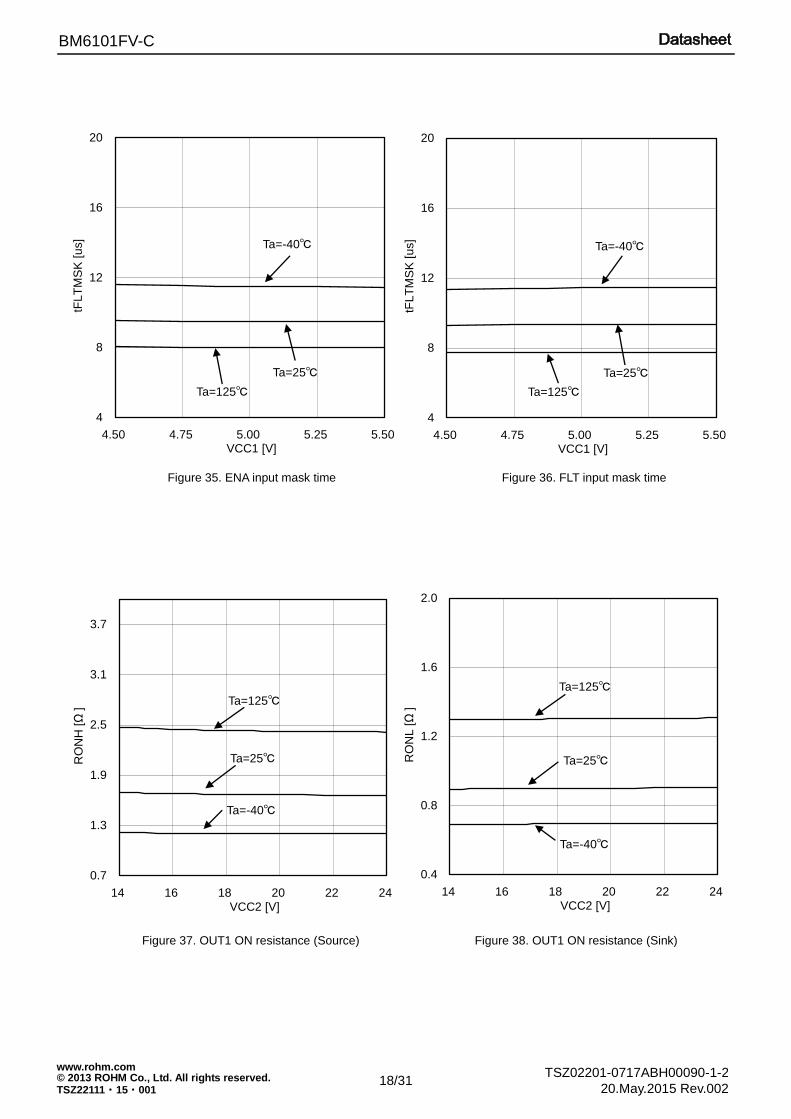
ENA, FLT mask time tFLTMSK 4 10 20 μs ENA, FLT
Output
OUT1 ON resistance (Source) RONH 0.7 1.8 4.0 Ω IOUT=40mA
OUT1 ON resistance (Sink) RONL 0.4 0.9 2.0 Ω IOUT=40mA
OUT1 maximum current IOUTMAX 3.0 4.5 - A VCC2=18V Design assurance
PROOUT ON resistance RONPRO 0.4 0.9 2.0 Ω IPROOUT=40mA
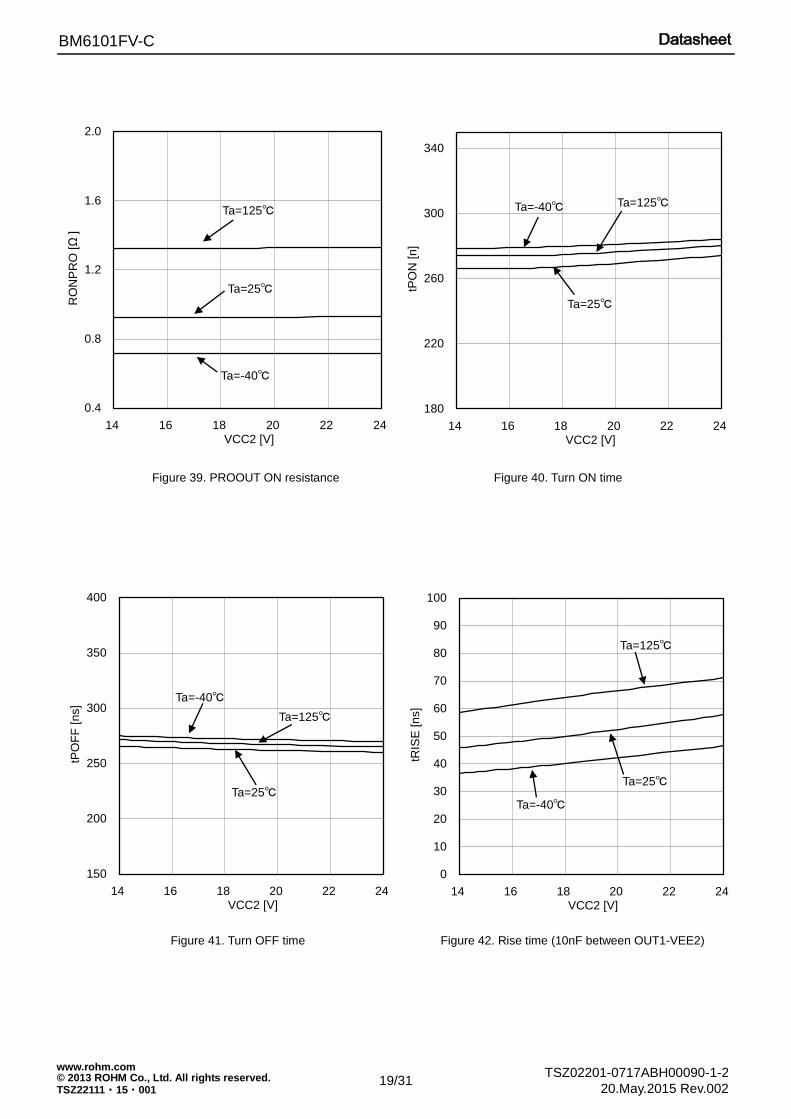
Turn ON time tPON 180 265 350 ns
Turn OFF time tPOFF 180 265 350 ns
Propagation distortion tPDIST -60 0 60 ns tPOFF - tPON
Rise time tRISE - 50 100 ns 10nF between OUT1-VEE2
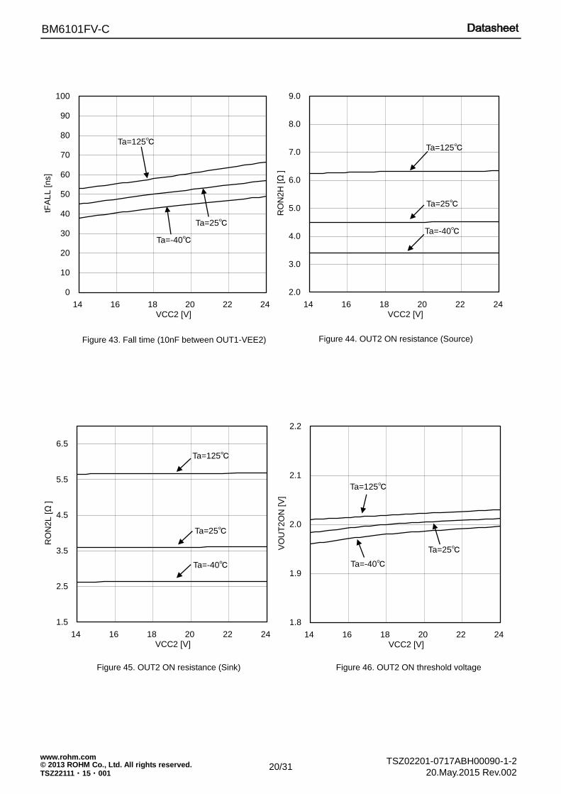
Fall time tFALL - 50 100 ns 10nF between OUT1-VEE2
OUT2 ON resistance (Source) RON2H 2.0 4.5 9.0 Ω IOUT2=40mA
OUT2 ON resistance (Sink) RON2L 1.5 3.5 7.0 Ω IOUT2=40mA
OUT2 ON threshold voltage VOUT2ON 1.8 2 2.2 V Relative to VEE2
OUT2 output delay time tOUT2ON - 15 50 ns
VREG output voltage VREG 9 10 11 V Relative to VEE2
Common Mode Transient Immunity CM 100 - - kV/μs Design assurance
Protection functions
VCC1 UVLO OFF voltage VUVLO1H 4.05 4.25 4.45 V
VCC1 UVLO ON voltage VUVLO1L 3.95 4.15 4.35 V
VCC1 UVLO mask time tUVLO1MSK 4 10 30 μs
VCC2 UVLO OFF voltage VUVLO2H 11.5 12.5 13.5 V
VCC2 UVLO ON voltage VUVLO2L 10.5 11.5 12.5 V
VCC2 UVLO mask time tUVLO2MSK 4 10 30 μs
SCPIN Input voltage VSCPIN - 0.1 0.22 V ISCPIN=1mA
SCP detection voltage VSCDET 0.665 0.700 0.735 V
SCP detection mask time tSCPMSK 0.55 0.8 1.05
Soft turn OFF release time tSTO 30 110 μs
Thermal detection voltage VTSDET 1.60 1.70 1.80 V
Thermal detection mask time tTSMSK 4 10 30 μs
FLT output low voltage VFLTL - 0.18 0.40 V IFLT=5mA
FLTRLS threshold VTFLTRLS 0.64×VCC1
-0.1 0.64×VCC1
0.64×VCC1
+0.1 V
13/31
BM6101FV-C
TSZ02201-0717ABH00090-1-2 © 2013 ROHM Co., Ltd. All rights reserved. 20.May.2015 Rev.002
www.rohm.com
TSZ22111・15・001
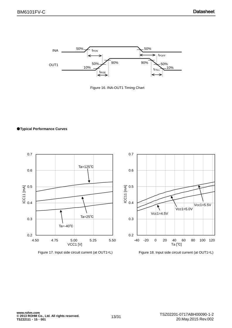
●Typical Performance Curves
INA
OUT1
tRISE tFALL
tPON
tPOFF
50% 50%
90% 50% 50% 90%
10% 10%
Figure 16. INA-OUT1 Timing Chart
0.2
0.3
0.4
0.5
0.6
0.7
4.50 4.75 5.00 5.25 5.50
VCC1 [V]
ICC
11
[m
A]
0.2
0.3
0.4
0.5
0.6
0.7
-40 -20 0 20 40 60 80 100 120
Ta [℃]
ICC
11
[m
A]
Figure 17. Input side circuit current (at OUT1=L) Figure 18. Input side circuit current (at OUT1=L)
Ta=125℃
Ta=25℃
Ta=-40℃
Vcc1=5.5V Vcc1=5.0V
Vcc1=4.5V
14/31
BM6101FV-C
TSZ02201-0717ABH00090-1-2 © 2013 ROHM Co., Ltd. All rights reserved. 20.May.2015 Rev.002
www.rohm.com
TSZ22111・15・001
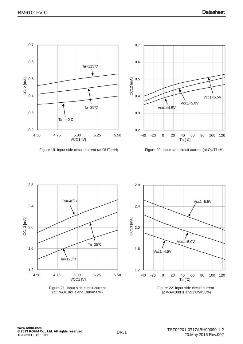
Figure 19. Input side circuit current (at OUT1=H) Figure 20. Input side circuit current (at OUT1=H)
Figure 21. Input side circuit current (at INA=10kHz and Duty=50%)
Figure 22. Input side circuit current (at INA=10kHz and Duty=50%)
0.2
0.3
0.4
0.5
0.6
0.7
4.50 4.75 5.00 5.25 5.50
VCC1 [V]
ICC
12
[m
A]
Ta=125℃
Ta=25℃
Ta=-40℃
0.2
0.3
0.4
0.5
0.6
0.7
-40 -20 0 20 40 60 80 100 120
Ta [℃]
ICC
12
[m
A]
Vcc1=5.5V
Vcc1=5.0V
Vcc1=4.5V
1.2
1.6
2.0
2.4
2.8
4.50 4.75 5.00 5.25 5.50
VCC1 [V]
ICC
13
[m
A]
1.2
1.6
2.0
2.4
2.8
-40 -20 0 20 40 60 80 100 120
Ta [℃]
ICC
13
[m
A]
Vcc1=5.5V
Vcc1=5.0V
Vcc1=4.5V
Ta=125℃
Ta=25℃
Ta=-40℃
15/31
BM6101FV-C
TSZ02201-0717ABH00090-1-2 © 2013 ROHM Co., Ltd. All rights reserved. 20.May.2015 Rev.002
www.rohm.com
TSZ22111・15・001
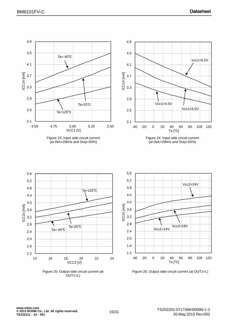
Figure 23. Input side circuit current (at INA=20kHz and Duty=50%)
Figure 24. Input side circuit current (at INA=20kHz and Duty=50%)
Figure 25. Output side circuit current (at OUT1=L)
Figure 26. Output side circuit current (at OUT1=L)
2.1
2.5
2.9
3.3
3.7
4.1
4.5
4.9
4.50 4.75 5.00 5.25 5.50
VCC1 [V]
ICC
14
[m
A]
2.1
2.5
2.9
3.3
3.7
4.1
4.5
4.9
-40 -20 0 20 40 60 80 100 120
Ta [℃]
ICC
14
[m
A]
1.2
1.6
2.0
2.4
2.8
3.2
3.6
4.0
4.4
4.8
5.2
5.6
14 16 18 20 22 24
VCC2 [V]
ICC
2x [
mA
]
1.2
1.6
2.0
2.4
2.8
3.2
3.6
4.0
4.4
4.8
5.2
5.6
-40 -20 0 20 40 60 80 100 120
Ta [℃]
ICC
2x [
mA
]
Ta=125℃
Ta=25℃ Ta=-40℃
Vcc2=24V
Vcc2=18V Vcc2=14V
Ta=125℃
Ta=25℃
Ta=-40℃ Vcc1=5.5V
Vcc1=5.0V
Vcc1=4.5V
16/31
BM6101FV-C
TSZ02201-0717ABH00090-1-2 © 2013 ROHM Co., Ltd. All rights reserved. 20.May.2015 Rev.002
www.rohm.com
TSZ22111・15・001
Figure 29. Logic (INA/INB/ENA) High/Low level input voltage
Figure 30. Logic (INA/INB/ENA) High/Low level
input voltage at Ta=25℃
Figure 27. Output side circuit current (at OUT1=H)
Figure 28. Output side circuit current (at OUT1=H)
0.0
0.5
1.0
1.5
2.0
2.5
3.0
3.5
4.0
4.5
5.0
4.50 4.75 5.00 5.25 5.50
VCC1 [V]
VIN
H / V
INL
[V
]
H level
Ta=125℃
Ta=25℃
Ta=-40℃
Ta=-40℃
Ta=25℃
Ta=125℃
L level
1.2
1.6
2.0
2.4
2.8
3.2
3.6
4.0
4.4
4.8
5.2
5.6
14 16 18 20 22 24VCC2 [V]
ICC
2x [
mA
]
Ta=125℃
Ta=25℃
Ta=-40℃ 1.2
1.6
2.0
2.4
2.8
3.2
3.6
4.0
4.4
4.8
5.2
5.6
-40 -20 0 20 40 60 80 100 120
Ta [℃]
ICC
2x [
mA
]
Vcc2=24V
Vcc2=18V
Vcc2=14V
0
4
8
12
16
20
24
0 1 2 3 4 5INA [V]
OU
T1
[V
]
Vcc1=5V
17/31
BM6101FV-C
TSZ02201-0717ABH00090-1-2 © 2013 ROHM Co., Ltd. All rights reserved. 20.May.2015 Rev.002
www.rohm.com
TSZ22111・15・001
Figure 31. Logic pull-down resistance Figure 32. Logic pull-up resistance
Figure 33. Logic (INA/INB) input mask time (High pulse)
Figure 34. Logic (INA/INB) input mask time (Low pulse)
25.0
50.0
75.0
100.0
4.50 4.75 5.00 5.25 5.50VCC1 [V]
RIN
U [
kΩ
]
25.0
50.0
75.0
100.0
4.50 4.75 5.00 5.25 5.50VCC1 [V]
RIN
D [
kΩ
]
Ta=125℃
80.0
100.0
120.0
140.0
160.0
180.0
4.50 4.75 5.00 5.25 5.50VCC1 [V]
tIN
MS
K [
ns]
Ta=-40℃ Ta=25℃
Ta=125℃
80.0
100.0
120.0
140.0
160.0
180.0
4.50 4.75 5.00 5.25 5.50VCC1 [V]
tIN
MS
K [
ns]
Ta=-40℃
Ta=25℃
Ta=-40℃ Ta=25℃
Ta=125℃
Ta=125℃
Ta=-40℃
Ta=25℃
18/31
BM6101FV-C
TSZ02201-0717ABH00090-1-2 © 2013 ROHM Co., Ltd. All rights reserved. 20.May.2015 Rev.002
www.rohm.com
TSZ22111・15・001
Figure 35. ENA input mask time Figure 36. FLT input mask time
Figure 37. OUT1 ON resistance (Source) Figure 38. OUT1 ON resistance (Sink)
4
8
12
16
20
4.50 4.75 5.00 5.25 5.50VCC1 [V]
tFL
TM
SK
[u
s]
Ta=-40℃
Ta=25℃
Ta=125℃
4
8
12
16
20
4.50 4.75 5.00 5.25 5.50VCC1 [V]
tFL
TM
SK
[u
s]
Ta=-40℃
Ta=25℃
Ta=125℃
0.7
1.3
1.9
2.5
3.1
3.7
14 16 18 20 22 24
VCC2 [V]
RO
NH
[Ω
]
Ta=-40℃
Ta=25℃
Ta=125℃
0.4
0.8
1.2
1.6
2.0
14 16 18 20 22 24
VCC2 [V]
RO
NL [Ω
]
Ta=125℃
Ta=25℃
Ta=-40℃
19/31
BM6101FV-C
TSZ02201-0717ABH00090-1-2 © 2013 ROHM Co., Ltd. All rights reserved. 20.May.2015 Rev.002
www.rohm.com
TSZ22111・15・001
Figure 39. PROOUT ON resistance Figure 40. Turn ON time
Figure 41. Turn OFF time Figure 42. Rise time (10nF between OUT1-VEE2)
0.4
0.8
1.2
1.6
2.0
14 16 18 20 22 24
VCC2 [V]
RO
NP
RO
[Ω
]
Ta=125℃
Ta=25℃
Ta=-40℃
180
220
260
300
340
14 16 18 20 22 24
VCC2 [V]
tPO
N [n
]
150
200
250
300
350
400
14 16 18 20 22 24
VCC2 [V]
tPO
FF
[n
s]
Ta=25℃
Ta=-40℃ Ta=125℃
Ta=25℃
Ta=-40℃
Ta=125℃
0
10
20
30
40
50
60
70
80
90
100
14 16 18 20 22 24
VCC2 [V]
tRIS
E [
ns]
Ta=25℃
Ta=-40℃
Ta=125℃
20/31
BM6101FV-C
TSZ02201-0717ABH00090-1-2 © 2013 ROHM Co., Ltd. All rights reserved. 20.May.2015 Rev.002
www.rohm.com
TSZ22111・15・001
Figure 43. Fall time (10nF between OUT1-VEE2) Figure 44. OUT2 ON resistance (Source)
Figure 45. OUT2 ON resistance (Sink) Figure 46. OUT2 ON threshold voltage
2.0
3.0
4.0
5.0
6.0
7.0
8.0
9.0
14 16 18 20 22 24
VCC2 [V]
RO
N2H
[Ω
]
1.5
2.5
3.5
4.5
5.5
6.5
14 16 18 20 22 24
VCC2 [V]
RO
N2L
[Ω
]
Ta=25℃
Ta=125℃
Ta=-40℃
Ta=25℃
Ta=125℃
Ta=-40℃
1.8
1.9
2.0
2.1
2.2
14 16 18 20 22 24
VCC2 [V]
VO
UT
2O
N [V
]
Ta=125℃
Ta=-40℃
Ta=25℃
0
10
20
30
40
50
60
70
80
90
100
14 16 18 20 22 24
VCC2 [V]
tFA
LL
[n
s]
Ta=125℃
Ta=25℃
Ta=-40℃
21/31
BM6101FV-C
TSZ02201-0717ABH00090-1-2 © 2013 ROHM Co., Ltd. All rights reserved. 20.May.2015 Rev.002
www.rohm.com
TSZ22111・15・001
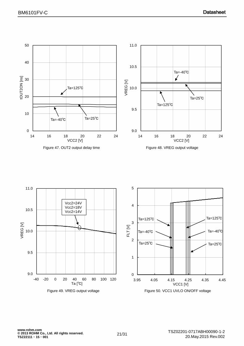
Figure 47. OUT2 output delay time Figure 48. VREG output voltage
Figure 49. VREG output voltage Figure 50. VCC1 UVLO ON/OFF voltage
0
10
20
30
40
50
14 16 18 20 22 24
VCC2 [V]
tOU
T2
ON
[n
s]
Ta=125℃
Ta=25℃ Ta=-40℃
9.0
9.5
10.0
10.5
11.0
14 16 18 20 22 24
VCC2 [V]
VR
EG
[V
]
Ta=-40℃
Ta=25℃
Ta=125℃
9.0
9.5
10.0
10.5
11.0
-40 -20 0 20 40 60 80 100 120
Ta [℃]
VR
EG
[V
]
Vcc2=24V Vcc2=18V Vcc2=14V
0
1
2
3
4
5
3.95 4.05 4.15 4.25 4.35 4.45VCC1 [V]
FL
T [
V]
Ta=125℃
Ta=-40℃
Ta=25℃ Ta=25℃
Ta=-40℃
Ta=125℃
22/31
BM6101FV-C
TSZ02201-0717ABH00090-1-2 © 2013 ROHM Co., Ltd. All rights reserved. 20.May.2015 Rev.002
www.rohm.com
TSZ22111・15・001
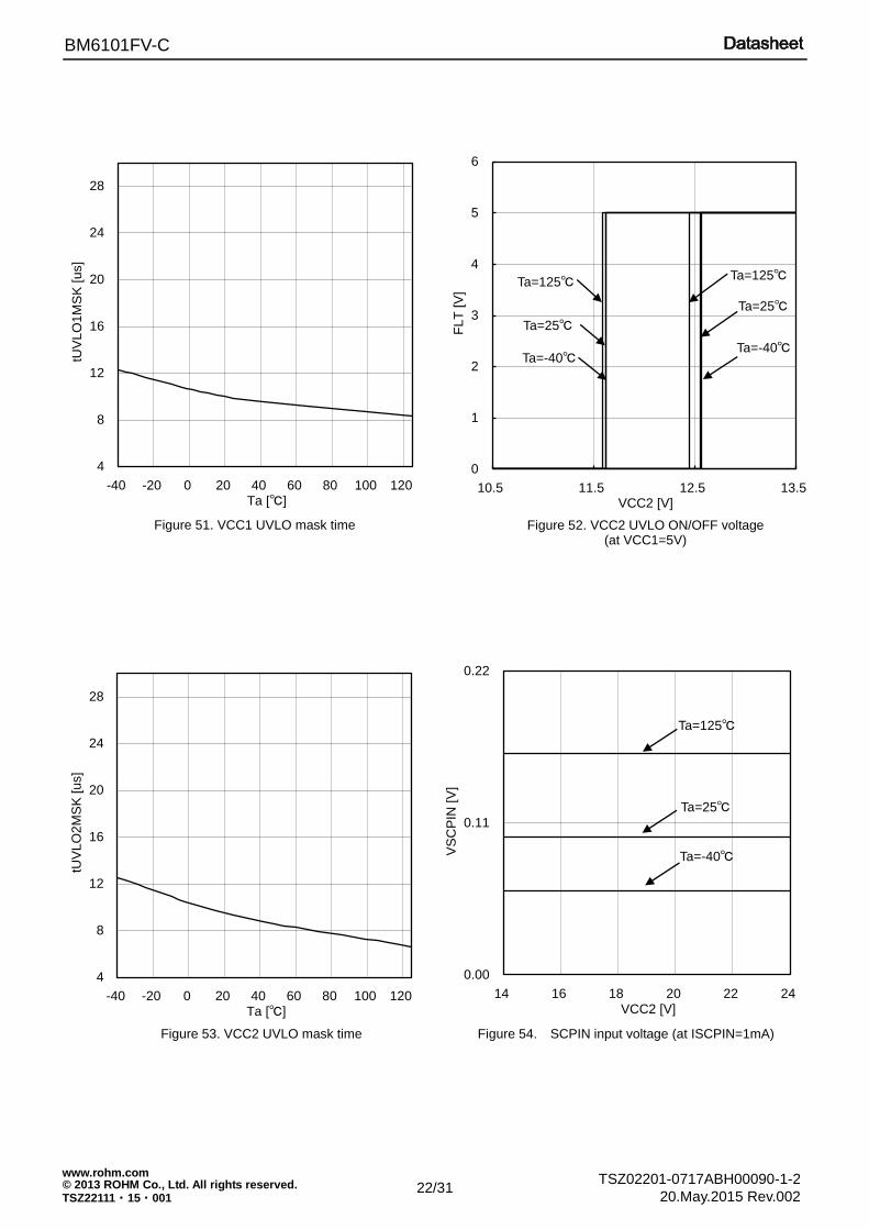
Figure 51. VCC1 UVLO mask time Figure 52. VCC2 UVLO ON/OFF voltage (at VCC1=5V)
Figure 53. VCC2 UVLO mask time Figure 54. SCPIN input voltage (at ISCPIN=1mA)
0.00
0.11
0.22
14 16 18 20 22 24
VCC2 [V]
VS
CP
IN [
V]
4
8
12
16
20
24
28
-40 -20 0 20 40 60 80 100 120
Ta [℃]
tUV
LO
1M
SK
[u
s]
0
1
2
3
4
5
6
10.5 11.5 12.5 13.5VCC2 [V]
FL
T [
V]
Ta=125℃
Ta=25℃
Ta=-40℃ Ta=-40℃
Ta=25℃
Ta=125℃
4
8
12
16
20
24
28
-40 -20 0 20 40 60 80 100 120
Ta [℃]
tUV
LO
2M
SK
[u
s]
Ta=-40℃
Ta=25℃
Ta=125℃
23/31
BM6101FV-C
TSZ02201-0717ABH00090-1-2 © 2013 ROHM Co., Ltd. All rights reserved. 20.May.2015 Rev.002
www.rohm.com
TSZ22111・15・001
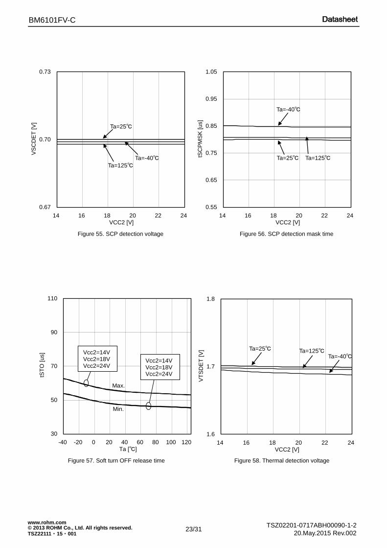
Figure 55. SCP detection voltage Figure 56. SCP detection mask time
Figure 57. Soft turn OFF release time Figure 58. Thermal detection voltage
0.67
0.70
0.73
14 16 18 20 22 24
VCC2 [V]
VS
CD
ET
[V
]
Ta=25℃
Ta=-40℃
Ta=125℃
0.55
0.65
0.75
0.85
0.95
1.05
14 16 18 20 22 24
VCC2 [V]
tSC
PM
SK
[u
s]
1.6
1.7
1.8
14 16 18 20 22 24
VCC2 [V]
VT
SD
ET
[V
]
Ta=-40℃
Ta=125℃ Ta=25℃
30
50
70
90
110
-40 -20 0 20 40 60 80 100 120
Ta [℃]
tST
O [
us]
Vcc2=14V Vcc2=18V Vcc2=24V
Max.
Min.
Vcc2=14V Vcc2=18V Vcc2=24V
Ta=25℃ Ta=125℃ Ta=-40℃
24/31
BM6101FV-C
TSZ02201-0717ABH00090-1-2 © 2013 ROHM Co., Ltd. All rights reserved. 20.May.2015 Rev.002
www.rohm.com
TSZ22111・15・001
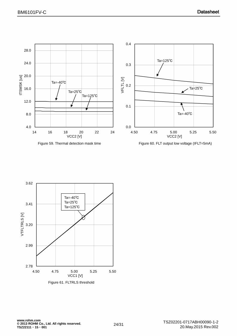
Figure 59. Thermal detection mask time Figure 60. FLT output low voltage (IFLT=5mA)
Figure 61. FLTRLS threshold
4.0
8.0
12.0
16.0
20.0
24.0
28.0
14 16 18 20 22 24
VCC2 [V]
tTS
MS
K [
us]
Ta=125℃ Ta=25℃
Ta=-40℃
0.0
0.1
0.2
0.3
0.4
4.50 4.75 5.00 5.25 5.50
VCC2 [V]
VF
LT
L [
V]
2.78
2.99
3.20
3.41
3.62
4.50 4.75 5.00 5.25 5.50
VCC1 [V]
VT
FL
TR
LS
[V
]
Ta=-40℃
Ta=125℃
Ta=25℃
Ta=-40℃
Ta=25℃
Ta=125℃
25/31
BM6101FV-C
TSZ02201-0717ABH00090-1-2 © 2013 ROHM Co., Ltd. All rights reserved. 20.May.2015 Rev.002
www.rohm.com
TSZ22111・15・001
●Selection of Components Externally Connected
R F
LT
RL
S
C FL
TR
LS
OUT1
VTSIN
Input side chip
NC
GND1
GND1
INA
TIMER
TIMER
UVLO
FLTRLS
VCC1
Output side chip
TEST VEE2
MASK
VREG
OUT2
FLT
VCC2
LOGIC
S
R
Q
PROOUT
VEE2 PRE DRIVER
MASK
MASK
MASK FB
C V
CC
1
C V
CC
2
FLT
ENA
ECU
INB
GND2
MASK
LOGIC
MASK
FLT
Temp Sensor
UVLO
SCPIN
VEE2
R FL
TR
LS
C FL
TR
LS
OUT1
VTSIN
Input side chip
NC
GND1
GND1
INA
TIMER
TIMER
UVLO
FLTRLS
VCC1
Output side chip
TEST VEE2
MASK
VREG
OUT2
FLT
VCC2
LOGIC
S
R
Q
PROOUT
VEE2 PRE DRIVER
MASK
MASK
MASK FB
C V
CC
1
C VC
C2
FLT
ENA
ECU
INB
GND2
MASK
LOGIC
MASK
FLT
Temp Sensor
UVLO
SCPIN
VEE2
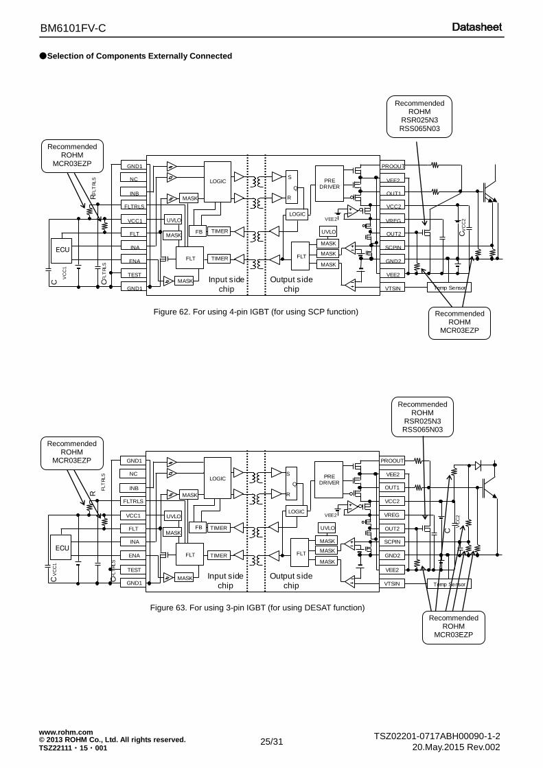
Figure 62. For using 4-pin IGBT (for using SCP function)
Figure 63. For using 3-pin IGBT (for using DESAT function)
Recommended ROHM
MCR03EZP
Recommended ROHM
MCR03EZP
Recommended ROHM
MCR03EZP
Recommended ROHM
RSR025N3 RSS065N03
Recommended ROHM
RSR025N3 RSS065N03
Recommended ROHM
MCR03EZP
26/31
BM6101FV-C
TSZ02201-0717ABH00090-1-2 © 2013 ROHM Co., Ltd. All rights reserved. 20.May.2015 Rev.002
www.rohm.com
TSZ22111・15・001
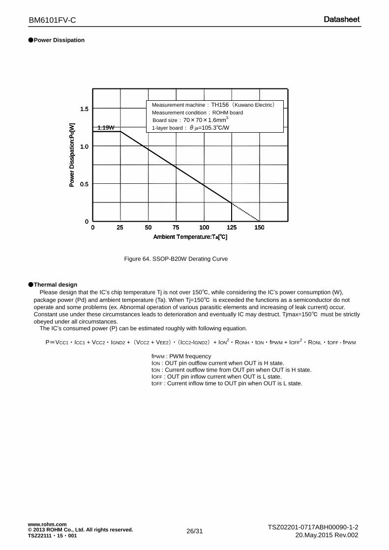
●Power Dissipation
●Thermal design
Please design that the IC’s chip temperature Tj is not over 150℃, while considering the IC’s power consumption (W),
package power (Pd) and ambient temperature (Ta). When Tj=150℃ is exceeded the functions as a semiconductor do not
operate and some problems (ex. Abnormal operation of various parasitic elements and increasing of leak current) occur.
Constant use under these circumstances leads to deterioration and eventually IC may destruct. Tjmax=150℃ must be strictly
obeyed under all circumstances. The IC’s consumed power (P) can be estimated roughly with following equation.
P=VCC1・ICC1 + VCC2・IGND2 +(VCC2 + VEE2)・(ICC2-IGND2)+ ION2・RONH・tON・fPWM + IOFF
2・RONL・tOFF・fPWM
fPWM : PWM frequency ION : OUT pin outflow current when OUT is H state. tON : Current outflow time from OUT pin when OUT is H state. IOFF : OUT pin inflow current when OUT is L state. tOFF : Current inflow time to OUT pin when OUT is L state.
0 25 50 75 100 125 1500
0.5
1.0
1.5
Ambient Temperature:Ta[℃]
Po
we
r D
issip
atio
n:P
d[W
]
1.19W
0 25 50 75 100 125 1500
0.5
1.0
1.5
Ambient Temperature:Ta[℃]
Po
we
r D
issip
atio
n:P
d[W
]
0 25 50 75 100 125 1500
0.5
1.0
1.5
Ambient Temperature:Ta[℃]
Po
we
r D
issip
atio
n:P
d[W
]
0 25 50 75 100 125 1500
0.5
1.0
1.5
Ambient Temperature:Ta[℃]
Po
we
r D
issip
atio
n:P
d[W
]
1.19W
Measurement machine:TH156(Kuwano Electric)
Measurement condition:ROHM board
Board size:70×70×1.6mm3
1-layer board:θja=105.3℃/W
Figure 64. SSOP-B20W Derating Curve
27/31
BM6101FV-C
TSZ02201-0717ABH00090-1-2 © 2013 ROHM Co., Ltd. All rights reserved. 20.May.2015 Rev.002
www.rohm.com
TSZ22111・15・001
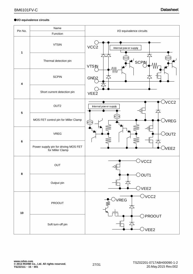
●I/O equivalence circuits
Pin No. Name
I/O equivalence circuits Function
1
VTSIN VCC2
SCPIN
VEE2
GND2
VTSIN
Internal pow er supply
Thermal detection pin
4
SCPIN
Short current detection pin
5
OUT2
VEE2
VCC2
OUT2
VREG
Internal pow er supply
MOS FET control pin for Miller Clamp
6
VREG
Power supply pin for driving MOS FET for Miller Clamp
8
OUT
OUT1
VEE2
VCC2
Output pin
10
PROOUT
PROOUT
VEE2
VCC2 VREG
Soft turn-off pin
28/31
BM6101FV-C
TSZ02201-0717ABH00090-1-2 © 2013 ROHM Co., Ltd. All rights reserved. 20.May.2015 Rev.002
www.rohm.com
TSZ22111・15・001
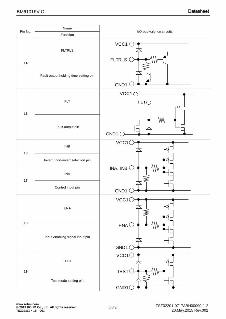
Pin No. Name
I/O equivalence circuits Function
14
FLTRLS
FLTRLS
GND1
VCC1
Fault output holding time setting pin
16
FLT FLT
GND1
VCC1
Fault output pin
13
INB
INA, INB
GND1
VCC1
Invert / non-invert selection pin
17
INA
Control input pin
18
ENA
ENA
GND1
VCC1
Input enabling signal input pin
19
TEST
TEST
GND1
VCC1
Test mode setting pin
29/31
BM6101FV-C
TSZ02201-0717ABH00090-1-2 © 2013 ROHM Co., Ltd. All rights reserved. 20.May.2015 Rev.002
www.rohm.com
TSZ22111・15・001
●Operational Notes
(1) Absolute maximum ratings An excess in the absolute maximum ratings, such as supply voltage, temperature range of operating conditions, etc., can break down the devices, thus making impossible to identify breaking mode, such as a short circuit or an open circuit. If any over rated values will expect to exceed the absolute maximum ratings, consider adding circuit protection devices, such as fuses.
(2) Connecting the power supply connector backward Connecting of the power supply in reverse polarity can damage IC. Take precautions when connecting the power supply lines. An external direction diode can be added.
(3) Power supply Lines Design PCB layout pattern to provide low impedance GND and supply lines. To obtain a low noise ground and supply line, separate the ground section and supply lines of the digital and analog blocks. Furthermore, for all power supply terminals to ICs, connect a capacitor between the power supply and the GND terminal. When applying electrolytic capacitors in the circuit, not that capacitance characteristic values are reduced at low temperatures.
(4) GND1 Potential The potential of GND1 pin must be minimum potential in all operating conditions. (Input side ; 11pin to 20pin)
(5) VEE2 Potential The potential of VEE2 pin must be minimum potential in all operating conditions. (Output side ; 1pin to 10pin)
(6) Thermal design Use a thermal design that allows for a sufficient margin in light of the power dissipation (Pd) in actual operating conditions.
(7) Inter-pin shorts and mounting errors When attaching to a printed circuit board, pay close attention to the direction of the IC and displacement. Improper attachment may lead to destruction of the IC. There is also possibility of destruction from short circuits which can be caused by foreign matter entering between outputs or an output and the power supply or GND.
(8) Operation in a strong electric field Use caution when using the IC in the presence of a strong electromagnetic field as doing so may cause the IC to malfunction.
(9) Inspection of the application board During inspection of the application board, if a capacitor is connected to a pin with low impedance there is a possibility that it could cause stress to the IC, therefore an electrical discharge should be performed after each process. Also, as a measure again electrostatic discharge, it should be earthed during the assembly process and special care should be taken during transport or storage. Furthermore, when connecting to the jig during the inspection process, the power supply should first be turned off and then removed before the inspection.
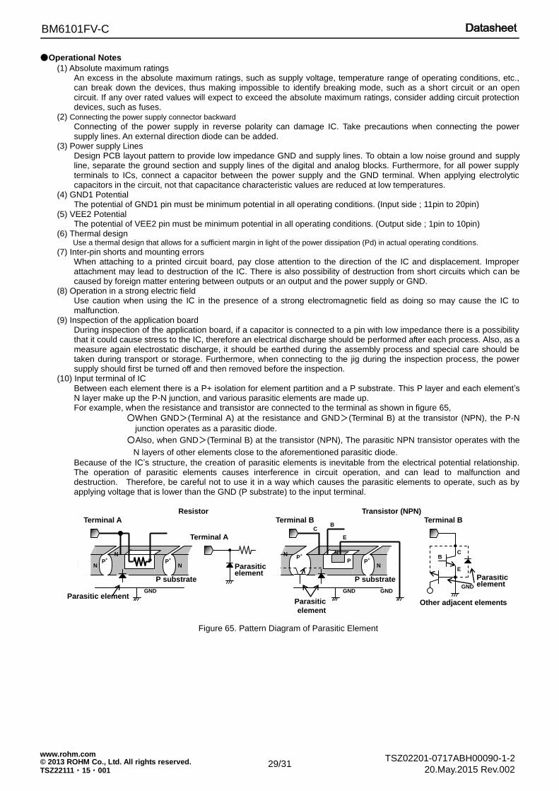
(10) Input terminal of IC Between each element there is a P+ isolation for element partition and a P substrate. This P layer and each element’s N layer make up the P-N junction, and various parasitic elements are made up. For example, when the resistance and transistor are connected to the terminal as shown in figure 65,
○When GND>(Terminal A) at the resistance and GND>(Terminal B) at the transistor (NPN), the P-N
junction operates as a parasitic diode.
○Also, when GND>(Terminal B) at the transistor (NPN), The parasitic NPN transistor operates with the
N layers of other elements close to the aforementioned parasitic diode.
Because of the IC’s structure, the creation of parasitic elements is inevitable from the electrical potential relationship. The operation of parasitic elements causes interference in circuit operation, and can lead to malfunction and destruction. Therefore, be careful not to use it in a way which causes the parasitic elements to operate, such as by applying voltage that is lower than the GND (P substrate) to the input terminal.
Figure 65. Pattern Diagram of Parasitic Element
Resistor Transistor (NPN)
N
N N P
+ P
+ P
P substrate
GND Parasitic element
Terminal A
N
N P
+
P+ P
P substrate
GND
Parasitic
element
Terminal B C
B
E
N
GND
Terminal A
Terminal B
Other adjacent elements
E
B C
GND
Parasitic element
Parasitic element
30/31
BM6101FV-C
TSZ02201-0717ABH00090-1-2 © 2013 ROHM Co., Ltd. All rights reserved. 20.May.2015 Rev.002
www.rohm.com
TSZ22111・15・001
(11) Ground Wiring Patterns When using both small signal and large current GND patterns, it is recommended to isolate the two ground patterns, placing a single ground point at the application's reference point so that the pattern wiring resistance and voltage variations caused by large currents do not cause variations in the small signal ground voltage. Be careful not to change the GND wiring pattern potential of any external components, either.
●Ordering Information
B M 6 1 0 1 F V - CE 2
Part Number Package
FV:SSOP-B20W Product class C : for Automotive applications Packaging and forming specification E2: Embossed tape and reel
●Physical Dimension Tape and Reel Information ●Marking Diagram
SSOP-B20W(TOP VIEW)
B M 6 1 0 1
Part Number Marking
LOT Number
1PIN MARK
31/31
BM6101FV-C
TSZ02201-0717ABH00090-1-2 © 2013 ROHM Co., Ltd. All rights reserved. 20.May.2015 Rev.002
www.rohm.com
TSZ22111・15・001
●Revision History
Date Revision Changes
24.Jun.2013 001 New Release
20.May.2015 002 P.1 Features Adding item (UL1577 Recognized, AEC-Q100 Qualified) P.4 Description of Pins Adding TEST pin
DatasheetDatasheet
Notice-PAA-E Rev.001© 2015 ROHM Co., Ltd. All rights reserved.
Notice Precaution on using ROHM Products
1. If you intend to use our Products in devices requiring extremely high reliability (such as medical equipment (Note 1), aircraft/spacecraft, nuclear power controllers, etc.) and whose malfunction or failure may cause loss of human life, bodily injury or serious damage to property (“Specific Applications”), please consult with the ROHM sales representative in advance. Unless otherwise agreed in writing by ROHM in advance, ROHM shall not be in any way responsible or liable for any damages, expenses or losses incurred by you or third parties arising from the use of any ROHM’s Products for Specific Applications.
(Note1) Medical Equipment Classification of the Specific Applications JAPAN USA EU CHINA
CLASSⅢ CLASSⅢ
CLASSⅡb CLASSⅢ
CLASSⅣ CLASSⅢ
2. ROHM designs and manufactures its Products subject to strict quality control system. However, semiconductor
products can fail or malfunction at a certain rate. Please be sure to implement, at your own responsibilities, adequate safety measures including but not limited to fail-safe design against the physical injury, damage to any property, which a failure or malfunction of our Products may cause. The following are examples of safety measures:
[a] Installation of protection circuits or other protective devices to improve system safety [b] Installation of redundant circuits to reduce the impact of single or multiple circuit failure
3. Our Products are not designed under any special or extraordinary environments or conditions, as exemplified below. Accordingly, ROHM shall not be in any way responsible or liable for any damages, expenses or losses arising from the use of any ROHM’s Products under any special or extraordinary environments or conditions. If you intend to use our Products under any special or extraordinary environments or conditions (as exemplified below), your independent verification and confirmation of product performance, reliability, etc, prior to use, must be necessary:
[a] Use of our Products in any types of liquid, including water, oils, chemicals, and organic solvents [b] Use of our Products outdoors or in places where the Products are exposed to direct sunlight or dust [c] Use of our Products in places where the Products are exposed to sea wind or corrosive gases, including Cl2,
H2S, NH3, SO2, and NO2
[d] Use of our Products in places where the Products are exposed to static electricity or electromagnetic waves [e] Use of our Products in proximity to heat-producing components, plastic cords, or other flammable items [f] Sealing or coating our Products with resin or other coating materials [g] Use of our Products without cleaning residue of flux (even if you use no-clean type fluxes, cleaning residue of
flux is recommended); or Washing our Products by using water or water-soluble cleaning agents for cleaning residue after soldering
[h] Use of the Products in places subject to dew condensation
4. The Products are not subject to radiation-proof design. 5. Please verify and confirm characteristics of the final or mounted products in using the Products. 6. In particular, if a transient load (a large amount of load applied in a short period of time, such as pulse. is applied,
confirmation of performance characteristics after on-board mounting is strongly recommended. Avoid applying power exceeding normal rated power; exceeding the power rating under steady-state loading condition may negatively affect product performance and reliability.
7. De-rate Power Dissipation (Pd) depending on Ambient temperature (Ta). When used in sealed area, confirm the actual
ambient temperature. 8. Confirm that operation temperature is within the specified range described in the product specification. 9. ROHM shall not be in any way responsible or liable for failure induced under deviant condition from what is defined in
this document.
Precaution for Mounting / Circuit board design 1. When a highly active halogenous (chlorine, bromine, etc.) flux is used, the residue of flux may negatively affect product
performance and reliability. 2. In principle, the reflow soldering method must be used on a surface-mount products, the flow soldering method must
be used on a through hole mount products. If the flow soldering method is preferred on a surface-mount products, please consult with the ROHM representative in advance.
For details, please refer to ROHM Mounting specification

DatasheetDatasheet
Notice-PAA-E Rev.001© 2015 ROHM Co., Ltd. All rights reserved.
Precautions Regarding Application Examples and External Circuits 1. If change is made to the constant of an external circuit, please allow a sufficient margin considering variations of the
characteristics of the Products and external components, including transient characteristics, as well as static characteristics.
2. You agree that application notes, reference designs, and associated data and information contained in this document
are presented only as guidance for Products use. Therefore, in case you use such information, you are solely responsible for it and you must exercise your own independent verification and judgment in the use of such information contained in this document. ROHM shall not be in any way responsible or liable for any damages, expenses or losses incurred by you or third parties arising from the use of such information.
Precaution for Electrostatic
This Product is electrostatic sensitive product, which may be damaged due to electrostatic discharge. Please take proper caution in your manufacturing process and storage so that voltage exceeding the Products maximum rating will not be applied to Products. Please take special care under dry condition (e.g. Grounding of human body / equipment / solder iron, isolation from charged objects, setting of Ionizer, friction prevention and temperature / humidity control).
Precaution for Storage / Transportation 1. Product performance and soldered connections may deteriorate if the Products are stored in the places where:
[a] the Products are exposed to sea winds or corrosive gases, including Cl2, H2S, NH3, SO2, and NO2 [b] the temperature or humidity exceeds those recommended by ROHM [c] the Products are exposed to direct sunshine or condensation [d] the Products are exposed to high Electrostatic
2. Even under ROHM recommended storage condition, solderability of products out of recommended storage time period may be degraded. It is strongly recommended to confirm solderability before using Products of which storage time is exceeding the recommended storage time period.
3. Store / transport cartons in the correct direction, which is indicated on a carton with a symbol. Otherwise bent leads
may occur due to excessive stress applied when dropping of a carton. 4. Use Products within the specified time after opening a humidity barrier bag. Baking is required before using Products of
which storage time is exceeding the recommended storage time period.
Precaution for Product Label QR code printed on ROHM Products label is for ROHM’s internal use only.
Precaution for Disposition When disposing Products please dispose them properly using an authorized industry waste company.
Precaution for Foreign Exchange and Foreign Trade act Since concerned goods might be fallen under listed items of export control prescribed by Foreign exchange and Foreign trade act, please consult with ROHM in case of export.
Precaution Regarding Intellectual Property Rights 1. All information and data including but not limited to application example contained in this document is for reference
only. ROHM does not warrant that foregoing information or data will not infringe any intellectual property rights or any other rights of any third party regarding such information or data.
2. ROHM shall not have any obligations where the claims, actions or demands arising from the combination of the Products with other articles such as components, circuits, systems or external equipment (including software).
3. No license, expressly or implied, is granted hereby under any intellectual property rights or other rights of ROHM or any third parties with respect to the Products or the information contained in this document. Provided, however, that ROHM will not assert its intellectual property rights or other rights against you or your customers to the extent necessary to manufacture or sell products containing the Products, subject to the terms and conditions herein.
Other Precaution 1. This document may not be reprinted or reproduced, in whole or in part, without prior written consent of ROHM.
2. The Products may not be disassembled, converted, modified, reproduced or otherwise changed without prior written consent of ROHM.
3. In no event shall you use in any way whatsoever the Products and the related technical information contained in the Products or this document for any military purposes, including but not limited to, the development of mass-destruction weapons.
4. The proper names of companies or products described in this document are trademarks or registered trademarks of ROHM, its affiliated companies or third parties.
DatasheetDatasheet
Notice – WE Rev.001© 2015 ROHM Co., Ltd. All rights reserved.
General Precaution 1. Before you use our Pro ducts, you are requested to care fully read this document and fully understand its contents.
ROHM shall n ot be in an y way responsible or liabl e for fa ilure, malfunction or acci dent arising from the use of a ny ROHM’s Products against warning, caution or note contained in this document.
2. All information contained in this docume nt is current as of the issuing date and subj ect to change without any prior
notice. Before purchasing or using ROHM’s Products, please confirm the la test information with a ROHM sale s representative.
3. The information contained in this doc ument is provi ded on an “as is” basis and ROHM does not warrant that all
information contained in this document is accurate an d/or error-free. ROHM shall not be in an y way responsible or liable for any damages, expenses or losses incurred by you or third parties resulting from inaccuracy or errors of or concerning such information.