Embed Size (px)
Citation preview
〇Product structure : Silicon integrated circuit 〇This product has no designed protection against radioactive rays
.
1/24
TSZ02201-0F1F0A200500-1-2 22.Dec.2020 Rev.002
© 2019 ROHM Co., Ltd. All rights reserved. TSZ22111 • 14 • 001
www.rohm.com
AC/DC Convertor IC
PWM Type DC/DC Converter IC Built-in Switching MOSFET for Non-Isolated Type BM2P104Q-Z BM2P107QK-Z
General Description The PWM type DC/DC converter for AC/DC provides an optimum system for all products that include an electrical outlet. It enables simpler design of a high effective converter specializing in non-isolated devices. This series has a built-in starter circuit that tolerates 730 V / 800 V, and it contributes to low power consumption. With a current detection resistor for switching as internal device, it can be designed as small power supply. Since current mode control is utilized, current is restricted in each cycle and excellent performance is demonstrated in bandwidth and transient response. The oscillation frequency is fixed to 100 kHz A frequency hopping function is also on chip, and it contributes to low EMI. In addition, a built-in super junction MOSFET which tolerates 730 V / 800 V makes the design easy.
Features ◼ PWM Current Mode Method ◼ Frequency Hopping Function ◼ Burst Operation at Light Load ◼ Built-in 730 V / 800 V Starter Circuit that Tolerates ◼ Built-in 730 V / 800 V Super Junction MOSFET ◼ VCC Pin Under Voltage Protection ◼ VCC Pin Over Voltage Protection ◼ Over Current Limiter Function per Cycle ◼ Soft Start Function
Key Specifications ◼ Power Supply Voltage Operation Range
VCC: 8.00 V to 10.81 V DRAIN: 730 V / 800 V(Max)
◼ Pulse Operation Current 1.20 mA(Typ) ◼ Burst Operation Current 0.45 mA(Typ) ◼ Oscillation Frequency 100 kHz(Typ) ◼ Operation Temperature Range -40 °C to +105 °C ◼ MOSFET ON Resistor
BM2P104Q-Z: 4.0 Ω(Typ) BM2P107QK-Z: 7.5 Ω(Typ)
Package W(Typ) x D(Typ) x H(Max) DIP7K 9.27 mm x 6.35 mm x 8.63 mm
pitch 2.54 mm
Applications LED Lights, Air Conditioners, Cleaners etc.
Typical Application Circuit
L
GND
VOUT
AC
InputFilter
D1
D2
DRAIN
VCC
GND_IC
DRAIN
Datasheet
2/24
BM2P104Q-Z BM2P107QK-Z
TSZ02201-0F1F0A200500-1-2 22.Dec.2020 Rev.002
© 2019 ROHM Co., Ltd. All rights reserved. www.rohm.com
TSZ22111 • 15 • 001
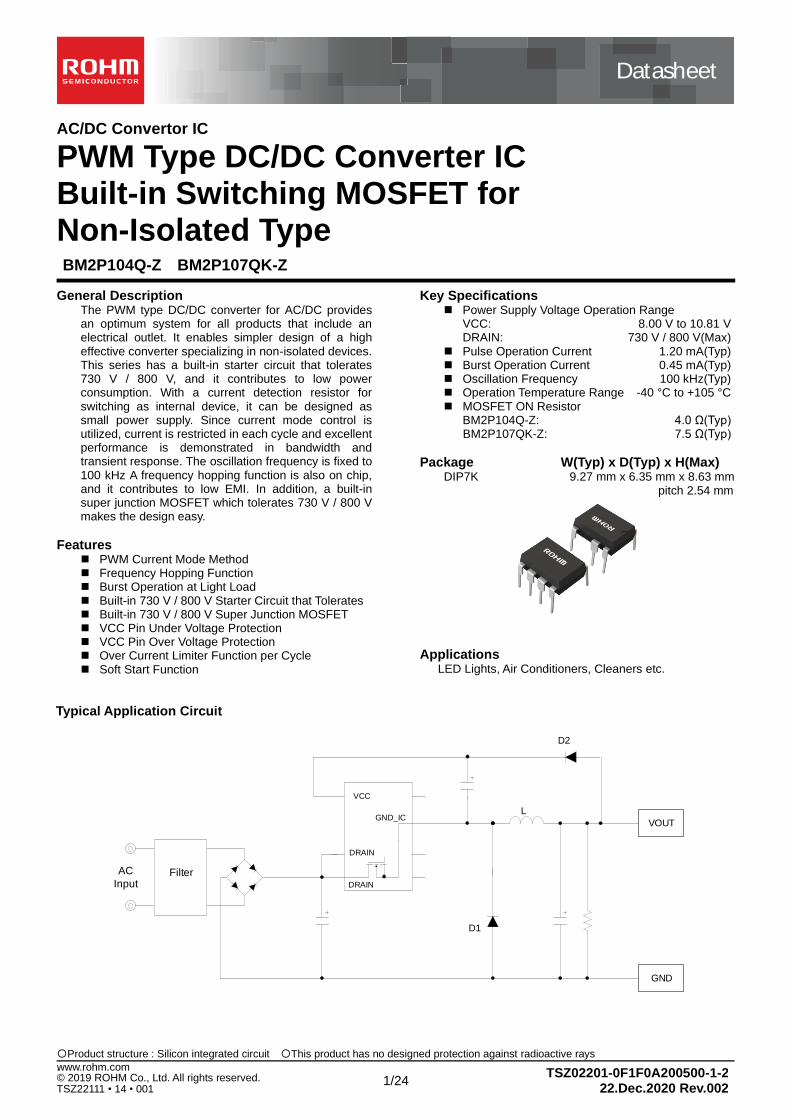
Pin Configuration
Pin Descriptions
Pin No. Pin Name I/O Function ESD Diode
VCC GND_IC
1 N.C. - Non Connection - -
2 N.C. - Non Connection - -
3 GND_IC I/O GND pin ○ -
4 N.C. - Non Connection - -
5 VCC I Power supply input pin - ○
6 DRAIN I/O MOSFET DRAIN pin - ○
7 DRAIN I/O MOSFET DRAIN pin - ○
Block Diagram
12
36
45
7
VCC
DRAIN
GND_IC
(TOP VIEW)
DRAIN
N.C.
N.C.
N.C.
PWM Control
VCC UVLO
DRAIN
DRIVER
S
QR
+
-
PWMComparator
+
-
+
-
BurstComparator
GND_IC
+
-
+-
OLP
Internal Block
+-
VCC OVP
Soft Start
OSCFrequencyHopping
100 μsFilter
128 ms/512 msTimer
MAXDUTY
3
Internal
Regulator
6,7
Starter
VCC 5
Super
Junction
MOSFET
+-
Reference
Voltage
Leading-EdgeBlanking Time
Current
Limitter
Reference
Voltage
CurrentSensing
ThermalProtection
+
-
Dynamic Current
Limitter
Reference
Voltage
Logic&
Timer
3/24
BM2P104Q-Z BM2P107QK-Z
TSZ02201-0F1F0A200500-1-2 22.Dec.2020 Rev.002
© 2019 ROHM Co., Ltd. All rights reserved. www.rohm.com
TSZ22111 • 15 • 001
Description of Blocks
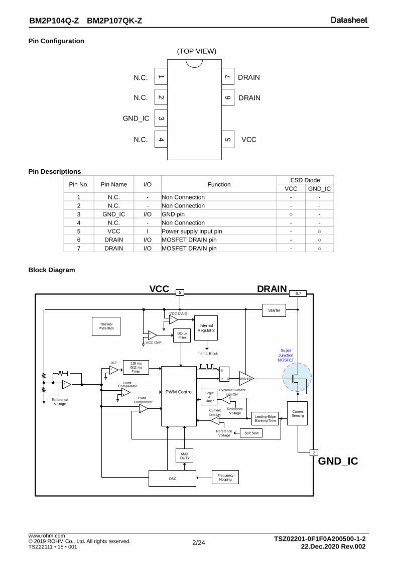
1 Back Converter This is the IC for exclusive use of non-isolated type back converter.
<Basic operation of back converter>
1.1 When the MOSFET for Switching is ON
When the MOSFET turns ON, current IL flows to coil L and energy is stored. At this moment, the voltage of the GND_IC pin becomes the voltage near the DRAIN pin, and the diode D1 is OFF.
𝐼𝐿 =(𝑉𝐼𝑁 − 𝑉𝑂𝑈𝑇)
𝐿× 𝑡𝑜𝑛
Where:
𝑉𝐼𝑁 is the DRAIN Voltage 𝑉𝑂𝑈𝑇 is the Output Voltage
𝐼𝐿 is the Inductor Current
𝑡𝑜𝑛 is ON-Time of MOSFET
Figure 1. Back Converter Operation (MOSFET=ON)
L
GND
VOUT
AC
InputFilter
D1
D2
5
7 1
3
4
DRAIN
VCC
GND_IC
26DRAIN
ONCurrent
IL
VIN
4/24
BM2P104Q-Z BM2P107QK-Z
TSZ02201-0F1F0A200500-1-2 22.Dec.2020 Rev.002
© 2019 ROHM Co., Ltd. All rights reserved. www.rohm.com
TSZ22111 • 15 • 001
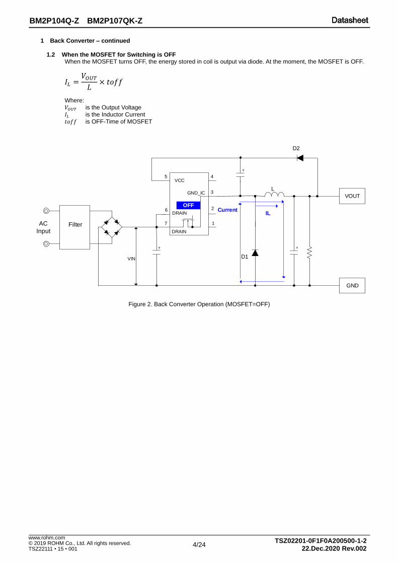
1 Back Converter – continued
1.2 When the MOSFET for Switching is OFF When the MOSFET turns OFF, the energy stored in coil is output via diode. At the moment, the MOSFET is OFF.
𝐼𝐿 =𝑉𝑂𝑈𝑇
𝐿× 𝑡𝑜𝑓𝑓
Where: 𝑉𝑂𝑈𝑇 is the Output Voltage
𝐼𝐿 is the Inductor Current
𝑡𝑜𝑓𝑓 is OFF-Time of MOSFET
Figure 2. Back Converter Operation (MOSFET=OFF)
L
GND
VOUT
AC
InputFilter
D1
D2
5
7 1
3
4
DRAIN
VCC
GND_IC
26DRAIN
OFFCurrent
IL
VIN
5/24
BM2P104Q-Z BM2P107QK-Z
TSZ02201-0F1F0A200500-1-2 22.Dec.2020 Rev.002
© 2019 ROHM Co., Ltd. All rights reserved. www.rohm.com
TSZ22111 • 15 • 001
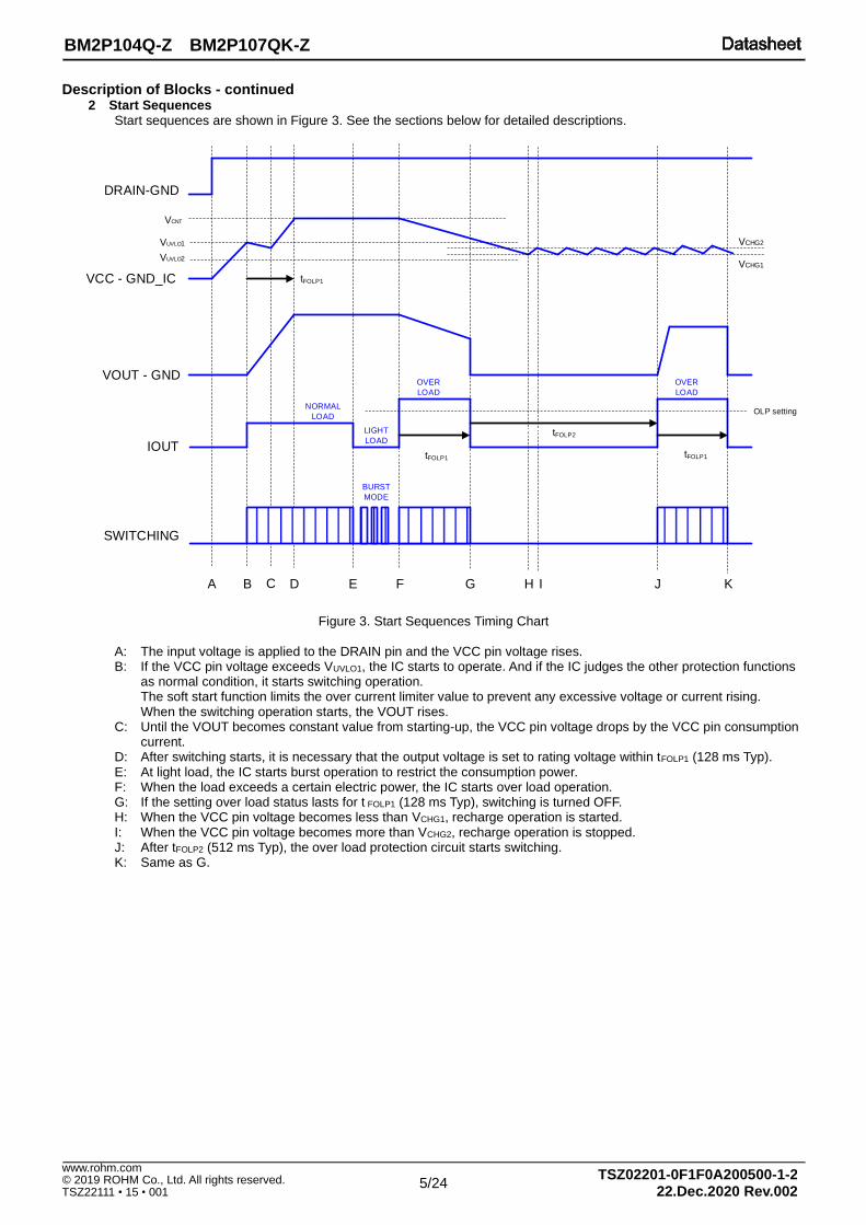
Description of Blocks - continued 2 Start Sequences
Start sequences are shown in Figure 3. See the sections below for detailed descriptions.
Figure 3. Start Sequences Timing Chart
A: The input voltage is applied to the DRAIN pin and the VCC pin voltage rises. B: If the VCC pin voltage exceeds VUVLO1, the IC starts to operate. And if the IC judges the other protection functions
as normal condition, it starts switching operation. The soft start function limits the over current limiter value to prevent any excessive voltage or current rising. When the switching operation starts, the VOUT rises.
C: Until the VOUT becomes constant value from starting-up, the VCC pin voltage drops by the VCC pin consumption current.
D: After switching starts, it is necessary that the output voltage is set to rating voltage within tFOLP1 (128 ms Typ). E: At light load, the IC starts burst operation to restrict the consumption power. F: When the load exceeds a certain electric power, the IC starts over load operation. G: If the setting over load status lasts for t FOLP1 (128 ms Typ), switching is turned OFF. H: When the VCC pin voltage becomes less than VCHG1, recharge operation is started. I: When the VCC pin voltage becomes more than VCHG2, recharge operation is stopped. J: After tFOLP2 (512 ms Typ), the over load protection circuit starts switching. K: Same as G.
DRAIN-GND
VCC - GND_IC
VOUT - GND
IOUT
NORMAL
LOAD
LIGHT
LOAD
OVER
LOAD
SWITCHING
tFOLP1
OVER
LOAD
OLP setting
BURST
MODE
A B C D E F G H I J K
VCHG1
VCHG2VUVLO1
VUVLO2
VCNT
tFOLP1
tFOLP2
tFOLP1
6/24
BM2P104Q-Z BM2P107QK-Z
TSZ02201-0F1F0A200500-1-2 22.Dec.2020 Rev.002
© 2019 ROHM Co., Ltd. All rights reserved. www.rohm.com
TSZ22111 • 15 • 001
Description of Blocks – continued
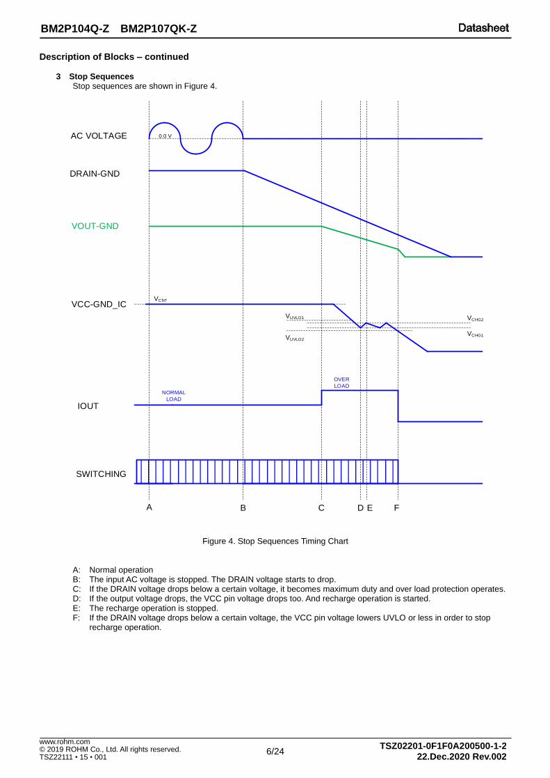
3 Stop Sequences Stop sequences are shown in Figure 4.
Figure 4. Stop Sequences Timing Chart
A: Normal operation B: The input AC voltage is stopped. The DRAIN voltage starts to drop. C: If the DRAIN voltage drops below a certain voltage, it becomes maximum duty and over load protection operates. D: If the output voltage drops, the VCC pin voltage drops too. And recharge operation is started. E: The recharge operation is stopped. F: If the DRAIN voltage drops below a certain voltage, the VCC pin voltage lowers UVLO or less in order to stop
recharge operation.
DRAIN-GND
VCC-GND_IC
VOUT-GND
IOUT
NORMAL
LOAD
OVER
LOAD
SWITCHING
A B C D E F
AC VOLTAGE 0.0 V
VUVLO1
VUVLO2
VCHG2
VCHG1
VCNT
7/24
BM2P104Q-Z BM2P107QK-Z
TSZ02201-0F1F0A200500-1-2 22.Dec.2020 Rev.002
© 2019 ROHM Co., Ltd. All rights reserved. www.rohm.com
TSZ22111 • 15 • 001
Description of Blocks – continued
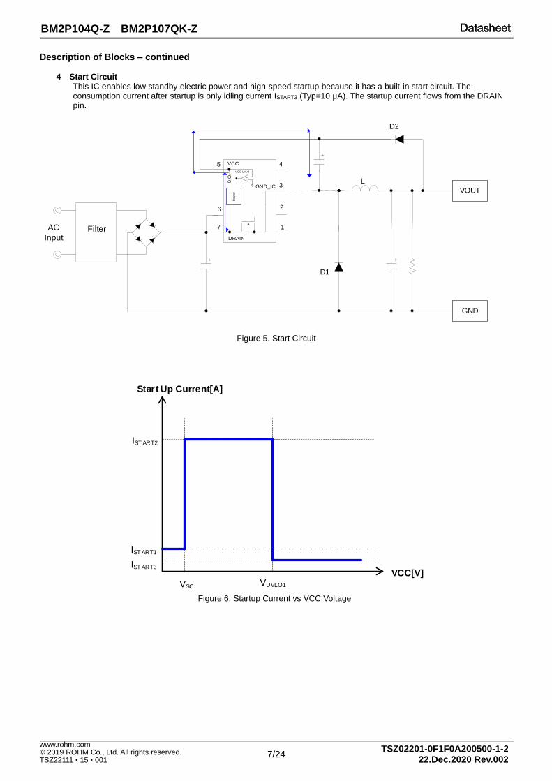
4 Start Circuit This IC enables low standby electric power and high-speed startup because it has a built-in start circuit. The consumption current after startup is only idling current ISTART3 (Typ=10 μA). The startup current flows from the DRAIN pin.
Figure 5. Start Circuit
Figure 6. Startup Current vs VCC Voltage
L
GND
VOUT
AC
InputFilter
D1
D2
5
7 1
3
4
DRAIN
VCC
GND_IC
26
VCC UVLO
+-
Sta
rter
VCC[V]
IST ART1
IST ART2
VUVLO1VSC
Start Up Current[A]
IST ART3
8/24
BM2P104Q-Z BM2P107QK-Z
TSZ02201-0F1F0A200500-1-2 22.Dec.2020 Rev.002
© 2019 ROHM Co., Ltd. All rights reserved. www.rohm.com
TSZ22111 • 15 • 001
Description of Blocks – continued
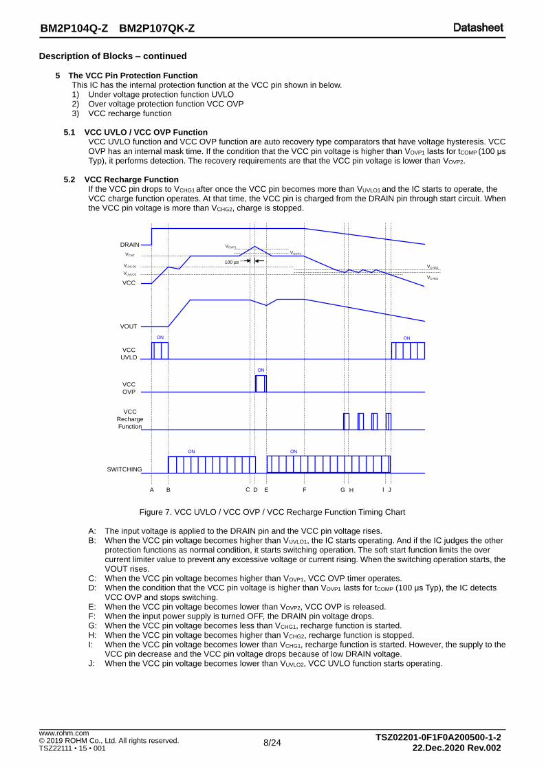
5 The VCC Pin Protection Function This IC has the internal protection function at the VCC pin shown in below. 1) Under voltage protection function UVLO 2) Over voltage protection function VCC OVP 3) VCC recharge function
5.1 VCC UVLO / VCC OVP Function
VCC UVLO function and VCC OVP function are auto recovery type comparators that have voltage hysteresis. VCC OVP has an internal mask time. If the condition that the VCC pin voltage is higher than VOVP1 lasts for tCOMP (100 μs Typ), it performs detection. The recovery requirements are that the VCC pin voltage is lower than VOVP2.
5.2 VCC Recharge Function If the VCC pin drops to VCHG1 after once the VCC pin becomes more than VUVLO1 and the IC starts to operate, the VCC charge function operates. At that time, the VCC pin is charged from the DRAIN pin through start circuit. When the VCC pin voltage is more than VCHG2, charge is stopped.
Figure 7. VCC UVLO / VCC OVP / VCC Recharge Function Timing Chart
A: The input voltage is applied to the DRAIN pin and the VCC pin voltage rises. B: When the VCC pin voltage becomes higher than VUVLO1, the IC starts operating. And if the IC judges the other
protection functions as normal condition, it starts switching operation. The soft start function limits the over current limiter value to prevent any excessive voltage or current rising. When the switching operation starts, the VOUT rises.
C: When the VCC pin voltage becomes higher than VOVP1, VCC OVP timer operates. D: When the condition that the VCC pin voltage is higher than VOVP1 lasts for tCOMP (100 μs Typ), the IC detects
VCC OVP and stops switching. E: When the VCC pin voltage becomes lower than VOVP2, VCC OVP is released. F: When the input power supply is turned OFF, the DRAIN pin voltage drops. G: When the VCC pin voltage becomes less than VCHG1, recharge function is started. H: When the VCC pin voltage becomes higher than VCHG2, recharge function is stopped. I: When the VCC pin voltage becomes lower than VCHG1, recharge function is started. However, the supply to the
VCC pin decrease and the VCC pin voltage drops because of low DRAIN voltage. J: When the VCC pin voltage becomes lower than VUVLO2, VCC UVLO function starts operating.
DRAIN
VCC
VOUT
SWITCHING
A B C D E F G H I J
100 µs
VCC
UVLO
ON
VCC
OVP
ON
ON
ON
ON
VCC
Recharge
Function
VCHG2
VCHG1
VUVLO1
VUVLO2
VCNT
VOVP1
VOVP2
9/24
BM2P104Q-Z BM2P107QK-Z
TSZ02201-0F1F0A200500-1-2 22.Dec.2020 Rev.002
© 2019 ROHM Co., Ltd. All rights reserved. www.rohm.com
TSZ22111 • 15 • 001
Description of Blocks – continued
6 DC/DC Driver This performs current mode PWM control. An internal oscillator sets a fixed oscillation frequency fSW (100 kHz Typ). This IC has a built-in oscillation frequency hopping function. The maximum duty is DMAX (75 % Typ). To achieve the low consumption power at light load, it also has an internal burst mode circuit.
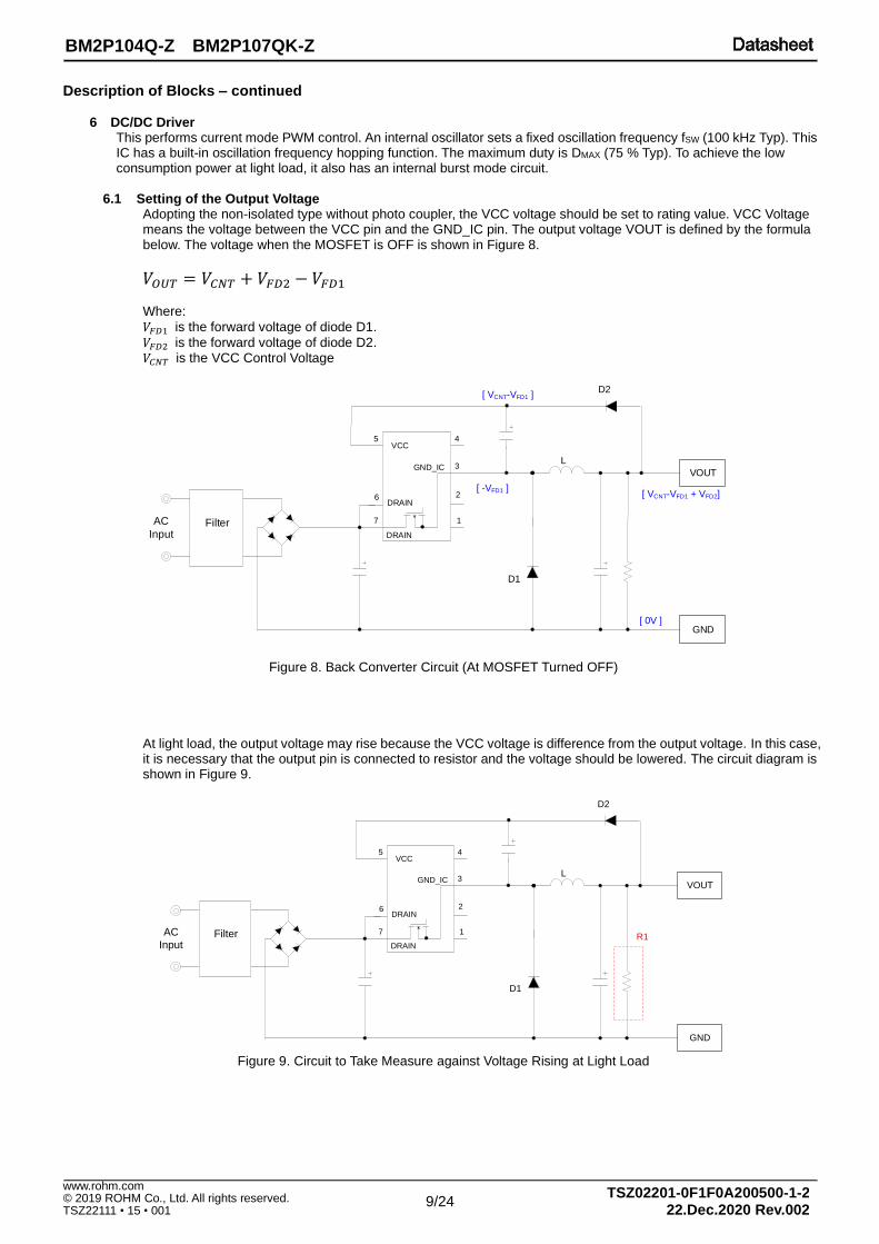
6.1 Setting of the Output Voltage Adopting the non-isolated type without photo coupler, the VCC voltage should be set to rating value. VCC Voltage means the voltage between the VCC pin and the GND_IC pin. The output voltage VOUT is defined by the formula below. The voltage when the MOSFET is OFF is shown in Figure 8.
𝑉𝑂𝑈𝑇 = 𝑉𝐶𝑁𝑇 + 𝑉𝐹𝐷2 − 𝑉𝐹𝐷1 Where:
𝑉𝐹𝐷1 is the forward voltage of diode D1.
𝑉𝐹𝐷2 is the forward voltage of diode D2. 𝑉𝐶𝑁𝑇 is the VCC Control Voltage
Figure 8. Back Converter Circuit (At MOSFET Turned OFF)
At light load, the output voltage may rise because the VCC voltage is difference from the output voltage. In this case, it is necessary that the output pin is connected to resistor and the voltage should be lowered. The circuit diagram is shown in Figure 9.
Figure 9. Circuit to Take Measure against Voltage Rising at Light Load
L
GND
VOUT
AC
InputFilter
D1
D2
5
7 1
3
4
DRAIN
VCC
GND_IC
26DRAIN
[ 0V ]
[ -VFD1 ]
[ VCNT-VFD1 ]
[ VCNT-VFD1 + VFD2]
L
GND
VOUT
AC
InputFilter
D1
D2
5
7 1
3
4
DRAIN
VCC
GND_IC
26DRAIN
R1
10/24
BM2P104Q-Z BM2P107QK-Z
TSZ02201-0F1F0A200500-1-2 22.Dec.2020 Rev.002
© 2019 ROHM Co., Ltd. All rights reserved. www.rohm.com
TSZ22111 • 15 • 001
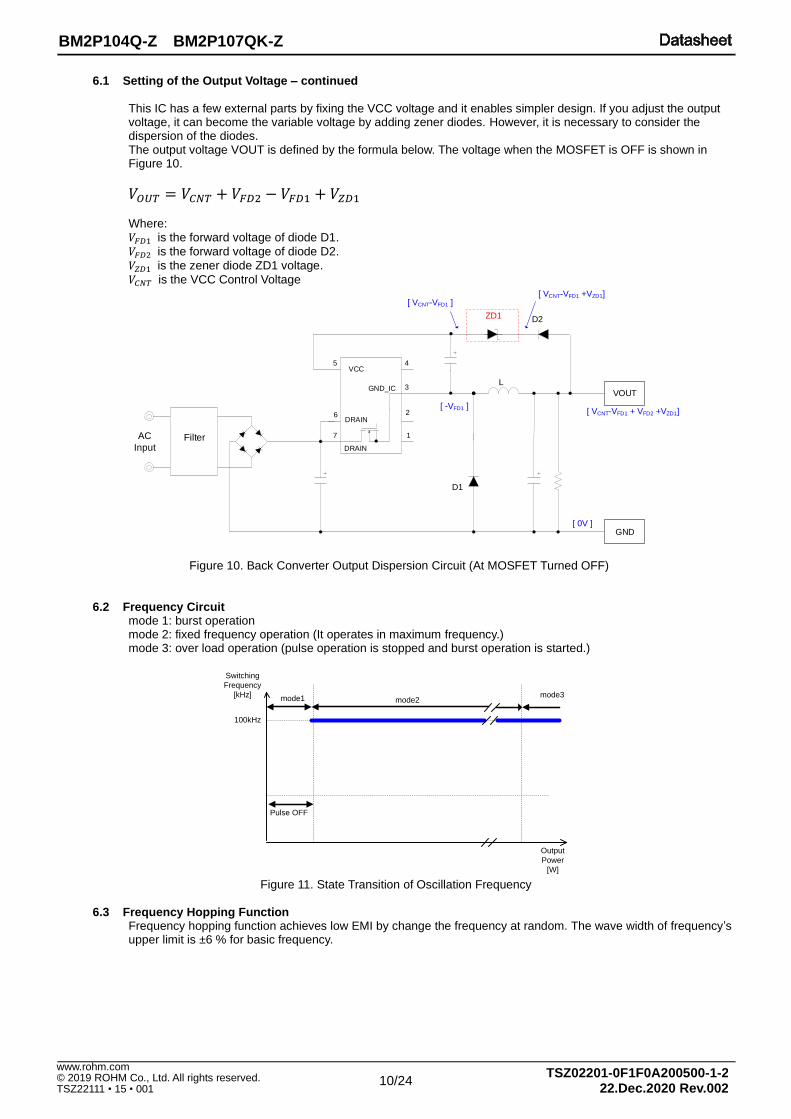
6.1 Setting of the Output Voltage – continued This IC has a few external parts by fixing the VCC voltage and it enables simpler design. If you adjust the output voltage, it can become the variable voltage by adding zener diodes. However, it is necessary to consider the dispersion of the diodes. The output voltage VOUT is defined by the formula below. The voltage when the MOSFET is OFF is shown in Figure 10.
𝑉𝑂𝑈𝑇 = 𝑉𝐶𝑁𝑇 + 𝑉𝐹𝐷2 − 𝑉𝐹𝐷1 + 𝑉𝑍𝐷1 Where: 𝑉𝐹𝐷1 is the forward voltage of diode D1.
𝑉𝐹𝐷2 is the forward voltage of diode D2.
𝑉𝑍𝐷1 is the zener diode ZD1 voltage.
𝑉𝐶𝑁𝑇 is the VCC Control Voltage
Figure 10. Back Converter Output Dispersion Circuit (At MOSFET Turned OFF)
6.2 Frequency Circuit
mode 1: burst operation mode 2: fixed frequency operation (It operates in maximum frequency.) mode 3: over load operation (pulse operation is stopped and burst operation is started.)
Figure 11. State Transition of Oscillation Frequency
6.3 Frequency Hopping Function
Frequency hopping function achieves low EMI by change the frequency at random. The wave width of frequency’s upper limit is ±6 % for basic frequency.
L
GND
VOUT
AC
InputFilter
D1
D2
5
7 1
3
4
DRAIN
VCC
GND_IC
26DRAIN
[ 0V ]
[ -VFD1 ]
[ VCNT-VFD1 ]
[ VCNT-VFD1 + VFD2 +VZD1]
[ VCNT-VFD1 +VZD1]
ZD1
Output
Power
[W]
Switching
Frequency
[kHz]
100kHz
mode1 mode2mode3
Pulse OFF
11/24
BM2P104Q-Z BM2P107QK-Z
TSZ02201-0F1F0A200500-1-2 22.Dec.2020 Rev.002
© 2019 ROHM Co., Ltd. All rights reserved. www.rohm.com
TSZ22111 • 15 • 001
6 DC/DC Driver – continued
6.4 PWM Error Amp and PWM Comparator The internal error Amp achieves the reduction of external parts. In addition, this IC adopts current mode method. It makes the design easy.
6.5 Over Current Limiter
This IC has an internal over current limiter per switching cycle. This function monitors the coil current and if it exceeds a certain current, the IC stops switching. Additionally, an internal current detection resistor contributes to reduction of parts and improvement of efficiency. The peak current by which the IC switches to the over load mode is determined by the formula below.
𝑃𝑒𝑎𝑘 𝑐𝑢𝑟𝑟𝑒𝑛𝑡 = 𝐼𝑃𝐸𝐴𝐾 + (𝑉𝐷𝑅𝐴𝐼𝑁 − 𝑉𝑂𝑈𝑇)
𝐿× 𝑡𝑑𝑒𝑙𝑎𝑦
Where:
𝐼𝑃𝐸𝐴𝐾 is the over current limiter internal the IC.
𝑉𝐷𝑅𝐴𝐼𝑁 is the DRAIN voltage. 𝑉𝑂𝑈𝑇 is the output voltage.
𝐿 is the Coil value.
𝑡𝑑𝑒𝑙𝑎𝑦 is the Delay time after detection of over current limiter.
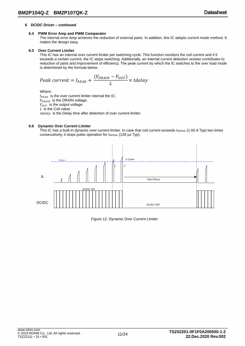
6.6 Dynamic Over Current Limiter This IC has a built-in dynamic over current limiter. In case that coil current exceeds IDPEAK (1.60 A Typ) two times consecutively, it stops pulse operation for tDPEAK (128 μs Typ).
Figure 12. Dynamic Over Current Limiter
IL
IDPEAK 2 Count
Typ=128 µs
1 2
DC/DC
DC/DC ON
DC/DC OFF
12/24
BM2P104Q-Z BM2P107QK-Z
TSZ02201-0F1F0A200500-1-2 22.Dec.2020 Rev.002
© 2019 ROHM Co., Ltd. All rights reserved. www.rohm.com
TSZ22111 • 15 • 001
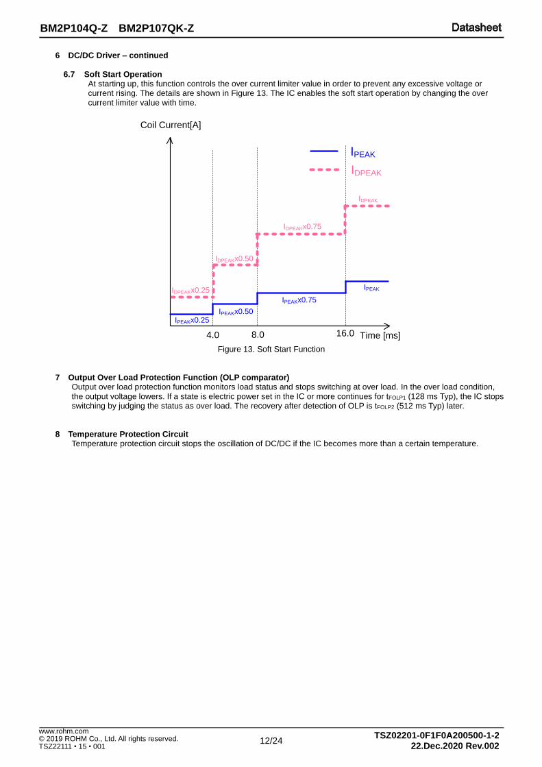
6 DC/DC Driver – continued
6.7 Soft Start Operation At starting up, this function controls the over current limiter value in order to prevent any excessive voltage or current rising. The details are shown in Figure 13. The IC enables the soft start operation by changing the over current limiter value with time.
Figure 13. Soft Start Function
7 Output Over Load Protection Function (OLP comparator) Output over load protection function monitors load status and stops switching at over load. In the over load condition, the output voltage lowers. If a state is electric power set in the IC or more continues for tFOLP1 (128 ms Typ), the IC stops switching by judging the status as over load. The recovery after detection of OLP is tFOLP2 (512 ms Typ) later.
8 Temperature Protection Circuit Temperature protection circuit stops the oscillation of DC/DC if the IC becomes more than a certain temperature.
Time [ms]
Coil Current[A]
4.0 8.0 16.0
IPEAK
IPEAK
IDPEAK
IPEAKx0.25
IDPEAK
IPEAKx0.50
IPEAKx0.75
IDPEAKx0.25
IDPEAKx0.50
IDPEAKx0.75
13/24
BM2P104Q-Z BM2P107QK-Z
TSZ02201-0F1F0A200500-1-2 22.Dec.2020 Rev.002
© 2019 ROHM Co., Ltd. All rights reserved. www.rohm.com
TSZ22111 • 15 • 001
Description of Blocks – continued
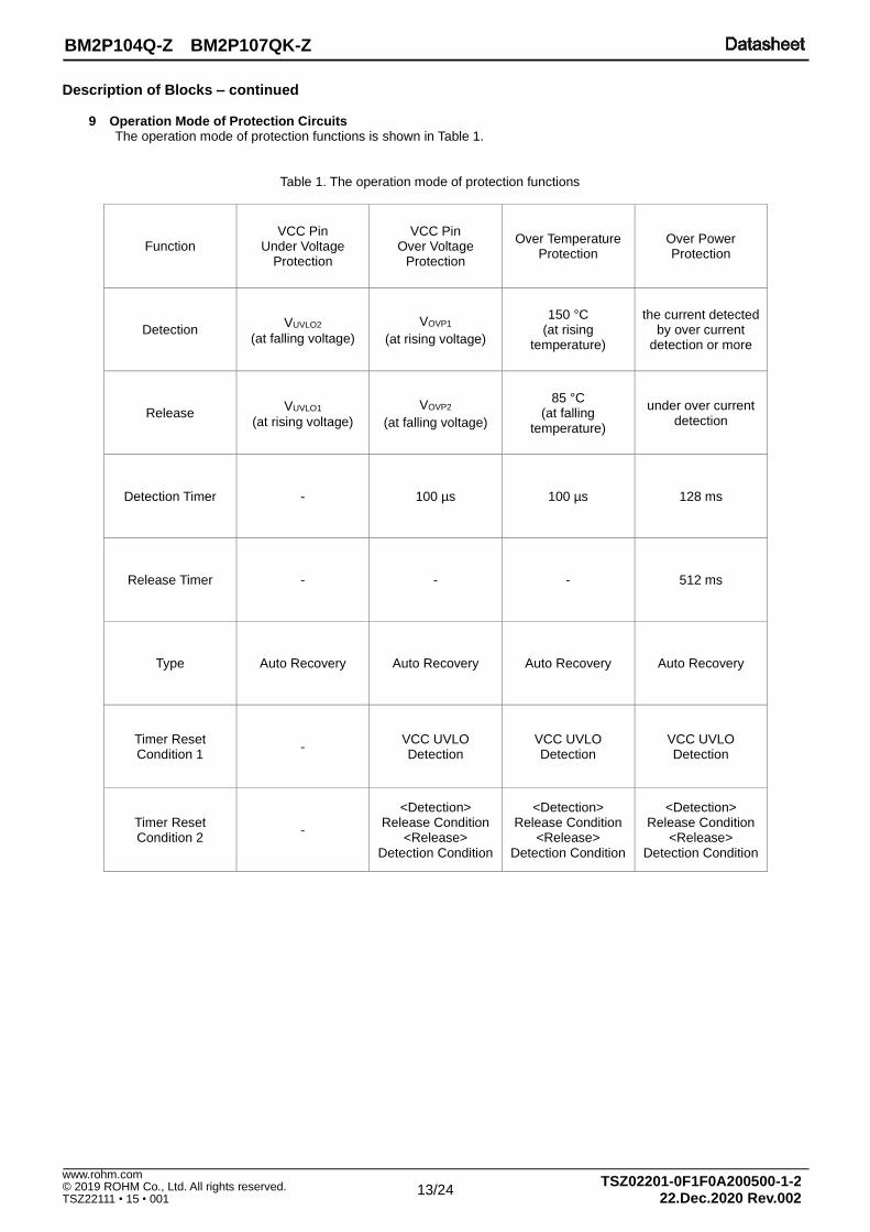
9 Operation Mode of Protection Circuits
The operation mode of protection functions is shown in Table 1.
Table 1. The operation mode of protection functions
Function VCC Pin
Under Voltage Protection
VCC Pin Over Voltage
Protection
Over Temperature Protection
Over Power Protection
Detection VUVLO2
(at falling voltage)
VOVP1
(at rising voltage)
150 °C (at rising
temperature)
the current detected by over current
detection or more
Release VUVLO1
(at rising voltage)
VOVP2
(at falling voltage)
85 °C (at falling
temperature)
under over current detection
Detection Timer - 100 µs 100 µs 128 ms
Release Timer - - - 512 ms
Type Auto Recovery Auto Recovery Auto Recovery Auto Recovery
Timer Reset Condition 1
- VCC UVLO Detection
VCC UVLO Detection
VCC UVLO Detection
Timer Reset Condition 2
-
<Detection> Release Condition
<Release> Detection Condition
<Detection> Release Condition
<Release> Detection Condition
<Detection> Release Condition
<Release> Detection Condition
14/24
BM2P104Q-Z BM2P107QK-Z
TSZ02201-0F1F0A200500-1-2 22.Dec.2020 Rev.002
© 2019 ROHM Co., Ltd. All rights reserved. www.rohm.com
TSZ22111 • 15 • 001
Description of Blocks – continued
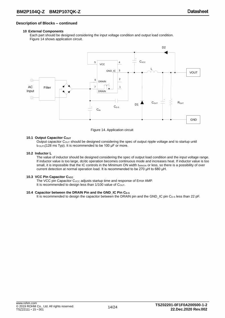
10 External Components Each part should be designed considering the input voltage condition and output load condition. Figure 14 shows application circuit.
Figure 14. Application circuit
10.1 Output Capacitor COUT
Output capacitor COUT should be designed considering the spec of output ripple voltage and to startup until tFOLP1(128 ms Typ). It is recommended to be 100 μF or more.
10.2 Inductor L
The value of inductor should be designed considering the spec of output load condition and the input voltage range. If inductor value is too large, dc/dc operation becomes continuous mode and increases heat. If inductor value is too small, it is impossible that the IC controls in the Minimum ON width tMINON or less, so there is a possibility of over current detection at normal operation load. It is recommended to be 270 μH to 680 μH.
10.3 VCC Pin Capacitor CVCC
The VCC pin Capacitor CVCC adjusts startup time and response of Error AMP. It is recommended to design less than 1/100 value of COUT.
10.4 Capacitor between the DRAIN Pin and the GND_IC Pin CD-S It is recommended to design the capacitor between the DRAIN pin and the GND_IC pin CD-S less than 22 pF.
L
GND
VOUT
AC
InputFilter
D1
D2
5
7 1
3
4
DRAIN
VCC
GND_IC
26DRAIN
COUT ROUT
CVCC
CIN
CD-S
15/24
BM2P104Q-Z BM2P107QK-Z
TSZ02201-0F1F0A200500-1-2 22.Dec.2020 Rev.002
© 2019 ROHM Co., Ltd. All rights reserved. www.rohm.com
TSZ22111 • 15 • 001
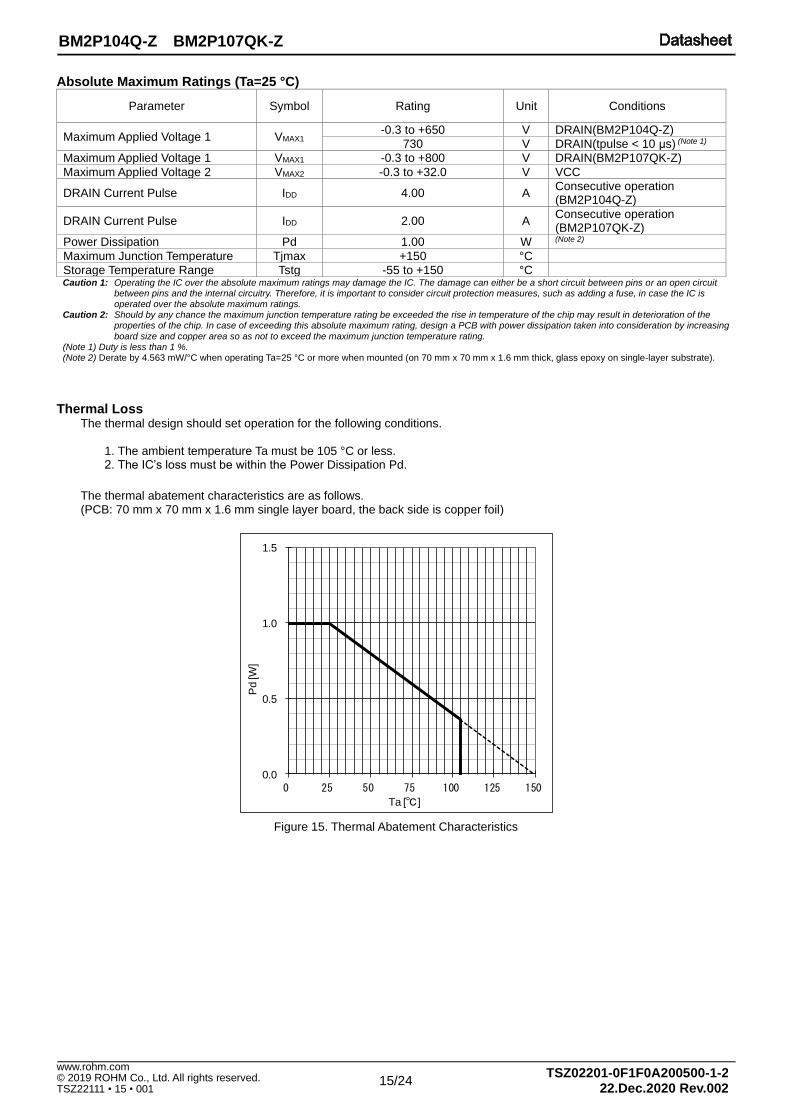
Absolute Maximum Ratings (Ta=25 °C)
Parameter Symbol Rating Unit Conditions
Maximum Applied Voltage 1 VMAX1 -0.3 to +650 V DRAIN(BM2P104Q-Z)
730 V DRAIN(tpulse < 10 μs) (Note 1)
Maximum Applied Voltage 1 VMAX1 -0.3 to +800 V DRAIN(BM2P107QK-Z)
Maximum Applied Voltage 2 VMAX2 -0.3 to +32.0 V VCC
DRAIN Current Pulse IDD 4.00 A Consecutive operation (BM2P104Q-Z)
DRAIN Current Pulse IDD 2.00 A Consecutive operation (BM2P107QK-Z)
Power Dissipation Pd 1.00 W (Note 2)
Maximum Junction Temperature Tjmax +150 °C
Storage Temperature Range Tstg -55 to +150 °C Caution 1: Operating the IC over the absolute maximum ratings may damage the IC. The damage can either be a short circuit between pins or an open circuit
between pins and the internal circuitry. Therefore, it is important to consider circuit protection measures, such as adding a fuse, in case the IC is operated over the absolute maximum ratings.
Caution 2: Should by any chance the maximum junction temperature rating be exceeded the rise in temperature of the chip may result in deterioration of the properties of the chip. In case of exceeding this absolute maximum rating, design a PCB with power dissipation taken into consideration by increasing
board size and copper area so as not to exceed the maximum junction temperature rating. (Note 1) Duty is less than 1 %. (Note 2) Derate by 4.563 mW/°C when operating Ta=25 °C or more when mounted (on 70 mm x 70 mm x 1.6 mm thick, glass epoxy on single-layer substrate).
Thermal Loss The thermal design should set operation for the following conditions.
1. The ambient temperature Ta must be 105 °C or less. 2. The IC’s loss must be within the Power Dissipation Pd.
The thermal abatement characteristics are as follows. (PCB: 70 mm x 70 mm x 1.6 mm single layer board, the back side is copper foil)
Figure 15. Thermal Abatement Characteristics
0.0
0.5
1.0
1.5
0 25 50 75 100 125 150
Pd [W
]
Ta [℃]
16/24
BM2P104Q-Z BM2P107QK-Z
TSZ02201-0F1F0A200500-1-2 22.Dec.2020 Rev.002
© 2019 ROHM Co., Ltd. All rights reserved. www.rohm.com
TSZ22111 • 15 • 001
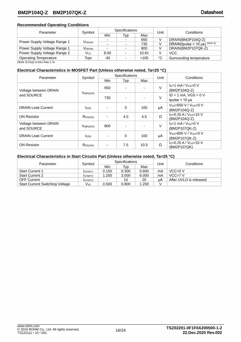
Recommended Operating Conditions
Parameter Symbol Specifications
Unit Conditions Min Typ Max
Power Supply Voltage Range 1 VDRAIN - - 650 V DRAIN(BM2P104Q-Z)
- - 730 V DRAIN(tpulse < 10 μs) (Note 3)
Power Supply Voltage Range 1 VDRAIN - - 800 V DRAIN(BM2P107QK-Z)
Power Supply Voltage Range 2 VCC 8.00 - 10.81 V VCC
Operating Temperature Topr -40 - +105 °C Surrounding temperature (Note 3) Duty is less than 1 %
Electrical Characteristics in MOSFET Part (Unless otherwise noted, Ta=25 °C)
Parameter Symbol Specifications
Unit Conditions Min Typ Max
Voltage between DRAIN
and SOURCE V(BR)DDS
650 - - V ID=1 mA / VGS=0 V
(BM2P104Q-Z)
730 - - V ID = 1 mA, VGS = 0 V
tpulse < 10 μs
DRAIN Leak Current IDSS - 0 100 μA VDS=650 V / VGS=0 V
(BM2P104Q-Z)
ON Resistor RDS(ON) - 4.0 4.5 Ω ID=0.25 A / VGS=10 V (BM2P104Q-Z)
Voltage between DRAIN
and SOURCE V(BR)DDS 800 - - V
ID=1 mA / VGS=0 V
(BM2P107QK-Z)
DRAIN Leak Current IDSS - 0 100 μA VDS=800 V / VGS=0 V
(BM2P107QK-Z)
ON Resistor RDS(ON) - 7.5 10.5 Ω ID=0.25 A / VGS=10 V (BM2P107QK)
Electrical Characteristics in Start Circuits Part (Unless otherwise noted, Ta=25 °C)
Parameter Symbol Specifications
Unit Conditions Min Typ Max
Start Current 1 ISTART1 0.150 0.300 0.600 mA VCC=0 V
Start Current 2 ISTART2 1.200 3.000 6.000 mA VCC=7 V
OFF Current ISTART3 - 10 20 μA After UVLO is released
Start Current Switching Voltage VSC 0.500 0.800 1.200 V
17/24
BM2P104Q-Z BM2P107QK-Z
TSZ02201-0F1F0A200500-1-2 22.Dec.2020 Rev.002
© 2019 ROHM Co., Ltd. All rights reserved. www.rohm.com
TSZ22111 • 15 • 001
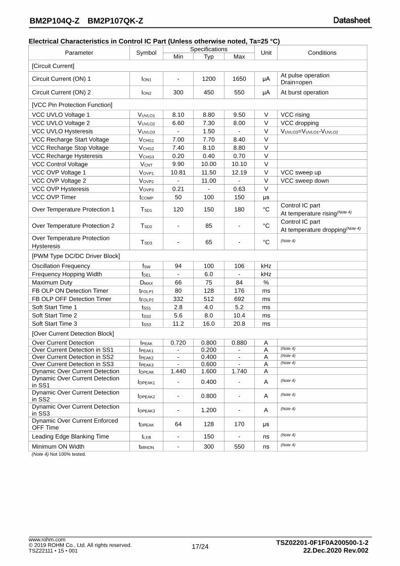
Electrical Characteristics in Control IC Part (Unless otherwise noted, Ta=25 °C)
Parameter Symbol Specifications
Unit Conditions Min Typ Max
[Circuit Current]
Circuit Current (ON) 1 ION1 - 1200 1650 μA At pulse operation Drain=open
Circuit Current (ON) 2 ION2 300 450 550 μA At burst operation
[VCC Pin Protection Function]
VCC UVLO Voltage 1 VUVLO1 8.10 8.80 9.50 V VCC rising
VCC UVLO Voltage 2 VUVLO2 6.60 7.30 8.00 V VCC dropping
VCC UVLO Hysteresis VUVLO3 - 1.50 - V VUVLO3=VUVLO1-VUVLO2
VCC Recharge Start Voltage VCHG1 7.00 7.70 8.40 V
VCC Recharge Stop Voltage VCHG2 7.40 8.10 8.80 V
VCC Recharge Hysteresis VCHG3 0.20 0.40 0.70 V
VCC Control Voltage VCNT 9.90 10.00 10.10 V
VCC OVP Voltage 1 VOVP1 10.81 11.50 12.19 V VCC sweep up
VCC OVP Voltage 2 VOVP2 - 11.00 - V VCC sweep down
VCC OVP Hysteresis VOVP3 0.21 - 0.63 V
VCC OVP Timer tCOMP 50 100 150 μs
Over Temperature Protection 1 TSD1 120 150 180 °C Control IC part
At temperature rising(Note 4)
Over Temperature Protection 2 TSD2 - 85 - °C Control IC part
At temperature dropping(Note 4)
Over Temperature Protection
Hysteresis TSD3 - 65 - °C (Note 4)
[PWM Type DC/DC Driver Block]
Oscillation Frequency fSW 94 100 106 kHz
Frequency Hopping Width fDEL - 6.0 - kHz
Maximum Duty DMAX 66 75 84 %
FB OLP ON Detection Timer tFOLP1 80 128 176 ms
FB OLP OFF Detection Timer tFOLP2 332 512 692 ms
Soft Start Time 1 tSS1 2.8 4.0 5.2 ms
Soft Start Time 2 tSS2 5.6 8.0 10.4 ms
Soft Start Time 3 tSS3 11.2 16.0 20.8 ms
[Over Current Detection Block]
Over Current Detection IPEAK 0.720 0.800 0.880 A
Over Current Detection in SS1 IPEAK1 - 0.200 - A (Note 4)
Over Current Detection in SS2 IPEAK2 - 0.400 - A (Note 4)
Over Current Detection in SS3 IPEAK3 - 0.600 - A (Note 4)
Dynamic Over Current Detection IDPEAK 1.440 1.600 1.740 A
Dynamic Over Current Detection in SS1
IDPEAK1 - 0.400 - A (Note 4)
Dynamic Over Current Detection in SS2
IDPEAK2 - 0.800 - A (Note 4)
Dynamic Over Current Detection in SS3
IDPEAK3 - 1.200 - A (Note 4)
Dynamic Over Current Enforced OFF Time
tDPEAK 64 128 170 μs
Leading Edge Blanking Time tLEB - 150 - ns (Note 4)
Minimum ON Width tMINON - 300 550 ns (Note 4)
(Note 4) Not 100% tested.
18/24
BM2P104Q-Z BM2P107QK-Z
TSZ02201-0F1F0A200500-1-2 22.Dec.2020 Rev.002
© 2019 ROHM Co., Ltd. All rights reserved. www.rohm.com
TSZ22111 • 15 • 001
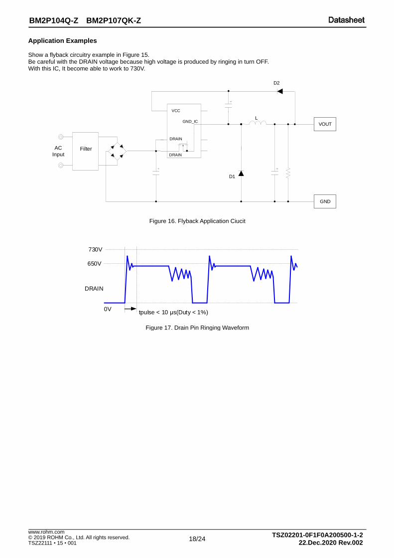
0V
730V
tpulse < 10 μs(Duty < 1%)
DRAIN
650V
L
GND
VOUT
AC
InputFilter
D1
D2
DRAIN
VCC
GND_IC
DRAIN
Figure 16. Flyback Application Ciucit
Figure 17. Drain Pin Ringing Waveform
Application Examples Show a flyback circuitry example in Figure 15. Be careful with the DRAIN voltage because high voltage is produced by ringing in turn OFF. With this IC, It become able to work to 730V.
19/24
BM2P104Q-Z BM2P107QK-Z
TSZ02201-0F1F0A200500-1-2 22.Dec.2020 Rev.002
© 2019 ROHM Co., Ltd. All rights reserved. www.rohm.com
TSZ22111 • 15 • 001
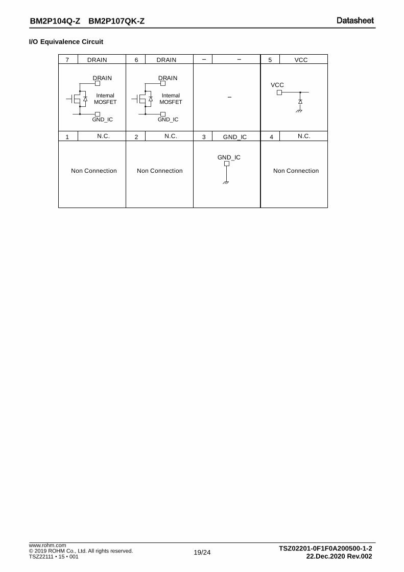
I/O Equivalence Circuit
7 6 5
GND_IC
VCC
VCC
DRAIN
GND_IC
DRAIN
GND_IC
Internal MOSFET
1 2 3 4
Non ConnectionNon Connection
DRAIN
GND_IC
Internal MOSFET
DRAIN
Non Connection
N.C. N.C. N.C.
-
--
20/24
BM2P104Q-Z BM2P107QK-Z
TSZ02201-0F1F0A200500-1-2 22.Dec.2020 Rev.002
© 2019 ROHM Co., Ltd. All rights reserved. www.rohm.com
TSZ22111 • 15 • 001
Operational Notes
1. Reverse Connection of Power Supply
Connecting the power supply in reverse polarity can damage the IC. Take precautions against reverse polarity when connecting the power supply, such as mounting an external diode between the power supply and the IC’s power supply pins.
2. Power Supply Lines
Design the PCB layout pattern to provide low impedance supply lines. Separate the ground and supply lines of the digital and analog blocks to prevent noise in the ground and supply lines of the digital block from affecting the analog block. Furthermore, connect a capacitor to ground at all power supply pins. Consider the effect of temperature and aging on the capacitance value when using electrolytic capacitors.
3. Ground Voltage
Ensure that no pins are at a voltage below that of the ground pin at any time, even during transient condition.
4. Ground Wiring Pattern When using both small-signal and large-current ground traces, the two ground traces should be routed separately but connected to a single ground at the reference point of the application board to avoid fluctuations in the small-signal ground caused by large currents. Also ensure that the ground traces of external components do not cause variations on the ground voltage. The ground lines must be as short and thick as possible to reduce line impedance.
5. Recommended Operating Conditions
The function and operation of the IC are guaranteed within the range specified by the recommended operating conditions. The characteristic values are guaranteed only under the conditions of each item specified by the electrical characteristics.
6. Inrush Current When power is first supplied to the IC, it is possible that the internal logic may be unstable and inrush current may flow instantaneously due to the internal powering sequence and delays, especially if the IC has more than one power supply. Therefore, give special consideration to power coupling capacitance, power wiring, width of ground wiring, and routing of connections.
7. Testing on Application Boards
When testing the IC on an application board, connecting a capacitor directly to a low-impedance output pin may subject the IC to stress. Always discharge capacitors completely after each process or step. The IC’s power supply should always be turned off completely before connecting or removing it from the test setup during the inspection process. To prevent damage from static discharge, ground the IC during assembly and use similar precautions during transport and storage.
8. Inter-pin Short and Mounting Errors Ensure that the direction and position are correct when mounting the IC on the PCB. Incorrect mounting may result in damaging the IC. Avoid nearby pins being shorted to each other especially to ground, power supply and output pin. Inter-pin shorts could be due to many reasons such as metal particles, water droplets (in very humid environment) and unintentional solder bridge deposited in between pins during assembly to name a few.
9. Unused Input Pins Input pins of an IC are often connected to the gate of a MOS transistor. The gate has extremely high impedance and extremely low capacitance. If left unconnected, the electric field from the outside can easily charge it. The small charge acquired in this way is enough to produce a significant effect on the conduction through the transistor and cause unexpected operation of the IC. So unless otherwise specified, unused input pins should be connected to the power supply or ground line.
21/24
BM2P104Q-Z BM2P107QK-Z
TSZ02201-0F1F0A200500-1-2 22.Dec.2020 Rev.002
© 2019 ROHM Co., Ltd. All rights reserved. www.rohm.com
TSZ22111 • 15 • 001
Operational Notes – continued
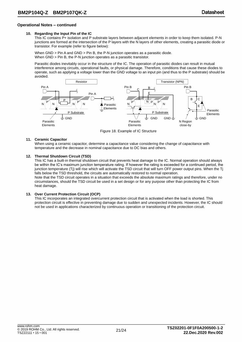
10. Regarding the Input Pin of the IC
This IC contains P+ isolation and P substrate layers between adjacent elements in order to keep them isolated. P-N junctions are formed at the intersection of the P layers with the N layers of other elements, creating a parasitic diode or transistor. For example (refer to figure below):
When GND > Pin A and GND > Pin B, the P-N junction operates as a parasitic diode. When GND > Pin B, the P-N junction operates as a parasitic transistor.
Parasitic diodes inevitably occur in the structure of the IC. The operation of parasitic diodes can result in mutual interference among circuits, operational faults, or physical damage. Therefore, conditions that cause these diodes to operate, such as applying a voltage lower than the GND voltage to an input pin (and thus to the P substrate) should be avoided.
Figure 18. Example of IC Structure
11. Ceramic Capacitor When using a ceramic capacitor, determine a capacitance value considering the change of capacitance with temperature and the decrease in nominal capacitance due to DC bias and others.
12. Thermal Shutdown Circuit (TSD)
This IC has a built-in thermal shutdown circuit that prevents heat damage to the IC. Normal operation should always be within the IC’s maximum junction temperature rating. If however the rating is exceeded for a continued period, the junction temperature (Tj) will rise which will activate the TSD circuit that will turn OFF power output pins. When the Tj falls below the TSD threshold, the circuits are automatically restored to normal operation. Note that the TSD circuit operates in a situation that exceeds the absolute maximum ratings and therefore, under no circumstances, should the TSD circuit be used in a set design or for any purpose other than protecting the IC from heat damage.
13. Over Current Protection Circuit (OCP)
This IC incorporates an integrated overcurrent protection circuit that is activated when the load is shorted. This protection circuit is effective in preventing damage due to sudden and unexpected incidents. However, the IC should not be used in applications characterized by continuous operation or transitioning of the protection circuit.
N NP
+ P
N NP
+
P Substrate
GND
NP
+
N NP
+N P
P Substrate
GND GND
Parasitic
Elements
Pin A
Pin A
Pin B Pin B
B C
E
Parasitic
Elements
GNDParasitic
Elements
CB
E
Transistor (NPN)Resistor
N Region
close-by
Parasitic
Elements
22/24
BM2P104Q-Z BM2P107QK-Z
TSZ02201-0F1F0A200500-1-2 22.Dec.2020 Rev.002
© 2019 ROHM Co., Ltd. All rights reserved. www.rohm.com
TSZ22111 • 15 • 001
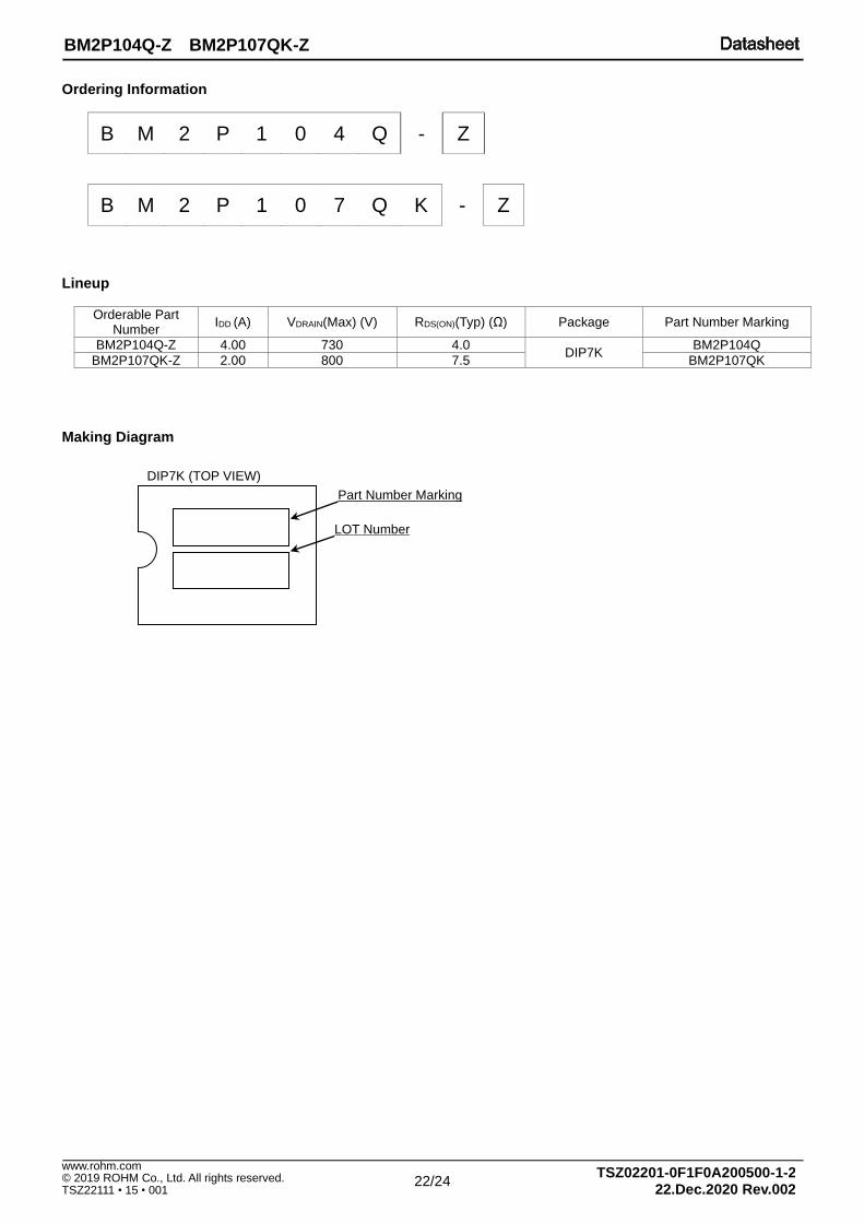
Ordering Information
B M 2 P 1 0 4 Q - Z
B M 2 P 1 0 7 Q K - Z
Lineup
Orderable Part Number
IDD (A) VDRAIN(Max) (V) RDS(ON)(Typ) (Ω) Package Part Number Marking
BM2P104Q-Z 4.00 730 4.0 DIP7K
BM2P104Q
BM2P107QK-Z 2.00 800 7.5 BM2P107QK
Making Diagram
DIP7K (TOP VIEW)
Part Number Marking
LOT Number
23/24
BM2P104Q-Z BM2P107QK-Z
TSZ02201-0F1F0A200500-1-2 22.Dec.2020 Rev.002
© 2019 ROHM Co., Ltd. All rights reserved. www.rohm.com
TSZ22111 • 15 • 001
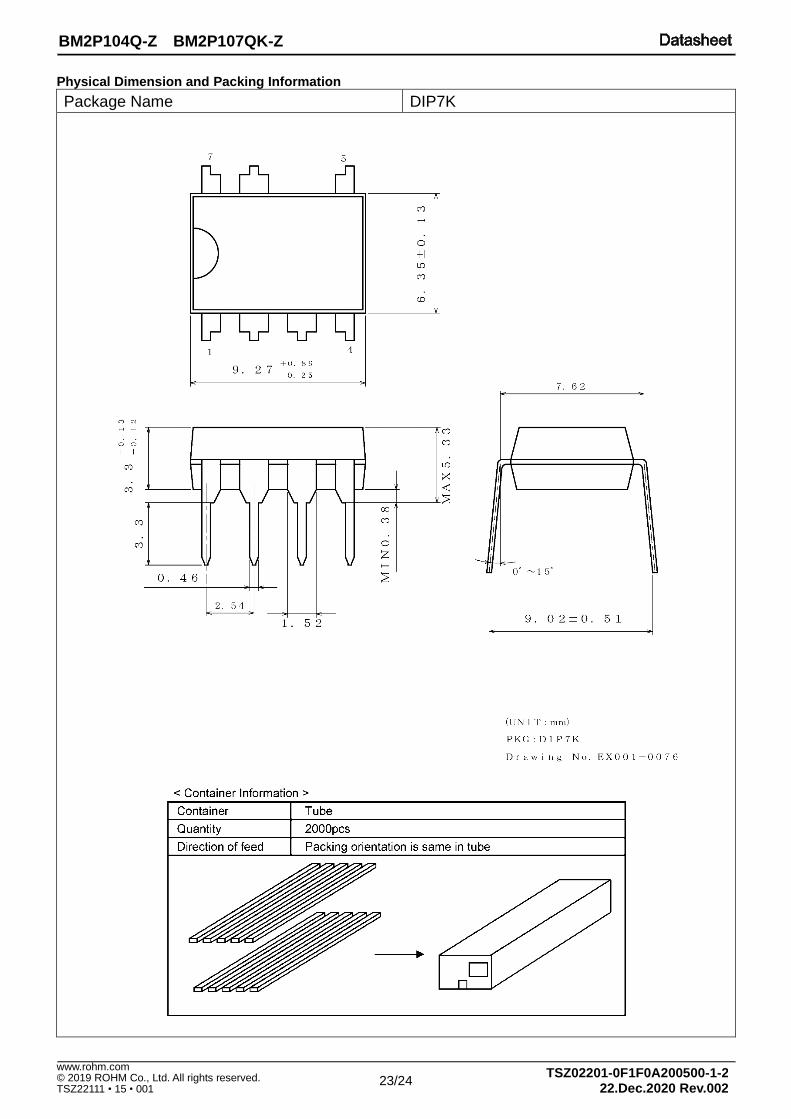
Physical Dimension and Packing Information
Package Name DIP7K

24/24
BM2P104Q-Z BM2P107QK-Z
TSZ02201-0F1F0A200500-1-2 22.Dec.2020 Rev.002
© 2019 ROHM Co., Ltd. All rights reserved. www.rohm.com
TSZ22111 • 15 • 001
Revision History
Date Revision Changes
16.Jul.2019 001 New release
22.Dec.2020 002 P15 Change the Absolute Maximum Ratings P18 Addition of the Application Examples

Notice-PGA-E Rev.004
© 2015 ROHM Co., Ltd. All rights reserved.
Notice
Precaution on using ROHM Products 1. Our Products are designed and manufactured for application in ordinary electronic equipment (such as AV equipment,
OA equipment, telecommunication equipment, home electronic appliances, amusement equipment, etc.). If youintend to use our Products in devices requiring extremely high reliability (such as medical equipment (Note 1), transportequipment, traffic equipment, aircraft/spacecraft, nuclear power controllers, fuel controllers, car equipment including caraccessories, safety devices, etc.) and whose malfunction or failure may cause loss of human life, bodily injury orserious damage to property (“Specific Applications”), please consult with the ROHM sales representative in advance.Unless otherwise agreed in writing by ROHM in advance, ROHM shall not be in any way responsible or liable for anydamages, expenses or losses incurred by you or third parties arising from the use of any ROHM’s Products for SpecificApplications.
(Note1) Medical Equipment Classification of the Specific Applications
JAPAN USA EU CHINA
CLASSⅢ CLASSⅢ
CLASSⅡb CLASSⅢ
CLASSⅣ CLASSⅢ
2. ROHM designs and manufactures its Products subject to strict quality control system. However, semiconductorproducts can fail or malfunction at a certain rate. Please be sure to implement, at your own responsibilities, adequatesafety measures including but not limited to fail-safe design against the physical injury, damage to any property, whicha failure or malfunction of our Products may cause. The following are examples of safety measures:
[a] Installation of protection circuits or other protective devices to improve system safety [b] Installation of redundant circuits to reduce the impact of single or multiple circuit failure
3. Our Products are designed and manufactured for use under standard conditions and not under any special orextraordinary environments or conditions, as exemplified below. Accordingly, ROHM shall not be in any wayresponsible or liable for any damages, expenses or losses arising from the use of any ROHM’s Products under anyspecial or extraordinary environments or conditions. If you intend to use our Products under any special orextraordinary environments or conditions (as exemplified below), your independent verification and confirmation ofproduct performance, reliability, etc, prior to use, must be necessary:
[a] Use of our Products in any types of liquid, including water, oils, chemicals, and organic solvents [b] Use of our Products outdoors or in places where the Products are exposed to direct sunlight or dust [c] Use of our Products in places where the Products are exposed to sea wind or corrosive gases, including Cl2,
H2S, NH3, SO2, and NO2
[d] Use of our Products in places where the Products are exposed to static electricity or electromagnetic waves [e] Use of our Products in proximity to heat-producing components, plastic cords, or other flammable items [f] Sealing or coating our Products with resin or other coating materials [g] Use of our Products without cleaning residue of flux (Exclude cases where no-clean type fluxes is used.
However, recommend sufficiently about the residue.) ; or Washing our Products by using water or water-soluble cleaning agents for cleaning residue after soldering
[h] Use of the Products in places subject to dew condensation
4. The Products are not subject to radiation-proof design.
5. Please verify and confirm characteristics of the final or mounted products in using the Products.
6. In particular, if a transient load (a large amount of load applied in a short period of time, such as pulse, is applied, confirmation of performance characteristics after on-board mounting is strongly recommended. Avoid applying power exceeding normal rated power; exceeding the power rating under steady-state loading condition may negatively affect product performance and reliability.
7. De-rate Power Dissipation depending on ambient temperature. When used in sealed area, confirm that it is the use inthe range that does not exceed the maximum junction temperature.
8. Confirm that operation temperature is within the specified range described in the product specification.
9. ROHM shall not be in any way responsible or liable for failure induced under deviant condition from what is defined inthis document.
Precaution for Mounting / Circuit board design 1. When a highly active halogenous (chlorine, bromine, etc.) flux is used, the residue of flux may negatively affect product
performance and reliability.
2. In principle, the reflow soldering method must be used on a surface-mount products, the flow soldering method mustbe used on a through hole mount products. If the flow soldering method is preferred on a surface-mount products,please consult with the ROHM representative in advance.
For details, please refer to ROHM Mounting specification

Notice-PGA-E Rev.004
© 2015 ROHM Co., Ltd. All rights reserved.
Precautions Regarding Application Examples and External Circuits 1. If change is made to the constant of an external circuit, please allow a sufficient margin considering variations of the
characteristics of the Products and external components, including transient characteristics, as well as static characteristics.
2. You agree that application notes, reference designs, and associated data and information contained in this document
are presented only as guidance for Products use. Therefore, in case you use such information, you are solely responsible for it and you must exercise your own independent verification and judgment in the use of such information contained in this document. ROHM shall not be in any way responsible or liable for any damages, expenses or losses incurred by you or third parties arising from the use of such information.
Precaution for Electrostatic This Product is electrostatic sensitive product, which may be damaged due to electrostatic discharge. Please take proper caution in your manufacturing process and storage so that voltage exceeding the Products maximum rating will not be applied to Products. Please take special care under dry condition (e.g. Grounding of human body / equipment / solder iron, isolation from charged objects, setting of Ionizer, friction prevention and temperature / humidity control).
Precaution for Storage / Transportation 1. Product performance and soldered connections may deteriorate if the Products are stored in the places where:
[a] the Products are exposed to sea winds or corrosive gases, including Cl2, H2S, NH3, SO2, and NO2 [b] the temperature or humidity exceeds those recommended by ROHM [c] the Products are exposed to direct sunshine or condensation [d] the Products are exposed to high Electrostatic
2. Even under ROHM recommended storage condition, solderability of products out of recommended storage time period may be degraded. It is strongly recommended to confirm solderability before using Products of which storage time is exceeding the recommended storage time period.
3. Store / transport cartons in the correct direction, which is indicated on a carton with a symbol. Otherwise bent leads
may occur due to excessive stress applied when dropping of a carton. 4. Use Products within the specified time after opening a humidity barrier bag. Baking is required before using Products of
which storage time is exceeding the recommended storage time period.
Precaution for Product Label A two-dimensional barcode printed on ROHM Products label is for ROHM’s internal use only.
Precaution for Disposition When disposing Products please dispose them properly using an authorized industry waste company.
Precaution for Foreign Exchange and Foreign Trade act Since concerned goods might be fallen under listed items of export control prescribed by Foreign exchange and Foreign trade act, please consult with ROHM in case of export.
Precaution Regarding Intellectual Property Rights 1. All information and data including but not limited to application example contained in this document is for reference
only. ROHM does not warrant that foregoing information or data will not infringe any intellectual property rights or any other rights of any third party regarding such information or data.
2. ROHM shall not have any obligations where the claims, actions or demands arising from the combination of the Products with other articles such as components, circuits, systems or external equipment (including software).
3. No license, expressly or implied, is granted hereby under any intellectual property rights or other rights of ROHM or any third parties with respect to the Products or the information contained in this document. Provided, however, that ROHM will not assert its intellectual property rights or other rights against you or your customers to the extent necessary to manufacture or sell products containing the Products, subject to the terms and conditions herein.
Other Precaution 1. This document may not be reprinted or reproduced, in whole or in part, without prior written consent of ROHM.
2. The Products may not be disassembled, converted, modified, reproduced or otherwise changed without prior written consent of ROHM.
3. In no event shall you use in any way whatsoever the Products and the related technical information contained in the Products or this document for any military purposes, including but not limited to, the development of mass-destruction weapons.
4. The proper names of companies or products described in this document are trademarks or registered trademarks of ROHM, its affiliated companies or third parties.

DatasheetDatasheet
Notice – WE Rev.001© 2015 ROHM Co., Ltd. All rights reserved.
General Precaution 1. Before you use our Products, you are requested to carefully read this document and fully understand its contents.
ROHM shall not be in any way responsible or liable for failure, malfunction or accident arising from the use of any ROHM’s Products against warning, caution or note contained in this document.
2. All information contained in this document is current as of the issuing date and subject to change without any prior
notice. Before purchasing or using ROHM’s Products, please confirm the latest information with a ROHM sales representative.
3. The information contained in this document is provided on an “as is” basis and ROHM does not warrant that all
information contained in this document is accurate and/or error-free. ROHM shall not be in any way responsible or liable for any damages, expenses or losses incurred by you or third parties resulting from inaccuracy or errors of or concerning such information.