Embed Size (px)
Citation preview
Modeling, Simulation and Design of Input Filter for Matrix Converters
ADRIAN POPOVICI, VIOREL POPESCU, MIRCEA BABAITA, DAN LASCU, DAN NEGOITESCU Applied Electronics Department
Politehnica University of Timisoara Address Bd. Vasile Parvan No.2
ROMANIA
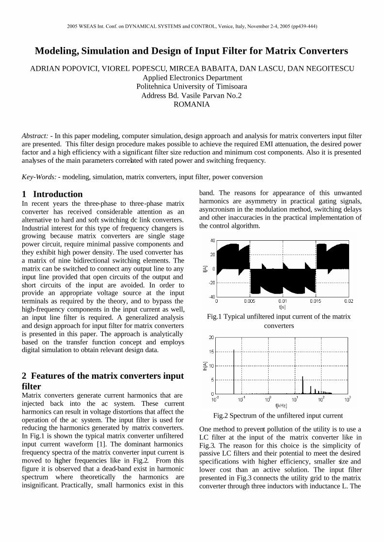
Abstract: - In this paper modeling, computer simulation, design approach and analysis for matrix converters input filter are presented. This filter design procedure makes possible to achieve the required EMI attenuation, the desired power factor and a high efficiency with a significant filter size reduction and minimum cost components. Also it is presented analyses of the main parameters correlated with rated power and switching frequency. Key-Words: - modeling, simulation, matrix converters, input filter, power conversion 1 Introduction In recent years the three-phase to three-phase matrix converter has received considerable attention as an alternative to hard and soft switching dc link converters. Industrial interest for this type of frequency changers is growing because matrix converters are single stage power circuit, require minimal passive components and they exhibit high power density. The used converter has a matrix of nine bidirectional switching elements. The matrix can be switched to connect any output line to any input line provided that open circuits of the output and short circuits of the input are avoided. In order to provide an appropriate voltage source at the input terminals as required by the theory, and to bypass the high-frequency components in the input current as well, an input line filter is required. A generalized analysis and design approach for input filter for matrix converters is presented in this paper. The approach is analytically based on the transfer function concept and employs digital simulation to obtain relevant design data. 2 Features of the matrix converters input filter Matrix converters generate current harmonics that are injected back into the ac system. These current harmonics can result in voltage distortions that affect the operation of the ac system. The input filter is used for reducing the harmonics generated by matrix converters. In Fig.1 is shown the typical matrix converter unfiltered input current waveform [1]. The dominant harmonics frequency spectra of the matrix converter input current is moved to higher frequencies like in Fig.2. From this figure it is observed that a dead-band exist in harmonic spectrum where theoretically the harmonics are insignificant. Practically, small harmonics exist in this
band. The reasons for appearance of this unwanted harmonics are asymmetry in practical gating signals, asyncronism in the modulation method, switching delays and other inaccuracies in the practical implementation of the control algorithm.
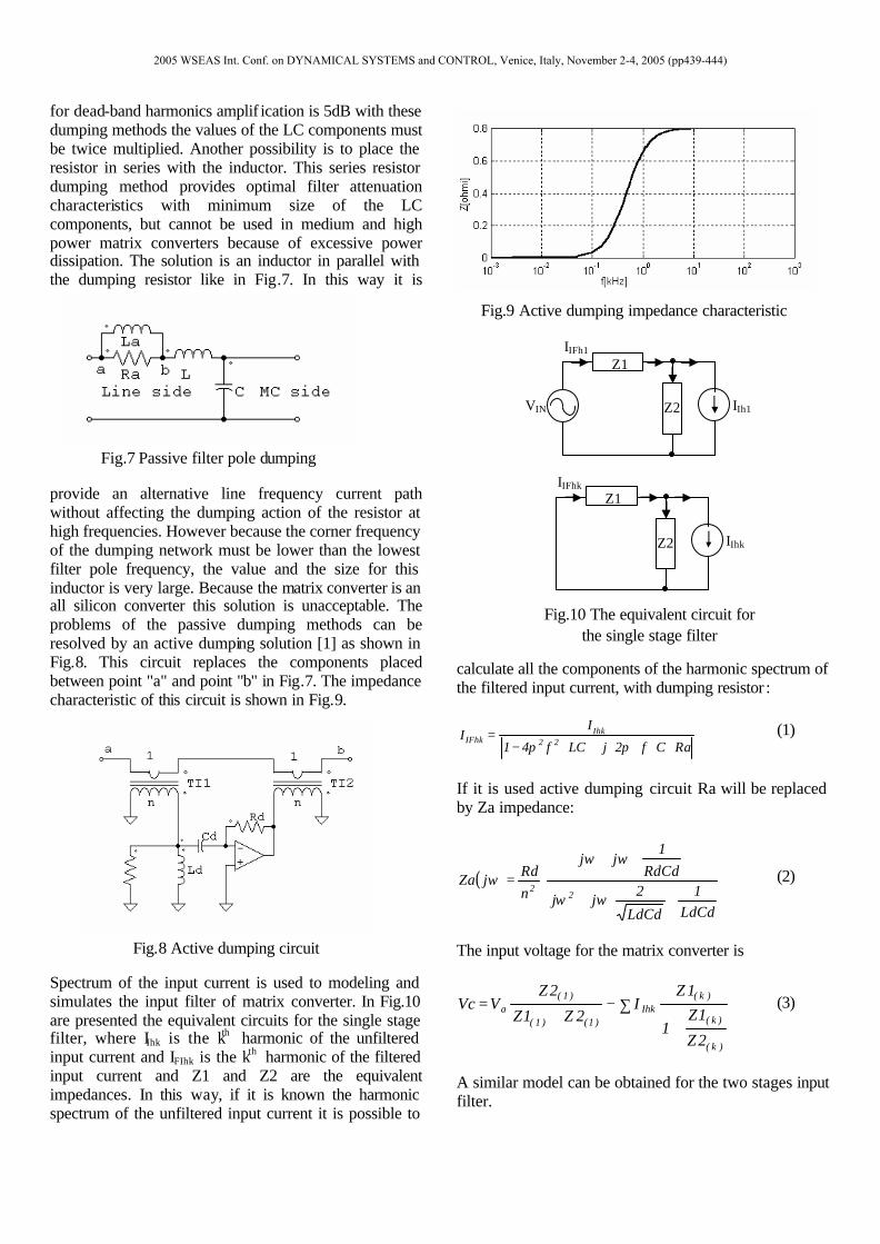
One method to prevent pollution of the utility is to use a LC filter at the input of the matrix converter like in Fig.3. The reason for this choice is the simplicity of passive LC filters and their potential to meet the desired specifications with higher efficiency, smaller size and lower cost than an active solution. The input filter presented in Fig.3 connects the utility grid to the matrix converter through three inductors with inductance L. The
Fig.1 Typical unfiltered input current of the matrix converters
Fig.2 Spectrum of the unfiltered input current
2005 WSEAS Int. Conf. on DYNAMICAL SYSTEMS and CONTROL, Venice, Italy, November 2-4, 2005 (pp439-444)
capacitors C provide a low impedance path for the high frequency ripple current and thus attenuate the content of current ripple in the utility current. The filter capacitors are Y-connected to a virtual neutral point so that it is reduced the voltage rating of the capacitors.
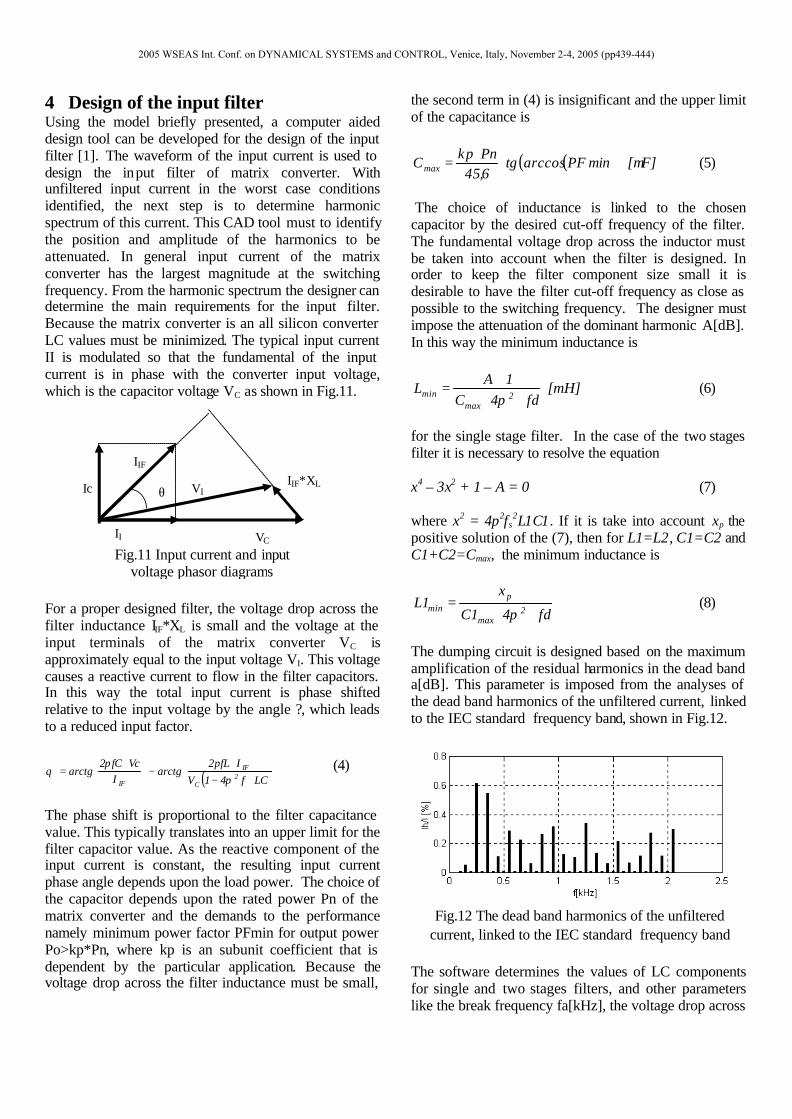
The main requirements an input filter has to meet are the following: required switching noise attenuation, keeping the input voltage from changing significantly during each PWM cycle, low input displacement angle between filter input voltage and current and overall system stability [2]. Other practical consideration for designer are the tolerances on the value of the filter components, the effect of the filter on the matrix converter performance and on the rating of the converter components, consideration related to system efficiency, cost of the filter [3]. Also the input filter distorts the converter input voltage like in Fig.4, and this additional distortion must be considered in the filter design.
3 Modeling Input Filter For the filter modeling and design a single phase equivalent of the filter configuration is used like in Fig.5. A single stage LC filter could be used in many cases. However in the light of the new harmonic and EMI reduction standards to meet the required attenuation a single stage filter can become large. For example EMI control standard CISPR11[4] states the frequency range
between 150 KHz and 3 MHz. This standard also states that the frequency range 10KHz to 150KHz is under review. Another important standard are IEC 1000-3-2 [5] document for equipment with rated current less than 16A and IEC 1000-3-4 [6] document for equipment with rated current greater than 16A. These standards specify the harmonic content of the line current up to the 39th harmonic. The future viability of the matrix converters may depend on the effects any future legislation in this area has on the input filter requirements. Other solutions are to use a two stages filter like in Fig.6 or a single stage filter with a tuned harmonic diversion [3]. The use of tuned filters necessitates the use of components with good tolerance and stability so that this is a high cost solution.. For this reason this paper is focused on approach design for single stage and two stages LC filters.
In order to avoid amplification of the residual harmonics in the dead-band region damping of the LC filter is required. It has been shown if the amplitude of the residual harmonics is less one percent an amplification of maximum 15dB can be tolerated. However the harmonics limits imposed by IEC 1000-3-2 and IEC 1000-3-4 standards for high frequency switching matrix converters are in the dead band of the input current spectra. In some cases only amplification less than 3dB can meet these standards specifications [3]. Proper filter pole dumping is important for achieving low filter output impedance for all frequencies and thus overall system stability and for avoiding amplification of the residual harmonics in the dead band. Usually, a resistor is used for filter pole dumping. For single stage LC filter the resistor may be in parallel with the inductors or in series with the capacitor. These resistor locations provide minimal dissipation in the filter. However in order for the dumping resistor to be effective the LC components have to be oversized. For example if the maximum limit
Fig.3 Structure of the matrix converter
Fig.6 Two stages input filter
Fig.4 Distorted input voltage waveform
Fig.5 Single stage input filter
2005 WSEAS Int. Conf. on DYNAMICAL SYSTEMS and CONTROL, Venice, Italy, November 2-4, 2005 (pp439-444)
for dead-band harmonics amplif ication is 5dB with these dumping methods the values of the LC components must be twice multiplied. Another possibility is to place the resistor in series with the inductor. This series resistor dumping method provides optimal filter attenuation characteristics with minimum size of the LC components, but cannot be used in medium and high power matrix converters because of excessive power dissipation. The solution is an inductor in parallel with the dumping resistor like in Fig.7. In this way it is
provide an alternative line frequency current path without affecting the dumping action of the resistor at high frequencies. However because the corner frequency of the dumping network must be lower than the lowest filter pole frequency, the value and the size for this inductor is very large. Because the matrix converter is an all silicon converter this solution is unacceptable. The problems of the passive dumping methods can be resolved by an active dumping solution [1] as shown in Fig.8. This circuit replaces the components placed between point "a" and point "b" in Fig.7. The impedance characteristic of this circuit is shown in Fig.9.
Spectrum of the input current is used to modeling and simulates the input filter of matrix converter. In Fig.10 are presented the equivalent circuits for the single stage filter, where IIhk is the kth harmonic of the unfiltered input current and IFIhk is the kth harmonic of the filtered input current and Z1 and Z2 are the equivalent impedances. In this way, if it is known the harmonic spectrum of the unfiltered input current it is possible to
calculate all the components of the harmonic spectrum of the filtered input current, with dumping resistor :
RaCf2jLCf41
II
22Ihk
IFhk⋅⋅⋅⋅+⋅−
=ππ
(1)
If it is used active dumping circuit Ra will be replaced by Za impedance:
( )
LdCd1
LdCd
2jj
RdCd1
jj
nRdjZa
22
+⋅+
+⋅
⋅=ωω
ωωω (2)
The input voltage for the matrix converter is
∑+
−+
=
)k(
)k(
)k(Ihk
)1()1(
)1(a
2Z
1Z1
1ZI
2Z1Z
2ZVVc (3)
A similar model can be obtained for the two stages input filter.
Fig.7 Passive filter pole dumping
Fig.8 Active dumping circuit
Fig.9 Active dumping impedance characteristic
Z2
Z1
IIhk
IIFhk
Z2
Z1
IIh1
IIFh1
VIN
Fig.10 The equivalent circuit for the single stage filter
2005 WSEAS Int. Conf. on DYNAMICAL SYSTEMS and CONTROL, Venice, Italy, November 2-4, 2005 (pp439-444)
4 Design of the input filter Using the model briefly presented, a computer aided design tool can be developed for the design of the input filter [1]. The waveform of the input current is used to design the input filter of matrix converter. With unfiltered input current in the worst case conditions identified, the next step is to determine harmonic spectrum of this current. This CAD tool must to identify the position and amplitude of the harmonics to be attenuated. In general input current of the matrix converter has the largest magnitude at the switching frequency. From the harmonic spectrum the designer can determine the main requirements for the input filter. Because the matrix converter is an all silicon converter LC values must be minimized. The typical input current II is modulated so that the fundamental of the input current is in phase with the converter input voltage, which is the capacitor voltage VC as shown in Fig.11.
For a proper designed filter, the voltage drop across the filter inductance IIF*XL is small and the voltage at the input terminals of the matrix converter VC is approximately equal to the input voltage VI. This voltage causes a reactive current to flow in the filter capacitors. In this way the total input current is phase shifted relative to the input voltage by the angle ?, which leads to a reduced input factor.
( )
⋅−⋅
−
⋅=
LCf41VIfL2
arctgI
VcfC2arctg 2
C
IF
IF πππ
θ (4)
The phase shift is proportional to the filter capacitance value. This typically translates into an upper limit for the filter capacitor value. As the reactive component of the input current is constant, the resulting input current phase angle depends upon the load power. The choice of the capacitor depends upon the rated power Pn of the matrix converter and the demands to the performance namely minimum power factor PFmin for output power Po>kp*Pn, where kp is an subunit coefficient that is dependent by the particular application. Because the voltage drop across the filter inductance must be small,
the second term in (4) is insignificant and the upper limit of the capacitance is
( )( )minPFarccostg6,45Pnkp
Cmax ⋅⋅
= [µF] (5)
The choice of inductance is linked to the chosen capacitor by the desired cut-off frequency of the filter. The fundamental voltage drop across the inductor must be taken into account when the filter is designed. In order to keep the filter component size small it is desirable to have the filter cut-off frequency as close as possible to the switching frequency. The designer must impose the attenuation of the dominant harmonic A[dB]. In this way the minimum inductance is
fd4C1A
L2
maxmin ⋅⋅
+=
π [mH] (6)
for the single stage filter. In the case of the two stages filter it is necessary to resolve the equation x4 – 3x2 + 1 – A = 0 (7) where x2 = 4p2fs
2L1C1. If it is take into account xp the positive solution of the (7), then for L1=L2, C1=C2 and C1+C2=Cmax, the minimum inductance is
fd41C
x1L
2max
pmin ⋅⋅
=π
(8)
The dumping circuit is designed based on the maximum amplification of the residual harmonics in the dead band a[dB]. This parameter is imposed from the analyses of the dead band harmonics of the unfiltered current, linked to the IEC standard frequency band, shown in Fig.12.
The software determines the values of LC components for single and two stages filters, and other parameters like the break frequency fa[kHz], the voltage drop across
VC II
Ic VI
IIF
IIF*XL θ
Fig.11 Input current and input voltage phasor diagrams
Fig.12 The dead band harmonics of the unfiltered current, linked to the IEC standard frequency band
2005 WSEAS Int. Conf. on DYNAMICAL SYSTEMS and CONTROL, Venice, Italy, November 2-4, 2005 (pp439-444)
the filter inductance u[%] and the relative cost factor $[p.u] [1] [3]. The cost factor can be used to optimize the relative proportions of the inductance and capacitance in the matrix converter input filter. The design procedure is extensive presented in [1]. For example in Fig.13 are shown attenuation characteristics of the single and two input filters, regarding to the Fig.1 unfiltered input current waveform. The control algorithm is one of the more used, the space vector modulation [1]. The total harmonic distortion factor is THD=73,76% for this unfiltered current. In this case the input design parameters are: the rated power is Pn=10kW, the minimum power factor PFmin=0.9, the coefficient kp=10%, the switching frequency and the dominant harmonic frequency are fd=20kHz, the required attenuation of the dominant harmonic is A=30dB and the maximum amplification of the residual harmonics in the dead band a=3dB. The input filter parameters are C=10,87µF, L=0,109mH, Ra=0,802O for the single stage filter, and C1=C2=5,44µF, L1=L2=0,068mH, Ra=1,703 O for two stages filter.
Because IEC 1000-3-2 or IEC 1000-3-4 standards requirements must be achieved, an useful feature of the computer aided design tool is the possibility to display harmonic spectrum of the filtered input current and the IEC 1000-3-2 or IEC 1000-3-4 limits, symbols "*" in Fig.14.
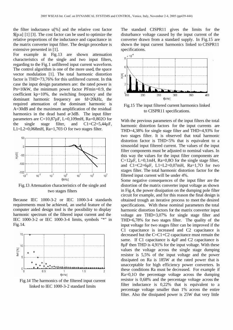
The standard CISPR11 gives the limits for the disturbance voltage caused by the input current of the converter drawn from a standard supply. In Fig.15 are shown the input current harmonics linked to CISPR11 specifications.
With the previous parameters of the input filters the total harmonic distortion factors for the input currents are THD=4,38% for single stage filter and THD=4,93% for two stages filter. It is observed that total harmonic distortion factor is THD<5% that is equivalent to a sinusoidal input filtered current. The values of the input filter components must be adjusted to nominal values. In this way the values for the input filter components are C=12µF, L=0,1mH, Ra=0,8O for the single stage filter, and C1=C2=6µF, L1=L2=0,07mH, Ra=1,7O for two stages filter. The total harmonic distortion factor for the filtered input current will be under 4%. Some negative consequences of the input filter are the distortion of the matrix converter input voltage as shown in Fig.4, the power dissipation on the dumping pole filter circuit for example, and for this reason the final design is obtained trough an iterative process to meet the desired specifications. With these nominal parameters the total harmonic distortion factors for the matrix converter input voltage are THD=3,07% for single stage filter and THD=6,78% for two stages filter. The quality of the input voltage for two stages filter can be improved if the C1 capacitance is increased and C2 capacitance is decreased but the C=C1+C2 capacitance must remain the same. If C1 capacitance is 4µF and C2 capacitance is 8µF then THD is 4,91% for the input voltage. With these values the voltage across the single stage dumping resistor is 5,5% of the input voltage and the power dissipated on Ra is 185W at the rated power that is unacceptable for high efficiency power converters. In these conditions Ra must be decreased. For example if Ra=0,1O the percentage voltage across the dumping resistor is 0,68% and the percentage voltage across the filter inductance is 0,22% that is equivalent to a percentage voltage smaller than 1% across the entire filter. Also the dissipated power is 25W that very little
Fig.13 Attenuation characteristics of the single and two stages filters
Fig.14 The harmonics of the filtered input current linked to IEC 1000-3-2 standard limits
Fig.15 The input filtered current harmonics linked to CISPR11 specifications.
2005 WSEAS Int. Conf. on DYNAMICAL SYSTEMS and CONTROL, Venice, Italy, November 2-4, 2005 (pp439-444)
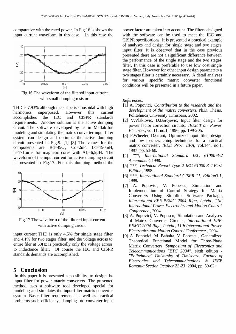
comparative with the rated power. In Fig.16 is shown the input current waveform in this case. In this case the
THD is 7,93% although the shape is sinusoidal with high harmonics superposed. However this current accomplishes the IEC and CISPR standards requirements. Another solution is the active dumping circuit. The software developed by us in Matlab for modeling and simulating the matrix converter input filter system can design and optimize the active dumping circuit presented in Fig.9. [1] [8] The values for the components are Rd=49O, Cd=2uF, Ld=190mH, n=171turns for magnetic cores with AL=6,5µH. The waveform of the input current for active dumping circuit is presented in Fig.17. For this dumping method the
input current THD is only 4,5% for single stage filter and 4,1% for two stages filter and the voltage across to entire filer at 50Hz is practically only the voltage across to inductance filter. Of course the IEC and CISPR standards demands are accomplished. 5 Conclusion In this paper it is presented a possibility to design the input filter for power matrix converters. The presented method uses a software tool developed special for modeling and simulates the input filter matrix converter system. Basic filter requirements as well as practical problems such efficiency, damping and converter input
power factor are taken into account. The filters designed with the software can be used to meet the IEC and CISPR specifications. It is presented a practical example of analyses and design for single stage and two stages input filter. It is observed that in the case previous presented there are not a significant difference between the performance of the single stage and the two stages filter. In this case is preferable to use low cost single stage filter. However for other input design parameters a two stages filter is certainly necessary. A detail analyses for various specific matrix converter functional conditions will be presented in a future paper. References: [1] A. Popovici, Contribution to the research and the
development of the matrix converters, Ph.D. Thesis, Politehnica University Timisoara, 2002.
[2] V.Vlaktovic, D.Borojevic, Input filter design for power factor correction circuits, IEEE Tran. Power Electron., vol.11, no.1, 1996, pp. 199-205.
[3] P.Wheeler, D.Grant, Optimized input filter design and low loss switching techniques for a practical matrix converter, IEEE Proc. EPA, vol.144, no.1, 1997 pp. 53-60.
[4] ***, International Standard IEC 61000-3-2 Amendment, 1998.
[5] ***, Technical Report Type 2 IEC 61000-3-4 First Edition, 1998.
[6] ***, International Standard CISPR 11, Edition3.1, 1999.
[7] A. Popovici, V. Popescu, Simulation and Implementation of Control Strategy for Matrix Converters Using Simulink Software Package, International EPE-PEMC 2004 Riga, Latvia , 11th International Power Electronics and Motion Control Conference , 2004.
[8] A. Popovici, V. Popescu, Simulation and Analyses of Matrix Converter Circuits, International EPE-PEMC 2004 Riga, Latvia , 11th International Power Electronics and Motion Control Conference , 2004.
[9] A. Popovici, M. Babaita, V. Popescu, Generalized Theoretical Functional Model for Three-Phase Matrix Converters, Symposium of Electronics and Telecommunications "ETC 2004", sixth edition -"Politehnica" University of Timisoara, Faculty of Electronics and Telecommunications & IEEE Romania Section October 22-23, 2004, pp. 59-62.
Fig.17 The waveform of the filtered input current with active dumping circuit
Fig.16 The waveform of the filtered input current with small dumping resistor
2005 WSEAS Int. Conf. on DYNAMICAL SYSTEMS and CONTROL, Venice, Italy, November 2-4, 2005 (pp439-444)