Embed Size (px)
Citation preview
GigaDevice Semiconductor Inc.
GD32E103xx
Arm® Cortex®-M4 32-bit MCU
Datasheet
GD32E103xx Datasheet
1
Table of Contents
Table of Contents ........................................................................................................... 1
List of Figures ................................................................................................................ 4
List of Tables .................................................................................................................. 5
1. General description ................................................................................................. 7
2. Device overview ....................................................................................................... 8
2.1. Device information ...................................................................................................... 8
2.2. Block diagram .............................................................................................................. 9
2.3. Pinouts and pin assignment ..................................................................................... 10
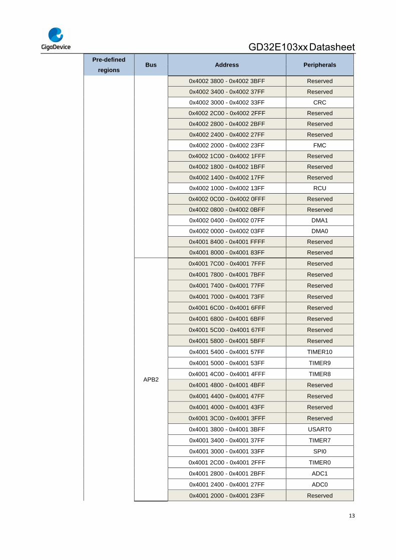
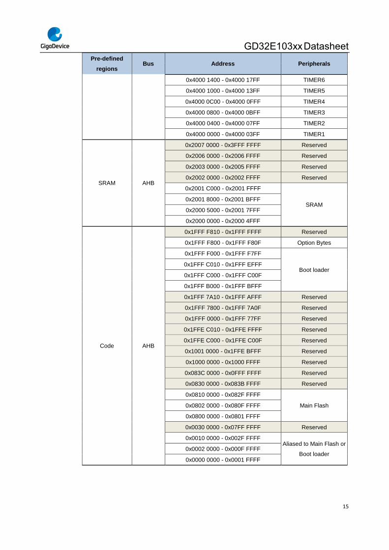
2.4. Memory map .............................................................................................................. 12
2.5. Clock tree ................................................................................................................... 16
2.6. Pin definitions ............................................................................................................ 16
2.6.1. GD32E103Vx LQFP100 pin definitions ................................................................................ 17
2.6.2. GD32E103Rx LQFP64 pin definitions .................................................................................. 23
2.6.3. GD32E103Cx LQFP48 pin definitions .................................................................................. 27
2.6.4. GD32E103Tx QFN36 pin definitions .................................................................................... 30
3. Functional description .......................................................................................... 33
3.1. Arm® Cortex®-M4 core ............................................................................................... 33
3.2. On-chip memory ........................................................................................................ 33
3.3. Clock, reset and supply management ...................................................................... 34
3.4. Boot modes ................................................................................................................ 34
3.5. Power saving modes ................................................................................................. 35
3.6. Analog to digital converter (ADC) ............................................................................ 35
3.7. Digital to analog converter (DAC) ............................................................................. 36
3.8. DMA ............................................................................................................................ 36
3.9. General-purpose inputs/outputs (GPIOs) ................................................................ 36
3.10. Timers and PWM generation ................................................................................. 37
3.11. Real time clock (RTC) ............................................................................................ 38
3.12. Inter-integrated circuit (I2C) .................................................................................. 38
3.13. Serial peripheral interface (SPI) ............................................................................ 38
3.14. Universal synchronous asynchronous receiver transmitter (USART) ............... 39
GD32E103xx Datasheet
2
3.15. Inter-IC sound (I2S) ................................................................................................ 39
3.16. Universal serial bus full-speed interface (USBFS) ............................................... 39
3.17. External memory controller (EXMC) ..................................................................... 40
3.18. Debug mode ........................................................................................................... 40
3.19. Package and operation temperature ..................................................................... 40
4. Electrical characteristics ....................................................................................... 41
4.1. Absolute maximum ratings ....................................................................................... 41
4.2. Operating conditions characteristics ....................................................................... 41
4.3. Power consumption .................................................................................................. 43
4.4. EMC characteristics .................................................................................................. 50
4.5. Power supply supervisor characteristics ................................................................ 50
4.6. Electrical sensitivity .................................................................................................. 51
4.7. External clock characteristics .................................................................................. 52
4.8. Internal clock characteristics ................................................................................... 54
4.9. PLL characteristics.................................................................................................... 55
4.10. Memory characteristics ......................................................................................... 56
4.11. NRST pin characteristics ....................................................................................... 56
4.12. GPIO characteristics .............................................................................................. 57
4.13. ADC characteristics ............................................................................................... 59
4.14. Temperature sensor characteristics ..................................................................... 60
4.15. DAC characteristics ............................................................................................... 60
4.16. I2C characteristics ................................................................................................. 62
4.17. SPI characteristics ................................................................................................. 62
4.18. I2S characteristics.................................................................................................. 64
4.19. USART characteristics ........................................................................................... 66
4.20. USBFS characteristics ........................................................................................... 66
4.21. EXMC characteristics ............................................................................................. 67
4.22. TIMER characteristics ............................................................................................ 71
4.23. WDGT characteristics ............................................................................................ 71
4.24. Parameter conditions ............................................................................................. 72
5. Package information .............................................................................................. 73
5.1. LQFP100 package outline dimensions ..................................................................... 73
GD32E103xx Datasheet
3
5.2. LQFP64 package outline dimensions....................................................................... 75
5.3. LQFP48 package outline dimensions....................................................................... 77
5.4. QFN36 package outline dimensions ........................................................................ 79
5.5. Thermal characteristics ............................................................................................ 81
6. Ordering information ............................................................................................. 83
7. Revision history ..................................................................................................... 84
GD32E103xx Datasheet
4
List of Figures
Figure 2-1.GD32E103xx block diagram ..................................................................................................... 9
Figure 2-2. GD32E103Vx LQFP100 pinouts ............................................................................................ 10
Figure 2-3. GD32E103Rx LQFP64 pinouts ............................................................................................... 11
Figure 2-4. GD32E103Cx LQFP48 pinouts ............................................................................................... 11
Figure 2-5. GD32E103Tx QFN36 pinouts ................................................................................................. 12
Figure 2-6. GD32E103xx clock tree .......................................................................................................... 16
Figure 4-1. Recommended power supply decoupling capacitors(1)(2) .................................................. 41
Figure 4-2. Typical supply current consumption in Run mode ............................................................ 48
Figure 4-3. Typical supply current consumption in Sleep mode .......................................................... 48
Figure 4-4. Recommended external NRST pin circuit............................................................................ 57
Figure 4-5. I/O port AC characteristics definition ................................................................................... 58
Figure 4-6. I2C bus timing diagram.......................................................................................................... 62
Figure 4-7. SPI timing diagram - master mode ....................................................................................... 63
Figure 4-8. SPI timing diagram - slave mode .......................................................................................... 64
Figure 4-9. I2S timing diagram - master mode ....................................................................................... 65
Figure 4-10. I2S timing diagram - slave mode ........................................................................................ 66
Figure 4-11. USBFS timings: definition of data signal rise and fall time ............................................. 67
Figure 5-1. LQFP100 package outline ..................................................................................................... 73
Figure 5-2. LQFP100 recommended footprint ........................................................................................ 74
Figure 5-3. LQFP64 package outline ....................................................................................................... 75
Figure 5-4. LQFP64 recommended footprint .......................................................................................... 76
Figure 5-5. LQFP48 package outline ....................................................................................................... 77
Figure 5-6. LQFP48 recommended footprint .......................................................................................... 78
Figure 5-7. QFN36 package outline ......................................................................................................... 79
Figure 5-8. QFN36 recommended footprint ............................................................................................ 80
GD32E103xx Datasheet
5
List of Tables
Table 2-1. GD32E103xx devices features and peripheral list .................................................................. 8
Table 2-2. GD32E103xx memory map ...................................................................................................... 12
Table 2-3. GD32E103Vx LQFP100 pin definitions ................................................................................... 17
Table 2-4. GD32E103Rx LQFP64 pin definitions .................................................................................... 23
Table 2-5. GD32E103Cx LQFP48 pin definitions .................................................................................... 27
Table 2-6. GD32E103Tx LQFP36 pin definitions ..................................................................................... 30
Table 4-1. Absolute maximum ratings(1)(4) ............................................................................................... 41
Table 4-2. DC operating conditions ......................................................................................................... 41
Table 4-3. Clock frequency(1) .................................................................................................................... 42
Table 4-4. Operating conditions at Power up/ Power down(1) ............................................................... 42
Table 4-5. Start-up timings of Operating conditions(1)(2)(3) ..................................................................... 42
Table 4-6. Power saving mode wakeup timings characteristics(1)(2) ..................................................... 42
Table 4-7. Power consumption characteristics(2)(3)(4)(5) .......................................................................... 43
Table 4-8. Peripheral current consumption characteristics(1) ............................................................... 48
Table 4-9. EMS characteristics(1) .............................................................................................................. 50
Table 4-10. Power supply supervisor characteristics............................................................................ 50
Table 4-11. ESD characteristics(1) ............................................................................................................ 51
Table 4-12. Static latch-up characteristics(1) ........................................................................................... 52
Table 4-13. High speed external clock (HXTAL) generated from a crystal/ceramic characteristics . 52
Table 4-14. High speed external clock characteristics (HXTAL in bypass mode) .............................. 52
Table 4-15. Low speed external clock (LXTAL) generated from a crystal/ceramic characteristics .. 53
Table 4-16.Low speed external user clock characteristics (LXTAL in bypass mode)........................ 53
Table 4-17. High speed internal clock (IRC8M) characteristics ............................................................ 54
Table 4-18. Low speed internal clock (IRC40K) characteristics ........................................................... 54
Table 4-19. High speed internal clock (IRC48M) characteristics .......................................................... 55
Table 4-20. PLL characteristics ................................................................................................................ 55
Table 4-21. PLL1/2 characteristics ........................................................................................................... 55
Table 4-22. Flash memory characteristics .............................................................................................. 56
Table 4-23. NRST pin characteristics ...................................................................................................... 56
Table 4-24. I/O port DC characteristics(1)(3) .............................................................................................. 57
Table 4-25. I/O port AC characteristics(1)(2) .............................................................................................. 58
Table 4-26. ADC characteristics ............................................................................................................... 59
Table 4-27. ADC RAIN max for fADC = 42 MHz ............................................................................................ 59
Table 4-28. ADC dynamic accuracy at fADC = 14 MHz(1) .......................................................................... 60
Table 4-29. ADC dynamic accuracy at fADC = 42 MHz(1) .......................................................................... 60
Table 4-30. ADC static accuracy at fADC = 42 MHz(1) ............................................................................... 60
Table 4-31. Temperature sensor characteristics(1) ................................................................................. 60
Table 4-32. DAC characteristics ............................................................................................................... 60
Table 4-33. I2C characteristics(1)(2) ........................................................................................................... 62
Table 4-34. Standard SPI characteristics(1) ............................................................................................. 62
GD32E103xx Datasheet
6
Table 4-35. I2S characteristics(1)(2) ........................................................................................................... 64
Table 4-36. USART characteristics(1) ....................................................................................................... 66
Table 4-37. USBFS start up time .............................................................................................................. 66
Table 4-38. USBFS DC electrical characteristics ................................................................................... 66
Table 4-39. USBFS electrical characteristics(1) ....................................................................................... 67
Table 4-40. Asynchronous non-multiplexed SRAM/PSRAM/NOR read timings(1)(2)(3) ......................... 67
Table 4-41. Asynchronous non-multiplexed SRAM/PSRAM/NOR write timings(1)(2)(3) ........................ 68
Table 4-42. Asynchronous multiplexed PSRAM/NOR read timings(1)(2)(3) ............................................ 68
Table 4-43. Asynchronous multiplexed PSRAM/NOR write timings(1)(2)(3)............................................ 69
Table 4-44. Synchronous multiplexed PSRAM/NOR read timings(1)(2)(3)............................................... 69
Table 4-45. Synchronous multiplexed PSRAM write timings(1)(2)(3) ....................................................... 69
Table 4-46. Synchronous non-multiplexed PSRAM/NOR read timings(1)(2)(3) ....................................... 70
Table 4-47. Synchronous non-multiplexed PSRAM write timings(1)(2)(3) ............................................... 70
Table 4-48. TIMER characteristics(1) ........................................................................................................ 71
Table 4-49. FWDGT min/max timeout period at 40 kHz (IRC40K)(1) ...................................................... 71
Table 4-50. WWDGT min-max timeout value at 60 MHz (fPCLK1)(1).......................................................... 71
Table 5-1. LQFP100 package dimensions ............................................................................................... 73
Table 5-2. LQFP64 package dimensions ................................................................................................. 75
Table 5-3. LQFP48 package dimensions ................................................................................................. 77
Table 5-4. QFN36 package dimensions ................................................................................................... 79
Table 5-5. Package thermal characteristics(1) ......................................................................................... 81
Table 6-1. Part ordering code for GD32E103xx devices ........................................................................ 83
Table 7-1. Revision history ....................................................................................................................... 84
GD32E103xx Datasheet
7
1. General description
The GD32E103xx device belongs to the connectivity line of GD32 MCU Family. It is a 32-bit
general-purpose microcontroller based on the Arm® Cortex®-M4 RISC core with best cost-
performance ratio in terms of enhanced processing capacity, reduced power consumption
and peripheral set. The Cortex®-M4 core features implements a full set of DSP instructions to
address digital signal control markets that demand an efficient, easy-to-use blend of control
and signal processing capabilities. It also provides powerful trace technology for enhanced
application security and advanced debug support.
The GD32E103xx device incorporates the Arm® Cortex®-M4 32-bit processor core operating
at 120 MHz frequency with Flash accesses to obtain maximum efficiency. It provides up to
128 KB on-chip Flash memory and 32 KB SRAM memory. An extensive range of enhanced
I/Os and peripherals connected to two APB buses. The devices offer up to two 12-bit 3 MSPS
ADCs, two 12-bit DACs, up to ten general 16-bit timers, two 16-bit PWM advanced timers,
and two 16-bit basic timers, as well as standard and advanced communication interfaces: up
to three SPIs, two I2Cs, three USARTs and two UARTs, two I2Ss and an USBFS.
The device operates from 1.71 to 3.6 V power supply and available in –40 to +85 °C
temperature range. Several power saving modes provide the flexibility for maximum
optimization between wakeup latency and power consumption, an especially important
consideration in low power applications.
The above features make GD32E103xx devices suitable for a wide range of interconnection
and advanced applications, especially in areas such as industrial control, motor drives,
consumer and handheld equipment, human machine interface, security and alarm systems,
POS, automotive navigation, IoT and so on.
GD32E103xx Datasheet
8
2. Device overview
2.1. Device information
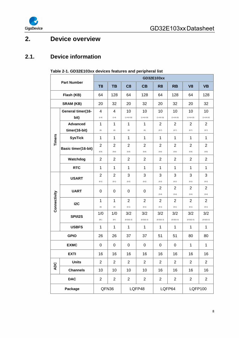
Table 2-1. GD32E103xx devices features and peripheral list
Part Number
GD32E103xx
T8 TB C8 CB R8 RB V8 VB
Flash (KB) 64 128 64 128 64 128 64 128
SRAM (KB) 20 32 20 32 20 32 20 32
Tim
ers
General timer(16-
bit)
4
(1-4)
4
(1-4)
10
(1-4,8-13)
10
(1-4,8-13)
10
(1-4,8-13)
10
(1-4,8-13)
10
(1-4,8-13)
10
(1-4,8-13)
Advanced
timer(16-bit)
1
(0)
1
(0)
1
(0)
1
(0)
2
(0,7)
2
(0,7)
2
(0,7)
2
(0,7)
SysTick 1 1 1 1 1 1 1 1
Basic timer(16-bit) 2
(5,6)
2
(5,6)
2
(5,6)
2
(5,6)
2
(5,6)
2
(5,6)
2
(5,6)
2
(5,6)
Watchdog 2 2 2 2 2 2 2 2
RTC 1 1 1 1 1 1 1 1
Co
nn
ec
tivit
y
USART 2
(0-1)
2
(0-1)
3
(0-2)
3
(0-2)
3
(0-2)
3
(0-2)
3
(0-2)
3
(0-2)
UART 0 0 0 0 2
(3-4)
2
(3-4)
2
(3-4)
2
(3-4)
I2C 1
(0)
1
(0)
2
(0-1)
2
(0-1)
2
(0-1)
2
(0-1)
2
(0-1)
2
(0-1)
SPI/I2S 1/0
(0/-)
1/0
(0/-)
3/2
(0-2)/(1-2)
3/2
(0-2)/(1-2)
3/2
(0-2)/(1-2)
3/2
(0-2)/(1-2)
3/2
(0-2)/(1-2)
3/2
(0-2)/(1-2)
USBFS 1 1 1 1 1 1 1 1
GPIO 26 26 37 37 51 51 80 80
EXMC 0 0 0 0 0 0 1 1
EXTI 16 16 16 16 16 16 16 16
AD
C Units 2 2 2 2 2 2 2 2
Channels 10 10 10 10 16 16 16 16
DAC 2 2 2 2 2 2 2 2
Package QFN36 LQFP48 LQFP64 LQFP100
GD32E103xx Datasheet
9
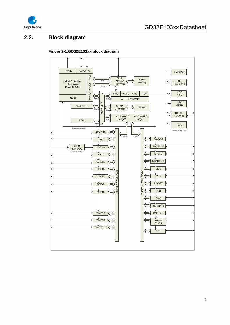
2.2. Block diagram
Figure 2-1.GD32E103xx block diagram
NVIC
TPIU
FlashMemory
Controller
FlashMemory
SRAMController
SRAM
AHB to APB Bridge 2
AHB to APB Bridge 1
USART0
SPI0
EXTI
GPIOA
GPIOB
USART1~2
SPI1~2
TIMER1~3
WWDGT
Slave
Slave
Slave
Slave Slave
Master
Ibus
Dbus
Interrput request
POR/PDR
PLLFmax : 120MHz
LDO1.2V
IRC8MHz
HXTAL4-32MHz
LVD
Powered By VDDA
Master
I2C0
I2C1
FWDGT
RTC
DAC
TIMER4~6
GPIOC
GPIOD
GPIOE
TIMER0
TIMER7
TIMER8~10
UART3~4
TIMER11~13
ADC0~1
AHB Peripherals
FMC USBFS CRC RCU
DMA 12 chs
Slave
EXMC
12-bitSAR ADC
Powered By VDDA
ARM Cortex-M4Processor
Fmax:120MHz
SW/JTAG
Sys
tem
DC
ode
ICode
AH
B M
atrix
AP
B2: F
max =
120M
Hz
AP
B1: F
max =
60M
HZ
CTC
GD32E103xx Datasheet
10
2.3. Pinouts and pin assignment
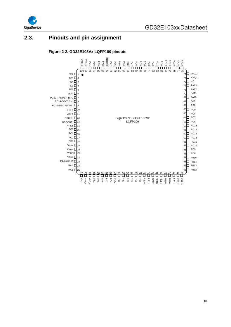
Figure 2-2. GD32E103Vx LQFP100 pinouts
13
22
23
24
26 27 28 29 30 31 32 33 34 35 36 37
100 99 98 97 96 95 94 93 92 91 90 89
OSCIN
OSCOUT
VSSA
VREF-
PA1
PC6
PD15
PD14
PD13
PD12
PD11
PD10
PD9
PD8
PB15
PB14
PB13
PA
3
VS
S_4
VD
D_4
PA
4
PA
5
PA
6
PA
7
PC
4
PC
5
PB
0
PB
1
PB
2
VD
D_3
VS
S_3
PE
1
PE
0
PB
9
PB
8
BO
OT
0
PB
7
PB
6
PB
5
PB
4
PB
3
GigaDevice GD32E103Vx
LQFP100
38 39 40 41 43 44 45 46 47 48 49
PE
7
PE
8
PE
9
PE
10
PE
11
PE
12
PE
13
PE
14
PE
15
PB
10
PB
11
VS
S_1
VDD_2
VSS_2
NC
PA13
PA12
PA11
PA10
PA9
PA8
PC9
PC8
PC7
42
88 87 86 85 84 83 82 81 80 79 78 77
PD
5
PD
4
PD
3
PD
2
PD
1
PD
0
PC
12
PC
11
PC
10
PA
15
1
2
3
4
5
6
7
8
9
10
11
12
VBAT
PC13-TAMPER-RTC
PC14-OSC32IN
PC15-OSC32OUT
NRST
VSS_5
VDD_5
PA0-WKUP
PE2 75
74
73
72
71
70
69
68
67
66
65
64
63
62
61
60
59
58
57
56
55
54
53
52
14
15
16
17
18
19
20
21
25PA2 PB1251
50
VD
D_1
PA
14
76
PE3
PE4
PE5
PE6
PC0
PC1
PC2
PC3
VREF+
VDDA
PD
6
PD
7
GD32E103xx Datasheet
11
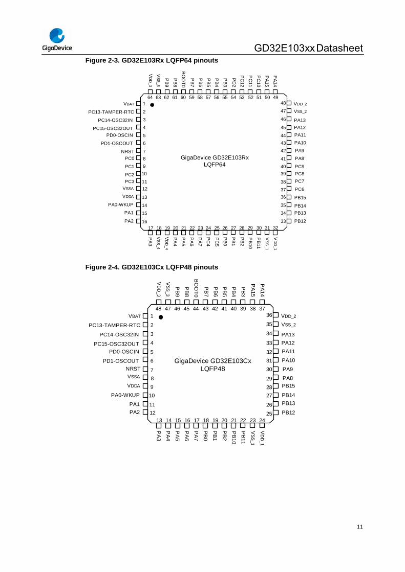
Figure 2-3. GD32E103Rx LQFP64 pinouts
4
13
14
15
17 18 19 20 21 22 23 24 25 26 27 28
64 63 62 61 60 59 58 57 56 55 54 53
VSSA
PA1
PA12
PA11
PA10
PA9
PA8
PC9
PC8
PC7
PC6
PB15
PB14
PB13
PA
3
VS
S_4
VD
D_4
PA
4
PA
5
PA
6
PA
7
PC
4
PC
5
PB
0
PB
1
PB
2
VD
D_3
VS
S_3
PB
9
PB
8
PB
7
PB
6
BO
OT
0
PB
5
PB
4
PB
3
PD
2
PC
12
GigaDevice GD32E103Rx
LQFP64
29 30 31 32
PB
10
PB
11
VS
S_1
VDD_2
VSS_2
PA13
52 51 50 49
PA
15
PA
14
1
2
3
VBAT
PC13-TAMPER-RTC
PC14-OSC32IN
PC15-OSC32OUT
NRST
PA0-WKUP
48
47
46
45
44
43
42
41
40
39
38
37
36
35
34
5
6
7
8
9
10
11
12
16PA2 PB1233
VD
D_1
PC0
PC1
PC2
PC3
VDDA
PC
10
PC
11
PD1-OSCOUT
PD0-OSCIN
Figure 2-4. GD32E103Cx LQFP48 pinouts
4
13 14 15 16 17 18 19 20 21 22 23 24
48 47 46 45 44 43 42 41 40 39 38 37
VSSA
PA1
PA12
PA11
PA10
PA9
PA8
PB15
PB14
PB13
PA
3
PA
4
PA
5
PA
6
PA
7
PB
0
PB
1
PB
2
VD
D_3
VS
S_3
PB
9
PB
8
PB
7
PB
6
BO
OT
0
PB
5
PB
4
PB
3
GigaDevice GD32E103Cx
LQFP48
PB
10
PB
11
VS
S_1
VDD_2
VSS_2
PA13
PA
15
PA
14
1
2
3
VBAT
PC13-TAMPER-RTC
PC14-OSC32IN
PC15-OSC32OUT
NRST
PA0-WKUP
36
35
34
33
32
31
30
29
28
27
26
25
5
6
7
8
9
10
11
12PA2 PB12
VD
D_1
VDDA
PD1-OSCOUT
PD0-OSCIN
GD32E103xx Datasheet
12
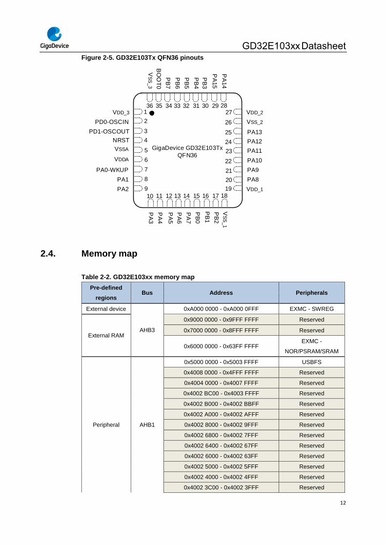
Figure 2-5. GD32E103Tx QFN36 pinouts
4
VSSA
PA1
PA12
PA11
PA10
PA9
PA8
PA
3
PA
4
PA
5
PA
6
PA
7
PB
0
PB
1
PB
2
VS
S_3
PB
7
PB
6
BO
OT
0
PB
5
PB
4
PB
3
GigaDevice GD32E103Tx
QFN36V
SS
_1
VDD_2
VSS_2
PA13
PA
15
PA
14
1
2
3
NRST
PA0-WKUP
5
6
7
8
9PA2
VDDA
10 11 12 13 14 15 16 17 18
24
27
26
25
23
22
21
20
19
36 35 34 33 32 31 30 29 28
PD1-OSCOUT
PD0-OSCIN
VDD_3
VDD_1
2.4. Memory map
Table 2-2. GD32E103xx memory map
Pre-defined
regions Bus Address Peripherals
External device
AHB3
0xA000 0000 - 0xA000 0FFF EXMC - SWREG
External RAM
0x9000 0000 - 0x9FFF FFFF Reserved
0x7000 0000 - 0x8FFF FFFF Reserved
0x6000 0000 - 0x63FF FFFF EXMC -
NOR/PSRAM/SRAM
Peripheral AHB1
0x5000 0000 - 0x5003 FFFF USBFS
0x4008 0000 - 0x4FFF FFFF Reserved
0x4004 0000 - 0x4007 FFFF Reserved
0x4002 BC00 - 0x4003 FFFF Reserved
0x4002 B000 - 0x4002 BBFF Reserved
0x4002 A000 - 0x4002 AFFF Reserved
0x4002 8000 - 0x4002 9FFF Reserved
0x4002 6800 - 0x4002 7FFF Reserved
0x4002 6400 - 0x4002 67FF Reserved
0x4002 6000 - 0x4002 63FF Reserved
0x4002 5000 - 0x4002 5FFF Reserved
0x4002 4000 - 0x4002 4FFF Reserved
0x4002 3C00 - 0x4002 3FFF Reserved
GD32E103xx Datasheet
13
Pre-defined
regions Bus Address Peripherals
0x4002 3800 - 0x4002 3BFF Reserved
0x4002 3400 - 0x4002 37FF Reserved
0x4002 3000 - 0x4002 33FF CRC
0x4002 2C00 - 0x4002 2FFF Reserved
0x4002 2800 - 0x4002 2BFF Reserved
0x4002 2400 - 0x4002 27FF Reserved
0x4002 2000 - 0x4002 23FF FMC
0x4002 1C00 - 0x4002 1FFF Reserved
0x4002 1800 - 0x4002 1BFF Reserved
0x4002 1400 - 0x4002 17FF Reserved
0x4002 1000 - 0x4002 13FF RCU
0x4002 0C00 - 0x4002 0FFF Reserved
0x4002 0800 - 0x4002 0BFF Reserved
0x4002 0400 - 0x4002 07FF DMA1
0x4002 0000 - 0x4002 03FF DMA0
0x4001 8400 - 0x4001 FFFF Reserved
0x4001 8000 - 0x4001 83FF Reserved
APB2
0x4001 7C00 - 0x4001 7FFF Reserved
0x4001 7800 - 0x4001 7BFF Reserved
0x4001 7400 - 0x4001 77FF Reserved
0x4001 7000 - 0x4001 73FF Reserved
0x4001 6C00 - 0x4001 6FFF Reserved
0x4001 6800 - 0x4001 6BFF Reserved
0x4001 5C00 - 0x4001 67FF Reserved
0x4001 5800 - 0x4001 5BFF Reserved
0x4001 5400 - 0x4001 57FF TIMER10
0x4001 5000 - 0x4001 53FF TIMER9
0x4001 4C00 - 0x4001 4FFF TIMER8
0x4001 4800 - 0x4001 4BFF Reserved
0x4001 4400 - 0x4001 47FF Reserved
0x4001 4000 - 0x4001 43FF Reserved
0x4001 3C00 - 0x4001 3FFF Reserved
0x4001 3800 - 0x4001 3BFF USART0
0x4001 3400 - 0x4001 37FF TIMER7
0x4001 3000 - 0x4001 33FF SPI0
0x4001 2C00 - 0x4001 2FFF TIMER0
0x4001 2800 - 0x4001 2BFF ADC1
0x4001 2400 - 0x4001 27FF ADC0
0x4001 2000 - 0x4001 23FF Reserved
GD32E103xx Datasheet
14
Pre-defined
regions Bus Address Peripherals
0x4001 1C00 - 0x4001 1FFF Reserved
0x4001 1800 - 0x4001 1BFF GPIOE
0x4001 1400 - 0x4001 17FF GPIOD
0x4001 1000 - 0x4001 13FF GPIOC
0x4001 0C00 - 0x4001 0FFF GPIOB
0x4001 0800 - 0x4001 0BFF GPIOA
0x4001 0400 - 0x4001 07FF EXTI
0x4001 0000 - 0x4001 03FF AFIO
APB1
0x4000 CC00 - 0x4000 FFFF Reserved
0x4000 C800 - 0x4000 CBFF CTC
0x4000 C400 - 0x4000 C7FF Reserved
0x4000 C000 - 0x4000 C3FF Reserved
0x4000 8000 - 0x4000 BFFF Reserved
0x4000 7C00 - 0x4000 7FFF Reserved
0x4000 7800 - 0x4000 7BFF Reserved
0x4000 7400 - 0x4000 77FF DAC
0x4000 7000 - 0x4000 73FF PMU
0x4000 6C00 - 0x4000 6FFF BKP
0x4000 6800 - 0x4000 6BFF Reserved
0x4000 6400 - 0x4000 67FF Reserved
0x4000 6000 - 0x4000 63FF Reserved
0x4000 5C00 - 0x4000 5FFF Reserved
0x4000 5800 - 0x4000 5BFF I2C1
0x4000 5400 - 0x4000 57FF I2C0
0x4000 5000 - 0x4000 53FF UART4
0x4000 4C00 - 0x4000 4FFF UART3
0x4000 4800 - 0x4000 4BFF USART2
0x4000 4400 - 0x4000 47FF USART1
0x4000 4000 - 0x4000 43FF Reserved
0x4000 3C00 - 0x4000 3FFF SPI2/I2S2
0x4000 3800 - 0x4000 3BFF SPI1/I2S1
0x4000 3400 - 0x4000 37FF Reserved
0x4000 3000 - 0x4000 33FF FWDGT
0x4000 2C00 - 0x4000 2FFF WWDGT
0x4000 2800 - 0x4000 2BFF RTC
0x4000 2400 - 0x4000 27FF Reserved
0x4000 2000 - 0x4000 23FF TIMER13
0x4000 1C00 - 0x4000 1FFF TIMER12
0x4000 1800 - 0x4000 1BFF TIMER11
GD32E103xx Datasheet
15
Pre-defined
regions Bus Address Peripherals
0x4000 1400 - 0x4000 17FF TIMER6
0x4000 1000 - 0x4000 13FF TIMER5
0x4000 0C00 - 0x4000 0FFF TIMER4
0x4000 0800 - 0x4000 0BFF TIMER3
0x4000 0400 - 0x4000 07FF TIMER2
0x4000 0000 - 0x4000 03FF TIMER1
SRAM AHB
0x2007 0000 - 0x3FFF FFFF Reserved
0x2006 0000 - 0x2006 FFFF Reserved
0x2003 0000 - 0x2005 FFFF Reserved
0x2002 0000 - 0x2002 FFFF Reserved
0x2001 C000 - 0x2001 FFFF
SRAM 0x2001 8000 - 0x2001 BFFF
0x2000 5000 - 0x2001 7FFF
0x2000 0000 - 0x2000 4FFF
Code AHB
0x1FFF F810 - 0x1FFF FFFF Reserved
0x1FFF F800 - 0x1FFF F80F Option Bytes
0x1FFF F000 - 0x1FFF F7FF
Boot loader 0x1FFF C010 - 0x1FFF EFFF
0x1FFF C000 - 0x1FFF C00F
0x1FFF B000 - 0x1FFF BFFF
0x1FFF 7A10 - 0x1FFF AFFF Reserved
0x1FFF 7800 - 0x1FFF 7A0F Reserved
0x1FFF 0000 - 0x1FFF 77FF Reserved
0x1FFE C010 - 0x1FFE FFFF Reserved
0x1FFE C000 - 0x1FFE C00F Reserved
0x1001 0000 - 0x1FFE BFFF Reserved
0x1000 0000 - 0x1000 FFFF Reserved
0x083C 0000 - 0x0FFF FFFF Reserved
0x0830 0000 - 0x083B FFFF Reserved
0x0810 0000 - 0x082F FFFF
Main Flash 0x0802 0000 - 0x080F FFFF
0x0800 0000 - 0x0801 FFFF
0x0030 0000 - 0x07FF FFFF Reserved
0x0010 0000 - 0x002F FFFF Aliased to Main Flash or
Boot loader 0x0002 0000 - 0x000F FFFF
0x0000 0000 - 0x0001 FFFF
GD32E103xx Datasheet
16
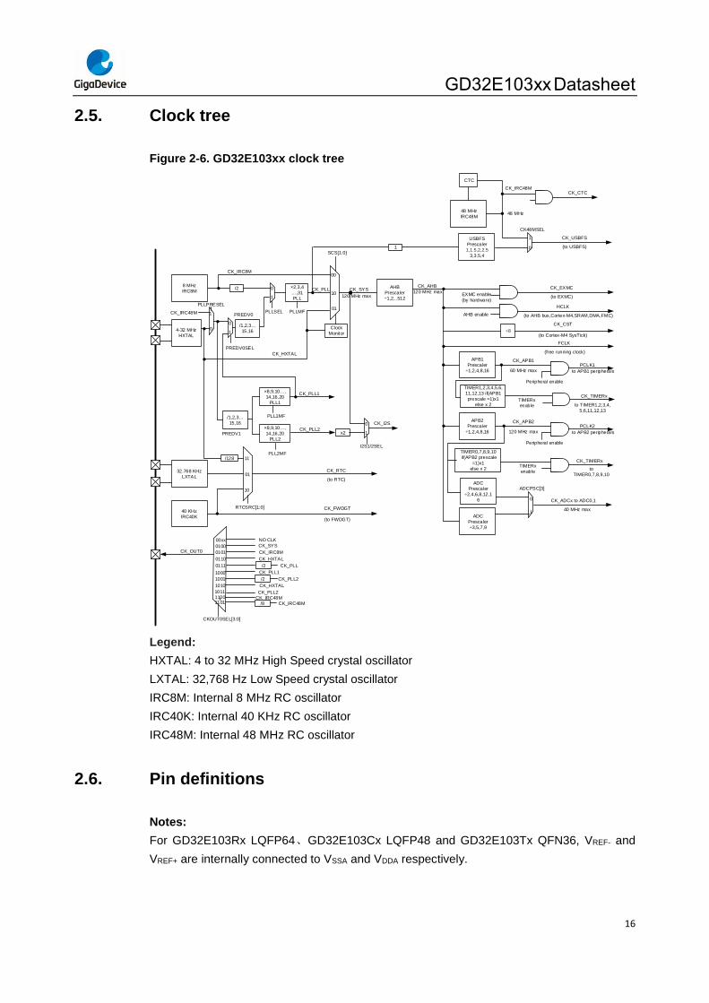
2.5. Clock tree
Figure 2-6. GD32E103xx clock tree
/2
4-32 MHz
HXTAL
8 MHz
IRC8M×2,3,4
…,31
PLL
Clock
Monitor
PLLSEL PLLMF
0
1
00
01
10
CK_IRC8M
CK_HXTAL
CK_PLL CK_SYS
120 MHz max
AHB
Prescaler
÷1,2...512
CK_AHB
120 MHz max
APB1
Prescaler
÷1,2,4,8,16
TIMER1,2,3,4,5,6,
11,12,13 if(APB1
prescale =1)x1
else x 2
APB2
Prescaler
÷1,2,4,8,16
TIMER0,7,8,9,10
if(APB2 prescale
=1)x1
else x 2
ADC
Prescaler
÷2,4,6,8,12,1
6
CK_APB2
120 MHz max
Peripheral enable
PCLK2
to APB2 peripherals
CK_APB1
60 MHz max
Peripheral enable
PCLK1
to APB1 peripherals
TIMERx
enable
CK_TIMERx
to
TIMER0,7,8,9,10
TIMERx
enable
CK_TIMERx
to TIMER1,2,3,4,
5,6,11,12,13
CK_ADCx to ADC0,1
40 MHz max
AHB enable
HCLK
(to AHB bus,Cortex-M4,SRAM,DMA,FMC)
EXMC enable
(by hardware)
CK_EXMC
(to EXMC)
÷8
CK_CST
(to Cortex-M4 SysTick)
FCLK
(free running clock)
USBFS
Prescaler
1,1.5,2,2.5
3,3.5,4
CK_USBFS
(to USBFS)
32.768 KHz
LXTAL
11
10
01
40 KHz
IRC40K
CK_RTC
CK_FWDGT
(to RTC)
(to FWDGT)
/128
CK_OUT0
SCS[1:0]
RTCSRC[1:0]
PREDV0
0
1
CK_PLL
CK_HXTAL
CK_IRC8M
CK_SYS
/20111
00xx NO CLK 0100
0101
0110
CKOUT0SEL[3:0]
48 MHz
/2
1000
1001
1010
CK_PLL1
CK_PLL2
1011 CK_PLL2
/1,2,3…
15,16
PREDV1
×8,9,10…,
14,16,20
PLL1
PLL1MF
PLL2MF
×8,9,10…,
14,16,20
PLL2
CK_PLL1
CK_PLL2
/1,2,3…
15,16
x2
I2S1/2SEL
0
1
CK_I2S
1
PREDV0SEL
48 MHz
IRC48M
CTC
CK48MSEL
CK_CTC
1
0
1
0
CK_IRC48M
PLLPRESEL
ADC
Prescaler
÷3,5,7,9
0
1
ADCPSC[3]
CK_IRC48M
CK_HXTAL
11001101
CK_IRC48M
/8 CK_IRC48M
Legend:
HXTAL: 4 to 32 MHz High Speed crystal oscillator
LXTAL: 32,768 Hz Low Speed crystal oscillator
IRC8M: Internal 8 MHz RC oscillator
IRC40K: Internal 40 KHz RC oscillator
IRC48M: Internal 48 MHz RC oscillator
2.6. Pin definitions
Notes:
For GD32E103Rx LQFP64、GD32E103Cx LQFP48 and GD32E103Tx QFN36, VREF- and
VREF+ are internally connected to VSSA and VDDA respectively.
GD32E103xx Datasheet
17
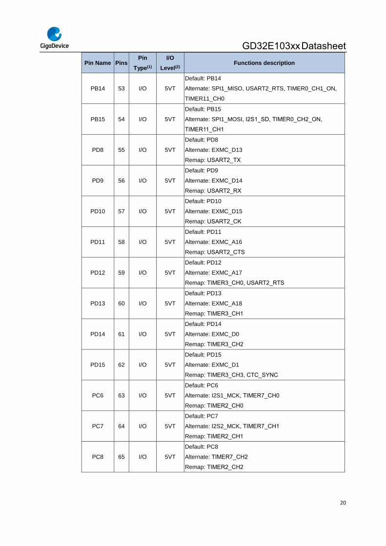
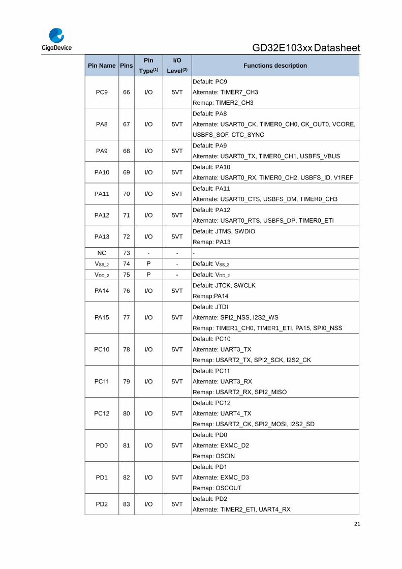
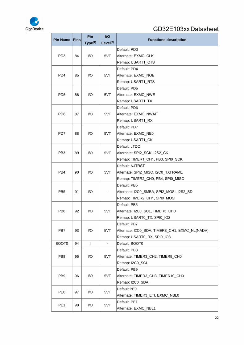
2.6.1. GD32E103Vx LQFP100 pin definitions
Table 2-3. GD32E103Vx LQFP100 pin definitions
Pin Name Pins Pin
Type(1)
I/O
Level(2) Functions description
PE2 1 I/O 5VT Default: PE2
Alternate: EXMC_A23
PE3 2 I/O 5VT Default: PE3
Alternate: EXMC_A19
PE4 3 I/O 5VT Default: PE4
Alternate: EXMC_A20
PE5 4 I/O 5VT
Default: PE5
Alternate: EXMC_A21
Remap: TIMER8_CH0
PE6 5 I/O 5VT
Default: PE6
Alternate: EXMC_A22
Remap: TIMER8_CH1
VBAT 6 P - Default: VBAT
PC13-
TAMPER-
RTC
7 I/O - Default: PC13
Alternate: RTC_TAMPER
PC14-
OSC32IN 8 I/O -
Default: PC14
Alternate: OSC32IN
PC15-
OSC32OU
T
9 I/O - Default: PC15
Alternate: OSC32OUT
VSS_5 10 P - Default: VSS_5
VDD_5 11 P - Default: VDD_5
OSCIN 12 I - Default: OSCIN
Remap: PD0
OSCOUT 13 O - Default: OSCOUT
Remap:PD1
NRST 14 I/O - Default: NRST
PC0 15 I/O - Default: PC0
Alternate: ADC01_IN10
PC1 16 I/O - Default: PC1
Alternate: ADC01_IN11
PC2 17 I/O - Default: PC2
Alternate: ADC01_IN12
PC3 18 I/O - Default: PC3
Alternate: ADC01_IN13
VSSA 19 P - Default: VSSA
VREF- 20 P - Default: VREF-
GD32E103xx Datasheet
18
Pin Name Pins Pin
Type(1)
I/O
Level(2) Functions description
VREF+ 21 P - Default: VREF+
VDDA 22 P - Default: VDDA
PA0-WKUP 23 I/O -
Default: PA0
Alternate: WKUP, USART1_CTS, ADC01_IN0,
TIMER1_CH0, TIMER1_ETI, TIMER4_CH0, TIMER7_ETI
PA1 24 I/O -
Default: PA1
Alternate: USART1_RTS, ADC01_IN1, TIMER4_CH1,
TIMER1_CH1
PA2 25 I/O -
Default: PA2
Alternate: USART1_TX, TIMER4_CH2, ADC01_IN2,
TIMER8_CH0, TIMER1_CH2, SPI0_IO2
PA3 26 I/O -
Default: PA3
Alternate: USART1_RX, TIMER4_CH3, ADC01_IN3,
TIMER1_CH3, TIMER8_CH1, SPI0_IO3
VSS_4 27 P - Default: VSS_4
VDD_4 28 P - Default: VDD_4
PA4 29 I/O -
Default: PA4
Alternate: SPI0_NSS, USART1_CK, DAC_OUT0,
ADC01_IN4
Remap: SPI2_NSS, I2S2_WS
PA5 30 I/O - Default: PA5
Alternate: SPI0_SCK, ADC01_IN5, DAC_OUT1
PA6 31 I/O -
Default: PA6
Alternate: SPI0_MISO, TIMER7_BRKIN, ADC01_IN6,
TIMER2_CH0, TIMER12_CH0
Remap: TIMER0_BRKIN
PA7 32 I/O -
Default: PA7
Alternate: SPI0_MOSI, TIMER7_CH0_ON, ADC01_IN7,
TIMER2_CH1, TIMER13_CH0
Remap: TIMER0_CH0_ON
PC4 33 I/O - Default: PC4
Alternate: ADC01_IN14
PC5 34 I/O - Default: PC5
Alternate: ADC01_IN15
PB0 35 I/O -
Default: PB0
Alternate: ADC01_IN8, TIMER2_CH2, TIMER7_CH1_ON
Remap: TIMER0_CH1_ON
PB1 36 I/O -
Default: PB1
Alternate: ADC01_IN9, TIMER2_CH3, TIMER7_CH2_ON
Remap: TIMER0_CH2_ON
PB2 37 I/O 5VT Default: PB2, BOOT1
GD32E103xx Datasheet
19
Pin Name Pins Pin
Type(1)
I/O
Level(2) Functions description
PE7 38 I/O 5VT
Default: PE7
Alternate: EXMC_D4
Remap: TIMER0_ETI
PE8 39 I/O 5VT
Default: PE8
Alternate: EXMC_D5
Remap: TIMER0_CH0_ON
PE9 40 I/O 5VT
Default: PE9
Alternate: EXMC_D6
Remap: TIMER0_CH0
PE10 41 I/O 5VT
Default: PE10
Alternate: EXMC_D7
Remap: TIMER0_CH1_ON
PE11 42 I/O 5VT
Default: PE11
Alternate: EXMC_D8
Remap: TIMER0_CH1
PE12 43 I/O 5VT
Default: PE12
Alternate: EXMC_D9
Remap: TIMER0_CH2_ON
PE13 44 I/O 5VT
Default: PE13
Alternate: EXMC_D10
Remap: TIMER0_CH2
PE14 45 I/O 5VT
Default: PE14
Alternate: EXMC_D11
Remap: TIMER0_CH3
PE15 46 I/O 5VT
Default: PE15
Alternate: EXMC_D12
Remap: TIMER0_BRKIN
PB10 47 I/O 5VT
Default: PB10
Alternate: I2C1_SCL, USART2_TX
Remap: TIMER1_CH2
PB11 48 I/O 5VT
Default: PB11
Alternate: I2C1_SDA, USART2_RX
Remap: TIMER1_CH3
VSS_1 49 P - Default: VSS_1
VDD_1 50 P - Default: VDD_1
PB12 51 I/O 5VT
Default: PB12
Alternate: SPI1_NSS, I2S1_WS, I2C1_SMBA, USART2_CK,
TIMER0_BRKIN
PB13 52 I/O 5VT
Default: PB13
Alternate: SPI1_SCK, I2S1_CK, USART2_CTS,
TIMER0_CH0_ON, I2C1_TXFRAME
GD32E103xx Datasheet
20
Pin Name Pins Pin
Type(1)
I/O
Level(2) Functions description
PB14 53 I/O 5VT
Default: PB14
Alternate: SPI1_MISO, USART2_RTS, TIMER0_CH1_ON,
TIMER11_CH0
PB15 54 I/O 5VT
Default: PB15
Alternate: SPI1_MOSI, I2S1_SD, TIMER0_CH2_ON,
TIMER11_CH1
PD8 55 I/O 5VT
Default: PD8
Alternate: EXMC_D13
Remap: USART2_TX
PD9 56 I/O 5VT
Default: PD9
Alternate: EXMC_D14
Remap: USART2_RX
PD10 57 I/O 5VT
Default: PD10
Alternate: EXMC_D15
Remap: USART2_CK
PD11 58 I/O 5VT
Default: PD11
Alternate: EXMC_A16
Remap: USART2_CTS
PD12 59 I/O 5VT
Default: PD12
Alternate: EXMC_A17
Remap: TIMER3_CH0, USART2_RTS
PD13 60 I/O 5VT
Default: PD13
Alternate: EXMC_A18
Remap: TIMER3_CH1
PD14 61 I/O 5VT
Default: PD14
Alternate: EXMC_D0
Remap: TIMER3_CH2
PD15 62 I/O 5VT
Default: PD15
Alternate: EXMC_D1
Remap: TIMER3_CH3, CTC_SYNC
PC6 63 I/O 5VT
Default: PC6
Alternate: I2S1_MCK, TIMER7_CH0
Remap: TIMER2_CH0
PC7 64 I/O 5VT
Default: PC7
Alternate: I2S2_MCK, TIMER7_CH1
Remap: TIMER2_CH1
PC8 65 I/O 5VT
Default: PC8
Alternate: TIMER7_CH2
Remap: TIMER2_CH2
GD32E103xx Datasheet
21
Pin Name Pins Pin
Type(1)
I/O
Level(2) Functions description
PC9 66 I/O 5VT
Default: PC9
Alternate: TIMER7_CH3
Remap: TIMER2_CH3
PA8 67 I/O 5VT
Default: PA8
Alternate: USART0_CK, TIMER0_CH0, CK_OUT0, VCORE,
USBFS_SOF, CTC_SYNC
PA9 68 I/O 5VT Default: PA9
Alternate: USART0_TX, TIMER0_CH1, USBFS_VBUS
PA10 69 I/O 5VT Default: PA10
Alternate: USART0_RX, TIMER0_CH2, USBFS_ID, V1REF
PA11 70 I/O 5VT Default: PA11
Alternate: USART0_CTS, USBFS_DM, TIMER0_CH3
PA12 71 I/O 5VT Default: PA12
Alternate: USART0_RTS, USBFS_DP, TIMER0_ETI
PA13 72 I/O 5VT Default: JTMS, SWDIO
Remap: PA13
NC 73 - - -
VSS_2 74 P - Default: VSS_2
VDD_2 75 P - Default: VDD_2
PA14 76 I/O 5VT Default: JTCK, SWCLK
Remap:PA14
PA15 77 I/O 5VT
Default: JTDI
Alternate: SPI2_NSS, I2S2_WS
Remap: TIMER1_CH0, TIMER1_ETI, PA15, SPI0_NSS
PC10 78 I/O 5VT
Default: PC10
Alternate: UART3_TX
Remap: USART2_TX, SPI2_SCK, I2S2_CK
PC11 79 I/O 5VT
Default: PC11
Alternate: UART3_RX
Remap: USART2_RX, SPI2_MISO
PC12 80 I/O 5VT
Default: PC12
Alternate: UART4_TX
Remap: USART2_CK, SPI2_MOSI, I2S2_SD
PD0 81 I/O 5VT
Default: PD0
Alternate: EXMC_D2
Remap: OSCIN
PD1 82 I/O 5VT
Default: PD1
Alternate: EXMC_D3
Remap: OSCOUT
PD2 83 I/O 5VT Default: PD2
Alternate: TIMER2_ETI, UART4_RX
GD32E103xx Datasheet
22
Pin Name Pins Pin
Type(1)
I/O
Level(2) Functions description
PD3 84 I/O 5VT
Default: PD3
Alternate: EXMC_CLK
Remap: USART1_CTS
PD4 85 I/O 5VT
Default: PD4
Alternate: EXMC_NOE
Remap: USART1_RTS
PD5 86 I/O 5VT
Default: PD5
Alternate: EXMC_NWE
Remap: USART1_TX
PD6 87 I/O 5VT
Default: PD6
Alternate: EXMC_NWAIT
Remap: USART1_RX
PD7 88 I/O 5VT
Default: PD7
Alternate: EXMC_NE0
Remap: USART1_CK
PB3 89 I/O 5VT
Default: JTDO
Alternate: SPI2_SCK, I2S2_CK
Remap: TIMER1_CH1, PB3, SPI0_SCK
PB4 90 I/O 5VT
Default: NJTRST
Alternate: SPI2_MISO, I2C0_TXFRAME
Remap: TIMER2_CH0, PB4, SPI0_MISO
PB5 91 I/O -
Default: PB5
Alternate: I2C0_SMBA, SPI2_MOSI, I2S2_SD
Remap: TIMER2_CH1, SPI0_MOSI
PB6 92 I/O 5VT
Default: PB6
Alternate: I2C0_SCL, TIMER3_CH0
Remap: USART0_TX, SPI0_IO2
PB7 93 I/O 5VT
Default: PB7
Alternate: I2C0_SDA, TIMER3_CH1, EXMC_NL(NADV)
Remap: USART0_RX, SPI0_IO3
BOOT0 94 I - Default: BOOT0
PB8 95 I/O 5VT
Default: PB8
Alternate: TIMER3_CH2, TIMER9_CH0
Remap: I2C0_SCL
PB9 96 I/O 5VT
Default: PB9
Alternate: TIMER3_CH3, TIMER10_CH0
Remap: I2C0_SDA
PE0 97 I/O 5VT Default:PE0
Alternate: TIMER3_ETI, EXMC_NBL0
PE1 98 I/O 5VT Default: PE1
Alternate: EXMC_NBL1
GD32E103xx Datasheet
23
Pin Name Pins Pin
Type(1)
I/O
Level(2) Functions description
VSS_3 99 P - Default: VSS_3
VDD_3 100 P - Default: VDD_3
Notes:
1. Type: I= input, O = output, P = power.
2. I/O Level: 5VT = 5V tolerant.
3. Functions are available in GD32E103xx devices.
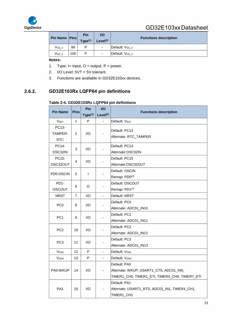
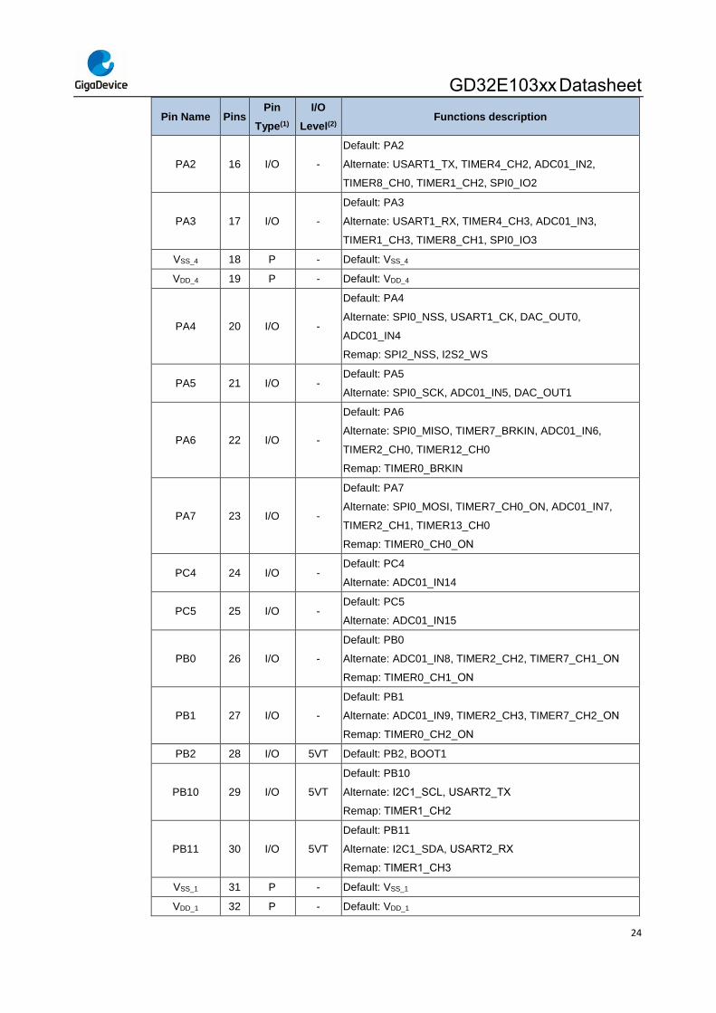
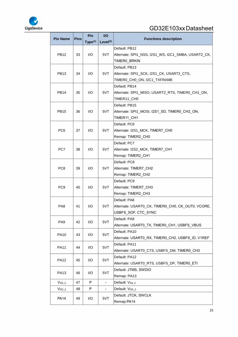
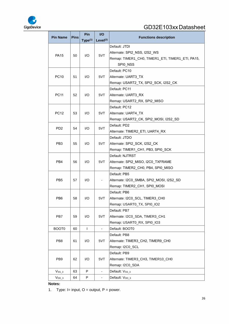
2.6.2. GD32E103Rx LQFP64 pin definitions
Table 2-4. GD32E103Rx LQFP64 pin definitions
Pin Name Pins Pin
Type(1)
I/O
Level(2) Functions description
VBAT 1 P - Default: VBAT
PC13-
TAMPER-
RTC
2 I/O - Default: PC13
Alternate: RTC_TAMPER
PC14-
OSC32IN 3 I/O -
Default: PC14
Alternate:OSC32IN
PC15-
OSC32OUT 4 I/O -
Default: PC15
Alternate:OSC32OUT
PD0-OSCIN 5 I - Default: OSCIN
Remap: PD0(3)
PD1-
OSCOUT 6 O -
Default: OSCOUT
Remap: PD1(3)
NRST 7 I/O - Default: NRST
PC0 8 I/O - Default: PC0
Alternate: ADC01_IN10
PC1 9 I/O - Default: PC1
Alternate: ADC01_IN11
PC2 10 I/O - Default: PC2
Alternate: ADC01_IN12
PC3 11 I/O - Default: PC3
Alternate: ADC01_IN13
VSSA 12 P - Default: VSSA
VDDA 13 P - Default: VDDA
PA0-WKUP 14 I/O -
Default: PA0
Alternate: WKUP, USART1_CTS, ADC01_IN0,
TIMER1_CH0, TIMER1_ETI, TIMER4_CH0, TIMER7_ETI
PA1 15 I/O -
Default: PA1
Alternate: USART1_RTS, ADC01_IN1, TIMER4_CH1,
TIMER1_CH1
GD32E103xx Datasheet
24
Pin Name Pins Pin
Type(1)
I/O
Level(2) Functions description
PA2 16 I/O -
Default: PA2
Alternate: USART1_TX, TIMER4_CH2, ADC01_IN2,
TIMER8_CH0, TIMER1_CH2, SPI0_IO2
PA3 17 I/O -
Default: PA3
Alternate: USART1_RX, TIMER4_CH3, ADC01_IN3,
TIMER1_CH3, TIMER8_CH1, SPI0_IO3
VSS_4 18 P - Default: VSS_4
VDD_4 19 P - Default: VDD_4
PA4 20 I/O -
Default: PA4
Alternate: SPI0_NSS, USART1_CK, DAC_OUT0,
ADC01_IN4
Remap: SPI2_NSS, I2S2_WS
PA5 21 I/O - Default: PA5
Alternate: SPI0_SCK, ADC01_IN5, DAC_OUT1
PA6 22 I/O -
Default: PA6
Alternate: SPI0_MISO, TIMER7_BRKIN, ADC01_IN6,
TIMER2_CH0, TIMER12_CH0
Remap: TIMER0_BRKIN
PA7 23 I/O -
Default: PA7
Alternate: SPI0_MOSI, TIMER7_CH0_ON, ADC01_IN7,
TIMER2_CH1, TIMER13_CH0
Remap: TIMER0_CH0_ON
PC4 24 I/O - Default: PC4
Alternate: ADC01_IN14
PC5 25 I/O - Default: PC5
Alternate: ADC01_IN15
PB0 26 I/O -
Default: PB0
Alternate: ADC01_IN8, TIMER2_CH2, TIMER7_CH1_ON
Remap: TIMER0_CH1_ON
PB1 27 I/O -
Default: PB1
Alternate: ADC01_IN9, TIMER2_CH3, TIMER7_CH2_ON
Remap: TIMER0_CH2_ON
PB2 28 I/O 5VT Default: PB2, BOOT1
PB10 29 I/O 5VT
Default: PB10
Alternate: I2C1_SCL, USART2_TX
Remap: TIMER1_CH2
PB11 30 I/O 5VT
Default: PB11
Alternate: I2C1_SDA, USART2_RX
Remap: TIMER1_CH3
VSS_1 31 P - Default: VSS_1
VDD_1 32 P - Default: VDD_1
GD32E103xx Datasheet
25
Pin Name Pins Pin
Type(1)
I/O
Level(2) Functions description
PB12 33 I/O 5VT
Default: PB12
Alternate: SPI1_NSS, I2S1_WS, I2C1_SMBA, USART2_CK,
TIMER0_BRKIN
PB13 34 I/O 5VT
Default: PB13
Alternate: SPI1_SCK, I2S1_CK, USART2_CTS,
TIMER0_CH0_ON, I2C1_TXFRAME
PB14 35 I/O 5VT
Default: PB14
Alternate: SPI1_MISO, USART2_RTS, TIMER0_CH1_ON,
TIMER11_CH0
PB15 36 I/O 5VT
Default: PB15
Alternate: SPI1_MOSI, I2S1_SD, TIMER0_CH2_ON,
TIMER11_CH1
PC6 37 I/O 5VT
Default: PC6
Alternate: I2S1_MCK, TIMER7_CH0
Remap: TIMER2_CH0
PC7 38 I/O 5VT
Default: PC7
Alternate: I2S2_MCK, TIMER7_CH1
Remap: TIMER2_CH1
PC8 39 I/O 5VT
Default: PC8
Alternate: TIMER7_CH2
Remap: TIMER2_CH2
PC9 40 I/O 5VT
Default: PC9
Alternate: TIMER7_CH3
Remap: TIMER2_CH3
PA8 41 I/O 5VT
Default: PA8
Alternate: USART0_CK, TIMER0_CH0, CK_OUT0, VCORE,
USBFS_SOF, CTC_SYNC
PA9 42 I/O 5VT Default: PA9
Alternate: USART0_TX, TIMER0_CH1, USBFS_VBUS
PA10 43 I/O 5VT Default: PA10
Alternate: USART0_RX, TIMER0_CH2, USBFS_ID, V1REF
PA11 44 I/O 5VT Default: PA11
Alternate: USART0_CTS, USBFS_DM, TIMER0_CH3
PA12 45 I/O 5VT Default: PA12
Alternate: USART0_RTS, USBFS_DP, TIMER0_ETI
PA13 46 I/O 5VT Default: JTMS, SWDIO
Remap: PA13
VSS_2 47 P - Default: VSS_2
VDD_2 48 P - Default: VDD_2
PA14 49 I/O 5VT Default: JTCK, SWCLK
Remap:PA14
GD32E103xx Datasheet
26
Pin Name Pins Pin
Type(1)
I/O
Level(2) Functions description
PA15 50 I/O 5VT
Default: JTDI
Alternate: SPI2_NSS, I2S2_WS
Remap: TIMER1_CH0, TIMER1_ETI, TIMER1_ETI, PA15,
SPI0_NSS
PC10 51 I/O 5VT
Default: PC10
Alternate: UART3_TX
Remap: USART2_TX, SPI2_SCK, I2S2_CK
PC11 52 I/O 5VT
Default: PC11
Alternate: UART3_RX
Remap: USART2_RX, SPI2_MISO
PC12 53 I/O 5VT
Default: PC12
Alternate: UART4_TX
Remap: USART2_CK, SPI2_MOSI, I2S2_SD
PD2 54 I/O 5VT Default: PD2
Alternate: TIMER2_ETI, UART4_RX
PB3 55 I/O 5VT
Default: JTDO
Alternate: SPI2_SCK, I2S2_CK
Remap: TIMER1_CH1, PB3, SPI0_SCK
PB4 56 I/O 5VT
Default: NJTRST
Alternate: SPI2_MISO, I2C0_TXFRAME
Remap: TIMER2_CH0, PB4, SPI0_MISO
PB5 57 I/O -
Default: PB5
Alternate: I2C0_SMBA, SPI2_MOSI, I2S2_SD
Remap: TIMER2_CH1, SPI0_MOSI
PB6 58 I/O 5VT
Default: PB6
Alternate: I2C0_SCL, TIMER3_CH0
Remap: USART0_TX, SPI0_IO2
PB7 59 I/O 5VT
Default: PB7
Alternate: I2C0_SDA, TIMER3_CH1
Remap: USART0_RX, SPI0_IO3
BOOT0 60 I - Default: BOOT0
PB8 61 I/O 5VT
Default: PB8
Alternate: TIMER3_CH2, TIMER9_CH0
Remap: I2C0_SCL
PB9 62 I/O 5VT
Default: PB9
Alternate: TIMER3_CH3, TIMER10_CH0
Remap: I2C0_SDA
VSS_3 63 P - Default: VSS_3
VDD_3 64 P - Default: VDD_3
Notes:
1. Type: I= input, O = output, P = power.
GD32E103xx Datasheet
27
2. I/O Level: 5VT = 5V tolerant.
3. PD0/PD1 cannot be used for EXTI in this package.
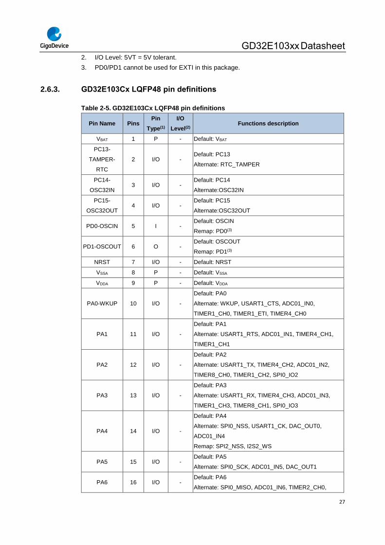
2.6.3. GD32E103Cx LQFP48 pin definitions
Table 2-5. GD32E103Cx LQFP48 pin definitions
Pin Name Pins Pin
Type(1)
I/O
Level(2) Functions description
VBAT 1 P - Default: VBAT
PC13-
TAMPER-
RTC
2 I/O - Default: PC13
Alternate: RTC_TAMPER
PC14-
OSC32IN 3 I/O -
Default: PC14
Alternate:OSC32IN
PC15-
OSC32OUT 4 I/O -
Default: PC15
Alternate:OSC32OUT
PD0-OSCIN 5 I - Default: OSCIN
Remap: PD0(3)
PD1-OSCOUT 6 O - Default: OSCOUT
Remap: PD1(3)
NRST 7 I/O - Default: NRST
VSSA 8 P - Default: VSSA
VDDA 9 P - Default: VDDA
PA0-WKUP 10 I/O -
Default: PA0
Alternate: WKUP, USART1_CTS, ADC01_IN0,
TIMER1_CH0, TIMER1_ETI, TIMER4_CH0
PA1 11 I/O -
Default: PA1
Alternate: USART1_RTS, ADC01_IN1, TIMER4_CH1,
TIMER1_CH1
PA2 12 I/O -
Default: PA2
Alternate: USART1_TX, TIMER4_CH2, ADC01_IN2,
TIMER8_CH0, TIMER1_CH2, SPI0_IO2
PA3 13 I/O -
Default: PA3
Alternate: USART1_RX, TIMER4_CH3, ADC01_IN3,
TIMER1_CH3, TIMER8_CH1, SPI0_IO3
PA4 14 I/O -
Default: PA4
Alternate: SPI0_NSS, USART1_CK, DAC_OUT0,
ADC01_IN4
Remap: SPI2_NSS, I2S2_WS
PA5 15 I/O - Default: PA5
Alternate: SPI0_SCK, ADC01_IN5, DAC_OUT1
PA6 16 I/O - Default: PA6
Alternate: SPI0_MISO, ADC01_IN6, TIMER2_CH0,
GD32E103xx Datasheet
28
Pin Name Pins Pin
Type(1)
I/O
Level(2) Functions description
TIMER12_CH0
Remap: TIMER0_BRKIN
PA7 17 I/O -
Default: PA7
Alternate: SPI0_MOSI, ADC01_IN7, TIMER2_CH1,
TIMER13_CH0
Remap: TIMER0_CH0_ON
PB0 18 I/O -
Default: PB0
Alternate: ADC01_IN8, TIMER2_CH2
Remap: TIMER0_CH1_ON
PB1 19 I/O -
Default: PB1
Alternate: ADC01_IN9, TIMER2_CH3
Remap: TIMER0_CH2_ON
PB2 20 I/O 5VT Default: PB2, BOOT1
PB10 21 I/O 5VT
Default: PB10
Alternate: I2C1_SCL, USART2_TX
Remap: TIMER1_CH2
PB11 22 I/O 5VT
Default: PB11
Alternate: I2C1_SDA, USART2_RX
Remap: TIMER1_CH3
VSS_1 23 P - Default: VSS_1
VDD_1 24 P - Default: VDD_1
PB12 25 I/O 5VT
Default: PB12
Alternate: SPI1_NSS, I2S1_WS, I2C1_SMBA,
USART2_CK, TIMER0_BRKIN
PB13 26 I/O 5VT
Default: PB13
Alternate: SPI1_SCK, I2S1_CK, USART2_CTS,
TIMER0_CH0_ON, I2C1_TXFRAME
PB14 27 I/O 5VT
Default: PB14
Alternate: SPI1_MISO, USART2_RTS,
TIMER0_CH1_ON, TIMER11_CH0
PB15 28 I/O 5VT
Default: PB15
Alternate: SPI1_MOSI, I2S1_SD, TIMER0_CH2_ON,
TIMER11_CH1
PA8 29 I/O 5VT
Default: PA8
Alternate: USART0_CK, TIMER0_CH0, CK_OUT0,
VCORE, USBFS_SOF, CTC_SYNC
PA9 30 I/O 5VT Default: PA9
Alternate: USART0_TX, TIMER0_CH1, USBFS_VBUS
PA10 31 I/O 5VT
Default: PA10
Alternate: USART0_RX, TIMER0_CH2, USBFS_ID,
V1REF
GD32E103xx Datasheet
29
Pin Name Pins Pin
Type(1)
I/O
Level(2) Functions description
PA11 32 I/O 5VT Default: PA11
Alternate: USART0_CTS, USBFS_DM, TIMER0_CH3
PA12 33 I/O 5VT Default: PA12
Alternate: USART0_RTS, USBFS_DP, TIMER0_ETI
PA13 34 I/O 5VT Default: JTMS, SWDIO
Remap: PA13
VSS_2 35 P - Default: VSS_2
VDD_2 36 P - Default: VDD_2
PA14 37 I/O 5VT Default: JTCK, SWCLK
Remap:PA14
PA15 38 I/O 5VT
Default: JTDI
Alternate: SPI2_NSS, I2S2_WS
Remap: TIMER1_CH0, TIMER1_ETI, TIMER1_ETI,
PA15, SPI0_NSS
PB3 39 I/O 5VT
Default: JTDO
Alternate: SPI2_SCK, I2S2_CK
Remap: TIMER1_CH1, PB3, SPI0_SCK
PB4 40 I/O 5VT
Default: NJTRST
Alternate: SPI2_MISO, I2C0_TXFRAME
Remap: TIMER2_CH0, PB4, SPI0_MISO
PB5 41 I/O -
Default: PB5
Alternate: I2C0_SMBA, SPI2_MOSI, I2S2_SD
Remap: TIMER2_CH1, SPI0_MOSI
PB6 42 I/O 5VT
Default: PB6
Alternate: I2C0_SCL, TIMER3_CH0
Remap: USART0_TX, SPI0_IO2
PB7 43 I/O 5VT
Default: PB7
Alternate: I2C0_SDA, TIMER3_CH1
Remap: USART0_RX, SPI0_IO3
BOOT0 44 I - Default: BOOT0
PB8 45 I/O 5VT
Default: PB8
Alternate: TIMER3_CH2, TIMER9_CH0
Remap: I2C0_SCL
PB9 46 I/O 5VT
Default: PB9
Alternate: TIMER3_CH3, TIMER10_CH0
Remap: I2C0_SDA
VSS_3 47 P - Default: VSS_3
VDD_3 48 P - Default: VDD_3
Notes:
1. Type: I= input, O = output, P = power.
2. I/O Level: 5VT = 5V tolerant.
GD32E103xx Datasheet
30
3. PD0/PD1 cannot be used for EXTI in this package.
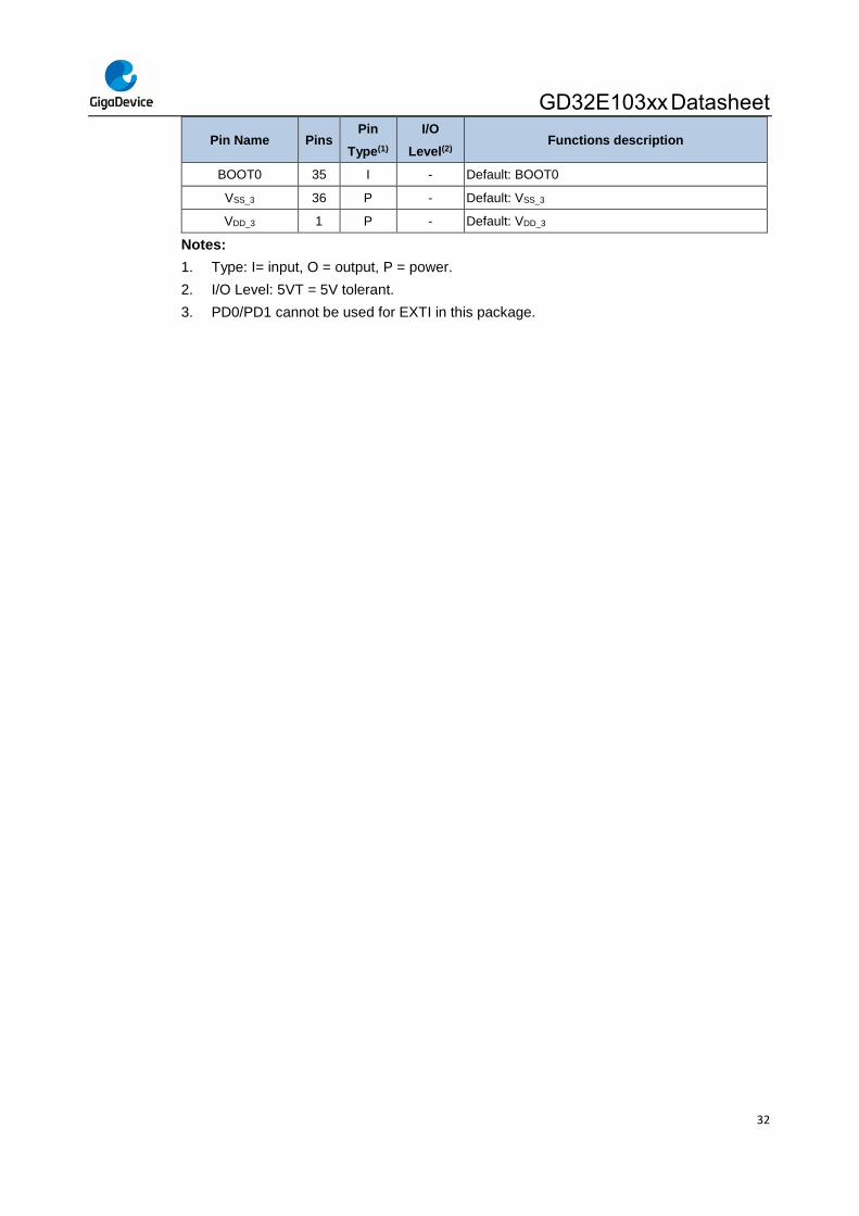
2.6.4. GD32E103Tx QFN36 pin definitions
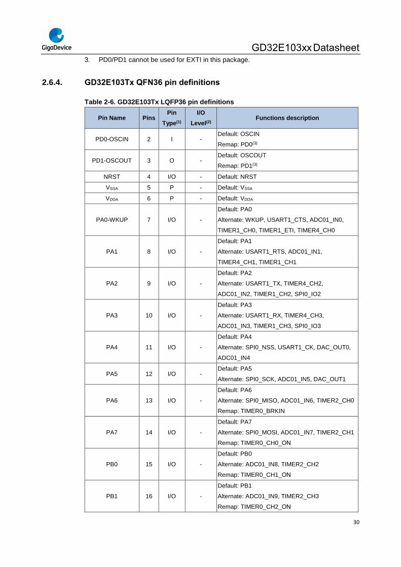
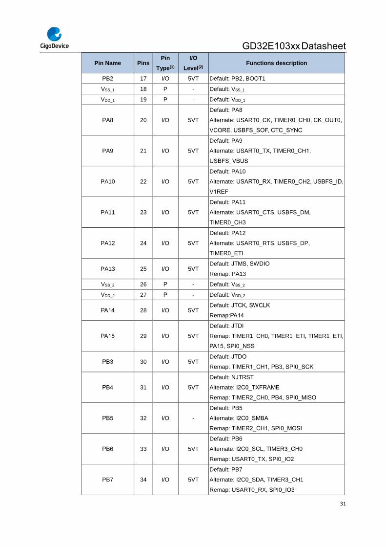
Table 2-6. GD32E103Tx LQFP36 pin definitions
Pin Name Pins Pin
Type(1)
I/O
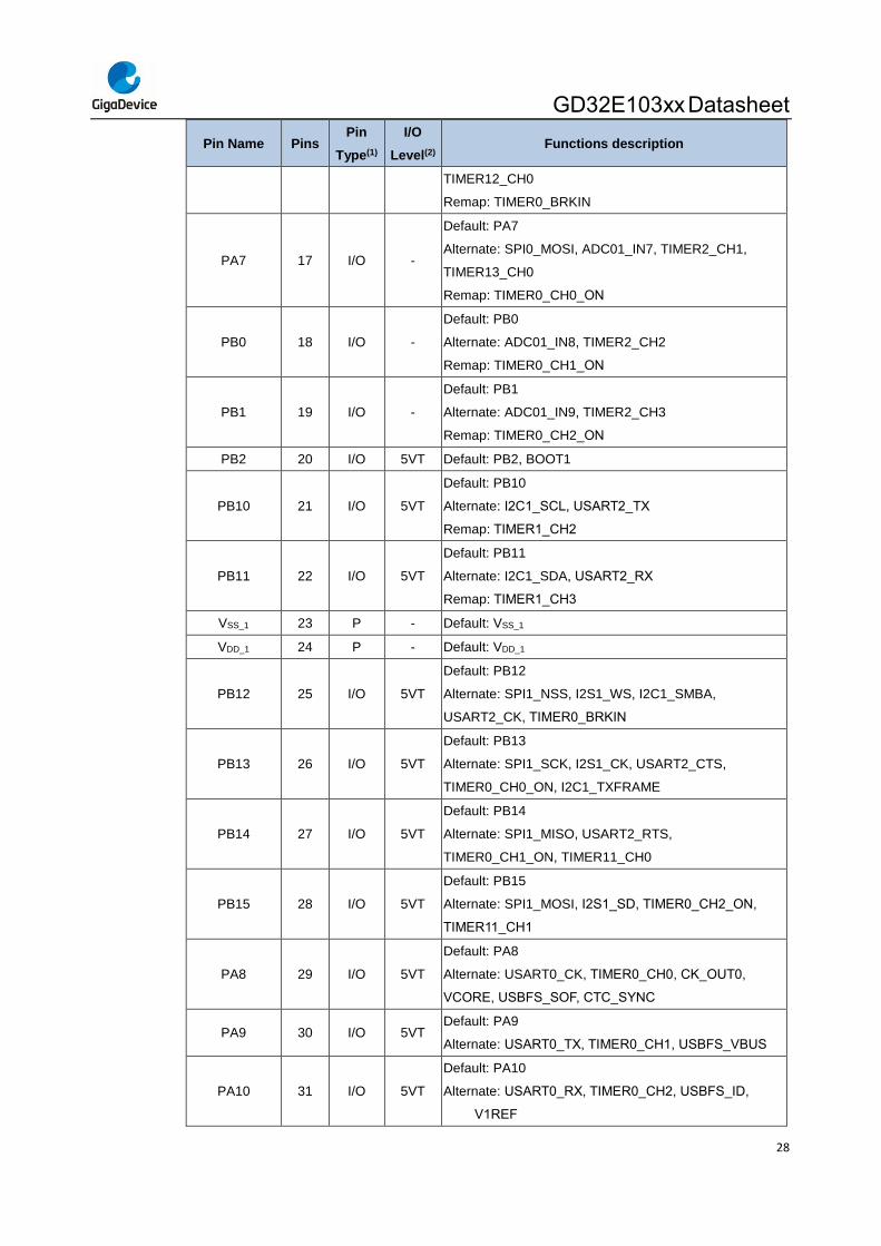
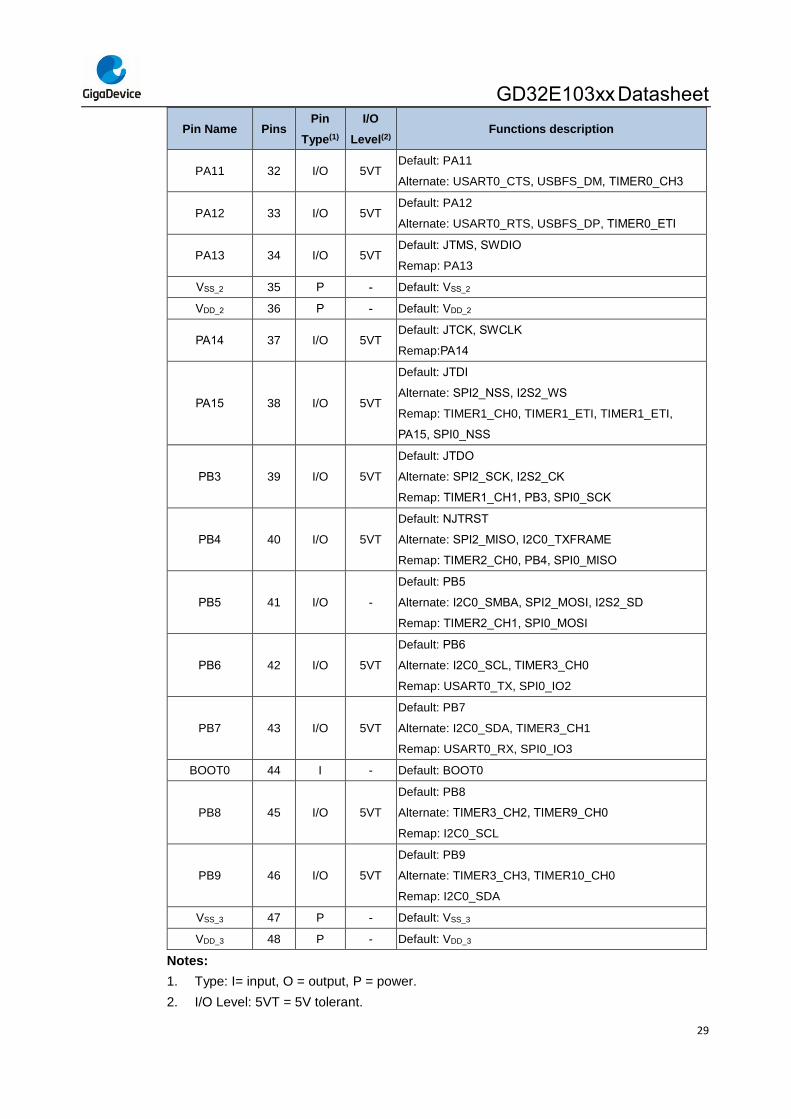
Level(2) Functions description
PD0-OSCIN 2 I - Default: OSCIN
Remap: PD0(3)
PD1-OSCOUT 3 O - Default: OSCOUT
Remap: PD1(3)
NRST 4 I/O - Default: NRST
VSSA 5 P - Default: VSSA
VDDA 6 P - Default: VDDA
PA0-WKUP 7 I/O -
Default: PA0
Alternate: WKUP, USART1_CTS, ADC01_IN0,
TIMER1_CH0, TIMER1_ETI, TIMER4_CH0
PA1 8 I/O -
Default: PA1
Alternate: USART1_RTS, ADC01_IN1,
TIMER4_CH1, TIMER1_CH1
PA2 9 I/O -
Default: PA2
Alternate: USART1_TX, TIMER4_CH2,
ADC01_IN2, TIMER1_CH2, SPI0_IO2
PA3 10 I/O -
Default: PA3
Alternate: USART1_RX, TIMER4_CH3,
ADC01_IN3, TIMER1_CH3, SPI0_IO3
PA4 11 I/O -
Default: PA4
Alternate: SPI0_NSS, USART1_CK, DAC_OUT0,
ADC01_IN4
PA5 12 I/O - Default: PA5
Alternate: SPI0_SCK, ADC01_IN5, DAC_OUT1
PA6 13 I/O -
Default: PA6
Alternate: SPI0_MISO, ADC01_IN6, TIMER2_CH0
Remap: TIMER0_BRKIN
PA7 14 I/O -
Default: PA7
Alternate: SPI0_MOSI, ADC01_IN7, TIMER2_CH1
Remap: TIMER0_CH0_ON
PB0 15 I/O -
Default: PB0
Alternate: ADC01_IN8, TIMER2_CH2
Remap: TIMER0_CH1_ON
PB1 16 I/O -
Default: PB1
Alternate: ADC01_IN9, TIMER2_CH3
Remap: TIMER0_CH2_ON
GD32E103xx Datasheet
31
Pin Name Pins Pin
Type(1)
I/O
Level(2) Functions description
PB2 17 I/O 5VT Default: PB2, BOOT1
VSS_1 18 P - Default: VSS_1
VDD_1 19 P - Default: VDD_1
PA8 20 I/O 5VT
Default: PA8
Alternate: USART0_CK, TIMER0_CH0, CK_OUT0,
VCORE, USBFS_SOF, CTC_SYNC
PA9 21 I/O 5VT
Default: PA9
Alternate: USART0_TX, TIMER0_CH1,
USBFS_VBUS
PA10 22 I/O 5VT
Default: PA10
Alternate: USART0_RX, TIMER0_CH2, USBFS_ID,
V1REF
PA11 23 I/O 5VT
Default: PA11
Alternate: USART0_CTS, USBFS_DM,
TIMER0_CH3
PA12 24 I/O 5VT
Default: PA12
Alternate: USART0_RTS, USBFS_DP,
TIMER0_ETI
PA13 25 I/O 5VT Default: JTMS, SWDIO
Remap: PA13
VSS_2 26 P - Default: VSS_2
VDD_2 27 P - Default: VDD_2
PA14 28 I/O 5VT Default: JTCK, SWCLK
Remap:PA14
PA15 29 I/O 5VT
Default: JTDI
Remap: TIMER1_CH0, TIMER1_ETI, TIMER1_ETI,
PA15, SPI0_NSS
PB3 30 I/O 5VT Default: JTDO
Remap: TIMER1_CH1, PB3, SPI0_SCK
PB4 31 I/O 5VT
Default: NJTRST
Alternate: I2C0_TXFRAME
Remap: TIMER2_CH0, PB4, SPI0_MISO
PB5 32 I/O -
Default: PB5
Alternate: I2C0_SMBA
Remap: TIMER2_CH1, SPI0_MOSI
PB6 33 I/O 5VT
Default: PB6
Alternate: I2C0_SCL, TIMER3_CH0
Remap: USART0_TX, SPI0_IO2
PB7 34 I/O 5VT
Default: PB7
Alternate: I2C0_SDA, TIMER3_CH1
Remap: USART0_RX, SPI0_IO3
GD32E103xx Datasheet
32
Pin Name Pins Pin
Type(1)
I/O
Level(2) Functions description
BOOT0 35 I - Default: BOOT0
VSS_3 36 P - Default: VSS_3
VDD_3 1 P - Default: VDD_3
Notes:
1. Type: I= input, O = output, P = power.
2. I/O Level: 5VT = 5V tolerant.
3. PD0/PD1 cannot be used for EXTI in this package.
GD32E103xx Datasheet
33
3. Functional description
3.1. Arm® Cortex®-M4 core
The Arm® Cortex®-M4 processor is a high performance embedded processor with DSP
instructions which allow efficient signal processing and complex algorithm execution. It brings
an efficient, easy-to-use blend of control and signal processing capabilities to meet the digital
signal control markets demand. The processor is highly configurable enabling a wide range
of implementations from those requiring floating point operations, memory protection and
powerful trace technology to cost sensitive devices requiring minimal area, while delivering
outstanding computational performance and an advanced system response to interrupts.
32-bit Arm® Cortex®-M4 processor core
Up to 120 MHz operation frequency
Single-cycle multiplication and hardware divider
Floating Point Unit (FPU)
Integrated DSP instructions
Integrated Nested Vectored Interrupt Controller (NVIC)
24-bit SysTick timer
The Cortex®-M4 processor is based on the ARMv7-M architecture and supports both Thumb
and Thumb-2 instruction sets. Some system peripherals listed below are also provided by
Cortex®-M4:
Internal Bus Matrix connected with ICode bus, DCode bus, system bus, Private Peripheral
Bus (PPB) and debug accesses (AHB-AP)
Nested Vectored Interrupt Controller (NVIC)
Flash Patch and Breakpoint (FPB)
Data Watchpoint and Trace (DWT)
Instrument Trace Macrocell (ITM)
Serial Wire JTAG Debug Port (SWJ-DP)
Trace Port Interface Unit (TPIU)
3.2. On-chip memory
Up to 128 Kbytes of Flash memory
Up to 32 KB of SRAM
The Arm® Cortex®-M4 processor is structured in Harvard architecture which can use separate
buses to fetch instructions and load/store data. 128 Kbytes of inner Flash at most, which
includes code Flash that available for storing programs and data, and accessed (R/W) at CPU
clock speed. An extra data Flash is also included for storing data mainly. Table 2-2.
GD32E103xx memory map shows the memory of the GD32E103xx series of devices,
including Flash, SRAM, peripheral, and other pre-defined regions.
GD32E103xx Datasheet
34
3.3. Clock, reset and supply management
Internal 8 MHz factory-trimmed RC and external 4 to 32 MHz crystal oscillator
Internal 48 MHz RC oscillator
Internal 40 KHz RC calibrated oscillator and external 32.768 KHz crystal oscillator
1.71 to 3.6 V application supply and I/Os
Supply Supervisor: POR (Power On Reset), PDR (Power Down Reset), and low voltage
detector (LVD)
The Clock Control Unit (CCU) provides a range of oscillator and clock functions. These
include internal RC oscillator and external crystal oscillator, high speed and low speed two
types. Several prescalers allow the frequency configuration of the AHB and two APB domains.
The maximum frequency of the two AHB domains are 120MHz. The maximum frequency of
the two APB domains including APB1 is 60 MHz and APB2 is 120 MHz. See Figure 2-6.
GD32E103xx clock tree for details on the clock tree.
The Reset Control Unit (RCU) controls three kinds of reset: system reset resets the processor
core and peripheral IP components. Power-on reset (POR) and power-down reset (PDR) are
always active, and ensures proper operation starting from 1.66V/down to 1.62V. The device
remains in reset mode when VDD is below a specified threshold. The embedded low voltage
detector (LVD) monitors the power supply, compares it to the voltage threshold and generates
an interrupt as a warning message for leading the MCU into security.
Power supply schemes:
VDD range: 1.71 to 3.6 V, external power supply for I/Os and the internal regulator.
Provided externally through VDD pins.
VDDA range: 1.71 to 3.6 V, external analog power supplies for ADC, reset blocks, RCs and
PLL VDDA and VSSA must be connected to VDD and VSS, respectively.
VBAT range: 1.71 to 3.6 V, power supply for RTC, external clock 32.768 KHz oscillator and
backup registers (through power switch) when VDD is not present.
3.4. Boot modes
At startup, boot pins are used to select one of three boot options:
Boot from main flash memory (default)
Boot from system memory
Boot from on-chip SRAM
In default condition, boot from main Flash memory is selected. The boot loader is located in
the internal boot ROM memory (system memory). It is used to reprogram the Flash memory
by using USART0 (PA9 and PA10).
GD32E103xx Datasheet
35
3.5. Power saving modes
The MCU supports three kinds of power saving modes to achieve even lower power
consumption. They are Sleep mode, Deep-sleep mode, and Standby mode. These operating
modes reduce the power consumption and allow the application to achieve the best balance
between the CPU operating time, speed and power consumption.
Sleep mode
In sleep mode, only the clock of CPU core is off. All peripherals continue to operate and
any interrupt/event can wake up the system.
Deep-sleep mode
In deep-sleep mode, all clocks in the 1.2V domain are off, and all of the high speed
crystal oscillator (IRC8M, IRC48M, HXTAL) and PLL are disabled. Only the contents of
SRAM and registers are retained. Any interrupt or wakeup event from EXTI lines can
wake up the system from the deep-sleep mode including the 16 external lines, the RTC
alarm, the LVD output, and USB wakeup. When exiting the deep-sleep mode, the IRC8M
is selected as the system clock.
Standby mode
In standby mode, the whole 1.2V domain is power off, the LDO is shut down, and all of
IRC8M, IRC48M, HXTAL and PLL are disabled. The contents of SRAM and registers
(except Backup Registers) are lost. There are four wakeup sources for the standby mode,
including the external reset from NRST pin, the RTC, the FWDG reset, and the rising
edge on WKUP pin.
3.6. Analog to digital converter (ADC)
12-bit SAR ADC's conversion rate is up to 3 MSPS
12-bit, 10-bit, 8-bit or 6-bit configurable resolution
Hardware oversampling ratio adjustable from 2 to 256x improves resolution to 16-bit
Input voltage range: VREF- to VREF+
Temperature sensor
Up to two 12-bit 3 MSPS multi-channel ADCs are integrated in the device. It has a total of 18
multiplexed channels: 16 external channels, 1 channel for internal temperature sensor
(VSENSE), 1 channel for internal reference voltage (VREFINT, VREFINT = 1.2V). The input voltage
range is from VREF- to VREF+. An on-chip hardware oversampling scheme improves
performance while off-loading the related computational burden from the CPU. An analog
watchdog block can be used to detect the channels, which are required to remain within a
specific threshold window. A configurable channel management block can be used to perform
conversions in single, continuous, scan or discontinuous mode to support more advanced
use.
The ADC can be triggered from the events generated by the general level 0 timers (TIMERx,
x=1, 2, 3) and the advanced timers (TIMER0 and TIMER7) with internal connection. The
GD32E103xx Datasheet
36
temperature sensor can be used to generate a voltage that varies linearly with temperature.
It is internally connected to the ADC_IN16 input channel which is used to convert the sensor
output voltage in a digital value.
3.7. Digital to analog converter (DAC)
12-bit DAC with independent output channels
8-bit or 12-bit mode in conjunction with the DMA controller
The 12-bit buffered DAC is used to generate variable analog outputs. The DAC channels can
be triggered by the timer or EXTI with DMA support. In dual DAC channel operation,
conversions could be done independently or simultaneously. The maximum output value of
the DAC is VREF+.
3.8. DMA
7 channel DMA0 controller and 5 channel DMA1 controller
Peripherals supported: Timers, ADC, SPIs, I2Cs, USARTs, DAC, I2S
The flexible general-purpose DMA controllers provide a hardware method of transferring data
between peripherals and/or memory without intervention from the CPU, thereby freeing up
bandwidth for other system functions. Three types of access method are supported:
peripheral to memory, memory to peripheral, memory to memory.
Each channel is connected to fixed hardware DMA requests. The priorities of DMA channel
requests are determined by software configuration and hardware channel number. Transfer
size of source and destination are independent and configurable.
3.9. General-purpose inputs/outputs (GPIOs)
Up to 80 fast GPIOs, all mappable on 16 external interrupt lines
Analog input/output configurable
Alternate function input/output configurable
There are up to 80 general purpose I/O pins (GPIO) in GD32E103xx, named PA0 ~ PA15,
PB0 ~ PB15, PC0 ~ PC15, PD0 ~ PD15 and PE0 ~ PE15 to implement logic input/output
functions. Each of the GPIO ports has related control and configuration registers to satisfy
the requirements of specific applications. The external interrupts on the GPIO pins of the
device have related control and configuration registers in the Interrupt/event controller (EXTI).
The GPIO ports are pin-shared with other alternative functions (AFs) to obtain maximum
flexibility on the package pins. Each of the GPIO pins can be configured by software as output
(push-pull or open-drain), as input (with or without pull-up or pull-down) or as peripheral
alternate function. Most of the GPIO pins are shared with digital or analog alternate functions.
All GPIOs are high-current capable except for analog inputs.
GD32E103xx Datasheet
37
3.10. Timers and PWM generation
Two 16-bit advanced timer (TIMER0 & TIMER7), ten 16-bit general timers (TIMER1 ~
TIMER4, TIMER8 ~ TIMER13), and two 16-bit basic timer (TIMER5 & TIMER6)
Up to 4 independent channels of PWM, output compare or input capture for each general
timer and external trigger input
16-bit, motor control PWM advanced timer with programmable dead-time generation for
output match
Encoder interface controller with two inputs using quadrature decoder
24-bit SysTick timer down counter
2 watchdog timers (free watchdog timer and window watchdog timer)
The advanced timer (TIMER0 & TIMER7) can be used as a three-phase PWM multiplexed
on 6 channels. It has complementary PWM outputs with programmable dead-time generation.
It can also be used as a complete general timer. The 4 independent channels can be used
for input capture, output compare, PWM generation (edge-aligned or center-aligned counting
modes) and single pulse mode output. If configured as a general 16-bit timer, it has the same
functions as the TIMERx timer. It can be synchronized with external signals or to interconnect
with other general timers together which have the same architecture and features.
The general timer, can be used for a variety of purposes including general time, input signal
pulse width measurement or output waveform generation such as a single pulse generation
or PWM output, up to 4 independent channels for input capture/output compare. TIMER1 ~
TIMER4 is based on a 16-bit auto-reload up/downcounter and a 16-bit prescaler. TIMER8 ~
TIMER13 is based on a 16-bit auto-reload upcounter and a 16-bit prescaler. The general timer
also supports an encoder interface with two inputs using quadrature decoder.
The basic timer, known as TIMER5 &TIMER6, are mainly used for DAC trigger generation.
They can also be used as a simple 16-bit time base.
The GD32E103xx have two watchdog peripherals, free watchdog timer and window watchdog
timer. They offer a combination of high safety level, flexibility of use and timing accuracy.
The free watchdog timer includes a 12-bit down-counting counter and an 8-bit prescaler. It is
clocked from an independent 40 KHz internal RC and as it operates independently of the
main clock, it can operate in deep-sleep and standby modes. It can be used either as a
watchdog to reset the device when a problem occurs, or as a free-running timer for application
timeout management.
The window watchdog timer is based on a 7-bit down counter that can be set as free-running.
It can be used as a watchdog to reset the device when a problem occurs. It is clocked from
the main clock. It has an early wakeup interrupt capability and the counter can be frozen in
debug mode.
The SysTick timer is dedicated for OS, but could also be used as a standard down counter.
It features:
GD32E103xx Datasheet
38
A 24-bit down counter
Auto reload capability
Maskable system interrupt generation when the counter reaches 0
Programmable clock source
3.11. Real time clock (RTC)
32-bit up-counter with a programmable 20-bit prescaler
Alarm function
Interrupt and wake-up event
The real time clock is an independent timer which provides a set of continuously running
counters which can be used with suitable software to provide a clock calendar function, and
provides an alarm interrupt and an expected interrupt. The RTC features a 32-bit
programmable counter for long-term measurement using the compare register to generate an
alarm. A 20-bit prescaler is used for the time base clock and is by default configured to
generate a time base of 1 second from a clock at 32.768 KHz from external crystal oscillator.
3.12. Inter-integrated circuit (I2C)
Up to two I2C bus interfaces can support both master and slave mode with a frequency
up to 1 MHz (Fast mode plus)
Provide arbitration function, optional PEC (packet error checking) generation and
checking
Supports 7-bit and 10-bit addressing mode and general call addressing mode
The I2C interface is an internal circuit allowing communication with an external I2C interface
which is an industry standard two line serial interface used for connection to external
hardware. These two serial lines are known as a serial data line (SDA) and a serial clock line
(SCL). The I2C module provides several data transfer rates: up to 100 KHz of standard mode,
up to 400 KHz of the fast mode and up to 1 MHz of the fast mode plus. The I2C module also
has an arbitration detect function to prevent the situation where more than one master
attempts to transmit data to the I2C bus at the same time. A CRC-8 calculator is also provided
in I2C interface to perform packet error checking for I2C data.
3.13. Serial peripheral interface (SPI)
Up to three SPI interfaces with a frequency of up to 30 MHz
Support both master and slave mode
Hardware CRC calculation and transmit automatic CRC error checking
Quad-SPI configuration available in master mode (only in SPI0)
SPI TI mode and NSS pulse mode supported
GD32E103xx Datasheet
39
The SPI interface uses 4 pins, among which are the serial data input and output lines (MISO
& MOSI), the clock line (SCK) and the slave select line (NSS). Both SPIs can be served by
the DMA controller. The SPI interface may be used for a variety of purposes, including simplex
synchronous transfers on two lines with a possible bidirectional data line or reliable
communication using CRC checking.
3.14. Universal synchronous asynchronous receiver transmitter
(USART)
Up to three USARTs and two UARTs with operating frequency up to 7.5MBits/s
Supports both asynchronous and clocked synchronous serial communication modes
IrDA SIR encoder and decoder support
LIN break generation and detection
USARTs support ISO 7816-3 compliant smart card interface
The USART (USART0, USART1 and USART2) and UART (UART3 & UART4) are used to
translate data between parallel and serial interfaces, provides a flexible full duplex data
exchange using synchronous or asynchronous transfer. It is also commonly used for RS-232
standard communication. The USART/UART includes a programmable baud rate generator
which is capable of dividing the system clock to produce a dedicated clock for the USART
transmitter and receiver. The USART/UART also supports DMA function for high speed data
communication except UART4.
3.15. Inter-IC sound (I2S)
Two I2S bus interfaces with sampling frequency from 8 KHz to 192 KHz
Support either master or slave mode
The Inter-IC sound (I2S) bus provides a standard communication interface for digital audio
applications by 3-wire serial lines. GD32E103xx contain two I2S-bus interfaces that can be
operated with 16/32 bit resolution in master or slave mode, pin multiplexed with SPI1 and
SPI2. The audio sampling frequency from 8 KHz to 192 KHz is supported.
3.16. Universal serial bus full-speed interface (USBFS)
One full-speed USB Interface with frequency up to 12 Mbit/s
Internal 48 MHz oscillator support crystal-less operation
Internal main PLL for USB CLK compliantly
The Universal Serial Bus (USB) is a 4-wire bus with 4 bidirectional endpoints. The device
controller enables 12 Mbit/s data exchange with integrated transceivers. Transaction
formatting is performed by the hardware, including CRC generation and checking. It supports
GD32E103xx Datasheet
40
device modes. The status of a completed USB transfer or error condition is indicated by status
registers. An interrupt is also generated if enabled. The required precise 48 MHz clock which
can be generated from the internal main PLL (the clock source must use an HXTAL crystal
oscillator) or by the internal 48 MHz oscillator in automatic trimming mode that allows crystal-
less operation.
3.17. External memory controller (EXMC)
Supported external memory: SRAM, PSRAM, ROM and NOR-Flash
Up to 16-bit data bus
Support to interface with Motorola 6800 and Intel 8080 type LCD directly
External memory controller (EXMC) is an abbreviation of external memory controller. It is
divided in to several sub-banks for external device support, each sub-bank has its own chip
selection signal but at one time, only one bank can be accessed. The EXMC support code
execution from external memory. The EXMC also can be configured to interface with the most
common LCD module of Motorola 6800 and Intel 8080 series and reduce the system cost
and complexity.
3.18. Debug mode
Serial wire JTAG debug port (SWJ-DP)
The Arm® SWJ-DP Interface is embedded and is a combined JTAG and serial wire debug
port that enables either a serial wire debug or a JTAG probe to be connected to the target.
3.19. Package and operation temperature
LQFP100 (GD32E103Vx), LQFP64 (GD32E103Rx) and LQFP48 (GD32E103Cx) QFN36
(GD32E103Tx)
Operation temperature range: -40°C to +85°C (industrial level)
GD32E103xx Datasheet
41
4. Electrical characteristics
4.1. Absolute maximum ratings
The maximum ratings are the limits to which the device can be subjected without permanently
damaging the device. Note that the device is not guaranteed to operate properly at the
maximum ratings. Exposure to the absolute maximum rating conditions for extended periods
may affect device reliability.
Table 4-1. Absolute maximum ratings(1)(4)
Symbol Parameter Min Max Unit
VDD External voltage range(2) VSS - 0.3 VSS + 3.6 V
VDDA External analog supply voltage VSSA - 0.3 VSSA + 3.6 V
VBAT External battery supply voltage VSS - 0.3 VSS + 3.6 V
VIN Input voltage on 5V tolerant pin(3) VSS - 0.3 VDD + 3.6 V
Input voltage on other I/O VSS - 0.3 3.6 V
|ΔVDDX| Variations between different VDD power pins — 50 mV
|VSSX −VSS| Variations between different ground pins — 50 mV
IIO Maximum current for GPIO pins — ±25 mA
TA Operating temperature range -40 +85 °C
PD
Power dissipation at TA = 85°C of LQFP100 — 813
mW Power dissipation at TA = 85°C of LQFP64 — 733
Power dissipation at TA = 85°C of LQFP48 — 574
Power dissipation at TA = 85°C of QFN36 — 1086
TSTG Storage temperature range -65 +150 °C
TJ Maximum junction temperature — 125 °C
(1) Guaranteed by design, not tested in production.
(2) All main power and ground pins should be connected to an external power source within the allowable range.
(3) VIN maximum value cannot exceed 5.5 V.
(4) It is recommended that VDD and VDDA are powered by the same source. The maximum difference between VDD
and VDDA does not exceed 300 mV during power-up and operation.
4.2. Operating conditions characteristics
Table 4-2. DC operating conditions
Symbol Parameter Conditions Min(1) Typ Max(1) Unit
VDD Supply voltage — 1.71 3.3 3.6 V
VDDA Analog supply voltage ADC not used
— 1.71 3.3 3.6
V Analog supply voltage ADC used 2.4 3.3 3.6
VBAT Battery supply voltage — 1.71 — 3.6 V
(1) Guaranteed by design, not tested in production.
Figure 4-1. Recommended power supply decoupling capacitors(1)(2)
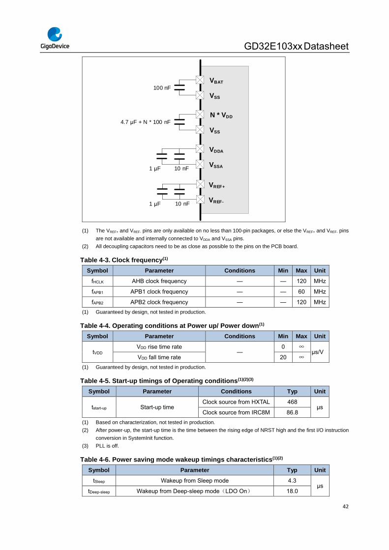
GD32E103xx Datasheet
42
100 nF
VBAT
VSS
N * VDD
VSS
4.7 μF + N * 100 nF
10 nF
VDDA
VSSA1 μF
10 nF
VREF+
VREF-1 μF
(1) The VREF+ and VREF- pins are only available on no less than 100-pin packages, or else the VREF+ and VREF- pins
are not available and internally connected to VDDA and VSSA pins.
(2) All decoupling capacitors need to be as close as possible to the pins on the PCB board.
Table 4-3. Clock frequency(1)
Symbol Parameter Conditions Min Max Unit
fHCLK AHB clock frequency — — 120 MHz
fAPB1 APB1 clock frequency — — 60 MHz
fAPB2 APB2 clock frequency — — 120 MHz
(1) Guaranteed by design, not tested in production.
Table 4-4. Operating conditions at Power up/ Power down(1)
Symbol Parameter Conditions Min Max Unit
tVDD VDD rise time rate
— 0 ∞
μs/V VDD fall time rate 20 ∞
(1) Guaranteed by design, not tested in production.
Table 4-5. Start-up timings of Operating conditions(1)(2)(3)
Symbol Parameter Conditions Typ Unit
tstart-up Start-up time Clock source from HXTAL 468
μs Clock source from IRC8M 86.8
(1) Based on characterization, not tested in production.
(2) After power-up, the start-up time is the time between the rising edge of NRST high and the first I/O instruction
conversion in SystemInit function.
(3) PLL is off.
Table 4-6. Power saving mode wakeup timings characteristics(1)(2)
Symbol Parameter Typ Unit
tSleep Wakeup from Sleep mode 4.3 μs
tDeep-sleep Wakeup from Deep-sleep mode(LDO On) 18.0
GD32E103xx Datasheet
43
Symbol Parameter Typ Unit
Wakeup from Deep-sleep mode(LDO in low power
mode) 18.0
tStandby Wakeup from Standby mode 82.0
(1) Based on characterization, not tested in production.
(2) The wakeup time is measured from the wakeup event to the point at which the application code reads the first
instruction under the below conditions: VDD = VDDA = 3.3 V, IRC8M = System clock = 8 MHz.
4.3. Power consumption
The power measurements specified in the tables represent that code with data executing from
on-chip Flash with the following specifications.
Table 4-7. Power consumption characteristics(2)(3)(4)(5)
Symbol Parameter Conditions Min Typ(1) Max Unit
IDD+IDDA Supply current
(Run mode)
VDD = VDDA = 3.3 V, HXTAL = 25 MHz,
System clock=120 MHz, All peripherals
enabled
— 28.1 — mA
VDD = VDDA = 3.3 V, HXTAL = 25 MHz,
System clock = 120 MHz, All peripherals
disabled
— 16.0 — mA
VDD = VDDA = 3.3 V, HXTAL = 25 MHz,
System clock = 108 MHz, All peripherals
enabled
— 24.6 — mA
VDD = VDDA = 3.3 V, HXTAL = 25 MHz,
System clock = 108 MHz, All peripherals
disabled
— 14.7 — mA
VDD = VDDA = 3.3 V, HXTAL = 25 MHz,
System clock = 96 MHz, All peripherals
enabled
— 22.3 — mA
VDD = VDDA = 3.3 V, HXTAL = 25 MHz,
System clock = 96 MHz, All peripherals
disabled
— 13.6 — mA
VDD = VDDA = 3.3 V, HXTAL = 25 MHz,
System clock = 72 MHz, All peripherals
enabled
— 17.2 — mA
VDD = VDDA = 3.3 V, HXTAL = 25 MHz,
System clock = 72 MHz, All peripherals
disabled
— 10.8 — mA
VDD = VDDA = 3.3 V, HXTAL = 25 MHz,
System clock = 48 MHz, All peripherals
enabled
— 12.3 — mA
VDD = VDDA = 3.3 V, HXTAL = 25 MHz,
System clock = 48 MHz, All peripherals
disabled
— 8.1 — mA
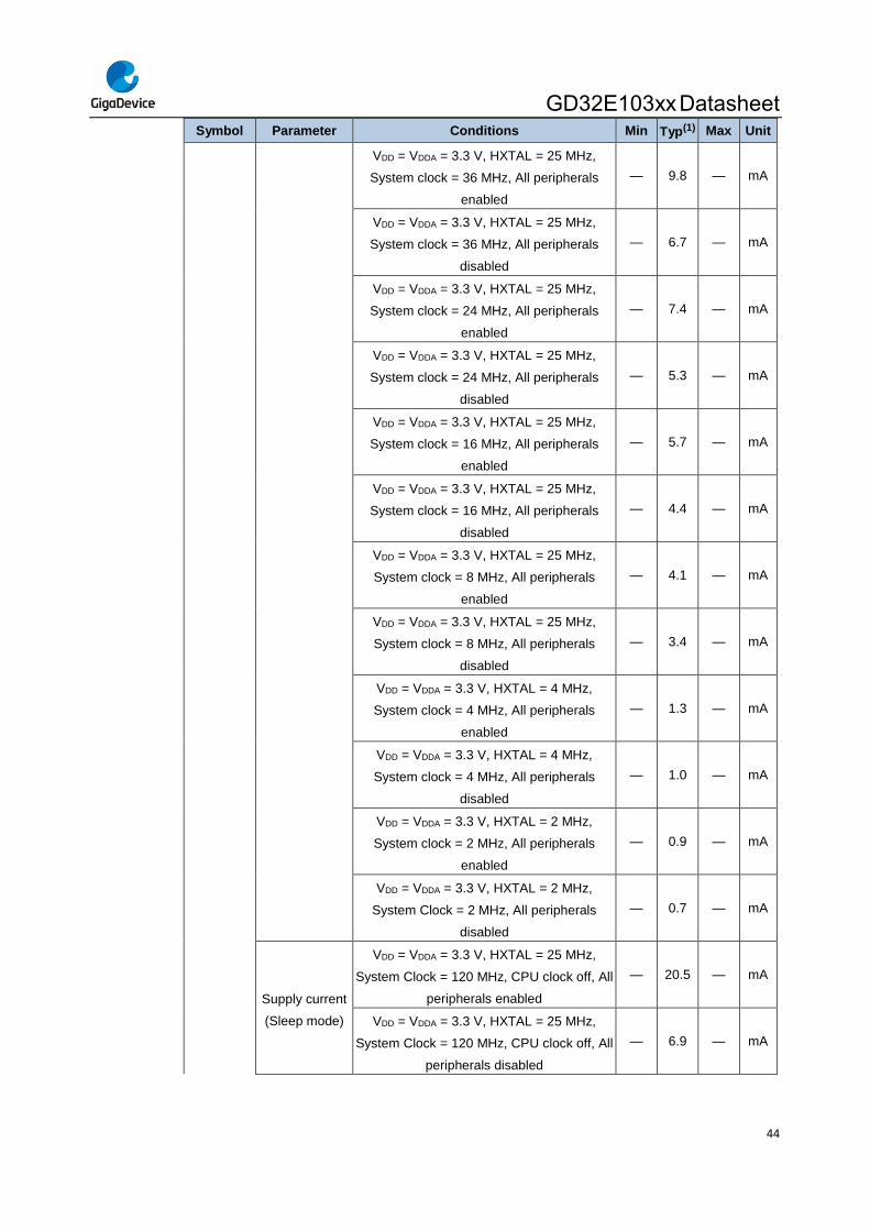
GD32E103xx Datasheet
44
Symbol Parameter Conditions Min Typ(1) Max Unit
VDD = VDDA = 3.3 V, HXTAL = 25 MHz,
System clock = 36 MHz, All peripherals
enabled
— 9.8 — mA
VDD = VDDA = 3.3 V, HXTAL = 25 MHz,
System clock = 36 MHz, All peripherals
disabled
— 6.7 — mA
VDD = VDDA = 3.3 V, HXTAL = 25 MHz,
System clock = 24 MHz, All peripherals
enabled
— 7.4 — mA
VDD = VDDA = 3.3 V, HXTAL = 25 MHz,
System clock = 24 MHz, All peripherals
disabled
— 5.3 — mA
VDD = VDDA = 3.3 V, HXTAL = 25 MHz,
System clock = 16 MHz, All peripherals
enabled
— 5.7 — mA
VDD = VDDA = 3.3 V, HXTAL = 25 MHz,
System clock = 16 MHz, All peripherals
disabled
— 4.4 — mA
VDD = VDDA = 3.3 V, HXTAL = 25 MHz,
System clock = 8 MHz, All peripherals
enabled
— 4.1 — mA
VDD = VDDA = 3.3 V, HXTAL = 25 MHz,
System clock = 8 MHz, All peripherals
disabled
— 3.4 — mA
VDD = VDDA = 3.3 V, HXTAL = 4 MHz,
System clock = 4 MHz, All peripherals
enabled
— 1.3 — mA
VDD = VDDA = 3.3 V, HXTAL = 4 MHz,
System clock = 4 MHz, All peripherals
disabled
— 1.0 — mA
VDD = VDDA = 3.3 V, HXTAL = 2 MHz,
System clock = 2 MHz, All peripherals
enabled
— 0.9 — mA
VDD = VDDA = 3.3 V, HXTAL = 2 MHz,
System Clock = 2 MHz, All peripherals
disabled
— 0.7 — mA
Supply current
(Sleep mode)
VDD = VDDA = 3.3 V, HXTAL = 25 MHz,
System Clock = 120 MHz, CPU clock off, All
peripherals enabled
— 20.5 — mA
VDD = VDDA = 3.3 V, HXTAL = 25 MHz,
System Clock = 120 MHz, CPU clock off, All
peripherals disabled
— 6.9 — mA
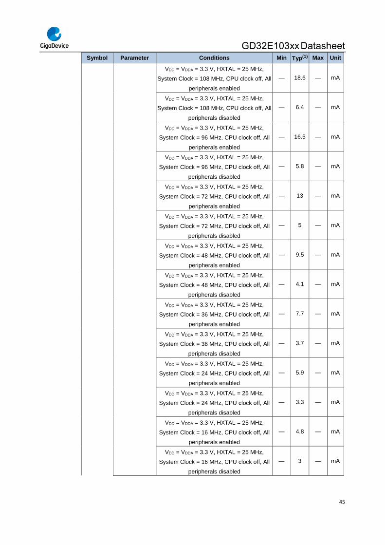
GD32E103xx Datasheet
45
Symbol Parameter Conditions Min Typ(1) Max Unit
VDD = VDDA = 3.3 V, HXTAL = 25 MHz,
System Clock = 108 MHz, CPU clock off, All
peripherals enabled
— 18.6 — mA
VDD = VDDA = 3.3 V, HXTAL = 25 MHz,
System Clock = 108 MHz, CPU clock off, All
peripherals disabled
— 6.4 — mA
VDD = VDDA = 3.3 V, HXTAL = 25 MHz,
System Clock = 96 MHz, CPU clock off, All
peripherals enabled
— 16.5 — mA
VDD = VDDA = 3.3 V, HXTAL = 25 MHz,
System Clock = 96 MHz, CPU clock off, All
peripherals disabled
— 5.8 — mA
VDD = VDDA = 3.3 V, HXTAL = 25 MHz,
System Clock = 72 MHz, CPU clock off, All
peripherals enabled
— 13 — mA
VDD = VDDA = 3.3 V, HXTAL = 25 MHz,
System Clock = 72 MHz, CPU clock off, All
peripherals disabled
— 5 — mA
VDD = VDDA = 3.3 V, HXTAL = 25 MHz,
System Clock = 48 MHz, CPU clock off, All
peripherals enabled
— 9.5 — mA
VDD = VDDA = 3.3 V, HXTAL = 25 MHz,
System Clock = 48 MHz, CPU clock off, All
peripherals disabled
— 4.1 — mA
VDD = VDDA = 3.3 V, HXTAL = 25 MHz,
System Clock = 36 MHz, CPU clock off, All
peripherals enabled
— 7.7 — mA
VDD = VDDA = 3.3 V, HXTAL = 25 MHz,
System Clock = 36 MHz, CPU clock off, All
peripherals disabled
— 3.7 — mA
VDD = VDDA = 3.3 V, HXTAL = 25 MHz,
System Clock = 24 MHz, CPU clock off, All
peripherals enabled
— 5.9 — mA
VDD = VDDA = 3.3 V, HXTAL = 25 MHz,
System Clock = 24 MHz, CPU clock off, All
peripherals disabled
— 3.3 — mA
VDD = VDDA = 3.3 V, HXTAL = 25 MHz,
System Clock = 16 MHz, CPU clock off, All
peripherals enabled
— 4.8 — mA
VDD = VDDA = 3.3 V, HXTAL = 25 MHz,
System Clock = 16 MHz, CPU clock off, All
peripherals disabled
— 3 — mA
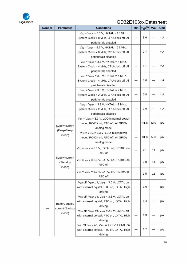
GD32E103xx Datasheet
46
Symbol Parameter Conditions Min Typ(1) Max Unit
VDD = VDDA = 3.3 V, HXTAL = 25 MHz,
System Clock = 8 MHz, CPU clock off, All
peripherals enabled
— 3.6 — mA
VDD = VDDA = 3.3 V, HXTAL = 25 MHz,
System Clock = 8 MHz, CPU clock off, All
peripherals disabled
— 2.7 — mA
VDD = VDDA = 3.3 V, HXTAL = 4 MHz,
System Clock = 4 MHz, CPU clock off, All
peripherals enabled
— 1.1 — mA
VDD = VDDA = 3.3 V, HXTAL = 4 MHz,
System Clock = 4 MHz, CPU clock off, All
peripherals disabled
— 0.6 — mA
VDD = VDDA = 3.3 V, HXTAL = 2 MHz,
System Clock = 2 MHz, CPU clock off, All
peripherals enabled
— 0.8 — mA
VDD = VDDA = 3.3 V, HXTAL = 2 MHz,
System Clock = 2 MHz, CPU clock off, All
peripherals disabled
— 0.6 — mA
Supply current
(Deep-Sleep
mode)
VDD = VDDA = 3.3 V, LDO in normal power
mode, IRC40K off, RTC off, All GPIOs
analog mode
— 41.8 550 μA
VDD = VDDA = 3.3 V, LDO in low power
mode, IRC40K off, RTC off, All GPIOs
analog mode
— 31.8 550 μA
Supply current
(Standby
mode)
VDD = VDDA = 3.3 V, LXTAL off, IRC40K on,
RTC on — 2.1 11 μA
VDD = VDDA = 3.3 V, LXTAL off, IRC40K on,
RTC off — 2.0 11 μA
VDD = VDDA = 3.3 V, LXTAL off, IRC40K off,
RTC off — 1.5 11 μA
IBAT
Battery supply
current (Backup
mode)
VDD off, VDDA off, VBAT = 3.6 V, LXTAL on
with external crystal, RTC on, LXTAL High
driving
— 1.6 — μA
VDD off, VDDA off, VBAT = 3.3 V, LXTAL on
with external crystal, RTC on, LXTAL High
driving
— 1.4 — μA
VDD off, VDDA off, VBAT = 2.5 V, LXTAL on
with external crystal, RTC on, LXTAL High
driving
— 1.3 — μA
VDD off, VDDA off, VBAT = 1.71 V, LXTAL on
with external crystal, RTC on, LXTAL High
driving
— 1.2 — μA
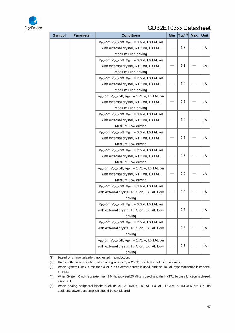
GD32E103xx Datasheet
47
Symbol Parameter Conditions Min Typ(1) Max Unit
VDD off, VDDA off, VBAT = 3.6 V, LXTAL on
with external crystal, RTC on, LXTAL
Medium High driving
— 1.3 — μA
VDD off, VDDA off, VBAT = 3.3 V, LXTAL on
with external crystal, RTC on, LXTAL
Medium High driving
— 1.1 — μA
VDD off, VDDA off, VBAT = 2.5 V, LXTAL on
with external crystal, RTC on, LXTAL
Medium High driving
— 1.0 — μA
VDD off, VDDA off, VBAT = 1.71 V, LXTAL on
with external crystal, RTC on, LXTAL
Medium High driving
— 0.9 — μA
VDD off, VDDA off, VBAT = 3.6 V, LXTAL on
with external crystal, RTC on, LXTAL
Medium Low driving
— 1.0 — μA
VDD off, VDDA off, VBAT = 3.3 V, LXTAL on
with external crystal, RTC on, LXTAL
Medium Low driving
— 0.9 — μA
VDD off, VDDA off, VBAT = 2.5 V, LXTAL on
with external crystal, RTC on, LXTAL
Medium Low driving
— 0.7 — μA
VDD off, VDDA off, VBAT = 1.71 V, LXTAL on
with external crystal, RTC on, LXTAL
Medium Low driving
— 0.6 — μA
VDD off, VDDA off, VBAT = 3.6 V, LXTAL on
with external crystal, RTC on, LXTAL Low
driving
— 0.9 — μA
VDD off, VDDA off, VBAT = 3.3 V, LXTAL on
with external crystal, RTC on, LXTAL Low
driving
— 0.8 — μA
VDD off, VDDA off, VBAT = 2.5 V, LXTAL on
with external crystal, RTC on, LXTAL Low
driving
— 0.6 — μA
VDD off, VDDA off, VBAT = 1.71 V, LXTAL on
with external crystal, RTC on, LXTAL Low
driving
— 0.5 — μA
(1) Based on characterization, not tested in production.
(2) Unless otherwise specified, all values given for TA = 25 ℃ and test result is mean value.
(3) When System Clock is less than 4 MHz, an external source is used, and the HXTAL bypass function is needed,
no PLL.
(4) When System Clock is greater than 8 MHz, a crystal 25 MHz is used, and the HXTAL bypass function is closed,
using PLL.
(5) When analog peripheral blocks such as ADCs, DACs, HXTAL, LXTAL, IRC8M, or IRC40K are ON, an
additionalpower consumption should be considered.
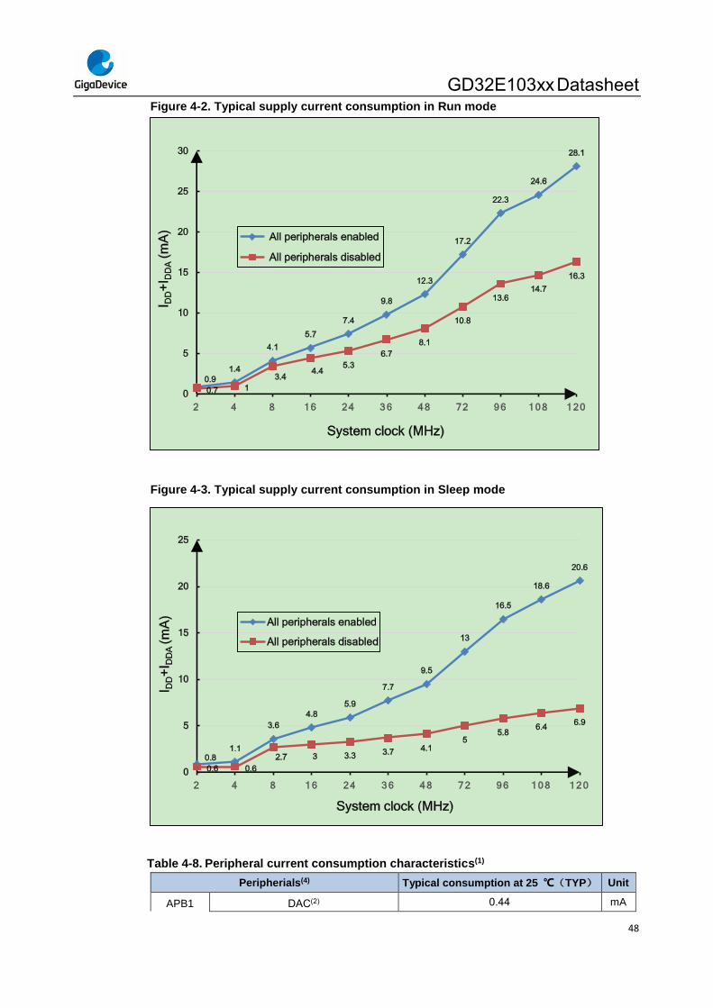
GD32E103xx Datasheet
48
Figure 4-2. Typical supply current consumption in Run mode
Figure 4-3. Typical supply current consumption in Sleep mode
Table 4-8. Peripheral current consumption characteristics(1)
Peripherials(4) Typical consumption at 25 ℃(TYP) Unit
APB1 DAC(2) 0.44 mA
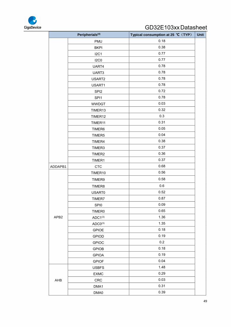
GD32E103xx Datasheet
49
Peripherials(4) Typical consumption at 25 ℃(TYP) Unit
PMU 0.18
BKPI 0.38
I2C1 0.77
I2C0 0.77
UART4 0.78
UART3 0.78
USART2 0.78
USART1 0.78
SPI2 0.72
SPI1 0.78
WWDGT 0.03
TIMER13 0.32
TIMER12 0.3
TIMER11 0.31
TIMER6 0.05
TIMER5 0.04
TIMER4 0.38
TIMER3 0.37
TIMER2 0.36
TIMER1 0.37
ADDAPB1 CTC 0.68
APB2
TIMER10 0.56
TIMER9 0.58
TIMER8 0.6
USART0 0.52
TIMER7 0.87
SPI0 0.09
TIMER0 0.65
ADC1(3) 1.36
ADC0(3) 1.35
GPIOE 0.18
GPIOD 0.19
GPIOC 0.2
GPIOB 0.18
GPIOA 0.19
GPIOF 0.04
AHB
USBFS 1.48
EXMC 0.29
CRC 0.03
DMA1 0.31
DMA0 0.39
GD32E103xx Datasheet
50
(1) Based on characterization, not tested in production.
(2) DEN0 and DEN1 bits in the DAC_CTL register are set to 1, and the converted value set to 0x800.
(3) System clock = fHCLK = 72 MHz, fAPB1 = fHCLK/2, fAPB2 = fHCLK, fADCCLK = fAPB2/2, ADCON bit is set to 1.
(4) If there is no other description, then HXTAL = 25 MHz, system clock = fHCLK = 120 MHz, fAPB1 = fHCLK/2, fAPB2 =
fHCLK.
4.4. EMC characteristics
EMS (electromagnetic susceptibility) includes ESD (Electrostatic discharge, positive and
negative) and FTB (Burst of Fast Transient voltage, positive and negative) testing result is
given in the Table 4-9. EMS characteristics(1), based on the EMS levels and classes
compliant with IEC 61000 series standard.
Table 4-9. EMS characteristics(1)
Symbol Parameter Conditions Level/Class
VESD Voltage applied to all device pins to
induce a functional disturbance
VDD = 3.3 V, TA = 25 °C,
LQFP100, fHCLK = 120 MHz
conforms to IEC 61000-4-2
3A
VFTB
Fast transient voltage burst applied to
induce a functional disturbance through
100 pF on VDD and VSS pins
VDD= 3.3 V, TA = 25 °C,
LQFP100, fHCLK = 120 MHz
conforms to IEC 61000-4-4
4A
(1) Based on characterization, not tested in production.
4.5. Power supply supervisor characteristics
Table 4-10. Power supply supervisor characteristics
Symbol Parameter Conditions Min Typ Max Unit
VLVD(1)
Low voltage
Detector Threshold
LVDT<2:0> = 000(rising edge) — 2.07 —
V
LVDT<2:0> = 000(falling edge) — 1.97 —
LVDT<2:0> = 001(rising edge) — 2.2 —
LVDT<2:0> = 001(falling edge) — 2.1 —
LVDT<2:0> = 010(rising edge) — 2.34 —
LVDT<2:0> = 010(falling edge) — 2.24 —
LVDT<2:0> = 011(rising edge) — 2.47 —
LVDT<2:0> = 011(falling edge) — 2.37 —
LVDT<2:0> = 100(rising edge) — 2.61 —
LVDT<2:0> = 100(falling edge) — 2.51 —
LVDT<2:0> = 101(rising edge) — 2.74 —
GD32E103xx Datasheet
51
Symbol Parameter Conditions Min Typ Max Unit
LVDT<2:0> = 101(falling edge) — 2.64 —
LVDT<2:0> = 110(rising edge) — 2.88 —
LVDT<2:0> = 110(falling edge) — 2.78 —
LVDT<2:0> = 111(rising edge) — 3.01 —
LVDT<2:0> = 111(falling edge) — 2.91 —
VLVDhyst(2) LVD hystersis — — 100 — mV
VPOR(1) Power on reset threshold
—
— 1.67 — V
VPDR(1)
Power down reset
threshold — 1.62 — V
VPDRhyst(2) PDR hysteresis — 40 — mV
tRSTTEMPO(2) Reset temporization — 2 — ms
(1) Based on characterization, not tested in production.
(2) Guaranteed by design, not tested in production.
4.6. Electrical sensitivity
The device is strained in order to determine its performance in terms of electrical sensitivity.
Electrostatic discharges (ESD) are applied directly to the pins of the sample. Static latch-up
(LU) test is based on the two measurement methods.
Table 4-11. ESD characteristics(1)
Symbol Parameter Conditions Min Typ Max Unit
VESD(HBM) Electrostatic discharge
voltage (human body model)
TA = 25 °C;
JS-001-2014 — — 5000 V
VESD(CDM) Electrostatic discharge
voltage (charge device model)
TA = 25 °C;
JS-002-2014 — — 800 V
(1) Based on characterization, not tested in production.
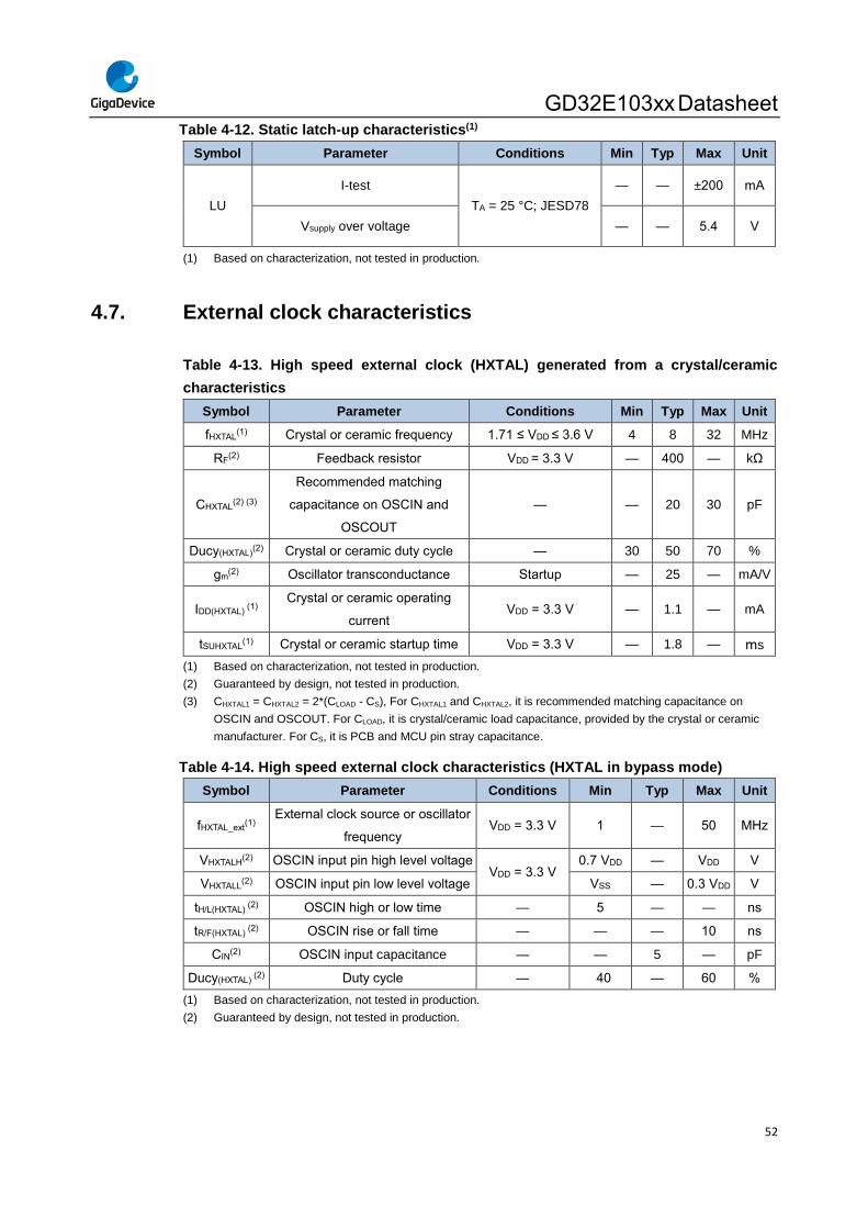
GD32E103xx Datasheet
52
Table 4-12. Static latch-up characteristics(1)
Symbol Parameter Conditions Min Typ Max Unit
LU
I-test
TA = 25 °C; JESD78
— — ±200 mA
Vsupply over voltage — — 5.4 V
(1) Based on characterization, not tested in production.
4.7. External clock characteristics
Table 4-13. High speed external clock (HXTAL) generated from a crystal/ceramic
characteristics
Symbol Parameter Conditions Min Typ Max Unit
fHXTAL(1) Crystal or ceramic frequency 1.71 ≤ VDD ≤ 3.6 V 4 8 32 MHz
RF(2) Feedback resistor VDD = 3.3 V — 400 — kΩ
CHXTAL(2) (3)
Recommended matching
capacitance on OSCIN and
OSCOUT
— — 20 30 pF
Ducy(HXTAL)(2) Crystal or ceramic duty cycle — 30 50 70 %
gm(2) Oscillator transconductance Startup — 25 — mA/V
IDD(HXTAL) (1)
Crystal or ceramic operating
current VDD = 3.3 V — 1.1 — mA
tSUHXTAL(1) Crystal or ceramic startup time VDD = 3.3 V — 1.8 — ms
(1) Based on characterization, not tested in production.
(2) Guaranteed by design, not tested in production.
(3) CHXTAL1 = CHXTAL2 = 2*(CLOAD - CS), For CHXTAL1 and CHXTAL2, it is recommended matching capacitance on
OSCIN and OSCOUT. For CLOAD, it is crystal/ceramic load capacitance, provided by the crystal or ceramic
manufacturer. For CS, it is PCB and MCU pin stray capacitance.
Table 4-14. High speed external clock characteristics (HXTAL in bypass mode)
Symbol Parameter Conditions Min Typ Max Unit
fHXTAL_ext(1)
External clock source or oscillator
frequency VDD = 3.3 V 1 — 50 MHz
VHXTALH(2) OSCIN input pin high level voltage
VDD = 3.3 V 0.7 VDD — VDD V
VHXTALL(2) OSCIN input pin low level voltage VSS — 0.3 VDD V
tH/L(HXTAL) (2) OSCIN high or low time — 5 — — ns
tR/F(HXTAL) (2) OSCIN rise or fall time — — — 10 ns
CIN(2) OSCIN input capacitance — — 5 — pF
Ducy(HXTAL) (2) Duty cycle — 40 — 60 %
(1) Based on characterization, not tested in production.
(2) Guaranteed by design, not tested in production.
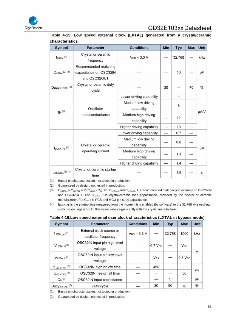
GD32E103xx Datasheet
53
Table 4-15. Low speed external clock (LXTAL) generated from a crystal/ceramic
characteristics
Symbol Parameter Conditions Min Typ Max Unit
fLXTAL(1)
Crystal or ceramic
frequency VDD = 3.3 V — 32.768 — kHz
CLXTAL(2) (3)
Recommended matching
capacitance on OSC32IN
and OSC32OUT
— — 10 — pF
Ducy(LXTAL) (2)
Crystal or ceramic duty
cycle — 30 — 70 %
gm(2)
Oscillator
transconductance
Lower driving capability — 4 —
μA/V
Medium low driving
capability — 6 —
Medium high driving
capability — 12 —
Higher driving capability — 18 —
IDDLXTAL (1)
Crystal or ceramic
operating current
Lower driving capability — 0.7 —
μA
Medium low driving
capability — 0.8 —
Medium high driving
capability — 1.1 —
Higher driving capability — 1.4 —
tSULXTAL(1) (4)
Crystal or ceramic startup
time — — 1.8 — s
(1) Based on characterization, not tested in production.
(2) Guaranteed by design, not tested in production.
(3) CLXTAL1 = CLXTAL2 = 2*(CLOAD - CS), For CLXTAL1 and CLXTAL2, it is recommended matching capacitance on OSC32IN
and OSC32OUT. For CLOAD, it is crystal/ceramic load capacitance, provided by the crystal or ceramic
manufacturer. For CS, it is PCB and MCU pin stray capacitance.
(4) tSULXTAL is the startup time measured from the moment it is enabled (by software) to the 32.768 kHz oscillator
stabilization flags is SET. This value varies significantly with the crystal manufacturer.
Table 4-16.Low speed external user clock characteristics (LXTAL in bypass mode)
Symbol Parameter Conditions Min Typ Max Unit
fLXTAL_ext(1)
External clock source or
oscillator frequency VDD = 3.3 V — 32.768 1000 kHz
VLXTALH(2)
OSC32IN input pin high level
voltage — 0.7 VDD — VDD
V
VLXTALL(2)
OSC32IN input pin low level
voltage — VSS — 0.3 VDD
tH/L(LXTAL) (2)
OSC32IN high or low time — 450 — — ns
tR/F(LXTAL) (2)
OSC32IN rise or fall time — — — 50
CIN(2) OSC32IN input capacitance — — 5 — pF
Ducy(LXTAL) (2) Duty cycle — 30 50 70 %
(1) Based on characterization, not tested in production.
(2) Guaranteed by design, not tested in production.
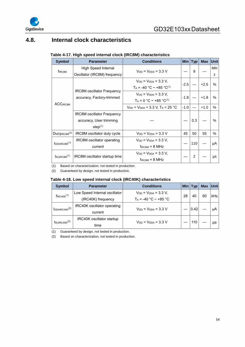
GD32E103xx Datasheet
54
4.8. Internal clock characteristics
Table 4-17. High speed internal clock (IRC8M) characteristics
Symbol Parameter Conditions Min Typ Max Unit
fIRC8M High Speed Internal
Oscillator (IRC8M) frequency VDD = VDDA = 3.3 V — 8 —
MH
z
ACCIRC8M
IRC8M oscillator Frequency
accuracy, Factory-trimmed
VDD = VDDA = 3.3 V,
TA = -40 °C ~ +85 °C(1) -2.5 — +2.5 %
VDD = VDDA = 3.3 V,
TA = 0 °C ~ +85 °C(1) -1.8 — +1.8 %
VDD = VDDA = 3.3 V, TA = 25 °C -1.0 — +1.0 %
IRC8M oscillator Frequency
accuracy, User trimming
step(1)
— — 0.3 — %
DucyIRC8M(2) IRC8M oscillator duty cycle VDD = VDDA = 3.3 V 45 50 55 %
IDDAIRC8M(1)
IRC8M oscillator operating
current
VDD = VDDA = 3.3 V,
fIRC8M = 8 MHz — 110 — μA
tSUIRC8M(1) IRC8M oscillator startup time
VDD = VDDA = 3.3 V,
fIRC8M = 8 MHz — 2 — μs
(1) Based on characterization, not tested in production.
(2) Guaranteed by design, not tested in production.
Table 4-18. Low speed internal clock (IRC40K) characteristics
Symbol Parameter Conditions Min Typ Max Unit
fIRC40K(1)
Low Speed Internal oscillator
(IRC40K) frequency
VDD = VDDA = 3.3 V,
TA = -40 °C ~ +85 °C 28 40 60 kHz
IDDAIRC40K(2)
IRC40K oscillator operating
current VDD = VDDA = 3.3 V — 0.42 — μA
tSUIRC40K(2)
IRC40K oscillator startup
time VDD = VDDA = 3.3 V — 110 — μs
(1) Guaranteed by design, not tested in production.
(2) Based on characterization, not tested in production.
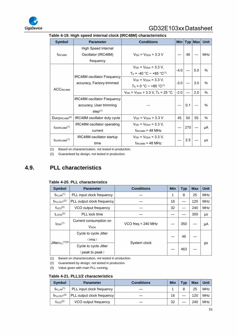
GD32E103xx Datasheet
55
Table 4-19. High speed internal clock (IRC48M) characteristics
Symbol Parameter Conditions Min Typ Max Unit
fIRC48M
High Speed Internal
Oscillator (IRC48M)
frequency
VDD = VDDA = 3.3 V — 48 — MHz
ACCIRC48M
IRC48M oscillator Frequency
accuracy, Factory-trimmed
VDD = VDDA = 3.3 V,
TA = -40 °C ~ +85 °C(1) -4.0 — 5.0 %
VDD = VDDA = 3.3 V,
TA = 0 °C ~ +85 °C(1) -3.0 — 3.0 %
VDD = VDDA = 3.3 V, TA = 25 °C -2.0 — 2.0 %
IRC48M oscillator Frequency
accuracy, User trimming
step(1)
— — 0.1 — %
DucyIRC48M(2) IRC48M oscillator duty cycle VDD = VDDA = 3.3 V 45 50 55 %
IDDIRC48M(1)
IRC48M oscillator operating
current
VDD = VDDA = 3.3 V,
fIRC48M = 48 MHz — 270 — μA
tSUIRC48M(1)
IRC48M oscillator startup
time
VDD = VDDA = 3.3 V,
fIRC48M = 48 MHz — 2.5 — μs
(1) Based on characterization, not tested in production.
(2) Guaranteed by design, not tested in production.
4.9. PLL characteristics
Table 4-20. PLL characteristics
Symbol Parameter Conditions Min Typ Max Unit
fPLLIN(1) PLL input clock frequency — 1 8 25 MHz
fPLLOUT(2) PLL output clock frequency — 16 — 120 MHz
fVCO(2) VCO output frequency — 32 — 240 MHz
tLOCK(2) PLL lock time — — — 300 μs
IDDA(1)
Current consumption on
VDDA VCO freq = 240 MHz — 350 — μA
JitterPLL(1)(3)
Cycle to cycle Jitter
(rms) System clock
— 46 —
ps Cycle to cycle Jitter
(peak to peak) — 463 —
(1) Based on characterization, not tested in production.
(2) Guaranteed by design, not tested in production.
(3) Value given with main PLL running.
Table 4-21. PLL1/2 characteristics
Symbol Parameter Conditions Min Typ Max Unit
fPLLIN(1) PLL input clock frequency — 1 8 25 MHz
fPLLOUT(2) PLL output clock frequency — 16 — 120 MHz
fVCO(2) VCO output frequency — 32 — 240 MHz
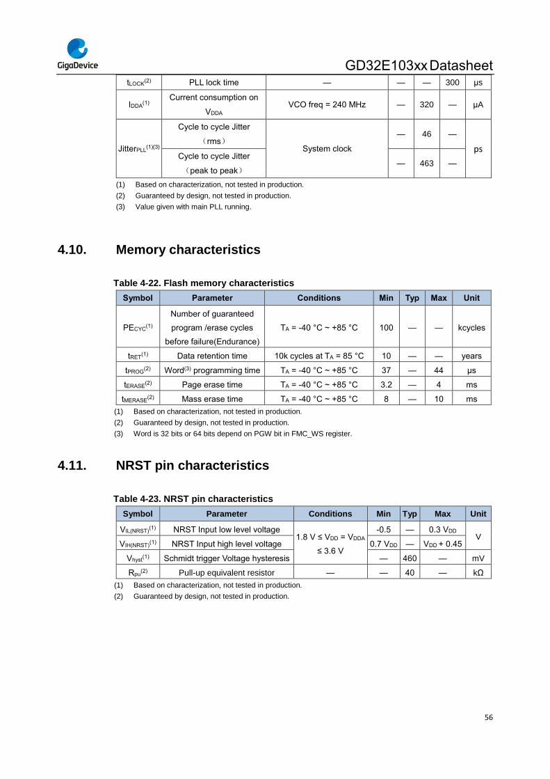
GD32E103xx Datasheet
56
tLOCK(2) PLL lock time — — — 300 μs
IDDA(1)
Current consumption on
VDDA VCO freq = 240 MHz — 320 — μA
JitterPLL(1)(3)
Cycle to cycle Jitter
(rms) System clock
— 46 —
ps Cycle to cycle Jitter
(peak to peak) — 463 —
(1) Based on characterization, not tested in production.
(2) Guaranteed by design, not tested in production.
(3) Value given with main PLL running.
4.10. Memory characteristics
Table 4-22. Flash memory characteristics
Symbol Parameter Conditions Min Typ Max Unit
PECYC(1)
Number of guaranteed
program /erase cycles
before failure(Endurance)
TA = -40 °C ~ +85 °C 100 — — kcycles
tRET(1) Data retention time 10k cycles at TA = 85 °C 10 — — years
tPROG(2) Word(3) programming time TA = -40 °C ~ +85 °C 37 — 44 μs
tERASE(2) Page erase time TA = -40 °C ~ +85 °C 3.2 — 4 ms
tMERASE(2) Mass erase time TA = -40 °C ~ +85 °C 8 — 10 ms
(1) Based on characterization, not tested in production.
(2) Guaranteed by design, not tested in production.
(3) Word is 32 bits or 64 bits depend on PGW bit in FMC_WS register.
4.11. NRST pin characteristics
Table 4-23. NRST pin characteristics
Symbol Parameter Conditions Min Typ Max Unit
VIL(NRST)(1) NRST Input low level voltage
1.8 V ≤ VDD = VDDA
≤ 3.6 V
-0.5 — 0.3 VDD V
VIH(NRST)(1) NRST Input high level voltage 0.7 VDD — VDD + 0.45
Vhyst(1) Schmidt trigger Voltage hysteresis — 460 — mV
Rpu(2) Pull-up equivalent resistor — — 40 — kΩ
(1) Based on characterization, not tested in production.
(2) Guaranteed by design, not tested in production.
GD32E103xx Datasheet
57
Figure 4-4. Recommended external NRST pin circuit
NRST
VDD
External reset circuit RPU10 kΩ
VDD
GND
100 nFK
4.12. GPIO characteristics
Table 4-24. I/O port DC characteristics(1)(3)
Symbol Parameter Conditions Min Typ Max Unit
VIL
Standard IO Low level input voltage 1.8 V ≤ VDD = VDDA ≤ 3.6
V — — 0.3 VDD V
5V-tolerant IO Low level input voltage 1.8 V ≤ VDD = VDDA ≤ 3.6
V — — 0.3 VDD V
VIH
Standard IO High level input voltage 1.8 V ≤ VDD = VDDA ≤ 3.6
V
0.7
VDD — — V
5V-tolerant IO High level input voltage 1.8 V ≤ VDD = VDDA ≤ 3.6
V
0.7
VDD — — V
VOL Low level output voltage
(IIO = +8 mA)
VDD = 1.8 V — — 0.32
V VDD = 2.5 V — — 0.24
VDD = 3.3 V — — 0.11
VDD = 3.6 V — — 0.11
VOL Low level output voltage
(IIO = +20 mA)
VDD = 1.8 V — — 0.53
V VDD = 2.5 V — — 0.60
VDD = 3.3 V — — 0.28
VDD = 3.6 V — — 0.27
VOH High level output voltage
(IIO = +8 mA)
VDD = 1.8 V 1.49 — —
V VDD = 2.5 V 2.27 — —
VDD = 3.3 V 3.14 — —
VDD = 3.6 V 3.45 — —
VOH High level output voltage
(IIO = +20 mA)
VDD = 1.8 V 1.25 — —
V VDD = 2.5 V 1.89 — —
VDD = 3.3 V 2.91 — —
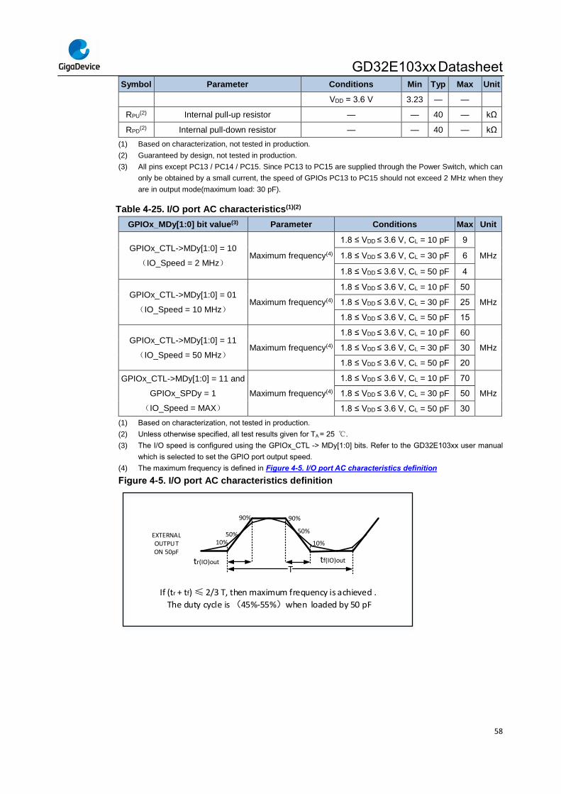
GD32E103xx Datasheet
58
Symbol Parameter Conditions Min Typ Max Unit
VDD = 3.6 V 3.23 — —
RPU(2) Internal pull-up resistor — — 40 — kΩ
RPD(2) Internal pull-down resistor — — 40 — kΩ
(1) Based on characterization, not tested in production.
(2) Guaranteed by design, not tested in production.
(3) All pins except PC13 / PC14 / PC15. Since PC13 to PC15 are supplied through the Power Switch, which can
only be obtained by a small current, the speed of GPIOs PC13 to PC15 should not exceed 2 MHz when they
are in output mode(maximum load: 30 pF).
Table 4-25. I/O port AC characteristics(1)(2)
GPIOx_MDy[1:0] bit value(3) Parameter Conditions Max Unit
GPIOx_CTL->MDy[1:0] = 10
(IO_Speed = 2 MHz) Maximum frequency(4)
1.8 ≤ VDD ≤ 3.6 V, CL = 10 pF 9
MHz 1.8 ≤ VDD ≤ 3.6 V, CL = 30 pF 6
1.8 ≤ VDD ≤ 3.6 V, CL = 50 pF 4
GPIOx_CTL->MDy[1:0] = 01
(IO_Speed = 10 MHz) Maximum frequency(4)
1.8 ≤ VDD ≤ 3.6 V, CL = 10 pF 50
MHz 1.8 ≤ VDD ≤ 3.6 V, CL = 30 pF 25
1.8 ≤ VDD ≤ 3.6 V, CL = 50 pF 15
GPIOx_CTL->MDy[1:0] = 11
(IO_Speed = 50 MHz) Maximum frequency(4)
1.8 ≤ VDD ≤ 3.6 V, CL = 10 pF 60
MHz 1.8 ≤ VDD ≤ 3.6 V, CL = 30 pF 30
1.8 ≤ VDD ≤ 3.6 V, CL = 50 pF 20
GPIOx_CTL->MDy[1:0] = 11 and
GPIOx_SPDy = 1
(IO_Speed = MAX)
Maximum frequency(4)
1.8 ≤ VDD ≤ 3.6 V, CL = 10 pF 70
MHz 1.8 ≤ VDD ≤ 3.6 V, CL = 30 pF 50
1.8 ≤ VDD ≤ 3.6 V, CL = 50 pF 30
(1) Based on characterization, not tested in production.
(2) Unless otherwise specified, all test results given for TA = 25 ℃.
(3) The I/O speed is configured using the GPIOx_CTL -> MDy[1:0] bits. Refer to the GD32E103xx user manual
which is selected to set the GPIO port output speed.
(4) The maximum frequency is defined in Figure 4-5. I/O port AC characteristics definition
Figure 4-5. I/O port AC characteristics definition
T
10%50%
90%
10%
90%
50%
tr(IO)out tf(IO)out
EXTERNALOUTPUTON 50pF
If (tr + tf) ≤ 2/3 T, then maximum frequency is achieved .
The duty cycle is (45%-55%)when loaded by 50 pF
GD32E103xx Datasheet
59
4.13. ADC characteristics
Table 4-26. ADC characteristics
Symbol Parameter Conditions Min Typ Max Unit
VDDA(1) Operating voltage — 2.4 3.3 3.6 V
VIN(1) ADC input voltage range — 0 — VREF+ V
fADC(1) ADC clock — 0.1 — 42 MHz
fS(1) Sampling rate
12-bit 0.007 — 3
MSPS 10-bit 0.008 — 3.5
8-bit 0.01 — 4.2
6-bit 0.011 — 5.25
VAIN(1) Analog input voltage 16 external; 2 internal 0 — VDDA V
VREF+(2) Positive Reference Voltage — 1.8 — VDDA V
VREF-(2)
Negative Reference
Voltage — — VSSA — V
RAIN(2) External input impedance See Equation 1 — — 24 kΩ
RADC(2)
Input sampling switch
resistance — — — 0.2 kΩ
CADC(2) Input sampling capacitance
No pin/pad capacitance
included — — 5.5 pF
tCAL(2) Calibration time fADC = 42 MHz — 3.12 — μs
ts(2) Sampling time fADC = 42 MHz 0.036 — 5.7 μs
tCONV(2)
Total conversion
time(including sampling
time)
12-bit — 14 —
1/ fADC 10-bit — 12 —
8-bit — 10 —
6-bit — 8 —
tSU(2) Startup time — — — 1 μs
(1) Based on characterization, not tested in production.
(2) Guaranteed by design, not tested in production.
Equation 1: RAIN max formula RAIN <Ts
fADC∗CADC∗ln (2N+2)− RADC
The formula above (Equation 1) is used to determine the maximum external impedance allowed for an
error below 1/4 of LSB. Here N = 12 (from 12-bit resolution).
Table 4-27. ADC RAIN max for fADC = 42 MHz
Ts(cycles) ts(us) RAINmax (kΩ)
1.5 0.04 0.47
7.5 0.18 3.15
13.5 0.32 5.82
28.5 0.68 12.55
41.5 0.99 18.35
55.5 1.32 24.55
71.5 1.70 NA
GD32E103xx Datasheet
60
Ts(cycles) ts(us) RAINmax (kΩ)
239.5 5.70 NA
Table 4-28. ADC dynamic accuracy at fADC = 14 MHz(1)
Symbol Parameter Test conditions Min Typ Max Unit
ENOB Effective number of bits fADC = 14 MHz
VDDA = VREF+ = 3.3 V
Input Frequency = 20
kHz
Temperature = 25 ℃
— 10.3 — bits
SNDR Signal-to-noise and distortion ratio — 63.8 —
dB SNR Signal-to-noise ratio — 64.5 —
THD Total harmonic distortion — -67.5 —
(1) Based on characterization, not tested in production.
Table 4-29. ADC dynamic accuracy at fADC = 42 MHz(1)
Symbol Parameter Test conditions Min Typ Max Unit
ENOB Effective number of bits fADC = 42 MHz
VDDA = VREF+ = 3.3 V
Input Frequency = 20 kHz
Temperature = 25 ℃
— 10.3 — bits
SNDR Signal-to-noise and distortion ratio — 63.8 —
dB SNR Signal-to-noise ratio — 64.5 —
THD Total harmonic distortion — -67.5 —
(1) Based on characterization, not tested in production.
Table 4-30. ADC static accuracy at fADC = 42 MHz(1)
Symbol Parameter Test conditions Typ Max Unit
Offset Offset error fADC = 42 MHz
VDDA = VREF+ = 3.3 V
±1 —
LSB DNL Differential linearity error ±1 —
INL Integral linearity error ±3 —
(1) Based on characterization, not tested in production.
4.14. Temperature sensor characteristics
Table 4-31. Temperature sensor characteristics(1)
Symbol Parameter Min Typ Max Unit
TL VSENSE linearity with temperature — ±1.5 — ℃
Avg_Slope Average slope — 4.3 — mV/℃
V25 Voltage at 25 °C — 1.47 — V
tSTART Startup time — — — μs
tS_temp(2) ADC sampling time when reading the temperature — 17.1 — μs
(1) Based on characterization, not tested in production.
(2) Shortest sampling time can be determined in the application by multiple iterations.
4.15. DAC characteristics
Table 4-32. DAC characteristics
GD32E103xx Datasheet
61
Symbol Parameter Conditions Min Typ Max Unit
VDDA(1) Operating voltage — 1.71 3.3 3.6 V
VREF+(1) Reference supply voltage — 1.8 — VDDA V
VREF-(1)
Negative Reference
Voltage — — VSSA — V
RLOAD(2) Load resistance
Resistive load with
buffer ON 5 — — kΩ
Ro(2) Impedance output with
buffer OFF — — — 15 kΩ
CLOAD(2) Load capacitance
No pin/pad capacitance
included — — 50 pF
DAC_OUT
min(2)
Lower DAC_OUT voltage
with buffer ON — 0.2 — — V
DAC_OUT
max(2)
Higher DAC_OUT voltage
with buffer ON — — —
VDDA-
0.2 V
DAC_OUT
min(2)
Lower DAC_OUT voltage
with buffer OFF — — 0.5 — mV
DAC_OUT
max(2)
Higher DAC_OUT voltage
with buffer OFF — — —
VDDA-
1LSB V
IDDA(1)
DAC current consumption
in quiescent mode
With no load, middle
code(0x800) on the input, VREF+
= 3.6 V
— 380 — μA
With no load, worst
code(0xF1C) on the input, VREF+
= 3.6 V
— 460 — μA
IDDVREF+(1)
DAC current consumption
in quiescent mode
With no load, middle
code(0x800) on the input, VREF+
= 3.6 V
— 120 — μA
With no load, worst
code(0xF1C) on the input, VREF+
= 3.6 V
— 320 — μA
DNL(1) Differential non-linearity
error DAC in 12-bit mode — — ±3 LSB
INL(1) Integral non-linearity DAC in 12-bit mode — — ±4 LSB
Offset(1) Offset error DAC in 12-bit mode — — ±12 LSB
GE(1) Gain error DAC in 12-bit mode — — ±0.5 %
Tsetting(1) Settling time CLOAD ≤ 50 pF, RLOAD ≥ 5 kΩ — 0.3 1 μs
Twakeup(2) Wakeup from off state — — 5 10 μs
Update
rate(2)
Max frequency for a correct
DAC_OUT change from
code i to i±1LSBs
CLOAD ≤ 50 pF, RLOAD ≥ 5 kΩ — — 4 MS/s
PSRR(2) Power supply rejection
ratio — 55 80 — dB
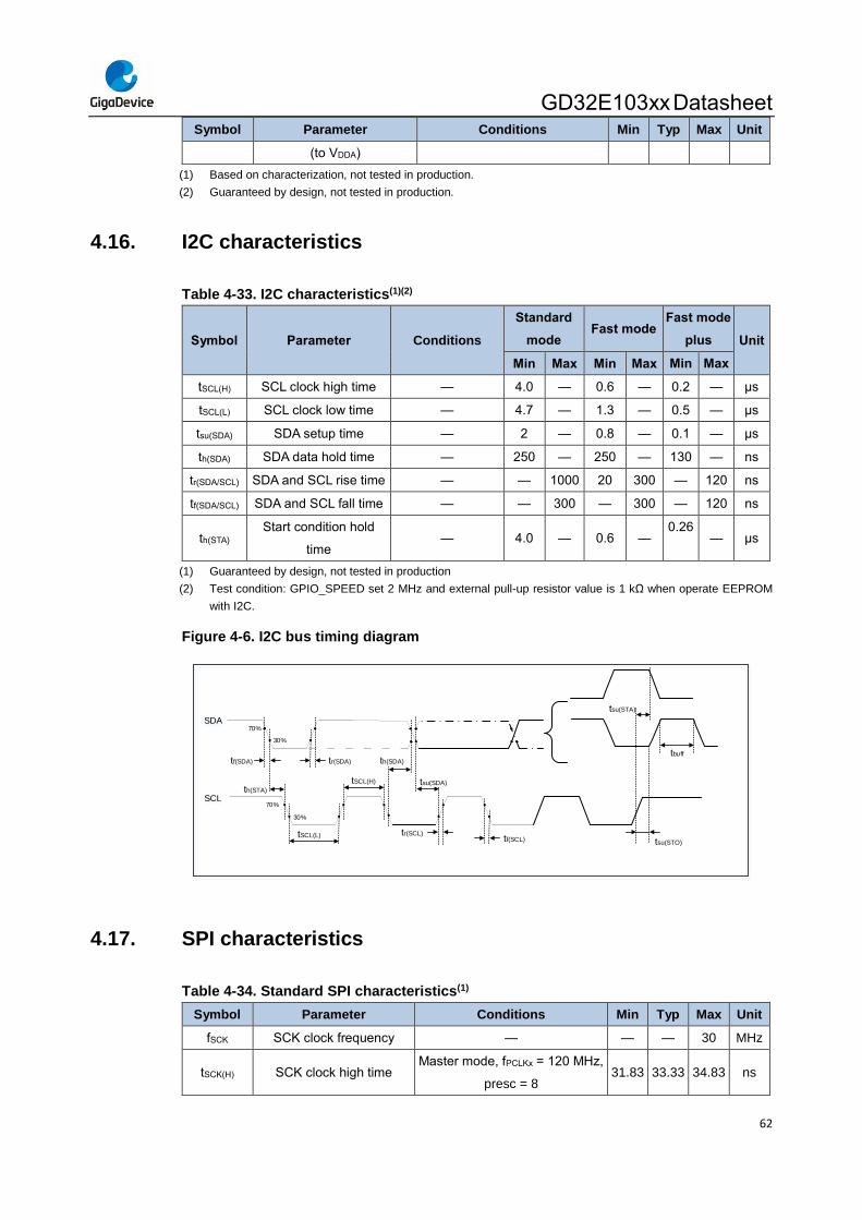
GD32E103xx Datasheet
62
Symbol Parameter Conditions Min Typ Max Unit
(to VDDA)
(1) Based on characterization, not tested in production.
(2) Guaranteed by design, not tested in production.
4.16. I2C characteristics
Table 4-33. I2C characteristics(1)(2)
Symbol Parameter Conditions
Standard
mode Fast mode
Fast mode
plus Unit
Min Max Min Max Min Max
tSCL(H) SCL clock high time — 4.0 — 0.6 — 0.2 — μs
tSCL(L) SCL clock low time — 4.7 — 1.3 — 0.5 — μs
tsu(SDA) SDA setup time — 2 — 0.8 — 0.1 — μs
th(SDA) SDA data hold time — 250 — 250 — 130 — ns
tr(SDA/SCL) SDA and SCL rise time — — 1000 20 300 — 120 ns
tf(SDA/SCL) SDA and SCL fall time — — 300 — 300 — 120 ns
th(STA) Start condition hold
time — 4.0 — 0.6 —
0.26 — μs
(1) Guaranteed by design, not tested in production
(2) Test condition: GPIO_SPEED set 2 MHz and external pull-up resistor value is 1 kΩ when operate EEPROM
with I2C.
Figure 4-6. I2C bus timing diagram
70%
30%
tf(SDA)
30%
70%
tr(SDA)
th(STA)
tSCL(L)
tSCL(H)
tr(SCL)tf(SCL)
th(SDA)
tsu(SDA)
SDA
SCL
tbuff
tsu(STA)
tsu(STO)
4.17. SPI characteristics
Table 4-34. Standard SPI characteristics(1)
Symbol Parameter Conditions Min Typ Max Unit
fSCK SCK clock frequency — — — 30 MHz
tSCK(H) SCK clock high time Master mode, fPCLKx = 120 MHz,
presc = 8 31.83 33.33 34.83 ns
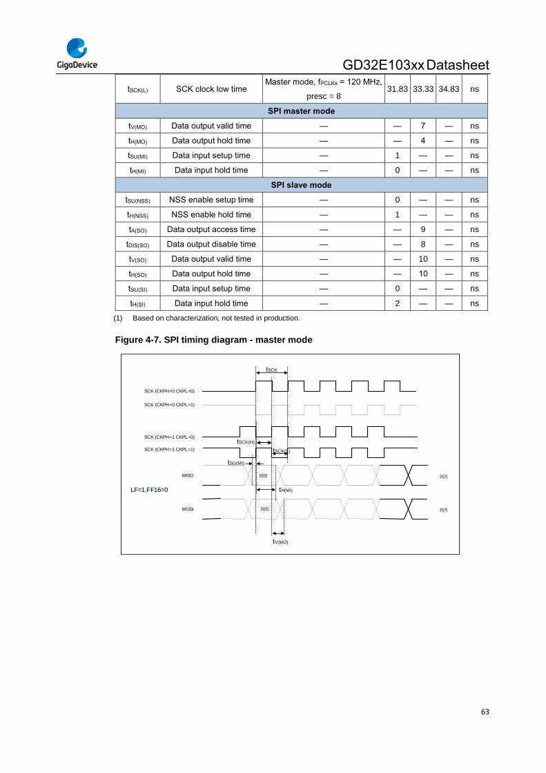
GD32E103xx Datasheet
63
tSCK(L) SCK clock low time Master mode, fPCLKx = 120 MHz,
presc = 8 31.83 33.33 34.83 ns
SPI master mode
tV(MO) Data output valid time — — 7 — ns
tH(MO) Data output hold time — — 4 — ns
tSU(MI) Data input setup time — 1 — — ns
tH(MI) Data input hold time — 0 — — ns
SPI slave mode
tSU(NSS) NSS enable setup time — 0 — — ns
tH(NSS) NSS enable hold time — 1 — — ns
tA(SO) Data output access time — — 9 — ns
tDIS(SO) Data output disable time — — 8 — ns
tV(SO) Data output valid time — — 10 — ns
tH(SO) Data output hold time — — 10 — ns
tSU(SI) Data input setup time — 0 — — ns
tH(SI) Data input hold time — 2 — — ns
(1) Based on characterization, not tested in production.
Figure 4-7. SPI timing diagram - master mode
SCK (CKPH=0 CKPL=0)
SCK (CKPH=0 CKPL=1)
SCK (CKPH=1 CKPL=0)
SCK (CKPH=1 CKPL=1)
MISO
MOSI
D[0]
LF=1,FF16=0
D[0]
D[7]
D[7]
tSCK
tSCK(H)
tSCK(L)
tH(MI)
tSU(MI)
tV(MO)
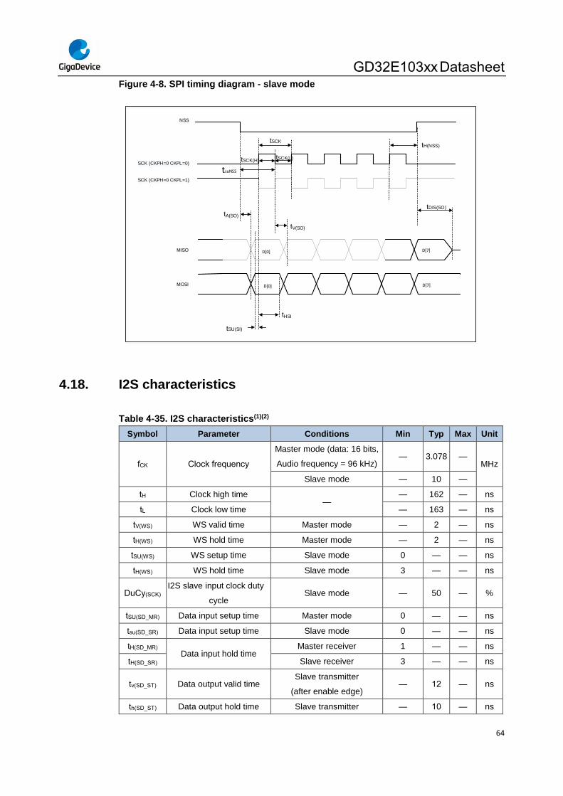
GD32E103xx Datasheet
64
Figure 4-8. SPI timing diagram - slave mode
SCK (CKPH=0 CKPL=0)
SCK (CKPH=0 CKPL=1)
MISO
MOSI
D[0]
D[0]
D[7]
D[7]
tA(SO)
tsuNSS
NSS
tV(SO)
tHSI
tSU(SI)
tDIS(SO)
tH(NSS)tSCK
tSCK(H)tSCK(L)
4.18. I2S characteristics
Table 4-35. I2S characteristics(1)(2)
Symbol Parameter Conditions Min Typ Max Unit
fCK Clock frequency
Master mode (data: 16 bits,
Audio frequency = 96 kHz) — 3.078 —
MHz
Slave mode — 10 —
tH Clock high time —
— 162 — ns
tL Clock low time — 163 — ns
tV(WS) WS valid time Master mode — 2 — ns
tH(WS) WS hold time Master mode — 2 — ns
tSU(WS) WS setup time Slave mode 0 — — ns
tH(WS) WS hold time Slave mode 3 — — ns
DuCy(SCK) I2S slave input clock duty
cycle Slave mode — 50 — %
tSU(SD_MR) Data input setup time Master mode 0 — — ns
tsu(SD_SR) Data input setup time Slave mode 0 — — ns
tH(SD_MR) Data input hold time
Master receiver 1 — — ns
tH(SD_SR) Slave receiver 3 — — ns
tv(SD_ST) Data output valid time Slave transmitter
(after enable edge) — 12 — ns
th(SD_ST) Data output hold time Slave transmitter — 10 — ns
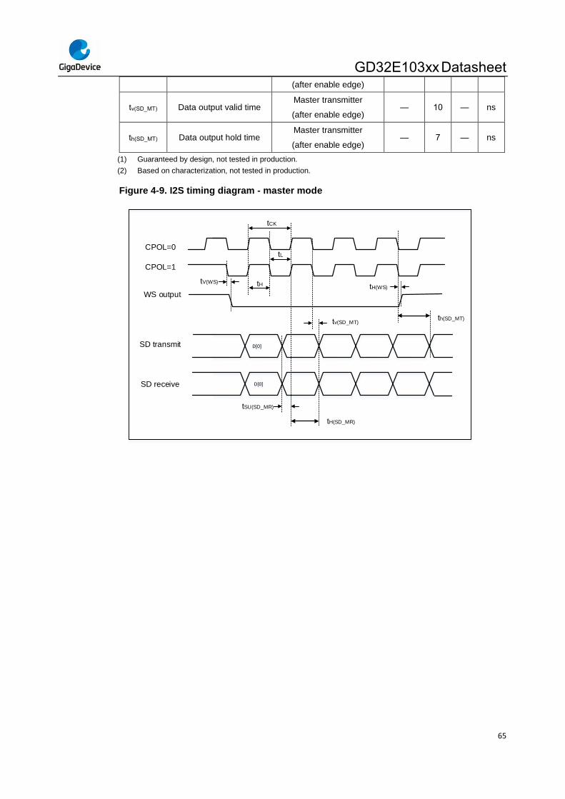
GD32E103xx Datasheet
65
(after enable edge)
tv(SD_MT) Data output valid time Master transmitter
(after enable edge) — 10 — ns
th(SD_MT) Data output hold time Master transmitter
(after enable edge) — 7 — ns
(1) Guaranteed by design, not tested in production.
(2) Based on characterization, not tested in production.
Figure 4-9. I2S timing diagram - master mode
tCK
D[0]
D[0]
tH
tL
tSU(SD_MR)
tH(SD_MR)
tv(SD_MT)th(SD_MT)
CPOL=0
CPOL=1
WS output
SD transmit
SD receive
tV(WS)tH(WS)
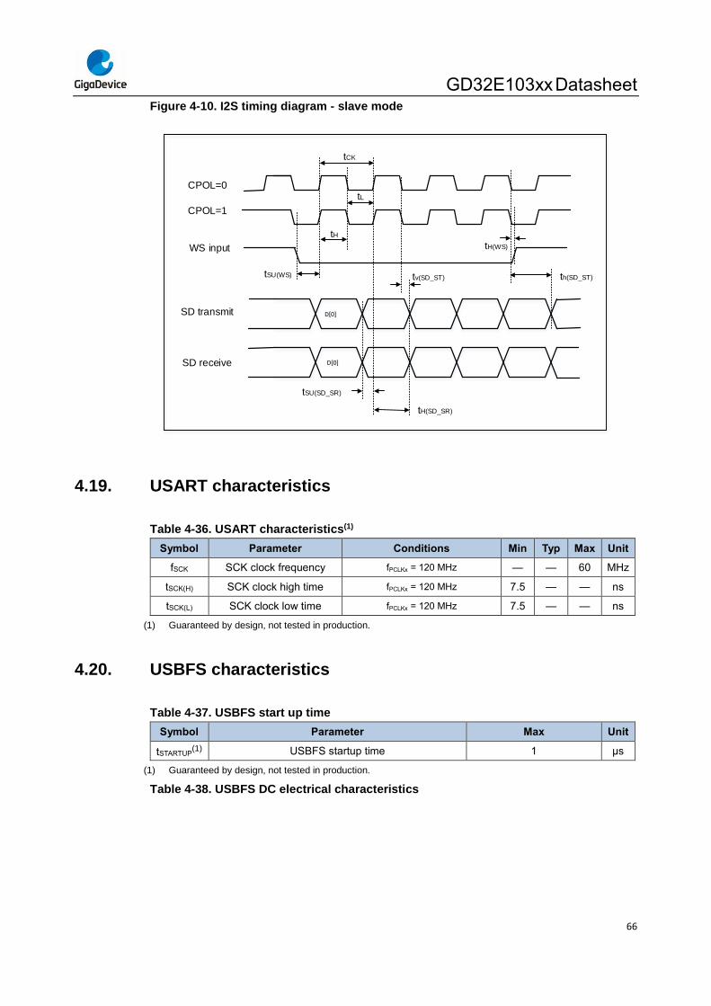
GD32E103xx Datasheet
66
Figure 4-10. I2S timing diagram - slave mode
tCK
D[0]
D[0]
tH
tL
tSU(SD_SR)
tH(SD_SR)
tv(SD_ST) th(SD_ST)
CPOL=0
CPOL=1
WS input
SD transmit
SD receive
tH(WS)
tSU(WS)
4.19. USART characteristics
Table 4-36. USART characteristics(1)
Symbol Parameter Conditions Min Typ Max Unit
fSCK SCK clock frequency fPCLKx = 120 MHz — — 60 MHz
tSCK(H) SCK clock high time fPCLKx = 120 MHz 7.5 — — ns
tSCK(L) SCK clock low time fPCLKx = 120 MHz 7.5 — — ns
(1) Guaranteed by design, not tested in production.
4.20. USBFS characteristics
Table 4-37. USBFS start up time
Symbol Parameter Max Unit
tSTARTUP(1) USBFS startup time 1 μs
(1) Guaranteed by design, not tested in production.
Table 4-38. USBFS DC electrical characteristics
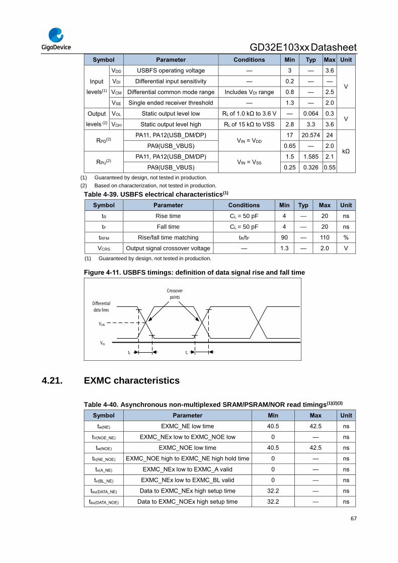
GD32E103xx Datasheet
67
Symbol Parameter Conditions Min Typ Max Unit
Input
levels(1)
VDD USBFS operating voltage — 3 — 3.6
V VDI
Differential input sensitivity — 0.2 — —
VCM Differential common mode range Includes VDI range 0.8 — 2.5
VSE Single ended receiver threshold — 1.3 — 2.0
Output
levels (2)
VOL Static output level low RL of 1.0 kΩ to 3.6 V — 0.064 0.3 V
VOH Static output level high RL of 15 kΩ to VSS 2.8 3.3 3.6
RPD(2)
PA11, PA12(USB_DM/DP) VIN = VDD
17 20.574 24
kΩ PA9(USB_VBUS) 0.65 — 2.0
RPU(2)
PA11, PA12(USB_DM/DP) VIN = VSS
1.5 1.585 2.1
PA9(USB_VBUS) 0.25 0.326 0.55
(1) Guaranteed by design, not tested in production.
(2) Based on characterization, not tested in production.
Table 4-39. USBFS electrical characteristics(1)
Symbol Parameter Conditions Min Typ Max Unit
tR Rise time CL = 50 pF 4 — 20 ns
tF Fall time CL = 50 pF 4 — 20 ns
tRFM Rise/fall time matching tR/tF 90 — 110 %
VCRS Output signal crossover voltage — 1.3 — 2.0 V
(1) Guaranteed by design, not tested in production.
Figure 4-11. USBFS timings: definition of data signal rise and fall time
tf tr
VSS
VCRS
Crossoverpoints
Differentialdata lines
4.21. EXMC characteristics
Table 4-40. Asynchronous non-multiplexed SRAM/PSRAM/NOR read timings(1)(2)(3)
Symbol Parameter Min Max Unit
tw(NE) EXMC_NE low time 40.5 42.5 ns
tV(NOE_NE) EXMC_NEx low to EXMC_NOE low 0 — ns
tw(NOE) EXMC_NOE low time 40.5 42.5 ns
th(NE_NOE) EXMC_NOE high to EXMC_NE high hold time 0 — ns
tv(A_NE) EXMC_NEx low to EXMC_A valid 0 — ns
tv(BL_NE) EXMC_NEx low to EXMC_BL valid 0 — ns
tsu(DATA_NE) Data to EXMC_NEx high setup time 32.2 — ns
tsu(DATA_NOE) Data to EXMC_NOEx high setup time 32.2 — ns
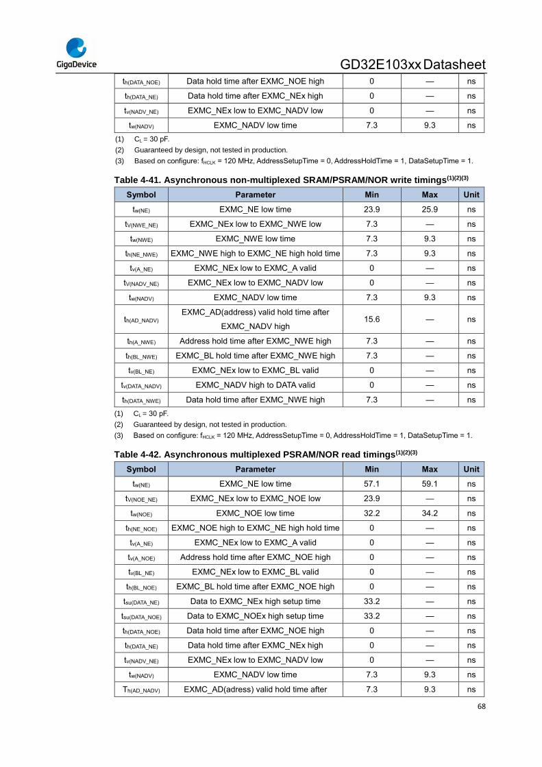
GD32E103xx Datasheet
68
th(DATA_NOE) Data hold time after EXMC_NOE high 0 — ns
th(DATA_NE) Data hold time after EXMC_NEx high 0 — ns
tv(NADV_NE) EXMC_NEx low to EXMC_NADV low 0 — ns
tw(NADV) EXMC_NADV low time 7.3 9.3 ns
(1) CL = 30 pF.
(2) Guaranteed by design, not tested in production.
(3) Based on configure: fHCLK = 120 MHz, AddressSetupTime = 0, AddressHoldTime = 1, DataSetupTime = 1.
Table 4-41. Asynchronous non-multiplexed SRAM/PSRAM/NOR write timings(1)(2)(3)
Symbol Parameter Min Max Unit
tw(NE) EXMC_NE low time 23.9 25.9 ns
tV(NWE_NE) EXMC_NEx low to EXMC_NWE low 7.3 — ns
tw(NWE) EXMC_NWE low time 7.3 9.3 ns
th(NE_NWE) EXMC_NWE high to EXMC_NE high hold time 7.3 9.3 ns
tv(A_NE) EXMC_NEx low to EXMC_A valid 0 — ns
tV(NADV_NE) EXMC_NEx low to EXMC_NADV low 0 — ns
tw(NADV) EXMC_NADV low time 7.3 9.3 ns
th(AD_NADV) EXMC_AD(address) valid hold time after
EXMC_NADV high 15.6 — ns
th(A_NWE) Address hold time after EXMC_NWE high 7.3 — ns
th(BL_NWE) EXMC_BL hold time after EXMC_NWE high 7.3 — ns
tv(BL_NE) EXMC_NEx low to EXMC_BL valid 0 — ns
tv(DATA_NADV) EXMC_NADV high to DATA valid 0 — ns
th(DATA_NWE) Data hold time after EXMC_NWE high 7.3 — ns
(1) CL = 30 pF.
(2) Guaranteed by design, not tested in production.
(3) Based on configure: fHCLK = 120 MHz, AddressSetupTime = 0, AddressHoldTime = 1, DataSetupTime = 1.
Table 4-42. Asynchronous multiplexed PSRAM/NOR read timings(1)(2)(3)
Symbol Parameter Min Max Unit
tw(NE) EXMC_NE low time 57.1 59.1 ns
tV(NOE_NE) EXMC_NEx low to EXMC_NOE low 23.9 — ns
tw(NOE) EXMC_NOE low time 32.2 34.2 ns
th(NE_NOE) EXMC_NOE high to EXMC_NE high hold time 0 — ns
tv(A_NE) EXMC_NEx low to EXMC_A valid 0 — ns
tv(A_NOE) Address hold time after EXMC_NOE high 0 — ns
tv(BL_NE) EXMC_NEx low to EXMC_BL valid 0 — ns
th(BL_NOE) EXMC_BL hold time after EXMC_NOE high 0 — ns
tsu(DATA_NE) Data to EXMC_NEx high setup time 33.2 — ns
tsu(DATA_NOE) Data to EXMC_NOEx high setup time 33.2 — ns
th(DATA_NOE) Data hold time after EXMC_NOE high 0 — ns
th(DATA_NE) Data hold time after EXMC_NEx high 0 — ns
tv(NADV_NE) EXMC_NEx low to EXMC_NADV low 0 — ns
tw(NADV) EXMC_NADV low time 7.3 9.3 ns
Th(AD_NADV) EXMC_AD(adress) valid hold time after 7.3 9.3 ns
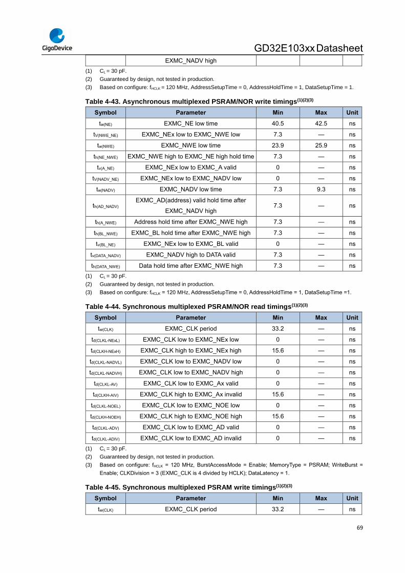
GD32E103xx Datasheet
69
EXMC_NADV high
(1) CL = 30 pF. (2) Guaranteed by design, not tested in production. (3) Based on configure: fHCLK = 120 MHz, AddressSetupTime = 0, AddressHoldTime = 1, DataSetupTime = 1.
Table 4-43. Asynchronous multiplexed PSRAM/NOR write timings(1)(2)(3)
Symbol Parameter Min Max Unit
tw(NE) EXMC_NE low time 40.5 42.5 ns
tV(NWE_NE) EXMC_NEx low to EXMC_NWE low 7.3 — ns
tw(NWE) EXMC_NWE low time 23.9 25.9 ns
th(NE_NWE) EXMC_NWE high to EXMC_NE high hold time 7.3 — ns
tv(A_NE) EXMC_NEx low to EXMC_A valid 0 — ns
tV(NADV_NE) EXMC_NEx low to EXMC_NADV low 0 — ns
tw(NADV) EXMC_NADV low time 7.3 9.3 ns
th(AD_NADV) EXMC_AD(address) valid hold time after
EXMC_NADV high 7.3 — ns
th(A_NWE) Address hold time after EXMC_NWE high 7.3 — ns
th(BL_NWE) EXMC_BL hold time after EXMC_NWE high 7.3 — ns
tv(BL_NE) EXMC_NEx low to EXMC_BL valid 0 — ns
tv(DATA_NADV) EXMC_NADV high to DATA valid 7.3 — ns
th(DATA_NWE) Data hold time after EXMC_NWE high 7.3 — ns
(1) CL = 30 pF. (2) Guaranteed by design, not tested in production. (3) Based on configure: fHCLK = 120 MHz, AddressSetupTime = 0, AddressHoldTime = 1, DataSetupTime =1.
Table 4-44. Synchronous multiplexed PSRAM/NOR read timings(1)(2)(3)
Symbol Parameter Min Max Unit
tw(CLK) EXMC_CLK period 33.2 — ns
td(CLKL-NExL) EXMC_CLK low to EXMC_NEx low 0 — ns
td(CLKH-NExH) EXMC_CLK high to EXMC_NEx high 15.6 — ns
td(CLKL-NADVL) EXMC_CLK low to EXMC_NADV low 0 — ns
td(CLKL-NADVH) EXMC_CLK low to EXMC_NADV high 0 — ns
td(CLKL-AV) EXMC_CLK low to EXMC_Ax valid 0 — ns
td(CLKH-AIV) EXMC_CLK high to EXMC_Ax invalid 15.6 — ns
td(CLKL-NOEL) EXMC_CLK low to EXMC_NOE low 0 — ns
td(CLKH-NOEH) EXMC_CLK high to EXMC_NOE high 15.6 — ns
td(CLKL-ADV) EXMC_CLK low to EXMC_AD valid 0 — ns
td(CLKL-ADIV) EXMC_CLK low to EXMC_AD invalid 0 — ns
(1) CL = 30 pF. (2) Guaranteed by design, not tested in production. (3) Based on configure: fHCLK = 120 MHz, BurstAccessMode = Enable; MemoryType = PSRAM; WriteBurst =
Enable; CLKDivision = 3 (EXMC_CLK is 4 divided by HCLK); DataLatency = 1.
Table 4-45. Synchronous multiplexed PSRAM write timings(1)(2)(3)
Symbol Parameter Min Max Unit
tw(CLK) EXMC_CLK period 33.2 — ns
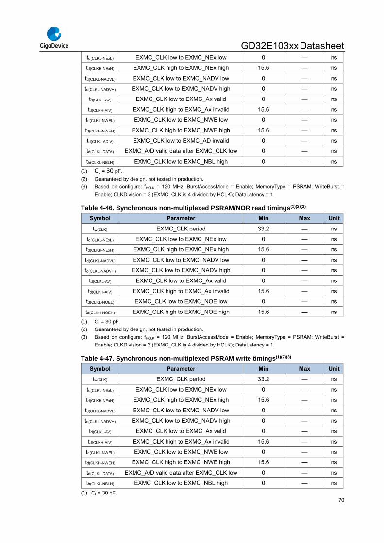
GD32E103xx Datasheet
70
td(CLKL-NExL) EXMC_CLK low to EXMC_NEx low 0 — ns
td(CLKH-NExH) EXMC_CLK high to EXMC_NEx high 15.6 — ns
td(CLKL-NADVL) EXMC_CLK low to EXMC_NADV low 0 — ns
td(CLKL-NADVH) EXMC_CLK low to EXMC_NADV high 0 — ns
td(CLKL-AV) EXMC_CLK low to EXMC_Ax valid 0 — ns
td(CLKH-AIV) EXMC_CLK high to EXMC_Ax invalid 15.6 — ns
td(CLKL-NWEL) EXMC_CLK low to EXMC_NWE low 0 — ns
td(CLKH-NWEH) EXMC_CLK high to EXMC_NWE high 15.6 — ns
td(CLKL-ADIV) EXMC_CLK low to EXMC_AD invalid 0 — ns
td(CLKL-DATA) EXMC_A/D valid data after EXMC_CLK low 0 — ns
th(CLKL-NBLH) EXMC_CLK low to EXMC_NBL high 0 — ns
(1) CL = 30 pF. (2) Guaranteed by design, not tested in production. (3) Based on configure: fHCLK = 120 MHz, BurstAccessMode = Enable; MemoryType = PSRAM; WriteBurst =
Enable; CLKDivision = 3 (EXMC_CLK is 4 divided by HCLK); DataLatency = 1.
Table 4-46. Synchronous non-multiplexed PSRAM/NOR read timings(1)(2)(3)
Symbol Parameter Min Max Unit
tw(CLK) EXMC_CLK period 33.2 — ns
td(CLKL-NExL) EXMC_CLK low to EXMC_NEx low 0 — ns
td(CLKH-NExH) EXMC_CLK high to EXMC_NEx high 15.6 — ns
td(CLKL-NADVL) EXMC_CLK low to EXMC_NADV low 0 — ns
td(CLKL-NADVH) EXMC_CLK low to EXMC_NADV high 0 — ns
td(CLKL-AV) EXMC_CLK low to EXMC_Ax valid 0 — ns
td(CLKH-AIV) EXMC_CLK high to EXMC_Ax invalid 15.6 — ns
td(CLKL-NOEL) EXMC_CLK low to EXMC_NOE low 0 — ns
td(CLKH-NOEH) EXMC_CLK high to EXMC_NOE high 15.6 — ns
(1) CL = 30 pF.
(2) Guaranteed by design, not tested in production.
(3) Based on configure: fHCLK = 120 MHz, BurstAccessMode = Enable; MemoryType = PSRAM; WriteBurst =
Enable; CLKDivision = 3 (EXMC_CLK is 4 divided by HCLK); DataLatency = 1.
Table 4-47. Synchronous non-multiplexed PSRAM write timings(1)(2)(3)
Symbol Parameter Min Max Unit
tw(CLK) EXMC_CLK period 33.2 — ns
td(CLKL-NExL) EXMC_CLK low to EXMC_NEx low 0 — ns
td(CLKH-NExH) EXMC_CLK high to EXMC_NEx high 15.6 — ns
td(CLKL-NADVL) EXMC_CLK low to EXMC_NADV low 0 — ns
td(CLKL-NADVH) EXMC_CLK low to EXMC_NADV high 0 — ns
td(CLKL-AV) EXMC_CLK low to EXMC_Ax valid 0 — ns
td(CLKH-AIV) EXMC_CLK high to EXMC_Ax invalid 15.6 — ns
td(CLKL-NWEL) EXMC_CLK low to EXMC_NWE low 0 — ns
td(CLKH-NWEH) EXMC_CLK high to EXMC_NWE high 15.6 — ns
td(CLKL-DATA) EXMC_A/D valid data after EXMC_CLK low 0 — ns
th(CLKL-NBLH) EXMC_CLK low to EXMC_NBL high 0 — ns
(1) CL = 30 pF.
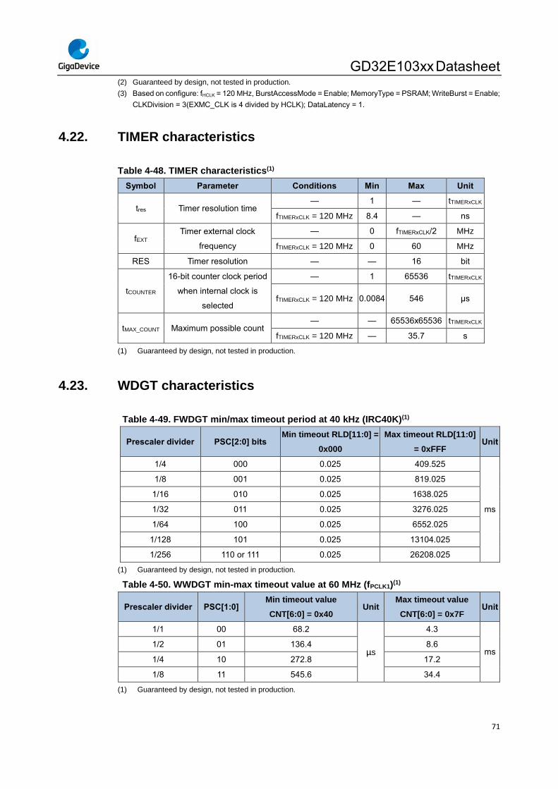
GD32E103xx Datasheet
71
(2) Guaranteed by design, not tested in production. (3) Based on configure: fHCLK = 120 MHz, BurstAccessMode = Enable; MemoryType = PSRAM; WriteBurst = Enable;
CLKDivision = 3(EXMC_CLK is 4 divided by HCLK); DataLatency = 1.
4.22. TIMER characteristics
Table 4-48. TIMER characteristics(1)
Symbol Parameter Conditions Min Max Unit
tres Timer resolution time — 1 — tTIMERxCLK
fTIMERxCLK = 120 MHz 8.4 — ns
fEXT Timer external clock
frequency
— 0 fTIMERxCLK/2 MHz
fTIMERxCLK = 120 MHz 0 60 MHz
RES Timer resolution — — 16 bit
tCOUNTER
16-bit counter clock period
when internal clock is
selected
— 1 65536 tTIMERxCLK
fTIMERxCLK = 120 MHz 0.0084 546 μs
tMAX_COUNT Maximum possible count — — 65536x65536 tTIMERxCLK
fTIMERxCLK = 120 MHz — 35.7 s
(1) Guaranteed by design, not tested in production.
4.23. WDGT characteristics
Table 4-49. FWDGT min/max timeout period at 40 kHz (IRC40K)(1)
Prescaler divider PSC[2:0] bits Min timeout RLD[11:0] =
0x000
Max timeout RLD[11:0]
= 0xFFF Unit
1/4 000 0.025 409.525
ms
1/8 001 0.025 819.025
1/16 010 0.025 1638.025
1/32 011 0.025 3276.025
1/64 100 0.025 6552.025
1/128 101 0.025 13104.025
1/256 110 or 111 0.025 26208.025
(1) Guaranteed by design, not tested in production.
Table 4-50. WWDGT min-max timeout value at 60 MHz (fPCLK1)(1)
Prescaler divider PSC[1:0] Min timeout value
CNT[6:0] = 0x40 Unit
Max timeout value
CNT[6:0] = 0x7F Unit
1/1 00 68.2
μs
4.3
ms 1/2 01 136.4 8.6
1/4 10 272.8 17.2
1/8 11 545.6 34.4
(1) Guaranteed by design, not tested in production.
GD32E103xx Datasheet
72
4.24. Parameter conditions
Unless otherwise specified, all values given for VDD = VDDA = 3.3 V, TA = 25 ℃.
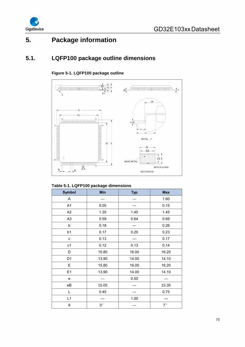
GD32E103xx Datasheet
73
5. Package information
5.1. LQFP100 package outline dimensions
Figure 5-1. LQFP100 package outline
AA2
A1
A3
F
B
E1 E
D
D1
eb
125
50
5175
76
100 26
B
cθ
0.25
L
L1
DETAIL: F
eB
BASE METAL
WITH PLATING
SECTION B-B
b
b1
c1 c
Table 5-1. LQFP100 package dimensions
Symbol Min Typ Max
A — — 1.60
A1 0.05 — 0.15
A2 1.35 1.40 1.45
A3 0.59 0.64 0.69
b 0.18 — 0.26
b1 0.17 0.20 0.23
c 0.13 — 0.17
c1 0.12 0.13 0.14
D 15.80 16.00 16.20
D1 13.90 14.00 14.10
E 15.80 16.00 16.20
E1 13.90 14.00 14.10
e — 0.50 —
eB 15.05 — 15.35
L 0.45 — 0.75
L1 — 1.00 —
θ 0° — 7°
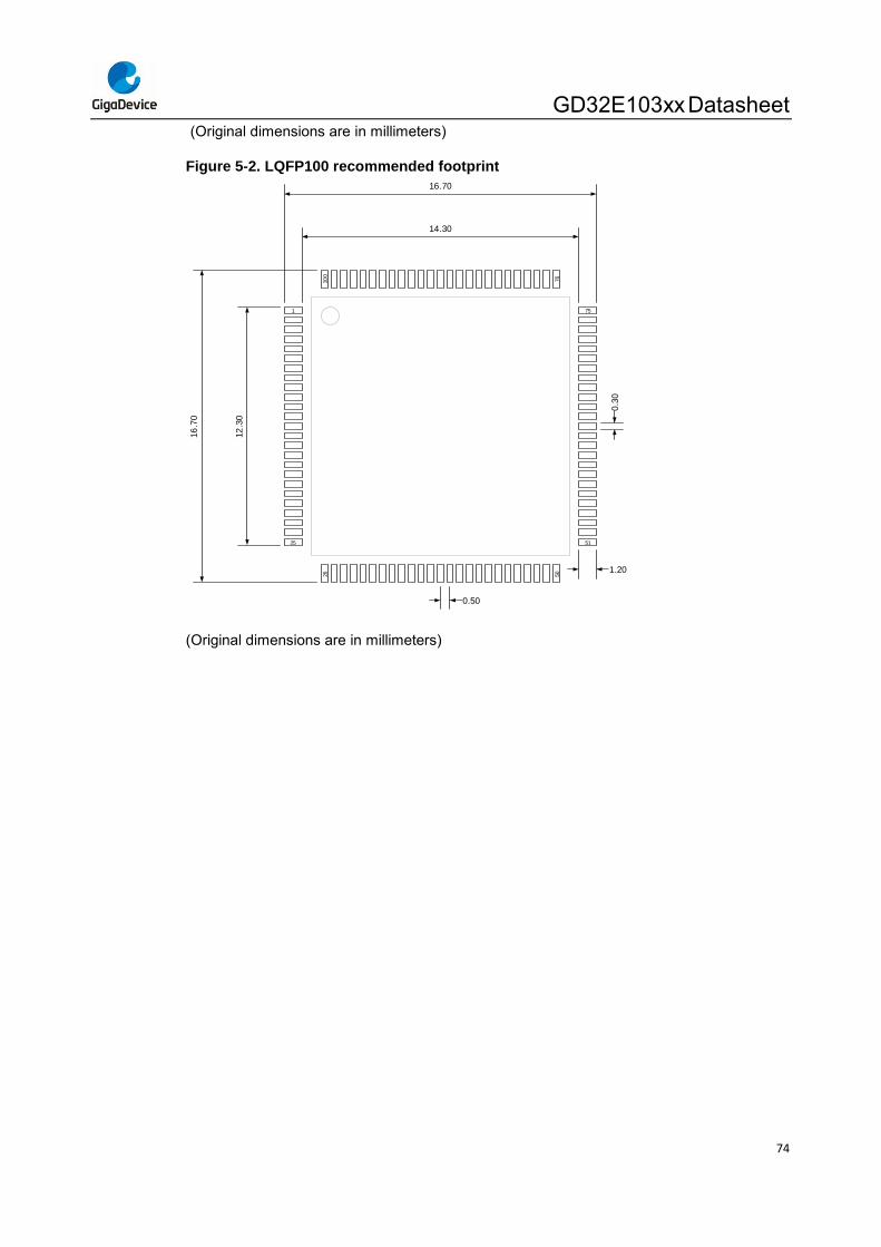
GD32E103xx Datasheet
74
(Original dimensions are in millimeters)
Figure 5-2. LQFP100 recommended footprint
10
0
76
75
51
26
50
1
25
16.70
14.30
16
.70
12
.30
0.50
1.20
0.3
0
(Original dimensions are in millimeters)
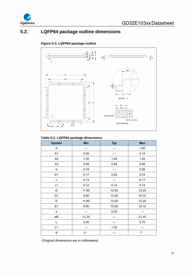
GD32E103xx Datasheet
75
5.2. LQFP64 package outline dimensions
Figure 5-3. LQFP64 package outline
AA2
A1F
A3
θ c
L
L1
DETAIL: F
B B
E1 E
D
D1
eb1
16
32
3348
37
64 17
BASE METAL
WITH PLATING
SECTION B-B
b
b1
c1 c
0.25
eB
Table 5-2. LQFP64 package dimensions
Symbol Min Typ Max
A — — 1.60
A1 0.05 — 0.15
A2 1.35 1.40 1.45
A3 0.59 0.64 0.69
b 0.18 — 0.26
b1 0.17 0.20 0.23
c 0.13 — 0.17
c1 0.12 0.13 0.14
D 11.80 12.00 12.20
D1 9.90 10.00 10.10
E 11.80 12.00 12.20
E1 9.90 10.00 10.10
e — 0.50 —
eB 11.25 — 11.45
L 0.45 — 0.75
L1 — 1.00 —
θ 0° — 7°
(Original dimensions are in millimeters)
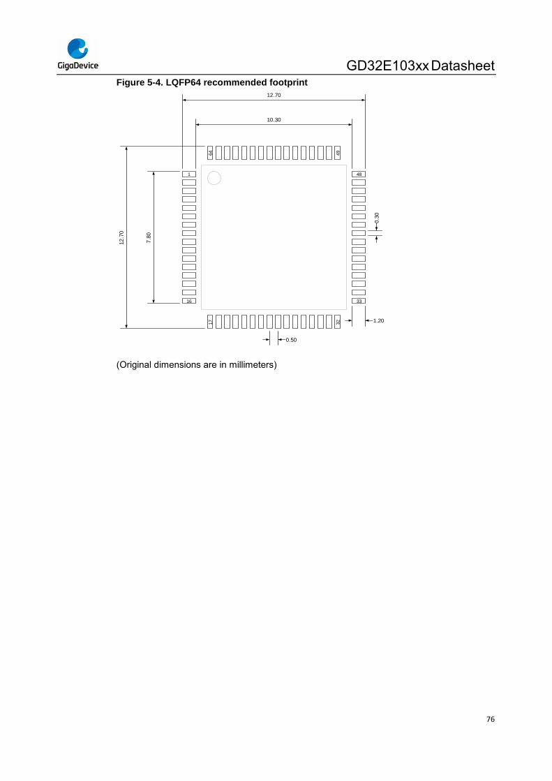
GD32E103xx Datasheet
76
Figure 5-4. LQFP64 recommended footprint
64
49
48
33
17
32
1
16
12.70
10.3012
.70
7.8
0
0.50
0.3
0
1.20
(Original dimensions are in millimeters)
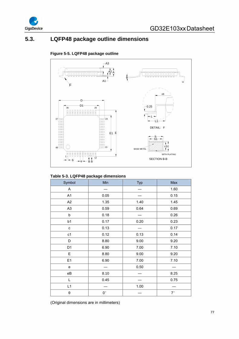
GD32E103xx Datasheet
77
5.3. LQFP48 package outline dimensions
Figure 5-5. LQFP48 package outline
F
DETAIL: F
eB
BASE METAL
WITH PLATING
SECTION B-B
A3
A1
A2 A
θ
c
L
L1
bb1
c1c
0.25
112
24
2536
37
48 13
B
D1
D
E1 E
b e B
Table 5-3. LQFP48 package dimensions
Symbol Min Typ Max
A — — 1.60
A1 0.05 — 0.15
A2 1.35 1.40 1.45
A3 0.59 0.64 0.69
b 0.18 — 0.26
b1 0.17 0.20 0.23
c 0.13 — 0.17
c1 0.12 0.13 0.14
D 8.80 9.00 9.20
D1 6.90 7.00 7.10
E 8.80 9.00 9.20
E1 6.90 7.00 7.10
e — 0.50 —
eB 8.10 — 8.25
L 0.45 — 0.75
L1 — 1.00 —
θ 0° — 7°
(Original dimensions are in millimeters)
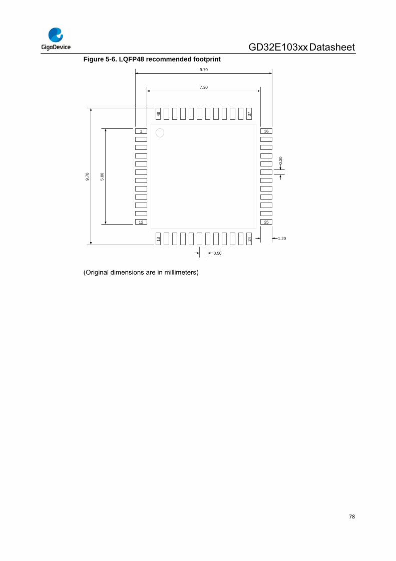
GD32E103xx Datasheet
78
Figure 5-6. LQFP48 recommended footprint
48
37
13
24
25
36
12
1
9.70
7.309
.70
5.8
0
0.3
0
0.50
1.20
(Original dimensions are in millimeters)
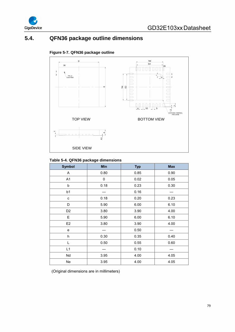
GD32E103xx Datasheet
79
5.4. QFN36 package outline dimensions
Figure 5-7. QFN36 package outline
36
2
1
E
D
PIN 1#
Laser Mark
BOTTOM VIEW
h 2
1
36
L1
L
bb1e
E2
Ne
Nd
D2
TOP VIEW
SIDE VIEW
h
A
c
A1
EXPOSED THERMAL
PAD ZONE
Table 5-4. QFN36 package dimensions
Symbol Min Typ Max
A 0.80 0.85 0.90
A1 0 0.02 0.05
b 0.18 0.23 0.30
b1 — 0.16 —
c 0.18 0.20 0.23
D 5.90 6.00 6.10
D2 3.80 3.90 4.00
E 5.90 6.00 6.10
E2 3.80 3.90 4.00
e — 0.50 —
h 0.30 0.35 0.40
L 0.50 0.55 0.60
L1 — 0.10 —
Nd 3.95 4.00 4.05
Ne 3.95 4.00 4.05
(Original dimensions are in millimeters)
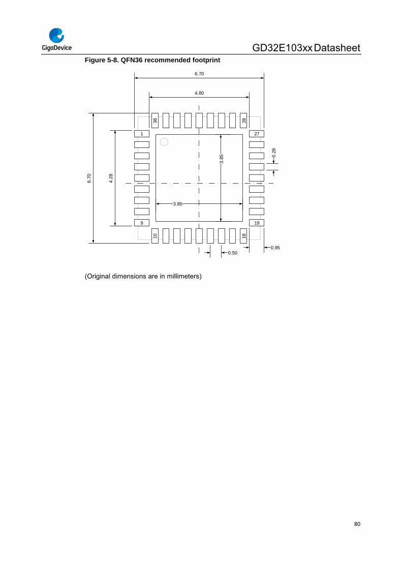
GD32E103xx Datasheet
80
Figure 5-8. QFN36 recommended footprint
6.70
6.7
0
0.500.95
0.2
8
3.85
3.8
5
36
28
10
18
27
19
1
9
4.80
4.2
8
(Original dimensions are in millimeters)
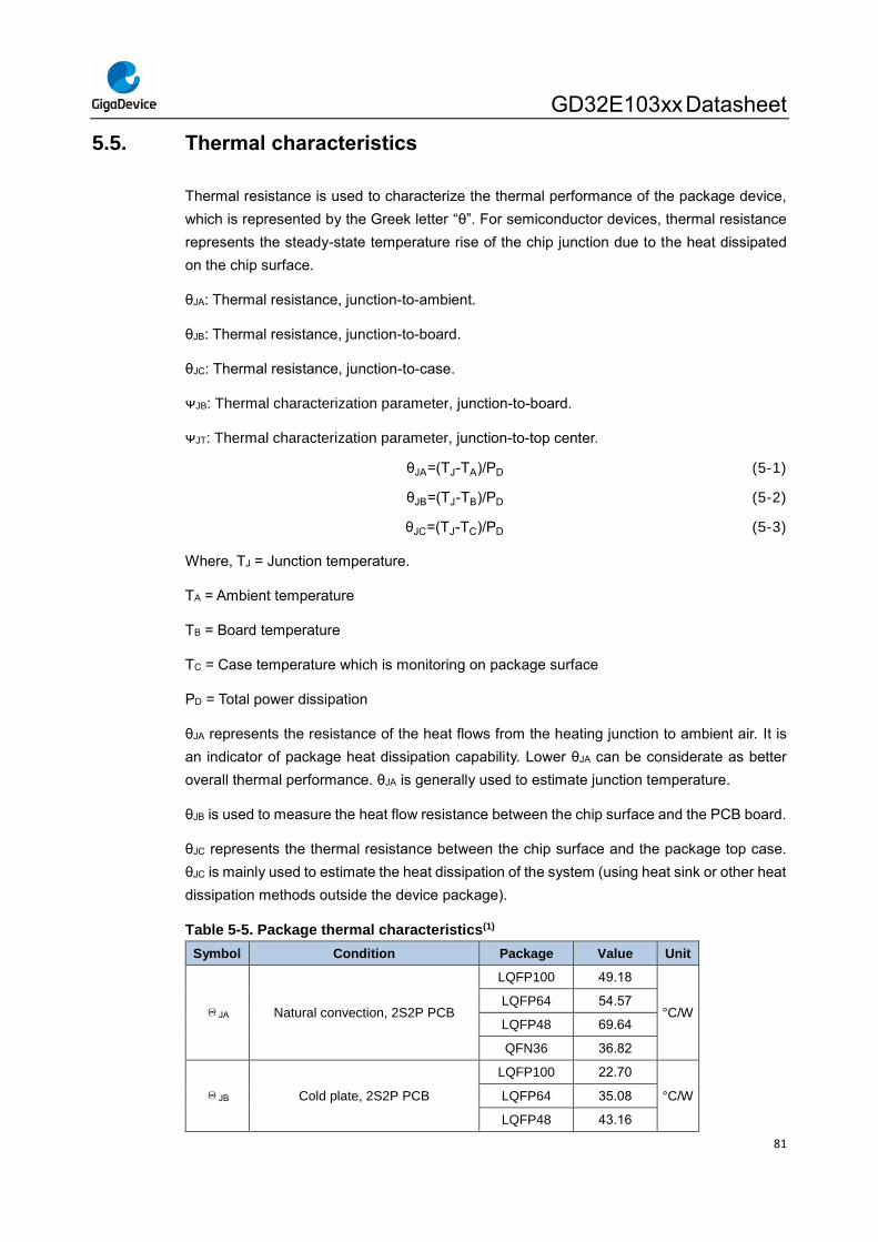
GD32E103xx Datasheet
81
5.5. Thermal characteristics
Thermal resistance is used to characterize the thermal performance of the package device,
which is represented by the Greek letter “θ”. For semiconductor devices, thermal resistance
represents the steady-state temperature rise of the chip junction due to the heat dissipated
on the chip surface.
θJA: Thermal resistance, junction-to-ambient.
θJB: Thermal resistance, junction-to-board.
θJC: Thermal resistance, junction-to-case.
ᴪJB: Thermal characterization parameter, junction-to-board.
ᴪJT: Thermal characterization parameter, junction-to-top center.
θJA=(TJ-TA)/PD (5-1)
θJB=(TJ-TB)/PD (5-2)
θJC=(TJ-TC)/PD (5-3)
Where, TJ = Junction temperature.
TA = Ambient temperature
TB = Board temperature
TC = Case temperature which is monitoring on package surface
PD = Total power dissipation
θJA represents the resistance of the heat flows from the heating junction to ambient air. It is
an indicator of package heat dissipation capability. Lower θJA can be considerate as better
overall thermal performance. θJA is generally used to estimate junction temperature.
θJB is used to measure the heat flow resistance between the chip surface and the PCB board.
θJC represents the thermal resistance between the chip surface and the package top case.
θJC is mainly used to estimate the heat dissipation of the system (using heat sink or other heat
dissipation methods outside the device package).
Table 5-5. Package thermal characteristics(1)
Symbol Condition Package Value Unit
ΘJA Natural convection, 2S2P PCB
LQFP100 49.18
°C/W LQFP64 54.57
LQFP48 69.64
QFN36 36.82
ΘJB Cold plate, 2S2P PCB
LQFP100 22.70
°C/W LQFP64 35.08
LQFP48 43.16
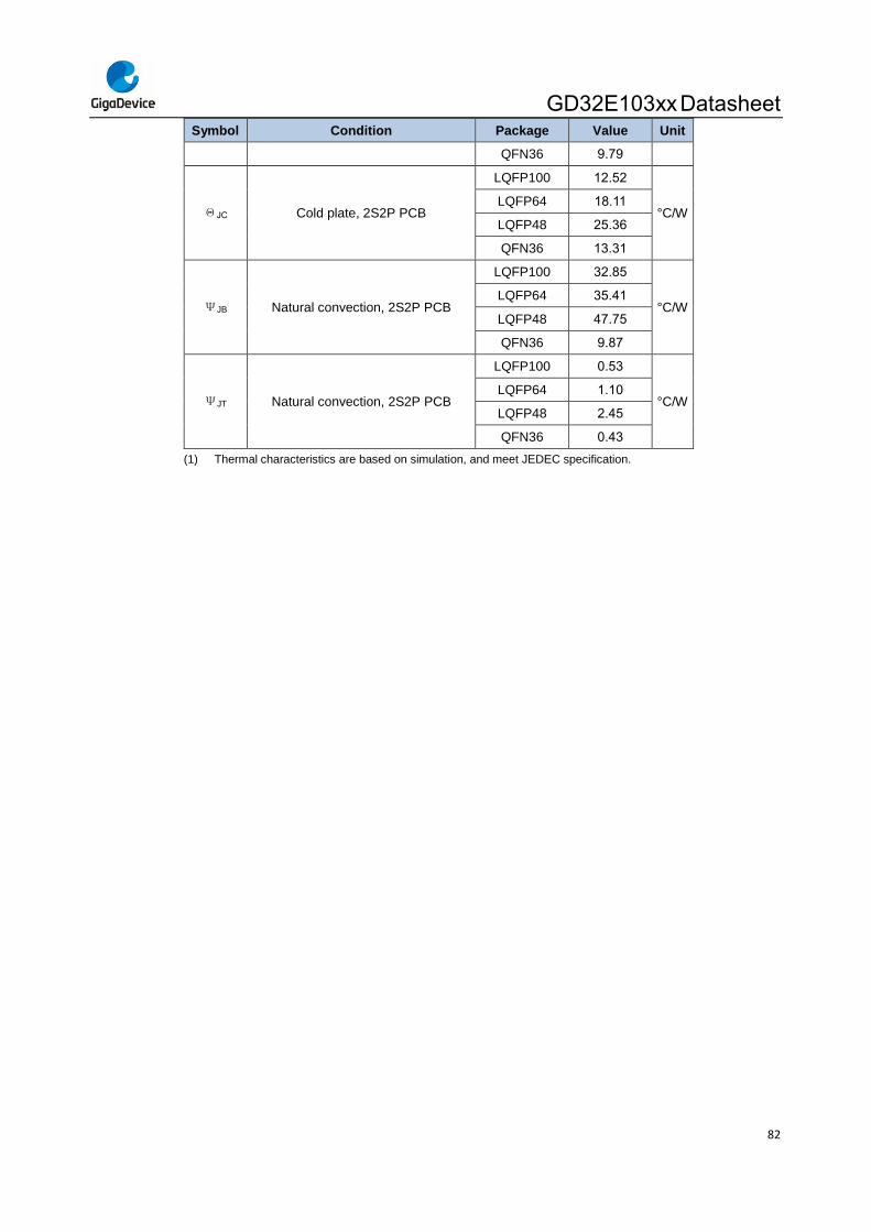
GD32E103xx Datasheet
82
Symbol Condition Package Value Unit
QFN36 9.79
ΘJC Cold plate, 2S2P PCB
LQFP100 12.52
°C/W LQFP64 18.11
LQFP48 25.36
QFN36 13.31
ΨJB Natural convection, 2S2P PCB
LQFP100 32.85
°C/W LQFP64 35.41
LQFP48 47.75
QFN36 9.87
ΨJT Natural convection, 2S2P PCB
LQFP100 0.53
°C/W LQFP64 1.10
LQFP48 2.45
QFN36 0.43
(1) Thermal characteristics are based on simulation, and meet JEDEC specification.
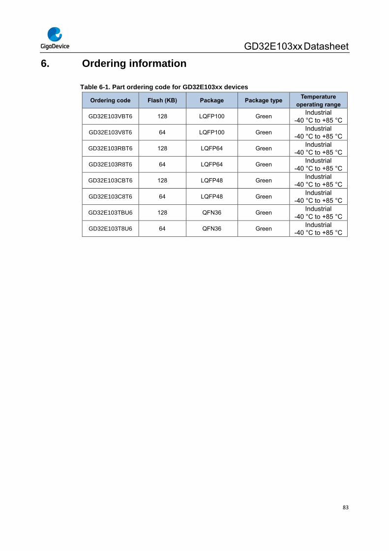
GD32E103xx Datasheet
83
6. Ordering information
Table 6-1. Part ordering code for GD32E103xx devices
Ordering code Flash (KB) Package Package type Temperature
operating range
GD32E103VBT6 128 LQFP100 Green Industrial
-40 °C to +85 °C
GD32E103V8T6 64 LQFP100 Green Industrial
-40 °C to +85 °C
GD32E103RBT6 128 LQFP64 Green Industrial
-40 °C to +85 °C
GD32E103R8T6 64 LQFP64 Green Industrial
-40 °C to +85 °C
GD32E103CBT6 128 LQFP48 Green Industrial
-40 °C to +85 °C
GD32E103C8T6 64 LQFP48 Green Industrial
-40 °C to +85 °C
GD32E103TBU6 128 QFN36 Green Industrial
-40 °C to +85 °C
GD32E103T8U6 64 QFN36 Green Industrial
-40 °C to +85 °C
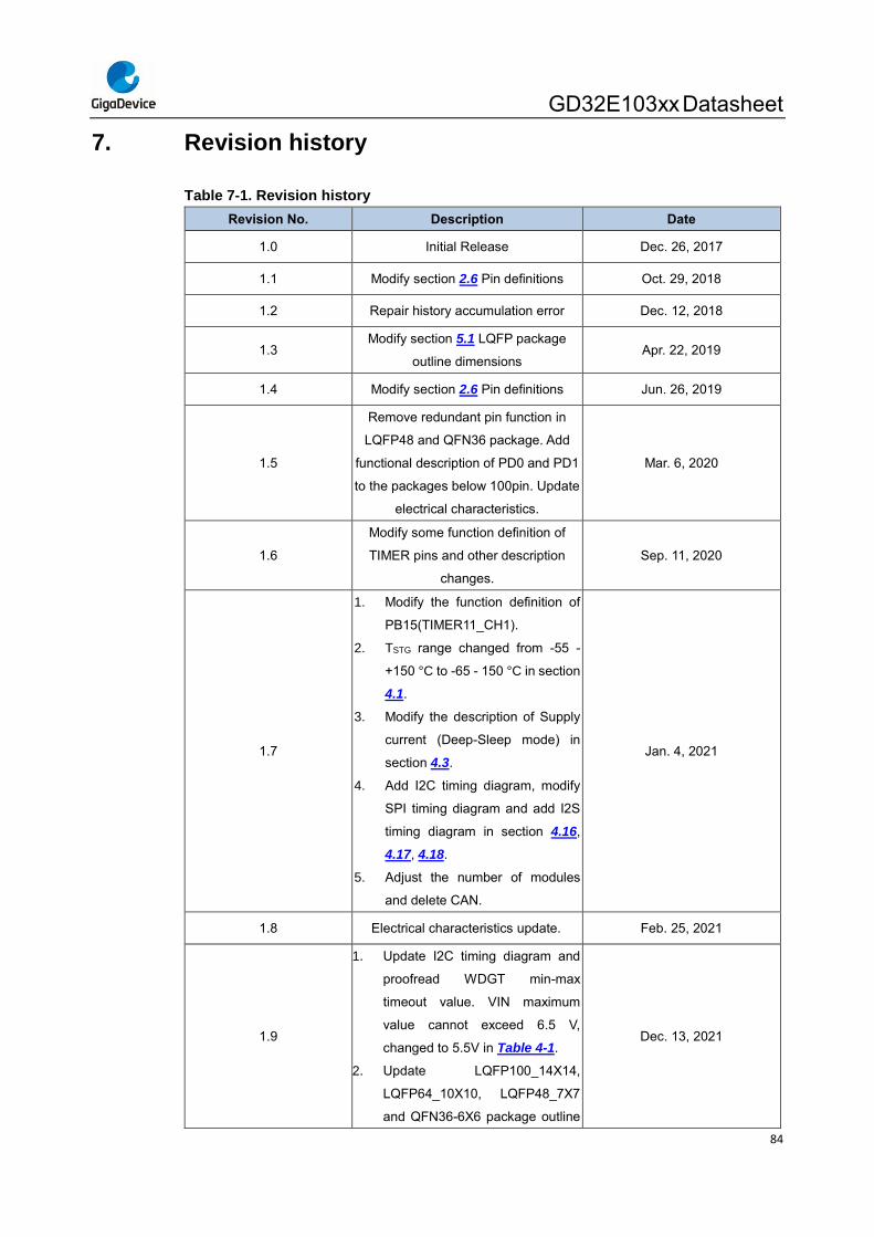
GD32E103xx Datasheet
84
7. Revision history
Table 7-1. Revision history
Revision No. Description Date
1.0 Initial Release Dec. 26, 2017
1.1 Modify section 2.6 Pin definitions Oct. 29, 2018
1.2 Repair history accumulation error Dec. 12, 2018
1.3 Modify section 5.1 LQFP package
outline dimensions Apr. 22, 2019
1.4 Modify section 2.6 Pin definitions Jun. 26, 2019
1.5
Remove redundant pin function in
LQFP48 and QFN36 package. Add
functional description of PD0 and PD1
to the packages below 100pin. Update
electrical characteristics.
Mar. 6, 2020
1.6
Modify some function definition of
TIMER pins and other description
changes.
Sep. 11, 2020
1.7
1. Modify the function definition of
PB15(TIMER11_CH1).
2. TSTG range changed from -55 -
+150 °C to -65 - 150 °C in section
4.1.
3. Modify the description of Supply
current (Deep-Sleep mode) in
section 4.3.
4. Add I2C timing diagram, modify
SPI timing diagram and add I2S
timing diagram in section 4.16,
4.17, 4.18.
5. Adjust the number of modules
and delete CAN.
Jan. 4, 2021
1.8 Electrical characteristics update. Feb. 25, 2021
1.9
1. Update I2C timing diagram and
proofread WDGT min-max
timeout value. VIN maximum
value cannot exceed 6.5 V,
changed to 5.5V in Table 4-1.
2. Update LQFP100_14X14,
LQFP64_10X10, LQFP48_7X7
and QFN36-6X6 package outline
Dec. 13, 2021
GD32E103xx Datasheet
85
and package dimensions,
increase recommended footprint,
increase thermal resistance
description section and parameter
section content.
3. Change the LQFP176 and
LQFP144 POD diagrams, and
add eB parameters to the POD
parameters in packages below
LQFP100 in section 5.1 and
delete the temperature
information in the Condition in the
thermal resistance in section 5.
4. Modify Table 4-1 and Table 4-11.
Delete ETM support.
GD32E103xx Datasheet
86
Important Notice
This document is the property of GigaDevice Semiconductor Inc. and its subsidiaries (the "Company"). This document, including any
product of the Company described in this document (the “Product”), is owned by the Company under the intellectual property laws and
treaties of the People’s Republic of China and other jurisdictions worldwide. The Company reserves all rights under such laws and
treaties and does not grant any license under its patents, copyrights, trademarks, or other intellectual property rights. The names and
brands of third party referred thereto (if any) are the property of their respective owner and referred to for identification purposes only.
The Company makes no warranty of any kind, express or implied, with regard to this document or any Product, including, but not
limited to, the implied warranties of merchantability and fitness for a particular purpose. The Company does not assume any liability
arising out of the application or use of any Product described in this document. Any information provided in this document is provided
only for reference purposes. It is the responsibility of the user of this document to properly design, program, and test the functionality
and safety of any application made of this information and any resulting product. Except for customized products which has been
expressly identified in the applicable agreement, the Products are designed, developed, and/or manufactured for ordinary business,
industrial, personal, and/or household applications only. The Products are not designed, intended, or authorized for use as components
in systems designed or intended for the operation of weapons, weapons systems, nuclear installations, atomic energy control
instruments, combustion control instruments, airplane or spaceship instruments, transportation instruments, traffic signal instruments,
life-support devices or systems, other medical devices or systems (including resuscitation equipment and surgical implants), pollution
control or hazardous substances management, or other uses where the failure of the device or Product could cause personal injury,
death, property or environmental damage ("Unintended Uses"). Customers shall take any and all actions to ensure using and selling
the Products in accordance with the applicable laws and regulations. The Company is not liable, in whole or in part, and customers
shall and hereby do release the Company as well as it’s suppliers and/or distributors from any claim, damage, or other liability arising
from or related to all Unintended Uses of the Products. Customers shall indemnify and hold the Company as well as it’s suppliers
and/or distributors harmless from and against all claims, costs, damages, and other liabilities, including claims for personal injury or
death, arising from or related to any Unintended Uses of the Products.
Information in this document is provided solely in connection with the Products. The Company reserves the right to make changes,
corrections, modifications or improvements to this document and Products and services described herein at any time, without notice.
© 2021 GigaDevice – All rights reserved