Embed Size (px)
Citation preview
PLASMA BONDING OF POLY (DIMETHYL) SILOXANE AND
GLASS SURFACES AND ITS APPLICATION
TO MICROFLUIDICS
by
SHANTANU BHATTACHARYA, B.E.
A THESIS
IN
MECHANICAL ENGINEERING
Submitted to the Graduate Faculty of Texas Tech University in
Partial Fulfillment of the Requirements for
the Degree of
MASTER OF SCIENCE
IN
MECHANICAL ENGINEERING
Approved
December, 2003
ACKNOWLEDGEIVIENTS
I would like to thank my thesis advisor Drs. Shubhra Gangopadhyay and
Jordan Berg for their support, encouragement and valuable guidance throughout
this work. I would not have been able to finish this work without their guidance
and moral support. I am grateful to Dr. Gangopadhyay, La Pierre Chair Professor
at the University of Missouri at Columbia, for giving her valuable time for the
thesis, notwithstanding her extremely busy schedule. I would also like to thank
Dr. Mark Holtz for his valuable comments and suggestions.
I would also like to thank Dr. Arindom Datta of Jack Maddox laboratory
for his help and suggestions throughout this endeavour. Special thanks are due to
all my peers at Jack Maddox Laboratory for being with me and helping me at all
times throughout my stay here.
I have deep gratitude for the help and guidance that I was blessed with
from my family here Finally, I would like to pay my deepest regards to my
parents for bringing me up with values that always help me to succeed in all
endeavors of my life. I dedicate this thesis to my parents.
11
TABLE OF CONTENTS
ACKNOWLEDGEMENTS ii
LIST OF TABLES vi
LIST OF FIGURES vii
CHAPTER
1. INTRODUCTION 1
1. IBackground 1
1.2Processing using soft-lithography 6
1.3Wafer level bonding techniques 6
1.3. IDirect bonding 7
I.40bjectives 7
2. INTRODUCTION TO INDUCTIVELY COUPLED PLASMA AND CONTACT ANGLE 9
2.1 Introduction 9
2.2 Inductively coupled high density plasma system 10
2.2.1 Trion Inductively coupled high density plasma reactor 11
2.3 Contact angle 13
2.3.1 Sessile drop technique 15
2.3.2 Physical reasons for the drop spread 16
3. LITHOGRAPHY BASED POLYMER MOLDING PROCESSES 18
3.1 hitroduction 18
3.2 Materials used 19
111
3.2.1 SU-8 photoresist 19
3.2.2 Poly (dimethyl) siloxane, PDMS 22
3.3 Equipment used 23
3.3.1 Photograph and description of contact angle setup 25
3.4 Glass wafer casting template construction 26
3.4.1 Mask design 26
3.4.2 Wafer cleaning and photoresist coating 27
3.4.3 Exposure of resist coated wafers 31
3.5 Fabrication of blister 36
3.5.1 PDMS molding 36
3.5.2 Imparting hydrophilic properties by exposure to oxygen plasma 37
3.5.3 Fitment of Inlet/Outlet port to the blister 38
4 RESULTS AND DISCUSSION AND CONCLUSION 39
4.1 Introduction 39
4.2 Surface roughness versus bond strength 41
4.2.1 Lapping process 41
4.2.2 Roughness measurement 43
4.3 Measurement of contact angle and bond strength 48
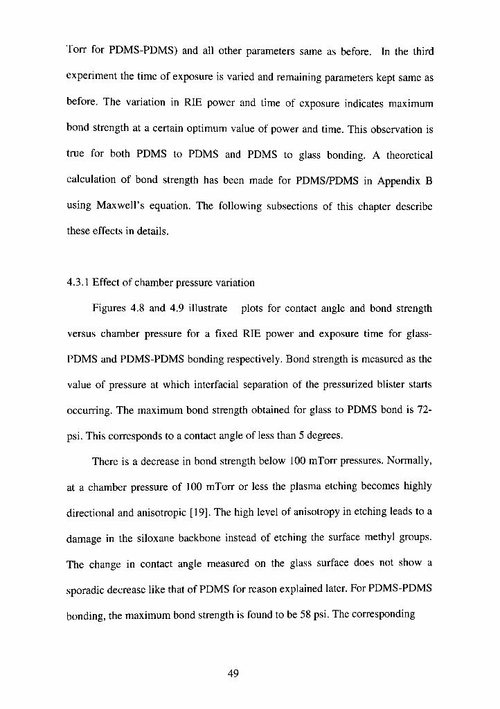
4.3.1 Effect of chamber pressure variation 49
4.3.2 Effect of RIE power variation 52
4.3.3 Effect of time of exposure 55
5 DESIGN CONSIDERATIONS FOR A MICRO REACTOR 64
5.1 Introduction 64
IV
5.2 Micro-mixer mechanisms 68
5.2.1 Passive micro-mixers 69
5.2.1.1 Lamination mixers 69
5.2.1.2 Injection micro-mixer 71
5.2.1.3 Valve micro-mixer 72
5.2.2 Active micro-mixer 73
5.2.2.1 Mixer with pumped fluid inlets 73
5.2.2.2 Ultrasonic mixer 74
5.2.2.3 Magneto hydrodynamic mixers 74
5.3 Experimental (Design, Fabrication and testing) 75
5.3.1 Design 75
5.3.2 Fabrication 77
5.3.3 Testing 79
5.4 Results and discussion 81
6 CONCLUSIONS AND RECOMMENDATION 84
REFERENCES 86
APPENDIX A: Title 93
APPENDIX B: Title 94
LIST OF TABLES
3.1 Chemical composition of SU-8 19
3.2 Spin speeds versus thickness 30
3.3 Pre-exposure or soft bake parameters 30
3.4 Post-exposure bake parameters 31
3.5 Thickness measurements on the molds in Figures 3.5, 3.6, 3.7 and bUster-—35
4.1 Various roughness parameters obtained by Vision 32 44
5.1 Ranges of "Re" values and characterization of the nature of flow 66
A. 1 Important physical properties of SU-8 (Photoresist) 93
VI
LIST OF FIGURES
1.1 Size ranges of micro-fluidic devices 3
1.2 Plot between analyte concentration and sample volume 4
2.1 Schematic of an ICP tube 10
2.2 Schematic of the Trion chamber 12
2.3 Schematic of a contact angle 14
2.4 Infinitesimal expansion of a drop on a surface 14
3.1 Structure of SU-8 molecule 20
3.2 Mechanism of crosslinking of SU-8 21
3.3 Structure of Poly (dimethyl) siloxane 22
3.4 Photograph of the contact angle setup used for experiment 26
3.5 BUster mask 27
3.6 SU-8 mold of thickness 450 microns using multi-layering and single
exposure 33
3.7 SU-8 fabricated on silicon with single layer, single exposure and resist
thickness 150 microns 33
3.8 SU-8 structure of unequal height and its microscopic image fabricated with
multi-layer and multi-exposure 34
3.9 Masks for 1st and 2nd exposure 35
3.I0Aluminum holder for the SU8 master 37
3.11 Schematic of a bUster assembly. 38
4.1 (a~c) PDMS to PDMS failure 40
4.1 (d~f) PDMS to Glass failure 40
4.2 Lapp size used (red bars) versus measured roughness (green bars) 44
4.3 Images of surfaces with different roughness values measured by NTl 100-45
4.4 Bond strength variation of PDMS PDMS with surface roughness 46
4.5 Bond strength variation of glass PDMS with surface roughness 46
4.6 Schematic of PDMS-PDMS and Glass PDMS interface 47
4.7 Contact angle untreated PDMS (109* ) and chemically treated glass (20°)—48
Vll
4.8 Plot of contact angle and bond strength with chamber pressure (range of
variation = 20mTorr) for glass-PDMS 50
4.9 Plot of contact angle and bond strength with chamber pressure (range of
variation= 20mTorr) for PDMS-PDMS bonding 50
4.10 Plot of contact angle and bond strength with RIE power (range of variation
=2W) for glass PDMS bonding 53
4.11 Plot of contact angle and bond strength with RIE power (range of variation
= 2W) PDMS-PDMS 53
4.12 Plot of contact angle and bond strength with time of exposure for Glass-
PDMS 56
4.13 Plot of contact angle and bond strength with time of exposure for PDMS-
PDMS 56
4.14 The hydrophilic silica like surface retarding the bulk molecules 58
4.15 Cracking of the silica like surface promoting the low molar mass molecules to
rise 58
4.16 Various schemes of surface modification in silicone rubbers on corona and
UV radiation 84
4.17 Mechanisms for chain scission reactions (la) 'Back biting' yielding short
cyclics, (lb) random formation of short cyclics along chain, (II) random formation
of high molar mass cyclics along the chain (III) Intermolecular chain scission—59
4.18 Universal trend for variation of chamber pressure and RIE power for Glass-
PDMS bonding 61
4.19 Universal trend for chamber pressure and RIE power for PDMS-PDMS
bonding 61
4.14 Bond reconstruction with increased time of exposure 62
5.1 Three regions of viscous flow (a) laminar flow (Re low) (b) Transition flow
(moderate Re) (c) turbulent flow (high Re 65
5.2 Diffusion coefficient range 67
5.3 Mechanism of a paraUel lamination mixer 69
Vlll
5.4 Sequential mixersl", 2"^ and 3'''' stage of mixing and the 3 dimensional representation of a sequential mixer with 2 different fluid inputs 70
5.5 Injection mixer 72
5.6 Valve micro mixer 72
5.7 Chaotic mixer (a) Two liquids are introduced into the chamber (b) Complete mixing after several pump cycles 74
5.8 Ultrasonic mixer 74
5.9 Different mask designs 76
5.10 Device planning in three layers 77
5.11 Formation of edge effects and effect on bonding 78
5.12 Various micro-mixers 79
5.13 Parallel flow of DI water and highlighter dye (a) and time varying flow by valving(b) 82
5.14 Flow pattern in a "Figure Eight" micro-mixer 83
A2.1 Annular around blister 95
IX

CHAPTER 1
INTRODUCTION
1.1 Background
Microsystems, "literally, mean 'very smaU systems' or 'systems made of
very small components.' They do something interesting and useful. The name
implies no specific way of building them and no requirement that they contain
any particular type of functionality. The name Microelectromechanical systems
(MEMS), on the other hand, takes a position: Micro establishes a dimensional
scale, electro suggests either electricity or electronics (or both). Mechanical
suggests moving parts of some kind. Although the name MEMS suggests limited
domains of work but still the concept of MEMS has outgrown to encompass many
other types of small things, including thermal, magnetic, fluidic, chemical,
biological, and optical devices and systems, not necessarily with moving
(Mechanical) parts [1]. Thus Microsystems engineering is highly
multidisciplinary and involves the manufacturing, testing and packaging of
MEMS equipments. Regular Applications of Microsystems in the aerospace,
automotive, biotechnology, consumer products, defense, environmental protection
and safety, healthcare, pharmaceuticals and telecommunications industry has
created a niche for Microsystems in the society and has led to a growing demand
for the innovation and integration of MEMS and micro-system technology.
From the last decade, the focus in Microsystems research has begun to
shift to fluidic systems [2]. The development of micro-flow sensors, micro-
pumps, and micro-valves dominated the early stage of micro-fluidics research in
the late 1980. The field started developing rapidly in other areas, since the
introduction by Manz et al. at the 5th international conference on solid state
sensors and actuators (transducers '89) which indicated that life sciences and
chemistry are the main application fields of micro-fluidics [3]. Micro-fluidics has
grown since then into a research discipline dealing with the transport phenomena
in fluid based devices at the microscopic length scale. The main advantage of this
discipline is utilizing the scaling laws for new effects and better performance. The
advantages are mainly twin-fold, viz., the microscopic fluid volumes that these
devices can handle and the flexibility of having a large or small sized surrounding
instrumentation with a miniaturization of the space, which handles the fluids. The
field of micro-fluidics is also equally multidisciplinary as compared to
Microsystems technology with the engineers exercising their enabling micro-
technologies and analytical chemists, biochemists, etc., taking advantage of the
new effects and better performance of these technologies. They are interested
primarily in shrinking down the flow channels of chemicals to microns/
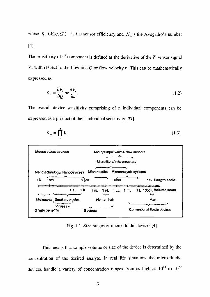
submicron size. Figure 1.1 [4] in the next page shows the size ranges of some
commonly used micro-fluidic devices compared to other objects which are well
perceived by the human mind.
As regards the miniaturization of fluid volumes of these micro-fluidic
devices the sample volume (V) and analyte concentration( A,) are related
inversely as
V = ^ (1.1) Tj^xN^xA.
where //, (0<;7^<1) is the sensor efficiency and A' is the Avogadro's number
[4].
The sensitivity of i"" component is defined as the derivative of the i'*' sensor signal
Vi with respect to the flow rate Q or flow velocity u. This can be mathematically
expressed as
The overall device sensitivity comprising of n individual components can be
expressed as a product of their individual sensitivity [37].
K . = n K , . (1.3)
MiCROFiuiOJC D£V»CES Micropufnps/ valves/ flow sensors
MiCfOfitters/ miaoreactors
Nanotechnotogy/ Nanotfevices? Miooneedtes MN:roanalysis systems - > 4—-*—» . f ^
lA Inm 1 (im imm l m Lengthscate I ' •••-•••tw-wn, (•• ) t 1 I \ \ s \ m
l a l iflL 1 pL inl 1 nL ImL 1L 1000 tVolume scale ^ .. . t ^ * * _ > LyJ
Motecutes SrrK*e partkdes Human hair Man
Viruses •*-.- ,,..- -» "^ OTwe«<»JECTs Bacterid ConveittJonal fluklk: devices
Fig. 1.1 Size ranges of micro-fluidic devices [4]
This means that sample volume or size of the device is determined by the
concentration of the desired analyte. In real life situations the micro-fluidic
devices handle a variety of concentration ranges from as high as 10 to 10"
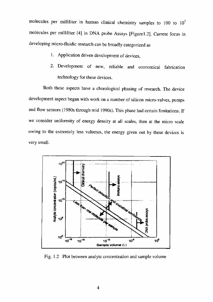
molecules per milliliter in human clinical chemistry samples to 100 to 10
molecules per milliliter [4] in DNA probe Assays [Figurel.2]. Current focus in
developing micro-fluidic research can be broadly categorized as
1. Application driven development of devices,
2. Development of new, reliable and economical fabrication
technology for these devices.
Both these aspects have a chorological phasing of research. The device
development aspect began with work on a number of silicon micro-valves, pumps
and flow sensors (1980s through mid 1990s). This phase had certain limitations. If
we consider uniformity of energy density at all scales, then at the micro scale
owing to the extremely less volumes, the energy given out by these devices is
very small.
10"" ior" irf Sampte volume (L)
Fig. 1.2 Plot between analyte concentration and sample volume
Also, the surface-to-volume ratio being length (microns) inverse, the
surface area automatically becomes huge in comparison to the volume. Large
surface area means large viscous forces, which in turn require a large actuation
level, which is normally provided by external sources. The second phase (mid-
1990s onward) concentrated on non-mechanical actuation schemes such as
electro-kinetic flows, surface tension driven flows, electromagnetic forces and
acoustic streaming effects. This phase has led into the gradual shift of micro-
fluidic applications from conventional field, such as flow control, chemical
analysis, biomedical diagnostics, and drug discovery to newer applications such
as distributed energy supply, thermal management and chemical production.
The second aspect in micro-fluidic research is developing a suitable
fabrication process. Similar to the prior aspect, this technology development also
had a paradigm shift from development of micro-fluidic devices in silicon (up to
mid-1990s) to use of plastic micro-machining on an extremely biocompatible
material called Poly (dimethyl) Siloxane (hence forth called PDMS). A problem
faced worldwide in such micro-fabrication process is the absence of a well-
defined study of the bonding strength between the various layers used to make
these devices. Although most of the research papers mention the Oxygen Plasma
activation of participating surfaces leading to strong chemical (Silanol) bonds
between them [4, 5], yet these papers only define a certain set of parameters,
which are specific to their plasma generating setup and not valid in general [6, 7].
With these newer and easier fabrication techniques being widely used in the
laboratory and industry level, an important requirement of all the micro fluidics/
biosensors research and industry is the development of a general regime, which
defines a systematic method of gauging the bond strength between the
participating surfaces. This enhances the reliability of the devices and also gives a
structured approach to its future large-scale manufacturing.
1.2 Processing using Soft-lithography
Soft lithography can be used for rapid prototyping of micro-fluidic
devices. This is- done by fabricating the master using SU8 negative tone photo
resist using contact printing. In contact printing the mask is placed directly over
the photo resist coated wafer. A 10:1 ratio of a silicone rubber and a curing agent
is poured over the SU8 pattern kept in a well-milled aluminum plate. The mixture
is cured and thus the pattern gets transferred on the surface of the PDMS bulk [9].
After the pattern transfer process using the above techniques, the
devices are given shape by stacking different layers above each other [10, 11]. By
this technique enclosed chambers and fluidic channels can be made between
various substrates using a variety of different wafer level bonding techniques.
1.3 Wafer level bonding techniques
Wafer bonding is used to join two or more layers of any MEMS device.
There are three main categories of wafer bonding techniques:
• Field-assisted bonding,
• Bonding with an intermediate layer,
• Direct bonding.
As direct bonding is used for most of this work therefore we will look into
details of direct bonding in the following section.
1.3.1 Direct bonding
This category of bonding involves the bonding of two substrates of same
material to one another. A variety of substrates like glass, silicon, polymers,
ceramics and metals can be bonded to each other directly.
There are many polymers that can be normally bonded at temperatures
above their glass transition temperature. Some polymers with low surface energy
as PDMS can be bonded to itself and to glass after a surface activation with
oxygen plasma. The mechanism of bonding in this involves the oxidation of the
surface layer, which increases the concentration of hydroxyl groups, and this
leads to the formation of strong intermolecular bonds. As bonds formed by this
method is irreversible, it is commonly used in micro-fabrication of fluidic
devices. A common application area of such techniques of fabrication lies in the
building of a micro-mixer. PDMS and glass being totally transparent provides a
convenient visualization of fluid mixing at the micro-scale.
1.4 Objectives
In this study, we have explored the possibility of the existence of a
common scale, which can be used to gauge bond strength between various
surfaces. We found that the changes in wettability of surfaces owing to various
levels of plasma exposure can be a useful parameter to gauge the bond strength.

Surface roughnesses of the participating surfaces in such bondages have also been
plotted with bond strengths.
A good correlation is obtained between contact angle of de-ionized water
(a direct measure of wettability) on the PDMS and glass surfaces based on various
dosages of Oxygen Plasma treatment in an inductively coupled high density
plasma system and the bond strength calculated using the standardized bUster test
[12].
Finally, this fabrication technique is utilized in building and packaging of
a pneumatically valved, gravity fed twin fluid micro-reactor on a 2.5 inches
diameter soda-lime glass wafer. Several designs are intuitively fabricated and
mixing is observed qualitatively. The Reynolds number for such flows is
calculated and mixing behavior studied at low Reynolds number. We will first
start by description of plasma and its associated processes followed by theoretical
description of wettability and contact angle. This will be followed by the
description of processing aspects of micro-fabrication. The final part will be a
discussion of trend between contact angle and bond strength followed by an
investigation in various design considerations for a micro-mixer.
CHAPTER 2
INTRODUCTION TO INDUCTIVELY COUPLED PLASMA AND CONTACT ANGLE
2.1 Introduction
Plasma is defined as a system of electrical neutrality composed of positive
and negative charge carriers. In 1928, Langmuir and Tonks, at the General
Electric Research Laboratory [15], first coined the term "plasma" to describe
ionized gas. The first form of plasma observed was the glow discharge, in which
an equal no. of positive ions and electrons are present. Plasmas differ greatly in
many respects based on several parameters like pressure, charge particle density,
and temperature. Furthermore, the boundary conditions as well as the presence of
external electric or magnetic fields yield different forms of plasma. If the positive
ions are fixed, as in a solid, and the electrons are mobile, the system may be
referred to as solid-state plasma. Liquid plasmas exist in salt solutions in which
the positive and negative ions move separately. The gaseous state of plasma is one
in which the free electric charges can move through the gas, usually under the
influence of an electric field, which is the agent causing ionization of the gas in
question. Based on their production techniques, the plasmas can be categorized
into the following:
• DC glow discharge,
• Radio-frequency discharge,
• Magnetically enhanced plasma.
As inductively coupled plasma is mostly used is used for this work
therefore we will briefly investigate its generation and also the equipment used.
2.2 Inductively coupled high density plasma system
Inductively coupled plasma is generated when a confined gas is
surrounded by solenoid coil through which a high frequency current is passed.
The RF magnetic field of the coil is directed towards the axis of the coil and
induces a vortex electric field. The field couples to electrons, produces electron
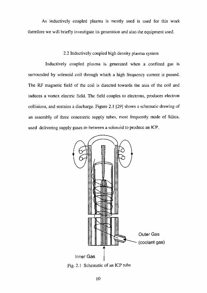
collisions, and sustains a discharge. Figure 2.1 [29] shows a schematic drawing of
an assembly of three concentric supply tubes, most frequently made of Silica,
used delivering supply gases in-between a solenoid to produce an ICP.
Outer Gas
(coolant gas)
Inner Gas
Fig. 2.1 Schematic of an ICP tube
10
The assembly of the tubes is setup in a water-cooled coil of an RF
generator. The torch comprises of three tubes called the 'inner tube', the
'intermediate tube' and the 'outer tube.' Flowing gases are introduced into the
torch, the RF field is switched on and the gases in the coil region are made
electrically conductive by Tesla sparks [28]. This creates plasma, if the gas
streams follow a particular rotationally symmetrical pattern. Once the plasma is
formed it is sustained by inductive heating of the flowing gas in a way similar to
the inductive heating of a metallic cylinder placed in the induction coil in which
the RF currents flowing through the coil, generate oscillating magnetic fields with
lines of force axially oriented inside the coil. These induced magnetic fields
generate in turn high frequency, annular electric currents in the conductor, which
is then heated as a result of its ohmic resistance. If the conductor is a flowing
medium, such as a gas, an insulating tubular confinement is required to prevent
short-circuiting by extending into the coil. On the other hand, the gas flow should
be made so that a thin sheath of cold gas separates the plasma from the outer
confinement tube in order to prevent the latter from melting. The thermal isolation
of plasma can be achieved by using a tangentieiUy introduced gas flow called
coolant gas in the outer tube. The outer gas is introduced tangentially to produce a
low-pressure area at the center of the torch and cause recirculation of the plasma
giving a continuous supply of ions in the coil region.
11
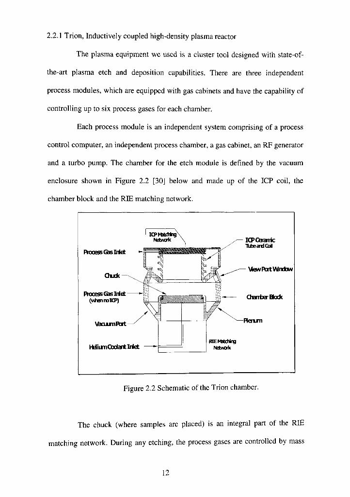
2.2.1 Trion, Inductively coupled high-density plasma reactor
The plasma equipment we used is a cluster tool designed with state-of-
the-art plasma etch and deposition capabilities. There are three independent
process modules, which are equipped with gas cabinets and have the capability of
controlling up to six process gases for each chamber.
Each process module is an independent system comprising of a process
control computer, an independent process chamber, a gas cabinet, an RF generator
and a turbo pump. The chamber for the etch module is defined by the vacuum
enclosure shown in Figure 2.2 [30] below and made up of the ICP coil, the
chamber block and the RIE matching network.
PnxBSBQaslrtA
Oujc
RtxESsGasIiilet (whainoKF)
VtounRxt
HeliimCbclartlrlefc
VCPtVaiipg Networic ia>Oeramc
TiteandODil
VtewPortVUrelow
OBrrtierBkxk
Herun
RiENUdvig NetwDk
Figure 2.2 Schematic of the Trion chamber.
The chuck (where samples are placed) is an integral part of the RIE
matching network. During any etching, the process gases are controlled by mass
12
flow controllers (MFC). A scrubber is an integral part of the system that acts as an
exhaust for waste gases generated in the process chamber. When the RF
generators for both the RIE and ICP are turned on, plasma is created in the
chamber. The ICP is used as the primary plasma source and creates plasma by
inductively coupling the RF power through the ceramic tube. The idea is to use
the ICP to generate high-density plasma in the ceramic tube above the chuck.
Then, RF power (also known as the reactive ion etching power) is supplied to the
chuck to generate the bias. This bias voltage is the driving factor in accelerating
the ions to the sample thereby increasing etch rate and anisotropy.
2.3 Contact angle
The surface tensions of solid vapor interfaces and solid liquid interfaces are
important parameters in many areas of applied science and technology. These
interfacial tensions are responsible for the behavior and properties of commonly
used materials. However, because of the absence of mobility, a solid phase is very
different from a liquid fluid interface, and hence solid interface tensions cannot be
measured directly. Therefore, an indirect method, by measuring a contact angle of
a liquid drop on solid surface is required. Under this method the angle between a
drop of solvent and a solid is measured and from this we can estimate the surface
energy. Surface energies have direct consequences on properties such as adhesion,
friction and wettability. Figure 2.3 shows a schematic of the contact angle of a
droplet with a solid surface. The contact angle of a drop of water on the surface is
13
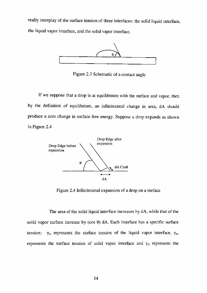
really interplay of the surface tension of three interfaces: the solid liquid interface,
the liquid vapor interface, and the solid vapor interface.
Figure 2.3 Schematic of a contact angle
If we suppose that a drop is at equilibrium with the surface and vapor, then
by the definition of equilibrium, an infinitesimal change in area, dA should
produce a zero change in surface free energy. Suppose a drop expands as shown
in Figure 2.4
Drop Edge before expansion
Drop Edge after expansion
dA Cose
•* •
dA
Figure 2.4 Infinitesimal expansion of a drop on a surface
The area of the solid liquid interface increases by dA, while that of the
solid vapor surface increase by (cos 9) dA. Each interface has a specific surface
tension: yw represents the surface tension of the liquid vapor interface, YSV
represents the surface tension of solid vapor interface and ysi represents the
14
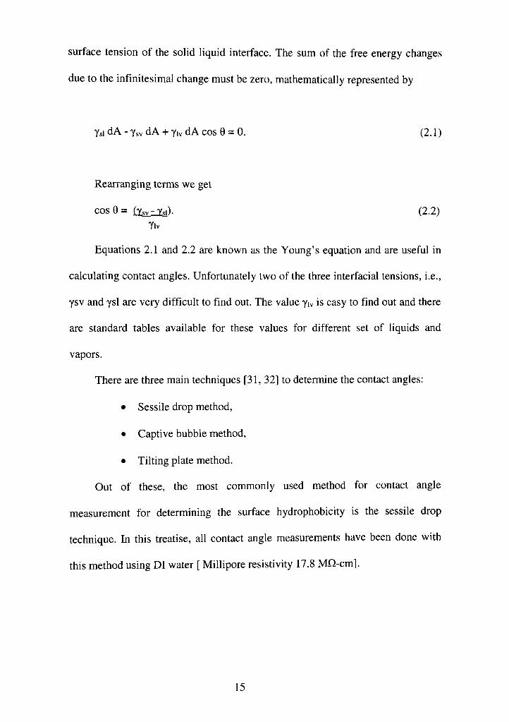
surface tension of the solid liquid interface. The sum of the free energy changes
due to the infinitesimal change must be zero, mathematically represented by
Ysi dA - Ysv dA + Yiv dA cos 6 = 0. (2.1)
Rearranging terms we get
cos 9 = (Ygy jsi)- (2.2) Yiv
Equations 2.1 and 2.2 are known as the Young's equation and are useful in
calculating contact angles. Unfortunately two of the three interfacial tensions, i.e.,
ysv and ysl are very difficult to find out. The value y^ is easy to find out and there
are standard tables available for these values for different set of liquids and
vapors.
There are three main techniques [31, 32] to determine the contact angles:
• Sessile drop method,
• Captive bubble method,
• Tilting plate method.
Out of these, the most commonly used method for contact angle
measurement for determining the surface hydrophobicity is the sessile drop
technique. In this treatise, all contact angle measurements have been done with
this method using DI water [ Millipore resistivity 17.8 MQ-cm].
15
2.3.1 Sessile drop technique
This method is based on the equilibrium of an axisymmetric sessile drop on
a flat, horizontal, smooth, homogeneous, isotropic, and rigid solid. Contact angles
on polymer surfaces are not only influenced by the interfacial tensions but also by
many other phenomena, such as surface roughness, chemical heterogeneity,
molecular orientation, swelling, and partial solution of the polymer or low-
molecular constituents in the polymer material. However, if the question is to
compare contact angles of pieces of an identically prepared surface as in
experiments in this treatise, then these factors can be neglected.
2.3.2 Physical reasons for the drop spread
Atoms are held in molecular structures by two types of bonds ionic and
covalent. Similarly molecules are held in larger structures by (liquids and solids)
by cohesive or adhesive forces, which are termed as intermolecular forces. The
term adhesion arises due to the attraction that the molecules of one material feel to
the molecules of the other material. Cohesion forces on the other hand are forces
between molecules of the same material. Surface tension of any liquid is the
measurement of its cohesion. When a liquid is allowed to interact with a solid or
gas, the forces of adhesion come into play.
The intermolecular forces are mainly electrostatic in nature wherein the
strong forces arise due to covalent, ionic and metallic bonding. There are three
weak forces also known as the van-der-Waals forces, which mainly arise from
hydrogen bonding, Dipole-Dipole interactions, and London Dispersion forces. In
16
the case of the spread of droplets, these weak van-der-Waals forces mainly
contribute to the force of adhesion. Among these, the hydrogen bond is the
strongest weak bond, wherein the positively charged hydrogen end of one
molecule is attracted to a negatively charged end of another molecule, which must
be an extremely electronegative element. The medium strength dipole-dipole
interactions exist between neutral, polar molecules where, the positive end of one
molecule is attracted to the negative end of another molecule. The weakest
strength London Dispersion forces arise due to random motion of electrons
resulting in an instantaneous polarity on the atom causing a very weak dipole
moment resulting in a weak force.
If the forces of adhesion are not stronger than the forces of cohesion as in
the case of untreated PDMS comprising of non-polar surface methyl groups, the
forces of cohesion in-between the water molecules being greater generate a net
upward pull to bead the water droplet on the surface. In a drop of water on treated
PDMS surface, which comprises of an excess of surface silanol groups, the
downward pull due to a prominence of the van-der-Waals forces, tries to wet the
surface.
17
CHAPTER 3
LITHOGRAPHY-BASED POLYMER MOLDING PROCESSES
3.1 Introduction
In this study, a specific lithography based polymer-molding process for the
low cost fabrication of micro-channels and blisters capable of withstanding high
injection pressures have been developed. Fabrication is done over a large range of
dimensions from 50 to 500 microns. This fabrication process is further used to
develop a pneumatically valved twin fluid gravity fed micro mixer.
Photolithography is used to pattern a 10 cm diameter soda-lime glass wafer,
which acts as a mold from which, an organic polymer poly (dimethyl) siloxane
(PDMS) can be replica molded. This entire process from design conception to the
completion of the intended design takes about 5-6 hours.
Micro-channels are generally fabricated by directly micro-machining silicon
or glass [32]. Micro-fabrication over glass or silicon are often expensive, time
consuming and labor intensive. For micro-fabricated devices to ease their way in
the scientific community, the cost, ease of fabrication and functionality need to be
addressed [33]. Transparent, visco-elastic organic polymer, poly (dimethyl)
siloxane can be used as an alternative for micro-fabrication to the costlier and
time-consuming methods over glass and silicon. The patterned glass wafer is used
as a casting template for an organic polymer, poly (dimethyl) siloxane (PDMS),
stamp in the process that is relatively simple, quick and inexpensive. Use of
replica molding process allows for the casting of numerous PDMS devices from
18
one patterned glass wafer. These stamps are then bonded to each other using
oxygen plasma thus forming the device assembly. Patteming of the glass wafer is
done using SU8 2075 a negative photoresist and a mask printed on a high-
resolution printer.
3.2 Materials used
3.2.1 SU-8 Photoresist
SU-8 2000 is a high contrast, epoxy based photo resist designed for micro-
fabrication processes where a thick, chemically and thermally stable image is
desired. As it is used as a template for the PDMS which solidifies on heating to
high temperature therefore thermal stability of the resist is important to get high
definition structures. Table 3.1 comprises of the chemical ingredients of SU8 with
their respective concentration.
Table 3.1 Chemical composition of SU-8 [34]
S.No.
1
2
3
Chemical Ingredient
Gamma Butyrolactone
Propylene carbonate
Epoxy resin
%age
22-60
1-5
35-75
Primarily SU-8 consists of a photosensitized epoxy resin or photoplastic
dissolved in gamma butyrolactone and a proprietary photo acid generator, which
generates hydrofluoric acid upon exposure. The photo generated acid cleaves the
19
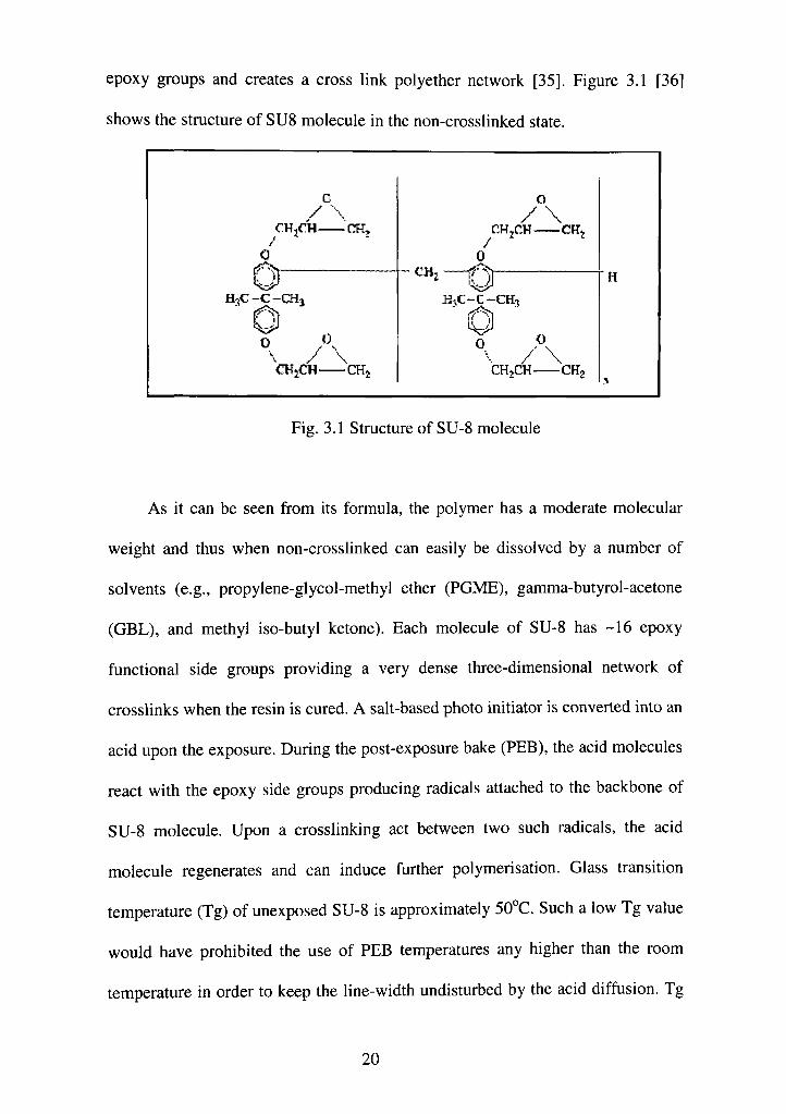
epoxy groups and creates a cross link polyether network [35]. Figure 3.1 [36]
shows the structure of SU8 molecule in the non-crosslinked state.
o
0
H^C ~C — CHj
o 0 \ / \
/
O / \
CHn
HjC-C-CH;,
0 . / \
H
Fig. 3.1 Structure of SU-8 molecule
As it can be seen from its formula, the polymer has a moderate molecular
weight and thus when non-crosslinked can easily be dissolved by a number of
solvents (e.g., propylene-glycol-methyl ether (PGME), gamma-butyrol-acetone
(GBL), and methyl iso-butyl ketone). Each molecule of SU-8 has -16 epoxy
functional side groups providing a very dense three-dimensional network of
crosslinks when the resin is cured. A salt-based photo initiator is converted into an
acid upon the exposure. During the post-exposure bake (PEB), the acid molecules
react with the epoxy side groups producing radicals attached to the backbone of
SU-8 molecule. Upon a crosslinking act between two such radicals, the acid
molecule regenerates and can induce further polymerisation. Glass transition
temperature (Tg) of unexposed SU-8 is approximately 50°C. Such a low Tg value
would have prohibited the use of PEB temperatures any higher than the room
temperature in order to keep the line-width undisturbed by the acid diffusion. Tg
20
value of the polymer begins to grow rapidly with the increase of the number of
crosslinks thus dramatically decreasing the acid diffusion rate. For fully
crosslinked SU-8, Tg exceeds 200°C. In this way, the polymerisation process is
contained in the areas of the resist, where the initial acid concentration was
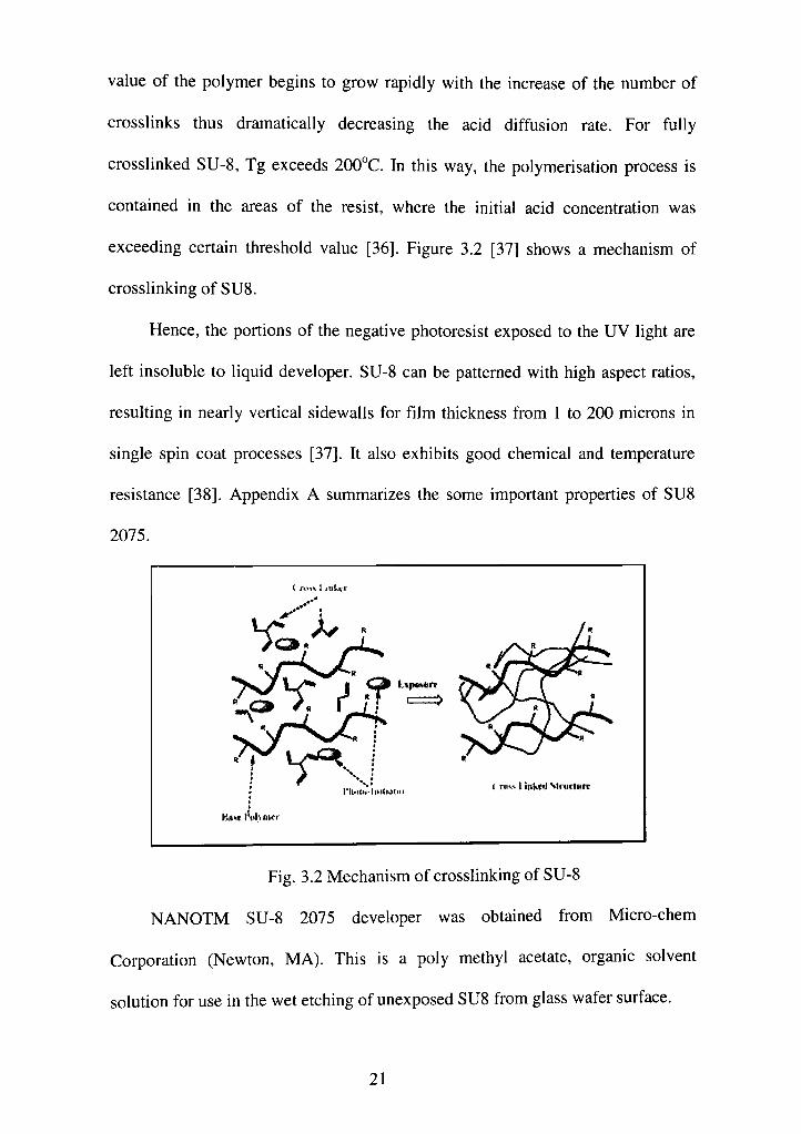
exceeding certain threshold value [36]. Figure 3.2 [37] shows a mechanism of
crosslinking of SU8.
Hence, the portions of the negative photoresist exposed to the UV light are
left insoluble to liquid developer. SU-8 can be patterned with high aspect ratios,
resulting in nearly vertical sidewalls for film thickness from 1 to 200 microns in
single spin coat processes [37]. It also exhibits good chemical and temperature
resistance [38]. Appendix A summarizes the some important properties of SU8
2075.
i -rt!>i*i I (iil^r
.' I'h'itif-lnHMiKf * r i i " t il»li«l 'MnicHirt
BM* t'AflK-r
Fig. 3.2 Mechanism of crosslinking of SU-8
NANOTM SU-8 2075 developer was obtained from Micro-chem
Corporation (Newton, MA). This is a poly methyl acetate, organic solvent
solution for use in the wet etching of unexposed SU8 from glass wafer surface.
21
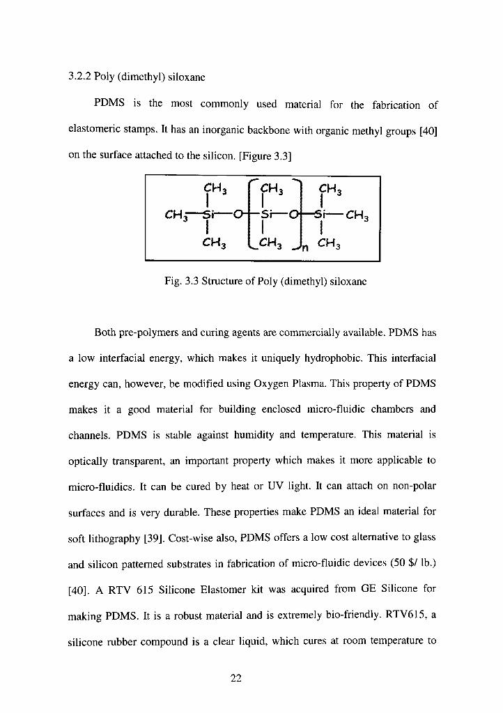
3.2.2 Poly (dimethyl) siloxane
PDMS is the most commonly used material for the fabrication of
elastomeric stamps. It has an inorganic backbone with organic methyl groups [40]
on the surface attached to the silicon. [Figure 3.3]
Fig. 3.3 Structure of Poly (dimethyl) siloxane
Both pre-polymers and curing agents are commercially available. PDMS has
a low interfacial energy, which makes it uniquely hydrophobic. This interfacial
energy can, however, be modified using Oxygen Plasma. This property of PDMS
makes it a good material for building enclosed micro-fluidic chambers and
channels. PDMS is stable against humidity and temperature. This material is
optically transparent, an important property which makes it more applicable to
micro-fluidics. It can be cured by heat or UV light. It can attach on non-polar
surfaces and is very durable. These properties make PDMS an ideal material for
soft lithography [39]. Cost-wise also, PDMS offers a low cost alternative to glass
and silicon patterned substrates in fabrication of micro-fluidic devices (50 $/ lb.)
[40]. A RTV 615 Silicone Elastomer kit was acquired from GE Silicone for
making PDMS. It is a robust material and is extremely bio-friendly. RTV615, a
silicone rubber compound is a clear liquid, which cures at room temperature to
22
high strength silicone rubber with the addition of curing agents. This two-
component system comes with curing agent in matched kits, which is designed for
use at a convenient 10:1 ratio by weight.
The compound is clear and colorless, moderately viscous; easily pourable
liquid with nominal viscosity ranging between 3000 and 7000 cps. [40] RTV615,
silicone rubber compounds have been used for protection of electronic
components and assemblies against shock, vibration, moisture, ozone, dust,
chemicals, and other environmental hazards by potting or encapsulation of the
components and assemblies.
PDMS also presents a number of drawbacks, such as volume change and
elastic deformation. Thus, PDMS structures should consist of shrinkage
allowance in design phase. A too high aspect ratio for PDMS structures leads to a
pairing effect, in which two parallel structures attach to each other.
3.3 Equipment used
The following equipment is used for the lithography-based polymer molding
process. These are sonicator, spin table, mask aligner, convection oven, agitator, a
vacuum pump and desiccator. The sonicator is mainly used for cleaning of the
glass surface in organic solvent by giving ultrasonic excitation through a liquid
medium (ordinary water, in our case). Ultrasonic liquid processing is a highly
valuable methodology in the laboratory. High intensity (20 kHz and above)
ultrasonic generation is sufficientiy powerful to achieve useful liquid processing
in a wide variety of applications [43].
23
In liquid, the rapid (i.e., 20 kHz) vibration of the container causes cavitation,
the formation and violent collapse of microscopic bubbles.
The collapse of thousands of cavitation bubbles releases tremendous energy in the
cavitation field. Objects and surfaces that are within the cavitation field are
cleaned by the released energy [44]. The Maddox lab sonicator is a Sonic Bath
Branson 1510 make of M/s Analytical Instruments.
The spin table is used for photoresist coating on glass substrate. The
Maddox laboratory has a EC 10IDT Digital Photo Resist Spinner. It is a high
acceleration, high torque, electronically regulated, auto-cycle controlled, and
automatically braked spinner. The motor has a hole through the shaft for the
application of vacuum to the substrate held by the chuck, which is attached to the
spinner shaft, with the purpose of securing the substrate to the shaft while
spinning [45].
The Maddox mask aligner, PLA 501 F, is a contact mask aligner, which can
accommodate up to 6 inches round wafers. It has both automatic and manual
wafer loading/unloading system. The mask aligner is used in our processing for
contact printing, which is achieved by aligning a photo-mask printed over a
transparency using a 3200 dpi black and white printer over a substrate coated with
SU-8. The resolution attained in case of hard contact is .45 microns [46].
The Maddox laboratory has a manually controlled convection oven. A stirrer
is used to agitate the specimen while wet etching the photoresist of an exposed
wafer.
24
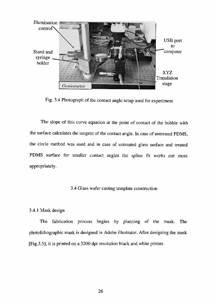
3.3.1 Photograph and description of the contact angle setup
Figure 3.4 shows a schematic of the contact angle setup used for the
experimental measurements in this treatise. The contact angle system is made of
the following blocks [24]:
• A CCD video camera with a resolution of 800-by-600 pixels;
• A XYZ axes translation stage capable of a minimum movement of l/50th
of a millimeter along each direction for mounting the camera;
• A ImL syringe with readable graduations of 0.0ImL for drop formation;
• Adjustable stand with provisions for holding the sample atop a
Goniometer, with a minimum tilt of 1/lOOth of a degree;
• A Syringe holder fixed permanently to the Adjustable stand holding the
syringe through alligator clips;
• A light source placed on a stand capable of moving vertically, with
adjustable levels of intensity and a light diffuser;
• The drop picture is captured on a video interface through a Computer
terminal and it analyzed by a software.
The contact angle is calculated using the image that is generated on the video
interface. An in-house developed software [24] is used to calculate the contact
angle wherein a matlab code is used to do a spline fit which is a quadratic
polynomial fit, a least square fit (based on fitment of data points on minimum
distances), and an equation of circle fit on points selected on the curve describing
the drop surface.
25
Illumination control
Stand and syringe holder
USB port to
computer
XYZ Translation
stage
Fig. 3.4 Photograph of the contact angle setup used for experiment
The slope of this curve equation at the point of contact of the bubble with
the surface calculates the tangent of the contact angle. In case of untreated PDMS,
the circle method was used and in case of untreated glass surface and treated
PDMS surface for smaller contact angles the spline fit works out more
appropriately.
3.4 Glass wafer casting template construction
3.4.1 Mask design
The fabrication process begins by planning of the mask. The
photolithographic mask is designed in Adobe illustrator. After designing the mask
[Fig.3.5], it is printed on a 3200 dpi resolution black and white printer.
26
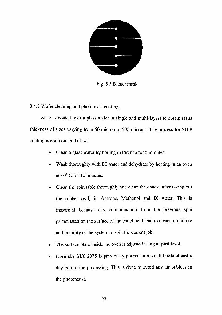
Fig. 3.5 Blister mask
3.4.2 Wafer cleaning and photoresist coating
SU-8 is coated over a glass wafer in single and multi-layers to obtain resist
thickness of sizes varying from 50 micron to 500 microns. The process for SU-8
coating is enumerated below.
• Clean a glass wafer by boiling in Piranha for 5 minutes.
• Wash thoroughly with DI water and dehydrate by heating in an oven
at 90° C for 10 minutes.
• Clean the spin table thoroughly and clean the chuck [after taking out
the rubber seal] in Acetone, Methanol and DI water. This is
important because any contamination from the previous spin
particulated on the surface of the chuck will lead to a vacuum failure
and inability of the system to spin the current job.
• The surface plate inside the oven is adjusted using a spirit level.
• Normally SU8 2075 is previously poured in a small bottle aUeast a
day before the processing. This is done to avoid any air bubbles in
the photoresist.
27
• A dummy glass wafer is used to set the spin speeds to the desired
level before any processing. (Table 3.2 mentions spin speeds.)
• The clean dehydrated wafer is set on the chuck.
• An adhesion promoter (AP 300) is poured on the surface of this
wafer and immediately spun at 1000 RPM for 10 seconds.
• Photoresist is poured over the wafer at the center in a big globule
form without any air inclusions in-between and spun.
• The wafer is taken to a preset oven without touching the top
photoresist layer and placed over the pre-aligned surface plate.
(Table 3.3 mentions temperatures and time.) Normally, for a 225
microns spun layer, the twin step heating is done at 65° C for 5
minutes followed by 95 ° C for 45 minutes.
• After pre-exposure bake, the wafer is cooled for 15 minutes inside
the litho room for removing the surface stickiness.
• For multi-layering, another coat of SU8 is given at this stage by
spinning another layer on the top of the baked SU8 layer. Note that,
if multi-layering is done without baking of the primary layer, the
effective thickness of photoresist remains same. By multi-layering,
the average thickness is approximately doubled.
• Expose the wafer in the UV exposure tool, keeping it upside down
on a silicon wafer. For a 450 micron, multi-layered wafer repeated
exposure of 15 seconds duration for 8 times proves to be adequate.
Normally all heating times. Pre and post exposure times and
28

developing times change with thickness of the resist and are found to
be a linear interpolation of the tabulated values for single layer.
The wafer is next subjected to a twin step post exposure baking
process (Table 3.4).
The post-baked wafers are put in SU8 nano-developer solution and
stirred. The developing should be done inside the litho room;
otherwise, the development is not proper due to exposure of wafer.
The approximate developing time for a 450-micron multi-layered
wafer is 15 minutes although it is better to keep checking the wafer
time and again.
Spraying isopropanol on the wafer after development can check the
residual undeveloped photoresist. If the wafer turns foggy and
whitish on spraying, it indicates residues of unexposed photoresist.
In this case the wafer requires more development.
The pattern size on the wafer obtained from the development stage
can be measured using calipers or screw gauge to check dimensional
consistency.
29
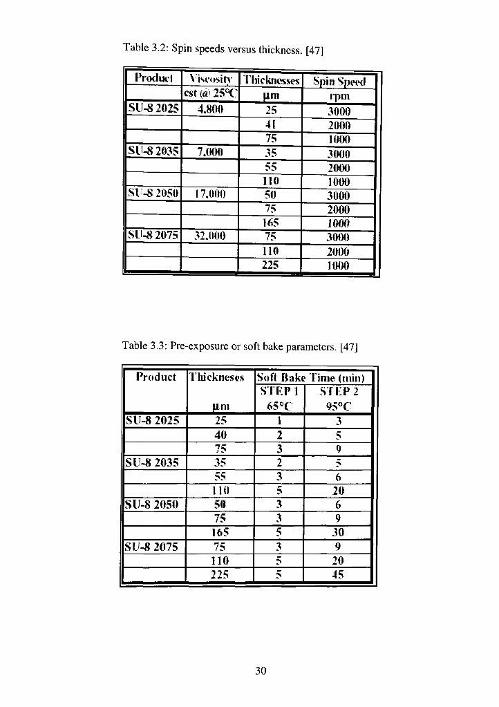
Table 3.2: Spin speeds versus thickness. [47]
Product
Sll-8 2025
Slf^ 2035
S l i^ 2050
SU^ 2075
\ IscositA est («) 25°C
4,800
7,000
17,000
32,0(M)
Thicknesses Um 25 41 75 35 55 110 50 75 165 75 110 225
Spin Speed ipni
3000 2W)0 1000 3000 2000 1000 3000 2000 1000 3000 2000 1000
Table 3.3: Pre-exposure or soft bake parameters. [47]
Product
SU-8 2025
SU-8 2035
SU-8 2050
SU-8 2075
1 hickneses
urn 25 40 75 35 55 110 50 75 165 75 110 225
Soft Bake Time (min) STEP 1
65°C 1 2 3 2 3 ^
3 3 5 3 5 5
STEP 2 95«C
3 5 9 5 6
20 6 9
30 9 20 45
30
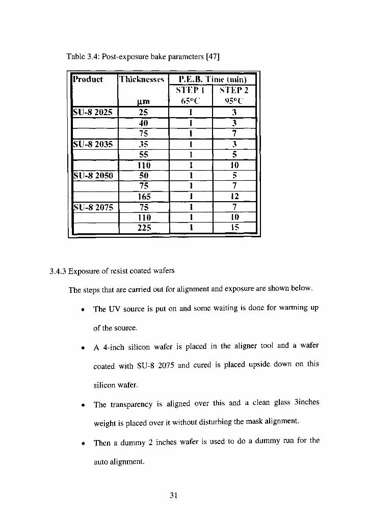
Table 3.4: Post-exposure bake parameters [47]
l^oduct
SU-8 2025
SU-8 2035
SU-8 2050
SU-8 2075
Thicknesses
UJm 25 40 75 35 55 no 50 75 165 75 no 225
P.E.B. Ii STEPl
65°C
1
me (min) STEP 2
y5°c 3 3 7 3 5 10 5 7 12 7 10 15
3.4.3 Exposure of resist coated wafers
The steps that are carried out for alignment and exposure are shown below.
• The UV source is put on and some waiting is done for warming up
of the source.
• A 4-inch silicon wafer is placed in the aligner tool and a wafer
coated with SU-8 2075 and cured is placed upside down on this
silicon wafer.
• The transparency is aligned over this and a clean glass 3inches
weight is placed over it without disturbing the mask alignment.
• Then a dummy 2 inches wafer is used to do a dummy run for the
auto alignment.
31
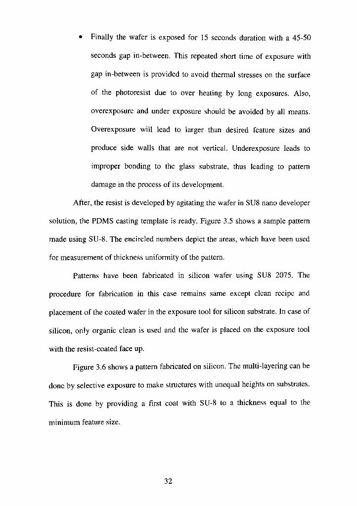
• Finally the wafer is exposed for 15 seconds duration with a 45-50
seconds gap in-between. This repeated short time of exposure with
gap in-between is provided to avoid thermal stresses on the surface
of the photoresist due to over heating by long exposures. Also,
overexposure and under exposure should be avoided by all means.
Overexposure will lead to larger than desired feature sizes and
produce side walls that are not vertical. Underexposure leads to
improper bonding to the glass substrate, thus leading to pattern
damage in the process of its development.
After, the resist is developed by agitating the wafer in SU8 nano developer
solution, the PDMS casting template is ready. Figure 3.5 shows a sample pattern
made using SU-8. The encircled numbers depict the areas, which have been used
for measurement of thickness uniformity of the pattern.
Patterns have been fabricated in silicon wafer using SU8 2075. The
procedure for fabrication in this case remains same except clean recipe and
placement of the coated wafer in the exposure tool for silicon substrate. In case of
silicon, only organic clean is used and the wafer is placed on the exposure tool
with the resist-coated face up.
Figure 3.6 shows a pattern fabricated on silicon. The multi-layering can be
done by selective exposure to make structures with unequal heights on substrates.
This is done by providing a first coat with SU-8 to a thickness equal to the
minimum feature size.
32
Fig. 3.6 SU-8 mold of thickness 450 microns using multi-layering and single exposure
Fig. 3.7 SU-8 fabricated on silicon with single layer, single exposure and resist thickness 150 microns.
33
This is followed by another coat, which is again selectively exposed such
that those areas, which are higher than the minimum feature size, are exposed.
This causes the exposed resist thickness to be greater at some selective
places. Figure 3.8 shows a side view and a photograph taken with a microscope,
for such a process, where the hatched channels are 150 microns and the chambers
are 300 micron thick. The masks for this process are shown in Figure 3.8.
300 microns 150 microns
\ 2zzaz3 \/j//j/)tA y " f " " f " ' ' \i>j>i////k
Figure 3.8 SU-8 structure of unequal height and its microscopic image fabricated with multi-layer and multi-exposure.
34
1 St Exposure 2nd Exposure
Figure 3.9 Masks for 1st and 2nd exposure
Table 3.5 Thickness measurements on the molds in Figures 3.5, 3.6, 3.7 and blister
Figure No.
Figure 3.5
Figure 3.6
Figure 3.7
Blister mold
Area Number
1
2
3 4 5 1 2 3 4 5 6 7 1 2 3 4 5 6 7 1 2 3 4 5
Actual thickness (microns)
450
450
450 450 450 150 150 150 150 150 150 150 300 300 300 300 150 150 150 150 150 150 150 150
Measured thickness (microns)
408.9
419.1
457.2 437.2 426.7 165.1 144.8 122 127 132.1 139.7 152.4 317.5 297.2 274.32 330.2 142.2 122 134.6 165.1 127 122 127 152.4
Deviation from actual (microns)
26.1
16.9
21.7
18.99
20.39
35
Table 3.5 shows a set of thickness measurements taken on the molds in
Figures 3.5, 3.6 and 3.7. The area numbers where the measurements are taken are
marked in the figure.
3.5 Fabrication of blister
3.5.1 PDMS molding
With the fabrication of the SU8 master on glass, the PDMS molding process
begins. The GE silicone kit is used to prepare the PDMS with a 10:1 ratio by
weight of monomer to the curing agent. After thorough stirring, the mixture is
placed in vacuum desiccator for 20-25 minutes at room temperature. This
degasses the PDMS and converts it into a completely transparent liquid. The SU8
mold is kept in a well-milled aluminum plate mounted on a tripod [Figure 3.9]
and the liquid PDMS is poured over it. Normally, a slow pouring rate is desirable
to avoid bubble formation. The plate is next leveled inside the convection oven
pre set to 80°C.
The PDMS heat cures in 45 minutes. The plate is then taken out and PDMS
stamp is slowly separated from the master. The PDMS stamps are thicker on the
outer due to the edge effects. The edges are removed carefully by using a circular
cutter or an axacto knife. Next, a rectangular shape is cut around the blister.
Cleanliness of the PDMS stamp is vital to its good bonding to glass and PDMS
substrates. Normally, the PDMS pieces are enclosed in a clean petri dish to keep it
safe from contamination.
36
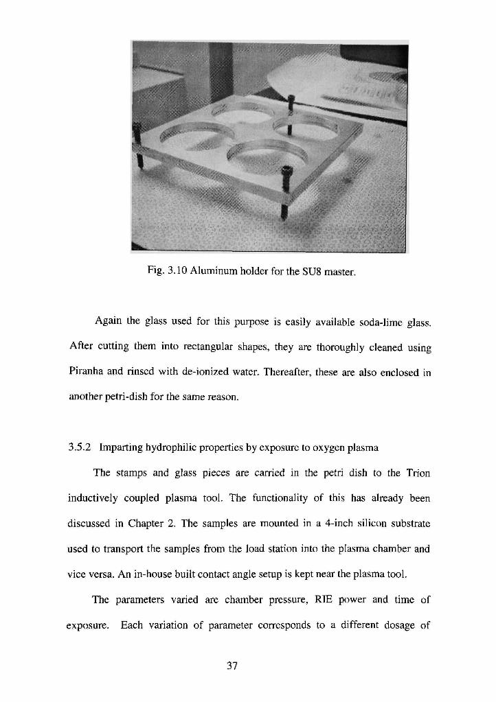
Fig. 3.10 Aluminum holder for the SU8 master.
Again the glass used for this purpose is easily available soda-lime glass.
After cutting them into rectangular shapes, they are thoroughly cleaned using
Piranha and rinsed with de-ionized water. Thereafter, these are also enclosed in
another petri-dish for the same reason.
3.5.2 Imparting hydrophilic properties by exposure to oxygen plasma
The stamps and glass pieces are carried in the petri dish to the Trion
inductively coupled plasma tool. The functionality of this has already been
discussed in Chapter 2. The samples are mounted in a 4-inch silicon substrate
used to transport the samples from the load station into the plasma chamber and
vice versa. An in-house built contact angle setup is kept near the plasma tool.
The parameters varied are chamber pressure, RIE power and time of
exposure. Each variation of parameter corresponds to a different dosage of
37
exposure. After each run, two pieces of the exposed replica molded PDMS
samples are brought into conformal contact resulting in irreversible covalent
bonding instantly. The third piece is immediately used for measuring the contact
angle by sessile drop method to gauge the hydrophilicity level of the surface.
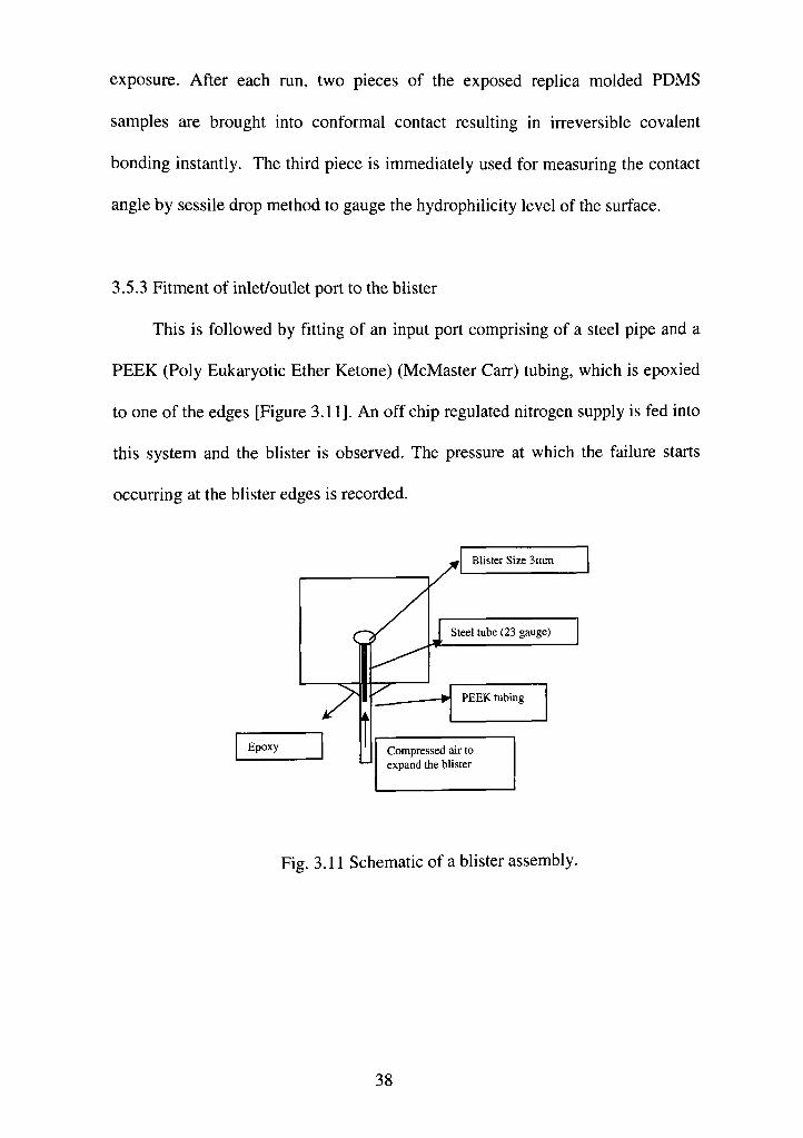
3.5.3 Fitment of inlet/outlet port to the blister
This is followed by fitting of an input port comprising of a steel pipe and a
PEEK (Poly Eukaryotic Ether Ketone) (McMaster Carr) tubing, which is epoxied
to one of the edges [Figure 3.11]. An off chip regulated nitrogen supply is fed into
this system and the blister is observed. The pressure at which the failure starts
occurring at the blister edges is recorded.
Blister Size 3mm
Epoxy
Steel tube (23 gauge)
PEEK tubing
Compressed air to expand the blister
Fig. 3.11 Schematic of a blister assembly.
38
CHAPTER 4
RESULTS, DISCUSSION, AND CONCLUSION
4.1 Introduction
Testing is primarily done for two aspects. One is the surface roughness
wherein the two replica molded PDMS pieces are casted on a roughened surface
and bonded to each other or to another roughened surface of soda-lime glass. The
second aspect covers variation of chamber parameters and evaluation of bond
strength and contact angle.
The testing is primarily done over a range of different rough nesses
varying from 1 micron to 30 micron respectively in the first set of experiments.
The second set of testing is done by varying the chamber pressure, reactive ion
etching power, and exposure time, one by one and keeping the inductively
coupled power and the gas flow rate constant.
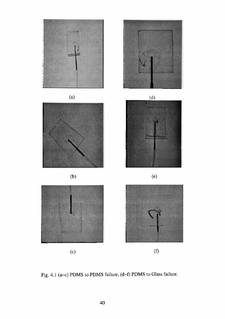
The fabricated blister in section 3.5.3 is tested using compressed nitrogen
and the pressure at which the layers start separating is noted down as a measure of
the bond strength. This procedure is a standard test, which was first reported in
1961 by Dannenberg [49] and is more recentiy used to measure the adhesion
between polymer layers [50, 51] thin films, etc. [52]. Figure 4.1(a~f) shows
pictures of the blisters after failure. As can be seen in most of the cases the failure
occurs due to the separation of layers at the interface. However, the pressure value
is noted at the start of failure process.
39
(a)
(b) (e)
(c) (f)
Fig. 4.1 (a~c) PDMS to PDMS failure, (d~f) PDMS to Glass failure.
40
This chapter draws two interesting correlations between:
1. Bond strength and surface roughness.
2. Bond strength and surface hydrophilicity gauged by measure of
contact angle.
The trend obtained is further explained by considering how the various
dosages of plasma and various surface roughness values affect the bond strength.
4.2 Surface roughness versus bond strength
The glass wafers are lapped over wet diamond laps of various dimensions
ranging from 1 micron to 30 micron.
4.2.1 Lapping process
Lapping is a material cutting process similar to the five major machining
processes of milling, drilling, grinding, turning, and shaping. Lapping is
considered a sub-category of the major machining operation of grinding. All of
these processes are used to cut chips from various materials or in the case of
amorphous materials such as ceramic and glass, micro-fracture and abrade the
material [53]. Lapping cuts microscopic chips with a very low stock removal rate
as compared to milling which cuts large chips and removes a high volume of
stock in a single pass. This is why lapping and polishing are considered micro-
machining processes. Lapping process techniques are very diverse and material
specific as opposed to the other machining operations which are much more
quantitative and have fewer process variables (traverse speed, RPM of tool or
41
component and depth of tool cut). Many consider lapping to be a machining art in
comparison to other machining sciences.
A surface that has been lapped exhibits a dull, non-reflective and multi
directional appearance. This condition is referred to as "matte" finish. There may
be slight reflectivity on materials lapped with very small micron size aluminum
oxide abrasive. This is especially true if the material is relatively hard and the
surface roughness measurement is perhaps 5 micro-inch (.127 micron) [53] and
below.
Very light "micro-scratches" may be viewed on lapped surfaces. Abrasive
of larger micron size and harder compound will generate more micro-scratches in
addition to deeper scratches. Most micro-scratches produced with small micron
aluminum oxide abrasive will be less than .025 micron deep [54] and cannot
usually be measured with a profilo-meter. Micro-scratches should not be confused
with deeper scratches produced by particles of contamination or other causes.
Typically lapping rates are very low to begin with (usually less than 2.54 micron
per minute) [54].
Although the lapping operation in general results in very rough and non
reflective surfaces still in some cases certain materials can be lapped to an
extremely flat condition and polished to a reflective finish in one step. This can be
accomplished using diamond super-abrasive particles in conjunction with a
variety of special and standard lapping plates.
Due to the exceptional cutting ability of diamond compounds on different
ranges of materials, diamond lapping is becoming more popular in the ceramic
42
and metalworking industry [54]. Diamond compounds, originally developed for
finishing of tungsten carbide cutting tools, have proven to be economical for
lapping hard materials.
4.2.2 Roughness measurement
The surface roughness of the lapped wafers is measured using NT 1100
interferometer. The NTl 100 provides high-resolution 3D surface measurement,
from sub-nanometer roughness to millimeter-high steps. The NTl 100 WYKO
optical system analyzes all data with Vision 32 analytical software package.
Advanced optics ensure sub-nanometer vertical resolution at all magnifications.
The Data Stitching option adds a motorized stage for high-resolution
measurements over a larger field of view. The NTl 100 enables accurate, cost-
effective metrology for R&D and production of MEMS, thick films, optics,
ceramics, and advanced materials.
The glass specimen is set on the interferometer table and a 1 micron area
is scanned on its surface. The objective lens is focused to a distance from the
specimen where the fringes are clearly visible. The Vision 32 is used at this point
to give an average roughness value of the surface being scanned. Table 4.1 shows
the various roughness parameters obtained from scanning the surface.
For the purpose of measurement of surface roughness of the lapped glass
wafers, the Rz value is the most appropriate one. This may be because as, this
parameter measures the 10 highest and 10 lowest points in one scan, thus it comes
closest to the micro-scratch level induced by lapping operation.
43
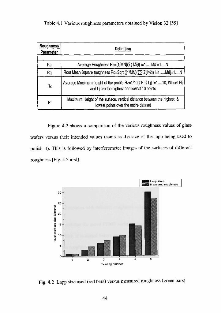
Table 4.1 Various roughness parameters obtained by Vision 32 [55]
Rouqhness
Parameter
Ra
Rq
Rz
Rt
Definition
Average Roughness Ra=(1/MN)(ZIIZijl) i=1 M&i=1....N
Root Mean Square roughness Rq=Sqrt.((1/MN)(ZXIZijl'^2)) i=1 M&j=1....N
Average Maximum height of the profile Rz=1/10(XHj-XLj) j=1 ....10, Where Hj
and Lj are the highest and lowest 10 points
Maximum Height of the surface, vertical distance between the highest &
lowest points over the entire dataset
Figure 4.2 shows a comparison of the various roughness values of glass
wafers versus their intended values (same as the size of the lapp being used to
polish it). This is followed by interferometer images of the surfaces of different
roughness [Fig. 4.3 a~d].
3 4
Reading number
Fig. 4.2 Lapp size used (red bars) versus measured roughness (green bars)
44
'W''' ''at^^J^^^
(a) 30 microns (b) 15 microns
j^WP%s,^|(t
(c) 9 micron (d) 6 microns
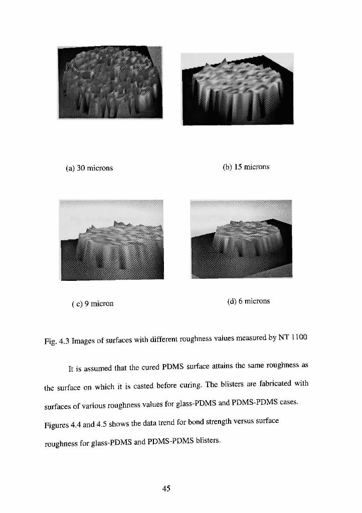
Fig. 4.3 Images of surfaces with different roughness values measured by NT 1100
It is assumed that the cured PDMS surface attains the same roughness as
the surface on which it is casted before curing. The blisters are fabricated with
surfaces of various roughness values for glass-PDMS and PDMS-PDMS cases.
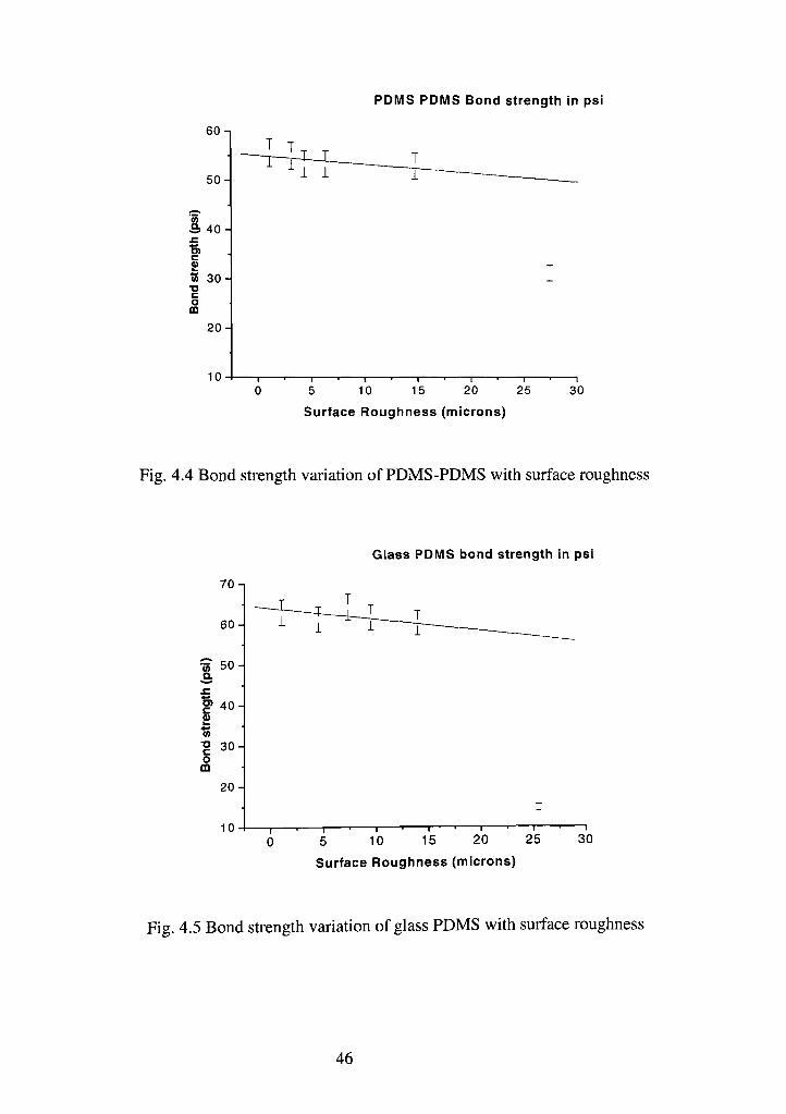
Figures 4.4 and 4.5 shows the data trend for bond strength versus surface
roughness for glass-PDMS and PDMS-PDMS blisters.
45
PDMS POMS Bond strength in psi
60 n
50-
S 40 £ B)
to 30-•a c o m
20-
10 — I —
15 — I ' 1 —
20 25 0 5 10
Surface Roughness (microns)
30
Fig. 4.4 Bond strength variation of PDMS-PDMS with surface roughness
70-
6 0 -
•<5 Q. ^•^ £
ngt
t>
at •a c o m
50
40
30
20-
10
Glass PDMS bond strength in psi
-• r-5 0 5 10 15 20
Surface Roughness (microns)
— I ' 1
25 30
Fig. 4.5 Bond strength variation of glass PDMS with surface roughness
46
The PDMS-PDMS bond strength starts from a maximum of 55 psi and
remains within +/- 5 psi uptill 15 micron surface roughness which is the
experimental error range for bond strength. As surface roughness increases further
there is a fall in the bond strength to 32 psi at 26 microns roughness. The glass
PDMS bond has a maximum strength in the range of 65- 70 psi. As can be seen
there is a substantial fall in bond strength over 26 microns surface roughness in
case of glass-PDMS bond. This fall is much larger than its predecessor. The bond
strength value at this pressure is 14 psi.
This behavior can be explained by considering the interface before
bonding. As the surface of PDMS is extremely flexible, the surfaces conform to
the shape of each other and thus fill out all cavities between them. This way they
can come in very close proximity and thus higher bond strength is inevitable. [Fig.
4.6 (a)] In the glass PDMS case only one of the surfaces is flexible. Thus only the
PDMS surface conforms to the cavities in glass. As the glass surface is rigid thus
in this case the proximity is not as close as in the earlier case [Figure 4.6 (b)].
This results in reduced bond strength at higher roughnesses.
Higher gap
between surfaces
(b)
Fig 4.6 Schematic of PDMS-PDMS and Glass PDMS interface
47
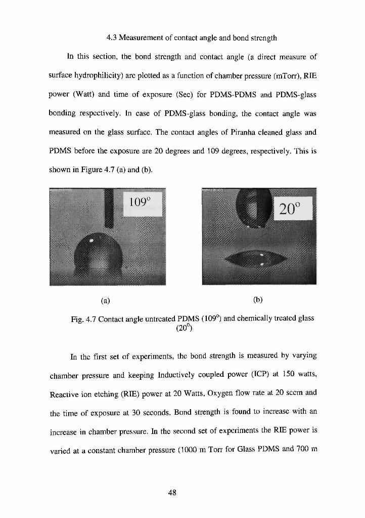
4.3 Measurement of contact angle and bond strength
In this section, the bond strength and contact angle (a direct measure of
surface hydrophilicity) are plotted as a function of chamber pressure (mTorr), RIE
power (Watt) and time of exposure (Sec) for PDMS-PDMS and PDMS-glass
bonding respectively. In case of PDMS-glass bonding, the contact angle was
measured on the glass surface. The contact angles of Piranha cleaned glass and
PDMS before the exposure are 20 degrees and 109 degrees, respectively. This is
shown in Figure 4.7 (a) and (b).
(a) (b)
Fig. 4.7 Contact angle untreated PDMS (109°) and chemically treated glass (20°)
In the first set of experiments, the bond strength is measured by varying
chamber pressure and keeping Inductively coupled power (ICP) at 150 watts,
Reactive ion etching (RIE) power at 20 Watts, Oxygen flow rate at 20 seem and
the time of exposure at 30 seconds. Bond strength is found to increase with an
increase in chamber pressure. In the second set of experiments the RIE power is
varied at a constant chamber pressure (1000 m Torr for Glass PDMS and 700 m
48
Torr for PDMS-PDMS) and all other parameters same as before. In the third
experiment the time of exposure is varied and remaining parameters kept same as
before. The variation in RIE power and time of exposure indicates maximum
bond strength at a certain optimum value of power and time. This observation is
true for both PDMS to PDMS and PDMS to glass bonding. A theoretical
calculation of bond strength has been made for PDMS/PDMS in Appendix B
using Maxwell's equation. The following subsections of this chapter describe
these effects in details.
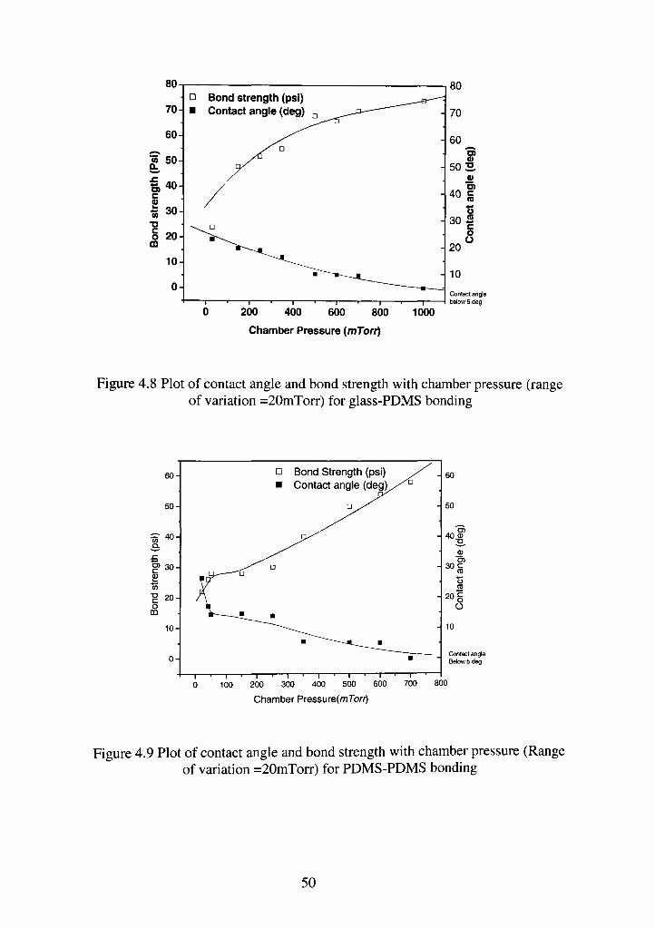
4.3.1 Effect of chamber pressure variation
Figures 4.8 and 4.9 illustrate plots for contact angle and bond strength
versus chamber pressure for a fixed RIE power and exposure time for glass-
PDMS and PDMS-PDMS bonding respectively. Bond strength is measured as the
value of pressure at which interfacial separation of the pressurized blister starts
occurring. The maximum bond strength obtained for glass to PDMS bond is 72-
psi. This corresponds to a contact angle of less than 5 degrees.
There is a decrease in bond strength below 100 mTorr pressures. Normally,
at a chamber pressure of 100 mTorr or less the plasma etching becomes highly
directional and anisotropic [19]. The high level of anisotropy in etching leads to a
damage in the siloxane backbone instead of etching the surface methyl groups.
The change in contact angle measured on the glass surface does not show a
sporadic decrease like that of PDMS for reason explained later. For PDMS-PDMS
bonding, the maximum bond strength is found to be 58 psi. The corresponding
49
80
70-
60-
50-
40-
30
20
10
• Bond strength (psi) • Contact angle (deg) ^
200 400 600 800
Chamber Pressure (mTori)
1000
Figure 4.8 Plot of contact angle and bond strength with chamber pressure (range of variation =20mTorr) for glass-PDMS bonding
60-
50-
40'
g> soil) to •g 20-o m
10-
Bond Strength (psi) Contact angle (deg)
— I — 100 200
— I — 300
— I — 400
— I — 500
— I — 600
— I — 700
Chamber Pressure{mTorr)
60
50
O) 40 0)
O) 30 5
Co
20 g O
10
Contact angle Below 5 deg
800
Figure 4.9 Plot of contact angle and bond strength with chamber pressure (Range of variation =20mTorr) for PDMS-PDMS bonding
50
contact angle is found to be less than 5 degrees. The bond strength curve in the
low pressure region(<100 mTorr) is similar to the curve for glass to PDMS
bonding. In the high-pressure region (>100mTorr) there is a gradual increase in
the bond strength and decrease in contact angle with an increase in pressure. The
behavior of the data in the high-pressure region can be explained in the following
way. As the chamber pressure increases the mean free path of the gas molecules
reduce, and the plasma becomes more and more isotropic. This homogeneity
drives the plasma to act uniformly over the substrate. Also with an increase in
pressure the sheath of charged particles formed near the electrode move closer to
the substrate [19]. So, newly formed ions near this sheath have smaller distances
to travel before striking on to the substrate resulting in less momentum transfer.
Less energetic oxygen ions generated in this way remove methyl groups from the
surface without damaging the material.
One more important behavior of the trend is reflected at pressures below
100 mTorr where the contact angle of PDMS rises faster than that of glass. This
can be explained by considering, that glass is more rigid structurally. So at a low
pressure and greater mean free paths when the ionic momentum transfer increases
it is sufficient to damage the fiexible siloxane backbone in PDMS but not
sufficiently strong to affect the sturdy surface structure of glass. Thus the contact
angle in the case of glass does not increase so much at lower pressures as in case
of PDMS. The behavior of the bond strength is by and large reverse to that of
contact angle, which fits our theory very well. However, the point corresponding
to the pressure value of 50 mTorr [Figure 4.9] shows a sudden reduction in the
51

bond strength value which may indicate an extraordinary damaging of the PDMS
structure and thus a substantial loss of surface silanol bond density. Thus, in this
case although the alteration of glass surface is relatively less but the damage to
PDMS surface causes a huge decrease in bond strength. All measurements have
been taken for a constant value of PDMS substrate thickness (2.5 mm) although
the effect of changing thickness can be estimated. If thickness of the substrate is
reduced, then at lower pressures, the ionic sheath near the electrodes is nearer to
the substrate surface causing the ions to hit the surface with less impact than in
the case of thinner substrate. Thus, the surface damage at lower pressure is lesser
for thicker samples and the bond strength value should rise up slightly at lower
pressure. However, at higher pressure, there may be a possibility of the surface
rising above the dark space and thus facing negligible plasma activity. So thick
ness cannot be abruptly increased
4.3.2 Effect of RIE power variation
Figures 4.10 and 4.11 show plots of contact angle and bond strength for
variation of RIE power. The data shows an interesting trend wherein the bond
strength peaks at 20-watt RIE power for glass to PDMS and PDMS to PDMS
bonds. The peak value of bond strength here in both cases are similar to those
obtained before, with 68 psi for PDMS-Glass and 54 psi for PDMS-PDMS. The
contact angle trend follows an inverse behavior to bond strength. The contact
angle curve dips down to below 5 degrees at 20 watt RIE power level and then
52
70-
60-
^ 50-'</) a.
£ 40-OJ c 2 30-w
• D
§ 20-m
10-
0-
0
g
1* •
' 1
20
• Contact Angle (deg) D Bond strength (psi)
^°~~~~~----.c
• ^ ^ - ^ m^-^^
• ^
40 60 80 100 120
RIE Power (Watt)
~~~~~---5
• ,
140
-
_
.
-
160
70
60
50 S •D " • " ^
O 40 'i
CS
30 iS c o o
20
10
Contact angle below 5 deg
Figure 4.10 Plot of contact angle and bond strength with RIE power( range of variation= 2W) for glass-PDMS bonding
60-
50-
in n .c
c (i>
r« T3 c o m
40
30
2U
10-
0-
- l — ' — I — I — I — ' - I — I — I — ' — I — • — I — ' -
- Bond strength (psi) Contact angle (deg)
60
50
1-40 §>
<i>
1-30 o)
20 I c o
h i o "
Contact angle Below 5 deg
0 20 40 60 80 100 120 140 160
RIE power (W)
Figure 4.11 Plot of contact angle and bond strength with RIE power (Range of variation=2W) for PDMS-PDMS bonding
53
goes up on either side of this value. Simultaneously, the bond strength goes down
as the contact angle goes up.
This behavior can be explained by considering the plasma behavior for
various bias levels dictated by RIE power. At low power levels, the kinetic energy
of ions incident on the substrate reduces. This coupled with the ambient high
chamber pressure leads to a large reduction in the number of reactive ions on the
substrate. This is so because a lower power level reduces the electron acceleration
within the plasma environment thus leading to a reduction in the radical density.
Thus less number of active sites formulate on the substrate surface after
etching in such a plasma environment, which leads to a reduction in surface
bondage. The ions tend to thus graze on the surface of the substrate without
producing much chemical or physical change of the surface. The reverse
behavior at higher power levels suggests an increase in the ion bombardment.
Thus the Si-O-Si, whose dissociation energy (445KJ/mol) is much higher
than the Si-C bond dissociation energy (306KJ/mol.), is affected resulting in
damage of the overall uniquely fiexible Siloxane backbone [19].
Contrary to the chamber pressure variation case, one important observation
in this trend is a general homogeneity in variation of the contact angle and bond
strength in both glass-PDMS and PDMS-PDMS bonds. This can be attributed to
the constancy in the chamber pressure due to which directionality never arises in
the etching. This helps in preventing the differential nature of trends in both cases
by eliminating the anisotropicity levels as had happened in the low chamber
pressure case.
54
4.3.3 Effect of time of exposure
The time of exposure has a similar trend as RIE power [Figure 4.8(a) & (b)].
The bond strength peaks in this case for an exposure time of 20 sees. The values
of strengths are similar to that obtained in the earlier cases with a rise in contact
angle and subsequent fall in bond strength at a longer or shorter exposure time.
The least contact angle value at highest bond strength is again less than 5 degrees.
One possible explanation can be obtained from Owen and Smith's [56]
investigation on the PDMS surface after high RF power and longer treatment.
The progressive oxidation of the surface leads to the formation of an
extremely brittle silica layer on the surface. Owen and Smith have clearly seen
cracking on the surface under scanning electron microscope (SEM). They
mentioned that less harsh, lower RF power, and shorter treatment times produced
un-cracked surfaces with a layer of Silica [SiOx], which retards the migration of
low molar mass molecules from the bulk of the structure [Fig. 4. 12 and 4.13]. As
this layer is exposed longer in a plasma environment this layer cracks and
promotes transport of low molar mass molecules to the surface, which covers the
oxidized layer. Another possible explanation of this trend can be obtained from
the work of Hillborg and Gedde [57] who suggest that prolonged UV exposure in
a plasma environment makes the surface undergo fast hydrophobic recovery.
They have mentioned about the various transformations, which take place on
prolonged UV exposure [Figure 4.12 and 4.13]. The longer exposures to oxygen
plasma and UV of a treated PDMS surface results in the formation of excessive
surface silanol concentration [58].
55
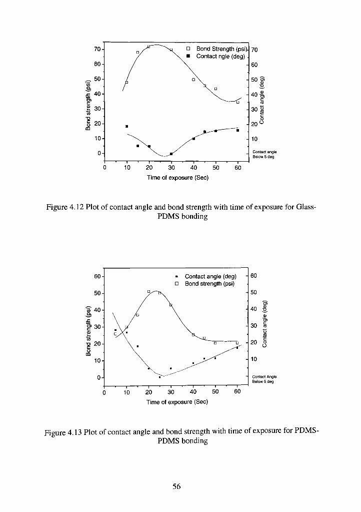
70-
60
50 Q.
40
i 30-tn
T3 g 20
CD
10-
0-— I —
10
a Bond Strength (psi). Contact ngle (deg)
— I — 40 20 30 40 50
Time of exposure (Sec)
60
70
60
50 o>
40 ra
30
- 20
10
Contact angle Below 5 deg
Figure 4.12 Plot of contact angle and bond strength with time of exposure for Glass-PDMS bonding
60-
50-
•tf)
a. ,c r a> (0
T3 c o m
40
30
?0
10-
• Contact angle (deg) D Bond strength (psi)
- 60
—1 1 1 1 1 1 I ' I
10 20 30 40 50
Time of exposure (Sec)
60
- | Contact Angle Below 5 deg
Figure 4.13 Plot of contact angle and bond strength with time of exposure for PDMS-PDMS bonding
56
As the silanol bond density increases it results in chemical transformation on the
surface known as polymer surface chain scission reactions. In such a situation a
marked reduction in the number of surface silanol bonds occur by back biting
scission reactions [Figure 4.17, la] and a physical surface cracking and a gradual
migration of the mobile, low molar mass PDMS oligomers to the surface [Figure
4.14 and 4.15] [56]. If chemical transformation takes place by scheme 2 and 3 as
shown in Figure 4.16 the scission reactions occur in a variety of ways like [Figure
4.17,1b, n, and III].
In all cases due to a rearrangement of the surface molecules in short and
long cyclical chains, the surfaces get cracked and damaged at several places
which promotes surfacing out of the low molecular mass oligomers and thus a
reduction in the hydrophilicity [58].
A general trend was plotted using all values of contact angle and bond
strength for all different plasma parameters [Figure 4.18 and 4.19]. The plot gives
a universal increase in bond strength with decrease in contact angle for both glass-
PDMS and PDMS-PDMS cases for variation of RIE power and pressure. The
time of exposure if plotted doesn't follow this universal trend on the longer
exposure side. Although the bond strength reduces with increase in contact angle
for longer exposures but still the slopes of the graph on both sides of the optimum
time are dissimilar. This is true for both glass-PDMS and PDMS-PDMS bonding.
Thus it is clear that the trend shown by the universal curve works till and until the
surface is not damaged severely causing the cracking of the surface. There is a
relatively large spread in the data points in case of glass/ PDMS bonding. This
57
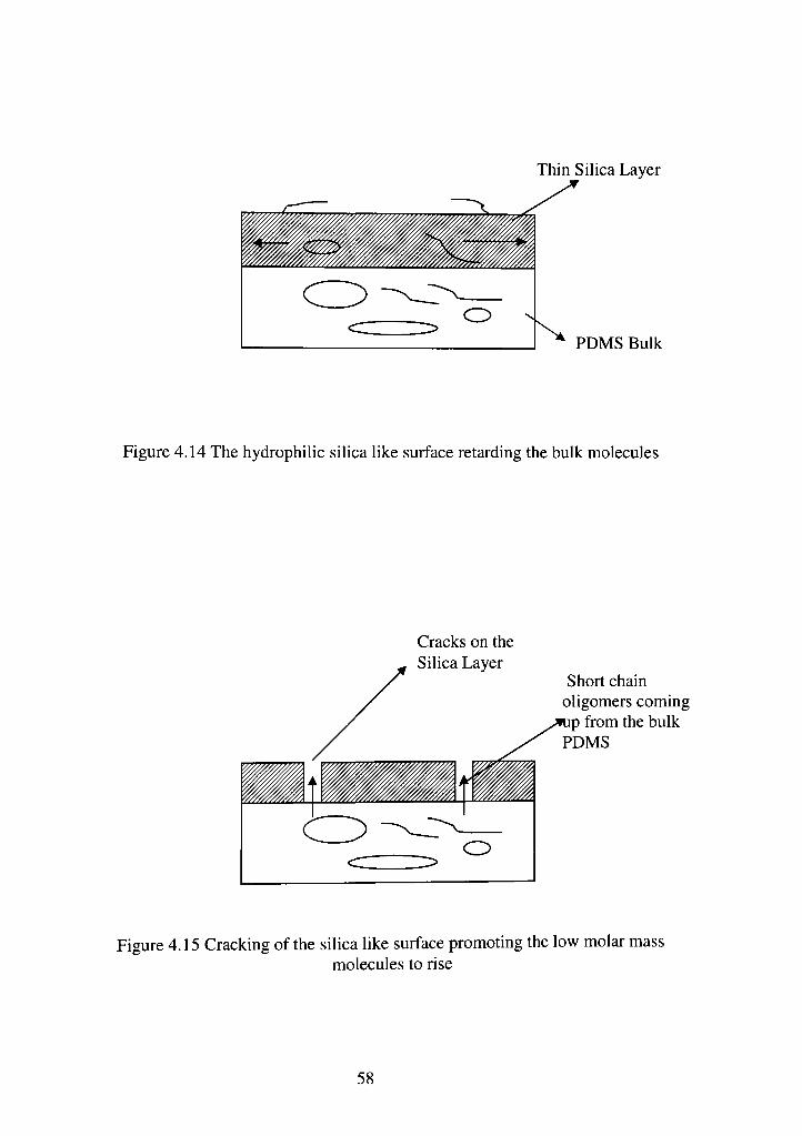
Thin Silica Layer
PDMS Bulk
Figure 4.14 The hydrophilic silica like surface retarding the bulk molecules
Cracks on the Silica Layer
Short chain oligomers coming p from the bulk
PDMS
Figure 4.15 Cracking of the silica like surface promoting the low molar mass molecules to rise
58
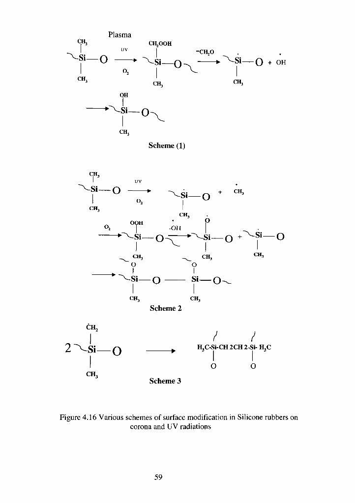
Plasma
UV ^fl' CHjOOH
v.si_o • ~vsi_o-^ •^s i—o + OH I o, I V I
CH, ' ' CH, CH,
CH,
Scheme (1)
CHj I UV
" ^ S i O • -^ + CH
OOH -OH
Q
CH3 ^ CH3
o o
^ • ^ S i — o S i — o
CH3
Scheme 2
CEL
I / / 2 ^ S i O • HjC-Si-CH 2CH 2-Si- H3C
I o o CH3
Scheme 3
Figure 4.16 Various schemes of surface modification in Silicone rubbers on corona and UV radiations
59
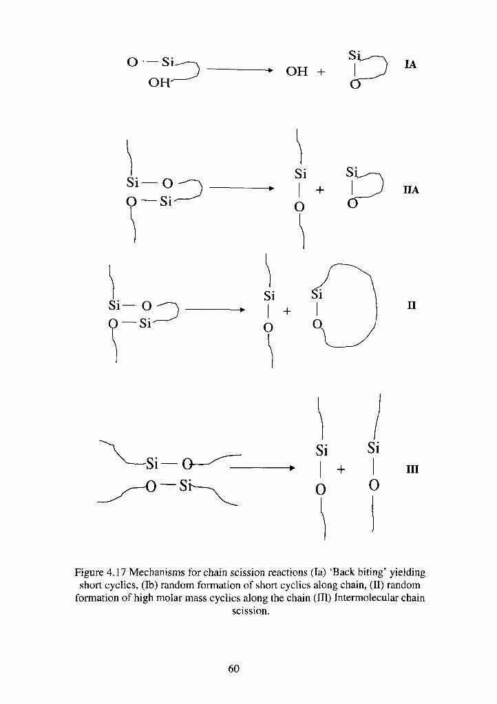
O — Si
OH -• O H +
lA
IIA
II
Si
0 +
Si
0 III
Figure 4.17 Mechanisms for chain scission reactions (la) 'Back biting' yielding short cyclics, (lb) random formation of short cyclics along chain, (II) random
formation of high molar mass cyclics along the chain (III) Intermolecular chain scission.
60
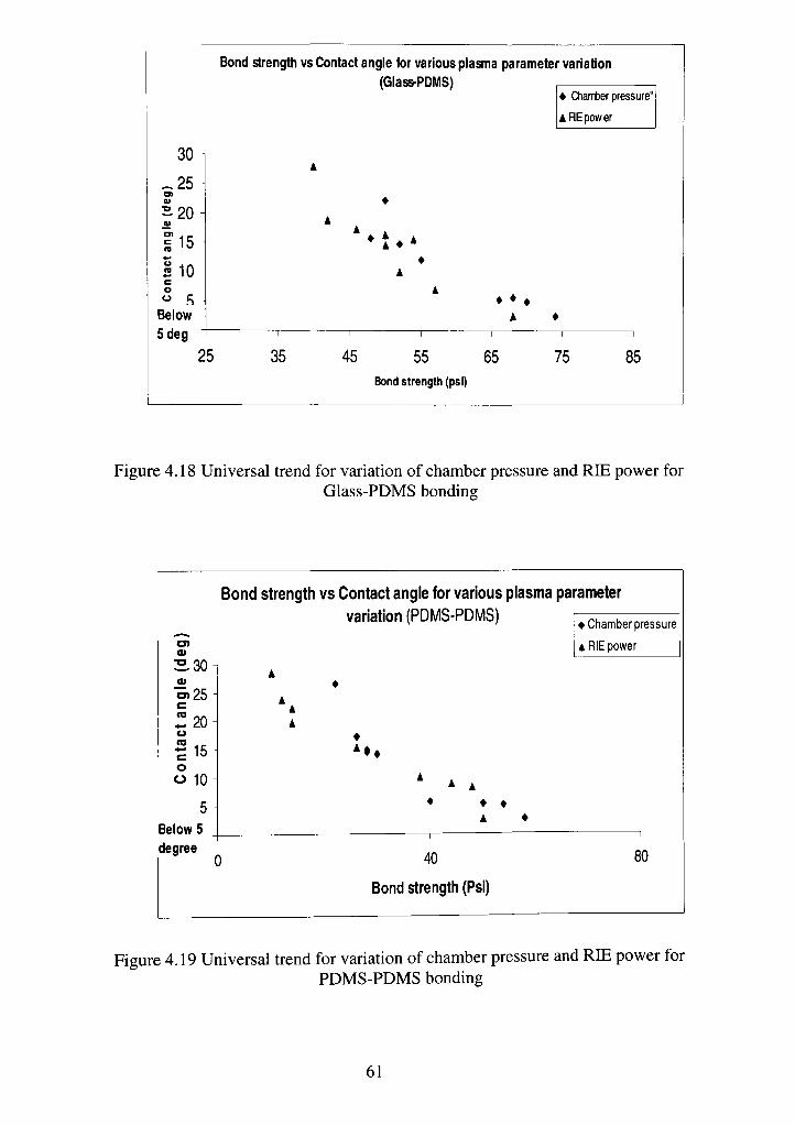
Bond strength vs Contact angle for various plasma parameter variation (Glass-PDMS)
30 1
^25
S20-
!15
l i o c o
Below
I
• Chanter pressure"
A RE power
•
A •
5 deg i i i i i i
25 35 45 55 65 75 85
Bond strength (psi)
Figure 4.18 Universal trend for variation of chamber pressure and RIE power for Glass-PDMS bonding
Bond strength vs Contact angle for various plasma parameter
variation (PDMS-PDMS)
330 <u "5)25 1=
:!2o o •0 , _ - l b o o 10
5 Below 5 degree
• Chamber pressure
A RIE power
•
A A
• • • A •
40
Bond strength (Psi)
80
Figure 4.19 Universal trend for variation of chamber pressure and RIE power for PDMS-PDMS bonding
61
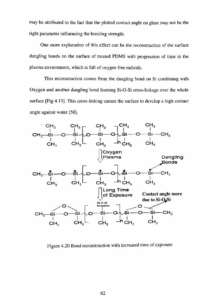
may be attributed to the fact that the plotted contact angle on glass may not be the
right parameter influencing the bonding strength.
One more explanation of this effect can be the reconstruction of the surface
dangling bonds on the surface of treated PDMS with progression of time in the
plasma environment, which is full of oxygen free radicals.
This reconstruction comes from the dangling bond on Si combining with
Oxygen and another dangling bond forming Si-O-Si cross-linkage over the whole
surface [Fig 4.13]. This cross-linking causes the surface to develop a high contact
angle against water [58].
CH,
CH^-—SI O-
CHn
CH3—Si-I
CH.
CH,
CH,
CH3 —
CH,
^ CH,
CH, CH,
v.,0 Si O^v-Si——O Si-
CH, CH-!
V
Oxygen Plasma
I CH, CH, CH,
-CH,
Dangling onds
^ i ^ ^^JO—SI O v ^ i O Si CH
\7
Long Time of Exposure Contact angle more
due to Si-OsSi
Figure 4.20 Bond reconstruction with increased time of exposure
62
Depending on the plasma properties, the surface that influences the bond strength
could be glass, PDMS or both.
Another important observation is the loss in the hydrophilicity when the
surface is kept outside after exposure to oxygen plasma. This can be attributed to
the reconstruction of the dangling bonds by molecular oxygen [58] and various
organic contaminants present in the atmosphere after placing the exposed surfaces
in open air.
63
CHAPTER 5
DESIGN CONSIDERATIONS FOR A MICRO REACTOR
5.1 Introduction
As mentioned in Chapter 1 the field of micro-fluidics has diverse
applications in chemistry and life sciences. Some examples of applications
include: measurement of the reaction gradient, screening of chemicals for drug
discovery or DNA synthesis, enzyme and substrate reactions and high
temperature and light induced reactions [1]. The advantages of moving to the
micro-scale are seen in terms of cleaner reactions due to frequent flushing out of
products, a very homogeneous temperature distribution for endothermic reactions,
higher safety levels particularly in case of hazardous reactions by reduction in the
volumes, and increased sensitivity [60]. In most of the chemical and biomedical
analysis, a sample solution is to be tested with a reagent [61]. Two or more than
two solutions are to be mixed, to make such reactions physically possible. Most of
the macro-scale mixers utilize the features of turbulent flow (fluctuating and
agitated) causing the formation of eddies and vortices across a large range of
length scale [62]. Mixing on the micro-scale relies mostiy on inter diffusion of
various species participating in the mixing process. This is due to the laminar
nature (smooth and steady) of flows at the micro-scale.
Although the flow behavior of fluids has been widely studied both
mathematically and physically, still no general analysis of fluid motions exist
[63]. The reason for this is that there is a profound and vexing change in fluid
behavior at moderate Reynolds number, which, is the ratio between the viscous
64
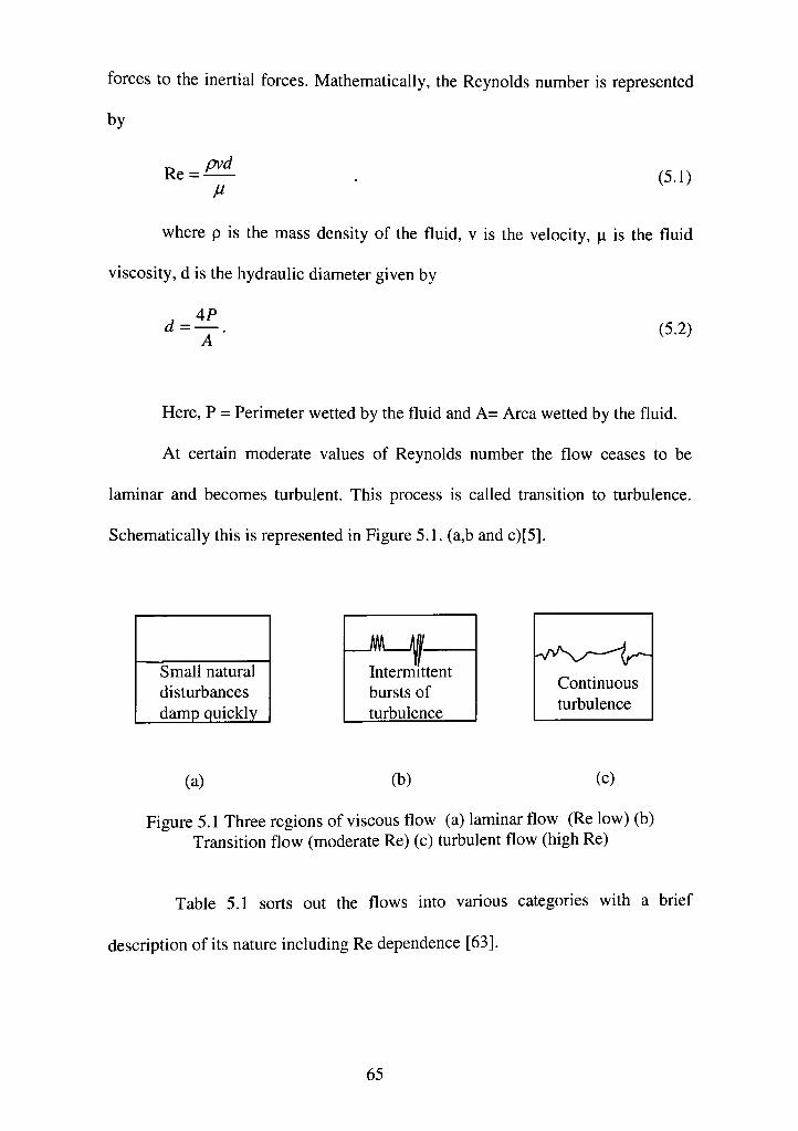
forces to the inertial forces. Mathematically, the Reynolds number is represented
by
Re = pvd
(5.1)
where p is the mass density of the fluid, v is the velocity, p is the fluid
viscosity, d is the hydraulic diameter given by
A (5.2)
Here, P = Perimeter wetted by the fluid and A= Area wetted by the fluid.
At certain moderate values of Reynolds number the flow ceases to be
laminar and becomes turbulent. This process is called transition to turbulence.
Schematically this is represented in Figure 5.1. (a,b and c)[5].
Small natural disturbances damp quickly
_JWL ^ -
Intermittent bursts of turbulence
Continuous turbulence
(a) (b) (c)
Figure 5.1 Three regions of viscous flow (a) laminar flow (Re low) (b) Transition flow (moderate Re) (c) turbulent flow (high Re)
Table 5.1 sorts out the flows into various categories with a brief
description of its nature including Re dependence [63].
65
Table 5.1 Ranges of 'Re' values and characterization of the nature of flow
S.No.
1
2
3
4
5
6
Range of 'Re'
0<Re<l
l<Re<100
100<Re<10^
1000<Re<10^
10VRe<10*'
10VRe<oo
Description
Highly Viscous, laminar "creeping motion"
Laminar, Strong Reynolds Number dependence
Laminar, Boundary layer theory is useful
Transition to turbulence
Turbulent, Moderate Reynolds Number dependence
Turbulent, Slight Reynolds Number dependence
Micro-scale mixing rates strongly depend on the flux of diffusion O
mathematically expressed by
ax (5.3)[63]
where D is the diffusion coefficient in m^ / sec and c is the species
concentration in kg/ m l The diffusion coefficient is inversely proportional to the
fluid viscosity at a constant temperature.
Figure 5.2 [4] represents a range of coefficient for various states of
matter.
The average diffusion time x is given by:
d' T =
2D
where d= Length of the mixing path
D= Diffusion coefficient.
(5.4)
66
IQ 10 10' 10' 10- 10" 10°cm^/sec
i L
Solid
i L
Polymers glasses
t t Liauid Gases
»
Figure 5.2 Diffusion coefficient range
Because of their small sizes, the micro-mixers decrease the diffusion time
significantiy. In general, fast mixing can be achieved with smaller mixing path
and larger contact surface area. The smaller mixing path is automatically taken
care off due to the micro-scale. However, area of contact between the interacting
fluid streams can be manipulated to promote or disable the mixing.
In cases of small channel dimension, the fluid interaction level with the
channel walls finds prominence over that with other molecules. In such cases the
diffusion occurring is the Knudsen diffusion [66] characterized by a
dimensionless quantity signifying the ratio between mean free path of the
molecules and channel size [Eq. 5.5]
X Kn =
Dh (5.5)
where Dh is the hydraulic diameter and A, is the mean free path, Kn is the
Knudsen number.
67
As X in case of liquids is very low in the Angstrom range [4], Knudsen
diffusion is not important for liquids. However, this becomes vital in the study of
gas flows.
5.2 Micro-mixer mechanisms
Mixers are categorized into two broad categories based on their
architecture. The first category of mixers with non-moving parts is known as
passive or static mixer category. The second kind known, as active or dynamic
mixers comprise of moving parts, which are used to manipulate, or control
pressure gradients in mixing area [67]. Turbulence and mechanical agitation that
are the main causes of mixing in a variety of length scales has a very less say in
determining mixing at micro scale. This is primarily due to the very low values of
Reynolds number, typically between 10 and 0 [4] which, develops a totally
laminar flow regime. In such cases, all mixing is diffusional. The three general
requirements of any micro mixer are:
• Smaller device size,
• Compatability with complex systems,
• Minimum mixing time.
The mixing time can normally be minimized by reducing the path length
[Eq. 5.4] and increasing the mixing surface. However, there is an extent up to
which lengths can be reduced after which, some physical factors like particulate
matter in fluid, high throughput and high pressures cannot tolerate any further
reduction in size. After such lengths have been reached, mixing can be enhanced
68
by splitting the flow streams into n different sub-stream and rejoining them again
in a single stream. Such a mechanism for mixing can be normally found in
passive mixers.
5.2.1 Passive micro-mixers
The passive micro-mixers do not have any moving parts. They are
categorized further into lamination mixer, injection mixer and valve mixers.
5.2.1.1 Lamination mixers
They split and laminate fluid layers or segments thus accelerating the
mixing process. The lamination mixers can be further subdivided into parallel and
sequential lamination. Parallel lamination is a simple concept and is most suitable
for planar mixing systems. Figure 5.3 [4] shows the schematic of a parallel
lamination with two splits.
Fig. 5.3 Mechanism of a parallel lamination mixer
69
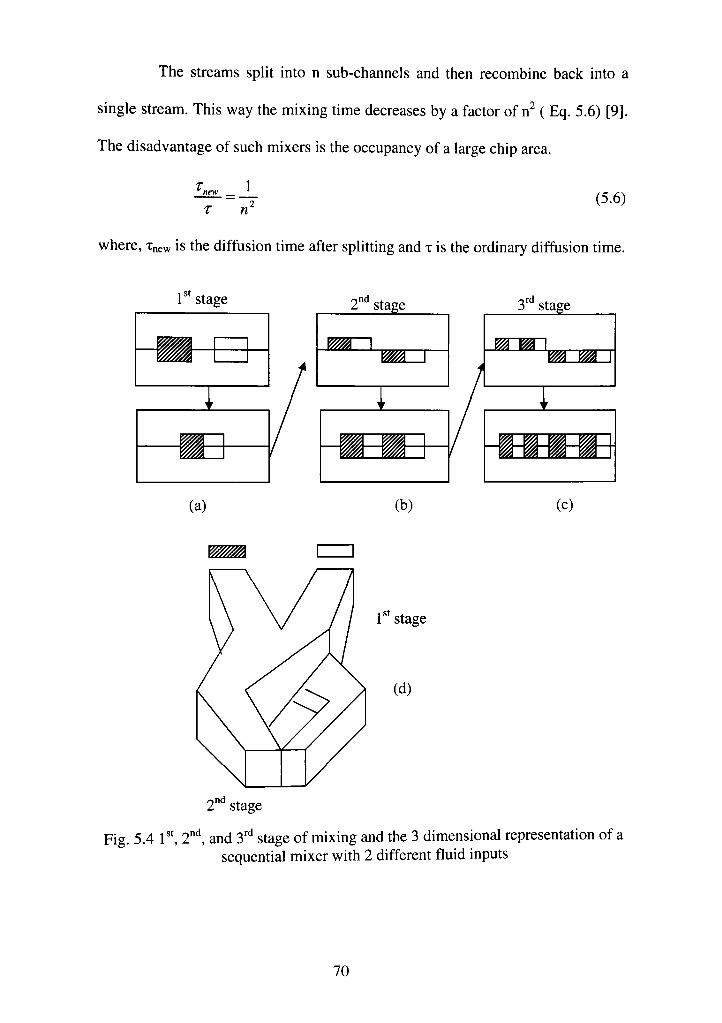
The streams split into n sub-channels and then recombine back into a
single stream. This way the mixing time decreases by a factor of n ( Eq. 5.6) [9].
The disadvantage of such mixers is the occupancy of a large chip area.
(5.6)
where, Tnew is the diffusion time after splitting and x is the ordinary diffusion time.
1"'stage
(a)
2" * stage
(b)
3'^ stage
(c)
nzD
2"* stage
1''stage
(d)
Fig. 5.4 1'*, 2"'^, and 3"* stage of mixing and the 3 dimensional representation of a sequential mixer with 2 different fluid inputs
70
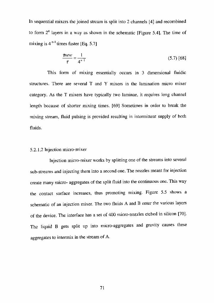
In sequential mixers the joined stream is split into 2 channels [4] and recombined
to form 2" layers in a way as shown in the schematic [Figure 5.4]. The time of
mixing is 4""' times faster [Eq. 5.7]
mew X ,n-\ (5.7) [68]
This form of mixing essentially occurs in 3 dimensional fluidic
structures. There are several T and Y mixers in the lamination micro mixer
category. As the T mixers have typically two laminae, it requires long channel
length because of shorter mixing times. [69] Sometimes in order to break the
mixing stream, fluid pulsing is provided resulting in intermittent supply of both
fluids.
5.2.1.2 Injection micro-mixer
Injection micro-mixer works by splitting one of the streams into several
sub-streams and injecting them into a second one. The nozzles meant for injection
create many micro- aggregates of the split fluid into the continuous one. This way
the contact surface increases, thus promoting mixing. Figure 5.5 shows a
schematic of an injection mixer. The two fluids A and B enter the various layers
of the device. The interface has a set of 400 micro-nozzles etched in silicon [70].
The liquid B gets split up into micro-aggregates and gravity causes these
aggregates to intermix in the stream of A.
71
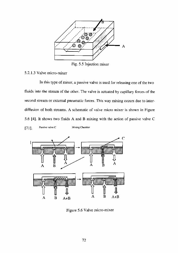
• ^ :r
Fig. 5.5 Injection mixer
5.2.1.3 Valve micro-mixer
In this type of mixer, a passive valve is used for releasing one of the two
fluids into the stream of the other. The valve is actuated by capillary forces of the
second stream or external pneumatic forces. This way mixing occurs due to inter-
diffusion of both streams. A schematic of valve micro mixer is shown in Figure
5.6 [4]. It shows two fluids A and B mixing with the action of passive valve C
ry 1 ] Passive valve C Mixing Chamber
B A+B B A-hB
Figure 5.6 Valve micro-mixer
72
5.2.2 Active micro-mixer
Active mixers use dynamic parts to agitate the fluids and thus promote
mixing. The moving actuators can be externally operated pumps or valves or
some kind of energy source like acoustic or magnetic sources. Primarily, the
active micro-mixers can be categorized into:
• Mixers with pumped fluid inlets,
• Ultrasonic mixer,
• Magneto-hydrodynamic mixers.
5.2.2.1 Mixer with pumped fluid inlets
This design uses pumps to actively improve the mixing of fluids [72]. As
low Reynolds number flow is characteristically symmetrical and reversible,
mixing is usually not possible by external stirring. However, by using a chaotic
flow field generated by external pumps two fluids can be mixed A chaotic flow
field is achieved by a set of two pumps connected via source and sink to the
mixing chamber. The mixing chamber is filled with fluid A at the top and B at the
bottom [Figure 5.7]. After several cycles of pumping through the chamber
complete mixing is attained.
73
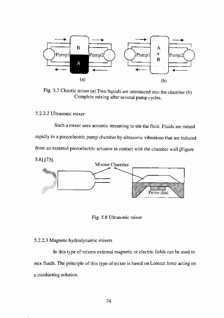
(a) (b)
Fig. 5.7 Chaotic mixer (a) Two liquids are introduced into the chamber (b) Complete mixing after several pump cycles.
5.2.2.2 Ultrasonic mixer
Such a mixer uses acoustic streaming to stir the fluid. Fluids are mixed
rapidly in a piezoelectric pump chamber by ultrasonic vibrations that are induced
from an external piezoelectric actuator in contact with the chamber wall [Figure
5.8] [73]. Mixing Chamber
^%1 €1
Fig. 5.8 Ultrasonic mixer
5.2.2.3 Magneto hydrodynamic mixers
In this type of mixers external magnetic or electric fields can be used to
mix fluids. The principle of this type of mixer is based on Lorenzt force acting on
a conducting solution.
74
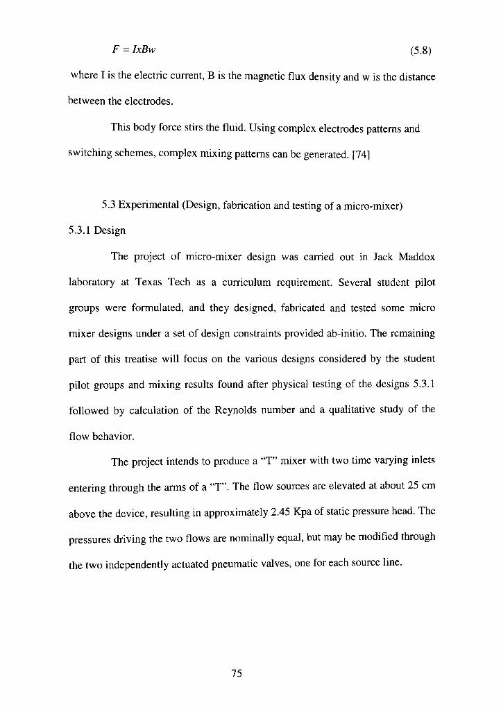
F = IxBw (5.8)
where I is the electric current, B is the magnetic flux density and w is the distance
between the electrodes.
This body force stirs the fluid. Using complex electrodes patterns and
switching schemes, complex mixing patterns can be generated. [74]
5.3 Experimental (Design, fabrication and testing of a micro-mixer)
5.3.1 Design
The project of micro-mixer design was carried out in Jack Maddox
laboratory at Texas Tech as a curriculum requirement. Several student pilot
groups were formulated, and they designed, fabricated and tested some micro
mixer designs under a set of design constraints provided ab-initio. The remaining
part of this treatise will focus on the various designs considered by the student
pilot groups and mixing results found after physical testing of the designs 5.3.1
followed by calculation of the Reynolds number and a qualitative study of the
flow behavior.
The project intends to produce a "T" mixer with two time varying inlets
entering through the arms of a "T". The flow sources are elevated at about 25 cm
above the device, resulting in approximately 2.45 Kpa of static pressure head. The
pressures driving the two flows are nominally equal, but may be modified through
the two independently actuated pneumatic valves, one for each source line.
75
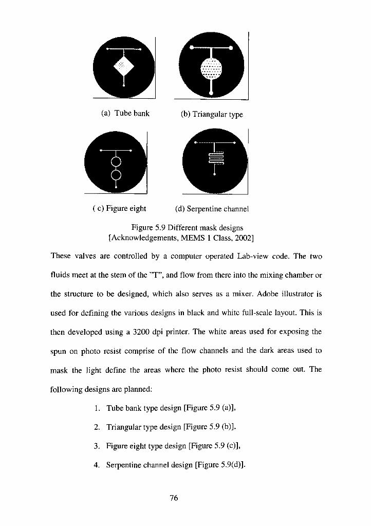
(a) Tube bank (b) Triangular type
(c) Figure eight (d) Serpentine channel
Figure 5.9 Different mask designs [Acknowledgements, MEMS 1 Class, 2002]
These valves are controlled by a computer operated Lab-view code. The two
fluids meet at the stem of the "T", and flow from there into the mixing chamber or
the structure to be designed, which also serves as a mixer. Adobe illustrator is
used for defining the various designs in black and white full-scale layout. This is
then developed using a 3200 dpi printer. The white areas used for exposing the
spun on photo resist comprise of the flow channels and the dark areas used to
mask the light define the areas where the photo resist should come out. The
following designs are planned:
1. Tube bank type design [Figure 5.9 (a)],
2. Triangular type design [Figure 5.9 (b)],
3. Figure eight type design [Figure 5.9 (c)],
4. Serpentine channel design [Figure 5.9(d)].
76
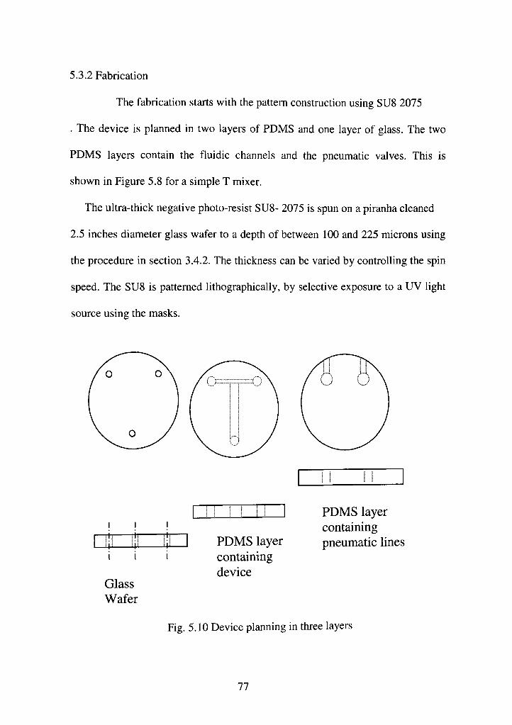
5.3.2 Fabrication
The fabrication starts with the pattern construction using SU8 2075
. The device is planned in two layers of PDMS and one layer of glass. The two
PDMS layers contain the fluidic channels and the pneumatic valves. This is
shown in Figure 5.8 for a simple T mixer.
The ultra-thick negative photo-resist SU8- 2075 is spun on a piranha cleaned
2.5 inches diameter glass wafer to a depth of between 100 and 225 microns using
the procedure in section 3.4.2. The thickness can be varied by controlling the spin
speed. The SU8 is patterned lithographically, by selective exposure to a UV light
source using the masks.
Glass Wafer
PDIVIS layer cont£iining device
PDIVIS layer containing pneumatic lines
Fig. 5.10 Device planning in three layers
77
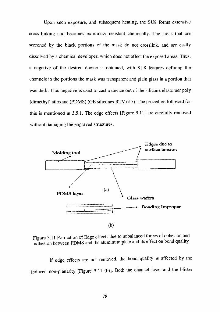
Upon such exposure, and subsequent heating, the SU8 forms extensive
cross-linking and becomes extremely resistant chemically. The areas that are
screened by the black portions of the mask do not crosslink, and are easily
dissolved by a chemical developer, which does not affect the exposed areas. Thus,
a negative of the desired device is obtained, with SU8 features defining the
channels in the portions the mask was transparent and plain glass in a portion that
was dark. This negative is used to cast a device out of the silicone elastomer poly
(dimethyl) siloxane (PDMS) (GE silicones RTV 615). The procedure followed for
this is mentioned in 3.5.1. The edge effects [Figure 5.11] are carefully removed
without damaging the engraved structures.
Molding tool
PDMS layer
Edges due to f .surface tension
Glass wafers
Bonding Improper
(b)
Figure 5.11 Formation of Edge effects due to unbalanced forces of cohesion and adhesion between PDMS and the aluminum plate and its effect on bond quality
If edge effects are not removed, the bond quality is affected by the
induced non-planarity [Figure 5.11 (b)]. Both the channel layer and the blister
78
layers are made in this way. Finally, three 0.75mm holes are drilled into the glass
wafers, one inlet for each fluid and one combined outlet. This glass wafer serves
as a support structure for the device and also helps in attachment of the fluidic
ports. The PDMS fluidic layer and the glass support plate are oxidized in an
Oxygen plasma (Trion Inductively coupled plasma). Immediately upon removal
from the chamber the two pieces are pressed. After bonding process is complete,
the same process is repeated with glass-PDMS. Stainless steel tubes with an
outside diameter of 0.3 mm (McMaster Carr) are inserted into the pneumatic layer
to provide attachments to an off-chip compressed nitrogen gas tank. Barbed
polycarbonate tubing connectors are epoxied to the outside surface of the glass
wafer over the drilled holes to provide access for the mixing stream and an outlet
for the product. The inlet connectors are connected with silicone tubing
(McMaster-Carr) to two bottles containing water, one dyed fluorescent green and
the other undyed. Silicone tubing carries the outlet liquid to a waste beaker. The
pneumatic lines from the two valves are connected, through a Lab-view controlled
solenoid valve, to a bottie of nitrogen gas regulated to 15-20 psi gas pressure.
Figure 5.12 shows the various micro mixer devices developed. Primarily four
types of designs are made as clear form the masks [Figure 5.9 (a) to (d)].
5.3.3 Testing
The Reynolds number of flow in each of these devices has been
calculated with a qualitative visualization of degree of mixing. Surprising and
counter intuitive observations come up on testing of flow behavior through these
devices
79
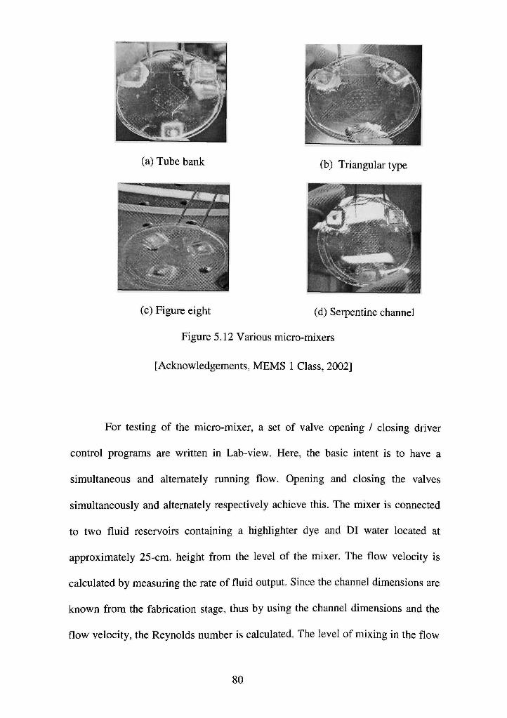
(a) Tube bank (b) Triangular type
(c) Figure eight (d) Serpentine channel
Figure 5.12 Various micro-mixers
[Acknowledgements, MEMS 1 Class, 2002]
For testing of the micro-mixer, a set of valve opening / closing driver
control programs are written in Lab-view. Here, the basic intent is to have a
simultaneous and altemately running flow. Opening and closing the valves
simultaneously and altemately respectively achieve this. The mixer is connected
to two fluid reservoirs containing a highlighter dye and DI water located at
approximately 25-cm. height from the level of the mixer. The flow velocity is
calculated by measuring the rate of fluid output. Since the channel dimensions are
known from the fabrication stage, thus by using the channel dimensions and the
flow velocity, the Reynolds number is calculated. The level of mixing in the flow
80
is also observed by eyes and microscope, photographed and filmed respectively.
The highlighter dye shines on being illuminated by a UV source. Thus, as mixing
takes place, the shine is dimmed as the concentration of dye in the mixture
decreases.
5.4 Results and discussion
The first two designs are the "tube bank type design" and the "Triangle"
design. Both these promote little or no mixing. The input streams after entering
the chamber run out of the exit side parallel without any substantial change in the
coloration. There is no inter-diffusion of species at the molecular level as they
move in parallel laminae. Although the design promotes eddies and vortices in the
flow and a laminar boundary layer, developed about the rough inside of the mixer
trips, but it happens so far away from the interface of two streams that they cause
insignificant mixing. Slight mixing is seen as the flow is made time varying using
lab-view controlled pneumatic valve set. This is primarily because, as both layers
move parallel to each other with a different velocity, there is a high shear rate
between the layers promoting mixing. The flow velocity in the stem of the "T" is
monitored and found to be 2.84 mm/sec and 3.97mm/sec respectively. Also the
wetted perimeter to area ratio in this case is .00074. Thus Reynolds number is
calculated using Eq. 5.1 and 5.2 and found to be 1.86 E-03 and 2.59 E-03. The
Reynolds numbers for the remaining designs are calculated to be within the same
range. This explains the highly laminar nature of the flow and also the reasons for
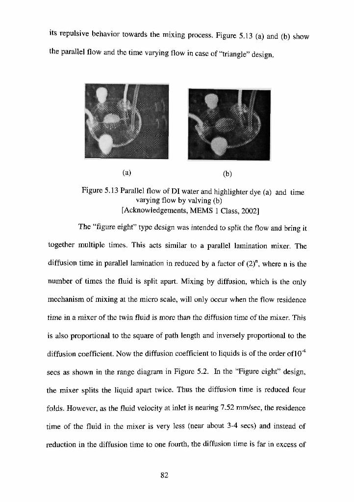
Its repulsive behavior towards the mixing process. Figure 5.13 (a) and (b) show
the parallel flow and the time varying flow in case of "triangle" design.
(a) (b)
Figure 5.13 Parallel flow of DI water and highlighter dye (a) and time varying flow by valving (b)
[Acknowledgements, MEMS 1 Class, 2002]
The "figure eight" type design was intended to split the flow and bring it
together multiple times. This acts similar to a parallel lamination mixer. The
diffusion time in parallel lamination in reduced by a factor of (2)", where n is the
number of times the fluid is split apart. Mixing by diffusion, which is the only
mechanism of mixing at the micro scale, will only occur when the flow residence
time in a mixer of the twin fluid is more than the diffusion time of the mixer. This
is also proportional to the square of path length and inversely proportional to the
diffusion coefficient. Now the diffusion coefficient to liquids is of the order oflO'^
sees as shown in the range diagram in Figure 5.2. In the "Figure eight" design,
the mixer splits the liquid apart twice. Thus the diffusion time is reduced four
folds. However, as the fluid velocity at inlet is nearing 7.52 mnVsec, the residence
time of the fluid in the mixer is very less (near about 3-4 sees) and instead of
reduction in the diffusion time to one fourth, the diffusion time is far in excess of
82
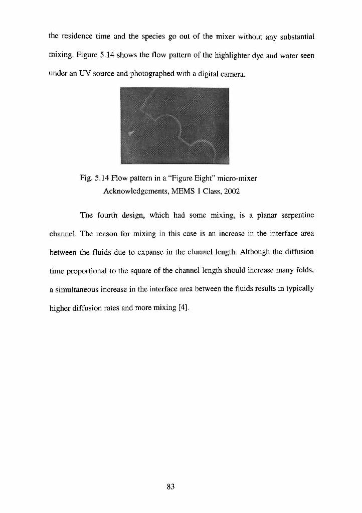
the residence time and the species go out of the mixer without any substantial
mixing. Figure 5.14 shows the flow pattern of the highlighter dye and water seen
under an UV source and photographed with a digital camera.
Fig. 5.14 Flow pattern in a "Figure Eight" micro-mixer
Acknowledgements, MEMS 1 Class, 2002
The fourth design, which had some mixing, is a planar serpentine
channel. The reason for mixing in this case is an increase in the interface area
between the fluids due to expanse in the channel length. Although the diffusion
time proportional to the square of the channel length should increase many folds,
a simultaneous increase in the interface area between the fluids results in typically
higher diffusion rates and more mixing [4].
83
CHAPTER 6
CONCLUSIONS AND RECOMMENDATION
The originally hydrophobic surface of PDMS becomes hydrophilic upon
oxygen plasma treatment under certain process conditions. We have found that a
uniform oxygen plasma exposure of lower RF power with shorter duration makes
a thin layer of undamaged oxide on the surface of PDMS with active silanol
groups that largely facilitate in obtaining an irreversible sealing. The results
follow a general trend in terms of bond strength and contact angle measured on
plasma treated surfaces. It is observed that one gets stronger bonding as contact
angle decreases subsequently when PDMS or glass is treated by O2 plasma. An
excellent correlation between different plasma parameters and surface wettability
of PDMS or glass surface measured in terms of contact angle is found. All the
results indicate that a contact angle below 5 degree is a general requirement for
getting very good bond strength and thereby one can obtain the correct plasma
parameters for surface treatment by investigating and monitoring contact angle. A
nice correlation has been obtained between surface roughness and bond strength
of PDMS-PDMS and PDMS-glass bond. The fall in bond strength with increasing
surface roughness is greater in case of glass-PDMS for reasons, already discussed.
Thus contact angle becomes a new scale of reference for measurement of bond
strength. The oxygen plasma parameters developed have been successfully used
in stacking together and irreversibly bonding the multiple layers of glass and
replica molded PDMS. Such a technique has been used to build several designs of
84
parallel lamination micro-mixers. Flow behavior has been qualitatively studied in
such designs. The results, which come are very different from real life macro
scale mixers, which primarily use turbulence for better and quicker mixing. The
mixers show that the success of mixing at the micro-scale is primarily attributed
to inter-diffusion of molecular species. The results show an altogether different
regime of mixing, which can be utilized in future designing of refined versions of
these micro-mixers.
A software package can be envisioned for future with a correct statistical
foundation wherein using design of experiments, and specifying contact angle the
exposure dose can be gauged. Thus for any new plasma etcher the correct set of
parameters can be obtained by specifying an angle below 5° and the other
parameters which are kept constant during the process such as the inductively
coupled plasma power, the oxygen flow rate, the chamber size, etc.
85
REFERENCES
1. Stephen D. Centuria, Microsystem Design. Kluwer Academic Publishers, Boston / Dordrecht / London, 2001.
2. W.S. Trimmer, Editor, Micromechanics and MEMS: Classical and Seminal Papers to 1990. IEEE Press, Piscataway, NJ, 1997.
3. "Miniaturized total chemical analysis system: A novel Concept for chemical sensing," Sensors and Actuators B, Manz, A., Graber, N., and Widmer, H.M., Vol.1, 1990,pp.244-248.
4. N.-T. Nguyen and S. T. Werely, Fundamentals and Applications of Microfluidics, Artech House, Boston, 2002.
5. The mechanisms of hydrophobic recovery of polydimethylsiloxane elastomers exposed to partial electrical discharges, Kim J, Chaudhury MK, Owen MJ, Orbeck T., Journal of Colloid and hiterface Science, 244 (1): 200-207, DEC 1,2001.
6. Chaudhury MK, Self assembled monolayers on Polymer surfaces. Biosensors & Bioelectronics 10(9-10): 785-788, 1995.
7. Ma X.,Cierhart, Collins S.D., Smith R.L., Low temperature bonding for wafer scale packaging and assembly of micromachined sensors paper, Final Report 1998-99 for MICRO Project 98-144 Industrial Sponsor(s): Kumetrix, Inc.
8. Younan Xia and George Whitesides, Soft lithography, Angew. Chem. Int. Ed. 1998, 37.
9. General reviews on photoUthography: a) S. Okazaki, J. Vac. Sci.Technol. B 1991, 9, 2829 -2833; b) H. J. Jeong, D. A. Markle, G.Owen, F. Pease, A. Grenvill'e, R. von B.nau, Solid State Technol.1994, 37, 39 47; c) M. D. Levenson, ibid. 1995 , 38, 57 66; d) L.Geppert, IEEE Spectrum 1996, 33(4), 33 ± 38.Actuators A 1994, 41/42, 593 - 596.
10 Cast molding on the micrometer scale: a) H. C. Haverkom van Rijsewijk, P. ' E J Legierse, G. E. Thomas, Philips Tech. Rev. 1982, 40,287 - 297; b) J. G. Kloosterboer,' G. J. M. Lippits, H. C. Meinders, ibid. 1982, 40, 198 309.
11 B. D. Terris, H. J. Mamin, M. E. Best, J. A. Logan, D. Rugar, Cast molding " on the nanoiiieter scale, Appl. Phys. Lett. 1996, 69, 4262 - 4264.
86
12. Allen MG, Senturia SD, Analysis of critical debonding pressures of stressed thin films in the blister test. Journal of Adhesion 25(4): 303-305, 1988.
13. Dr. Arindam Dutta, Personal communication, Nanotech Center, Texas Tech university, 2002.
14. Mechanisms of Anodic bonding of silicon to Pyrex glass, Kevin B. Albaugh, IBM general technology division, Essex Junction, VT 05452, Don H ' Rasmussen, Department of chemical engineering, Clarkson University, Potsdam. NY 13676.Langmuir I. and Mott-Smith H.M., Physics Review 28 727(1926).
15. Yasuda H.K., Plasma polymerization and plasma treatment of polymers. Journal of Applied polymer science. Applied Polymer Symposia 42, April, 1987, Interscience Publication.
16. Boley Forrest I., Plasmas -laboratory and cosmic, D. Van Nostrand Company, Inc., Princeton, New Jersey, 1996.
17. Auerbach R.A., Tuma D.T. and Blenner D.R., Lord Corporation, March, 1978, Carnegie Mellon University, Pittsburgh.
18. Campbell, Stephen A., Science of Microelectronic Fabrication, Oxford University Press, New York, 1996
19. Chapman B., Glow Discharge Processes, Wiley, New York (1980).
20. Spitzer Lyman, Jr., Physics of fully ionized gases, Interscience Publishers, New York, 1962.
21.Sugawara M., Plasma Etching-Fundamentals and Applications, Oxford University Press, Tokyo, 1988.
22. Manabu Tokeshi, Kichi Sato and Tahehiko Kitamori, Integration chemistry for bio chip: Integration of immunoassay and biochemical lab on chip, Kanagawa academy of science and technology. Department of applied chemistry. Graduate school of Engineering, University of Tokyo, 1995
23. Ranjith Ranganathan, Personal communication. Graduate student Electrical Engineering Department, Texas Tech University, 2003.
24. Morgan, R.A., Plasma Etching in Semiconductor Fabrication, Elsevier, Amsterdam, 1985.
25. Manos, D.M., Flamm, D.L., Plasma Etching, an introduction. Academic Press, Boston, 1989.
87
26. Ephrath, L.M. and Petrillo, E.J., Parameter and reactor dependence of selective Oxide RIE in CF4 and O2 plasma. Journal of Electrochemical Society, 129:2282(1982).
27. Boumans, P.W.J.M., Inductively coupled plasma emission spectroscopy, Interscience publication, New York, 1993.
28. Service and warranty manual ,Trion Technologies, 1998. www.triontech.com
29. Adamson, Arthur W., Physical chemistry of surfaces, Interscience publication. New York, 1983.
30. Hydrophobicity changes in Silicone rubbers, Hillborg H., Gedde U.W., IEEE transactions on dielectrics and electrical insulation, Vol. 6 No. 5, October 1999.
31. Ristic, L., ed.. Sensor technology and devices, Artech House Boston, MA., (1994).
32. Chan, J.H., A.T. Timperman, D. Qin and R. Aebersold. Microfabricated Polymer Devices for Automated Sample Delivery of Peptides for Analysis by Electrospray Ionization Tandem Mass Spectrometry, Analytical Chemistry, vol. 71, no. 20, pp.4437-4444 (1999).
33. Material safety datasheet, Microchem, 1254, Chestnut Street, Newton, MA, 2002.
34. JSR materials for C4 processes, JSR Corporation. Specialty Materials Laboratory Fine Electric Research Laboratories, ApiA semicon west seminar, 1996.
35. Alexei L. Bogdanov, Use of SU-8 Negative Photoresist for Optical Mask Manufacturing, MAX-Lab, University of Lund, SE-221 00, Lund, Sweden, 1996.
36. Michael Koch, Alan Evans, Arthur Brunnschweiler, Microfluidic Technology and applications. Research Studies Press Ltd., Baldock, Hertfordshire, England, 1998.
37. Nano TM SU8 2000, negative tone photoresist, formulations 2030-2100, Microchem, 1254, Chestnut Street, Newton, MA.
38 N.-T. Nguyen and S. T. Werely, Fundamentals and applications of Microfluidics, Artech House, Boston, 2002.
88
39. Armani, D., C. Liu and N. Alum (1998) "Re-configurable fluid circuits by PDMS Elastomer Microm achining, "12"^ MEMS, MEMS-1999, pp. 222-227, Orlan, EL PDMS Elastomer Microm achining, "12"^ International Conference on
40. Wilbur, J. L., A. Kumar, E. Kim and G.M. Whitesides (1994) Advanced Materials, 6, pp. 600-604.
41. Sean O'Brien, On MEMS talk , Sci. Chem.(1997), http://mail.mems-exchange.org/pipermail/mems-talk/.
42. Standard operating procedure Microsystem Technology Laboratories MIT, Bldg-39Room, 32160, VassarStreet, Cambridge, MA 02139,2001.
43. Home page of Solid state equipment corporation, Horsham, PA San Jose. www.ssecusa.com
44. Michial Duff, Actively enhanced etch fabrication and application of optical fiber capillary devices in the 300-500 Mhz Range by Howell. http://acoustics.stanford.edu/IRP/duffthesis
45. Homepage of Analytical Instmments,LLC1200 Mendelssohn Avenue, Suite 50, Golden Valley, MN 55427-4366. www.aibltd.com
46. Homepage Headway Research, Inc. 3713, Forest Lane Garland, TX 75042-6928 USA. www.pitt.edu/AFShome/g/i/gilbertw/ public/html/jason/links
47. Madou, M.,Fundamentals of microfabrication, CRC Press, Boca Raton F.L., (1997).
48. Dannenberg. H, Phenyl-bridging in the 2-phenylethyl radical. A molecular orbital study, Joumal of Organic Chemistry, 66 (18): 5996-5999 (2001).
49. Hinkley, J.A., Oxidative aging of cured polymer from phyenylethynyl terminated imide oligomers, Joumal of Adhesion, 16, 115-125 (1983).
50. Allen, M.G., and Senturia, S.D., Proceedings of the American Chemical Society Division of Polymeric Materials: Science and Engineering 56, 735-739 (1987).
51. Gent A.N., Zhang L.Q., Strain-induced crystallization and strength of elastomers I. cis-l,4-polybutadiene, Joumal of polymer science phys 39 (7), pp. 811-817,2001.
52. Home page of smg diamond company (www.smg-diamond.com/lapping )
89
53. R. R. Kunz, H. R. Clark, P. M. Nitishin, and M. Rothschild, Lincoln Laboratory, Massachusetts Institute of Technology, Lexington, Massachusetts 02173-9108, B. S. Ahem, Rome Air Development Center, Hanscom Air Force Base, Massachusetts 07131-5000, High resolution studies of crystalline damage induced by lapping and single point diamond machining, 1999.
54. NT 1100,Users manual, Veeco Systems for Research, 100-1039-17th Ave, S.W. Suite 405 Calgary, Alberta T2T 0B2,1996.
55. Plasma treatment of Poly (dimethyl) silaxane, Owen M.J., Smith P.J., Joumal of adhesion science and technology, Vol.8, No. 10, pp. 1063-1075, 1994.
56. Hydrophobicity changes in Silicone mbbers, Hillborg H., Gedde U.W., IEEE transactions on dielectrics and electrical insulation. Vol. 6 No. 5, October 1999.
57. Siloxane polymers by Stephen J. Clarson and J. Anthony Semlyen, Ellis Horwood- PTR Prentice Hall, 1996, www.prenhall.com.
58. Henry, S., et. al., Micromachined needles for transdermal delivery of dmgs, proceedings for MEMS' 98, 11* IEEE intemational workshop microelectromechanical systems, Heidelberg, Germany, Jan 25-28, 1998, pp. 494-498.
59. Madou, M., Fundamentals of microfabrication, CRC Press, Boca Raton., 1997.
60. P.G. Drazin, Introduction to hydrodynamic stability, Cambridge University Press, Cambridge, UK,2002.
61. Frank, M., White, Fluid mechanics, McGraw-Hill Companies, New York, 1992.
62. R.W. Fox and A.T. McDonald, "Introduction to fluid mechanics", 5* Edition, John Wiley and Sons, New York, 1998.
63. N.-T. Nguyen and S. T. Werely, Fundamentals and Applications of Microfluidics, Artech House, Boston, 2002.
64. Cussler, E.L., Diffusion Mass Transfer in the Fluid Systems, Cambridge University press. New York, 1984.
65 Erbacher, C , et al.. Towards Integrated Continuous Flow chemical reactors, ' Mikrochi'mic'a Acta', Vol. 131, 1999, pp. 19-24.
90
66. Deshmukh, A.A., Liepmann, D., and Pisano, A.P., Characterization of a micro mixing, pumping, and valving systems, Proceedings of transducers '01, 11* International Conference on solid state sensors and actuators, Germany, June 6-7, 2001, pp. 779-782.
67. Deshmukh, A.A., Liepmann, D., and Pisano, A.P, Continuous Micromixer with pulsatile micropump. Technical digest of the IEEE solid state sensors and actuators workshop, Hilton head island, SC, June 4-8, 2000, pp. 73-76.
68. Larsen, U.D., Rong, W.,Telleman P., Design of rapid micro mixers using CFD," Proceedings of transducers 99, 10* intemational conference on solid state sensors and actuators, Sendai, Japan, June 7-10, 1999, pp. 200-203.
69. Seidel. R.U., et al., "Capillary force mixing device as sampling module for chemical analysis," Proceedings of transducers '99, 10* intemational conference on solid state sensors and actuators, Sendai, Japan, June 7-10, 1999,pp.438-441.
70. Evans, J., Liepmann, D., and Pisano, A.P, "Planar laminar mixer. Proceedings of MEMS 97, 10* IEEE Intemational workshop micro electro mechanical system, Nagoya, Japan, Jan 26-30, 1997, pp. 96-101.
71.Woias, P., Hauser, K., and Yacoub- George, E., "An active silicon micrimixer for microTAS applications," Micrototal Analysis System 2000, A. van den Berg et. al.(eds.), Boston, MA: Kluwer Academic publishers, 2000, pp.227-282
72. Bau, H.H., Zhong, J., Yi, M., A minute magneto hydrodynamic mixer, ' Sensors and actuators B, Vol.79, No.2-3, 2001, pp. 207-215.

APPENDIX A
Physical properties of SU8 (Photoresist)
92
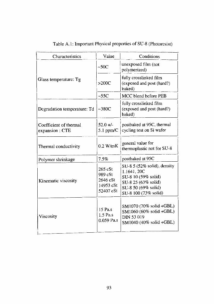
Table A. 1: Important Physical properties of SU-8 (Photoresist)
Characteristics Value Conditions
Glass temperature: Tg
-50C unexposed film (not polymerized)
>200C
-55C
fully crosslinked film (exposed and post (hard?) baked)
MCC blend before PEB
Degradation temperature: Td ~380C fully crosslinked film (exposed and post (hard?) baked)
Coefficient of thermal expansion : CTE
52.0 +1-5.1 ppm/C
postbaked at 95C, thermal cycling test on Si wafer
Thermal conductivity
Polymer shrinkage
Kinematic viscosity
Viscosity
0.2 W/mK general value for thermoplastic not for SU-8
7.5%
265 cSt 989 cSt 2646 cSt 14953 cSt 52407 cSt
15 Pa.s 1.5Pa.s 0.059 Pa.s
postbaked at 95C
SU-8 5 (52% solid), density 1.1641, 20C SU-8 10 (59% solid) SU-8 25 (63% solid) SU-8 50 (69% solid) SU-8 100 (73% solid)
SMI070 (70% solid +GBL) SMI060 (60% solid +GBL) DIN 53 019 SMI040 (40% solid +GBL)
93

APPENDIX B
Theoritical calculation of bond strength
94
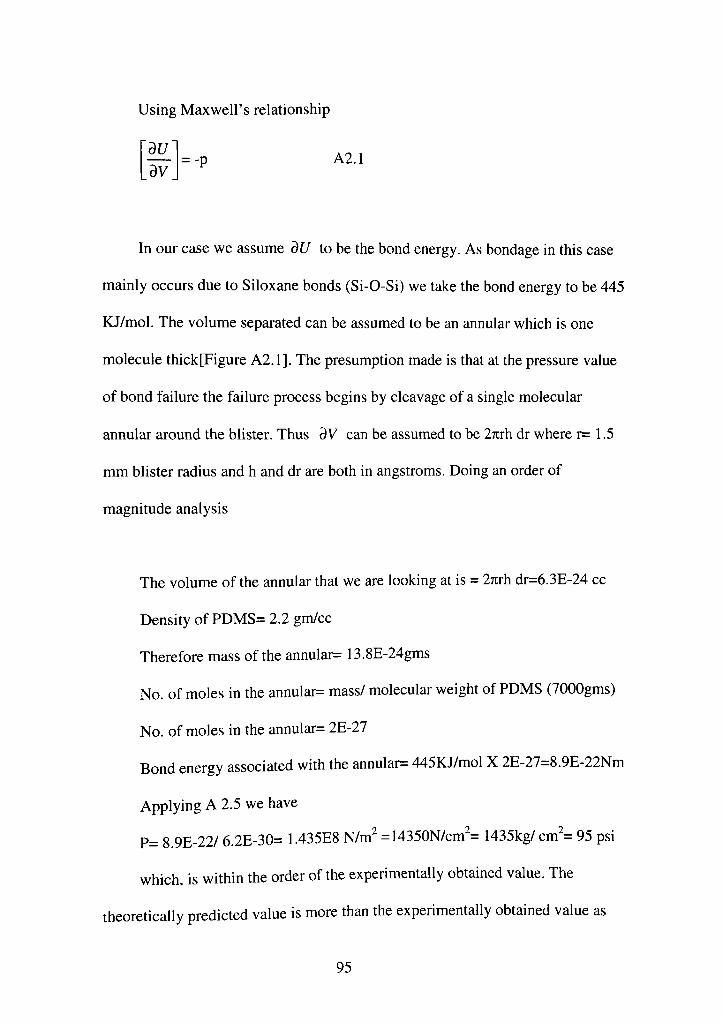
Using Maxwell's relationship
dV = -p A2.1
In our case we assume dU to be the bond energy. As bondage in this case
mainly occurs due to Siloxane bonds (Si-O-Si) we take the bond energy to be 445
KJ/mol. The volume separated can be assumed to be an annular which is one
molecule thick[Figure A2.1]. The presumption made is that at the pressure value
of bond failure the failure process begins by cleavage of a single molecular
annuleir around the blister. Thus dV can be assumed to be 27irh dr where r= 1.5
mm blister radius and h and dr are both in angstroms. Doing an order of
magnitude analysis
The volume of the annular that we are looking at is = 27rrh dr=6.3E-24 cc
Density of PDMS= 2.2 gm/cc
Therefore mass of the annular= 13.8E-24gms
No. of moles in the annular= mass/ molecular weight of PDMS (7000gms)
No. of moles in the annular= 2E-27
Bond energy associated with the annular= 445KJ/mol X 2E-27=8.9E-22Nm
Applying A 2.5 we have
P= 8.9E-22/ 6.2E-30= 1.435E8 N/m^ =14350N/cm^= 1435kg/ cm^= 95 psi
which, is within the order of the experimentally obtained value. The
theoretically predicted value is more than the experimentally obtained value as
95
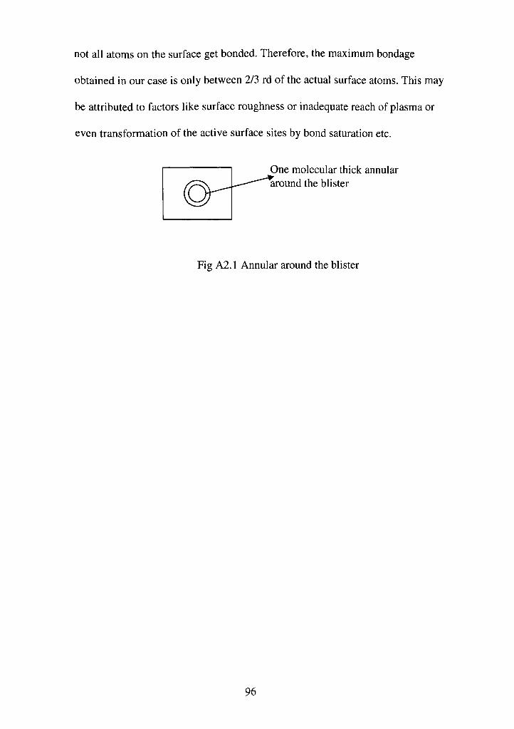
not all atoms on the surface get bonded. Therefore, the maximum bondage
obtained in our case is only between 2/3 rd of the actual surface atoms. This may
be attributed to factors like surface roughness or inadequate reach of plasma or
even transformation of the active surface sites by bond saturation etc.
One molecular thick annular around the blister
Fig A2.1 Annular around the blister
96
PERMISSION TO COPY
In presenting this thesis in partial fulfillment of the requirements for a
master's degree at Texas Tech University or Texas Tech University Health Sciences
Center, I agree that the Library and my major department shall make it freely
available for research purposes. Permission to copy this thesis for scholarly purposes
may be granted by the Director of the Library or my major professor. It is
understood that any copying or publication of this thesis for financial gain shall not
be aUowed without my further written permission and that any user may be liable for
copyright infringement.