Embed Size (px)
Citation preview

Via dell' Artigiano, 8/640016 San Giorgio di Piano(Bologna) ITALYE-mail: [email protected]
http://www.grifo.it http://www.grifo.comTel. +39 051 892.052 (a.r.) FAX: +39 051 893.661
, GPC®, grifo ®, are trade marks of grifo ®
TECHNICAL MANUAL
grifo ®
ITALIAN TECHNOLOGY
GPC® R/T168 Edition 5.00 Rel. 07 February 2001
GPC® R/T168General Purpose Controller
Relays or Transistors; 16 Inputs, 8 Outputs
ABACO® Block M Serie size 22.5x82x90 mm. Housing for Omega railDIN 46277-1 and DIN 46277-3 types.Available in 3 different versions with the following CPUs:
GPC® R/T168 with Atmel 89C52 22MHz, 32K external SRAMGPC® R/T168A with Atmel 89S8252 22MHz; 8K internal FLASH;
2K internal EEPROM; 32K external SRAMGPC® R/T168P with Philips 89C51Rx2 22MHz; from 16K to 64K
internal FLASH; from 512 bytes to 1K internalSRAM; 32K external SRAM; serial ISP Flashprogramming through RS 232
Total addressable memory is 96K divided in: 32K static RAM soldered;64K Flash EPROM inside the microcontroller; code compatible withfamily 51 µP; Real Time Clock with 256 Byte of internal SRAM; Back upcircuitry for RTC and SRAM, through LITHIUM battery; Real Time Clockoutput for /INT management or frequency output; 16 NPN digital inputlines, galvanically isolated: 8 of them are connected to the microcontrollerand 8 are connected to PCF8575 that generates INT ad whenever inputschange; 8 output relays 5A; 4 A/D lines and one 8 bit D/A through PCF8591; I/O connections through quick release screw terminal connectors;3 timer counter resolution16 bits; serial lines in RS232, or in RS422, RS485or Current-Loop; supply of the galvanically isolated section: +24 Vdc;supply of the on board logic: 5Vdc or 10÷40 Vdc or 8÷24Vac; supplyprotection through TransZorb™ ; wide range of development softwareavailable like C compilers, Assembler, BXC51, MCS BASIC 52, HTC51, BASCOM 8051, PASCAL, CMX , etc.
DOCUMENTATION COPYRIGHT BY grifo ® , ALL RIGHTS RESERVED
No part of this document may be reproduced, transmitted, transcribed, stored in aretrieval system, or translated into any language or computer language, in any form orby any means, either electronic, mechanical, magnetic, optical, chemical, manual, orotherwise, without the prior written consent of grifo ®.
IMPORTANT
Although all the information contained herein have been carefully verified, grifo ®
assumes no responsability for errors that might appear in this document, or for damageto things or persons resulting from technical errors, omission and improper use of thismanual and of the related software and hardware.grifo ® reserves the right to change the contents and form of this document, as well as thefeatures and specification of its products at any time, without prior notice, to obtainalways the best product.For specific informations on the components mounted on the card, please refer to theData Book of the builder or second sources.
SYMBOLS DESCRIPTION
In the manual could appear the following symbols:
Attention: Generic danger
Attention: High voltage
Trade Marks
, GPC®, grifo ® : are trade marks of grifo ®.Other Product and Company names listed, are trade marks of their respective companies.
ITALIAN TECHNOLOGY grifo ®
Page I GPC® R/T168 Rel. 5.00
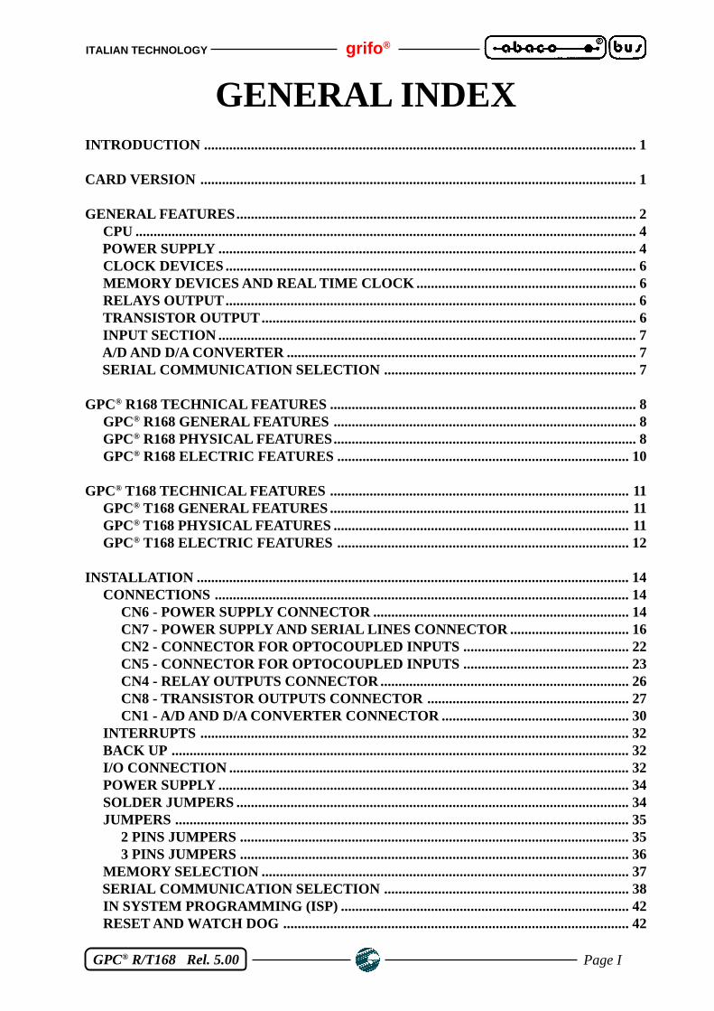
GENERAL INDEXINTRODUCTION ........................................................................................................................ 1
CARD VERSION ......................................................................................................................... 1
GENERAL FEATURES...............................................................................................................2 CPU ........................................................................................................................................... 4 POWER SUPPLY .................................................................................................................... 4 CLOCK DEVICES .................................................................................................................. 6 MEMORY DEVICES AND REAL TIME CLOCK ............................................................. 6 RELAYS OUTPUT.................................................................................................................. 6 TRANSISTOR OUTPUT........................................................................................................ 6 INPUT SECTION .................................................................................................................... 7 A/D AND D/A CONVERTER ................................................................................................. 7 SERIAL COMMUNICATION SELECTION ...................................................................... 7
GPC® R168 TECHNICAL FEATURES ..................................................................................... 8 GPC® R168 GENERAL FEATURES .................................................................................... 8 GPC® R168 PHYSICAL FEATURES.................................................................................... 8 GPC® R168 ELECTRIC FEATURES ................................................................................. 10
GPC® T168 TECHNICAL FEATURES ................................................................................... 11 GPC® T168 GENERAL FEATURES ................................................................................... 11 GPC® T168 PHYSICAL FEATURES .................................................................................. 11 GPC® T168 ELECTRIC FEATURES ................................................................................. 12
INSTALLATION ........................................................................................................................ 14 CONNECTIONS ................................................................................................................... 14 CN6 - POWER SUPPLY CONNECTOR ....................................................................... 14 CN7 - POWER SUPPLY AND SERIAL LINES CONNECTOR ................................. 16 CN2 - CONNECTOR FOR OPTOCOUPLED INPUTS .............................................. 22 CN5 - CONNECTOR FOR OPTOCOUPLED INPUTS .............................................. 23 CN4 - RELAY OUTPUTS CONNECTOR ..................................................................... 26 CN8 - TRANSISTOR OUTPUTS CONNECTOR ........................................................ 27 CN1 - A/D AND D/A CONVERTER CONNECTOR .................................................... 30 INTERRUPTS ....................................................................................................................... 32 BACK UP ............................................................................................................................... 32 I/O CONNECTION ............................................................................................................... 32 POWER SUPPLY .................................................................................................................. 34 SOLDER JUMPERS ............................................................................................................. 34 JUMPERS .............................................................................................................................. 35 2 PINS JUMPERS ............................................................................................................ 35 3 PINS JUMPERS ............................................................................................................ 36 MEMORY SELECTION ...................................................................................................... 37 SERIAL COMMUNICATION SELECTION .................................................................... 38 IN SYSTEM PROGRAMMING (ISP) ................................................................................ 42 RESET AND WATCH DOG ................................................................................................ 42
grifo ® ITALIAN TECHNOLOGY
Page II GPC® R/T168 Rel. 5.00
SOFTWARE ................................................................................................................................ 43
ADDRESSING ............................................................................................................................ 44 INTRODUCTION ................................................................................................................. 44 ON BOARD RESOURCES ADDRESSING ....................................................................... 44 I2C-BUS PERIPHERALS MAPPING ................................................................................. 44
PERIPHERAL DEVICES SOFTWARE DESCRIPTION ..................................................... 46 BACKED SRAM + RTC....................................................................................................... 46 SERIAL EEPROM ................................................................................................................ 46 4 A/D AND 1 D/A ................................................................................................................... 47 I/O EXPANDER .................................................................................................................... 48 DIGITAL INPUTS................................................................................................................. 49 DIGITAL OUTPUTS ............................................................................................................ 49 CPU PERIPHERALS ...........................................................................................................49
BIBLIOGRAPHY....................................................................................................................... 50
ALPHABETICAL INDEX ...................................................................................................... A-1

ITALIAN TECHNOLOGY grifo ®
Page III GPC® R/T168 Rel. 5.00
FIGURES INDEXFIGURE 1: GPC® R168 BLOCK DIAGRAM ......................................................................................... 3FIGURE 2: GPC® T168 BLOCK DIAGRAM ......................................................................................... 5FIGURE 3: GPC® R168 (COMPONENT SIDE) COMPONENTS MAP ......................................................... 9FIGURE 4: GPC® R168 (SOLDER SIDE) COMPONENTS MAP ................................................................ 9FIGURE 5: GPC® T168 (COMPONENT SIDE) COMPONENTS MAP ....................................................... 13FIGURE 6: GPC® T168 (SOLDER SIDE) COMPONENTS MAP .............................................................. 13FIGURE 7: CN6 - POWER SUPPLY CONNETTOR ................................................................................ 14FIGURE 8: GPC® R168 CONNECTORS, ETC. LOCATION .................................................................... 15FIGURE 9: GPC® T168 CONNECTORS, ETC. LOCATION .................................................................... 15FIGURE 10: CN7 - POWER SUPPLY AND SERIAL LINES CONNECTOR ................................................... 16FIGURE 11: SERIAL COMMUNICATION DIAGRAM ............................................................................... 17FIGURE 12: RS 232 POINT TO POINT CONNECTION EXAMPLE ........................................................... 17FIGURE 13: RS 422 POINT TO POINT CONNECTION EXAMPLE ........................................................... 18FIGURE 14: RS 485 POINT TO POINT CONNECTION EXAMPLE ........................................................... 18FIGURE 15: RS 485 NETWORK CONNECTION EXAMPLE .................................................................... 19FIGURE 16: 4 WIRES CURRENT LOOP POINT TO POINT CONNECTION EXAMPLE .................................. 20FIGURE 17: 2 WIRES CURRENT LOOP POINT TO POINT CONNECTION EXAMPLE .................................. 20FIGURE 18: PASSIVE CURRENT LOOP NETWORK CONNECTION EXAMPLE .......................................... 21FIGURE 19: CN2 - CONNECTOR FOR OPTOCOUPLED INPUTS ............................................................ 22FIGURE 20: CN5 - CONNECTOR FOR OPTOCOUPLED INPUTS ............................................................ 23FIGURE 21: OPTOCOUPLED INPUTS BLOCK DIAGRAM ....................................................................... 24FIGURE 22: GPC® R168 CARD PHOTO ........................................................................................... 25FIGURE 23: CN4 - RELAY OUTPUTS CONNECTOR ............................................................................ 26FIGURE 24: RELAY OUTPUTS DIAGRAM ............................................................................................ 27FIGURE 25: CN4 - TRANSISTOR OUTPUTS CONNECTOR .................................................................... 28FIGURE 26: TRANSISTOR OUTPUTS BLOCK DIAGRAM ........................................................................ 29FIGURE 27: CN1 - A/D AND D/A CONVERTER CONNECTOR ............................................................. 30FIGURE 28: A/D INPUT AND D/A CONVERTER OUTPUT BLOCK DIAGRAM ........................................... 31FIGURE 29: GPC® T168 CARD PHOTO ........................................................................................... 33FIGURE 30: JUMPERS SUMMARIZING TABLE ..................................................................................... 35FIGURE 31: 2 PINS JUMPERS TABLE ................................................................................................. 35FIGURE 32: 3 PINS JUMPERS TABLE ................................................................................................. 36FIGURE 33: GPC® R168 JUMPERS LOCATION ON COMPONENT SIDE ................................................. 36FIGURE 34: GPC® R168 JUMPERS LOCATION ON SOLDER SIDE ........................................................ 37FIGURE 35: MEMORY SELECTION TABLE ......................................................................................... 37FIGURE 36: GPC® T168 JUMPERS LOCATION ON COMPONENT SIDE ................................................. 39FIGURE 37: GPC® T168 JUMPERS LOCATION ON SOLDER SIDE ........................................................ 39FIGURE 38: SERIAL COMMUNICATION DRIVERS LOCATION ................................................................ 41FIGURE 39: I2C-BUS PERIPHERALS ADRESSING TABLE ................................................................... 44FIGURE 40: MEMORY ADDRESSING TABLE ....................................................................................... 45FIGURE 41: A/D AND D/A CONTROL REGISTERS .............................................................................. 48FIGURE 42: POSSIBLE CONNECTIONS DIAGRAM ................................................................................ 51

grifo ® ITALIAN TECHNOLOGY
Page IV GPC® R/T168 Rel. 5.00

ITALIAN TECHNOLOGY grifo ®
Page 1 GPC® R/T168 Rel. 5.00
INTRODUCTIONINTRODUCTION
The use of these devices has turned - IN EXCLUSIVE WAY - to specialized personnel.
The purpose of this handbook is to give the necessary information to the cognizant and sure use ofthe products. They are the result of a continual and systematic elaboration of data and technical testssaved and validated from the manufacturer, related to the inside modes of certainty and quality ofthe information.
The reported data are destined- IN EXCLUSIVE WAY- to specialized users, that can interact withthe devices in safety conditions for the persons, for the machine and for the enviroment, impersonatingan elementary diagnostic of breakdowns and of malfunction conditions by performing simplefunctional verify operations , in the height respect of the actual safety and health norms.
The informations for the installation, the assemblage, the dismantlement, the handling, the adjustment,the reparation and the contingent accessories, devices etc. installation are destined - and thenexecutable - always and in exclusive way from specialized warned and educated personnel, ordirectly from the TECHNICAL AUTHORIZED ASSISTANCE, in the height respect of themanufacturer recommendations and the actual safety and health norms.
The devices can't be used outside a box. The user must always insert the cards in a container thatrispect the actual safety normative. The protection of this container is not threshold to the onlyatmospheric agents, but specially to mechanic, electric, magnetic, etc. ones.
To be on good terms with the products, is necessary guarantee legibility and conservation of themanual, also for future references. In case of deterioration or more easily for technical updates,consult the AUTHORIZED TECHNICAL ASSISTANCE directly.
To prevent problems during card utilization, it is a good practice to read carefully all the informationsof this manual. After this reading, the user can use the general index and the alphabetical index,respectly at the begining and at the end of the manual, to find information in a faster and more easyway.
CARD VERSIONCARD VERSION
The present handbook is reported to the card release:
- GPC® R168 version 220400 and later;- GPC® T168 version 110500 and later;
The validity of the bring informations is subordinate to the number of the card release. The user mustalways verify the correct correspondence among the two denotations. On the card the release numberis present in more points both board printed diagram (serigraph) and printed circuit (for example nearbattery BT1 on the solder side); firmware version is written on the CPU or it can be obtained throughthe specific serial command.
grifo ® ITALIAN TECHNOLOGY
Page 2 GPC® R/T168 Rel. 5.00
GENERAL FEATURESGENERAL FEATURES
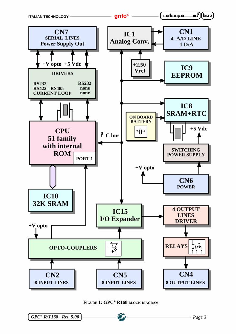
GPC® R168 and GPC® T168 (General Purpose Controller Relays/Transistors 16 input, 8 output)boards are powerful low cost modules capable to work in autonomy as intelligent peripheralsand/or as remote controlled devices in a network of telecontrol and/or acquisition. They belong toM serie CPU cards, their size is 22.5x82x90 mm.GPC® R168 and GPC® T168 boards are provided with plastic container for direct mounting onstandard Omega rails type DIN 46277-1 and DIN 46277-3. Thanks to the low cost of this CPU serie,it is possible to successfully solve, also all those small automation problems, which have a limitedcost budget. Using the wide range of developing software tools, available for the GPC® R168 andGPC® T168 such as BASCOM 8051 or the very comfortable Intel MCS BASIC-52 to use in matchwith BXC51, and so on, it is possible to complete the applications in a very short time and withminimum investments. The cards are provided with comfortable connectors that simplify theconnection with field signals, requiring no further modules and further cost. Moreover theseconnectors reduce times when possible up date and assistance phases must be performed.
- ABACO® Block M Serie size 22.5x82x90 mm- Housing for Omega rail DIN 46277-1 and DIN 46277-3 types- Available in 3 different versions with the following CPUs:
GPC® R/T168 with Atmel 89C52 22MHz, 32K external SRAMGPC® R/T168A with Atmel 89S8252 22MHz; 8K internal FLASH; 2K
internal EEPROM; 32K external SRAMGPC® R/T168P with Philips 89C51Rx2 22MHz; from 16K to 64K internal
FLASH; from 512 bytes to 1K internal SRAM; 32K externalSRAM; serial ISP Flash programming through RS 232
- Total addressable memory is 96K divided in: 32K static RAM soldered; 64K Flash EPROMinside the microcontroller
- Code compatible with family 51 µP- Real Time Clock with 256 Byte of internal RAM- Back up circuitry for RTC and RAM, through LITHIUM battery- Real Time Clock output for /INT management or frequency output- 16 NPN digital input lines, galvanically isolated; 8 of them are connected to the microcontroller
and 8 are connected to PCF8575 that generates INT ad whenever inputs change- 8 output relays 5A- 4 A/D lines and one 8 bit D/A through PCF 8591- I/O connections through quick release screw terminal connectors- 3 timer counter resolution16 bits- Serial lines in RS232, or in RS422, RS485 or Current-Loop- Supply of the galvanically isolated section: +24 Vdc- Supply of the on board logic: 5Vdc or 10÷40 Vdc or 8÷24Vac- Supply protection through TransZorb™- Wide range of development software available like C compilers, Assembler, BXC51, MCS
BASIC 52, HTC 51, BASCOM 8051, PASCAL, CMX , etc.
The following pages describe each section of the card in a more detailed mode and figures 1 and 2illustrate the sections interconnections.
ITALIAN TECHNOLOGY grifo ®
Page 3 GPC® R/T168 Rel. 5.00
2CPU51 family
with internalROM
PORT 1
OPTO-COUPLERS
CN7SERIAL LINES
Power Supply Out
DRIVERS
RS232RS422 - RS485CURRENT LOOP
RS232nonenone
+V opto
IC1032K SRAM
+V opto +5 Vdc
FIGURE 1: GPC® R168 BLOCK DIAGRAM
IC9EEPROM
I C bus
IC8SRAM+RTC
CN14 A/D LINE
1 D/A
CN6POWER
SWITCHINGPOWER SUPPLY
+5 Vdc
CN28 INPUT LINES
CN48 OUTPUT LINES
4 OUTPUT LINES
DRIVER
RELAYS
+ -
ON BOARDBATTERY
+V opto
CN58 INPUT LINES
+2.50 Vref
IC15I/O Expander
IC1Analog Conv.

grifo ® ITALIAN TECHNOLOGY
Page 4 GPC® R/T168 Rel. 5.00
CPU
The GPC® R/T168 are designed to use all the microprocessors characterized by a family 51compliant pin out. Such 8 bit microprocessors are provided with an internal FLASH EPROM sizedat least 8 KBytes up to 64 KBytes, are widely diffused all over the world and have an extendedinstruction set, fast execution time,fast data handling,an efficient interrupt management, severalhardware peripherals integrated.Here follows a list of the main features of these CPU's:
- µP AT89C52 manufactured by ATMEL:- 12 clock pulses per machine cycle;- 256 bytes internal SRAM;- 8 KBytes internal FLASH EPROM;- 2 interrupt priority levels and 6 interrupt sources;- 1 synchronous/asynchronous serial line;
- µP AT89S8252 manufactured by ATMEL:- 12 clock pulses per machine cycle;- 256 bytes internal SRAM;- 8 KBytes internal FLASH EPROM;- 2 KBytes internal EEPROM;- 2 interrupt priority levels and 6 interrupt sources;- 1 synchronous/asynchronous serial line;
- µP AT89C51RB2/ RC2/ RD2 manufactured by PHILIPS:- 6 or12 clocks system cycle;- 16K/32K/64K Bytes internal FLASH EPROM;- 512 or 1K Bytes internal SRAM;- 4 interrupt priority levels and 7 interrupt sources;- 1 syncronous/asyncronous serial line;- ISP and IAP programming;
By default, GPC® R/T168 are provided with AT89C52.For further information on the listed microprocessor, please refer to specific documentation of themanufacturing company.
POWER SUPPLY
One of the most important features of GPC® R/T168 is its on board power supply circuitery; the cardcan be powered in two different ways: +5 Vdc (without power supply section) or 10÷24Vac(switching section). The power supply circuit generates the necessary voltages for the card, startingfrom all the standard industrial source like mains, power transformer, battery, solar cell, etc. The Usermust provide also a 24 Vdc voltage for the optocoupled section. The power supply type must bespecified at the moment of the order. The power supply circuit was designed for reducing theconsumption (the microprocessor power down and idle mode is available) and for increasing theelectrical noise immunity.Remember that on board there is a protection circuit aganist voltage peaks by TransZorb™.

ITALIAN TECHNOLOGY grifo ®
Page 5 GPC® R/T168 Rel. 5.00
OPTO-COUPLERS
CN7SERIAL LINES
Power Supply Out
DRIVERS
RS232RS422 - RS485CURRENT LOOP
RS232nonenone
+V opto
CPU51 family
with internalROM
PORT 1
+V opto +5 Vdc
IC1032K SRAM
FIGURE 2: GPC® T168 BLOCK DIAGRAM
IC9EEPROM
I C bus2
IC8SRAM+RTC
CN14 A/D LINE
1 D/A
CN6POWER
SWITCHINGPOWER SUPPLY
+5 Vdc
CN28 INPUT LINES
CN48 OUTPUT LINES
+ -
ON BOARDBATTERY
+V opto
CN58 INPUT LINES
+2.50 Vref
IC15I/O Expander
IC1Analog Conv.
OPTOCOUPLERS
OPENCOLLECTORTRANSISTORS
grifo ® ITALIAN TECHNOLOGY
Page 6 GPC® R/T168 Rel. 5.00
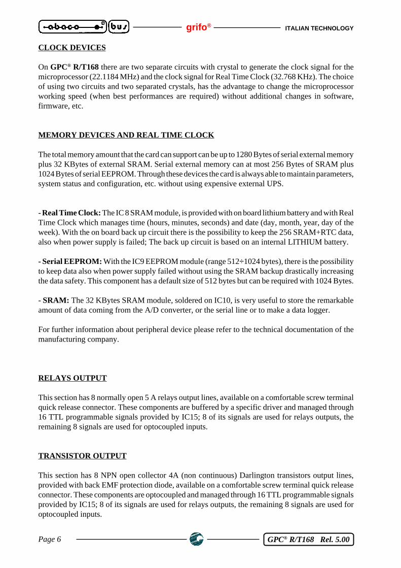
CLOCK DEVICES
On GPC® R/T168 there are two separate circuits with crystal to generate the clock signal for themicroprocessor (22.1184 MHz) and the clock signal for Real Time Clock (32.768 KHz). The choiceof using two circuits and two separated crystals, has the advantage to change the microprocessorworking speed (when best performances are required) without additional changes in software,firmware, etc.
MEMORY DEVICES AND REAL TIME CLOCK
The total memory amount that the card can support can be up to 1280 Bytes of serial external memoryplus 32 KBytes of external SRAM. Serial external memory can at most 256 Bytes of SRAM plus1024 Bytes of serial EEPROM. Through these devices the card is always able to maintain parameters,system status and configuration, etc. without using expensive external UPS.
- Real Time Clock: The IC 8 SRAM module, is provided with on board lithium battery and with RealTime Clock which manages time (hours, minutes, seconds) and date (day, month, year, day of theweek). With the on board back up circuit there is the possibility to keep the 256 SRAM+RTC data,also when power supply is failed; The back up circuit is based on an internal LITHIUM battery.
- Serial EEPROM: With the IC9 EEPROM module (range 512÷1024 bytes), there is the possibilityto keep data also when power supply failed without using the SRAM backup drastically increasingthe data safety. This component has a default size of 512 bytes but can be required with 1024 Bytes.
- SRAM: The 32 KBytes SRAM module, soldered on IC10, is very useful to store the remarkableamount of data coming from the A/D converter, or the serial line or to make a data logger.
For further information about peripheral device please refer to the technical documentation of themanufacturing company.
RELAYS OUTPUT
This section has 8 normally open 5 A relays output lines, available on a comfortable screw terminalquick release connector. These components are buffered by a specific driver and managed through16 TTL programmable signals provided by IC15; 8 of its signals are used for relays outputs, theremaining 8 signals are used for optocoupled inputs.
TRANSISTOR OUTPUT
This section has 8 NPN open collector 4A (non continuous) Darlington transistors output lines,provided with back EMF protection diode, available on a comfortable screw terminal quick releaseconnector. These components are optocoupled and managed through 16 TTL programmable signalsprovided by IC15; 8 of its signals are used for relays outputs, the remaining 8 signals are used foroptocoupled inputs.
ITALIAN TECHNOLOGY grifo ®
Page 7 GPC® R/T168 Rel. 5.00
INPUT SECTION
GPC® R/T168 cards are provided with 16 NPN optocoupled inputs; 8 inputs are acquired directlyby the microprocessor (Port 1), the remaining 8 inputs are acquired through PCF8575 soldered onIC15 and implementing a serial protocol. This device is capable to trigger an interrupt whenever oneif its inputs changes, this allows the microprocessor to save time because it must not poll countinuoslythese 8 signals, it is enough to wait for the interrupt.The inputs are available on a comfortable screw terminal quick release connector.
A/D AND D/A CONVERTER
GPC® R/T168 cards are provided with a A/D and D/A converter, implemented through IC1: thisperipheral is capable to acquire 4 channels and to drive 1 channel with a maximum resolution of 8bits.By software it is possible to decide wich channel to activate through I 2C-BUS serialcommunication. The analog signals connectable are in the range 0÷2.5V.
SERIAL COMMUNICATION SELECTION
GPC® R/T168 cards are provided with two serial lines, one software and one hardware completelysoftware settable, both as communication protocol and speed. These settings are performed byprogramming on board microprocessor's internal registers, so for further information please refer tomanufacturers documentation.By hardware the two serial lines can work only as RS 232. Other communication protocols can beimplemented only by the hardware serial line losing the possibility to use the software serial line.Other protocols implementable are current loop, RS 485 and RS 422, in this latter case thecommunication can be implemented as Full Duplex or Half Duplex.

grifo ® ITALIAN TECHNOLOGY
Page 8 GPC® R/T168 Rel. 5.00
GPCGPC®® R168 TECHNICAL FEATURES R168 TECHNICAL FEATURES
GPC® R168 GENERAL FEATURES
On board resources: 16 NPN optocoupled digital inputs8 normally open 5 A relays digital outputs4 A/D converter signals1 D/A converter signal1 real time clock2 RS 232 serial lines or one RS 422-485 or Current Loop
Memory addressable: IC 8: serial 256 Bytes RTC+SRAMIC 9: serial EEPROM from 512 Bytes to 1 KBytesIC10: SRAM 32 KBytes
CPU: Atmel AT89C52 8 KBytes Flash-EpromAtmel AT89S8252 8 KBytes Flash-EpromPhilips P89C51RB2 16 KBytes Flash-EpromPhilips P89C51RC2 32 KBytes Flash-EpromPhilips P89C51RD2 64 Kbytes Flash-Eprom
CPU clock frequence: 22.1184 MHz
RTC clock frequence: 32.768 KHz
A/D converter general features:Resolution: 8 bitConversion time: 90 µsec
D/A converter general features:Resolution: 8 bitConversion time: 90 µsec
GPC® R168 PHYSICAL FEATURES
Size (W x H x D): 109 x 104 x 22.5 mm109 x 115 x 22.5 mm (included container for Ω rails)
Mounting: Ω rails type DIN 46277-1 and DIN 46277-3
Weight: 196 g (basic version)
Connectors: CN1: 7 pins quick release 90° pitch 3.5 mmCN2: 9 pins quick release 90° pitch 3.5 mmCN4: 11 pins quick release 90° pitch 5 mmCN5: 9 pins quick release 90° pitch 3.5 mmCN6: 4 pins quick release 90° pitch 3.5 mmCN7: 4+4 pins AMP Mod II 90°
ITALIAN TECHNOLOGY grifo ®
Page 9 GPC® R/T168 Rel. 5.00
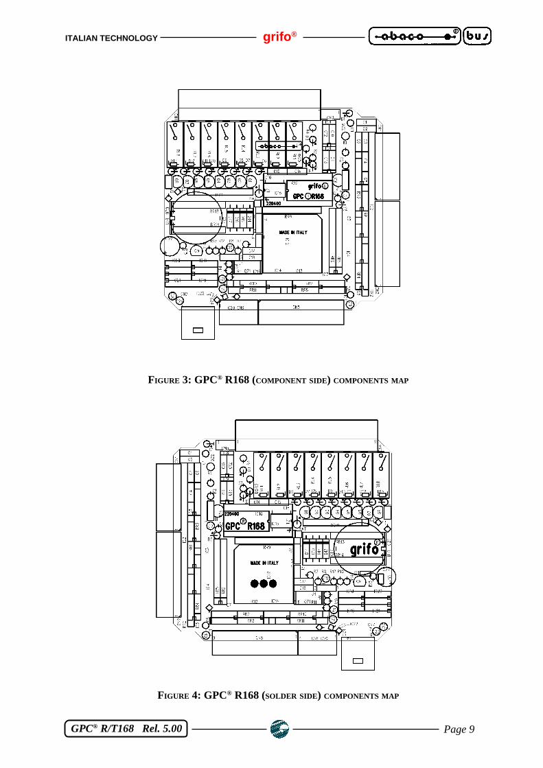
FIGURE 3: GPC® R168 (COMPONENT SIDE) COMPONENTS MAP
FIGURE 4: GPC® R168 (SOLDER SIDE) COMPONENTS MAP
grifo ® ITALIAN TECHNOLOGY
Page 10 GPC® R/T168 Rel. 5.00
Temperature range: from 0 to 50 Centigrad degreeses
Relative humidity: 20% up to 90% (without condensing)
GPC® R168 ELECTRIC FEATURES
Version without power supplyPower supply voltage: +5 Vdc (control logic)
+24 Vdc (+V opto)
Version with switching power supplyInput power supply voltage: 10÷40 Vdc o 8÷24 Vac (control logic)
24 Vdc (+V opto)
Output power supply voltage: +5 Vdc; 550 mA+Vopto 100 mA
Current consumption: 450 mA max (+5 Vdc)37 mA max (+V opto)
Relays maximum current: 5A
Relays maximum voltage: 30 Vdc / 250 Vac
NPN inputs minimum current: 1 mA
Back up current: 3,5 µA
On board back up battery: 3 V; 180 mAh; mod. CR 2032
A/D converter electric features:Voltage range: 0÷2.5VdcInput impedance: not specified
D/A converter electric features:Voltage range: 0÷2.5VdcLoad acceptable: 10K
RS422-485 termination network: Line termination resistor = 120 ΩPositive pull up resistor = 3,3 KΩNegative pull down resistor = 3,3 KΩ
ITALIAN TECHNOLOGY grifo ®
Page 11 GPC® R/T168 Rel. 5.00
GPCGPC®® T168 TECHNICAL FEATURES T168 TECHNICAL FEATURES
GPC® T168 GENERAL FEATURES
On board resources: 16 NPN optocoupled digital inputs8 open collector darlington NPN transistors digital outputs, with back EMF protection diode4 A/D converter signals1 D/A converter signal1 real time clock2 RS 232 serial lines or one RS 422-485 or Current Loop
Memory addressable: IC 8: serial 256 Bytes RTC+SRAMIC 9: serial EEPROM from 512 Bytes to 1 KBytesIC10: SRAM 32 KBytes
CPU: Atmel AT89C52 8 KBytes Flash-EpromAtmel AT89S8252 8 KBytes Flash-EpromPhilips P89C51RB2 16 KBytes Flash-EpromPhilips P89C51RC2 32 KBytes Flash-EpromPhilips P89C51RD2 64 Kbytes Flash-Eprom
CPU clock frequence: 22.1184 MHz
RTC clock frequence: 32.768 KHz
A/D converter general features:Resolution: 8 bitConversion time: 90 µsec
D/A converter general features:Resolution: 8 bitConversion time: 90 µsec
GPC® T168 PHYSICAL FEATURES
Size (W x H x D): 109 x 104 x 22.5 mm109 x 115 x 22.5 mm (included container for Ω rails)
Mounting: Ω rails type DIN 46277-1 and DIN 46277-3
Weight: 181 g (basic version)
Connectors: CN1: 7 pins quick release 90° pitch 3.5 mmCN2: 9 pins quick release 90° pitch 3.5 mmCN4: 11 pins quick release 90° pitch 5 mmCN5: 9 pins quick release 90° pitch 3.5 mmCN6: 4 pins quick release 90° pitch 3.5 mmCN7: 4+4 pins AMP Mod II 90°
grifo ® ITALIAN TECHNOLOGY
Page 12 GPC® R/T168 Rel. 5.00
Temperature range: from 0 to 50 Centigrad degreeses
Relative humidity: 20% up to 90% (without condensing)
GPC® T168 ELECTRIC FEATURES
Version without power supplyPower supply voltage: +5 Vdc (control logic)
+24 Vdc (+V opto)
Version with switching power supplyInput power supply voltage: 10÷40 Vdc o 8÷24 Vac (control logic)
24 Vdc (+V opto)
Output power supply voltage: +5 Vdc; 550 mA+Vopto 100 mA
Current consumption: 106 mA max (+5 Vdc)37 mA max (+V opto)
Transistors maximum current: 4A (not contiguous) (*)
Transistors maximum voltage: 45 Vdc (*)
Transistors maximum power: 1.25 W (*)
NPN inputs minimum current: 1 mA
Back up current: 3,5 µA
On board back up battery: 3 V; 180 mAh; mod. CR 2032
A/D converter electric features:Voltage range: 0÷2.5VdcInput impedance: not specified
D/A converter electric features:Voltage range: 0÷2.5VdcLoad acceptable: 10K
RS422-485 termination network: Line termination resistor = 120 ΩPositive pull up resistor = 3,3 KΩNegative pull down resistor = 3,3 KΩ
(*) These values are referred to a working temperature of 20 °C

ITALIAN TECHNOLOGY grifo ®
Page 13 GPC® R/T168 Rel. 5.00
FIGURE 5: GPC® T168 (COMPONENT SIDE) COMPONENTS MAP
FIGURE 6: GPC® T168 (SOLDER SIDE) COMPONENTS MAP

grifo ® ITALIAN TECHNOLOGY
Page 14 GPC® R/T168 Rel. 5.00
INSTALLATIONINSTALLATION
In this chapter there are the information for a right installation and correct use of the card. The Usercan find the location and functions of each connector, jumper installed on GPC® R/T168 and someexplanatory diagrams.
CONNECTIONS
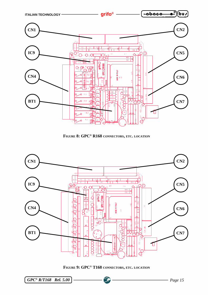
The GPC® R/T168 modules have 6 connectors that can be linked to other devices or directly to thefield, according to system requirements. In this paragraph there are connectors pin out, a short signalsdescription (including the signals direction) and connectors location. To easily locate them pleaserefer to figures 8 and 9, while for further information about the connections please refer to thefollowing figures.
CN6 - POWER SUPPLY CONNECTOR
CN6 is a 4 pins, quick release, screw terminal connector 3.5 mm pitch. CN6 is used to power the cardwhen on GPC® R168 or GPC® T168 there is the switching power supply section and to supply theoptocouplers.Please remark that for a correct working of the board these two tension must be galvanically isolaed.
FIGURE 7: CN6 - POWER SUPPLY CONNETTOR
Signals description:
+V opto = I - +V opto power supply.GND opto = - +V opto ground signal.Vac = I - Control logic power supply line (+10÷40 Vdc or 10÷24Vac).Vac = I - Control logic power supply line (+10÷40 Vdc or 10÷24Va)c.
For further information please refer to the paragraph “POWER SUPPLY VOLTAGES”
1
2
3
4Vac
Vac
+V opto
GND opto
ITALIAN TECHNOLOGY grifo ®
Page 15 GPC® R/T168 Rel. 5.00
FIGURE 8: GPC® R168 CONNECTORS, ETC. LOCATION
FIGURE 9: GPC® T168 CONNECTORS, ETC. LOCATION
CN1
IC9
BT1
CN2
CN6
CN5
CN4
CN7
CN1
IC9
BT1
CN2
CN6
CN5
CN4
CN7

grifo ® ITALIAN TECHNOLOGY
Page 16 GPC® R/T168 Rel. 5.00
CN7 - POWER SUPPLY AND SERIAL LINES CONNECTOR
CN7 is a 4+4 pins AMP Mod II type connector with 2.54 mm pitch.If the GPC® R168 or GPC® T168 has the switching power section mounted, trough CN7 the usercan draw the two galvanically isolated voltages and can use them for external loads supply.In the other case (switching not present) trough CN7 the user must give the two voltages (+5 Vdc and+Vopto) for card power supply. Also, on CN7 connector are available the buffered signals for RS232, RS 422, RS 485 or Current Loop serial line communication, all CCITT normatives compliant.All the signals are placed in order to reduce interference and electrical noise. The female connectorcan be ordered directly to grifo ® (code CKS.AMP8) or to AMP (connector P/N: 280365; pins asloose pieces P/N:182206-2).
FIGURE 10: CN7 - POWER SUPPLY AND SERIAL LINES CONNECTOR
Signals description:
RxDA/B RS 232= I - Receive Data of RS 232 serial line.TxDA/B RS 232= O - Transmit Data of RS 232 serial line.RX- RS 422 = I - Receive Data Negative of RS 422 serial line.RX+ RS 422 = I - Receive Data Positive of RS 422 serial line.TX- RS 422 = O - Transmit Data Negativ of RS 422 serial line.TX+ RS 422 = O - Transmit Data Positive of RS 422 serial line.TXRX- RS 485 = I/O - Transmit Receive Data Negative of RS 485 serial line.TXRX+ RS 485 = I/O - Transmit Receive Data Positive of RS 485 serial line.RX- C.L. = I - Receive Data Negative of Current Loop serial line.RX+ C.L. = I - Receive Data Positive of Current Loop serial line.TX- C.L. = O - Transmit Data Negative of Current Loop serial line.TX+ C.L. = O - Transmit Data Positive of Current Loop serial line.+5 Vdc = I/O - Positive terminal of +5 Vdc power supply.GND = - +5 Vdc ground.+V opto = I/O - Positive terminal of +V opto power supply.GND opto = - +V opto ground.
1 2
3 4
5 6
7 8GND
TxDA RS 232 / TX- RS422 / TX- C.L.
RxDA RS232 / RX+ RS422 / TXRX+ RS485 / RX+ C.L. RxDB RS232 / RX- RS422 / TXRX- RS485 / RX- C.L.
TxDB RS 232 / TX+ RS422 / TX+ C.L.
+5 Vdc
GND opto
+Vopto
ITALIAN TECHNOLOGY grifo ®
Page 17 GPC® R/T168 Rel. 5.00
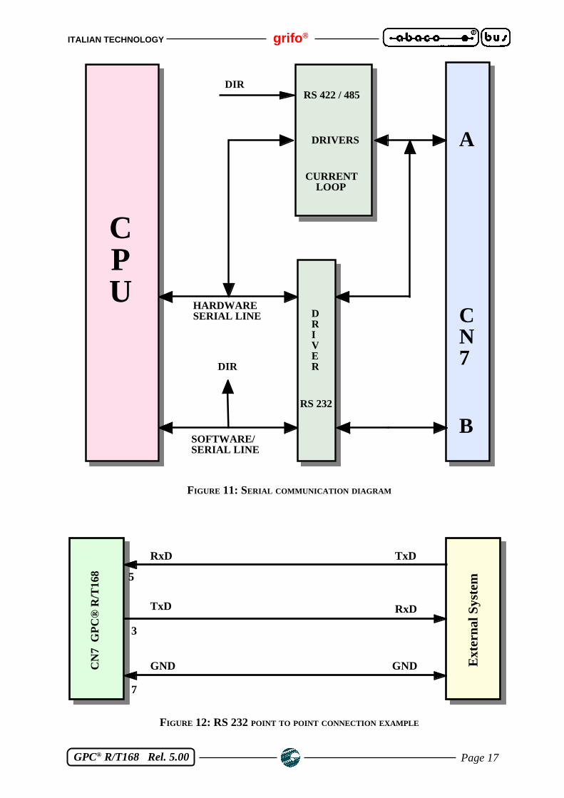
FIGURE 11: SERIAL COMMUNICATION DIAGRAM
FIGURE 12: RS 232 POINT TO POINT CONNECTION EXAMPLE
CPU
DRIVER
RS 232
DRIVERS
RS 422 / 485
CURRENTLOOP
DIR
CN7
SOFTWARE/SERIAL LINE
HARDWARESERIAL LINE
DIR
A
B
5
3
7
RxD
TxD
GND GND
RxD
TxD
Ext
erna
l Sys
tem
CN
7 G
PC
® R
/T16
8

grifo ® ITALIAN TECHNOLOGY
Page 18 GPC® R/T168 Rel. 5.00
FIGURE 13: RS 422 POINT TO POINT CONNECTION EXAMPLE
FIGURE 14: RS 485 POINT TO POINT CONNECTION EXAMPLE
NOTEThere can be two serial lines, one software and one hardware, only in RS 232, in all other cases thereis only one serial line.
6
5
7
RX -
RX +
GND GND
TX +
TX -
Ext
erna
l Sys
tem
CN
7 G
PC
® R
/T16
8
3
4
TX -
TX + RX +
RX -
6
5
7
TXRX -
TXRX +
GND GND
RX / TX +
RX / TX -
Mas
ter
Rem
ote
Sys
tem
CN
7 G
PC
® R
/T16
8
ITALIAN TECHNOLOGY grifo ®
Page 19 GPC® R/T168 Rel. 5.00
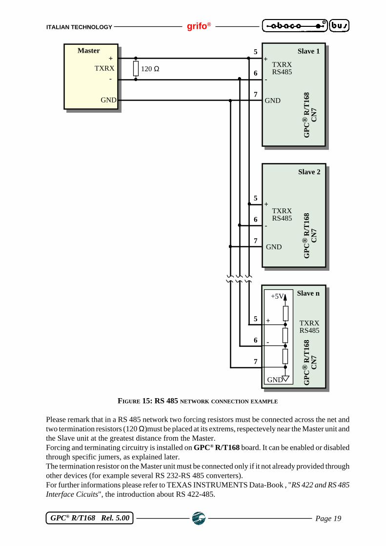
FIGURE 15: RS 485 NETWORK CONNECTION EXAMPLE
Please remark that in a RS 485 network two forcing resistors must be connected across the net andtwo termination resistors (120 Ω)must be placed at its extrems, respectevely near the Master unit andthe Slave unit at the greatest distance from the Master.Forcing and terminating circuitry is installed on GPC® R/T168 board. It can be enabled or disabledthrough specific jumers, as explained later.The termination resistor on the Master unit must be connected only if it not already provided throughother devices (for example several RS 232-RS 485 converters).For further informations please refer to TEXAS INSTRUMENTS Data-Book , "RS 422 and RS 485Interface Cicuits", the introduction about RS 422-485.
TXRX +
-
GND
Master
120 Ω
+
-
Slave n
GND
+5V
+
-
GND
Slave 2
TXRXRS485
+
-
GND
Slave 1
GP
C®
R/T
168
CN
7G
PC
® R
/T16
8C
N7
GP
C®
R/T
168
CN
7
TXRXRS485
TXRXRS485
7
6
5
7
6
5
7
6
5

grifo ® ITALIAN TECHNOLOGY
Page 20 GPC® R/T168 Rel. 5.00
FIGURE 16: 4 WIRES CURRENT LOOP POINT TO POINT CONNECTION EXAMPLE
FIGURE 17: 2 WIRES CURRENT LOOP POINT TO POINT CONNECTION EXAMPLE
6
5
RX -
RX + TX -
TX +
Ext
erna
l Sys
tem
CN
7 G
PC
® R
/T16
8
3
4
TX -
TX + RX -
RX +
- +VCL
R
R
6
5
RX -
RX + TX -
TX +E
xter
nal S
yste
m
CN
7 G
PC
® R
/T16
8
3
4
TX -
TX + RX -
RX +
- +VCL
R

ITALIAN TECHNOLOGY grifo ®
Page 21 GPC® R/T168 Rel. 5.00
FIGURE 18: PASSIVE CURRENT LOOP NETWORK CONNECTION EXAMPLE
Possible Current Loop connections are two: 2 wires and 4 wires. These connections are shown infigures 17 and 18 where it is possible to see the voltage for VCL and the resistances for currentlimitation (R). The supply voltage varies in compliance with the number of connected devices andvoltage drop on the connection cable.The choice of the values for these components must be done cosidering that:- circulation of a 20 mA current must be guaranteed;- potential drop on each transmitter is about 2.35 V with a 20 mA current;- potential drop on each receiver is about 2.52 V with a 20 mA current;- in case of shortciruit each transmitter must dissipate at most 125 mW;- in case of shortciruit each receiver must dissipate at most 90 mW.For further info please refer to HEWLETT-PACKARD Data Book, (HCPL 4100 and 4200 devices).
TX +
-
Master
Slave n
Slave 2
RX+
-
Slave 1
GPC® R/T168
RX +
-
6
5
3
4
-+ VCL
R
R
TX+
-
RX+
-
TX+
-
RX+
-
TX+
-
CN7
CN7
CN7
6
5
3
4
6
5
3
4
GPC® R/T168
GPC® R/T168

grifo ® ITALIAN TECHNOLOGY
Page 22 GPC® R/T168 Rel. 5.00
CN2 - CONNECTOR FOR OPTOCOUPLED INPUTS
CN2 is a 9 pins, quick release, screw terminal connector.CN2 is used to connect the 8 out of 16 optocoupled NPN input signals that the CPU manages directlythrough port 1.On the connector is also available the optocoupled inputs power supply ground signal.
FIGURE 19: CN2 - CONNECTOR FOR OPTOCOUPLED INPUTS
Signals description:
P1.0÷P1.7 = I - Open collector NPN input, connected to CPU port 1 pins.GND opto = - Opto ground.
1
2
3
4
5
6
7
8
9
P1.0
P1.1
P1.2
P1.3
P1.4
P1.6
P1.7
GND opto
P1.5
ITALIAN TECHNOLOGY grifo ®
Page 23 GPC® R/T168 Rel. 5.00
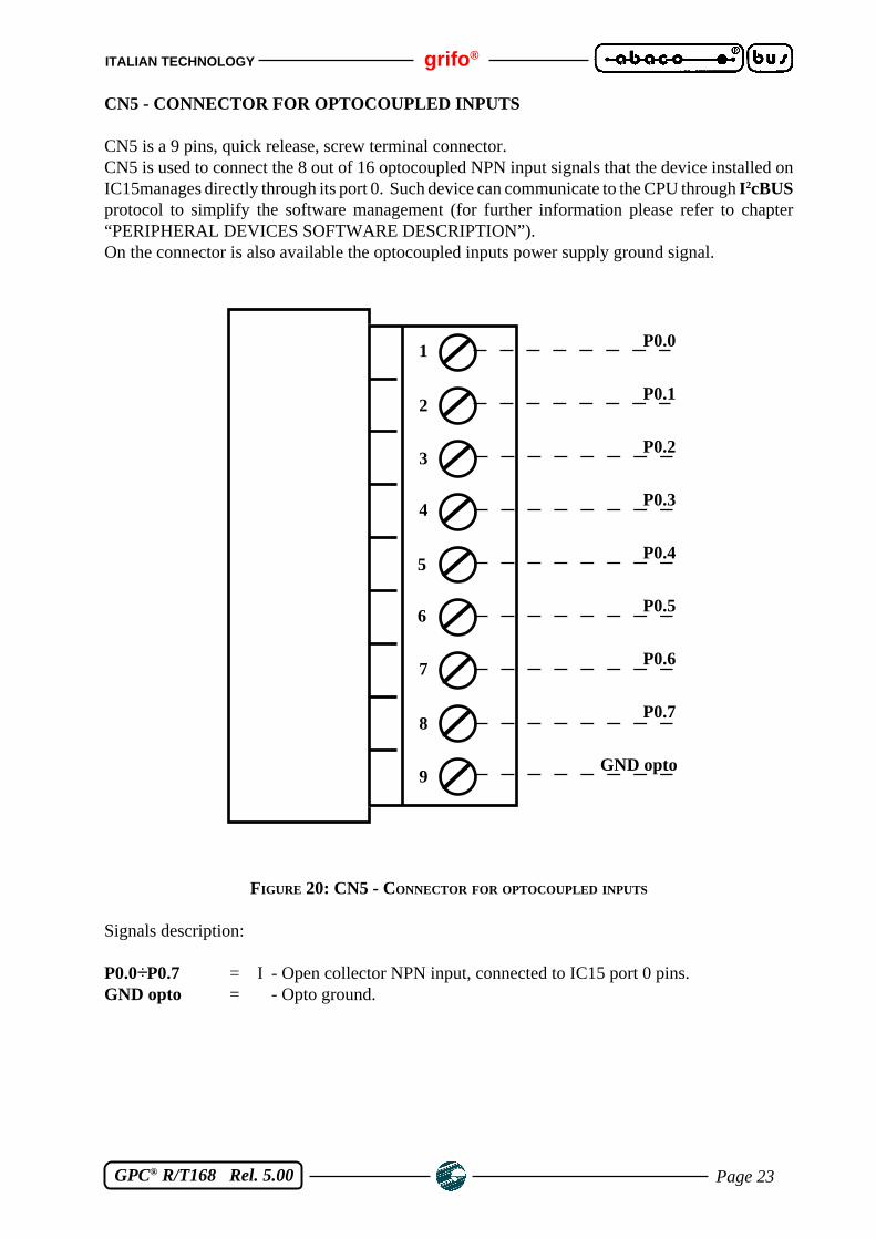
CN5 - CONNECTOR FOR OPTOCOUPLED INPUTS
CN5 is a 9 pins, quick release, screw terminal connector.CN5 is used to connect the 8 out of 16 optocoupled NPN input signals that the device installed onIC15manages directly through its port 0. Such device can communicate to the CPU through I 2cBUSprotocol to simplify the software management (for further information please refer to chapter“PERIPHERAL DEVICES SOFTWARE DESCRIPTION”).On the connector is also available the optocoupled inputs power supply ground signal.
FIGURE 20: CN5 - CONNECTOR FOR OPTOCOUPLED INPUTS
Signals description:
P0.0÷P0.7 = I - Open collector NPN input, connected to IC15 port 0 pins.GND opto = - Opto ground.
1
2
3
4
5
6
7
8
9
P0.0
P0.1
P0.2
P0.3
P0.4
P0.6
P0.7
GND opto
P0.5

grifo ® ITALIAN TECHNOLOGY
Page 24 GPC® R/T168 Rel. 5.00
The inputs available on the board are optocoupled, provided with a low-pass filter to warrant a certaindegree of internal electronic protection against noise coming from external world. The inputs aresuitable for NPN type drivers, to connect them to PNP drivers yuo should interpose a PBI 01 module.The 9 inputs section circuitery is shown in the diagram below.Optocouplers power supply may be granted by connector CN6.
FIGURE 21: OPTOCOUPLED INPUTS BLOCK DIAGRAM
POWER
SUPPLYC
N2,
CN
5
PO
TE
NT
IAL
DIV
IDE
R B
Y
RE
SIS
TO
RS
PIN
9P
IN 1
÷8
GND opto
+Vopto
OP
TO
-CO
UP
LER
S
8 NPN Input lines
Por
t 1 C
PU
, Por
t 0 IC
15 P
CF
8575
ITALIAN TECHNOLOGY grifo ®
Page 25 GPC® R/T168 Rel. 5.00
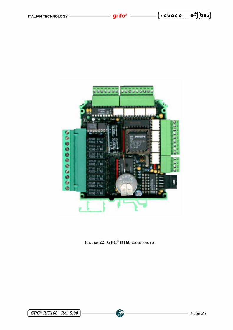
FIGURE 22: GPC® R168 CARD PHOTO

grifo ® ITALIAN TECHNOLOGY
Page 26 GPC® R/T168 Rel. 5.00
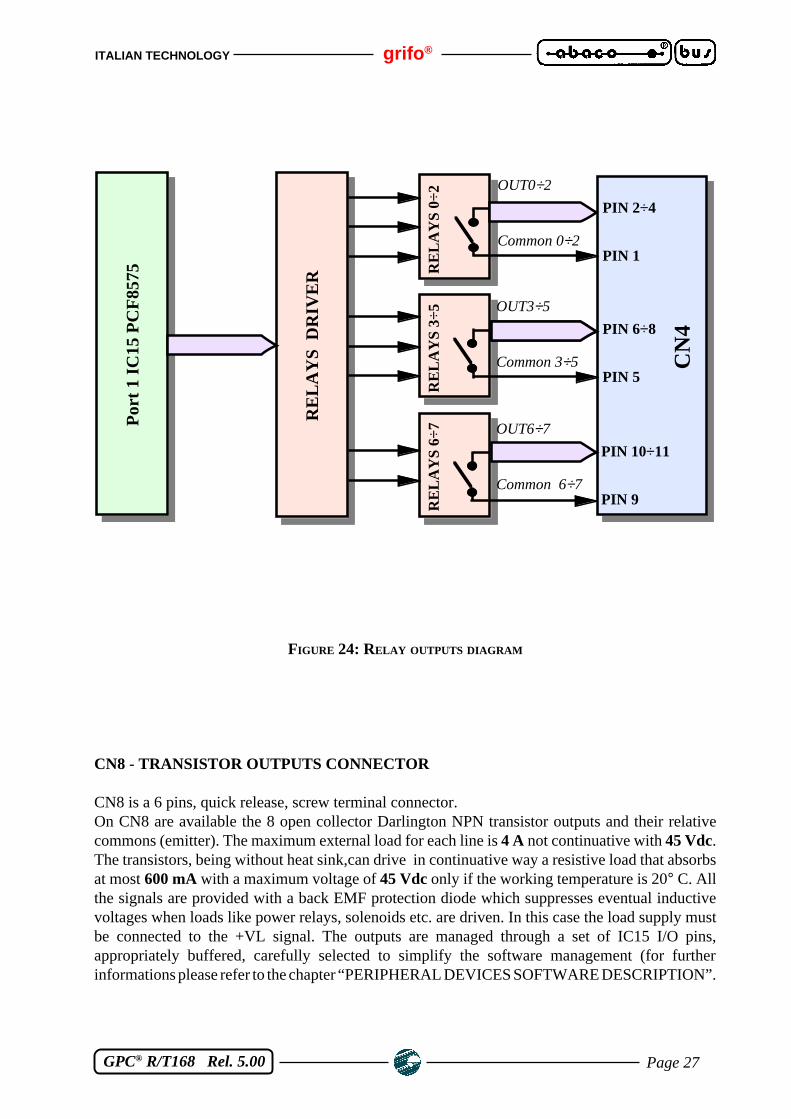
CN4 - RELAY OUTPUTS CONNECTOR
CN4 is a 11 pins, quick release screw terminal connector. On CN4 are available the normally open8 relays outputs and their relative commons. The maximum external load for each line is 5 A witha maximum tension or 30 Vdc or 250 Vac.The outputs are managed through port 1 of IC15, opportunaly buffered, carefully selected to simplifythe software management (for further information please refer to the chapter “PERIPHERALDEVICES SOFTWARE DESCRIPTION”).
FIGURE 23: CN4 - RELAY OUTPUTS CONNECTOR
Signals description:
NO OUT n (P1.x) = O - n-th relay normally open contact, driven through pin P1.x of device installed on IC15.
COMMON n (m ÷p) = - Common contacts of the relays from m to p.
The relays are driven through 8 PNP transistrors that are driven through pins of the device installedon IC15.
1
2
3
4
5
6
7
8
9
10
11
COMMON 1 (0÷2)
NO OUT0
NO OUT1
NO OUT2
COMMON 2 (3÷5)
NO OUT4
NO OUT5
COMMON 3 (6÷7)
NO OUT6
NO OUT7
NO OUT3
ITALIAN TECHNOLOGY grifo ®
Page 27 GPC® R/T168 Rel. 5.00
FIGURE 24: RELAY OUTPUTS DIAGRAM
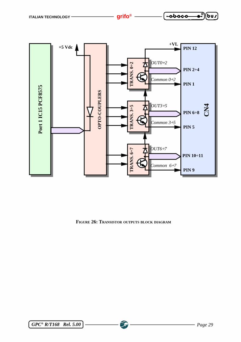
CN8 - TRANSISTOR OUTPUTS CONNECTOR
CN8 is a 6 pins, quick release, screw terminal connector.On CN8 are available the 8 open collector Darlington NPN transistor outputs and their relativecommons (emitter). The maximum external load for each line is 4 A not continuative with 45 Vdc.The transistors, being without heat sink,can drive in continuative way a resistive load that absorbsat most 600 mA with a maximum voltage of 45 Vdc only if the working temperature is 20° C. Allthe signals are provided with a back EMF protection diode which suppresses eventual inductivevoltages when loads like power relays, solenoids etc. are driven. In this case the load supply mustbe connected to the +VL signal. The outputs are managed through a set of IC15 I/O pins,appropriately buffered, carefully selected to simplify the software management (for furtherinformations please refer to the chapter “PERIPHERAL DEVICES SOFTWARE DESCRIPTION”.
CN
4
Por
t 1 IC
15 P
CF
8575
PIN 2÷4
OUT0÷2
RE
LAY
S 0
÷2
Common 0÷2PIN 1
RE
LAY
S D
RIV
ER
PIN 6÷8
OUT3÷5
Common 3÷5PIN 5
RE
LAY
S 3
÷5PIN 10÷11
OUT6÷7
Common 6÷7PIN 9R
ELA
YS
6÷7

grifo ® ITALIAN TECHNOLOGY
Page 28 GPC® R/T168 Rel. 5.00
FIGURE 25: CN4 - TRANSISTOR OUTPUTS CONNECTOR
Signals description:
OC OUT n (P1.x) = O -Open collector contact of n-th NPN transistor, driven by pin P1.x of device installed on IC15.
COMMON n (m ÷p) = - Common emitter of transistors from m to p..+VL = I - Back EMF protection diodes power supply (power supply of load).
Each transistor output line is optocoupled to warrant a great isolation between internal electronicsand the external world.The final stage of such outputs is made by an NPN Darlington transistor in Open Collector providedwith back EMF protection diode, the emitters are connected in groups of three, three and twoelements, allowing to connect up to three different tensions to be driven.
1
2
3
4
5
6
7
8
9
10
COMMON 1 (0÷2)
OC OUT0
OC OUT1
OC OUT2
COMMON 2 (3÷5)
OC OUT4
OC OUT5
COMMON 3 (6÷7)
OC OUT6
11OC OUT7
OC OUT3
12+VL
ITALIAN TECHNOLOGY grifo ®
Page 29 GPC® R/T168 Rel. 5.00
FIGURE 26: TRANSISTOR OUTPUTS BLOCK DIAGRAM
CN
4
TR
AN
S. 0
÷2
PIN 2÷4
OUT0÷2
Common 0÷2PIN 1
TR
AN
S. 6
÷7
PIN 10÷11
OUT6÷7
Common 6÷7PIN 9
OP
TO
-CO
UP
LER
S
+VLPIN 12+5 Vdc
TR
AN
S. 3
÷5
PIN 6÷8
OUT3÷5
Common 3÷5PIN 5
Por
t 1 IC
15 P
CF
8575

grifo ® ITALIAN TECHNOLOGY
Page 30 GPC® R/T168 Rel. 5.00
CN1 - A/D AND D/A CONVERTER CONNECTOR
CN1 is a 7 pins screw terminal quick release connector.CN1 allows to connect the analog signals available on GPC® R/T168 (4 input signals for the A/Dconverter, one output signal for the D/A converter and two power supply lines for eventual externalloads). The conversion management is performed by reading the analog converter registersconnected to the microprocessor through I 2cBUS as described in the chapter “PERIPHERALDEVICES SOFTWARE DESCRIPTION”.
FIGURE 27: CN1 - A/D AND D/A CONVERTER CONNECTOR
Signals descrption:
CHx = I - x-th input signal of A/D converter.D/A = O - Analog output signal of D/A converter.+5 Vdc = O - +5 Vdc power supply.AGND = - Analog ground.
1
2
3
4
5
6
7
CH0
CH1
CH2
CH3
AGnd
D/A
+5Vdc

ITALIAN TECHNOLOGY grifo ®
Page 31 GPC® R/T168 Rel. 5.00
FIGURE 28: A/D INPUT AND D/A CONVERTER OUTPUT BLOCK DIAGRAM
+2,5VRef.
CN
1
IC1
PC
F85
91
CH3 pin 4
CH2 pin 3
CH1 pin 2
CH0 pin 1
D/A pin 15
AGND
pin 13
pin 7
pin 6
pin 1
pin 3
pin 4
pin 2
pin 5
+5Vdc

grifo ® ITALIAN TECHNOLOGY
Page 32 GPC® R/T168 Rel. 5.00
INTERRUPTS
A remarkable feature of GPC® R/T168 cards is the powerful interrupt management.Here follows a short description of which devices can geneate interrupts and their modalities; forfurther information about interrputs management please refer to the microprocessor data sheet.
- CPU peripherals -> Possible interrupt sources are: Timer/Counter 0÷2; serial lines 0, 1;external interrupts 0÷5; internal watch dog, ecc.In particular TIMER 2, available on PORT 1, connector CN2.
NOTE: for further information about these interrputs management please refer to the microprocessordata sheet.- On board sources -> Generate an interrupt on pin /INT0 (P3.2) of microcontroller (see
jumper J2). Interrupt sources are two; IC8 (RTC) that can feature aprogrammable time base and IC15 (I/O expander) that can send aninterrupt whenever one of its inputs changes.
- External sources -> On connector CN2 PORT 1 is available. It has several functions boundto TIMER 2.
BACK UP
On GPC® R/T168 is provided with a Lithium battery, called BT1, that keeps data on SRAM+RTCalso when power supply fails. With jumper J5 the User can connect or disconnect the Back Upwhenever it is needed, so the battery life time is increased. To easily locate the battery please referto figures 8 and 9.
I/O CONNECTION
To prevent possible connecting problems between GPC® R/T168 and the external systems, the Userhas to read carefully the previous paragraph information and he must follow these instrunctions:
- For RS 232, RS 422, RS 485 and current loop signals the user must follow the standard rules of eachone of these protocols;
- The analog input (A/D Converter ) must be connected to signals within the ranges: 0÷2.5 V. Please remark that such input, available on connector CN1, is provided with a low pass filter that warrants a greater stability of the signal acquired
- To the optocoupled input signals only the contacts to be acquired must be connected. Such contacts (relays, swithces; etc.) must connect or must not connect the input signal INx to GND opto. For logic signals correspondace, the open contact corresponds to logic state 1, while the closed contact corresponds to logic state 0. Correspondance is compliant to the NPN normative.

ITALIAN TECHNOLOGY grifo ®
Page 33 GPC® R/T168 Rel. 5.00
- The relays output signals, available only on GPC® R168, must be connected directly to the load to be driven (power relays, etc.). The boards provides the normally open contact, for which maximum current is 5A with a tension that can be as high as 30 Vdc or 250 Vac. To give the chance to drive different loads with different supplies, three different COMMON contacts are available, that connect three different groups of relays.
- The Darlington NPN output signals, available only on GPC® T168, must be connected directly to the load to be driven (power relays, etc.). The boards provides the Open Collector output line, for which maximum current is 4A not continuative with a tension that can be as high as +45 Vdc. The transistors, being without heat sink,can drive in continuative way a resistive load that absorbs at most 600 mA with a maximum voltage as high as 24 Vdc only if the work temperature is 20° C.
FIGURE 29: GPC® T168 CARD PHOTO
grifo ® ITALIAN TECHNOLOGY
Page 34 GPC® R/T168 Rel. 5.00
POWER SUPPLY
One of the most important features of GPC® R/T168 is its on board power supply circuitery; the cardcan be powered in two different ways to let the User solve easier the problem to supply the board inany working condition:
Without switching power supply (default):+V opto: Supplies the optocouplers of the board's input section; it must be +24 Vdc and must be
provided through pins 1 and 2 of CN6 or pins 2 and 8 of CN7.+5 Vdc: Supplies the control logic and the board's output section: it must be +5 Vdc ± 5% and must
be provided through pins 1 and 7 of CN7.
With switching power supply (option .SW):+V opto: Supplies the optocouplers of the board's input section; it must be +24 Vdc and must be
provided through pins 1 and 2 of CN6 or pins 2 and 8 of CN7.Vac: Supplies the control logic and the board's output section through the on board switching
power supply: it must be 10÷40 Vdc or 8÷24 Vac and must be provided through pins 3and 4 of CN6. The power supply circuit generates the necessary voltages for the card,starting from all the standard industrial source like mains, power transformer, battery,solar cell, etc. It is possible to supply external loads with the +5 Vdc tension availableon pins 1 and 7 of CN7.Please remark that the on board switching supply section is provided with its own diodebridge, so if the supply is continuous tension the ground digital signal (GND) doesn'thave the same potential of the ground signal available on CN6.
To warrant the maximum electrical noise immunity and so the correct board's functions, powersupply voltages must be galvanically isolated, to assure this condition even starting from mainssupply the power supply EXPS-2 can be ordered.
The power supply type must be specified at the moment of the order and can be installed only bygrifo
® technicians. The power supply circuit was designed for reducing the consumption (the
microprocessor power down and idle mode is available) and for increasing the electrical noiseimmunity. On board there is a protection circuit aganist voltage peaks by TransZorb™.
SOLDER JUMPERS
The default setting of the solder jumpers, named JSxx, is performed with a small track on the solderside, so if this setting must be changed, first cut the default connection track with a sharp cutter andthen connect the required position with a low power solder .
ITALIAN TECHNOLOGY grifo ®
Page 35 GPC® R/T168 Rel. 5.00
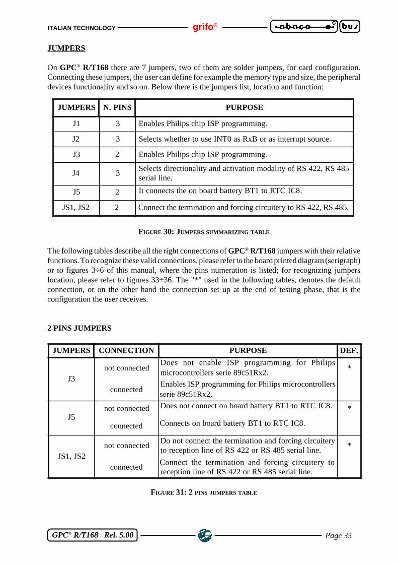
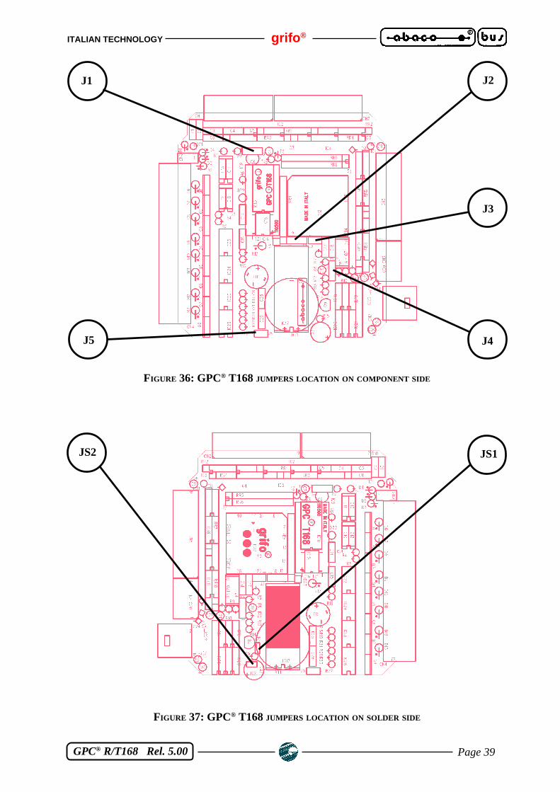
JUMPERS
On GPC® R/T168 there are 7 jumpers, two of them are solder jumpers, for card configuration.Connecting these jumpers, the user can define for example the memory type and size, the peripheraldevices functionality and so on. Below there is the jumpers list, location and function:
FIGURE 30: JUMPERS SUMMARIZING TABLE
The following tables describe all the right connections of GPC® R/T168 jumpers with their relativefunctions. To recognize these valid connections, please refer to the board printed diagram (serigraph)or to figures 3÷6 of this manual, where the pins numeration is listed; for recognizing jumperslocation, please refer to figures 33÷36. The "*" used in the following tables, denotes the defaultconnection, or on the other hand the connection set up at the end of testing phase, that is theconfiguration the user receives.
2 PINS JUMPERS
FIGURE 31: 2 PINS JUMPERS TABLE
JUMPERS N. PINS PURPOSE
J1 3 Enables Philips chip ISP programming.
J2 3 Selects whether to use INT0 as RxB or as interrupt source.
J3 2 Enables Philips chip ISP programming.
J4 3Selects directionality and activation modality of RS 422, RS 485serial line.
J5 2 It connects the on board battery BT1 to RTC IC8.
JS1, JS2 2 Connect the termination and forcing circuitery to RS 422, RS 485.
JUMPERS CONNECTION PURPOSE DEF.
J3not connected
Does not enable ISP programming for Philipsmicrocontrollers serie 89c51Rx2.
*
connectedEnables ISP programming for Philips microcontrollersserie 89c51Rx2.
J5not connected Does not connect on board battery BT1 to RTC IC8.*
connected Connects on board battery BT1 to RTC IC8.
JS1, JS2not connected
Do not connect the termination and forcing circuiteryto reception line of RS 422 or RS 485 serial line.
*
connectedConnect the termination and forcing circuitery toreception line of RS 422 or RS 485 serial line.

grifo ® ITALIAN TECHNOLOGY
Page 36 GPC® R/T168 Rel. 5.00
3 PINS JUMPERS
FIGURE 32: 3 PINS JUMPERS TABLE
FIGURE 33: GPC® R168 JUMPERS LOCATION ON COMPONENT SIDE
J1
J5
J2
J4
J3
JUMPERS CONNECTION PURPOSE DEF.
J1
position 1-2Enables ISP programming for Philipsmicrocontrollers serie 89c51Rx2.
position 2-3Does not enable ISP programming for Philipsmicrocontrollers serie 89c51Rx2.
*
J2position 1-2
Connects microcontroller INT0 pin to on boardinterrupt sources.
position 2-3 Connects INT0 to RxB of software serial. *
J4
position 1-2Selects serial line communication as RS 485 (2wires half duplex).
position 2-3Selects serial line communication as RS 422 (4wires full duplex or half duplex).
*
ITALIAN TECHNOLOGY grifo ®
Page 37 GPC® R/T168 Rel. 5.00
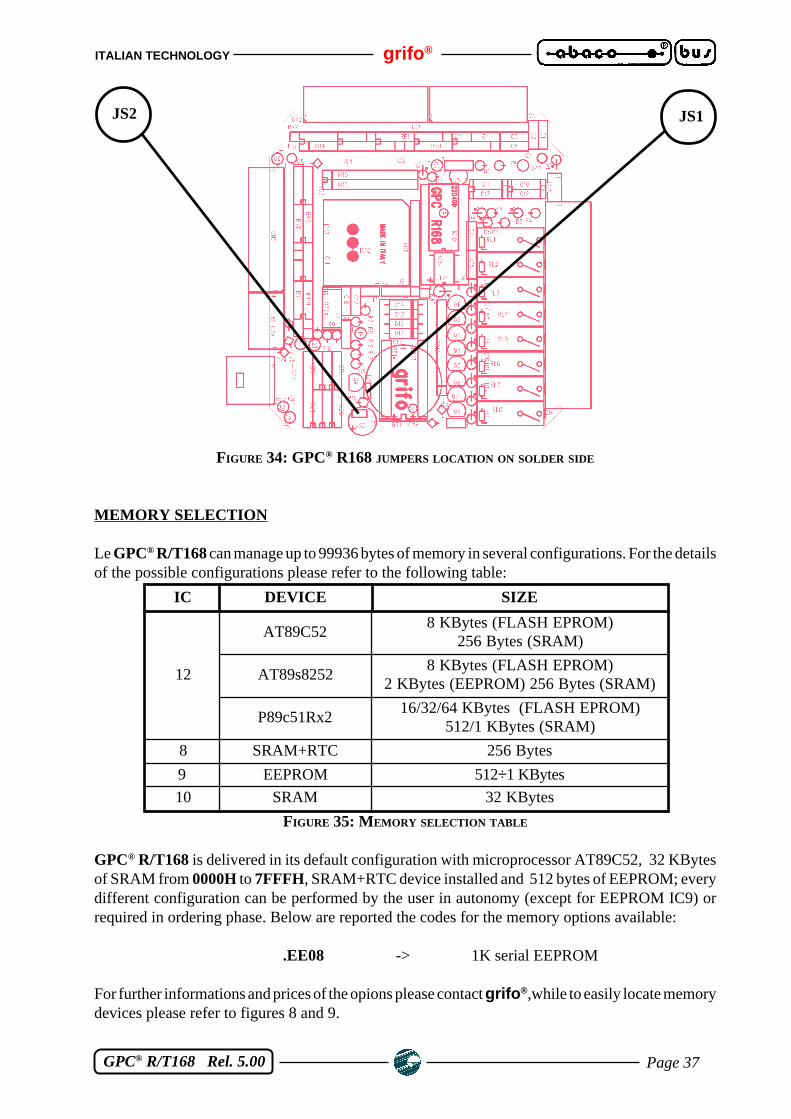
FIGURE 34: GPC® R168 JUMPERS LOCATION ON SOLDER SIDE
MEMORY SELECTION
Le GPC® R/T168 can manage up to 99936 bytes of memory in several configurations. For the detailsof the possible configurations please refer to the following table:
FIGURE 35: MEMORY SELECTION TABLE
GPC® R/T168 is delivered in its default configuration with microprocessor AT89C52, 32 KBytesof SRAM from 0000H to 7FFFH, SRAM+RTC device installed and 512 bytes of EEPROM; everydifferent configuration can be performed by the user in autonomy (except for EEPROM IC9) orrequired in ordering phase. Below are reported the codes for the memory options available:
.EE08 -> 1K serial EEPROM
For further informations and prices of the opions please contact grifo ®,while to easily locate memorydevices please refer to figures 8 and 9.
JS2 JS1
IC DEVICE SIZE
12
AT89C528 KBytes (FLASH EPROM)
256 Bytes (SRAM)
AT89s82528 KBytes (FLASH EPROM)
2 KBytes (EEPROM) 256 Bytes (SRAM)
P89c51Rx216/32/64 KBytes (FLASH EPROM)
512/1 KBytes (SRAM)
8 SRAM+RTC 256 Bytes
9 EEPROM 512÷1 KBytes
10 SRAM 32 KBytes

grifo ® ITALIAN TECHNOLOGY
Page 38 GPC® R/T168 Rel. 5.00
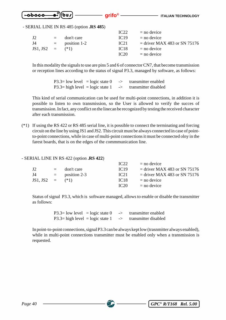
SERIAL COMMUNICATION SELECTION
GPC® R/T168 serial line can be buffered as RS 232, RS 422, RS 485 or Current Loop. By hardwarecan be selected which one of these electric standards is used, through jumpers connection and driversinstallation. By software the serial line can be programmed to operate with all the standard physicalprotocols, in fact the bits per character, parity, stop bits and baud rates can be decided by settingopportunes CPU internal registers. In the following paragraphs there are all the informations on serialcommunication configurations.Some devices needed for RS 422, RS 485 and Current Loop configurations are not mounted on theboard in standard configuration; this is why each fist non-standard (non-RS 232) serial configurationmust be always performed by grifo ® technicians. This far the User can change in autonomy theconfiguration following the informations below:
- SERIAL LINE A (hardware) IN RS 232 (default configuration)IC22 = driver MAX 202
J2 = don't care IC19 = no deviceJ4 = don't care IC21 = no deviceJS1, JS2 = not connected IC18 = no device
IC20 = no device
- SERIAL LINE B (software) ONLY RS 232 (default configuration)IC22 = driver MAX 202
J2 = 2-3 IC19 = no deviceJ4 = don't care IC21 = no deviceJS1, JS2 = not connected IC18 = no device
IC20 = no device
- SERIAL LINE IN CURRENT LOOP (option .CLOOP)IC22 = no device
J2 = don't care IC19 = no deviceJ4 = don't care IC21 = no deviceJS1, JS2 = not connected IC18 = driver HP 4100
IC20 = driver HP 4200
Please remark that Current Loop serial interface is passive, so it must be connected an activeCurrent Loop serial line, that is a line provided with its own power supply. Current Loopinterface can be employed to make both point-to-point and multi-point connections througha 2-wires or a 4-wires connection.
ITALIAN TECHNOLOGY grifo ®
Page 39 GPC® R/T168 Rel. 5.00
FIGURE 36: GPC® T168 JUMPERS LOCATION ON COMPONENT SIDE
FIGURE 37: GPC® T168 JUMPERS LOCATION ON SOLDER SIDE
J1
J5
J2
J4
J3
JS2 JS1
grifo ® ITALIAN TECHNOLOGY
Page 40 GPC® R/T168 Rel. 5.00
- SERIAL LINE IN RS 485 (option .RS 485)IC22 = no device
J2 = don't care IC19 = no deviceJ4 = position 1-2 IC21 = driver MAX 483 or SN 75176JS1, JS2 = (*1) IC18 = no device
IC20 = no device
In this modality the signals to use are pins 5 and 6 of connector CN7, that become transmissionor reception lines according to the status of signal P3.3, managed by software, as follows:
P3.3= low level = logic state 0 -> transmitter enabledP3.3= high level = logic state 1 -> transmitter disabled
This kind of serial communication can be used for multi-point connections, in addition it ispossible to listen to own transmission, so the User is allowed to verify the succes oftransmission. In fact, any conflict on the linecan be recognized by testing the received characterafter each transmission.
(*1) If using the RS 422 or RS 485 serial line, it is possible to connect the terminating and forcingcircuit on the line by using JS1 and JS2. This circuit must be always connected in case of point-to-point connections, while in case of multi-point connections it must be connected olny in thefarest boards, that is on the edges of the commmunication line.
- SERIAL LINE IN RS 422 (option .RS 422)IC22 = no device
J2 = don't care IC19 = driver MAX 483 or SN 75176J4 = position 2-3 IC21 = driver MAX 483 or SN 75176JS1, JS2 = (*1) IC18 = no device
IC20 = no device
Status of signal P3.3, which is software managed, allows to enable or disable the transmitteras follows:
P3.3= low level = logic state 0 -> transmitter enabledP3.3= high level = logic state 1 -> transmitter disabled
In point-to-point connections, signal P3.3 can be always kept low (trasnmitter always enabled),while in multi-point connections transmitter must be enabled only when a transmission isrequested.
ITALIAN TECHNOLOGY grifo ®
Page 41 GPC® R/T168 Rel. 5.00
Serial in RS 232 Serial in Current-Loop
Serial in RS 422 Serial in RS 485
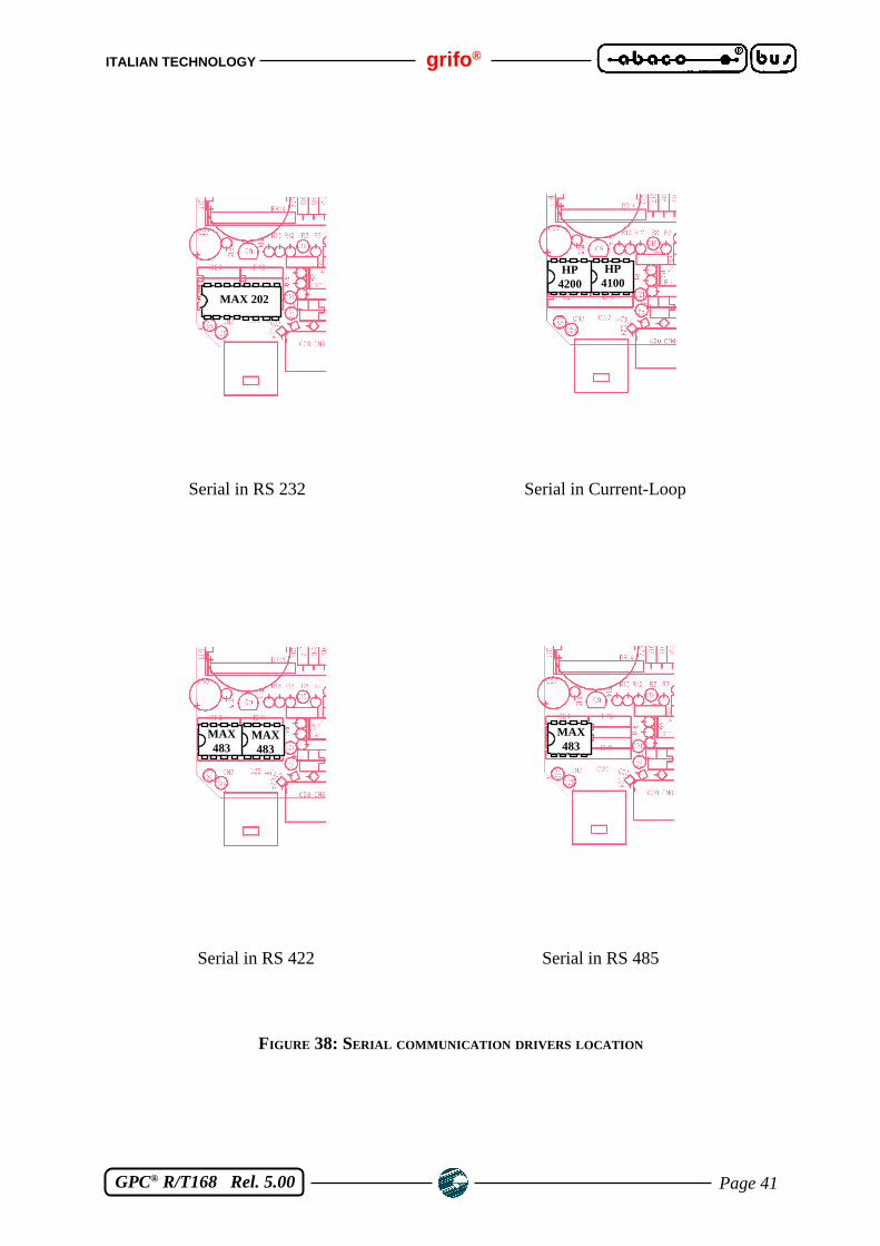
FIGURE 38: SERIAL COMMUNICATION DRIVERS LOCATION
HP4100
HP4200
MAX483
MAX483
MAX483
MAX 202

grifo ® ITALIAN TECHNOLOGY
Page 42 GPC® R/T168 Rel. 5.00
IN SYSTEM PROGRAMMING (ISP)
One of the most important features of GPC® R/T 168 is the possibility to employ the newmicroprocessors PHILIPS 89CRx2 that support in system programming, this means that the CPUFLASH can be programmed directly on the board, without any need to remove the CPU. Here followsthe steps to perform for ISP:
1) develop the application program usign a software tools capable to generate executable code2) connect jumpers J3 and J1 in position 1-23) connect serial line A in RS 232 to a personal computer COM port4) supply the board, program the microprocessor internal FLASH EPROM using the specific
software tool provided by PHILIPS: WINISP .5) remove power supply to the board6) connect J3 and J1 in position 2-3 to enable the microprocessor internal EPROM7) supply the board again: the application program is now executed from internal EPROM.
ISP reduces the total cost of the application, in fact it allows to do without EPROMs, EPROMprogrammer, FLASH EPROM, etc.For further information about ISP programming please refer to the specific technical documentationby PHILIPS.
RESET AND WATCH DOG
On GPC® R/T168 there is a watch dog circuit (not all the microprocessors are provided with it) thatis really efficient and easy to use. The most important features of such circuitery are:
- astable mode; - intervention time tipically programmable; - retrigger by software;
In astable mode when intervention time is elapsed the circuit becomes active, it stays active till theend of reset time and after it is again deactivated.Please remark that another reset source, in addition to the eventual watch dog circuit, is power oncircuitery.
ITALIAN TECHNOLOGY grifo ®
Page 43 GPC® R/T168 Rel. 5.00
SOFTWARESOFTWARE
A wide selection of software development tools can be obtained, allowing use of the GPC® R/T168card as a system for its own development, both in assembler and in other high level languages; inthis way the user can easily develop all the requested application programs in a very short time.Generally all software packages available for the51 microprocessors family can be used.
MICRO/ASM-51 : macro cross assembler available for MS-DOS operating system in "ABSOLUTE"and "RELOCATABLE" version. In this "RELOCATABLE" version is supplied with a linker anda library manager.
MICRO/C-51 : integer cross compiler for source files in standard ANSI C, available also for MS-DOS operating system. It produces a source assembly file compatible with MICRO/ASM-51 or withIntel macro relocatable assembler MCS 51.
MICRO/SLD-51 : source level debugger and simulator. It is executed on P.C. without any additionalhardware and it allows loading of HEX and SYMBOLIC files, breakpoint setting, instructionexecution in trace mode, registers and memory dump, etc.
HI-TECH C : cross compiler for C source program. It is a powerful software tool that includes editor,C compiler, assembler, optimizer, linker, library, and remote symbolic debugger, in one easy to useintegrated development environment.
BASCOM 8051: cross compiler for BASIC source program. It is a powerful software tool thatincludes editor, BASIC compiler and simulator included in an easy to use integrated developmentenvironment for Windows. Many memory models, data types and direct use of hardware resourceinstructions are available.
DDS MICRO C 51: low cost ross compiler for C source program. It is a powerful software tool thatincludes editor, C compiler (integer), assembler, optimizer, linker, library, and remote debugger, inone easy to use integrated development environment. There are also included the library sources andmany utilities programs.

grifo ® ITALIAN TECHNOLOGY
Page 44 GPC® R/T168 Rel. 5.00
ADDRESSINGADDRESSING
INTRODUCTION
In this chapter all the information related to the software programming of the board will be given.Such information include the software management of all the section.
ON BOARD RESOURCES ADDRESSING
The on board devices are addressed in two modes: the classic 16 bit parallel bus for FLASH EPROMand SRAM and the devices connected to the two-wires serial I 2C-BUS.These latter devices have the addresses reported in the following paragraph and cannot be reallocatedto any other address. The devices connected to I 2C-BUS are managed by the microcontroller throughtwo generic I/O lines, clock signal (SCL, P3.5 pin 17) and data signal (SDA, P3.4 pin 16).
P3.4 <-> DATA signal (SDA)P3.5 -> CLOCK signal (SCL)
I 2C-BUS PERIPHERALS MAPPING
All the devices interfacing through protocol I 2C-BUS have an unchangeable internal code (A6, A5,A4, A3), many of these devices may have from one to three pins associated to three address signals(A2, A1, A0), so it is possible to connect together several devices having the same internal code. Herewe report the device name, its purpose and slave address:
FIGURE 39: I2C-BUS PERIPHERALS ADRESSING TABLE
Letter "X" indicates that the component can be read and written, it must be indicated because thereare components that can be only read or only written, in these caseW/R will be 0 for writeable, 1 forreadable. The software description of the components indicated int the table is contained in thechapter “PERIPHERAL DEVICES SOFTWARE DESCRIPTION”.
DEVICE IC FUNCTIONI 2C-BUS SLAVE ADDRESS
Bit 7 6 5 4 3 2 1 0A6 A5 A4 A3 A2 A1 A0 W/R
PCF8575 IC15 16 I/O Expander 0 1 0 0 0 0 0 X
PCF8591 IC1 4 A/D, 1 D/A 1 0 0 1 0 0 0 X
PCF8583 IC8RTC +
256 bytes RAM1 0 1 0 0 0 0 X
24c04 or 24c08 IC9EEPROM
512÷1024bytes1 0 1 0 1 0 0 X

ITALIAN TECHNOLOGY grifo ®
Page 45 GPC® R/T168 Rel. 5.00
FIGURE 40: MEMORY ADDRESSING TABLE
8000H7FFFH
FEFFH
INTERNALCODE AREA
0000H
EXTERNALDATA AREA
7FFFH
32 K
0000H
IC10RAM
IC12CPU
7FFFH
32 K
0000H
FFFFH
3FFFH
1FFFH8 K
16 K
64 K
32 K

grifo ® ITALIAN TECHNOLOGY
Page 46 GPC® R/T168 Rel. 5.00
PERIPHERAL DEVICES SOFTWARE DESCRIPTIONPERIPHERAL DEVICES SOFTWARE DESCRIPTION
The previuos paragraph reported the allocation addresses of all the perpherals, in this chapter isreported the detailed description of purpose and meaning of their registers (to correctly understandthe following information please refer to the I 2C-BUS addressing table). Should the presentdocumentation be insufficent please refer to manufacturer documentation. For furhter informationabout programming the CPU sections please refer to the CPU manufacturer documentation.
BACKED SRAM + RTC
For further information about the PCF8583 serial module (IC8), please refer to the manifacturerdocumentation, because it contains several registers. This paragraph does not give detailed softwareinformation because the management of this device is complicated and requires a deep knowledgeof the device itself, anyway the user can take advantage of the specific high level procedurescontained in the examples. The component contains 256 registers, from 0 to 0FH the timer or clockregisters are present, remaining addresses from 10H to FFH correspond to backed memory locations,please refer also to jumper J5 description.
Slave Address reading writingPCF8583 A1H A0H
We would want to remark that if this device is not installed on IC8 the maximum eeprom size for IC4is 2048 byte (24c16), when IC8 is installed the maximmum eeprom size is 1024 byte (24c08). Towrite to a memory location use the followint sequence:Slave address writing+ register num. (0÷FFH) + data to writeTo read from a memory location use the followint sequence:Slave address writing+ register num. (0÷FFH)Slave address reading + data to read
SERIAL EEPROM
The management modalities of serial EEPROM installed on IC9 is the same of SRAM+RTC, onlythe slave addresses change as they are bound to eeprom size. Infact the eeprom that can be installedare: 24c01 (0÷7FH byte), 24c02 (0÷FFH byte), 24c04 (0÷1FFH byte), 24c08 (0÷3FFH byte), 24c16(0÷7FFH byte) this latter can be installed only if SRAM+RTC is not installed on IC8. Examining thesequence given for SRAM+RTC we can see that available registers range from 0 to FFH, so up tomodel 24c02there are no differences except for the slave address, please remark that if slave addressis even a writing operation is performed, if odd a reading operation is performed.
Slave Address reading writing register n° memory24c01 A9H A8H 0÷7FH 128 byte24c02 A9H A8H 0÷FFH 256 byteOf course 24c01 does not have valid registers in the range 80H÷FFH.8 bit are not enough to manage the biggest eeprom, to reach the address 1024 (24c08 1FFH) 10 bitare essential, so the first 8 bit will be set as register number, most significant 2 bit will be A0 and A1,please see figure 39.

ITALIAN TECHNOLOGY grifo ®
Page 47 GPC® R/T168 Rel. 5.00
Slave Address reading writing register n° memory24c04 A9H÷ABH A8H÷AAH 0÷FFH 512 byte24c08 A9H÷AEH A8H÷AFH 0÷FFH 1024 byteWhile with a 24c16 the slave address is:
Slave Address reading writing register n° memory24c16 A0H÷AEH A1H÷AFH 0÷FFH 2048 byte
Here it is evident that this eeprom is in conflict with SRAM+RTC, because they have the same slaveaddress (A0H).
4 A/D AND 1 D/A
The IC PCF8591 installed on IC1, allows to aquire 4 analog input channels and to drive one analogoutput with 8 bit of resolution, all the signals are in the range da 0÷2.5Vdc. Through I 2C-BUS writingto this peripheral the control register is accessed, the next byte in writing is the eventual value for theanalog output,while in reading the first byte returns the value of the conversion on the channelpreviously requested, the second byte indicates the value of the conversion on the channel requested.The first operation is to set the control register,to easily understand the bits of control register pleaserefer to figure 41.There it is shown that bit 7 and bit 3 have no meaning and must be kept at logic level zero, bit 6 if1 activates the analog input, bit 5 and 4 configure the 4 analog channels in 4 different modes:
- 4 channels single polarity- 3 differential channels on ch3- 2 channels single polarity and 1 differential channel- 2 differential channels.
Bit 2 if 1 allows to switch automatically to the next channel to convert, while bits 1 and 0 select thechannel convert, so only this latter two bits will be changed to acquire all the channels withoutfollowing an automatic sequence.
Slave Address reading writingPCF8591 91H 90H
In the following example the device will be configured with D/A enabled, 4 channells single polarity:point to channell 0, control register 40H.Writing: 90H, 40H, data for D/AReading: 91H, data previous A/D channel, data channel 0 chosen by control register

grifo ® ITALIAN TECHNOLOGY
Page 48 GPC® R/T168 Rel. 5.00
Bit 7 6 5 4 3 2 1 0
FIGURE 41: A/D AND D/A CONTROL REGISTERS
For further information please refer to manufacturer documentation.
I/O EXPANDER
This peripheral is managed through I 2C-BUS, the component is installed in IC15, this allows to driveeight digital TTL signals in input or in output. Management is easy, when a read operation isperformed (Slave Address W/R=1 + data) they are set as input, while to perfrorm a write operation(Slave Address W/R=0 + data) they are set as output, to set the lines back to input first they must beconnected to a logic level high then a read operation will set then ad input, please remark that afterthe power on all lines are set as input. A remarkable feature of this component is the ability to triggeran interrupt whenever a inputs change logic level (see jumper J2), thanks to this feature it is notessential to read continuously inputs, it is enough to manage the interrupts and to acquire the lines.
ITALIAN TECHNOLOGY grifo ®
Page 49 GPC® R/T168 Rel. 5.00
Slave Address reading writing
PCF8575 41H 40H
For furhter information please refer to the manifacturer documentation.PORT 0 is used as input to read the 8 optocoupled inputs on CN5, while PORT 1 is used as outputfor relays or transistor outputs on CN4.
DIGITAL INPUTS
Acquisition of optocoupled inputs (CN2) is performed through 8 microcontroller lines (PORT 1),while the remaining 8 lines (CN5) are managed through PORT 0 of IC15 (PCF8575).To acquire CN2, the microcontroller must read its PORT 1, while to acquire CN5 an I 2C-BUSsequence must be started to read PORT 0 of IC15, as in the following example:
Slave address read + data to readRead: 41H, PORT0
Please remark that this latter device generater an interrupt whenever a logic input changes its status(see jumper J2). When an NPN input is actived (contact closed to GND opto), the corresponding lineis at logic level low (logic 0), viceversa an input is disactived (contact open) puts the correspondingline to logic level low (logic 1).
DIGITAL OUTPUTS
The eight NPN relays or transistor outputs are set through PORT1 of IC15 (PCF8575), managed inI 2C-BUS, as in the following exampl:
Slave address write + data to writewrite: 40H, PORT0, PORT1
To avoid confilcts between optocouplers input circuit and PORT 0, this latter must be always set toFFH (255), this prevents problems that may verify when PORT 0 is used as input. In this case theuser can take advantage of the specific high level language procedures provided in the examples.When an I/O line is set to logic state low (logic 0), the corresponding output is actived (transitorconducing or relay contact connected to is common), viceversa when a line is set to logic state high(logic 1) the corresponding output is disactived (transistor not conducing or relay contact open).When a power on occours, I/O lines are set to logic 1, so the relays or transistors are disactived.
CPU PERIPHERALS
For further information about CPU internal peripherals registers and their purpose (Timer Counter,interrupts controller, serial line, I/O ports , etc) please refer to manufacturer documentation.

grifo ® ITALIAN TECHNOLOGY
Page 50 GPC® R/T168 Rel. 5.00
BIBLIOGRAPHYBIBLIOGRAPHY
Here follows a list of manuals and technical notes that the User can read to acquire more informationsabout GPC® R/T168 board.
Manual TEXAS INSTRUMENTS: The TTL Data Book - SN54/74 FamiliesManual TEXAS INSTRUMENTS: RS-422 and RS-485 Interface Circuits
Manual MAXIM: New Releases Data Book - Volume 4
Manual XICOR: Data Book
Manual PHILIPS: IC1, IC8,IC9, IC15 - I2C bus
Manual ATMEL: Microcontroller - AT89 series
Manual PHILIPS: 80C51 - Based 8-Bit Microcontrollers
Manual TOSHIBA: Photo Couplers - Data Book
Manual MOTOROLA: Bipolar Power Transistor Data
Technical notes: LM2825N
Please connect to the manifactures Web sites to get the latest version of all manuals and data sheets.

ITALIAN TECHNOLOGY grifo ®
Page 51 GPC® R/T168 Rel. 5.00
1 H
ardw
are
Ser
ial
Line
RS
-232
, RS
42
2, R
S 4
85 o
r C
urre
nt L
oop
8 O
UT
PU
T L
INE
S
RE
LAY
S o
r T
RA
NS
IST
OR
S
DIN
462
77-1
and
DIN
462
77-3
OM
EG
A R
AIL
S
P L
C
QT
P te
rmin
als
GP
C®
R/T
94P
C li
ke o
rM
acin
tosh
8 B
its4
Ana
log
inpu
ts:
0÷2,
5 V
dc VA
8 B
its1
Ana
log
outp
ut:
0÷2,
5 V
dc
GP
C®
R/T
63
DA
C
ON
BO
AR
D R
EA
L T
IME
CLO
CK
,LI
TH
IUM
BA
TT
ER
Y fo
rB
ack
Up
+ -
8+8
INP
UT
LIN
ES
OP
TO
CO
UP
LED
+10
÷40
Vdc
or+
8÷24
Vac
+V
opto
(+24
Vdc
)P
OW
ER
SU
PP
LY
FIGURE 42: POSSIBLE CONNECTIONS DIAGRAM

grifo ® ITALIAN TECHNOLOGY
Page 52 GPC® R/T168 Rel. 5.00
ITALIAN TECHNOLOGY grifo ®
Page A-1 GPC® R/T168 Rel. 5.00
APPENDIX A: ALPHABETICAL INDEXAPPENDIX A: ALPHABETICAL INDEX
SYMBOLS
+VL 27µP AT89C5 4µP AT89C52 4µP AT89S8252 4
A
A/D 47A/D AND D/A CONVERTER 7A/D CONVERTER 30, 32A/D CONVERTER ELECTRIC FEATURES 10A/D CONVERTER GENERAL FEATURES 8ADDRESSING 44ASTABLE MODE 42
B
BACK UP 32BACK UP CURRENT 10BIBLIOGRAPHY 50BT1 32
C
CARD VERSION 1CLOCK DEVICES 6CONNECTIONS 14CONNECTORS 8, 11
CN1 30CN2 22CN4 26CN5 23CN6 14CN7 16CN8 27
CPU 4, 8CPU CLOCK FREQUENCE 8CPU PERIPHERALS 49CURRENT CONSUMPTION 10, 12CURRENT LOOP 7, 16, 32, 38

grifo ® ITALIAN TECHNOLOGY
Page A-2 GPC® R/T168 Rel. 5.00
D
D/A 47D/A CONVERTER 30D/A CONVERTER ELECTRIC FEATURES 10D/A CONVERTER GENERAL FEATURES 8DIGITAL INPUTS 49DIGITAL OUTPUTS 49
G
GENERAL FEATURES 2GPC® R168 ELECTRIC FEATURES 10GPC® R168 GENERAL FEATURES 8GPC® R168 PHYSICAL FEATURES 8GPC® R168 TECHNICAL FEATURES 8GPC® T168 ELECTRIC FEATURES 12GPC® T168 GENERAL FEATURES 11GPC® T168 PHYSICAL FEATURES 11GPC® T168 TECHNICAL FEATURES 11
I
I/O CONNECTION 32I/O EXPANDER 48I 2C BUS 44IN SYSTEM PROGRAMMING 42INPUT SECTION 7INPUT SIGNALS 23INSTALLATION 14INTERRUPTS 32INTRODUCTION 1ISP 42
J
JUMPERS 352 PINS JUMPERS 353 PINS JUMPERS 36
L
LITHIUM BATTERY 32
M
MEMORY 8MEMORY DEVICES 6MEMORY SELECTION 37MOUNTING 8, 11

ITALIAN TECHNOLOGY grifo ®
Page A-3 GPC® R/T168 Rel. 5.00
N
NPN INPUTS MINIMUM CURRENT 10
O
ON BOARD BACK UP BATTERY 10ON BOARD RESOURCES 8, 11ON BOARD RESOURCES ADDRESSING44
P
PBI 01 24PERIPHERAL DEVICES SOFTWARE DESCRIPTION46PERIPHERALS MAPPING 44PNP DRIVERS 24POWER SUPPLY 4, 10, 14, 16, 34
R
REAL TIME CLOCK 6RELATIVE HUMIDITY 10RELAYS MAXIMUM CURRENT 10RELAYS OUTPUTS 6, 26RESET 42RS 232 7, 16, 32, 38RS 422 7, 16, 32, 40RS 485 7, 16, 32, 40RS422-485 TERMINATION NETWORK 10RTC 32, 37, 46RTC CLOCK FREQUENCE 8
S
SERIAL COMMUNICATION SELECTION 7, 38SERIAL EEPROM 6, 37, 46SIZE 8, 11SOFTWARE 43SOLDER JUMPERS 34SRAM 6, 8, 32, 37, 46SWITCHING 4
grifo ® ITALIAN TECHNOLOGY
Page A-4 GPC® R/T168 Rel. 5.00
T
TEMPERATURE RANGE 10TRANSISTOR OUTPUTS 6, 27TRANSISTORS MAXIMUM CURRENT 12TRANSISTORS MAXIMUM POWER 12TRANSISTORS MAXIMUM VOLTAGE 12TRANSZORB™ 4, 34
W
WATCH DOG 42WEIGHT 8, 11WINISP 42