Embed Size (px)
Citation preview
Copyright © 2016 Next Thing Co. All Rights Reserved.
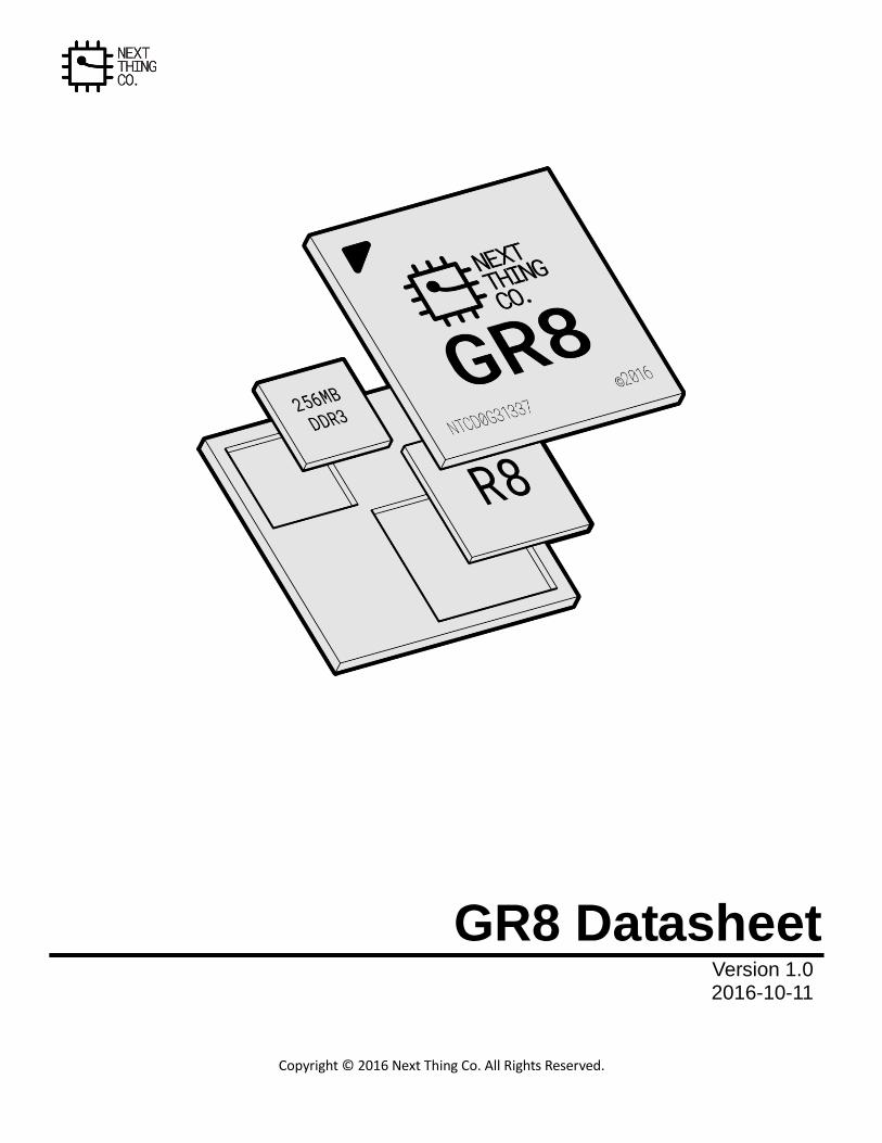
GR8 Datasheet Version 1.0 2016-10-11
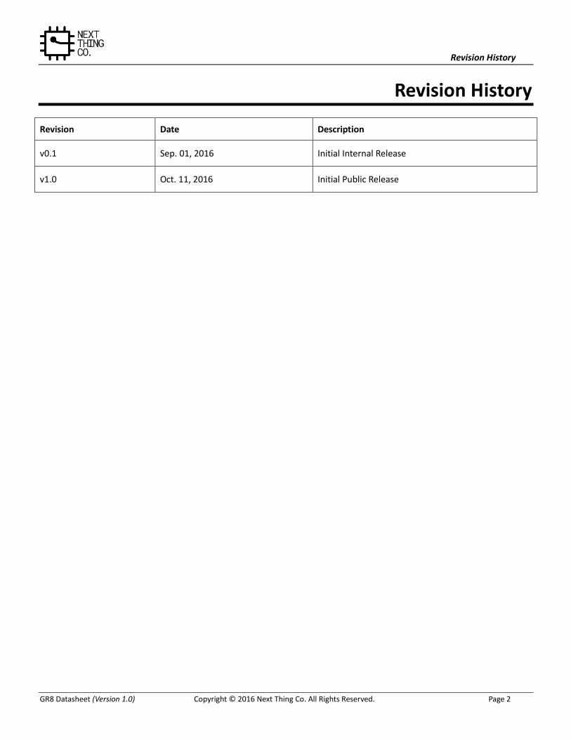
Revision History
GR8 Datasheet (Version 1.0) Copyright © 2016 Next Thing Co. All Rights Reserved. Page 2
Revision History
Revision Date Description
v0.1 Sep. 01, 2016 Initial Internal Release
v1.0 Oct. 11, 2016 Initial Public Release
Declaration
Copyright © 2016 Next Thing Co. All Rights Reserved.
Declaration
This page left intentionally blank. \(•◡•)/ .
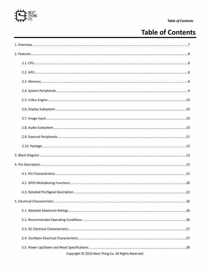
Table of Contents
Copyright © 2016 Next Thing Co. All Rights Reserved.
Table of Contents 1. Overview ........................................................................................................................................................................... 7
2. Features ............................................................................................................................................................................. 8
2.1. CPU ......................................................................................................................................................................... 8
2.2. GPU ........................................................................................................................................................................ 8
2.3. Memory .................................................................................................................................................................. 8
2.4. System Peripherals ................................................................................................................................................. 9
2.5. Video Engine ........................................................................................................................................................ 10
2.6. Display Subsystem ................................................................................................................................................ 10
2.7. Image Input .......................................................................................................................................................... 10
2.8. Audio Subsystem .................................................................................................................................................. 10
2.9. External Peripherals ............................................................................................................................................. 11
2.10. Package .............................................................................................................................................................. 12
3. Block Diagram ................................................................................................................................................................. 13
4. Pin Description ................................................................................................................................................................ 15
4.1. Pin Characteristics ................................................................................................................................................ 15
4.2. GPIO Multiplexing Functions ................................................................................................................................ 20
4.3. Detailed Pin/Signal Description ............................................................................................................................ 22
5. Electrical Characteristics ................................................................................................................................................. 26
5.1. Absolute Maximum Ratings ................................................................................................................................. 26
5.2. Recommended Operating Conditions .................................................................................................................. 26
5.3. DC Electrical Characteristics ................................................................................................................................. 27
5.4. Oscillator Electrical Characteristics ...................................................................................................................... 27
5.5. Power Up/Down and Reset Specifications ........................................................................................................... 28
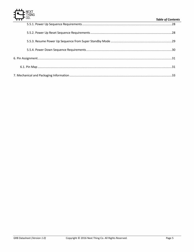
Table of Contents
GR8 Datasheet (Version 1.0) Copyright © 2016 Next Thing Co. All Rights Reserved. Page 5
5.5.1. Power Up Sequence Requirements ........................................................................................................... 28
5.5.2. Power Up Reset Sequence Requirements ................................................................................................. 28
5.5.3. Resume Power Up Sequence from Super Standby Mode ......................................................................... 29
5.5.4. Power Down Sequence Requirements ...................................................................................................... 30
6. Pin Assignment ................................................................................................................................................................ 31
6.1. Pin Map ................................................................................................................................................................ 31
7. Mechanical and Packaging Information .......................................................................................................................... 33

About This Documentation
GR8 Datasheet (Version 1.0) Copyright © 2016 Next Thing Co. All Rights Reserved. Page 6
About This Documentation
From the desk of Gustavo Huber
When Dave, Thomas, and I started Next Thing Co. in 2013, it was with a simple goal: we wanted to create things that would inspire creativity, and help people chase their own ideas of what needed to exist. We considered this goal both in terms of how economically accessible we could make our products (they had to be $99 or less), as well as how much “pain” we could remove from the design process for others (they had to be open source and well-documented). Our first attempt was a software-defined camera named OTTO, built around an off-the-shelf embedded module. But early in development, we knew that our end-goals were at risk. The $39 module made it impossible to ship product priced under $99. It lacked Mainline Linux support, a reliable tool-chain, documentation and functional drivers making software development a cat-and-mouse game of bug tracking. But thanks to lots of long days, and some good friends both in Shenzhen and back home in Oakland, we built and shipped out 500 OTTOs -- a serious feat. Almost exactly a year later, we shipped out the first of what is now over 100,000 C.H.I.P.s delivered worldwide. At $9, C.H.I.P. was the fruition of our vision from a year prior: accessible, powerful technology, available to everyone for hobby, education, or products. In so many words, we were building the tools that we wished we’d had before. The reaction was (and continues to be) astounding! Tweets and emails come from far and wide to tell us about impossible projects banged together in an afternoon, classrooms full of proud 10-year-old game developers who had never before written a line of code, and seasoned engineers brought back to memories of discovering their passion on a Commodore 64, 40 years prior. Yet, just as building OTTO showed us the tools we were missing, building C.H.I.P has taught us what it takes to scale production to keep up with [even unprecedented] demand. So it is with great pleasure that I invite you to explore, without non-disclosure agreements or any other obstructive formalities, this datasheet for GR8: the newest addition to the Next Thing Co. family. Thanks to the experience and support from our friends at Allwinner and Nanya, GR8 is built from the ground up for clean and reliable design. With Next Thing Co. and the thriving Chipster community from bbs.nextthing.co at your side, we can’t wait to see what you’ll do with GR8! /Gustavo Co-founder, Hardware Guy
Overview
GR8 Datasheet (Version 1.0) Copyright © 2016 Next Thing Co. All Rights Reserved. Page 7
1. Overview
At Next Thing Co., we work to make it easy to integrate computer hardware in products. GR8 provides a powerful application processor and DDR3 SRAM which eliminates the need for high-speed routing and reduces manufacturing complexity. GR8 is a System-in-Package (SiP) that features a 1GHz Allwinner R8 ARMv7 Cortex-A8 processor with NEON SIMD extensions and a Mali-400 GPU. 256MB of Nanya DDR3 SDRAM is combined with the R8 processor into a 14mm x 14mm, 0.8mm pitch 252 ball FBGA package.
In addition to the Mali-400 graphic engine that supports OpenGL ES 1.0 and 2.0. GR8 includes a video engine for encoding and decoding codecs such as VP6/8, AVS, H.264, H.263, MPEG-1/2/4 and a display engine for a hardware cursor, alpha blending, and anti-flicker.
GR8 also features many popular peripheral interfaces: Two-Wire Interface, two UARTs (one 2-wire and one 4-wire), SD Card-ready SPI, two PWM outputs, a 6-bit ADC, I2S digital audio, S/PDIF IEC-60958 digital audio output, two HS/FS/LS USB PHYs (one USB 2.0 Host and one USB 2.0 OTG), a CMOS Sensor Interface. GR8 is $6 in any quantity and includes the Allwinner AXP209 power management unit. The minimum order quantity for GR8 + AXP209 is one.
We can’t wait to see how you’ll design GR8 in to your next product.
1.1. Applications
Physical Computing
Voice Recognition
Smart “Clapper”
Animated GIF Camera
Smart Consumer Devices
Portable Audio Devices
Cyber Dog Robot Toys
Features
GR8 Datasheet (Version 1.0) Copyright © 2016 Next Thing Co. All Rights Reserved. Page 8
2. Features
2.1. CPU
• ARM CortexTM-A8 • ARMv7 Instruction set plus Thumb-2 Instruction Set • 32KB Instruction Cache and 32KB Data Cache • 256KB L2 Cache • NEONTM SIMD Extensions • Jazelle RCT Acceleration
2.2. GPU
• Mali400 • Supports Open GL ES 1.1/ 2.0 and Open VG 1.1
2.3. Memory
Boot ROM • On-chip Boot ROM • Supports boot from NAND Flash, SPI NOR Flash, SD Card and USB OTG
NANYA DDR3 SDRAM • In-package 256MB 16-bit DDR3 memory
NAND Flash • Compliant with ONFI 2.3 and Toggle 1.0 • Up to 8-bit data bus width • Supports 2 chip selects, and 2 ready/busy signals • Up to 64-bit ECC per 512 bytes or 1024 bytes • Supports 1KB/2KB/4KB/8KB/16KB page size • Supports SLC/MLC NAND and EF-NAND • Supports SDR/Toggle DDR/ONFI DDR NAND interface
SD/MMC • Three SD/MMC Host Controllers (SMHC) • Compatible with eMMC v4.4, SD Physical Layer Specification v2.0, SDIO Card Specification v2.0 • 1-/4-/8-bit bus width • Supports block size of 1 to 65535 bytes • Dedicated DMA for fast and uninterrupted data transfer
Features
GR8 Datasheet (Version 1.0) Copyright © 2016 Next Thing Co. All Rights Reserved. Page 9
2.4. System Peripherals
CCM – Clock Control Module • Seven PLLs driven by a main external Oscillator and an on-chip RC Oscillator • Supports clock configuration and clock generated for corresponding modules • Supports software-controlled clock gating and software-controlled reset for corresponding modules
DMA – Direct Memory Access • Eight channels Normal DMA (NDMA) and eight channels Dedicated DMA (DDMA) • Supports memory-to-memory, memory-to-peripheral, peripheral-to-memory data transfer types • Transfer data width of 8/16/32-bit • Programmable DMA burst size
PWM – Pulse Width Modulation • Two outputs • Supports continuous and pulse waveforms • 0 - 100% adjustable duty cycle • Up to 24 MHz output frequency
Asynchronous Timer Unit • Six Asynchronous Timers with interrupt-based operation • A watchdog timer to generate reset signal or interrupt • Two 33-bit Audio/Video Sync(AVS) Counter to synchronize video and audio • One 64-bit Counter
Synchronous Timer Unit • Two Synchronic Timers with interrupt-based operation
Interrupt Controller • Normal interrupt requests (nIRQ) and fast interrupt requests (FIQ) • Supports 96 interrupt sources • 4-Level priority controller • External interrupt can be triggered according to edge or level-sensitivity LRADC– Low Resolution Analog-to-Digital Converter • Analog to digital converter with 6-bit resolution for key application • Supports multiple button press detection • Supports single, normal and continuous work mode • Sampling frequency up to 250 Hz
Crypto Engine • Supports AES, DES, 3DES, SHA-1, MD5 • Supports ECB, CBC modes for AES/DES/3DES
Features
GR8 Datasheet (Version 1.0) Copyright © 2016 Next Thing Co. All Rights Reserved. Page 10
• 128 bits, 192 bits and 256 bits key size for AES • 160-bit hardware Pseudo Random Number Generator (PRNG) with a 175 bit seed
2.5. Video Engine
Video Decoding • Supports multi-format video decoding of VP6/8, AVS, H.264, H.263, and MPEG-1/2/4 • Up to 1080p@30fps resolution
Video Encoding • Supports encoding in H.264 MP format • Up to 720p@30fps resolution
2.6. Display Subsystem
Display Processing • Four moveable and size-adjustable layers • Multi-format image input • Image enhancement processor • Alpha blending /anti-flicker • Hardware cursor • Output color correction (luminance/hue/saturation)
Display Output • LCD interface (CPU / Sync RGB) • Supports CVBS output (TV Out)
2.7. Image Input
• Supports 8-bit CMOS sensor interface • Supports BT656 interface • Maximum still capture resolution on parallel interface up to 5M • Maximum video capture resolution on parallel interface up to 1080p@30fps • Pixel clock up to 150MHz
2.8. Audio Subsystem
Audio Codec - Audio Compression / Decompression Module • On-chip 24-bit DAC for playback and ADC for recording • Supports analog/digital volume control • Supports 44.1 kHz, 48 kHz, 96 kHz, and 192 kHz sample rates • Stereo microphone input • Stereo headphone amplifier
Features
GR8 Datasheet (Version 1.0) Copyright © 2016 Next Thing Co. All Rights Reserved. Page 11
I2S/PCM – Inter-IC Sound / Pulse Code Modulation
• Selectable I2S or PCM on shared pins • Full-duplex synchronous serial interface • Configurable as a master or a slave • Audio data resolutions of 16, 20, 24 • I2S Audio data sample rate from 8 kHz to 192 kHz • Left Justified or Right Justified I2S • PCM supports 8-bit or 16-bit linear, 8-bit u-law, or 8-bit A-law companding sample format
• One 128x24-bits FIFO for data transmit and one 64x24-bits FIFO for data receive • Programmable FIFO thresholds
OWA - One Wire Audio • IEC-60958 transmitter functionality • Channel status insertion • Hardware parity generation • One 32×24bits FIFO (TX) for audio data transfer • Programmable FIFO thresholds
2.9. External Peripherals
USB – Universal Serial Bus ● One USB 2.0 OTG controller Complies with USB 2.0 Specification Supports High-Speed (HS,480 Mbit/s), Full-Speed (FS,12 Mbit/s) and Low-Speed (LS,1.5 Mbit/s) in host mode Supports High-Speed (HS, 480 Mbit/s), Full-Speed (FS, 12 Mbit/s) in device mode Up to 10 user-configurable endpoints in device mode
● One USB Host controller Complies with Enhanced Host Controller Interface(EHCI)Specification, Version 1.0, and the Open Host Controller
Interface(OHCI) Specification, Version 1.0a Supports High-Speed (HS, 480 Mbit/s), Full-Speed (FS, 12 Mbit/s), and Low-Speed (LS, 1.5 Mbit/s) mode
TWI - Two Wire Interface • Three TWI (Two-Wire Interface) controllers • Supports Standard mode (up to 100 kbit/s) and Fast mode (up to 400 kbit/s) • Configurable as a master or a slave • Capable of 10-bit addressing transactions UART - Universal Asynchronous Receiver/Transmitter • Four UART controllers
- UART0 with 2 wires - UART1 with 4 wires - UART2 with 4 wires - UART3 with 4 wires
• Compatible with industry-standard 16550 UARTs • Support for word length from 5 to 8 bits, an optional parity bit, and 1,1.5 or 2 stop bits • Programmable parity (even, odd and no parity)
Features
GR8 Datasheet (Version 1.0) Copyright © 2016 Next Thing Co. All Rights Reserved. Page 12
SPI
• Two SPI controllers that each have one Chip Select signal • Full-duplex synchronous serial interface • Configurable as a master or a slave • Polarity, phase and clock frequency are configurable
Consumer IR • One flexible receiver for consumer IR remote control • Programmable FIFO thresholds
2.10. Package
• FBGA 252 Ball SiP, 14 mm x 14 mm, 0.8 mm pitch
Block Diagram
GR8 Datasheet (Version1.0) Copyright © 2016 Next Thing Co. All Rights Reserved. Page 13
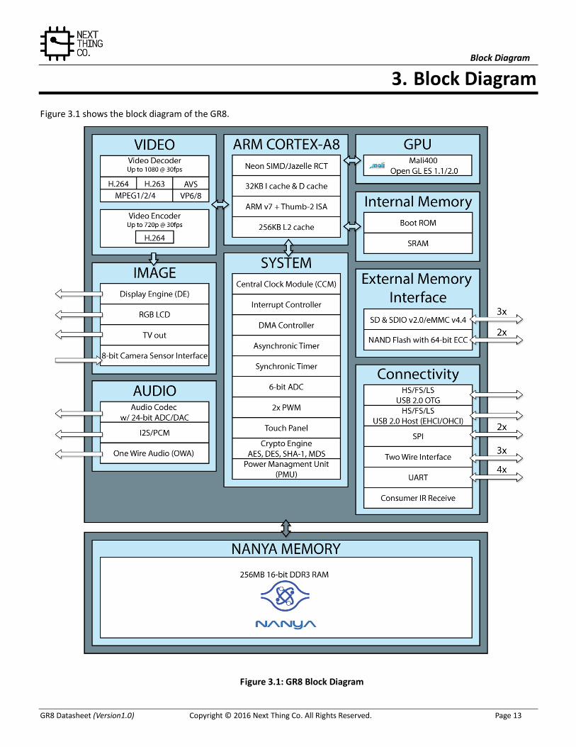
3. Block Diagram
Figure 3.1 shows the block diagram of the GR8.
Figure 3.1: GR8 Block Diagram
Block Diagram
GR8 Datasheet (Version1.0) Copyright © 2016 Next Thing Co. All Rights Reserved. Page 14
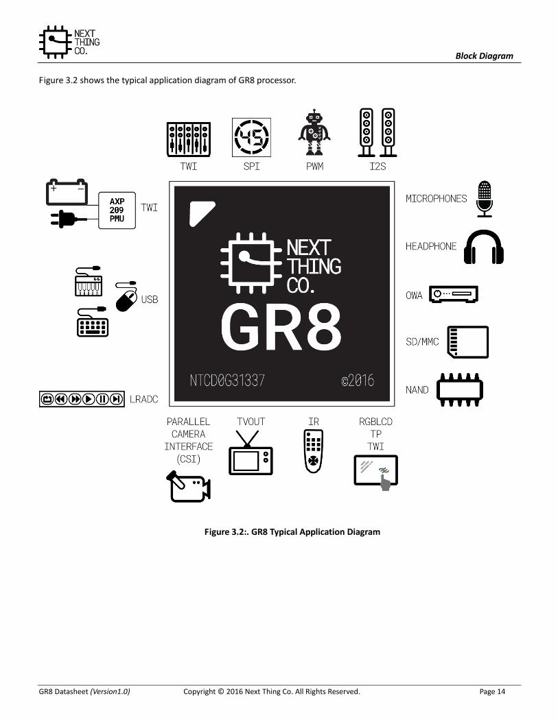
Figure 3.2 shows the typical application diagram of GR8 processor.
Figure 3.2:. GR8 Typical Application Diagram
Pin Description
GR8 Datasheet (Version1.0) Copyright © 2016 Next Thing Co. All Rights Reserved. Page 15
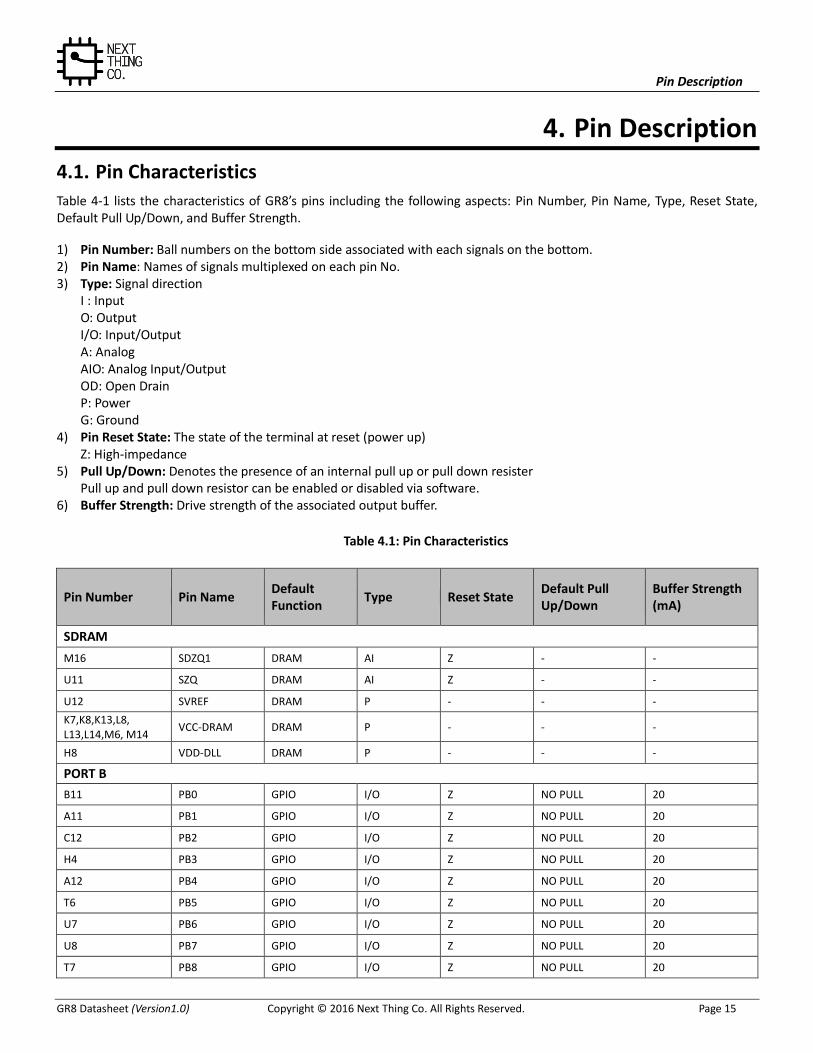
4. Pin Description
4.1. Pin Characteristics
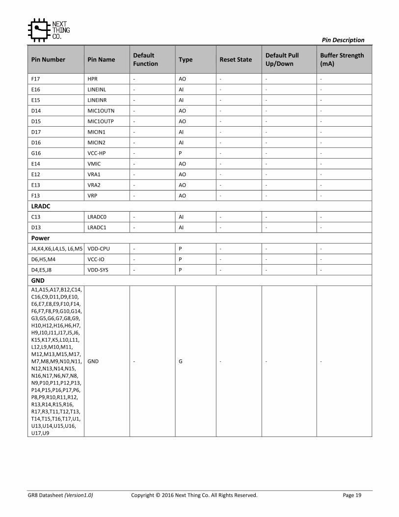
Table 4-1 lists the characteristics of GR8’s pins including the following aspects: Pin Number, Pin Name, Type, Reset State, Default Pull Up/Down, and Buffer Strength.
1) Pin Number: Ball numbers on the bottom side associated with each signals on the bottom. 2) Pin Name: Names of signals multiplexed on each pin No. 3) Type: Signal direction
I : Input O: Output I/O: Input/Output A: Analog AIO: Analog Input/Output OD: Open Drain P: Power G: Ground
4) Pin Reset State: The state of the terminal at reset (power up) Z: High-impedance
5) Pull Up/Down: Denotes the presence of an internal pull up or pull down resister Pull up and pull down resistor can be enabled or disabled via software.
6) Buffer Strength: Drive strength of the associated output buffer.
Table 4.1: Pin Characteristics
Pin Number Pin Name Default Function
Type Reset State Default Pull Up/Down
Buffer Strength (mA)
SDRAM
M16 SDZQ1 DRAM AI Z - -
U11 SZQ DRAM AI Z - -
U12 SVREF DRAM P - - -
K7,K8,K13,L8, L13,L14,M6, M14
VCC-DRAM DRAM P - - -
H8 VDD-DLL DRAM P - - -
PORT B
B11 PB0 GPIO I/O Z NO PULL 20
A11 PB1 GPIO I/O Z NO PULL 20
C12 PB2 GPIO I/O Z NO PULL 20
H4 PB3 GPIO I/O Z NO PULL 20
A12 PB4 GPIO I/O Z NO PULL 20
T6 PB5 GPIO I/O Z NO PULL 20
U7 PB6 GPIO I/O Z NO PULL 20
U8 PB7 GPIO I/O Z NO PULL 20
T7 PB8 GPIO I/O Z NO PULL 20
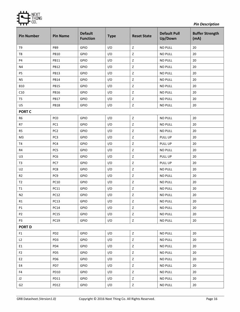
Pin Description
GR8 Datasheet (Version1.0) Copyright © 2016 Next Thing Co. All Rights Reserved. Page 16
Pin Number Pin Name Default Function
Type Reset State Default Pull Up/Down
Buffer Strength (mA)
T9 PB9 GPIO I/O Z NO PULL 20
T8 PB10 GPIO I/O Z NO PULL 20
P4 PB11 GPIO I/O Z NO PULL 20
N4 PB12 GPIO I/O Z NO PULL 20
P5 PB13 GPIO I/O Z NO PULL 20
N5 PB14 GPIO I/O Z NO PULL 20
B10 PB15 GPIO I/O Z NO PULL 20
C10 PB16 GPIO I/O Z NO PULL 20
T5 PB17 GPIO I/O Z NO PULL 20
U5 PB18 GPIO I/O Z NO PULL 20
PORT C
R6 PC0 GPIO I/O Z NO PULL 20
R7 PC1 GPIO I/O Z NO PULL 20
R5 PC2 GPIO I/O Z NO PULL 20
M3 PC3 GPIO I/O Z PULL UP 20
T4 PC4 GPIO I/O Z PULL UP 20
R4 PC5 GPIO I/O Z NO PULL 20
U3 PC6 GPIO I/O Z PULL UP 20
T3 PC7 GPIO I/O Z PULL UP 20
U2 PC8 GPIO I/O Z NO PULL 20
R2 PC9 GPIO I/O Z NO PULL 20
T2 PC10 GPIO I/O Z NO PULL 20
T1 PC11 GPIO I/O Z NO PULL 20
N2 PC12 GPIO I/O Z NO PULL 20
R1 PC13 GPIO I/O Z NO PULL 20
P1 PC14 GPIO I/O Z NO PULL 20
P2 PC15 GPIO I/O Z NO PULL 20
P3 PC19 GPIO I/O Z NO PULL 20
PORT D
F1 PD2 GPIO I/O Z NO PULL 20
L2 PD3 GPIO I/O Z NO PULL 20
E1 PD4 GPIO I/O Z NO PULL 20
F2 PD5 GPIO I/O Z NO PULL 20
E2 PD6 GPIO I/O Z NO PULL 20
E4 PD7 GPIO I/O Z NO PULL 20
F4 PD10 GPIO I/O Z NO PULL 20
J2 PD11 GPIO I/O Z NO PULL 20
G2 PD12 GPIO I/O Z NO PULL 20
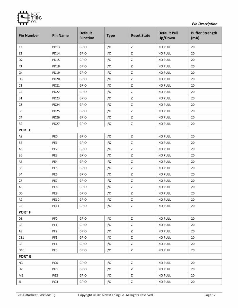
Pin Description
GR8 Datasheet (Version1.0) Copyright © 2016 Next Thing Co. All Rights Reserved. Page 17
Pin Number Pin Name Default Function
Type Reset State Default Pull Up/Down
Buffer Strength (mA)
K2 PD13 GPIO I/O Z NO PULL 20
E3 PD14 GPIO I/O Z NO PULL 20
D2 PD15 GPIO I/O Z NO PULL 20
F3 PD18 GPIO I/O Z NO PULL 20
G4 PD19 GPIO I/O Z NO PULL 20
D3 PD20 GPIO I/O Z NO PULL 20
C1 PD21 GPIO I/O Z NO PULL 20
C2 PD22 GPIO I/O Z NO PULL 20
B1 PD23 GPIO I/O Z NO PULL 20
C3 PD24 GPIO I/O Z NO PULL 20
B3 PD25 GPIO I/O Z NO PULL 20
C4 PD26 GPIO I/O Z NO PULL 20
B2 PD27 GPIO I/O Z NO PULL 20
PORT E
A8 PE0 GPIO I/O Z NO PULL 20
B7 PE1 GPIO I/O Z NO PULL 20
A6 PE2 GPIO I/O Z NO PULL 20
B5 PE3 GPIO I/O Z NO PULL 20
A5 PE4 GPIO I/O Z NO PULL 20
B6 PE5 GPIO I/O Z NO PULL 20
B4 PE6 GPIO I/O Z NO PULL 20
C7 PE7 GPIO I/O Z NO PULL 20
A3 PE8 GPIO I/O Z NO PULL 20
D5 PE9 GPIO I/O Z NO PULL 20
A2 PE10 GPIO I/O Z NO PULL 20
C5 PE11 GPIO I/O Z NO PULL 20
PORT F
D8 PF0 GPIO I/O Z NO PULL 20
B8 PF1 GPIO I/O Z NO PULL 20
A9 PF2 GPIO I/O Z NO PULL 20
C11 PF3 GPIO I/O Z NO PULL 20
B8 PF4 GPIO I/O Z NO PULL 20
D10 PF5 GPIO I/O Z NO PULL 20
PORT G
N3 PG0 GPIO I/O Z NO PULL 20
H2 PG1 GPIO I/O Z NO PULL 20
M1 PG2 GPIO I/O Z NO PULL 20
J1 PG3 GPIO I/O Z NO PULL 20
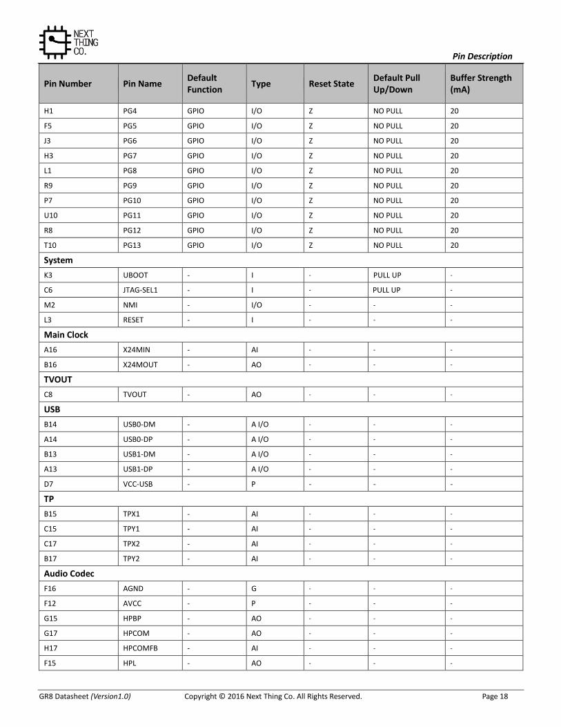
Pin Description
GR8 Datasheet (Version1.0) Copyright © 2016 Next Thing Co. All Rights Reserved. Page 18
Pin Number Pin Name Default Function
Type Reset State Default Pull Up/Down
Buffer Strength (mA)
H1 PG4 GPIO I/O Z NO PULL 20
F5 PG5 GPIO I/O Z NO PULL 20
J3 PG6 GPIO I/O Z NO PULL 20
H3 PG7 GPIO I/O Z NO PULL 20
L1 PG8 GPIO I/O Z NO PULL 20
R9 PG9 GPIO I/O Z NO PULL 20
P7 PG10 GPIO I/O Z NO PULL 20
U10 PG11 GPIO I/O Z NO PULL 20
R8 PG12 GPIO I/O Z NO PULL 20
T10 PG13 GPIO I/O Z NO PULL 20
System
K3 UBOOT - I - PULL UP -
C6 JTAG-SEL1 - I - PULL UP -
M2 NMI - I/O - - -
L3 RESET - I - - -
Main Clock
A16 X24MIN - AI - - -
B16 X24MOUT - AO - - -
TVOUT
C8 TVOUT - AO - - -
USB
B14 USB0-DM - A I/O - - -
A14 USB0-DP - A I/O - - -
B13 USB1-DM - A I/O - - -
A13 USB1-DP - A I/O - - -
D7 VCC-USB - P - - -
TP
B15 TPX1 - AI - - -
C15 TPY1 - AI - - -
C17 TPX2 - AI - - -
B17 TPY2 - AI - - -
Audio Codec
F16 AGND - G - - -
F12 AVCC - P - - -
G15 HPBP - AO - - -
G17 HPCOM - AO - - -
H17 HPCOMFB - AI - - -
F15 HPL - AO - - -
Pin Description
GR8 Datasheet (Version1.0) Copyright © 2016 Next Thing Co. All Rights Reserved. Page 19
Pin Number Pin Name Default Function
Type Reset State Default Pull Up/Down
Buffer Strength (mA)
F17 HPR - AO - - -
E16 LINEINL - AI - - -
E15 LINEINR - AI - - -
D14 MIC1OUTN - AO - - -
D15 MIC1OUTP - AO - - -
D17 MICIN1 - AI - - -
D16 MICIN2 - AI - - -
G16 VCC-HP - P - - -
E14 VMIC - AO - - -
E12 VRA1 - AO - - -
E13 VRA2 - AO - - -
F13 VRP - AO - - -
LRADC
C13 LRADC0 - AI - - -
D13 LRADC1 - AI - - -
Power
J4,K4,K6,L4,L5, L6,M5 VDD-CPU - P - - -
D6,H5,M4 VCC-IO - P - - -
D4,E5,J8 VDD-SYS - P - - -
GND
A1,A15,A17,B12,C14, C16,C9,D11,D9,E10, E6,E7,E8,E9,F10,F14, F6,F7,F8,F9,G10,G14, G3,G5,G6,G7,G8,G9, H10,H12,H16,H6,H7, H9,J10,J11,J17,J5,J6, K15,K17,K5,L10,L11, L12,L9,M10,M11, M12,M13,M15,M17, M7,M8,M9,N10,N11, N12,N13,N14,N15, N16,N17,N6,N7,N8, N9,P10,P11,P12,P13, P14,P15,P16,P17,P6, P8,P9,R10,R11,R12, R13,R14,R15,R16, R17,R3,T11,T12,T13, T14,T15,T16,T17,U1, U13,U14,U15,U16, U17,U9
GND - G - - -
Pin Description
GR8 Datasheet (Version1.0) Copyright © 2016 Next Thing Co. All Rights Reserved. Page 20
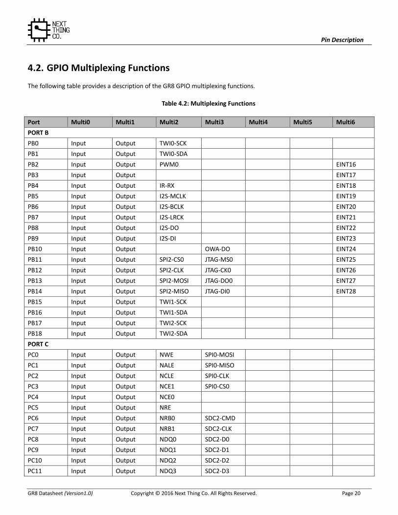
4.2. GPIO Multiplexing Functions
The following table provides a description of the GR8 GPIO multiplexing functions.
Table 4.2: Multiplexing Functions
Port Multi0 Multi1 Multi2 Multi3 Multi4 Multi5 Multi6
PORT B
PB0 Input Output TWI0-SCK
PB1 Input Output TWI0-SDA
PB2 Input Output PWM0 EINT16
PB3 Input Output EINT17
PB4 Input Output IR-RX EINT18
PB5 Input Output I2S-MCLK EINT19
PB6 Input Output I2S-BCLK EINT20
PB7 Input Output I2S-LRCK EINT21
PB8 Input Output I2S-DO EINT22
PB9 Input Output I2S-DI EINT23
PB10 Input Output OWA-DO EINT24
PB11 Input Output SPI2-CS0 JTAG-MS0 EINT25
PB12 Input Output SPI2-CLK JTAG-CK0 EINT26
PB13 Input Output SPI2-MOSI JTAG-DO0 EINT27
PB14 Input Output SPI2-MISO JTAG-DI0 EINT28
PB15 Input Output TWI1-SCK
PB16 Input Output TWI1-SDA
PB17 Input Output TWI2-SCK
PB18 Input Output TWI2-SDA
PORT C
PC0 Input Output NWE SPI0-MOSI
PC1 Input Output NALE SPI0-MISO
PC2 Input Output NCLE SPI0-CLK
PC3 Input Output NCE1 SPI0-CS0
PC4 Input Output NCE0
PC5 Input Output NRE
PC6 Input Output NRB0 SDC2-CMD
PC7 Input Output NRB1 SDC2-CLK
PC8 Input Output NDQ0 SDC2-D0
PC9 Input Output NDQ1 SDC2-D1
PC10 Input Output NDQ2 SDC2-D2
PC11 Input Output NDQ3 SDC2-D3
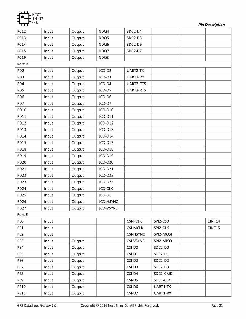
Pin Description
GR8 Datasheet (Version1.0) Copyright © 2016 Next Thing Co. All Rights Reserved. Page 21
PC12 Input Output NDQ4 SDC2-D4
PC13 Input Output NDQ5 SDC2-D5
PC14 Input Output NDQ6 SDC2-D6
PC15 Input Output NDQ7 SDC2-D7
PC19 Input Output NDQS
Port D
PD2 Input Output LCD-D2 UART2-TX
PD3 Input Output LCD-D3 UART2-RX
PD4 Input Output LCD-D4 UART2-CTS
PD5 Input Output LCD-D5 UART2-RTS
PD6 Input Output LCD-D6
PD7 Input Output LCD-D7
PD10 Input Output LCD-D10
PD11 Input Output LCD-D11
PD12 Input Output LCD-D12
PD13 Input Output LCD-D13
PD14 Input Output LCD-D14
PD15 Input Output LCD-D15
PD18 Input Output LCD-D18
PD19 Input Output LCD-D19
PD20 Input Output LCD-D20
PD21 Input Output LCD-D21
PD22 Input Output LCD-D22
PD23 Input Output LCD-D23
PD24 Input Output LCD-CLK
PD25 Input Output LCD-DE
PD26 Input Output LCD-HSYNC
PD27 Input Output LCD-VSYNC
Port E
PE0 Input CSI-PCLK SPI2-CS0 EINT14
PE1 Input CSI-MCLK SPI2-CLK EINT15
PE2 Input CSI-HSYNC SPI2-MOSI
PE3 Input Output CSI-VSYNC SPI2-MISO
PE4 Input Output CSI-D0 SDC2-D0
PE5 Input Output CSI-D1 SDC2-D1
PE6 Input Output CSI-D2 SDC2-D2
PE7 Input Output CSI-D3 SDC2-D3
PE8 Input Output CSI-D4 SDC2-CMD
PE9 Input Output CSI-D5 SDC2-CLK
PE10 Input Output CSI-D6 UART1-TX
PE11 Input Output CSI-D7 UART1-RX
Pin Description
GR8 Datasheet (Version1.0) Copyright © 2016 Next Thing Co. All Rights Reserved. Page 22
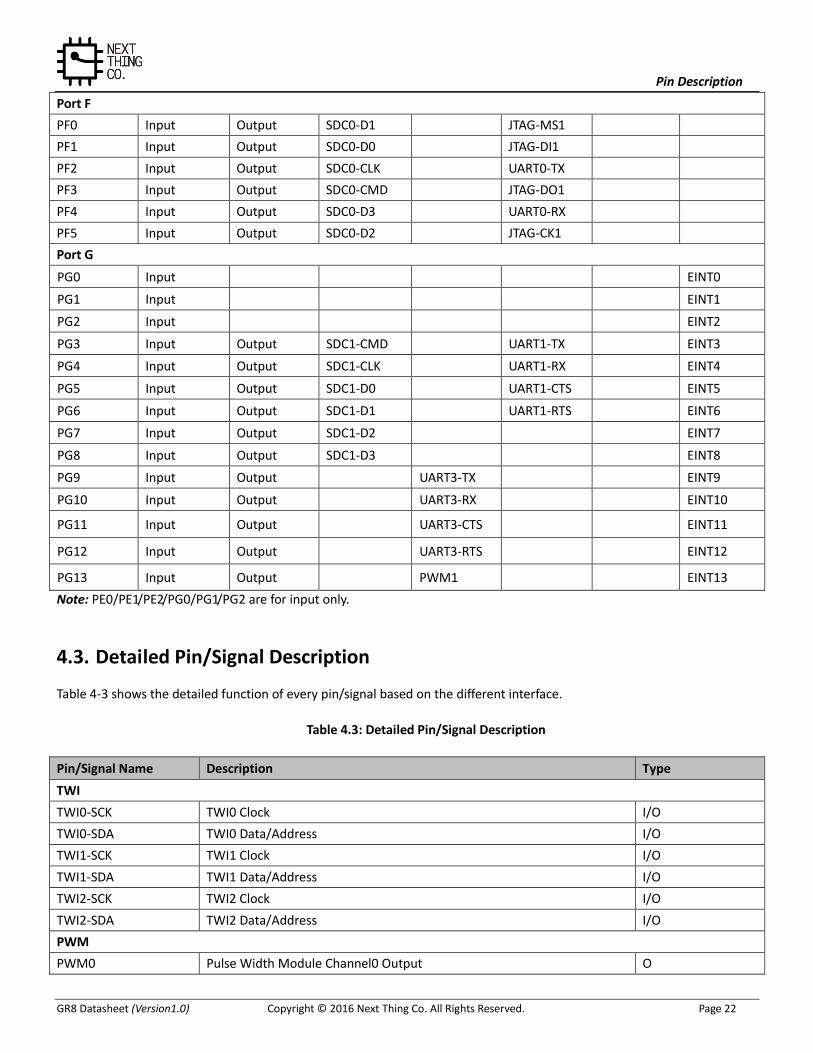
Port F
PF0 Input Output SDC0-D1 JTAG-MS1
PF1 Input Output SDC0-D0 JTAG-DI1
PF2 Input Output SDC0-CLK UART0-TX
PF3 Input Output SDC0-CMD JTAG-DO1
PF4 Input Output SDC0-D3 UART0-RX
PF5 Input Output SDC0-D2 JTAG-CK1
Port G
PG0 Input EINT0
PG1 Input EINT1
PG2 Input EINT2
PG3 Input Output SDC1-CMD UART1-TX EINT3
PG4 Input Output SDC1-CLK UART1-RX EINT4
PG5 Input Output SDC1-D0 UART1-CTS EINT5
PG6 Input Output SDC1-D1 UART1-RTS EINT6
PG7 Input Output SDC1-D2 EINT7
PG8 Input Output SDC1-D3 EINT8
PG9 Input Output UART3-TX EINT9
PG10 Input Output UART3-RX EINT10
PG11 Input Output UART3-CTS EINT11
PG12 Input Output UART3-RTS EINT12
PG13 Input Output PWM1 EINT13
Note: PE0/PE1/PE2/PG0/PG1/PG2 are for input only.
4.3. Detailed Pin/Signal Description
Table 4-3 shows the detailed function of every pin/signal based on the different interface.
Table 4.3: Detailed Pin/Signal Description
Pin/Signal Name Description Type
TWI
TWI0-SCK TWI0 Clock I/O
TWI0-SDA TWI0 Data/Address I/O
TWI1-SCK TWI1 Clock I/O
TWI1-SDA TWI1 Data/Address I/O
TWI2-SCK TWI2 Clock I/O
TWI2-SDA TWI2 Data/Address I/O
PWM
PWM0 Pulse Width Module Channel0 Output O
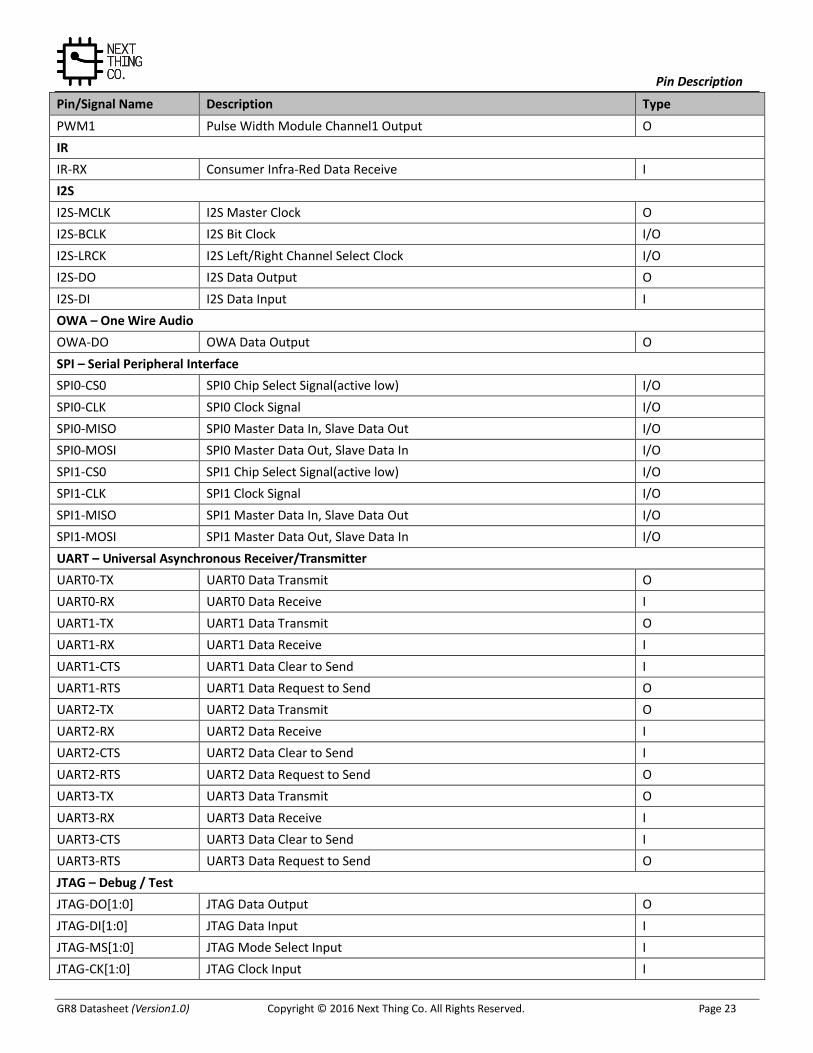
Pin Description
GR8 Datasheet (Version1.0) Copyright © 2016 Next Thing Co. All Rights Reserved. Page 23
Pin/Signal Name Description Type
PWM1 Pulse Width Module Channel1 Output O
IR
IR-RX Consumer Infra-Red Data Receive I
I2S
I2S-MCLK I2S Master Clock O
I2S-BCLK I2S Bit Clock I/O
I2S-LRCK I2S Left/Right Channel Select Clock I/O
I2S-DO I2S Data Output O
I2S-DI I2S Data Input I
OWA – One Wire Audio
OWA-DO OWA Data Output O
SPI – Serial Peripheral Interface
SPI0-CS0 SPI0 Chip Select Signal(active low) I/O
SPI0-CLK SPI0 Clock Signal I/O
SPI0-MISO SPI0 Master Data In, Slave Data Out I/O
SPI0-MOSI SPI0 Master Data Out, Slave Data In I/O
SPI1-CS0 SPI1 Chip Select Signal(active low) I/O
SPI1-CLK SPI1 Clock Signal I/O
SPI1-MISO SPI1 Master Data In, Slave Data Out I/O
SPI1-MOSI SPI1 Master Data Out, Slave Data In I/O
UART – Universal Asynchronous Receiver/Transmitter
UART0-TX UART0 Data Transmit O
UART0-RX UART0 Data Receive I
UART1-TX UART1 Data Transmit O
UART1-RX UART1 Data Receive I
UART1-CTS UART1 Data Clear to Send I
UART1-RTS UART1 Data Request to Send O
UART2-TX UART2 Data Transmit O
UART2-RX UART2 Data Receive I
UART2-CTS UART2 Data Clear to Send I
UART2-RTS UART2 Data Request to Send O
UART3-TX UART3 Data Transmit O
UART3-RX UART3 Data Receive I
UART3-CTS UART3 Data Clear to Send I
UART3-RTS UART3 Data Request to Send O
JTAG – Debug / Test
JTAG-DO[1:0] JTAG Data Output O
JTAG-DI[1:0] JTAG Data Input I
JTAG-MS[1:0] JTAG Mode Select Input I
JTAG-CK[1:0] JTAG Clock Input I
Pin Description
GR8 Datasheet (Version1.0) Copyright © 2016 Next Thing Co. All Rights Reserved. Page 24
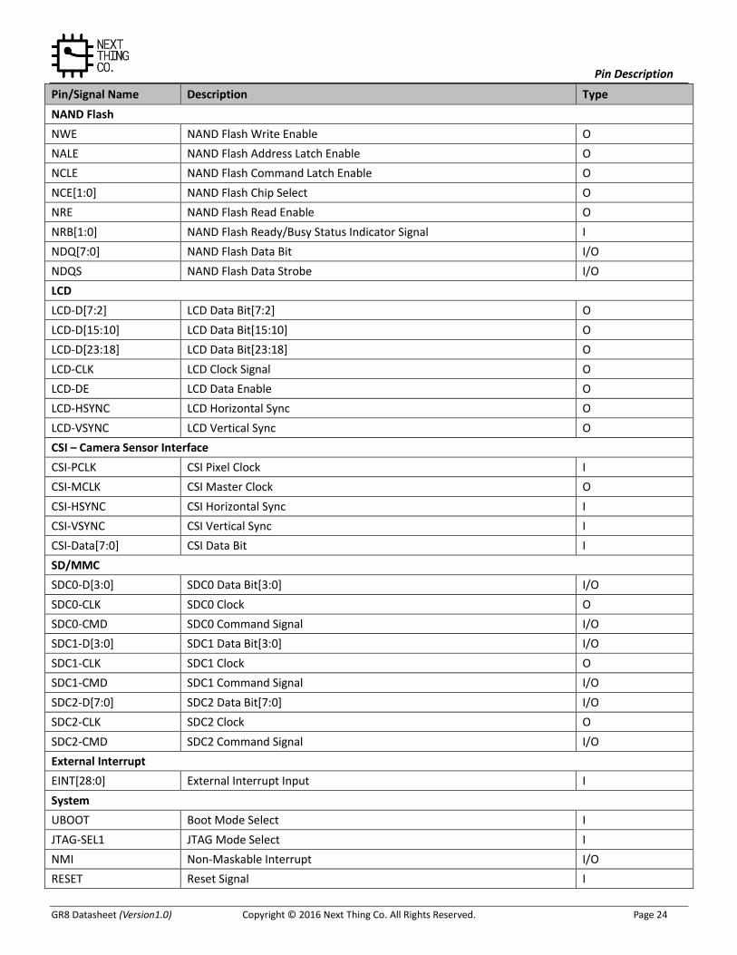
Pin/Signal Name Description Type
NAND Flash
NWE NAND Flash Write Enable O
NALE NAND Flash Address Latch Enable O
NCLE NAND Flash Command Latch Enable O
NCE[1:0] NAND Flash Chip Select O
NRE NAND Flash Read Enable O
NRB[1:0] NAND Flash Ready/Busy Status Indicator Signal I
NDQ[7:0] NAND Flash Data Bit I/O
NDQS NAND Flash Data Strobe I/O
LCD
LCD-D[7:2] LCD Data Bit[7:2] O
LCD-D[15:10] LCD Data Bit[15:10] O
LCD-D[23:18] LCD Data Bit[23:18] O
LCD-CLK LCD Clock Signal O
LCD-DE LCD Data Enable O
LCD-HSYNC LCD Horizontal Sync O
LCD-VSYNC LCD Vertical Sync O
CSI – Camera Sensor Interface
CSI-PCLK CSI Pixel Clock I
CSI-MCLK CSI Master Clock O
CSI-HSYNC CSI Horizontal Sync I
CSI-VSYNC CSI Vertical Sync I
CSI-Data[7:0] CSI Data Bit I
SD/MMC
SDC0-D[3:0] SDC0 Data Bit[3:0] I/O
SDC0-CLK SDC0 Clock O
SDC0-CMD SDC0 Command Signal I/O
SDC1-D[3:0] SDC1 Data Bit[3:0] I/O
SDC1-CLK SDC1 Clock O
SDC1-CMD SDC1 Command Signal I/O
SDC2-D[7:0] SDC2 Data Bit[7:0] I/O
SDC2-CLK SDC2 Clock O
SDC2-CMD SDC2 Command Signal I/O
External Interrupt
EINT[28:0] External Interrupt Input I
System
UBOOT Boot Mode Select I
JTAG-SEL1 JTAG Mode Select I
NMI Non-Maskable Interrupt I/O
RESET Reset Signal I
Pin Description
GR8 Datasheet (Version1.0) Copyright © 2016 Next Thing Co. All Rights Reserved. Page 25
Pin/Signal Name Description Type
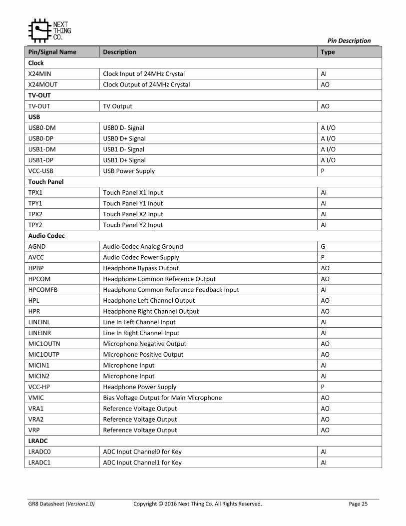
Clock
X24MIN Clock Input of 24MHz Crystal AI
X24MOUT Clock Output of 24MHz Crystal AO
TV-OUT
TV-OUT TV Output AO
USB
USB0-DM USB0 D- Signal A I/O
USB0-DP USB0 D+ Signal A I/O
USB1-DM USB1 D- Signal A I/O
USB1-DP USB1 D+ Signal A I/O
VCC-USB USB Power Supply P
Touch Panel
TPX1 Touch Panel X1 Input AI
TPY1 Touch Panel Y1 Input AI
TPX2 Touch Panel X2 Input AI
TPY2 Touch Panel Y2 Input AI
Audio Codec
AGND Audio Codec Analog Ground G
AVCC Audio Codec Power Supply P
HPBP Headphone Bypass Output AO
HPCOM Headphone Common Reference Output AO
HPCOMFB Headphone Common Reference Feedback Input AI
HPL Headphone Left Channel Output AO
HPR Headphone Right Channel Output AO
LINEINL Line In Left Channel Input AI
LINEINR Line In Right Channel Input AI
MIC1OUTN Microphone Negative Output AO
MIC1OUTP Microphone Positive Output AO
MICIN1 Microphone Input AI
MICIN2 Microphone Input AI
VCC-HP Headphone Power Supply P
VMIC Bias Voltage Output for Main Microphone AO
VRA1 Reference Voltage Output AO
VRA2 Reference Voltage Output AO
VRP Reference Voltage Output AO
LRADC
LRADC0 ADC Input Channel0 for Key AI
LRADC1 ADC Input Channel1 for Key AI
Electrical Characteristics
GR8 Datasheet (Version1.0) Copyright © 2016 Next Thing Co. All Rights Reserved. Page 26
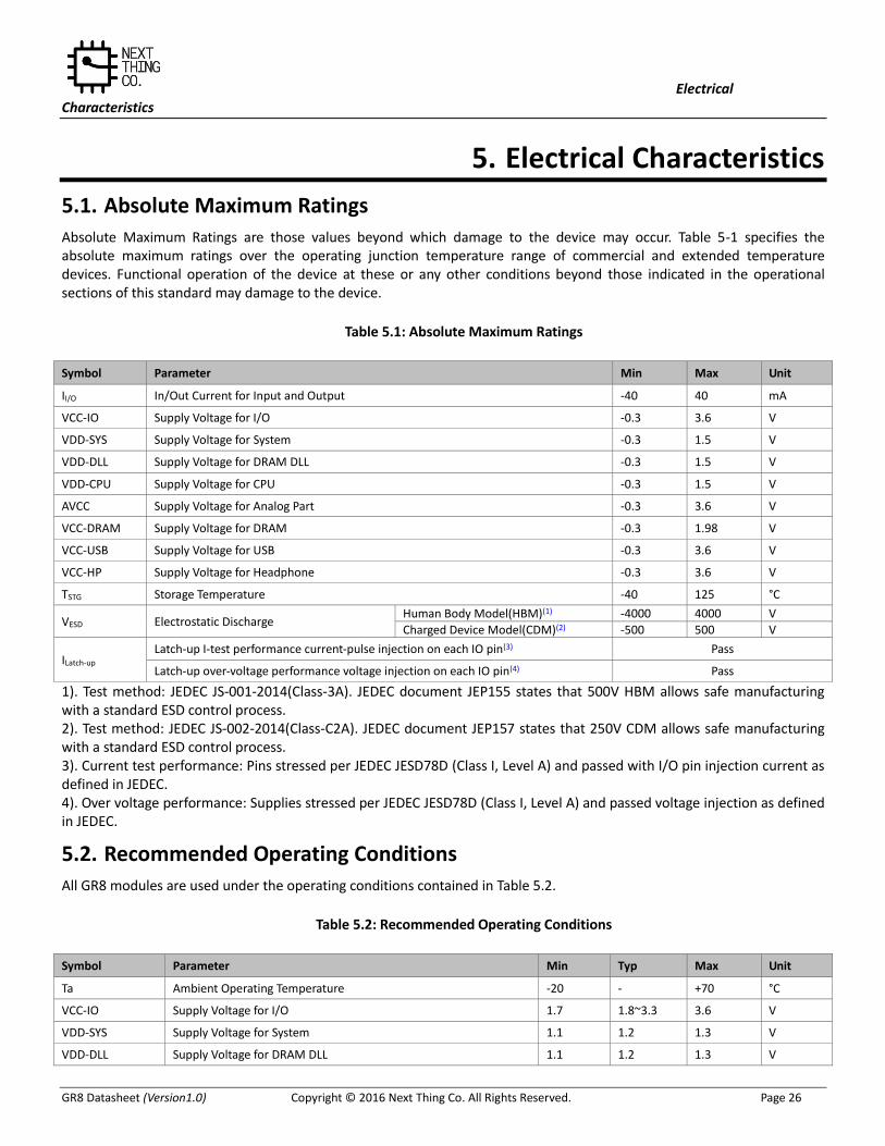
5. Electrical Characteristics
5.1. Absolute Maximum Ratings
Absolute Maximum Ratings are those values beyond which damage to the device may occur. Table 5-1 specifies the absolute maximum ratings over the operating junction temperature range of commercial and extended temperature devices. Functional operation of the device at these or any other conditions beyond those indicated in the operational sections of this standard may damage to the device.
Table 5.1: Absolute Maximum Ratings
Symbol Parameter Min Max Unit
II/O In/Out Current for Input and Output -40 40 mA
VCC-IO Supply Voltage for I/O -0.3 3.6 V
VDD-SYS Supply Voltage for System -0.3 1.5 V
VDD-DLL Supply Voltage for DRAM DLL -0.3 1.5 V
VDD-CPU Supply Voltage for CPU -0.3 1.5 V
AVCC Supply Voltage for Analog Part -0.3 3.6 V
VCC-DRAM Supply Voltage for DRAM -0.3 1.98 V
VCC-USB Supply Voltage for USB -0.3 3.6 V
VCC-HP Supply Voltage for Headphone -0.3 3.6 V
TSTG Storage Temperature -40 125 °C
VESD Electrostatic Discharge Human Body Model(HBM)(1) -4000 4000 V
Charged Device Model(CDM)(2) -500 500 V
ILatch-up Latch-up I-test performance current-pulse injection on each IO pin(3) Pass
Latch-up over-voltage performance voltage injection on each IO pin(4) Pass
1). Test method: JEDEC JS-001-2014(Class-3A). JEDEC document JEP155 states that 500V HBM allows safe manufacturing with a standard ESD control process. 2). Test method: JEDEC JS-002-2014(Class-C2A). JEDEC document JEP157 states that 250V CDM allows safe manufacturing with a standard ESD control process. 3). Current test performance: Pins stressed per JEDEC JESD78D (Class I, Level A) and passed with I/O pin injection current as defined in JEDEC. 4). Over voltage performance: Supplies stressed per JEDEC JESD78D (Class I, Level A) and passed voltage injection as defined in JEDEC.
5.2. Recommended Operating Conditions
All GR8 modules are used under the operating conditions contained in Table 5.2.
Table 5.2: Recommended Operating Conditions
Symbol Parameter Min Typ Max Unit
Ta Ambient Operating Temperature -20 - +70 °C
VCC-IO Supply Voltage for I/O 1.7 1.8~3.3 3.6 V
VDD-SYS Supply Voltage for System 1.1 1.2 1.3 V
VDD-DLL Supply Voltage for DRAM DLL 1.1 1.2 1.3 V
Electrical Characteristics
GR8 Datasheet (Version1.0) Copyright © 2016 Next Thing Co. All Rights Reserved. Page 27
VDD-CPU Supply Voltage for CPU 1.1 1.2 1.4 V
AVCC Supply Voltage for Analog Part - 3.0 - V
VCC-DRAM Supply Voltage for DRAM 1.425 1.5 1.575 V
VCC-USB Supply Voltage for USB 3.0 3.3 3.6 V
VCC-HP Supply Voltage for Headphone 3.0 - 3.3 V
5.3. DC Electrical Characteristics
Table 5.3 summarizes the DC electrical characteristics of GR8.
Table 5.3: DC Electrical Characteristics
Symbol Parameter Min Typ Max Unit
VIH High-Level Input Voltage 0.7 * VCC-IO - VCC-IO + 0.3 V
VIL Low-Level Input Voltage -0.3 - 0.3 * VCC-IO V
RPU Input Pull-up Resistance 50 100 150 KΩ
RPD Input Pull-down Resistance 50 100 150 KΩ
IIH High-Level Input Current - - 10 uA
IIL Low-Level Input Current - - 10 uA
VOH High-Level Output Voltage VCC-IO -0.2 - VCC-IO V
VOL Low-Level Output Voltage 0 - 0.2 V
IOZ Tri-State Output Leakage Current -10 - 10 uA
CIN Input Capacitance - - 5 pF
COUT Output Capacitance - - 5 pF
5.4. Oscillator Electrical Characteristics
GR8 contains one 24.000MHz oscillator.
The 24.000MHz frequency is used to generate the main source clock for PLL and the main digital blocks, the clock is provided through X24MIN. Table 5-4 lists the 24.000MHz crystal specifications.
Table 5.4: 24MHz Crystal Characteristics
Symbol Parameter Min Typ Max Unit
1/(tCPMAIN) Crystal Oscillator Frequency Range - 24.000 - MHz
tST Startup Time - - - ms
Frequency Tolerance at 25 °C -50 - +50 ppm
Oscillation Mode Fundamental –
Maximum Change Over Temperature Range -50 - +50 ppm
PON Drive Level - - 300 uW
CL Equivalent Load Capacitance 12 18 22 pF
RS Series Resistance(ESR) - 25 - Ω
Duty Cycle 30 50 70 %
Electrical Characteristics
GR8 Datasheet (Version1.0) Copyright © 2016 Next Thing Co. All Rights Reserved. Page 28
CM Motional Capacitance - - - pF
CSHUT Shunt Capacitance 5 6.5 7.5 pF
RBIAS Internal Bias Resistor 0.4 0.5 0.6 MΩ
5.5. Power Up/Down and Reset Specifications
The section provides information about the GR8 power up and power down sequence requirements.
5.5.1. Power Up Sequence Requirements
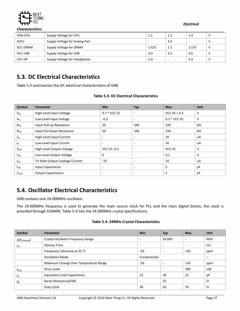
These requirements must be applied to meet the GR8 device power-up requirements (system power off to power on).
• Power up all domains simultaneously. • The RESET pin must be held on low until all power domains are stable.
Figure 5-1 shows the power up sequence.
Figure 5.1: Power Up Sequence
5.5.2. Power Up Reset Sequence Requirements
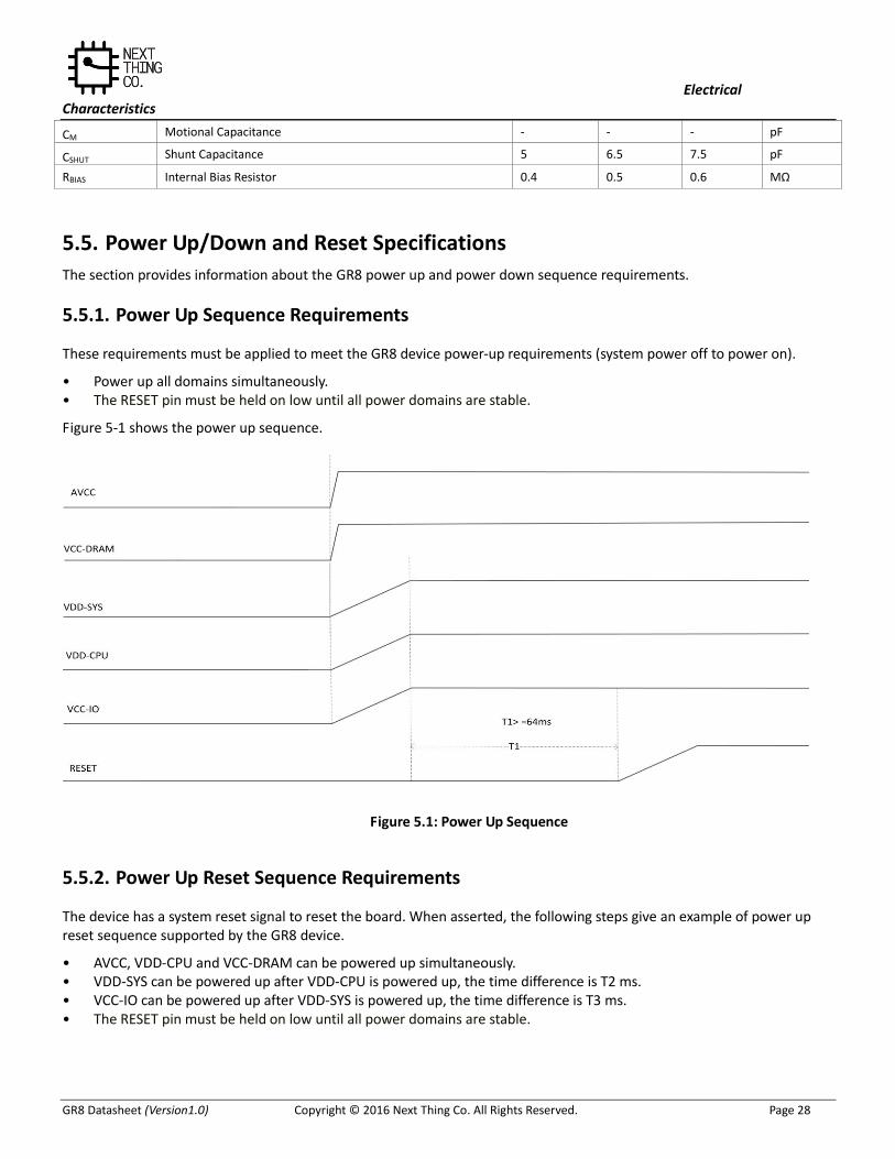
The device has a system reset signal to reset the board. When asserted, the following steps give an example of power up reset sequence supported by the GR8 device.
• AVCC, VDD-CPU and VCC-DRAM can be powered up simultaneously. • VDD-SYS can be powered up after VDD-CPU is powered up, the time difference is T2 ms. • VCC-IO can be powered up after VDD-SYS is powered up, the time difference is T3 ms. • The RESET pin must be held on low until all power domains are stable.
Electrical Characteristics
GR8 Datasheet (Version1.0) Copyright © 2016 Next Thing Co. All Rights Reserved. Page 29
Figure 5.2: Power Up Reset Sequence
5.5.3. Resume Power Up Sequence from Super Standby Mode
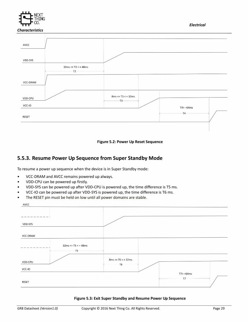
To resume a power up sequence when the device is in Super Standby mode:
• VCC-DRAM and AVCC remains powered up always. • VDD-CPU can be powered up firstly. • VDD-SYS can be powered up after VDD-CPU is powered up, the time difference is T5 ms. • VCC-IO can be powered up after VDD-SYS is powered up, the time difference is T6 ms. • The RESET pin must be held on low until all power domains are stable.
Figure 5.3: Exit Super Standby and Resume Power Up Sequence
Electrical Characteristics
GR8 Datasheet (Version1.0) Copyright © 2016 Next Thing Co. All Rights Reserved. Page 30
5.5.4. Power Down Sequence Requirements
To reduce power consumption, the GR8 can be partially powered down. The section lists the power down requirements in each mode. In Super Standby mode,
• VCC-DRAM and AVCC must be kept powered up. • VDD-CPU, VDD-SYS and VCC-IO are powered down simultaneously. • The falling time of VCC-IO is longest. The ramping down rate is decided by the load on the power supply.
VDD-CPU
AVCC
VCC-DRAM
VDD-SYS
VCC-IO
Figure 5.4: Power Down and Enter Super Standby Sequence
Figure 5-5 gives an example of the power-down sequence supported by the GR8 device.
• VDD-CPU, VDD-SYS and VCC-IO are powered down simultaneously. • VCC-DRAM and AVCC can be powered down after delay 16ms. • The falling time of VCC-IO is longest. The ramping down rate is decided by the load on the power supply.
VDD-CPU
AVCC
VCC-DRAM
VDD-SYS
VCC-IO
Figure 5.5: Power Down Sequence
Mechanical and Packaging Information
GR8 Datasheet (Version1.0) Copyright © 2016 Next Thing Co. All Rights Reserved. Page 31
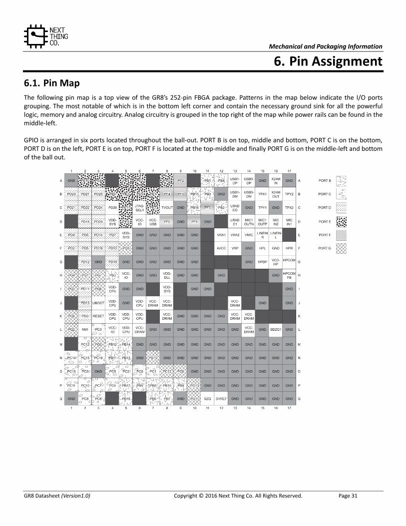
6. Pin Assignment
6.1. Pin Map
The following pin map is a top view of the GR8’s 252-pin FBGA package. Patterns in the map below indicate the I/O ports grouping. The most notable of which is in the bottom left corner and contain the necessary ground sink for all the powerful logic, memory and analog circuitry. Analog circuitry is grouped in the top right of the map while power rails can be found in the middle-left. GPIO is arranged in six ports located throughout the ball-out. PORT B is on top, middle and bottom, PORT C is on the bottom, PORT D is on the left, PORT E is on top, PORT F is located at the top-middle and finally PORT G is on the middle-left and bottom of the ball out.
Mechanical and Packaging Information
GR8 Datasheet (Version1.0) Copyright © 2016 Next Thing Co. All Rights Reserved. Page 32
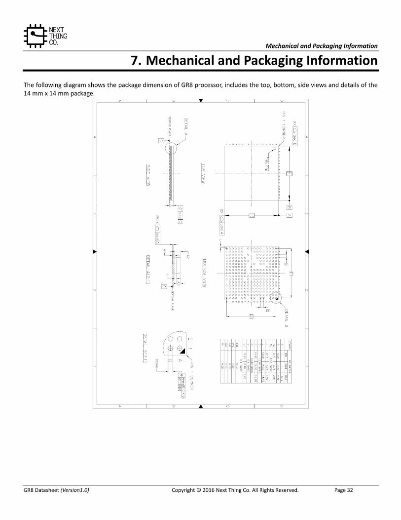
7. Mechanical and Packaging Information
The following diagram shows the package dimension of GR8 processor, includes the top, bottom, side views and details of the 14 mm x 14 mm package.
GR8 Datasheet (Version1.0) Copyright © 2016 Next Thing Co. All Rights Reserved. Page 33
Copyright © 2016 Next Thing Co. All Rights Reserved. Join the discussion @ http://bbs.nextthing.co/c/CHIP-Pro Contact Us Sales: [email protected] Technical Questions: [email protected] www.getchip.com