Embed Size (px)
Citation preview

Progress in Materials Science 56 (2011) 1178–1271
Contents lists available at ScienceDirect
Progress in Materials Science
journa l homepage : www.e lsev ie r .com/ loca te /pmatsc i
Graphene based materials: Past, present and future
Virendra Singh a,b, Daeha Joung a,c, Lei Zhai a,d,⇑, Soumen Das a,b,Saiful I. Khondaker a,c,e,⇑, Sudipta Seal a,b,⇑a Advanced Materials Processing Analysis Center and Nanoscience Technology Center, University of Central Florida, Orlando, FL, USAb Department of Mechanical, Materials and Aerospace Engineering, University of Central Florida, Orlando FL, USAc Department of Physics, University of Central Florida, Orlando, FL, USAd Department of Chemistry, University of Central Florida, Orlando, FL, USAe School of Electrical Engineering and Computer Science, University of Central Florida, Orlando, FL, USA
a r t i c l e i n f o
Article history:Received 22 February 2011Accepted 30 March 2011Available online 3 April 2011
0079-6425/$ - see front matter Published by Elsevdoi:10.1016/j.pmatsci.2011.03.003
⇑ Corresponding authors at: Advanced Materialsof Central Florida, Orlando, FL, USA.
E-mail addresses: [email protected] (L. Zhai), sai
a b s t r a c t
Graphene, a two dimensional monoatomic thick building block of acarbon allotrope, has emerged as an exotic material of the 21st cen-tury, and received world-wide attention due to its exceptionalcharge transport, thermal, optical, and mechanical properties.Graphene and its derivatives are being studied in nearly every fieldof science and engineering. Recent progress has shown that thegraphene-based materials can have a profound impact onelectronic and optoelectronic devices, chemical sensors, nanocom-posites and energy storage. The aim of this review article is toprovide a comprehensive scientific progress of graphene to dateand evaluate its future perspective. Various synthesis processes ofsingle layer graphene, graphene nanoribbons, chemically derivedgraphene, and graphene-based polymer and nano particle compos-ites are reviewed. Their structural, thermal, optical, and electricalproperties were also discussed along with their potential applica-tions. The article concludes with a brief discussion on the impact ofgraphene and related materials on the environment, its toxicologicaleffects and its future prospects in this rapidly emerging field.
Published by Elsevier Ltd.
Contents
1. Introduction . . . . . . . . . . . . . . . . . . . . . . . . . . . . . . . . . . . . . . . . . . . . . . . . . . . . . . . . . . . . . . . . . . . . . . . 11812. History of graphene . . . . . . . . . . . . . . . . . . . . . . . . . . . . . . . . . . . . . . . . . . . . . . . . . . . . . . . . . . . . . . . . . 1181
ier Ltd.
Processing Analysis Center and Nanoscience Technology Center, University
[email protected] (S.I. Khondaker), [email protected] (S. Seal).

V. Singh et al. / Progress in Materials Science 56 (2011) 1178–1271 1179
3. Synthesis of graphene . . . . . . . . . . . . . . . . . . . . . . . . . . . . . . . . . . . . . . . . . . . . . . . . . . . . . . . . . . . . . . . 1182
3.1. Exfoliation and cleavage . . . . . . . . . . . . . . . . . . . . . . . . . . . . . . . . . . . . . . . . . . . . . . . . . . . . . . . 11823.1.1. Mechanical exfoliation in solutions. . . . . . . . . . . . . . . . . . . . . . . . . . . . . . . . . . . . . . . . 11833.1.2. Intercalation of small molecules by mechanical exfoliation . . . . . . . . . . . . . . . . . . . . 1184
3.2. Chemical vapor deposition (CVD). . . . . . . . . . . . . . . . . . . . . . . . . . . . . . . . . . . . . . . . . . . . . . . . 1186
3.2.1. Thermal CVD. . . . . . . . . . . . . . . . . . . . . . . . . . . . . . . . . . . . . . . . . . . . . . . . . . . . . . . . . . 11863.2.2. Plasma enhanced CVD . . . . . . . . . . . . . . . . . . . . . . . . . . . . . . . . . . . . . . . . . . . . . . . . . . 11883.2.3. Thermal decomposition on SiC and other substrates . . . . . . . . . . . . . . . . . . . . . . . . . . 11883.3. Chemically derived graphene . . . . . . . . . . . . . . . . . . . . . . . . . . . . . . . . . . . . . . . . . . . . . . . . . . . 1188
3.3.1. Synthesis of graphene oxide and the reduction . . . . . . . . . . . . . . . . . . . . . . . . . . . . . . 11883.3.2. Surface functionalization of graphene oxide (GO) . . . . . . . . . . . . . . . . . . . . . . . . . . . . 11913.3.3. Structural and physical properties of reduced graphene oxide (RGO) . . . . . . . . . . . . 11923.4. Other synthesis approaches . . . . . . . . . . . . . . . . . . . . . . . . . . . . . . . . . . . . . . . . . . . . . . . . . . . . 1195
3.4.1. Total organic synthesis. . . . . . . . . . . . . . . . . . . . . . . . . . . . . . . . . . . . . . . . . . . . . . . . . . 11953.4.2. Un-zipping carbon nanotubes (CNTs) . . . . . . . . . . . . . . . . . . . . . . . . . . . . . . . . . . . . . . 11984. Graphene: characterization and properties . . . . . . . . . . . . . . . . . . . . . . . . . . . . . . . . . . . . . . . . . . . . . . 1201
4.1. Characterization . . . . . . . . . . . . . . . . . . . . . . . . . . . . . . . . . . . . . . . . . . . . . . . . . . . . . . . . . . . . . 12014.1.1. Optical imaging of graphene layers . . . . . . . . . . . . . . . . . . . . . . . . . . . . . . . . . . . . . . . . 12014.1.2. Fluorescence quenching technique . . . . . . . . . . . . . . . . . . . . . . . . . . . . . . . . . . . . . . . . 12014.1.3. Atomic force microscopy (AFM) . . . . . . . . . . . . . . . . . . . . . . . . . . . . . . . . . . . . . . . . . . 12034.1.4. Transmission electron microscopy (TEM) . . . . . . . . . . . . . . . . . . . . . . . . . . . . . . . . . . . 12044.1.5. Raman spectroscopy. . . . . . . . . . . . . . . . . . . . . . . . . . . . . . . . . . . . . . . . . . . . . . . . . . . . 1206
4.2. Properties. . . . . . . . . . . . . . . . . . . . . . . . . . . . . . . . . . . . . . . . . . . . . . . . . . . . . . . . . . . . . . . . . . . 1207
4.2.1. Electrical transport property . . . . . . . . . . . . . . . . . . . . . . . . . . . . . . . . . . . . . . . . . . . . . 12074.2.2. Quantum Hall effect . . . . . . . . . . . . . . . . . . . . . . . . . . . . . . . . . . . . . . . . . . . . . . . . . . . . 12114.2.3. Optical properties . . . . . . . . . . . . . . . . . . . . . . . . . . . . . . . . . . . . . . . . . . . . . . . . . . . . . . 12124.2.4. Mechanical properties . . . . . . . . . . . . . . . . . . . . . . . . . . . . . . . . . . . . . . . . . . . . . . . . . . 12144.2.5. Thermal properties . . . . . . . . . . . . . . . . . . . . . . . . . . . . . . . . . . . . . . . . . . . . . . . . . . . . . 12155. Chemically derived graphene: properties and applications. . . . . . . . . . . . . . . . . . . . . . . . . . . . . . . . . . 1216
5.1. Assembly of GO/RGO for device applications . . . . . . . . . . . . . . . . . . . . . . . . . . . . . . . . . . . . . . 12165.2. Electrical characterization of GO/RGO sheet . . . . . . . . . . . . . . . . . . . . . . . . . . . . . . . . . . . . . . . 12185.3. Defect density in chemically derived graphene. . . . . . . . . . . . . . . . . . . . . . . . . . . . . . . . . . . . . 12205.4. RGO as graphene quantum dot array: Coulomb blockade effect . . . . . . . . . . . . . . . . . . . . . . . 12215.5. Hopping conduction in RGO . . . . . . . . . . . . . . . . . . . . . . . . . . . . . . . . . . . . . . . . . . . . . . . . . . . . 12225.5.1. Mott variable range hopping . . . . . . . . . . . . . . . . . . . . . . . . . . . . . . . . . . . . . . . . . . . . . 12225.5.2. Efros–Shklovskii (ES) VRH . . . . . . . . . . . . . . . . . . . . . . . . . . . . . . . . . . . . . . . . . . . . . . . 1224
5.6. Application of RGO for photodetector, phototransistor and emitter . . . . . . . . . . . . . . . . . . . . 12245.7. Graphene thin film as transparent electrodes . . . . . . . . . . . . . . . . . . . . . . . . . . . . . . . . . . . . . . 12265.8. Solar cell using GO/RGO . . . . . . . . . . . . . . . . . . . . . . . . . . . . . . . . . . . . . . . . . . . . . . . . . . . . . . . 12285.9. Electrochemical sensors and biosensors . . . . . . . . . . . . . . . . . . . . . . . . . . . . . . . . . . . . . . . . . . 1230
6. Graphene based composites . . . . . . . . . . . . . . . . . . . . . . . . . . . . . . . . . . . . . . . . . . . . . . . . . . . . . . . . . . 1232
6.1. Graphene–polymer composites . . . . . . . . . . . . . . . . . . . . . . . . . . . . . . . . . . . . . . . . . . . . . . . . . 12326.1.1. Synthesis of graphene reinforced polymer composite . . . . . . . . . . . . . . . . . . . . . . . . . 12346.1.2. Mechanical properties . . . . . . . . . . . . . . . . . . . . . . . . . . . . . . . . . . . . . . . . . . . . . . . . . . 12366.1.3. Electrical properties . . . . . . . . . . . . . . . . . . . . . . . . . . . . . . . . . . . . . . . . . . . . . . . . . . . . 12386.1.4. Thermal conductivity . . . . . . . . . . . . . . . . . . . . . . . . . . . . . . . . . . . . . . . . . . . . . . . . . . . 12396.1.5. Other properties . . . . . . . . . . . . . . . . . . . . . . . . . . . . . . . . . . . . . . . . . . . . . . . . . . . . . . . 12406.1.6. Applications . . . . . . . . . . . . . . . . . . . . . . . . . . . . . . . . . . . . . . . . . . . . . . . . . . . . . . . . . . 1241
6.2. Graphene–nanoparticles composites . . . . . . . . . . . . . . . . . . . . . . . . . . . . . . . . . . . . . . . . . . . . . 1241
6.2.1. Synthesis . . . . . . . . . . . . . . . . . . . . . . . . . . . . . . . . . . . . . . . . . . . . . . . . . . . . . . . . . . . . . 12416.2.2. Applications . . . . . . . . . . . . . . . . . . . . . . . . . . . . . . . . . . . . . . . . . . . . . . . . . . . . . . . . . . 12457. Toxicity of graphene/graphene oxide/reduced graphene oxide. . . . . . . . . . . . . . . . . . . . . . . . . . . . . . . 12548. Future prospects. . . . . . . . . . . . . . . . . . . . . . . . . . . . . . . . . . . . . . . . . . . . . . . . . . . . . . . . . . . . . . . . . . . . 1258
Acknowledgements . . . . . . . . . . . . . . . . . . . . . . . . . . . . . . . . . . . . . . . . . . . . . . . . . . . . . . . . . . . . . . . . . 1259References . . . . . . . . . . . . . . . . . . . . . . . . . . . . . . . . . . . . . . . . . . . . . . . . . . . . . . . . . . . . . . . . . . . . . . . . 1259

Nomenclature
AcronymsAFM atomic force microscopyAPTS 3-aminopropyltriethoxysilaneATRP atom transfer radical polymerizationCB Coulomb blockadeCCG chemically converted grapheneCNT carbon nanotubeCRG chemically reduced graphene oxideCVD chemical vapor depositionDCC N,N-dicyclohexylcarbodiimideDGU density gradient ultracentrifugationDMF N,N-dimethylformamideDMSO dimethyl sulfoxideDP dirac pointEBL electron-beam lithographyECL electrogenerated chemiluminescenceEDC 1-ethyl-3-(3-dimethylaminopropyl)-carbodiimideFET field effect transistorsFQM fluorescence quenching microscopyGNR graphene nanoribbonGO graphene oxideGQD graphene quantum dotHATU 2-(7-aza-1H-benzotriazole-1-yl)-1,1,3,3-tetramethyluronium hexafluorophosphateHRTEM high resolution transmission electron microscopyITO indium tin oxideLB Langmir–BlodgettLED light emitting diodeMOSFET metal oxide semiconductor FETNMP N-methyl-2-pyrrolidoneNMR nuclear magnetic resonanceNPs nanoparticlesP3HT poly(3-hexylthiophene)PAH polyacyclic hydrocarbonsPAN PolyacrylonitrilePEN poly (ethylene-2,6-naphthalate)PET polyethylene terephthalatePECVD plasma enhanced chemical vapor depositionPL photoluminescencePMMA poly(methylmethacrylate)PS polystyrenePSS poly(sodium 4-styrenesulfonate)PU poly urethanePVA poly(vinyl alcohol)PVC poly(vinyl chloride)QD quantum dotQHE quantum Hall effectRGO reduced graphene oxideSC sodium cholateSEM scanning electron microscopeSLG single layer grapheneSTEM scanning transmission electron microscopySTM scanning tunneling microscopyTBA Tetrabutylamomium
1180 V. Singh et al. / Progress in Materials Science 56 (2011) 1178–1271

TEM transmission electron microscopyTHF tetrahydrofuranTRG thermally reduced graphene oxideTSCuPc tetrasulfonate salt of copper phthalocyanineVRH variable range hoppingXPS X-ray photoelectron spectroscopy
V. Singh et al. / Progress in Materials Science 56 (2011) 1178–1271 1181
1. Introduction
The 5th of October, 2010 was another beautiful day at Partin Elementary School in Oviedo. WhenKaleb, a 6 year old kindergartener, took out his pencil and started writing letters on a piece of paper,he did not realize that he was using a material that caught the attention of all scientific communitythat same day. The Nobel Prize in Physics 2010 was awarded to Andre Geim and Konstantin Novoselov‘‘for ground breaking experiments regarding the two-dimensional material graphene’’, a layer ofgraphite in the pencil. Graphene, one of the allotropes (carbon nanotube, fullerene, diamond) of ele-mental carbon, is a planar monolayer of carbon atoms arranged into a two-dimensional (2D) honey-comb lattice with a carbon–carbon bond length of 0.142 nm [1]. Electrons in graphene behave likemassless relativistic particles, which contribute to very peculiar properties such as an anomalousquantum Hall effect and the absence of localization [2,3]. Graphene [2] has demonstrated a varietyof intriguing properties including high electron mobility at room temperature (250,000 cm2/Vs)[4,5] exceptional thermal conductivity (5000 W m�1 K�1) [6] and superior mechanical properties withYoung’s modulus of 1 TPa [7]. Its potential applications include single molecule gas detection, trans-parent conducting electrodes, composites and energy storage devices such as supercapacitors and lith-ium ion batteries [7–20]. In addition, a distinct band gap can be generated as the dimension ofgraphene is reduced into narrow ribbons with a width of 1–2 nm, producing semiconductive graphenewith potential applications in transistors [8–10]. There is no doubt that graphene has risen as a shiningstar in the horizon on the path of the scientists’ searching for new materials for future electronic andcomposite industry. This review article narrates the brief history of graphene related research, andpresents the synthesis of graphene and its derivatives and various characterization techniques per-taining to 2D structure. Many extraordinary properties of graphene such as electrical, mechanical,anomalous quantum Hall effect, thermal, and optical are discussed. These properties have generatedtremendous interest among material researchers. The recent applications in various fields such as inlarge scale assembly and field effect devices, sensors, transparent electrodes, photodetectors, solarcells, energy storage devices, polymer composites, nanocomposites will be reviewed with a brief up-date on toxicology. The conclusion and outlook summarizes the research activities and presents thepossible future research directions.
2. History of graphene
Although the usage of graphite started 6000 years ago, when Marican in Europe used it to decoratepottery, the research about graphene, essentially an isolated single-atom plane of graphite, dates backto the 1960s when surprisingly higher basal-plane conductivity of graphite intercalation compoundswere discovered compared to that of the original graphite [11–13]. While the scientific communitywas excited about the discovery that might lead to a lighter, cheaper substitute for existing metal con-ductors, they were puzzled by the cause of the high conductivity of graphite intercalation compoundsand cautious about the future applications. The research of graphene has grown slowly in late 20thcentury with the hope to observe superior electrical properties from thin graphite or graphene layerswhile obtaining graphene was considered to be a formidable task in both theoretical and experimentalaspect. In the graphite intercalation systems, large molecules were inserted between atomic planes,generating isolated graphene layers in a three-dimensional matrix. The subsequent removal of the lar-ger molecules produced a mixture of stacked or scrolled graphene layers without the control of the

1182 V. Singh et al. / Progress in Materials Science 56 (2011) 1178–1271
structure. It was generally believed that, based on both theoretical calculation and experimentalobservation, 2D materials did not exist without a 3D base. AB initio calculations showed that a graph-ene sheet was thermodynamically unstable with respect to other fullerene structures if its size wasless than about 20 nm (‘‘graphene is the least stable structure until about 6000 atoms’’ and becomesthe most stable one (as within graphite) only for sizes larger than 24,000 carbon atoms) [14]. Variousattempts were made to synthesize graphene including using the same approach for the growth of car-bon nanotubes (producing graphite with 100 layers of graphene) [15], chemical vapor deposition onmetal surfaces (a few layers of graphene) [16,17], or the thermal decomposition of SiC [18]. Althoughthese approaches did not produce perfect monolayer graphene, the studies showed high-chargemobility of a few layers of graphene and the CVD approach has been optimized and become a majortechnique to produce graphene nowadays [19–21]. It was until 2004 that Andre Geim and KonstantinNovoselov used a method to isolate graphene, a method similar to what young Kaleb did, drawingwith a piece of graphite or peeling graphite with adhesive tape till the graphene is found. Such a ‘‘kin-dergartner’’ approach can provide high quality graphene with size in hundreds of microns [22]. Thesehigh quality graphene crystals realize the investigation of their amazing properties. Since then, the re-search of graphene including the control of the graphene layers on substrates, functionalizing graph-ene and exploring the applications of graphene has grown exponentially. As shown in Fig. 2.1, thenumber of publications on graphene (according to ISI Web of KnowledgeSM) increases dramaticallyafter 2004.
The term of ‘‘graphene’’ was recommended by the relevant IUPAC commission to replace the olderterm ‘‘graphite layers’’ that was unsuitable in the research of single carbon layer structure, because athree-dimensionally (3D) stacking structure is identified as ‘‘graphite’’. The recent definition of graph-ene can be given as a two-dimensional monolayer of carbon atoms, which is the basic building block ofgraphitic materials (i.e. fullerene, nanotube, graphite).
3. Synthesis of graphene
3.1. Exfoliation and cleavage
Recent studies showed that graphite nanoplatelets (GNP) or graphene could be used as a viable andinexpensive filler substitute for carbon nanotubes (CNT) [23] in nanocomposites owing to the
Fig. 2.1. Number of publications on graphene in past 20 years.

V. Singh et al. / Progress in Materials Science 56 (2011) 1178–1271 1183
excellent in-plane mechanical, structural, thermal and electrical properties of graphite [24]. It isobvious that these excellent properties are relevant at the nanoscale and the manufacture of the con-ducting nanocomposites is highly dependent on the exfoliation of the graphite down to single graph-ene sheet in the matrices. However, the challenge remained to achieve complete and homogeneousdispersion of individual graphene sheets in various solvents [25]. Like CNT and other nanomaterials,the key challenge in synthesis and processing of bulk-quantity graphene sheets is aggregation.Graphene, a one-atom-thick planar sheet of sp2-bonded carbon atoms densely packed in a honeycombcrystal lattice has very large specific surface area. Unless well separated from each other, graphenetends to form irreversible agglomerates or even restack to form graphite through Van der Waals inter-actions. The prevention of aggregation is essential for graphene sheets because most of their uniqueproperties are only associated with individual sheets.
3.1.1. Mechanical exfoliation in solutionsMechanical exfoliation is a simple peeling process where a commercially available highly oriented
pyrolytic graphite (HOPG) sheet was dry etched in oxygen plasma to many 5 lm deep mesa (Fig. 3.1).The mesa was then stuck onto a photoresist and peeled off layers by a scotch tape. The thin flakes lefton the photoresist were washed off in acetone and transferred to a silicon wafer. It was found thatthese thin flakes were composed of monolayer or a few layers of graphene. While the mechanical exfo-liation of graphene used by Geim and coworkers [22] led to numerous exciting discoveries of grapheneelectronic and mechanical properties, such approach is limited by its low production.
On the other hand, although chemical oxidation of graphite and the subsequent exfoliation providelarge amount of graphite oxide monolayer, the invasive chemical treatment inevitably generatesstructural defects as indicated by Raman spectroscopic studies [26,27]. These structural defects dis-rupted the electronic structure of graphene and change it to semiconductive. The subsequent chemicalreduction or thermal annealing (up to 1000 �C) are virtually impossible to regenerate the graphenestructures as indicated by XPS studies [28]. Therefore, physical exfoliation approaches are desirablewhere it is required to maintain the graphene structure. Blake et al. and Hernandez et al. have dem-onstrated that graphite could be exfoliated in N-methyl-pyrrolidone to produce defect-free monolayergraphene [29,30]. Such approach utilizes the similar surface energy of N-methyl-pyrrolidone andgraphene that facilitates the exfoliation. However, the disadvantage of this process is the high costof the solvent and the high boiling point of the solvent that makes the following graphene depositiondifficult. Lotya and coworkers have used a surfactant (sodium dodecylbenzene sulfonate, SDBS) toexfoliate graphite in water to produce graphene. The graphene monolayers are stabilized againstaggregation by a relatively large potential barrier caused by the Coulomb repulsion betweensurfactant-coated sheets. The dispersions are reasonably stable with larger flakes precipitating out
Fig. 3.1. Mechanical exfoliation of graphene using scotch tape from HOPG.

Fig. 3.2. (A) Schematic illustration of the graphene exfoliation process. Graphite flakes are combined with sodium cholate (SC)in aqueous solution. Horn-ultrasonication exfoliates few-layer graphene flakes that are encapsulated by SC micelles. (B)Photograph of 90 lg mL�1 graphene dispersion in SC 6 weeks after it was prepared. (C) Schematic illustrating an ordered SCmonolayer on graphene. (Reproduced with permission from [32].)
1184 V. Singh et al. / Progress in Materials Science 56 (2011) 1178–1271
over more than 6 weeks [31]. Similarly, Green and Hersam have used sodium cholate as a surfactant toexfoliate graphite and moved further to isolate the resultant graphene sheets with controlled thick-ness using density gradient ultracentrifugation (DGU) (Fig. 3.2). Since the exfoliation of the graphiteyielded a dispersion of monolayer graphene and graphite with a few layers of graphene which havedifferent buoyant density. DGU separations of such mixture produce graphene sheets with meanthicknesses that increase as a function of their buoyant density (Fig. 3.3) [32].
3.1.2. Intercalation of small molecules by mechanical exfoliationAgglomeration in graphite can be reduced appreciably by incorporating small molecules between
the layers of graphite or by non-covalently attaching molecules or polymers onto the sheets, generat-ing graphite intercalation compounds (GICs). In GICs, the graphite layers remains unaltered with guestmolecules located in the interlayer galleries. When the layers of graphite interact with the guest mol-ecules by charge transfer, the in-plane electrical conductivity generally increases but when the mol-ecules form covalent bonds with the graphite layers as in fluorides or oxides the conductivitydecreases as the conjugated sp2 system is disrupted. The first graphite intercalation compound,(GIC), or commonly known as expandable graphite was prepared by Schafhautl in 1841 while analyz-ing crystal flake of graphite in sulfuric acid solution. In the laboratory, flake graphite was subjected toshear intensive mechanical stirring with ultrasonic solvent in the ultrasonic cleaning bath at room

Fig. 3.3. (A) Photograph of a centrifuge tube following the first iteration of density gradient ultracentrifugation (DGU). Theconcentrated graphene was diluted by a factor of 40 to ensure that all graphene bands could be clearly resolved in thephotograph. Lines mark the positions of the sorted graphene fractions within the centrifuge tube. (B and C) Representative AFMimages of graphene deposited using fractions f4 (B) and f16 (C) onto SiO2. (D) Height profile of regions marked in panels B (bluecurve) and C (red curve) demonstrating the different thicknesses of graphene flakes obtained from different DGU fractions.(Reproduced with permission from [32].)
V. Singh et al. / Progress in Materials Science 56 (2011) 1178–1271 1185
temperature to prepare expandable graphite. Experimental conditions could be tuned by changingultrasonic solvent, ultrasonic power (nominal power of 500 W and 250 W) and ultrasonic time. Afterthe treatment, the mixture was washed thoroughly with water to neutrality and dried below 60 �C for60 min. The expandable graphite was then expanded at 900 �C to obtain the expanded graphite (EG).The choice of ultrasonic solvent depended on the oxidation ability and water content of the solvents,which affected the volume of expanded graphite. Acetic acid, acetic acid anhydride, concentrated sul-furic acid and hydrogen peroxide were the examples of few ultrasonic solvents. Among all those, con-centrated sulfuric acid had been proved to be the best ultrasonic solvent to provide optimumcondition for preparing the expandable graphite with ultrasound irradiation. Such sulfuric acid inter-calated graphite compound consisted of layers of hexagonal carbon structure within which H2SO4 wasintercalated. EG could be prepared either by oxidation with a chemical reagent or electrochemically inthe intercalating acid [33,34]. Graphite could expand up to a hundred times in volume at high temper-ature [35] due to the thermal expansion of the evolved gases trapped between the graphene sheets. Soit was reasonably assumed that oxidants and other molecules could enter in the interlayer space of EGmore easily compared to natural graphite. The influence of ultrasonic solvent and ultrasonic power onthe volume of expanded graphite could be analyzed from the data listed in Table 3.1.
Li et al. reported the exfoliation–reintercalation–expansion of graphite to produce high quality sin-gle layer graphene sheets stably suspended in organic solvents [36]. Commercial expandable graphitewas subjected to brief heating (60s) at 1000 �C in forming gas. It was then grounded with NaCl crystalsand reintercalated with oleum. The exfoliated graphite was then dispersed in N,N-dimethylformamide(DMF) and treated with tetrabutylamomium (TBA). TBA could insert into and increase the distance be-tween adjacent layers of graphite facilitating the separation of graphene sheets in surfactant solutions.The reintercalation and the rapid, brief heating of EG enabled the preparation of highly conductinggraphene sheets without functionalizing the graphite.

Table 3.1The influence of ultrasonic solvent and ultrasonic power on the volume of expanded graphite.
Ultrasonic power (W) Ultrasonic solvents Ultrasonic time (min) Expanded volume (ml/g)
500 Acetic acid 60 150500 Conc. sulfuric acid 60 500500 Alcohol 60 120500 Hydrogen peroxide 60 140250 Acetic acid 60 140250 Conc. sulfuric acid 60 380250 Alcohol 60 80250 Hydrogen peroxide 60 100
1186 V. Singh et al. / Progress in Materials Science 56 (2011) 1178–1271
3.2. Chemical vapor deposition (CVD)
3.2.1. Thermal CVDBesides mechanical exfoliation and chemical reduction methods to produce graphene sheets, sev-
eral promising approaches including epitaxial growth from SiC, and chemical vapor deposition (CVD)on metal surfaces have been reported. Among them, the CVD growth appears to be the most promisingtechnique for large-scale production of mono- or few-layer graphene films. Although the formation of‘‘monolayer graphite’’ was mentioned in early CVD studies on metal single crystals [37–39] the firstsuccessful synthesis of few-layer graphene films using CVD was reported in 2006 by Somani andcoworkers using camphor as the precursor on Ni foils [40]. This study opened up a new graphene syn-thesis route with several unsolved issues like controlling the number of layers, and minimizing thefolding of graphene. Since then, much progress has been made to obtain graphene layers on severaltypes of metal substrates with controlled thickness [26,41–47]. After a chemical etching of the metalsubstrate, the graphene layers detach and can be transferred to another substrate, providing highquality graphene layers without complicated mechanical or chemical treatments.
The growth mechanism of graphene on substrates with mediate-high carbon solubility (>0.1 atom-ic %) such as Co and Ni is through the diffusion of the carbon into the metal thin film at the growthtemperature and the subsequent precipitation of carbon out of the bulk metal to metal surface uponthe cooling [43,48]. A typical CVD process (i.e. using Ni as a substrate) involves dissolving carbon intothe nickel substrate followed by a precipitation of carbon on the substrate by cooling the nickel. The Nisubstrate is placed in a CVD chamber at a vacuum of 10�3 Torr and temperature below 1000 �C with adiluted hydrocarbon gas. The deposition process starts with the incorporation of a limited quantity ofcarbon atoms into the Ni substrate at relatively low temperature, similar to the carburization process.The subsequent rapid quenching of the substrate caused the incorporated carbon atoms to out-diffuseonto the surface of the Ni substrate and form graphene layers. Therefore, the thickness and crystallineordering of the precipitated carbon (graphene layers) is controlled by the cooling rate and the concen-tration of carbon dissolved in the nickel which is determined by the type and concentration of the car-bonaceous gas in the CVD, and the thickness of the nickel layer.
In contrast, the graphene growth on low carbon solubility (<0.001 atomic %) substrate like Cumainly happens on the surface through the four-step process described by Li and coworkers as follow-ing [49]:
1. Catalytic decomposition of methane on Cu to form CxHy upon the exposure of Cu to methane andhydrogen. In this process, the Cu surface is either undersaturated, saturated, or supersaturated withCxHy species, depending on the temperature, methane pressure, methane flow, and hydrogen par-tial pressure.
2. Formation of nuclei as a result of local supersaturation of CxHy where undersaturated Cu surfacedoes not form nuclear.
3. Nuclei grow to form graphene islands on Cu surface saturated, or supersaturated with CxHy species.4. Full Cu surface coverage by graphene under certain temperature (T), methane flow rate (JMe), and
methane partial pressure (PMe).

V. Singh et al. / Progress in Materials Science 56 (2011) 1178–1271 1187
If the amount of available CxHy on the exposed Cu surface is insufficient to expand the C to the is-land edges, the Cu surface is only partially covered with graphene islands. Otherwise, if there is alwaysenough methane to form sufficient CxHy to drive the reaction between the CxHy at the surface and theedges of graphene islands, graphene islands would grow until to connect neighboring islands and fullycover the Cu surface. With the understanding of the graphene growth mechanism, various approacheswere applied to control the graphene growth rate to obtain monolayer graphene. Lee and coworkershave used SiO2/Si substrates, coated with 300 nm thick Ni or 700 nm thick Cu to produce graphenelayers [47]. The average number of graphene layers grown on a Ni catalyst ranged from three to eight,depending on the reaction time and cooling rates. On the other hand, the mono- and bilayer graphenegrows predominantly on a Cu catalyst. The low solubility of carbon in Cu is believed to induce the self-limiting graphene growth process [44]. To prevent the formation of multilayer graphene on mediate-high carbon solubility (>0.1 atomic %) substrates such as Co and Ni, the thin layers of Ni of thicknessless than 300 nm were deposited on SiO2/Si substrates to produce graphene monolayer [43]. Recently,Bae and coworkers reported a roll-to-roll production of 30-inch. graphene films using the CVD ap-proach [50]. Their fabrication process including three steps after the synthesis of graphene on coppersubstrates: (i) adhesion of polymer supports to the graphene on the copper foil; (ii) etching of the cop-per layers; and (iii) release of the graphene layers and transfer onto a target substrate (Fig. 3.4). Theobtained graphene monolayer films have sheet resistances as low as �125 X/square with 97.4% opti-cal transmittance, and exhibit the half-integer quantum Hall effect, indicating their high quality. Inaddition, a layer-by-layer stacking of doped four-layer film has sheet resistance as low as �30 X/square with �90% transparency, demonstrating great potential to replace commercial transparentelectrodes such as indium tin oxides.
An interesting feature of the CVD approach to synthesize graphene is the possibility for substitu-tional doping by introducing other gases, such as NH3, during the growth [51–53]. The nitrogen atomscan be doped into graphene as ‘‘pyridinic’’, ‘‘graphitic’’ and ‘‘pyrrolic’’ forms. These nitrogen dopedgraphene (N-graphene) layers have demonstrated interesting properties. For example, Dai’s grouphave used nitrogen doped graphene for oxygen reduction in fuel cells where the N-graphene electrodedemonstrate a steady-state catalytic current to be calculated three times higher than the Pt/C elec-trode over a large potential range. The long-term stability, tolerance to crossover, and poison effectof the N-graphene electrode are also better than Pt/C for oxygen reduction in alkaline electrolyte[52]. Reddy and coworkers have reported that the reversible discharge capacitance of N-graphene
Fig. 3.4. (A) Schematic of the roll-based production of graphene films grown on a copper foil. The process includes adhesion ofpolymer supports, copper etching (rinsing) and dry transfer-printing on a target substrate. A wet-chemical doping can becarried out using a setup similar to that used for etching. (B) Roll-to-roll transfer of graphene films from a thermal release tapeto a PET film at 120 �C. (C) A transparent ultralarge-area graphene film transferred on a 35-in. PET sheet. (D) An assembledgraphene/PET touch panel showing outstanding flexibility. (Reproduced with permission from [50].)

1188 V. Singh et al. / Progress in Materials Science 56 (2011) 1178–1271
in lithium ion batteries is almost double compared to pristine graphene because the surface defectsinduced by nitrogen doping [53].
3.2.2. Plasma enhanced CVDPlasma enhanced chemical vapor deposition (PECVD) offers another route of graphene synthesis
at a lower temperature compared to thermal CVD. Thick graphite structures were observed duringthe fabrication of ‘‘nanostructured graphite-like carbon’’ using a dc discharge PECVD. The first reportof the production of mono- and few layer of graphene by PECVD involved a radio frequency PECVDsystem to synthesize graphene on a various substrates where graphene sheets were produced from agas mixture of 5–100% CH4 in H2 (total pressure 12 Pa), at 900 W power and 680 �C substrate tem-perature [54,55]. Since then, much effort have been devoted to understand the graphene growthmechanism and to optimize experimental conditions to control the thickness of graphene films[56–58]. The advantages of the plasma deposition include very short deposition time (<5 min)and a lower growth temperature of 650 �C compared to the thermal CVD approach (1000 �C). Thegrowth mechanism involved a balance between the graphene deposition through the surface diffu-sion of C-bearing growth species from precursor gas and etching caused by atomic hydrogen. Theverticality of the graphene sheets, produced through this method, is caused by the plasma electricfield direction [56,58].
3.2.3. Thermal decomposition on SiC and other substratesProducing graphite through ultrahigh vacuum (UHV) annealing of SiC surface has been an attrac-
tive approach especially for semiconductor industry because the products are obtained on SiC sub-strates and requires no transfer before processing devices [18,59–61]. When SiC substrate is heatedunder UHV, silicon atoms sublimate from the substrate. The removal of Si leaves surface carbon atomsto rearrange into graphene layers. The thickness of graphene layers depends on the annealing time andtemperature. The formation of ‘‘few-layer graphene’’ (FLG) typically requires few minutes annealing ofthe SiC surface at temperature around 1200 �C [62]. More recently, vapor phase annealing has beenused to produce FLG on SiC. At the expense of a higher temperature (typically 400 �C above UHV tem-perature), [63] this method leads to the formation of FLG on SiC with an improved thickness homoge-neity [64]. Although producing graphene on SiC substrates is attractive, several hurdles prevent thereal application. For example, control the thickness of graphene layers in the routine production oflarge area graphene is very challenging. Another uncertainty involves the different epitaxial growthpatterns on different SiC polar face (i.e. Si-face or C-face). Unusual rotational graphene stacking wereobserved in multilayers graphene grown on the C-face surface but not on Si-face surface. Such mis-match of graphene growth process has profound effects on the physical and electronic properties ofepitaxial graphene. On the C-face, the ‘‘twisted’’ interface leads to the decoupling between differentlayers of graphene, each of which behaves as a single layer [65]. However, the electronic propertiesof graphene multilayers on Si-face remains controversial [59]. Future investigation is required tounderstand the mechanisms of the growth processes. The third issue is to understand the relationshipbetween the structure and electronic properties of the interface layer between graphene and substrate[61].
The similar approach was applied to other metallic substrates to grow graphene layers. The (0001)faces of ruthenium (Ru) crystals were used under UHV to produce epitaxial graphene layers where avery sparse graphene nucleation at high temperatures allowed a linear dimensions growth of macro-scopic single-crystalline domains [66,67]. It was found that the first graphene layer coupled stronglyto the Ru substrate, while the second layer was free of the substrate interaction and had the similarelectronic structure to free-standing graphene. Other metal substrates including Ir, Ni, Co, and Pt havebeen employed to produce graphene layers and was nicely reviewed by Wintterlin and Bocquet [68].
3.3. Chemically derived graphene
3.3.1. Synthesis of graphene oxide and the reductionAt present, chemical conversion of graphite to graphene oxide has emerged to be a viable route to
afford graphene-based single sheets in considerable quantities [69–73]. Graphite oxide (GO) is usually

V. Singh et al. / Progress in Materials Science 56 (2011) 1178–1271 1189
synthesized through the oxidation of graphite using oxidants including concentrated sulfuric acid, ni-tric acid and potassium permanganate based on Hummers method [74]. Compared to pristine graph-ite, GO is heavily oxygenated bearing hydroxyl and epoxy groups on sp3 hybridized carbon on thebasal plane, in addition to carbonyl and carboxyl groups located at the sheet edges on sp2 hybridizedcarbon. Hence, GO is highly hydrophilic and readily exfoliated in water, yielding stable dispersion con-sisting mostly of single layered sheets (graphene oxide). It is important to note that although graphiteoxide and graphene oxide share similar chemical properties (i.e. surface functional group), their struc-tures are different. Graphene oxide is a monolayer material produced by the exfoliation of GO. Suffi-ciently dilute colloidal suspension of graphene oxide prepared by sonication are clear, homogeneousand stable indefinitely. AFM images of GO exfoliated by the ultrasonic treatment at concentrations of1 mg/ml in water always revealed the presence of sheets with uniform thickness (�1 nm). The pristinegraphite sheet is atomically flat with the Van der Waals thickness of �0.34 nm, graphene oxide sheetsare thicker due to the displacement of sp3 hybridized carbon atoms slightly above and below the ori-ginal graphene plane and presence of covalently bound oxygen atoms. A similar degree of exfoliationof GO was also attained for N,N-dimethylformamide (DMF), tetrahydrofuran (THF), N-methyl-2-pyrrolidone (NMP) and ethylene glycol [75]. Li et al. showed that the surface charges on grapheneoxide are highly negative when dispersed in water by measuring the zeta potential due to the ioniza-tion of the carboxylic acid and the phenolic hydroxyl groups [76]. Therefore, the formation of stablegraphene oxide colloids in water was attributed to not only its hydrophilicity but also the electrostaticrepulsion.
The chemical structure of graphene oxide such as the type and distribution of oxygen-containingfunctional groups have been studied using NMR 13C-labelled graphene oxide [77,78] suggesting thatthe basal plane of the sheet is decorated with hydroxyl and epoxy (1,2-ether) functional groups withsmall amount of lactol, ester, acid and ketone carbonyl groups at the edge. These results are in goodagreement with the model proposed by Lerf–Klinowski [79,80] and Dékány Models with small mod-ification [81]. These functional groups provide reactive sites for a variety of surface-modification reac-tions to develop functionalized graphene oxide- and graphene-based materials. On the other hand,due to the disruption of the conjugated electronic structure by these functional groups, grapheneoxide was electrically insulating and contained irreversible defects and disorders [26,82], but chemicalreduction of graphene oxide could partially restore its conductivity [26,82,83] at values orders of mag-nitude below that of pristine graphene.
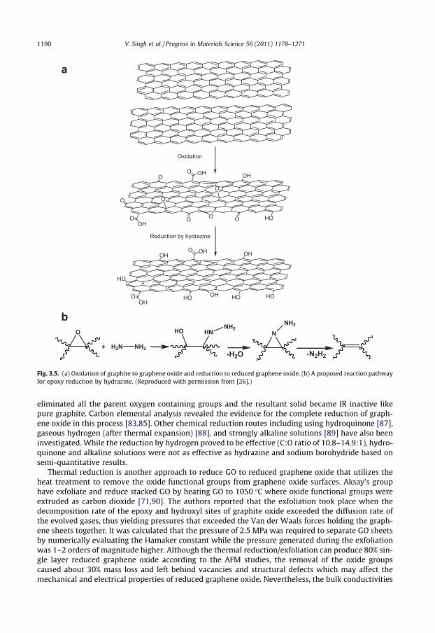
Chemical reduction of graphene oxide sheets has been performed with several reducing agentsincluding hydrazine [27,28,73,84], and sodium borohydrate [83,85]. Hydrazine hydrate, unlike otherstrong reductants, does not react with water and was found to be the best one in producing very thinand fine graphite-like sheets. During the reduction process, the brown colored dispersion of grapheneoxide in water turned black and the reduced sheets aggregated and precipitated [26,82]. The reducedgraphene oxide became less hydrophilic due to the removal of oxygen atoms and thus precipitated.The reason of re-establishment of the conjugated graphene network could be attributed to the reac-tion pathway proposed by Stankovich et al. (Fig. 3.5) [26]. Hydrazine takes part in ring-opening reac-tion with epoxides and forms hydrazino alcohols [86]. This initial derivative reacts further via theformation of an aminoaziridine moiety which undergoes thermal elimination of diimide to form adouble bond. Li and coworkers demonstrated the preparation of stable aqueous suspension of reducedgraphene oxide nanosheets by adjusting the pH (with ammonia solution) of the aqueous solution dur-ing reduction with hydrazine [76]. The carboxylic acid groups were unlikely to be reduced by hydra-zine and thus remained intact after hydroxyl reduction. The adjustment of pH with ammonia solutiondeprotonated the carboxylic acid groups and thus the electrostatic repulsion among the chargedgroups on reduced graphene oxide enabled the formation of well-dispersed graphene colloids in waterwithout any stabilizers. But, unless stabilized by selected surfactants, reduced graphene in organic sol-vent tend to agglomerate due to their hydrophobic nature [26,82]. Another possible route to reduceGO was using sodium borohydride (NaBH4) [83] in aqueous solution where sodium borohydride ismore effective than hydrazine as a reductant of graphene oxide although it can be slowly hydrolyzedby water. Such reduction produced reduced graphene oxide with sheet resistances as low as 59 kX/square (compared to 780 kX/square for a hydrazine reduced sample, measured in the same study),and C:O ratios were as high as 13.4:1 (compared to 6.2:1 for hydrazine). The NaBH4 treatment
O
O
OH
O
O O
O
OH
O
OH
HOO
O
O
HO
OH
OH
HO HO
OH OH
HOOH
O
Oxidation
Reduction by hydrazine
O
H2N NH2
HO HNNH2
NNH2
+-H2O -N2H2
a
b
Fig. 3.5. (a) Oxidation of graphite to graphene oxide and reduction to reduced graphene oxide. (b) A proposed reaction pathwayfor epoxy reduction by hydrazine. (Reproduced with permission from [26].)
1190 V. Singh et al. / Progress in Materials Science 56 (2011) 1178–1271
eliminated all the parent oxygen containing groups and the resultant solid became IR inactive likepure graphite. Carbon elemental analysis revealed the evidence for the complete reduction of graph-ene oxide in this process [83,85]. Other chemical reduction routes including using hydroquinone [87],gaseous hydrogen (after thermal expansion) [88], and strongly alkaline solutions [89] have also beeninvestigated. While the reduction by hydrogen proved to be effective (C:O ratio of 10.8–14.9:1), hydro-quinone and alkaline solutions were not as effective as hydrazine and sodium borohydride based onsemi-quantitative results.
Thermal reduction is another approach to reduce GO to reduced graphene oxide that utilizes theheat treatment to remove the oxide functional groups from graphene oxide surfaces. Aksay’s grouphave exfoliate and reduce stacked GO by heating GO to 1050 �C where oxide functional groups wereextruded as carbon dioxide [71,90]. The authors reported that the exfoliation took place when thedecomposition rate of the epoxy and hydroxyl sites of graphite oxide exceeded the diffusion rate ofthe evolved gases, thus yielding pressures that exceeded the Van der Waals forces holding the graph-ene sheets together. It was calculated that the pressure of 2.5 MPa was required to separate GO sheetsby numerically evaluating the Hamaker constant while the pressure generated during the exfoliationwas 1–2 orders of magnitude higher. Although the thermal reduction/exfoliation can produce 80% sin-gle layer reduced graphene oxide according to the AFM studies, the removal of the oxide groupscaused about 30% mass loss and left behind vacancies and structural defects which may affect themechanical and electrical properties of reduced graphene oxide. Nevertheless, the bulk conductivities

V. Singh et al. / Progress in Materials Science 56 (2011) 1178–1271 1191
of the products was measured to be 1000–2300 S/m, suggesting the effective reduction and restora-tion of electronic structures from GO [71]. Recently, Dubin et al. reported a simple one-step, solvother-mal reduction method to produce reduced graphene oxide dispersion in organic solvent [91]. Thedeoxygenation of GO resulted from both thermal deoxygenation at 200 �C when refluxing GO in N-methyl-2-pyrrolidinone (NMP) along with a concomitant reaction of GO with NMP molecules. Thesolvothermally reduced graphene oxide layers remained in a stable dispersion after the reaction.
This approach provides a simple, low-temperature method to produce reduced graphene oxide.
3.3.2. Surface functionalization of graphene oxide (GO)The surface functionalization of graphene oxide not only plays an important role in controlling
exfoliation behavior of graphene oxide and reduced graphene oxide but also holds the key to the gateleads to various applications. The surface functionalization has taken two approaches: covalent func-tionalization and non-covalent functionalization. In covalent functionalization, oxygen functionalgroups on graphene oxide surfaces, including carboxylic acid groups at the edge and epoxy/hydroxylgroups on the basal plane can be utilized to change the surface functionality of graphene oxide. Graph-ene oxide had been treated with organic isocyanates to give a number of chemically modified GO.Treatment of isocyanates reduced the hydrophilicity of graphene oxide by forming amide and carba-mate esters from the carboxyl and hydroxyl groups of graphene oxide, respectively. Consequently, iso-cyanate modified graphene oxide readily formed stable dispersion in polar aprotic solvents givingcompletely exfoliated single graphene sheets with thickness of �1 nm (Fig. 3.6). This dispersion alsofacilitated the intimate mixing of the graphene oxide sheets with matrix polymers, providing a novelsynthesis route to make graphene–polymer nanocomposites. Moreover, modified graphene oxide inthe suspension could be chemically reduced in presence of the host polymer to render electrical con-ductivity in the nanocomposites [92].
In order to use carboxylic acid groups on graphene oxide to anchor other molecules, the carboxylicacid groups have been activated by thionyl chloride (SOCl2) [93–96], 1-ethyl-3-(3-dimethylaminopro-pyl)- carbodiimide (EDC) [97], N,N-dicyclohexylcarbodiimide (DCC) [98], or 2-(7-aza-1H-benzotria-zole-1-yl)-1,1,3,3-tetramethyluronium hexafluorophosphate (HATU) [99]. The subsequent additionof nucleophilic species, such as amines or alcohols, produced covalently attached functional groups
O
O
OH
O
O O
O
OH
O
OH
HOO
O
RNCORNCO
O
O
NHR
O
O O
O
NHR
O
O
OCO2
ONHR
NHRO
Fig. 3.6. Isocyanate treatment of GO where organic isocyanate reacts with the hydroxyl and carboxyl groups of the grapheneoxide sheets.

1192 V. Singh et al. / Progress in Materials Science 56 (2011) 1178–1271
on graphene oxide via the formation of amides or esters. The resultant amine functionalized grapheneoxide has demonstrated various applications in optoelectronics [93,95,96], drug-delivery materials[97], biodevices [99], and polymer composites [98,100]. The attachment of hydrophobic long, aliphaticamine groups on hydrophilic graphene oxide improved the dispersability of modified graphene oxidein organic solvents [94], while porphyrin-functionalized primary amines and fullerene-functionalizedsecondary amines introduced interesting nonlinear optical properties [95,96]. The amine groups andhydroxyl groups on the basal plane of graphene oxide have also been used to attach polymers througheither grafting-onto or grafting-from approaches. To grow a polymer from graphene oxide, an atomtransfer radical polymerization (ATRP) initiator (i.e. a-bromoiobutyrylbromide) was attached tographene surfaces [101,102]. The following living polymerization produced graphene oxide with poly-mers that enhanced the compatibility of solvents and other polymer matrices. Besides the carboxylicacid groups, the epoxy groups on graphene oxide can be used to attach different functional groupsthrough a ring-opening reaction. Various amine ending chemicals such as octadecylamine [87], an io-nic liquid 1-(3-aminopropyl)-3-methylimidazolium bromide [96] with an amine end group and 3-aminopropyltriethoxysilane (APTS) have reacted with epoxy groups.
The non-covalent functionalization of graphene oxide utilizes the weak interactions (i.e. p–p inter-action, Van der Waals interactions and electrostatic interaction) between the graphene oxide and targetmolecules. The sp2 network on graphene oxide provides p–p interactions with conjugated polymersand aromatic compounds that can stabilize reduced graphene oxide resulted from chemical reductionand produce functional composite materials. The conjugated polymers and aromatic compoundsinclude poly(sodium 4-styrenesulfonate) (PSS) [82], sulfonated polyaniline [103], poly(3-hexylthiophene) (P3HT) [104], conjugated polyelectrolyte [105], 7,7,8,8-tetracyanoquinodimethaneanion [106], tetrasulfonate salt of copper phthalocyanine (TSCuPc) [107], porphyrin [108,109], pyreneand perylenediimide decorated with water-soluble moieties [110], and cellulose derivatives [111].During the chemical reduction of graphene oxide, reduced graphene oxide nanosheets are stabilizedvia the p–p interaction between aromatic molecules and reduced graphene oxide nanosheets. Aro-matic molecules have large aromatic plane and can anchor onto the reduced graphene oxide surfacewithout disturbing its electronic conjugation, providing stability for reduced graphene oxide. Forexample, the sulfonate groups on TSCuPc introduce negative charges on reduced graphene oxide sheetsand stabilize the RGO dispersion, providing single sheets of TSCuPc functionalized RGO for device fab-rication. In contrast, irreversible aggregation and precipitation of graphitic sheets occurred upon thereduction of graphene oxide without TSCuPc (Fig. 3.7B inset). Atomic force microscopy (AFM) study(Fig. 3.7) of reduced graphene oxide/TSCuPc composites provides detailed information about the indi-vidual layer of the reduced graphene oxide/TSCuPc composite sheets. The cross section analysis in theAFM height image indicates the thickness of the TSCuPc attached RGO sheet to be�1.9 nm whereas thethickness of a single layer RGO was found to be approximately 1 nm. Therefore, the AFM height imageconfirmed the non-covalent attachment of the aromatic molecules on the RGO basal plane through p–pinteraction. The small dots in the AFM images are aggregates of TSCuPc [107]. Dye-labeled DNA havealso been used to functionalize graphene oxide to detect proteins and DNA [112]. The fluorescenceof the dye on the reduced graphene oxide was quenched by the substrate. In the presence of a target,the binding between the dye-labeled DNA and target molecule will alter the conformation of dye-labeled DNA, and disturb the interaction between the dye-labeled DNA and graphene oxide. Such inter-actions will release the dye-labeled DNA from the GO, restoring of dye fluorescence.
3.3.3. Structural and physical properties of reduced graphene oxide (RGO)The optical and electrical properties of reduced graphene oxide depend on the spatial distribution
of the functional groups and structural defects. For example, the electron mean free path is limited bythe distance between two defective sites represented either by CAO or a vacancy [113]. A giant-infrared-absorption band was observed in reduced graphene oxide attributed to the coupling of elec-tronic states to the asymmetric stretch mode of a structure consisting of oxygen atoms aggregated atthe edges of defects [114]. Therefore, understanding the molecular structure evolution of the GOstructure during reduction is the key to obtain reduced graphene oxide with desired optical andelectrical properties. The structures of RGO have been studied both theoretically [115] and experimen-tally [78,114–118].

Fig. 3.7. Tapping mode AFM image of the RGO/TSCuPc composite on mica. Inset shows (A) Reducing of GO in the presence ofTSCuPc forms stable RGO/TSCuPc composite ink. (B) Precipitate formed when GO was reduced without TSCuPc.
V. Singh et al. / Progress in Materials Science 56 (2011) 1178–1271 1193
Bagri and coworkers used molecular dynamics (MD) simulation to study the atomic structure evo-lution from graphene oxide to RGO during the thermal annealing process [115]. As the author summa-rized in the paper, the carbonyl and ether groups on RGO formed from the hydroxyl and epoxy groupson graphene oxide during thermal annealing. Hydroxyl groups desorb at low temperature withoutaltering the graphene basal plane. In contrast, isolated epoxy groups are relatively more stable, andsubstantially distort the graphene lattice on desorption. The removal of carbon from the grapheneplane (generating structural defects) is more likely to occur when the initial hydroxyl and epoxygroups are close to each other. The reaction pathway during thermal annealing between two nearbyfunctional groups leads to the formation of carbonyl and ether groups, which are thermodynamicallyvery stable. These theoretical results are corroborated by FTIR spectroscopy and X-ray photoelectronspectroscopy (XPS) experiments.
A systematic investigation of the electrical and chemical structure evolution was performed on thereduction process via thermal treatment in UHV and in an Ar/H2 reducing atmosphere on pristine GOthin films and those that were previously treated with hydrazine vapor [116]. The progressive loss ofoxygen functional groups after each step of the reduction process was investigated by in situ XPS toreveal the change of carbon and oxygen bonds. It was found that the amount of carbon sp2 bondingincreased with the loss of oxygen during the annealing process, reaching a maximum value of�80% at an oxygen content of �8% (C:O ratio 12.5:1). This suggests that the remaining oxygen is

1194 V. Singh et al. / Progress in Materials Science 56 (2011) 1178–1271
responsible for �20% sp3 bonding and annealing up to 1100 �C is not sufficient to completely removethe oxygen from GO. Raman spectroscopy was also employed to reveal the structural evolution wherethe area ratio of the D and G bands was used as measure of the size of sp2 ring clusters in a network ofsp3 and sp2 bonded carbon. Using the empirical Tuinstra–Koenig relation [119] to obtain the lateraldimension of sp2 ring clusters, an average graphitic domain size of �2.5 nm in pristine GO was calcu-lated. After chemical (with hydrazine vapor) reduction and thermal annealing up to 500 �C, the changein the D/G peak area ratio was found to be negligible. A slight decrease in the full width half maxima(FWHM) of the D peak was observed only after annealing at 1100 �C, resulting in an increase in thesize of the sp2 cluster to �2.8 nm. This observation suggests that even when the sp2 carbon–carbonbonds are restored by de-oxidation, their spatial distribution in the honeycomb graphene lattice doesnot generate an expansion of a continuous sp2 phase. This may be due to the fact that the sp2 sites areisolated by disordered domains, which is indicated by the TEM studies [117,118]. The conductivitywas also measured vs. the sp2 fraction. The data indicated that the presence of residual oxygen(�8%) significantly hampered the carrier transport among the graphitic domains, and transport atthe initial stages of reduction was dominated by hopping or tunneling amongst the sp2 clusters. At lat-ter stages of reduction, newly formed smaller sp2 domains connected the original sp2 clusters so thatcharge could transport through percolation network. However, carrier transport above the percolationthreshold was limited by those clusters that are not perfect graphene crystals.
Erickson et al. have investigated the local chemical structures on graphene oxide and reducedgraphene oxide using the TEAM 0.5 TEM (a monochromated aberration-corrected instrument oper-ated at 80 keV) [117]. GO was produced via a modified Hummers method and drop cast onto laceycarbon TEM grids. For RGO specimens, GO-containing grids were reduced in a hydrazine atmosphereand then slowly heated to 550 �C under flowing N2. The TEM image of graphene oxide (Fig. 3.8) clearlyshows the oxidized area (A and B) and unoxidized graphene crystal area (Fig. 3.8c). As explained in thefigure caption, hydroxyl groups and epoxy were presented on the graphene oxide basal plane, in goodagreement with Lerf–Klinowski [79,80] and Dékány Models [81].
On the other hand, the TEM image of RGO shows the disordered regions (Fig. 3.9A) that are believedto result from the oxidized area being reduced by hydrazine and thermal annealing, and the unoxi-dized graphene regions.
Similarly, Gomez-Navarro and coworkers have used high resolution transmission electron micros-copy (HRTEM) to investigate the structure of reduced graphene oxide monolayers produced fromchemical oxidation/reduction of graphite in atomic scale. Defect free graphene domains with sizesof a few nanometers were mixed with defect areas dominated by clustered pentagons and heptagons[120]. The atomic structure of the RGO layers obtained from HRTEM is shown Fig. 3.10 with differentregions of the image marked by colors in Fig. 3.10b. The largest portion of the RGO layer is comprisedof clean well crystallized graphene areas where the hexagonal lattice is clearly observed (light graycolor in Fig. 3.10b). The average size of the visible well-crystallized areas is from 3 to 6 nm, covering�60% of the surface. The formation of larger holes is caused by electron irradiation, similar to the TEMimages of mechanically exfoliated graphene. In contrast to mechanically exfoliated graphene, RGO hasa large amount of topological defects within the clean areas. These defects was classified into isolatedtopological defects (pentagon–heptagon pairs, green), and extended (clustered) topological defectsthat appear as quasi-amorphous single layer carbon structures (marked in blue in Fig. 3.10b). The ex-tended topological defects cover ca. 5% of the surface and exhibit typical sizes of 1–2 nm in diameter.
According to the TEM studies, it is believed that isolated highly oxidized areas (few nm in size) areformed upon oxidation, while major graphene surface remains undisturbed. Upon reduction, the oxi-dized areas are restored to sp2-bonded carbon networks, which however lack the perfect crystallinityof intact graphene. The reduced disordered areas, which are best described as clustered topologicaldefects, induce strain as well as in-plane and out-of-plane deformations in the surrounding RGO. Iso-lated topological defects, mostly dislocations, are also present and may have formed as a result ofstrain. The effects of these defects will have to be taken into account for any comprehensive studyof the properties of RGO [120].
Gao et al. have investigated the structural change from graphene oxide to RGO using 13C NMR [78]. Intheir studies, RGO was produced from graphene oxide through a two-step reduction process—deoxygen-ation with NaBH4 (chemically converted graphene, CCG1), followed by dehydration with concentrated

Fig. 3.8. Aberration-corrected TEM image of a single sheet of suspended GO. The scale bar is 2 nm. Expansion (A) shows, fromleft to right, a 1 nm2 enlarged oxidized region of the material, then a proposed possible atomic structure of this region withcarbon atoms in gray and oxygen atoms in red, and finally the average of a simulated TEM image of the proposed structure and asimulated TEM image of another structure where the position of oxidative functionalities has been changed. Expansion (B)focuses on the white spot on the graphitic region. This spot moved along the graphitic region, but stayed stationary for threeframes (6 s) at a hydroxyl position (left portion of expansion (B)) and for seven frames (14 s) at a (1,2) epoxy position (rightportion of expansion (B)). The ball-and-stick figures below the microscopy images represent the proposed atomic structure forsuch functionalities. The simulated TEM image for the suggested structure agrees well with the TEM data. Expansion (C) showsa 1 nm2 graphitic portion from the exit plane wave reconstruction of a focal series of GO and the atomic structure of this region.(Reproduced with permission from [117].)
V. Singh et al. / Progress in Materials Science 56 (2011) 1178–1271 1195
sulfuric acid (CCG2) and annealing of CCG2 in Ar/H2 at 1100 �C for 15 min (CCG3). The authors suggestedthat this process produced graphene with a very low number of remaining functional groups, high con-ductivity, larger crystallite size and good solubility. The 13C NMR studies of graphene oxide illustratedthe functional groups, as discussed in previous section while the 13C NMR of different reduced materials,indicated that NaBH4 reduction removed the epoxy groups on the basal plane with the regeneration ofC@C bonds, the concentrated sulfuric acid treatment dehydrate hydroxyl groups to C@C bonds and thethermal annealing extrudes the carboxylic acid groups at the edge with the regeneration of C@C. By mea-suring the electric conductivity of the materials, the authors demonstrated the increased electrical con-ductivity (GO: 4.08 � 10�1 S/m, CCG1: 8.23 � 101 S/m, CCG2: 1.66 � 103 S/m, CCG3: 2.20 � 104 S/m)attributed to the restoration of conjugated electronic structures on RGO.
3.4. Other synthesis approaches
3.4.1. Total organic synthesisTotal synthesis of graphene-like polyacyclic hydrocarbons (PAHs), explored decades ago, has
caught much attention as a possible alternative route to synthesize graphene. Although PAHs havesome advantages including synthesis versatility and the capability of grafting aliphatic chains at theedge to modify solubility, the major challenge lies in preserving dispersibility and a planar geometryfor large PAHs. While different PAHs synthesis routes are nicely reviewed by Mullen et al. [121], it is

Fig. 3.9. Aberration-corrected TEM image of a monolayer of RGO. The scale bar is 1 nm. Expansion (A) shows, from left to right,an enlarged region of the micrograph, then a proposed possible structure for the region where oxygen (indicated in red) andnitrogen (blue) remain as functionalities on the sheets, and finally a simulated TEM image for this proposed structure.Expansion (B) shows the structure of a graphitic region. (Reproduced with permission from [117].)
1196 V. Singh et al. / Progress in Materials Science 56 (2011) 1178–1271
important to note that Mullen’s group has made a major break-through in synthesizing two-dimension graphene ribbons with the size of 12 nm through the Suzuki–Miyaura coupling of 1,4-diiodo-2,3,5,6-tetraphenylbenzene with 4-bromophenylboronic acid [122]. The same group recentlyreported a bottom-up method to fabricate graphene nanoribbons (GNR) on gold surfaces from10,100-dibromo-9,90-bianthryl precursor monomers [123]. In the fabrication process, thermal deposi-tion of the monomers onto a gold surface removes the halogen substituents from the precursors, andprovides the molecular building blocks for the targeted graphene ribbons (with a width of seven ben-zene molecules) in the form of surface-stabilized biradical species. During a first thermal activationstep, the biradical species diffuse across the surface and undergo radical addition reactions to form lin-ear polymer chains as imprinted by the specific chemical functionality pattern of the monomers. In asecond thermal activation step, a surface-assisted cyclodehydrogenation establishes an extended fullyaromatic system (Fig. 3.11).

Fig. 3.10. Atomic resolution, aberration-corrected TEM image of a single layer reduced graphene oxide membrane. (a) Originalimage and (b) with color added to highlight the different features. The defect free crystalline graphene area is displayed in theoriginal light gray color. Contaminated regions are shaded in dark gray. Blue regions are the disordered single-layer carbonnetworks, or extended topological defects, identified as remnants of the oxidation reduction process. Red areas highlightindividual ad-atoms or substitutions. Green areas indicate isolated topological defects, that is, single bond rotations ordislocation cores. Holes and their edge reconstructions are colored in yellow. Scale bar 1 nm. (Reproduced with permission from[120].)
Fig. 3.11. Bottom-up fabrication of atomically precise GNRs. Basic steps for surface-supported GNR synthesis, illustrated with aball-and-stick model of the example of 10,100-dibromo-9,90-bianthryl monomers (1). Grey, carbon; white, hydrogen; red,halogens; underlying surface atoms shown by large spheres. Top, dehalogenation during adsorption of the di-halogenfunctionalized precursor monomers. Middle, formation of linear polymers by covalent interlinking of the dehalogenatedintermediates. Bottom, formation of fully aromatic GNRs by cyclodehydrogenation. (Reproduced with permission from [123].)
V. Singh et al. / Progress in Materials Science 56 (2011) 1178–1271 1197

1198 V. Singh et al. / Progress in Materials Science 56 (2011) 1178–1271
The product of each reaction was monitored by scanning tunneling microscopy (STM) and thegraphene nanoribbon was characterized by Raman spectroscopy (Fig. 3.12). The STM image taken aftersurface assisted CAC coupling at 200 �C but before the final cyclodehydrogenation step shows a poly-anthrylene chain (Fig. 3.12b left) with a periodicity of 0.86 nm which is in good agreement with theperiodicity of the bianthry core of 0.85 nm. Fig. 3.12b, right shows a DFT-based simulation of theSTM image with partially overlaid model of the polymer (blue, carbon; white, hydrogen). The fullyaromatic system has an N = 7 armchair ribbon (Fig. 3.12c) with half the periodicity of the polymericchain (0.42 nm) and a markedly reduced apparent height of 0.18 nm. STM simulations are in perfectagreement with experimental images (Fig. 3.12e), confirming that the reaction products are atomicallyprecise N = 7 GNRs with fully hydrogen-terminated armchair edges. The peak at 396 cm�1 in Ramanspectrum is characteristic for the 0.74 nm width of the N = 7 ribbons. The inset in Fig. 3.12d showsthe atomic displacements characteristic for the radial-breathing like mode at 396 cm�1. In addition,the authors also demonstrated the fabrication of the straight N = 7 GNRs and the chevron-typeN = 6/N = 9 GNRs having been grown sequentially on a Ag(111) surface. These achievements suggestthat total synthesis is a versatile approach to make GNR with precise control of the composition andstructure. Studies on the electrical, optical and mechanical properties of these GNR are expected todirect interesting applications.
3.4.2. Un-zipping carbon nanotubes (CNTs)One of the graphene research goals is to introduce an energy band gap to realize the application in
semiconductor devices since pristine graphene is a zero-gap material. The graphene materials with anenergy gap can be produced through two approaches: controlled oxidation of a few layers of grapheneand fabrication GNR. Currently, it is very difficult to oxide a few layers of graphene in a controlled
Fig. 3.12. Straight GNRs from bianthryl monomers. (Reproduced with permission from [123].)
V. Singh et al. / Progress in Materials Science 56 (2011) 1178–1271 1199
manner. GNRs with narrow widths (<�10 nm) and atomically smooth edges, are predicted to haveband gaps useful for room temperature transistor operations with excellent switching speed and highcarrier mobility (potentially even ballistic transport) [124–127]. Yan et al. predicted that field effecttransistors (FETs) made from intrinsic semiconductor zigzag ribbons can exhibit very high levels ofperformance, with ON/OFF ratio up to 104, subthreshold swing as low as 60 meV per decade, andtransconductance of 9.5 � 103 S/m [127]. The most straight forward method to produce GNRs isthrough e-beam lithography which can generate wide GRNs with a width of 20 nm from graphenesheet. However, such approach is limited by poor scale resolution and large edge roughness [128].A chemical sonication route developed by Dai group produced sub-10 nm GNR semiconductors fromintercalated and exfoliated graphite but with low GNR yield and broad width distribution [8].
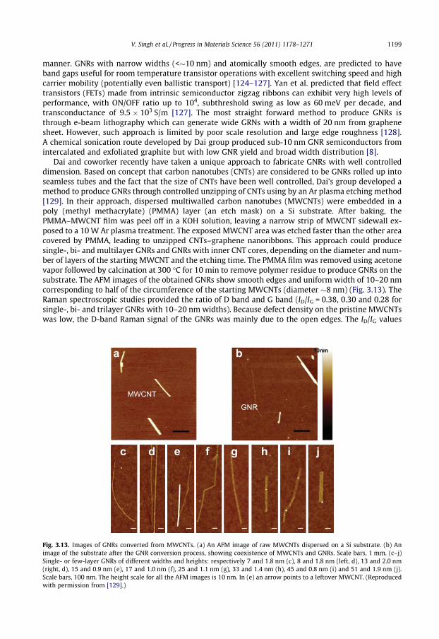
Dai and coworker recently have taken a unique approach to fabricate GNRs with well controlleddimension. Based on concept that carbon nanotubes (CNTs) are considered to be GNRs rolled up intoseamless tubes and the fact that the size of CNTs have been well controlled, Dai’s group developed amethod to produce GNRs through controlled unzipping of CNTs using by an Ar plasma etching method[129]. In their approach, dispersed multiwalled carbon nanotubes (MWCNTs) were embedded in apoly (methyl methacrylate) (PMMA) layer (an etch mask) on a Si substrate. After baking, thePMMA–MWCNT film was peel off in a KOH solution, leaving a narrow strip of MWCNT sidewall ex-posed to a 10 W Ar plasma treatment. The exposed MWCNT area was etched faster than the other areacovered by PMMA, leading to unzipped CNTs–graphene nanoribbons. This approach could producesingle-, bi- and multilayer GNRs and GNRs with inner CNT cores, depending on the diameter and num-ber of layers of the starting MWCNT and the etching time. The PMMA film was removed using acetonevapor followed by calcination at 300 �C for 10 min to remove polymer residue to produce GNRs on thesubstrate. The AFM images of the obtained GNRs show smooth edges and uniform width of 10–20 nmcorresponding to half of the circumference of the starting MWCNTs (diameter �8 nm) (Fig. 3.13). TheRaman spectroscopic studies provided the ratio of D band and G band (ID/IG = 0.38, 0.30 and 0.28 forsingle-, bi- and trilayer GNRs with 10–20 nm widths). Because defect density on the pristine MWCNTswas low, the D-band Raman signal of the GNRs was mainly due to the open edges. The ID/IG values
a b
c d e f g h i j
MWCNT
10nm
GNR
Fig. 3.13. Images of GNRs converted from MWCNTs. (a) An AFM image of raw MWCNTs dispersed on a Si substrate. (b) Animage of the substrate after the GNR conversion process, showing coexistence of MWCNTs and GNRs. Scale bars, 1 mm. (c–j)Single- or few-layer GNRs of different widths and heights: respectively 7 and 1.8 nm (c), 8 and 1.8 nm (left, d), 13 and 2.0 nm(right, d), 15 and 0.9 nm (e), 17 and 1.0 nm (f), 25 and 1.1 nm (g), 33 and 1.4 nm (h), 45 and 0.8 nm (i) and 51 and 1.9 nm (j).Scale bars, 100 nm. The height scale for all the AFM images is 10 nm. In (e) an arrow points to a leftover MWCNT. (Reproducedwith permission from [129].)

1200 V. Singh et al. / Progress in Materials Science 56 (2011) 1178–1271
were lower than those for GNRs obtained by lithographic etching of pristine graphene sheets (ID/IG � 2for a bilayer GNR of 28 nm width obtained by lithographic patterning), indicating the high quality ofthe GNRs obtained through this approach.
On the other hand, the electrical properties of the fabricated FET devices using these GNRs were notas good as the predicted value. A 7 nm-wide GNR device had an Ion/Ioff ratio of >10 and a 6 nm-wideGNR device had Ion/Ioff > 100. These GNRs had quantum-confined semiconducting characteristics,rather than those of bulk graphene, with much weaker gate modulation of conductance. The mobilityof the GNRs was similar to those fabricated by lithography with values 10 times lower than those oflarge two-dimensional graphene sheets, most likely because of the edge scattering in the GNRs.
Shimizu and coworkers produced GNRs through the oxidization and longitudinal unzipping ofMWCNTs in concentrated sulphuric acid, followed by treatment with KMnO4 (Fig. 3.14) [130]. The oxi-dative unzipping generated the graphene nanoribbons that are initially oxidized. The authors used athree-step annealing treatment to completely remove the oxygen from the bulk and edges of thenanoribbons and also effectively dope charge carriers. The first step annealed freshly deposited nano-ribbons on substrates at 800 �C to remove the bulk of the oxygenation. The second step was carriedout at 750 �C in a H2 atmosphere to produce edge termination and charge carrier doping before thefabrication of the FET electrodes using electron-beam lithography (EBL). The third step, annealingwas performed at 300 �C to clean the surface immediately before the formation of the electrodes.The obtained GNRs were examined by AFM, HRTEM and Raman Spectroscopy. The AFM height anal-ysis of monolayer GNRs showed a thickness of 0.8 nm while the HRTEM studies indicated the presenceof small amount of structural defects associated with the oxidation and uncompleted removal of oxi-dized groups which was supported by the investigation of electrical properties. The ratio of D bandand G band (ID/IG) was found to be �0.45, suggesting a good quality of the obtained GNRs.
Although the GNRs, obtained by various new unzipping methods [130–136], have inferior elec-tronic properties compared to those of wide, mechanically peeled sheets of graphene, these pioneerwork has paved a way leading to a large-scale production of GNRs with controlled structure and qual-ity and tunable properties. The future research will focus on understanding the mechanism of the pro-cess and optimizing the experimental parameters to prepare highly ordered sub-10 nm GNRs forpotential applications in room temperature transistors.
AB
Fig. 3.14. (A) Field-emission SEM image of an ensemble of the as-grown nanoribbons, which were dispersed on a SiO2 substratein a water droplet containing a suspension of nanoribbons. The nanoribbons are entangled and not sufficiently exfoliated. Inset(right): AFM images of individual nanoribbons spread by applying a strong air flow to the droplet. Inset (left): height of thenanoribbon measured along the longitudinal direction. The thickness of �0.8 nm indicates a single-layer nanoribbon. (B) FETfabricated using a nanoribbon end-bonded by two metal electrodes, which eliminates single-electron charging effects. Thethickness of the SiO2 layer on the gold/titanium backgate electrode was 300 nm, and the spacing of source and drain electrodeswas 500 nm in all samples. (Reproduced with permission from [130].)

V. Singh et al. / Progress in Materials Science 56 (2011) 1178–1271 1201
4. Graphene: characterization and properties
4.1. Characterization
4.1.1. Optical imaging of graphene layersVarious techniques are being used to image single layers, bi-layers and few layers of graphene such
as optical microscope, atomic force microscopy (AFM), scanning electron microscopy (SEM) and highresolution transmission electron microscopy (TEM). Often, a combination of two or more techniquescompletes imaging of different layers of graphene. After the discovery of graphene, the optical micro-scope was primarily used to image various layers since it is the cheapest, non-destructive, and readilyavailable in laboratories. However, this requires graphene layers mounting on silicon dioxide sub-strate for good contrast imaging. Over the past few years, the substrate designing has been given aconsiderable attention to enhance the visibility of thin sheets [137–139]. The mechanism behind suchcontrast is explained in terms of Fabry–Perot interference in the dielectric surface layer that governsthe fluorescence intensity that allows contrast between graphene layers and substrate. The visibility ofsheets can be defined by the Michelson contrast (C) relation [140]:
C ¼ Rmaterial � Rdielectric
Rmaterial þ Rdielectricð4:1Þ
where Rmaterial is the reflected intensity from the material and Rdielectric is the intensity without thematerial. If C = 0, the material is not detectable, C = 0 to +1 material is brighter than the substrate,and C = 0 to �1 the sample will be darker than the substrate.
SiO2 and Si3N4 are the most commonly overlay materials on silicon for enhancing the contrast ofgraphene layers which are dielectric in nature [141]. Another governing factor that modulates contrastis the wavelength of the incident light. Blake et al. [141] demonstrated the contact variation using dif-ferent narrow band filters to detect sheets for any thickness of SiO2 support. They found that undernormal white light illumination sheets were invisible on 200 nm SiO2, while thick and thin sheetswere visible on 300 nm SiO2 when green light was used, whereas sheets were visible on 200 nmSiO2 by blue light.
Fig. 4.1 shows the optical image of the different layers of the micromechanically exfoliated graph-ene on silicon substrate with 300 nm SiO2 over-layer. The number of layers was identified by colorcontrast and AFM [142]. So far the detection technique demonstrated is dependent on the substratethickness and incident light wavelength. More research is needed to facilitate graphene-based sheetsvisualization independent of support material without any modification of the graphene.
4.1.2. Fluorescence quenching techniqueRecently, a fluorescence quenching microscopy (FQM) technique was used to image graphene,
RGO and GO for immediate sample evaluation and manipulation so that the synthesis process canbe improved [143]. They have demonstrated the low cost and time saving method of visualizingGO and RGO using substrate independent fluorescence quenching microscopy (FQM). The imagingmechanism involves quenching the emission from a dye coated GO and RGO; the dye can be re-moved by rinsing without disrupting the sheets. The contrast arises due to the chemical interactionbetween the GO and the dye molecule on the molecular scale because of the charge transfer fromdye molecule to GO that causes quenching of fluorescence [144]. The contrast measured in the fluo-rescence images was achieved 0.78 for 300 nm SiOx layer. Furthermore, higher contrast wasachieved when GO sheets were deposited on 100 nm SiOx, quartz and glass substrates which gavethe contrast �0.52, 0.2 and 0.07 respectively. These values were sufficient for a clear visualization[144]. The image obtained by FQM is shown in Fig. 4.2 and compared to the AFM image of the samearea. The technique has the capability to see the microstructures of the GO/RGO film even on plasticsubstrate. However, this technique is limited to the micron sized layers because it is based on light,and the lateral resolution of FQM is diffraction limited. This technique relies on dye addition ongraphene surface, which prohibits further use of the same sample due to the attachment of un-wanted functional groups.

Fig. 4.1. Optical microscopy image of single-, double- and triple- layer graphene on Si with a 300 nm SiO2 over-layer, labeled inthe paper as 1L, 2L and 3L, respectively. (Reproduced with permission from [142].)
Fig. 4.2. (A) AFM image showing G-O single layers deposited on a SiO2/Si wafer before applying a 30 nm thick fluorescein/PVPlayer for FQM. (B) A FQM image of the same area of the wafer, showing good correlation to the AFM view. (C) After washing offthe dye coating, no residues can be detected by AFM. (D) Line scan data on a folded sheet show no significant deviation inthickness before and after FQM imaging (all scale bars �10 lm). (Reproduced with permission from [143].)
1202 V. Singh et al. / Progress in Materials Science 56 (2011) 1178–1271

V. Singh et al. / Progress in Materials Science 56 (2011) 1178–1271 1203
4.1.3. Atomic force microscopy (AFM)This technique of imaging can successfully determine the layer thickness at the nanometer scale.
However, this is cumbersome for imaging large area graphene. Moreover, AFM imaging gives onlytopographic contrast, which cannot distinguish between the graphene oxide and the graphene layersin normal operation. However, phase imaging is one of the attractive features of tapping-mode AFM;this facilitates to distinguish between a defect free pristine graphene and its functionalized version.One of the reasons behind is the difference in the interaction forces between the AFM tip and the at-tached functional group. Paredes et al. [145] demonstrated the influence of attractive mode of AFM todetermine the thickness of the sheet. They found that the repulsive mode induces deformation causingerror in the height measurement. They observed thickness �1.0 nm for the unreduced graphene oxideand 0.6 nm for the chemically reduced GO. The difference in the thickness and the phase contrast wasreported due to hydrophilicity difference resulting from distinct oxygen functional group in the reduc-tion process as shown in Fig. 4.3. Besides imaging and thickness detection, AFM has been explored formechanical characterization of graphene as it can resolve the small forces involved in the deformation
Fig. 4.3. Height (a and c) and corresponding phase (b and d) tapping-mode AFM images of unreduced (a and b) and chemicallyreduced (c and d) graphene oxide nanosheets deposited from aqueous dispersions onto freshly cleaved HOPG. The images wererecorded in the attractive regime of tip sample interaction. Superimposed onto each image is a line profile taken along themarked red line. (Reproduced with permission from [145].)

1204 V. Singh et al. / Progress in Materials Science 56 (2011) 1178–1271
process. Different AFM modes allowed the study of mechanical [7], frictional, electrical, magnetic andeven elastic properties of graphene flakes.
4.1.4. Transmission electron microscopy (TEM)In general, TEM is frequently used to image nano size materials to the atomic scale resolution
where a transmitted electron beam passes through the ultra thin sample and reaches to the imaginglenses and detector. As graphene and reduced graphene oxide (RGO) are an atom thick layer, it seemsthat the TEM is the only tool which can resolve atomic features of the graphene. However, the use oftraditional TEMs is limited by their resolution at low operating voltage, whereas the operation at highvoltage damages the monolayer. Recently, few researches have used a new class of TEM which is anaberration corrected in combination with monochromator that can provide 1 Å resolution at an accel-eration voltage of only 80 kV [120,146]. For the first time Mayer’s group has shown direct high reso-lution images of the graphene lattice depicting every single carbon atom arranged in hexagonalfashion [147]. This clearly reveals the ball-and-stick model where bright and dark contrast in the im-age corresponds to the atoms and the gaps respectively shown in Fig. 4.4. Researchers have also
Fig. 4.4. (A) Direct image of a single layer graphene membrane. (B) Contrast profile along the dotted line in panel a (solid) alongwith a simulated profile (dashed). The experimental contrast is a factor of 2 smaller: Panel (C) shows the same experimentalprofile with the simulated contrast scaled down by a factor of 2. (D and E) Step from a monolayer (upper part) to a bilayer(lower part of the image), showing the unique appearance of the monolayer. Panel (E) shows the same image with an overlay ofthe graphene lattice (red) and the second layer (blue), offset in the Bernal (AB) stacking of graphite. (F) Numerical diffractogram,calculated from an image of the bilayer region. The outermost peaks, one of them indicated by the arrow, correspond to aresolution of 1.06 Å. The scale bars are 2 Å. (Reproduced with permission from [147].)

V. Singh et al. / Progress in Materials Science 56 (2011) 1178–1271 1205
demonstrated that the imperfection and topological peculiarities in graphene affected the electronicand mechanical properties, which can be determined using such aberration corrected low voltageTEM.
In another imaging technique, Gass et al. have shown atomic lattice, defects and surface contam-ination in high angle annular dark-field (HAADF) images using scanning transmission electron micros-copy (STEM). The technique involves focusing an electron beam onto monoatomic region and furtherscanning [148]. This technique easily detects the arrangement of atomic scale defects and contami-nant atoms using Z contrast. Fig. 4.5 shows the HRTEM bright field and HAADF image of mono layer,revealing a clean graphene monolayer surrounded by the contaminants, and a mono- and di-vacancydefect due to missing C-atoms. It is also worth mentioning here that due to the transparent nature ofthe graphene and its oxide, these are used as a support for imaging and dynamics of light atoms andmolecules under TEM [149–151]. They have demonstrated that even conventional TEM can be utilizedto observe the smallest atom and molecule using graphene as a membrane to support other sample inTEM. As graphene is one atom thick; this provides the thinnest possible continuous support unlikeother amorphous TEM support. Its crystallinity and high conductivity facilitate back groundsubtraction and charging reduction.
Fig. 4.5. High-resolution images of monolayer graphene. Bright-field (a) and HAADF (b) images of the monolayer, showing aclean patch of graphene surrounded by a mono-atomic surface layer; individual contaminant atoms of higher atomic numbercan be seen in (b). The inset FFT shows the lattice in the HAADF image and, by applying a band pass filter, the atomic structure isapparent. HAADF lattice images of defects: showing a mono-vacancy (c) and a di-vacancy (d). Inset showing the FFT of the rawimage. (Reproduced with permission from [148].)

1206 V. Singh et al. / Progress in Materials Science 56 (2011) 1178–1271
As mentioned in the previous section, RGO has superior conductivity than GO but inferior to thepristine graphene. It is supposed that during the reduction process, many defects generate in the car-bon 2D lattice (point defect or incomplete removal of epoxy/oxygenated functional groups). These de-fects and foreign functional groups remarkably affect the electronic and thermal conductivity. So it isimportant to identify the most dominant defects in graphene before incorporating in the technologi-cally important electronic devices. In combination of other spectroscopy techniques HRTEM hasunraveled the atomic structure of GO and RGO. Recently, the local chemical structure and defect struc-ture of RGO and GO have been given more attention at atomic level [117,120]. It has been found thatafter reduction, layers consisted of the defect free nano size graphene region inter dispersed with de-fect areas dominated by clustered pentagons and heptagons as shown in Fig. 3.10 in Section 3.
4.1.5. Raman spectroscopyCarbon allotropes show their fingerprints under Raman spectroscopy mostly by D, G, and 2D peaks
around 1350 cm�1, 1580 cm�1 and 2700 cm�1 respectively due to the change in electron bands. Iden-tification of these features allows characterization of graphene layers in terms of number of layerspresent, and their effect of strain, doping concentration, and effect of temperature and presence of de-fects. The G band is associated to the doubly degenerated E2g phonon mode at the Brillouin zone cen-ter. This band (near 1580) arises due to the in plane vibration of the sp2 carbon atoms, whereas the 2Dband is at almost double the frequency of the D band and originates from second order Raman scat-tering process. The D band appears due to the presence of disorder in atomic arrangement or edge ef-fect of graphene, ripples and charge puddles. Comparison of Raman spectra between graphite, singleand few layer graphene are shown in Fig. 4.6 [152]. The Raman spectra at the center of the graphene
Fig. 4.6. (a) Comparison of Raman spectra at 514 nm for the graphite and single layer graphene. (b and c) Evolution in 2D bandas a function of layers at 514 and 633 nm excitations (d and e) Comparison of the D band at 514 nm at the edge of bulk graphiteand single layer graphene. The fit of the D1 and D2 components of the D band of bulk graphite is shown. (e) The fourcomponents of the 2D band in 2 layer graphene at 514 and 633 nm. (Reproduced with permission from [152].)

V. Singh et al. / Progress in Materials Science 56 (2011) 1178–1271 1207
layers do not show D peak that confirms the absence of defects. Instead, the significant change inshape and intensity was observed for 2D band of graphene and graphite. Ferrari el al. [152] haveshown that the 2D band splits into two components for bulk graphite and in four components forbi-layer graphene (Fig. 4.6 c and d). An increase in the number of layers reduces the relative intensityof 2D and increases its FWHM and makes it blue shifted [142,152,153]. The single sharp 2D peak wasreported for mono layer that is four times more intense than the G peak. Effect of various factors onRaman spectra are summarized in Table 4.1. As the properties of graphene crucially depend on thenumber of layers and purity thus various researchers have used Raman spectra as a non-destructivetool to characterize and quality control of mono and few layers of graphene. Various effects on graph-ene have also been studied by following trends in Raman spectra including thickness determination,strain in graphene layers, defects and doping.
4.2. Properties
In the past few years many fascinating properties were discovered through the investigation ofpristine graphene including extremely high charge (electrons and holes) mobility (230,000 cm2/Vs)with 2.3% absorption of visible light [159,160], thermal conductivity (3000 W/mK), and the higheststrangth (130 GPa), and the highest theoretical specific surface area (2600 m2/g), and half integerquantum Hall effect even at ambient temperature (minimum Hall conductivity �4e2/h, even at carrierconcentration is zero), which has filled the research community with great enthusiasm. This sectionwill focus on the graphene properties that lay foundation for their wider scope of applications. Theelaborate discussion on graphene properties is beyond the scope of this article that can be found insome of the recent review articles. However, it is worth mentioning the important properties of graph-ene with single layer, bi-layers and few layers.
4.2.1. Electrical transport propertyPristine graphene, a two-dimensional honeycomb carbon lattice is a zero gap semiconductor. The
sp2 hybridized carbon atoms are arranged in hexagonal fashion in 2-dimensional layer. A single hex-agonal ring comprises of three strong in-plane sigma bonds Pz orbitals perpendicular to the planes.Different graphene layers are bonded by weak pz interaction while strong in-plane bonds keep hexag-onal structure stable and facilitate de-lamination of 3D structure (graphite) into individual graphenesheet just by applying mechanical stress. As described earlier, the scotch tape method micromechan-ically creates single layer of defect free graphene and provides a 2-D platform, to investigate manyfundamental properties of this 2-D crystal.
One of the most interesting aspects of the graphene is its highly unusual nature of charge carriers,which behave as massless relativistic particles (Dirac fermions). Dirac fermions behavior is veryabnormal compared to electrons when subjected to magnetic fields for example, the anomalous inte-ger quantum Hall effect (QHE) [2,161]. This effect was even observed at room temperature [3]. Graph-ene has distinctive nature of its charge carriers, which mimic relativistic particles, considered aselectrons those have lost their rest mass, can be better described with (2 + 1) dimensional Dirac equa-tion [162]. The band structure of single layer graphene exhibits two bands intersecting at two in
Table 4.1Effect on various factors on Raman peak position, shape and splitting.
Factors Peak ‘‘G’’ Peak ‘‘2D’’ References
Graphene layers – Blue shift [152]Tensile strain Red shift Red shift with stain [154,155]Compressive strain (micromechanically
Cleaved graphene)Red shift with strain and splitting athigher strain
Red shift with strain nosplitting
[156]
Compressive strain (epitaxial graphene onSiC)
Blue shift, no splitting Blue shift, no splitting [157]
Temperature Red shift with temperature No change [153]Doping Blue shift with doping – [158]

1208 V. Singh et al. / Progress in Materials Science 56 (2011) 1178–1271
equivalent point K and K0 in the reciprocal space. Near these points electronic dispersion resemblesthat of the relativistic Dirac electrons. K and K0 are referred as Dirac points where valence and conduc-tion bands are degenerated, making graphene a zero band gap semiconductor (Fig. 4.7).
The high electronic conductivity in single layer is due to very high quality, i.e. low defect density ofits crystal lattice. Defects in general act as scattering sites and inhibit charge transport by limiting theelectron mean free path. There are evidences that pristine graphene is defect free, thus its conductivitymust be affected by some extrinsic source. Various factors have been proposed which affect the con-ductivity such as, interaction with the under laying substrate while measurement, surface chargetraps [164,165], interfacial phonons [166] and substrate ripples [167]. Kim and coworkers [159] re-ported the mobilities in excess of 200,000 cm2/Vs at carrier density of 2 � 1011 cm�2 for mechanicallyexfoliated suspended layer of graphene above a Si/SiO2 gate electrode (Fig. 4.8). Substrate induced
Fig. 4.7. Bandgap in graphene. Schematic diagrams of the lattice structure of (A) monolayer and (B) bilayer graphene. The greenand red colored lattice sites indicate the A (A1/A2) and B (B1/B2) atoms of monolayer (bilayer) graphene, respectively. Thediagrams represent the calculated energy dispersion relations in the low-energy regime, and show that monolayer and bilayergraphene are zero-gap semiconductors. (C) When an electric field (E) is applied perpendicular to the bilayer, a band gap isopened in bilayer graphene, whose size (2D) is tunable by the electric field. (Reproduced with permission from [163].)
Fig. 4.8. (A) Measured four-probe resistivity qxx as a function of gate voltage Vg before (blue) and after (red) current annealing;data from traditional high-mobility device on the substrate (gray dotted line) shown for comparison. The gate voltage is limitedto ±5 V range to avoid mechanical collapse. (B) Mobility, l = 1/enqxx as a function of carrier density n for the same devices. (C)AFM image of the suspended before the measurements. (Reproduced with permission from [159].)

V. Singh et al. / Progress in Materials Science 56 (2011) 1178–1271 1209
scattering was minimized by using single layer graphene (SLG) in completely suspended condition.Importantly, study showed how absorbed impurities on graphene surface, and trapped in betweenthe graphene and substrate, even in the suspended situation affected the electron mobility. Electriccurrent induced annealing improved mobility up to 230,000 cm2/Vs.
Another important characteristic of SLG is its ambipolar electric field effect at room temperature,that is charge carriers can be tuned between electrons and holes by applying a required gate voltage[5,162]. In positive gate bias the Fermi level rise above the Dirac point which promote electrons pop-ulating into conduction band, whereas, in negative gate bias the Fermi level drop below the Diracpoint promoting the holes in valence band in concentrations of n = aVg (where a, coefficient dependingon the SiO2 layer used as a dielectric in the field effect devices, Vg � gate voltage).
Graphene is a potential material for the future generation electronic devices suffers from zero en-ergy band gap even at the charge neutrality point, which is one of the hurdle for graphene to be usefulas an electronic material, for example, in graphene-based FET. The zero band gap does not allow its usein logic applications, which require frequent on/off switching. However, band structure of the graph-ene can be modified by lateral quantum confinement by constraining the graphene in nanoribbons[124,128,168] and in graphene quantum dots [169], and by biasing bi-layer [21,170,171] graphene.Bandgap opening in both zigzag and armchair nanoribbons was observed and proven experimentallyand theoretically which vary with the width of the ribbons and disorderness in the edges [172]. Dop-ing and edge functionalization also change the band gap in nanoribbons [173].
It is important to note that the most of the primary work on graphene has been related to FET. Aschematic of the graphene-based FET is shown in Fig. 4.9 consisting of the gate, a graphene channelconnecting source and drain electrodes, and a dielectric barrier layer (SiO2) separating the gate fromthe channel. In most of the studies �300 nm SiO2 layer is used, under the graphene acted as a dielec-tric layer and silicon acted as a back gate. Due to large parasitic capacitance of the 300 nm SiO2 layer, itfinds difficulty in integration with other electronic components. Thus, top gated graphene-based de-vice have been developed in 2007 [174]. Top gated graphene-based MOSFETs have been preparedusing exfoliated graphene [174–177], CVD grown graphene on Ni and Cu substrate [44] and epitaxialgraphene [178,179], whereas, Al2O3, SiO2 and HfO2 dielectric materials have been used for top gate[171].
Recently, large area epitaxial graphene has attracted much interest due to its scalability for elec-tronics, and even few layer graphene films grown on SiC show electronic properties similar to the iso-lated graphene sheet. However, the charge transport properties are lower than the pristine grapheneby an order of one. Mixed opinion exists on band gap opening in large area epitaxial graphene. Somereports suggest a zero band gap in graphene layer just above the carbon buffer layer [180] and theother found around 0.26 eV [181,182].
De Heer group has developed a method of epitaxially growing graphene on SiC substrate. It wasfound that the mobility of the graphene grown on carbon terminated face was greater than the graph-ene grown on Si terminated face [183] due to the difference in the structure, and this can be gated.They have demonstrated the energy gap of �0.26 eV which decreases with increasing thickness andapproaches zero when number of layers exceeds four [181]. The energy gap, in single layer(0.26 eV), bilayer and triple layer (0.14 eV) was induced as a result of symmetry breaking due tothe interaction with substrate.
Fig. 4.9. (a) Schematic diagram of back gated and (b) top gated graphene field effect devices. The perpendicular electric field iscontrollable by applied back-gate voltage (Vg) and the top gate voltage (Vtop).

1210 V. Singh et al. / Progress in Materials Science 56 (2011) 1178–1271
Seyller and coworkers [64] have achieved high electronic mobilities in wafer size graphene layersprepared in ex situ atmospheric pressure graphitization of SiC in Ar atmosphere which reached up to2000 cm2/Vs at 27 K and to 930 cm2/Vs at 300 K for Si terminated face.
Whereas, other study showed the mobility variation for multilayer epitaxial graphene filmsfrom 600 to 1200 cm2/Vs for Si-face measured in ambient condition and could reached up to5000 cm2/Vs for the carbon terminated face with on/off ratio up to seven, the difference wasattributed to the different crystallographic domain size of graphene on the two faces [178]. Thesignificantly larger single crystalline domain size was reported for C face graphene than Si-face[184] which provides structural coherency for longer mean free path to charges, and thus, provideshigh mobility.
Chemical vapor deposition is another method envisioned for large scale synthesis of graphene lay-ers. Growth of monolayer and few layers on various substrates have been demonstrated in earlier sec-tions. Reina et al. [48], showed single and few layer graphene (20 lm lateral size) growth at ambientpressure on Ni substrate using CVD. A large variation in field effect mobility �100–2000 cm2/Vs forboth electrons and holes was reported due to ineffective gate modulation caused by the inhomoge-neous thickness of graphene films and grain boundary scattering inside the films. Recently, the chargemobility of large area graphene film grown on Ni by CVD and transferred to SiO2 substrate was mea-sured greater than 3700 cm2/Vs which exhibited the half-integer quantum Hall effect similar to micro-mechanically cleaved layer, confirming the monolayer characteristic of graphene [185]. It is worth tonotice that nickel is the most commonly used metal substrate and studied well for large area, highquality mono and few layer of the graphene [41,43,48,186,187]. However, graphene grown on thissubstrate suffers from the small grain size, multilayer deposition at grain boundaries, and carbon sol-ubility in nickel. Ruoff and coworkers [44] have used a copper foil, as carbon has low solubility in cop-per and grown predominantly single layer graphene with less than 5% area of few layer graphene. Thefilms have achieved mobility as high as 4050 cm2/Vs. Another study [41] has also revealed the poten-tial of CVD technique of depositing graphene film on large wafer (up to 3 in.) of copper substrate atambient pressure. This study has shown the ambipolar field effect mobilities up to �3000 cm2/Vs withon/off ratio �4 and half integer QHE of the films.
Difficulties of graphene single layer scale up for applications, have led researchers to extend graph-ene study to bi-layer and few layers (<10).
Bilayer graphene also exhibits an anomalous QHE, different from that of the single layer. The chargecarriers in bi-layer graphene have parabolic energy spectrum near the K point, which indicates bilayergraphene is also gapless (Fig. 4.7) [188]. Bilayer graphene remains metallic at the neutrality points[188]. In the case of bi-layer, the charge particles are chiral, similar to massless Dirac fermions, buthave a finite mass (0.05 mo) called massive Dirac fermions.
Though, the bi-layer graphene is gapless, its electronic band gap can be controlled by an electricfield perpendicular to the plane [163]. The double gated approach was used to demonstrate the con-trolled induction of an insulating state with large suppression of the conductivity in bi-layer graphene.The size of the gap is proportional to the voltage drop between the two graphene planes and value canbe as high as 0.1–0.3 eV. In contrast, group at IBM Thomas J. Watson research center [189] has shownbi-layer graphene FET with high on/off current ratio of around 100 and 2000 at room temperature and20 K respectively in dual-gated bi-layer graphene FETs. The measured band gap was more than0.13 eV. In another study [190], it was reported that the electronic band gap of the bi-layer graphenecan be tuned by applying electric field, which provide an opportunity to use graphene bi-layer as atunable energy band gap semiconductor for many electronic applications like photodetectors, tera-hertz technology [191], infrared nanophotonics [192], pseudospintronics [193], and laser. They havealso shown the band gap can be tuned to values larger than 0.2 eV.
Finally, processable graphene sheets in large quantities are also desirable for applications likegraphene reinforced composites, transparent electrical conductive films, energy storage, etc. [194].A promising approach including chemical and thermal reduction of graphene oxide can provide graph-ene in scalable amount [26,76]. Researchers have been making continuous effort to improve electricaltransport properties of RGO in order to use in electrical applications. Graphene oxide has very highelectrical resistance (4 MX/square) due to presence of oxygenated functional groups. Removal of at-tached functional group from 2-D carbon lattice by chemical and thermal reduction partially restores

V. Singh et al. / Progress in Materials Science 56 (2011) 1178–1271 1211
the electronic conductivity however; these processes introduce structural imperfections in carbon lat-tice and degrade the electrical properties compare to the pristine graphene.
The conductivity and mobility of RGO were reported to be lesser by 3 and 2 orders of magnituderespectively than pure graphene. The reduced conductivity is due to lattice vacancies which cannotheal during reduction process. Presence of intact nano meter size domain in RGO results in hoppingconduction has been suggested. The field effect mobilities of 2–200 cm2/Vs and conductivity of0.05–2 S/cm were measured for RGO [195]. Moreover, graphene sheets obtained from hydrazinereduction behave as a P-type semiconductor [196]. In contrast, Chhowalla and coworkers’s [197] studyexhibited the ambipolar characteristics of RGO films when measured at low temperature, which iscomparable to graphene. The scattering at the junction of the overlapping sheets caused lower mobil-ity (1 cm2/Vs for holes and 0.2 cm2/Vs for electrons). They have observed the RGO sheet resistance aslow as 43 KX/square prepared by chemical reduction. Whereas, the lower resistance of 102–103X/square and electrical conductivity �100 S/cm were observed for thermally reduced GO (RGO) [28]in comparison to GO (�4 M X/square) [72] which was due to high temperature deoxygenation. Re-cently, a graphene paper of chemically converted graphene was prepared with electrical conductivityof 72 S/cm at room temperature [76]. This can have potential applications in membranes, anisotropicconductors, transparent electrodes, and super capacitors.
Furthermore, interested readers can refer article by Neto et al. [198] and Nilsson et al. [170] formore information on electronic properties of single, bilayer and few layer graphene.
4.2.2. Quantum Hall effectThe charge particles behave as massless Dirac fermion in a 2D lattice which exhibit interesting ef-
fect on energy spectrum of the landau levels produced in the presence of magnetic field perpendicularto the graphene sheets.
The Landau level energies are given by
Ej ¼jþ 1
2 �heB� �
með4:2Þ
where j (=0,1,2,3, . . .) are the indices for the Landau index and ⁄ = h/2p.Due to disorder, the Hall conductivity (rxy) of the two-dimensional electron gas (2DEG) shows the
plateaus at jh/2eB and is quantized, can be expressed by rxy = ±j (2e2/h) which leads to integer quan-tum Hall effect (IQHE).
In contrast to 2DEG, the energy of Landau levels for graphene is expressed by Ej ¼ �vF
ffiffiffiffiffiffiffiffiffiffiffiffiffiffiffi2e�hBjjj
p; jjj ¼ 0;1;2;3; . . . is the Landau index and B is the magnetic field applied perpendicular
to the graphene plane. Since, the Landau levels are doubly degenerated for the K and K0 points atj = 0, these levels are shared equally between electrons and holes. This leads to the anomalous IQHE,where the Hall conductivity is given by
rxy ¼ �4 jþ 1
2
� �e2
hð4:3Þ
The Hall conductivity for the single layer graphene shows a plateau when plotted as a function ofcarrier concentration, n, at a fixed magnetic field. Novoselov et al., have first observed anomalousIQHE (shown in Fig. 4.10), measured at B = 14 T and temperature of 4 K [161]. It is interesting to notethat at the zero energy level (j = 0) a finite value (rxy = 2e2/h) of conductivity is observed. The QHEplateaus occur at the half integer for high energy level. This gives a ladder of equidistant steps in theHall conductivity. This QHE, in monolayer of graphene, is the distinctively different for both theholes and electrons than the conventional QHE as quantization condition is shifted by a half integer.This abnormal quantization was attributed to the topologically exceptional electronic structure ofgraphene [2].
In general QHE is observed at low temperatures typically below the boiling point of the liquid he-lium. Novoselov et al. [3] observed QHE in graphene at room temperature caused by very high concen-tration of carriers (up to 1013/cm2), with single 2D subband, important to occupy the lowest Landau

Fig. 4.10. QHE for massless Dirac fermions in single layer graphene. Hall conductivity (rxy) and longitudinal resistivity (qxx) ofgraphene as a function of their concentration at B = 14T and T = 4 K. The plateau occur half integer for high energy level resultsin a ladder of equidistant steps in Hall conductivity. Inset shows the rxy in two-layer graphene where the quantization sequenceis normal and occurs at integer j. (Reproduced with permission from [4].)
1212 V. Singh et al. / Progress in Materials Science 56 (2011) 1178–1271
level even in ultra high magnetic field. Moreover, high mobility (l � 10,000 cm2/Vs) allows the move-ment of massless Dirac fermions with minimal scattering under ambient conditions.
In the case of bilayer graphene, charge carriers have parabolic energy spectrum which are chiralwith finite mass [188]. The Landau quantization of these massive Dirac fermions results in plateausin Hall conductivity which appears at standard integer positions. The Hall conductivity is given byrxy = j4e2/h, where j is an integer other than zero. The first plateau occurs at j = 1 however, the plateauat zero rxy is absent unlike the conventional QHE (Fig. 4.11). Moreover, the Hall conductivity under-goes a double-sized step across this region.
4.2.3. Optical propertiesMany reports confirmed that single layer graphene absorbs 2.3% of incident light over a broad
wavelength range in spite of being just a monolayer (Fig. 4.12) [50,160]. Graphene transmittancecan be well described in terms of fine structure constants [160,199]. The absorption of light was foundto be increasing with the addition of a number of layers linearly, each layer absorptionA = 1 � T = pa = 2.3%, where a � 1/37 is the fine structure constant. The graphene can be imaged byoptical image contrast on Si/SiO2 substrate due to interference, and the contrast increases with thenumber of layers. The absorption for monolayer graphene is flat from 300 to 2500 nm, the peak at�250 nm in UV region is attributed to the inter band electronic transition from the unoccupied p�
states (Fig. 4.12) [199].In addition, their optical transition can be modified by changing the Fermi energy considerably
through the electrical gating [192,200]. The tunability, provided by the electrical gating and chargeinjection in graphene-based optoelectronics devices, have been predicted to develop tunable IR detec-tors, modulators, and emitters [192]. The exceptional electrical transport properties in conjunctionwith optical properties have fueled lot of interests in novel photonic devices. It has also been sug-gested that the zero band gap, large area monolayer and few layer graphene FET can be used as ultra-fast photodetectors [201]. The absorption of light on the surface generates electron–hole pairs ingraphene which would recombine very quickly (Picoseconds) depending upon the temperature aswell as electrons and holes density [202]. When an external field is applied these holes and electronscan be separated and photo current is generated. Similar behavior occurred in the presence of internalfield. This field has formed near the electrode and graphene interface [201,203,204]. Xia et al. [201],

Fig. 4.11. Quantum Hall effect in bilayer graphene. (a) Hall conductivity (rxy) and (b) Longitudidinal (qxx) are plotted asfunctions of n at a fixed B and temperature T = 4 K. rxy allows the underlying sequences of QHE plateaus to be seen more clearly.rxy crosses zero without any sign of the zero-level plateau as expected in conventional 2D system. The inset shows thecalculated energy spectrum for bilayer graphene, which is parabolic at low e. (Reproduced with permission from [188].)
V. Singh et al. / Progress in Materials Science 56 (2011) 1178–1271 1213
showed that the unique properties of graphene enabled very high bandwidth (>500 GHz) light detec-tion, very wide wavelength detection range, zero current operation and good quantum efficiency.
Another property of graphene is photo luminescence (PL). It is possible to make graphene lumines-cent by inducing a suitable band gap. Two routes have been proposed, the first method involves cut-ting graphene in nanoribbons and quantum dots. The second one is the physical or chemical treatmentwith different gases to reduce the connectivity of the p electron network [205–207]. For example it isshown that PL can be induced by oxygen plasma treatment of graphene single layer on substrate[208]. This gives an opportunity of making hybrid structures by etching just the top layer, while keep-ing the underlying layer unaffected. Broad PL from solid GO and liquid GO suspension was also ob-served and the progressive chemical reduction quenched the PL of GO. Whereas, oxidationproduced a disruption of the p network and open a direct electronic band gap [209].
Fluorescent organic compounds are very important for the development of low cost optoelectronicdevices [210]. Particularly blue fluorescence from aromatic or olefinic molecules and their derivativesare important for display and lighting applications [211]. The blue PL was observed for GO thin filmsdeposited from thoroughly exfoliated suspensions [212]. The PL characteristic and its dependence onthe reduction of GO originate from the recombination of electron–hole pairs, localized within smallsp2 carbon clusters embedded within the GO sp3 matrix [212].

Fig. 4.12. Representative of transmittance of different graphene layers. UV–vis spectra roll-to-roll layer-by-layer transferredgraphene films on quartz substrates. The inset shows the UV spectra of graphene films with and without HNO3 doping. The rightinset shows optical images for the corresponding number of transferred layers (1 � 1 cm2). (Reproduced with permission from[50].)
1214 V. Singh et al. / Progress in Materials Science 56 (2011) 1178–1271
Moreover, the combined optical and electrical properties of graphene have opened new avenues forvarious applications in photonics and optoelectronics. Numerous applications using graphene as apromising candidate have been suggested, which includes photodetectors, touch screens, light emit-ting devices, photovoltaics, transparent conductors, terahertz devices and optical limiters.
4.2.4. Mechanical propertiesUnwanted strain can affect the performance and life of the electronic devices. Generally, applica-
tion of external stress on crystalline material can alter inter atomic distances, resulting in the redistri-bution, in local electronic charge. This may introduce a band gap in electronic structure and modifythe electron transport property significantly. After carbon nanotubes, graphene has been reportedto have the highest elastic modulus and strength. Several researchers have determined the intrinsicmechanical properties of the single, bilayer and multiples layer of graphene are summarized inTable 4.2.
A single defect free graphene layer is predicted to show the highest intrinsic tensile strength withstiffness similar to graphite. One method to determine the intrinsic mechanical properties is to probethe variation of the phonon frequencies upon the application of tensile and compressive stress[154,157,215]. The Raman spectroscopy is one of the techniques which can monitor phonons
Table 4.2Mechanical properties of graphene.
Method Material Mechanical properties References
AFM Mono layer graphene E = 1 ± 0.1 TPa [7]rint = 130 ± 10 GPa at eint = 0.25
Raman Graphene Strain �1.3% in tension [213]Strain �0.7% in compression
AFM Mono layer E = 1.02 TPa; r = 130 GPa [214]Bilayer E = 1.04 TPa; r = 126 GPaTri-layer E = 0.98 TPa; r = 101 GPaGraphene

V. Singh et al. / Progress in Materials Science 56 (2011) 1178–1271 1215
frequency under uniaxial tensile and hydrostatic stress [155]. It has been observed that the tensilestress results in the phonon softening due to decreased vibrational frequency mode whereas compres-sive stress (hydrostatic) causes the phonon hardening due to increased vibrational frequency mode.Thus in graphene, studying the vibration of phonon frequency as a function of strain can provide use-ful information on stress transfer to individual bonds (for suspended graphene) and atomic level inter-action of graphene to the underlying substrate (for supported graphene).
Compressive and tensile strain in graphene layer was estimated using Raman spectroscopy bymonitoring change in the G and 2D peaks with applied stress. The splitting of the G peak and red shiftwas observed with increase in strain whereas the 2D peak also red shift without splitting for smallstrains �0.8% [156]. Ni et al. have observed the opposite behavior for epitaxial graphene on SiC sub-strate [157]. They found, the blue shift in all the Raman bands for the epitaxial graphene, in compar-ison to that of the micromechanically cleaved graphene due to the compressive stress in growngraphene. Besides, the strain on graphene may change electronic band structure which indicates thatthe energy band gap can be tuned by introduction of the controlled strain. Recently, the band gap tun-ing was reported under uniaxial strain [155]. A layer of graphene was deposited on flexible polyeth-ylene terephthalate (PET) so that uniaxial tensile strain (up to �0.8%) can be applied on the single/three-layer graphene by stretching the PET in one direction. The band gap of 0.25 eV was detected un-der the highest strain (0.78%) for the single layer graphene. It was also suggested that the uniaxialstrain affected the electronic properties of graphene much more significantly as it breaks the bondsof CAC lattice.
4.2.5. Thermal propertiesApplication of the graphene has been envisioned for electronic devices. Where, thermal manage-
ment is one of the key factors for better performance and reliability of the electronic components. Con-siderable amount of heat generates during the device operation needs to be dissipated. Carbonallotropes such as graphite, diamond, and carbon nano tubes have shown higher thermal conductivitydue to strong CAC covalent bonds and phonon scattering. Earlier carbon nanotubes are known for thehighest thermal conductivity with room temperature value �3000 W/mK for MWCNT [216] and3500 W/mK for single wall CNT [217]. However, a large thermal contact resistance is the main issuewith CNTs based semiconductor. Recently the highest room temperature thermal conductivity � upto 5000 W/mK for the single layer graphene has been reported (pure defect free graphene) [6] whereasfor supported graphene conductivity is �600 W/mK. Conductivity of the graphene on various supportsare not studied much but their effect was predicted by Klemens [218]. Table 4.3 shows the compar-ative thermal conductivity values for graphene determined by various methods. A new approach ofdetermining thermal conductivity of a thin atomic layer of graphene is shown in Fig. 4.13 [219]. In thismethod a suspended graphene layer is heated by laser light (488 nm), the heat propagated laterallytowards the sinks on side of the corner of the flakes. The temperature change was determined by mea-suring the shift in the graphene G peak using confocal micro-Raman spectroscopy which acts as a ther-mometer. The thermal conductivity is affected by factors such as defects edge scattering [220] andisotopic doping [221]. In general, all these factors are detrimental to the conductivity due to phononscattering at defect and phonons modes localization due to the doping.
Table 4.3Thermal properties of graphene and graphene oxide based materials.
Method Material Thermal conductivity References
Confocal micro-Ramanspectroscopy
Single layer graphene 4840–5300 W/mK at RT [6]
Confocal micro-Ramanspectroscopy
Suspended graphene flake 4100–4800 W/mK at RT [219]
Thermal measurement method Single layer (suspended) 3000–5000 W/mK at RT (suspended) [222]Thermal measurement method Single layer (on SiO2
support)600 W/mK at RT (on a silicon dioxidesupport)
[222]
Electrical four-pointmeasurement
Reduced graphene oxideflake
0.14–0.87 W/mK [223]

Fig. 4.13. (a) High-resolution scanning electron microscopy image of the suspended graphene flakes. (b) Schematic of theexperimental setup for measuring the thermal conductivity of graphene. (Reproduced with permission from [219].)
1216 V. Singh et al. / Progress in Materials Science 56 (2011) 1178–1271
5. Chemically derived graphene: properties and applications
The pristine graphene has attracted a great deal of attention due to its unique electronic properties,making them model systems for the observation of novel quantum phenomenon and building blocksfor future nano electronic devices. However, in practical point of view it is necessary, (i) to creategraphene nanostructures in large quantities and (ii) to integrate them at selected positions of the cir-cuits with high yield. The solution processing provides an attractive approach to produce GO/RGOsheets in large quantities at low cost. The easy processibility of GO/RGO and compatibility with var-ious substrates make them an attractive candidate for high yield manufacturing of graphene basedelectronic and optoelectronic devices such as field effect transistors, chemical/bio sensors, organic so-lar cells, and transparent electrodes in photovoltaic devices. This chapter summarizes the recent pro-gress of GO/RGO in device applications and their properties.
5.1. Assembly of GO/RGO for device applications
It has been discussed in previous sections that GO and RGO can be synthesized in large quantitiesthrough solution routes. Several approaches have been demonstrated in this regard which involvedrop cast [71,195], dip coating [224], spraying [196], spin coating [28,225–228], Langmuir–Blodgett(LB) film [36,229], and vacuum filtrations deposition [116,197,230]. The GO/RGO can be depositedeither on prefabricated electrode patterns or the electrodes can be defined after deposition of GO/RGO. Using these processes, the devices using single layer, few layers (<10 nm) and thin film havebeen fabricated. For single layer and few layer devices, the throughput can be low since the processesinvolve random placement of GO/RGO sheets. On the other hand, thin film deposition can improve thethroughput. The drop cast, dip coating, and spray depositions on the substrate are convenient ways tobuild GO/RGO devices, however, these techniques often result in non-uniform film thickness on sub-strate, due to aggregation of GO/RGO sheets. In spin coating, the thickness of layer can be tuned byvarying the concentration of the graphene dispersion and can result in minimal wrinkling. LB assem-bly exploits the electrostatic repulsive forces between the individual GO sheets [36,229]. In brief, asuspension of GO in a mixture of water and methanol carefully spreads over the water surface to ob-tain the floating GO sheets trapped at the water/air interface. The floating GO film is then depositedonto a substrate as it is slowly raised from the solution. The aggregation of RGO sheets is preventedby repulsive negative charge between the ionized edge functional groups of the sheets leading to auniform monolayer thick film. This process can be repeated to make layer by layer deposition ofRGO film of desired thickness. The filtration technique involves filtration of the suspension containingthe GO sheets through porous membrane [116,197,230]. The as-filtered GO sheets are then transferredfrom the filter membrane to the substrate surface. The thickness of each graphene oxide paper samplecan be controlled by adjusting the volume of the colloidal GO suspension. This technique allows good

V. Singh et al. / Progress in Materials Science 56 (2011) 1178–1271 1217
control of uniform film thickness on the substrate, however sometimes it can produce winkling of thesheets. All the above mentioned assembly techniques can provide a convenient route to produce largequantity RGO thin film devices. However, in these techniques, if many circuits need to be made on thewafer, additional materials outside of the electrode area need to be etched away, which increases theprocessing steps.
Techniques that promote directed assembly at the selected position of the circuit can be advanta-geous in this regard. Several studies have been shown for large scale assembly of GO/RGO devices atselected positions of the circuit. Molecular template is one of the method for producing the directedassembly of RGO based devices [231] using single layer as well as few layers. The concept of this tech-nique is to transfer individual GO sheets from solution on to the predefined patterned areas (oftenreferred as templates). The molecular templates are generated using micro-contact printing onmica-peeled gold substrates as shown in Fig. 5.1a. Then such templates are immersed into GO solu-tion. The electrostatic interactions between the template and GO sheets make the sheets to assembleonto the template. The distribution of the GO sheets depends on the surface functionalization, back-ground passivation, pH, immersion time, and the concentration of the GO dispersion The longerimmersion time generates more GO sheets on the templates (Fig. 5.1b). After GO sheets attachingto the template, they can be treated either by hydrazine vapor or high temperature thermal annealingto produce conducting RGO devices. Another convenient route to assemble large scale GO/RGO devicebetween prefabricated electrodes is via dielectrophoresis (DEP) [232–240]. In this technique, an ACvoltage gives rise to a time averaged DEP force given by
Fig. 5.1gold, fooxide. (17 h (4being cof an acas E1–Eclearer
FDEP ¼ ðp � rÞE ð5:1Þ
. (A) A scheme of the templating process that shows the formation of the amino-terminated template on mica-peeledllowed by immersion in a dispersion of graphite oxide to the reduction of the captured GO to form reduced graphiteB) (1–4) Friction images of an 11-amino-1-undecanethiol (AUT)-patterned Au following 5 s (1), 30 s (2), 10 min (3), and) immersion times in GO dispersions, respectively. All images are 10 lm wide and show the bright (high friction) AUTovered with the lower friction GO [231]. (C) A cartoon of DEP setup. (D) Demonstration of high yield assembly Top: SEMtive area of a chip containing after DEP assembly of the RGO sheets. The chip contained 18 pairs of electrodes numbered18. The gap size between each electrode pairs is 500 nm. Bottom: Magnified SEM images of all 18 electrode pairs for apicture. (Reproduced with permission from [235].)

1218 V. Singh et al. / Progress in Materials Science 56 (2011) 1178–1271
where p is the induced dipole moment of the polarizable object and E is the non-uniform electric field.The strong electric field gradient causes the GO/RGO sheets to align along the field direction and toassemble between the pre-fabricated sources and drain electrodes as shown in schematic of the setupin Fig. 5.1c. DEP assembly of GO and RGO has been demonstrated by several groups which shows thedevice yield is almost 100% [232–240]. Fig. 5.1d shows the actual assembly of RGO sheets prepared byJoung et al. [235].
5.2. Electrical characterization of GO/RGO sheet
The electrical characterization of the as-synthesized GO and RGO, both in chemical and thermalroute has been conducted using two-probe current (I)–voltage (V) measurement as well as three ter-minal field effect transistor (FET) devices. As-fabricated GO is found to be insulating due to the pres-ence of oxidized functional group. The controlled reduction (thermal or chemical) process results inthe removal of oxidized group causing GO to be electrically conducting. Although many of the oxidizedgroups were removed during reduction process, remaining oxidized groups still limits electron trans-port properties of the RGO sheets. The transport properties can be characterized by comparing theconductivity values and field effect mobility values for various reduction techniques.
The conductivity values can be calculated using the following expression:
Fig. 5.2reductiGO as aFittinghoppindominaconducpermiss
r ¼ ðRtÞ�1 ð5:2Þ
where R is the total resistance and t is the sheets thickness. It has been shown that the conductivity ofRGO can vary from 0.05 to 500 S/cm depending on the degree of reduction which is related to the ratioof the graphitic regions (sp2) to oxidized regions (sp3). Single or few layered RGO sheets (<5 nm) hasbeen studied in this regard. For example, Jung et al. compared conductivity with different reductionprocesses including thermal, chemical, and a combined chemical/thermal approach [241]. The sam-ples treated by a combined chemical/thermal reduction displays five times higher conductivity(�300 S/m) compared to the chemical or thermal reduction (Fig. 5.2a). In another work, Matteviet al. investigated the role of graphitic domain (sp2) fraction on the conductivity of RGO sheets usingthermal reduction process (Fig. 5.2b) [116]. It can be concluded that the conductivity can be tuned
. (a) Conductivity of single sheets of graphene oxide reduced by three different reduction methods: red, thermalon; blue, chemical reduction; purple, combined chemical/thermal reduction [241]. (b) Conductivity of thermally reduced
function of the sp2 carbon fraction. The vertical dashed line indicates the percolation threshold at sp2 fraction of �0.6.of the experimental data reveals two different regimes for electrical transport with sp2 fraction. Tunneling and/org (straight dashed line) mechanisms dominate at sp2 fractions below 0.6 while percolation amongst the sp2 clusterstes above the percolation threshold. The 100% sp2 materials are polycrystalline (PC) graphite and graphene. The twotivity values are for doped by gating (upper triangle) and intrinsic graphene (lower triangle). (Reproduced withion from [116].)

V. Singh et al. / Progress in Materials Science 56 (2011) 1178–1271 1219
over 12 orders of magnitude by tuning the sp2 fraction through oxidation and reduction process. It canbe also seen from here that if sp2 fraction can be increased to more than 0.9, the conductivity of RGOsheets can be close to that of pristine graphene [116]. For RGO thin film (>5 nm), the thermal reduc-tion is effective for only top few layers of GO film [197]. This indicates that chemical reduction processmay be more effective for achieving high electrical conductivity of RGO thin film followed by thermaltreatments.
Another important characteristic of a semiconductor device is its field effect mobility (l). The l canbe calculated from I–Vg curve with constant bias voltage using the formula:
Fig. 5.3with pefilm atneutral
l ¼ ðL=WCoxVÞ=ðDI=DVgÞ ð5:3Þ
where L is channel length, W is channel width and Cox is capacitance per unit area of the gate insulator.Gomez-Navarro et al. first reported the ambipolar field effect transistor (FET) device using single layerRGO with hole and electron mobilities of 2 and 0.5 cm2/Vs [195]. Eda et al. also reported hole and elec-tron mobilites of 1 cm2/Vs and 0.2 cm2/Vs respectively in their single layer RGO FET [197]. In both ofthese cases, the measurements were done at room temperature at ambient condition and the deviceshowed prominent p-type behavior. However, when measured at low temperature in vacuum, the de-vice showed more symmetric ‘‘V’’ shape ambipolar characteristics. This suggests that dominant p-typebehavior in air was due to O2 and moisture. Indeed, Jung et al. demonstrated high sensitiveness of theGO to air by measuring FET properties [242]. When the sample was exposed to air, there was a largehysteresis effect on p-type FET. However, when the measurement was performed in vacuum, the hys-teresis disappeared and FET showed more ‘‘V’’ shape ambipolar behavior as shown in Fig. 5.3a. Themoisture effect can also be mitigated by annealing in Ar and H2 atmosphere [235]. The large scaleassembled chemically reduced GO FET via DEP showed high yield FETs with holes and electronsmobility of 4 and 1.5 cm2/Vs respectively [235]. This study also found that the dominant p-typebehavior can be removed upon mild thermal annealing. In addition to the chemical reduction, hightemperature thermal annealing (�1000 �C) in presence of hydrazine is also a common technique usedby several groups which shows electrical conductivity of �100 S/cm and mobilities �1.2 for holes and0.6 cm2/Vs for electrons [87]. However, the high temperature is often results in a larger amount oftopological defects [241,243]. Some recent reports on larger sized RGO sheets claimed to have highermobilities (100–4000 cm2/Vs) than discussed above. Although, such high mobility was claimed due tolarger sheet size, however, a closer examination revealed sp2/sp3 ratio and domain size (calculatedfrom Raman) to be of the same order as reported by other authors [244,245]. In addition to pureRGO, Eda et al. showed that RGO-polystyrene (PS) composite can also show ambipolar FET device withhole and electron mobilities of 0.7 and 0.2 cm2/Vs respectively [246]. The solution of GO in an organic
. (a) Resistance-gate voltage dependence representative RGO device in vacuum and after exposure to air (Reproducedrmission from [242]). (b) Normalized channel conductance as a function of gate voltage for�1.5,�2.5, and �4 layer RGOT = 4.2 K. The channel conductance (G(Vg)) is normalized to its minimum value (Gmin), which occurs at the charge
ity point. (Reproduced with permission from [247].)

1220 V. Singh et al. / Progress in Materials Science 56 (2011) 1178–1271
solvent paved the way to produce good dispersion in the PS matrix. The chemical reduction of the GOusing hydrazine in the presence of the PS avoids aggregation of the GO sheets in solution.
The thin film (>5 nm) of RGO sheets showed slightly different FET properties compared to singlelayer devices. Fig. 5.3b shows Gmax/Gmin for FET with different layers of RGO, where Gmax/Gmin is theratio between maximum and minimum conductivities respectively. The single layer RGO shows high-er Gmax/Gmin compared to multilayered devices consistent with what has been reported for single layerand multilayered graphene [247].
It is clear from the above discussions that the conductivity and mobility values of RGO are lowcompared to that of pristine graphene (200,000 cm2/Vs). There are several reasons for poor perfor-mance in RGO sheets: (1) the charge percolation is limited by disconnected network of p delocalizedtracks in the sheets due to remaining oxidized functional groups and (2) defects in the sheets, mainlyproduced during reduction process. The trapped state retards charge carrier dissociation on defectsites. Therefore, controlling the initial stages of reduction and oxidation of RGO sheets are very impor-tant to move forward in producing high quality RGO devices.
5.3. Defect density in chemically derived graphene
As discussed above, the electrical conductivity and field effect mobility of RGO based device is notas good as pristine graphene. Structural characterization and theoretical calculation show that this isdue to the large number of defects present in the RGO sheet. Typically 60% of the area contains gra-phitic domains with size varying from 3 to 10 nm. The rest lies in the structural disorder of oxygengroups and topological defects. The systematic studies indicate that increased charge percolation oc-curs with increasing sp2 (graphitic regime) fraction which leads to the increase in the conductivity ofthe materials [116].
The degree of orderness in the materials can be identified by Raman spectroscopy where the Gband (sp2) corresponds to the ordered structure and the D band to the disordered structure (sp3) ofthe material. All RGO films exhibit the D-band peak at �1346 cm�1 and the G-band peak at�1604 cm�1 (Fig. 5.4a) [248]. The broader D-band with higher relative intensity compared to thatof G-band indicates the higher disorderness in the RGO sheets. This relatively higher intensity ofthe D peak in RGO shows 2–3 orders of magnitude higher than that of pristine graphene. In addition,the ratio of I2D:IG is correlated with the hole mobility of the RGO devices. The labels M0.4, M1.0, M4.6,M6.9, and M12 represent the devices with mobility ratio (I2D:IG, cm2/Vs) of 0.4/0.13, 1.0/0.22, 4.6/0.26,6.9/0.25, and 12/0.34, respectively in Fig. 5.4a. This shows that when the I2D:IG ratio increases, themobility also increases. The average domain size of graphene (sp2) was estimated by the intensityof D and G bands of the RGO sheets using empirical Tunistra-Koening relation [119] and was found
Fig. 5.4. (a) Raman spectra for five selected transistor devices with various values of effective mobility. The labels M0.4, M1.0,M4.6, M6.9, and M12 represent the devices with mobility 0.4, 1.0, 4.6, 6.9, and 12 cm2/Vs, respectively [248]. (b) Current density(J) vs. V plotted in a log–log scale for different temperatures. The symbols are the experimental points while the solid lines arefits to J1 Vm. Two regions are separated by Vth. For V < Vth, m = 1 and the conduction is Ohmic. V > Vth the conduction is due toSCLC with exponentially distributed trap states. (c) Extrapolation of the J–V curves at low temperatures plotted in log–log scalefor device A. From this plot, we determine the temperature independent crossover voltage Vc = 10 V was determined.(Reproduced with permission from [238].)
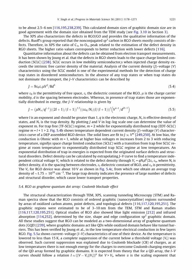
V. Singh et al. / Progress in Materials Science 56 (2011) 1178–1271 1221
to be about 2.5–6 nm [116,195,238,239]. This calculated domain sizes of graphitic domain size are ingood agreement with the domain size obtained from the TEM study (see Fig. 3.10 in Section 3).
The XPS also characterizes the defects in RGO/GO and provides the qualitative information of thedefects. Ruoff’s group reported that the nonconjugated sp3 carbon in RGO sheets mostly consists of de-fects. Therefore, in XPS the ratio of C1s to O1s peak related to the estimation of the defect density inRGO sheets. The higher ratio values corresponds to better reduction with lower defects [116].
Quantitative information about the defects can be obtained from electron transport measurements.It has been shown by Joung et al. that the defects in RGO sheets leads to the space charge limited con-duction (SCLC) [238]. SCLC occurs in low mobility semiconductor,s when injected charge density ex-ceeds the intrinsic free carrier density of the material. Analysis of the current density (J)–voltage (V)characteristics using the SCLC model is one of the experimental methods for the detection of chargetrap states in disordered semiconductors. In the absence of any trap states or when trap states donot dominate the transport, the J–V characteristics can be described by
J ¼ 9e0erlV2=8d3 ð5:4Þ
where e0 is the permittivity of free space, er the dielectric constant of the RGO, l is the charge carriermobility, d is the spacing between electrodes. Whereas, in presence of trap states those are exponen-tially distributed in energy, the J–V relationship is given by
J ¼ lNv=ql�1� �ð2lþ 1Þ=ðlþ 1Þð Þ1=l ee0=Ntð Þ l=ðlþ 1Þð Þð Þl V lþ1=d2lþ1
� �ð5:5Þ
where l is an exponent and should be greater than 1, q is the electronic charge, Nv is effective density ofstates, and Nt is the trap density. By plotting J and V in log–log scale one can determine the value ofexponent m. For trap free (TF-SCLC) regime, m = 2 while for exponentially distributed trap (EDT-SCLC)regime m = l + 1 > 2. Fig. 5.4b shows temperature dependent current density (J)–voltage (V) character-istics curve of a DEP assembled RGO device. The solid lines are fit to J1 Vm [249,250]. At low bias, theconduction is Ohmic with m = 1, while at higher bias voltages m increases from 2 to 3 with reducingtemperature, signifys space charge limited conduction (SCLC) with a transition from trap free SCLC re-gime at room temperature to exponentially distributed trap SCLC regime at low temperatures. Anexponential distribution of trap in energies is expected from the originated surface defects and struc-tural disorders. Defect density can be calculated by extrapolating J–V curve to find a temperature inde-pendent critical voltage Vc which is related to the defect density through Vc = qNtd
2/2er eo, where Nt isdefect density, d is the spacing between electrodes, er dielectric constant of RGO, and eo is permittivity.The Vc for RGO device was about 10 V as shown in Fig. 5.4c, from which one obtain an average trapdensity of �1.75 � 1016 cm�3. The large trap density indicates the presence of large number of defectsand structural disorder, which cause lower transport properties.
5.4. RGO as graphene quantum dot array: Coulomb blockade effect
The structural characterization through TEM, XPS, scanning tunneling Microscopy (STM) and Ra-man spectra show that the RGO consists of ordered graphitic (nanocrystalline) regions surroundedby areas of oxidized carbon atoms, point defects, and topological defects [116,117,120,195,251]. Thegraphitic regions were estimated to be of 3–10 nm from the TEM, STM and Raman studies[116,117,120,195,251]. Optical studies of RGO also showed blue light emission [212] and infraredabsorption [114,252], determined by the size, shape and edge configuration sp2 graphitic domain.All these studies suggest that RGO can be modeled as a two-dimensional array of graphene quantumdots (GQD) [239], where graphitic domains act like QDs while oxidized domain behave like tunnel bar-riers. This has been verified by Joung et al., in the low temperature electrical conduction in few layersRGO. Fig. 5.5a shows current–voltage (I–V) characteristics of one of their device. As the temperature islowered to less than 15 K, a complete suppression of the current below a threshold voltage (Vt) wasobserved. Such current suppression was explained due to Coulomb blockade (CB) of charges, as atlow temperatures there is not enough energy for the charges to overcome Coulomb charging energiesof the QD array formed by graphitic domains. It is expected from theory that for a QD array, the I–Vcurves should follow a relation I / ((V � Vt)/Vt))a for V > Vt, where a is the scaling exponent that

-200
-100
0
100
200
4.2 KI (pA
)
V (V)
30 K
-0.5 0.0 0.5
0.1 1
10
100
1000
10000 4.2 K
I (pA
)
(V-Vt) / Vt
15 K
5
a
b
c
Fig. 5.5. (a) Current(I)–voltage(V) characteristics of a representative RGO device at temperatures 30, 25, 20, 15, 10 and 4.2 K.Below 15 K, the current is zero for V < Vt due to coulomb blockade of charges. (b) I vs. (V � Vt)/Vt curves plotted in a log–logscale. Slope of the curves gives the value of exponent a = 3.1, 3.3, and 3.4 at 4.2 K, 10 K, and 15 K respectively. (c) Schematic ofRGO as GQD array. The light gray areas represent GQDs, the white regions represent oxidized carbon groups and topologicaldefects. The lines between GQDs represent tunnel barriers. (Reproduced with permission from [239].)
1222 V. Singh et al. / Progress in Materials Science 56 (2011) 1178–1271
depends on the dimensionality of the arrays [253]. This is also shown to be the case in RGO (Fig. 5.5b)where a was estimated to be �3.4. For a two-dimensional array of nanoparticles, the theoretical valueof a was predicted as 1.6 while numerical simulations yielded as 2.0 [253]. However, experimentalstudies of two dimensional metal nanocrystal arrays, the exponent a was reported to vary from 2to 2.5 which depends on size distribution, while for quasi 2D system with multilayered nanoparticlesthe value was 2.6–3.0 [254–258]. Therefore, the experimental results in RGO which showed a � 3.4 ishigher than 2D array system. However, recent experimental and computer simulations involve goldnanoparticles array with strong topological inhomogeneity show large scaling exponents a � 4.0[259,260]. Since RGO has a lot of topological defects which came from oxidation and reduction pro-cess, the high value of a is in agreement with charge transport in an inhomogeneous quasi 2D QD ar-ray network. Fig. 5.5c shows a schematic of RGO as a GQD array with strong topological hetrogeneity.The light gray areas represent GQDs, the white regions represent oxidized carbon groups and topolog-ical defects. This shows that the GQDs are isolated (or localized) by oxidized carbon atoms and topo-logical defects and there is strong size distribution of GQDs. The lines between GQDs indicate tunnelbarriers.
5.5. Hopping conduction in RGO
Since RGO contains a lot of disorder consisting of localized graphene domains along with oxidizedareas, the low temperature resistance measurements show hopping transport phenomenon. BothMott variable range hopping (VRH) [261,262] and Efros–shklovskii VRH [239] have been reportedin RGO.
5.5.1. Mott variable range hoppingMott described that at very low temperatures, when there is not enough thermal energy for the
charge to go from valance band to conduction band, the charge conduction occurs via hopping among

V. Singh et al. / Progress in Materials Science 56 (2011) 1178–1271 1223
the localized states [263]. When the energy is low, the carrier will hop longer distance. This is calledvariable range hopping. According to Mott, the conductivity of such a system can be described as,
Fig. 5.6with afor the[261]. (functiotherma
r ¼ A exp � T0
T1=ðdþ1Þ
� �ð5:6Þ
where A is a constant, T0 is critical temperature and d is the dimensionality of the system. So for a 2Dsystem, the relation became r � T�1/3. However, it should be noted that in Mott VRH, the Coulombinteraction among localized states is neglected and there is no minimum energy needed for the car-riers to hop. Since, RGO has a lot of defects which localizes charge carriers, it is expected that low tem-perature transport properties of the RGO can be explained using VRH model.
Kern and coworkers, first applied Mott VRH model to describe the temperature dependence of cur-rent for various back-gate voltages [261]. They showed that ln I followed linear relation with T�1/3 asshown in Fig. 5.6a. From the slope of these curves, the obtained values for T0 which in 2D is given by
T0 ¼3
NðEFÞkBL2i
!13
ð5:7Þ
where L is the localized length and N(EF) is the density of state near the Fermi level.Applying negative Vg leads to the lower value of T0 (same as B) indicate higher localization length
(Fig. 5.6b). However, the values of T0 for positive gate voltages are considerably larger than those forthe negative gate voltages, indicating shorter localization lengths (Li). Eda et al. also reported MottVRH model for their study of transport properties of RGO with various reduction process with temper-ature ranging from 78 to 300 K (Fig. 5.6c) [262]. Lightly reduced GO device (10 min and 30 min reduc-tion) showed linear trend in whole temperature ranges, while well reduced GO devices (16 h, HG-A,and HG-B) showed transition from Mott VRH (T�1/3) to Arrhenius-type (T�1) hopping above 240 K.
. (a) Natural logarithm of the measured current I vs. T�1/3 fitted to representing 2D variable range hopping in paralleltemperature-independent term, for different values of the gate voltage Vg as indicated, for bias voltages. (b) Parametersfits in figure (a), plotted as a function of gate voltage Vg for different values of bias voltage Vds (Hopping parameter B)c) Temperature and electric field dependence of the RGO device properties. Minimum conductivity rmin of RGO as an of T�1/3. The linear fits show agreement with the VRH transport. For samples 16 h, HG-A, and HG-B, deviation tolly activated transport is observed at temperatures indicated by the arrows. (Reproduced with permission from [262].)

1224 V. Singh et al. / Progress in Materials Science 56 (2011) 1178–1271
5.5.2. Efros–Shklovskii (ES) VRHEfros and Shklovskii [264–266] pointed out that for certain systems, the Coulomb energy between
localized states near the Fermi level must be overcome for a carrier to hop from one site to another. Inother words, there is a Coulomb gap near the Fermi level where the density of states vanishes. Undersuch circumstance, the conductivity is independent of dimension and should follow, ES VRH
Fig. 5.7plottedcomparFrom th
R ¼ A exp � T0
T
� �12
ð5:8Þ
where T0 is a constant related to the disorderness of the material. And the T0 is described as
T0 ¼2:8e2
4pee0kn
� �ð5:9Þ
for a 2D system, where e dielectric constant of RGO and n is localized length [264–266]. ES VRH modelwas successfully applied for granular metals and QD array systems with significant size and structuraldisorders.
Joung et al. noted that the structural information strongly suggests that RGO can be modeled as anarray of QDs with significant size and structural disorder (polydispersed QD array), which has beenverified in low temperature I–V curve [239]. In addition, recent study of individual 10 nm sized graph-ene quantum dots show room temperature Coulomb blockade (CB) [162,267]. This suggests that Cou-lomb interaction should be important in the transport study of RGO. Moreover, it was also noted thatfor a polydisperesed QD array, the temperature dependent resistance data should follow ES VRH. Thiswas experimentally verified by obtaining resistance data (calculated from the linear part of the I–Vcurve), which vary by three orders of magnitude for temperature ranges of 30–295 K. Since, fittingthe resistance data with different behavior can be tricky and the same data can often fit with severalbehaviors (such as T�1, T�1/2, and T�1/3), the behavior was determined by considering a generalizedformula R(T) = R0exp(T0/T)p and then calculating the value of p from lnW = A � p lnT, whereW = �@lnR(T)/@ lnT = p(T0/T)p is the reduced activation energy and A is a constant [268,269].Fig. 5.7a shows lnW plot vs. lnT. From the slope (indicated by red line) of this curve, p = 0.48 ± 0.05was obtained over the whole temperature range which is consistent with ES VRH. From the plot ofR verses T�1/2 in a semi-log scale (Fig. 5.7b) the value of T0 = 4200 K was calculated. The localizationlength n was calculated to be 3.5 nm which is comparable to the graphitic domain size suggestingstrong localization of wave functions inside each GQDs.
5.6. Application of RGO for photodetector, phototransistor and emitter
It is clear from different characterization and transport studies that RGO contains a lot of defectsand they do not have the same extraordinary electrical properties as pristine grapheme. However,
. Temperature dependence of the RGO device properties. (a) Reduced activation energy W = �@lnR(T)/@lnT = p(T0/T)p
vs. T on a log–log scale. From the slope of this plot we obtained p = 0.48 ± 0.05 corresponding to the ES VRH. For aison we also show lines with p = 1 (activated hopping) and p = 1/3 (Mott VRH). (b) R in log scale as a function of T�1/2.e slope, T0 = 4200 K was obtained [239].

V. Singh et al. / Progress in Materials Science 56 (2011) 1178–1271 1225
considering their high throughput processing ability, they may find many useful applications whereextraordinary electrical characteristics are not required including sensors, transparent electrodes, so-lar cells, field emitters, etc. In addition, their graphitic domain nature may also be of great use for opto-electronic applications.
Photoconductivity of bulk RGO thin film has been studied using various intensities of light, externalfield, and photon energies [270]. The study showed higher photocurrent under same photon energywith the increase of incident light intensity and external electric field. This indicates that the chargecarrier generation is influenced by the number of photons and the external field intensity in RGOsheets. Higher photoconductivity has also been observed with higher photon energy under sameintensity and electric field. The time dependent photocurrent decay results show extra time requiredto recombine charge carriers upon increase of external field and light intensity. It can be concludedthat the RGO film generates more charge carriers per unit volume upon irradiation of higher photonenergy. In comparison with SWNT, the RGO film shows high photocurrent generation efficiency [270].
Position dependent RGO thin film photo-detector has been reported by using near-infrared (wavelength of �800 nm) light [252]. Fig. 5.8a shows a schematic diagram of the device and electron trans-port measurements setup. L corresponds to illumination on the left electrode/film interface, R corre-sponds to illumination on the right electrode/film interface, and M corresponds to the middle positionof the film. Fig. 5.8b shows the photocurrent with different laser spot positions. The photocurrenteither increases and decreases or remains almost zero depending on the position of the laser spot withrespect to the electrodes. In detail, the I–V curves for position M and in dark lie on top of the one an-other and pass directly through the origin. Whereas, when the light illuminated at position L and R, theI–V curve is shifted above or below the origin respectively. A large enhancement of photocurrent aswell as a finite photo-voltage at the interface indicates that there is an existence of locally generatedelectric field at the metal-RGO film interface. This mechanism of the local electric field generation wasexplained using Schottky barrier (SB) model. In schematic diagram (Fig. 5.8c), the black filled and opencircles inside the dotted oval region represent the photogenerated excitons (bound electron–hole pair)due to absorption of NIR source (curved red arrow). Solid line is the potential variation within thegraphene channel and dashed lines are the Fermi levels (EF) of the two electrodes. When NIR is illu-minated on the left electrode/RGO film interface, excitons are generated and dissociated into freecharge carriers at the interface. Since RGO thin film has a lot of defects, it will also help in dissociationof excitons into free carriers. Some of the free carriers (holes) might have sufficient energy to over-come the SB and enter into the metal electrode leaving the electron in the film. This causes a hole–electron separation at the interface creating a positive photo-voltage. In addition, the time constantof the dynamic photo response was �2.5 s which is much larger compared to the single sheets of pris-tine graphene, possibly due to the disorder from the chemical synthesis and interconnection of sheets.
RGO FET phototransistor also has been studied based on their energy band gap values [271]. In thiscase, RGO FET, in which few layer RGO sheets serves as the semiconducting channel and is designed toconduct positive and negative charge carriers (holes and electrons, respectively). The band gap, which
Fig. 5.8. (a) Schematic diagram of the device and electron transport measurement setup. L, M, and R are three differentpositions of NIR illumination. (b) Current–voltage characteristics of the device at three different illumination positions. (L, R,and M) and under dark condition. (c) A cartoon for photo-voltage generation at the metallic electrode/RGO interface.(Reproduced with permission from [252].)

1226 V. Singh et al. / Progress in Materials Science 56 (2011) 1178–1271
ranges from 2.2 eV to 0.5 eV, can be made tunable by reduction treatments. These results also indicatethat the photosensitivity is strongly related to the number of oxidized functional group. The roughestimation of the photosensitivity of RGO FET was calculated to be around 0.85 A W, three orders low-er than that of the pristine graphene [272].
In addition to RGO thin film, the optical properties of individual GO/RGO sheet was also studied.Semiconducting GO/RGO shows absorption from ultraviolet (UV) to infrared (IR), wavelength of from10 to 2500 nm [97,114,209,212,273]. Acik et al. reported that the single layer GO and RGO have dif-ferent response of infrared absorption band due to their different functional groups on the edge region(Fig. 5.9a and b) [114]. If the GO is well reduced, oxygen-containing functionalized groups get re-moved and the infrared spectra of RGO become strong due to the in-phase electron band populationwith mobile electrons localized at the edge resulting in stronger absorption. In another study, Edaet al. [212] demonstrated that RGO thin films emitted near-UV blue light, when excited with UV radi-ation. The blue photoluminescence (PL) was observed for the RGO sheets. By appropriately controllingthe reduction process, the PL intensity increased by a factor of 10 compared to the as-synthesized GOsheets. The results indicated that RGO offers tunable optoelectronic device via controlling the reduc-tion process through chemical and/or thermal route.
5.7. Graphene thin film as transparent electrodes
It has been demonstrated that thin film (<30 nm) of RGO is semi-transparent to visible and NIR re-gion while thick films are opaque. The transmittance and conductivity of the GO/RGO film can betuned by tuning the thickness of the film and the degree of reduction [28]. Fig. 5.10 shows how thetransparency of RGO varies with film thickness. The leftmost film is 9 nm thick GO while rest of thefilms are RGO (annealed in 1100 �C for 3 h) with thickness 6, 8, 27 and 41 nm (from left to right).As it can be seen that, as the film gets thicker, the transmittance gets reduced. While the conductivityof the RGO thin film increases with the degree of reduction and transmittance decrease. Therefore, theoptimization of film thickness and reduction parameters is the key in achieving high performancetransparent and conducting RGO thin film. Table 5.1 summarizes the recent progress on optoelec-tronic properties of graphene-based thin films in terms of their reduction and fabrication methods.
Optical and mechanical properties of RGO thin film were also studied on flexible substrates. Forexample, Yin et al. [278] studied the effect bending on the properties of RGO for film thickness of4–21 nm. After applying tensile stress (tensile strain of 2.9%) on the device, the performance was mon-itored by resistance change with the number of bending cycles. The device showed an excellence sta-bility of resistance, even when bending cycles reached about 1000 times.
Fig. 5.9. (a) Transmission infrared-absorbance spectrum of GO-1L. (b) Transmission infrared absorption spectra of thermallyreduced GO-1L after annealing at 850 �C. (Reproduced with permission from [114].)

Table 5.1Progress in graphene-based transparent electrodes and their properties.
Materials Reduction Fabricationmethod
Filmthickness
Sheetresistanc(X/square)
Wavelength(nm)
Transmittance(%)
References
RGO Hydrazinesolution/annealing
Spray coating �1 nm 20 M 600–1000 96 [194]
RGO Hydrazine vapor/annealing
Vacuumfiltration
�3 nm 0.16 M 550 90 [197]
RGO Hydrazine vapor LB 1–3 nm 8 K 1000 83 [36]RGO Hydrazine vapor/
annealingSpin coating 1 102–103 400–1800 80 [28]
RGO Acetylene-assistedthermal
Spin coating 1.1 1425 500 70 [274]
RGO SOCl2 treatment Vacuumfiltration
�10 nm 40 K 300–900 64 [230]
RGO/SWNT Hydrazinesolution/annealing
Spin coating 5 nm 240 UV visible 86 [275]
RGO Hydrazinesolution/annealing
Spin coating 5–8 0.4–19 K 1000 60–80 [276]
RGO (OLEDdevice)
Vacuumannealing
Spin coating �7 0.8 K 550 82 [277]
Fig. 5.10. Optical and electrical characterization of spin coated GO films on quartz. (A) Photograph of an unreduced (leftmost)and a series of high-temperature reduced GO films of increasing thickness. Black scale bar is 1 cm. (B) Optical transmittancespectra of the films in (A) with the film thickness indicated. (Reproduced with permission from [28].)
V. Singh et al. / Progress in Materials Science 56 (2011) 1178–1271 1227
Due to their transparency, conducting and flexible nature, RGO thin film is considered to be apromising electrode material for organic electronic and optoelectronic applications. Presently, indiumdoped tin oxide (ITO) is widely used as transparent and conducting electrodes in optoelectronic appli-cation. However, the ITO based materials are expensive [279] and their limitation of mechanical flex-ibilities [280] makes them un-attractive for flexible display and solar cell applications. In this respect,RGO electrodes provide several advantages; (i) possibilities on one phase reaction without additionalsurfactant due to water soluble properties, (ii) the homogeneity and composition of the films are sim-ply determined by the composition of the parent suspension and surface modification of the substrate,(iii) relatively inexpensive starting materials, and (iv) low temperature and high throughput process-ing. In addition, the work function of RGO (4.2–4.6 eV) matches with the HOMO level of most of theorganic materials, and p–p interaction exists between RGO and organic material [276,278].
Several research groups successfully used RGO electrode for the fabrication of organic light emit-ting diodes (OLED) and solar cells. Efficient RGO-based OLEDs have been first demonstrated by Wu

1228 V. Singh et al. / Progress in Materials Science 56 (2011) 1178–1271
et al. [277]. The RGO-based OLED performance nearly matches with that of the ITO based device, eventhough higher resistance (800X/square) and different work function of the RGO anodes. Wang et al.reported that RGO films can be employed for fabrication of dye-sensitized solar cells [224]. In thisapplication, Spiro-OMeTAD was used as a hole transport material, and porous TiO2 used for electrontransport materials. The solar cell was fabricated using RGO as an anode and Au as cathode (Fig. 5.11a).Fig. 5.11b shows the energy level diagram of a RGO (4.42 eV)/TiO2/dye/spiro-OMeTAD/Au (5.0 eV) de-vice. The electrons are first injected from the excited state of the dye into the lowest unoccupiedmolecular orbital (LUMO) level of TiO2 and then reached the RGO electrode via a percolation mecha-nism inside the porous TiO2 structure. Meanwhile, the photo-oxidized dyes are regenerated by thespiro-OMeTAD hole conducting molecules (highest occupied molecular orbital (HOMO)) and then holeinjecte into Au cathode. Fig. 5.11c shows I–V curve of the solar cell using RGO (black curve) as anodeand the comparison with fluorine tin oxide (FTO) (red curve) electrode. Lower short-circuit current inRGO electrode lead to low power conversion efficiency (0.26%) compared to FTO (0.84%). This may bedue to the series of resistance of the device, lower transmittance of the materials (70.7%), and spacecharge limited conduction on contact between active materials and RGO electrodes.
To overcome the contact problem, Yin et al. [276] suggested the use of hole transport interlayer(ZnO nanorod) between RGO electrodes and active polymeric materials by electrochemical deposition.The structures of the device was RGO/ZnO/P3HT/PEDOT:PSS/Au. The observed higher power conver-sion efficiency of 0.31% was demonstrated, compared to ZnO-free interlayer. As can be seen, the solarcell fabricated with RGO electrode suffers from low efficiency and more work is needed to make RGOas an efficient electrode material.
5.8. Solar cell using GO/RGO
As mentioned in the previous section, RGO transparent electrodes can be used for solar cell elec-trode. Several studies suggest that GO/RGO can also be used as hole transport layer as well as a partof active material. In vertical bulk heterojuntion (BHJ) devices, both the donor and acceptor phases arein the direct electrical contact with the cathode and anode electrodes. Most vertical organic solar cellsare composed of ITO/P3HT:PCBM/Al configuration. The polymeric donor and acceptor materials oftenresults in recombination of carriers and current leakage. To minimize such detrimental effects, elec-tron blocking and hole transport layers (HTLs) are deposited on top of the transparent and conductingITO anode (Fig. 5.12a) [281]. The most common HTL in polymer solar cells is PEDOT:PSS. However,PEDOT: PSS combination has been made from highly acidic aqueous suspensions that corrodes theITO at high temperatures and contributes water/moisture into the active layer, which leads poor de-vice performance [281]. To overcome this issue, ITO/GO/P3HT:PCBM/Al configuration was introducedfor more efficient collection of holes and the band energies of the configuration are 4.4–4.5/4.9/4.9:4.2/4.2 eV respectively. Interestingly the power efficiency values are dependent on GO film thin-ness. GO thickness of 2 nm has shown best efficiency performance compared to higher thickness(>4 nm) due to the increase in serial resistance and the slightly lower transmittance of the films withthickness.
Fig. 5.11. (A) Illustration of dye-sensitized solar cell using graphene film as electrode, the four layers from bottom to top are Au,dye-sensitized heterojunction, compact TiO2, and graphene film. (B) The energy level diagram of graphene/TiO2/dye/spiro-OMeTAD/Au device. (C) I–V curve of graphene-based cell (black) and the FTO-based cell (red), illuminated under AM solar light(1 sun). (Reproduced with permission from [224].)

Fig. 5.12. (a) Schematic of the photovoltaic device structure consisting of the following: ITO/GO/P3HT:PCBM/Al. (b) Energylevel diagrams of the bottom electrode ITO, interlayer materials (PEDOT:PSS, GO), P3HT (donor), and PCBM (acceptor), and thetop electrode Al (Reproduced with permission from [281].) (c) The schematic chemical structure of SPF Graphene and P3HT. (d)Schematic structure of the devices with the P3HT/SPF graphene thin film as the active layer; ITO (�17 X sq�1)/PEDOT:PSS(40 nm)/P3HT:SPFGraphene (100 nm)/LiF (1 nm)/Al (70 nm). (Reproduced with permission from [282].)
V. Singh et al. / Progress in Materials Science 56 (2011) 1178–1271 1229
Other studies have shown the use of RGO as acceptor materials in the BHJ photovoltaic devices. Forinstance, Liu et al. reported the organic solution-processable RGO as an acceptor material in organicphotovoltaic devices with P3HT as an electron-donor materials [282]. Fig. 5.12b shows a schematicdiagram of a solar cell using RGO as an active material. The RGO was well dispersed in P3HT with10 wt% doping. The properties of the materials induce quenching of the photoluminescence (PL) ofthe P3HT and lead to strong electron/energy transfer from the P3HT to the RGO. Power-conversionefficiency �1.1% was achieved by using RGO as an active material. Table 5.2 shows the role of graph-ene-based materials in solar cell and their photovoltaic properties including RGO as an active materi-als as well as an electrode.
Table 5.2GO/RGO in solar cell and their photovoltaic properties.
Activematerial
Electrodematerial
Reduction Deposition Thickness(nm)
Fillfactor(FF)
Power-conversionefficiency(%)
Role ofGO/RGO
References
P3HT:PCBM RGO/PET Thermal Spincoating
16 0.32 0.78 Electrode [278]
TiO2 film(RGO/TiO2
compositeinterlayer)
FTO Photocatalyticallyby UV irradiation
Spincoating
�15 N/A 5.26 Interfaciallayer
[283,284]
P3HT:graphene/PEDOT:PSS
Al:LiF/ITO
Thermal Spincoating
100 withP3HT
0.3 1.1 Acceptor [285]
PEDOT:PSS/P3HT/ZnO nanorods
Au/RGO Hydrazine vapor/thermal
Spincoating
5–13 0.33 0.31 Electrode [276]
TiO2/dye/spiro-OMeTAD
Au/RGO Thermal Dipcoating
10 0.36 0.84 Electrode [224]

1230 V. Singh et al. / Progress in Materials Science 56 (2011) 1178–1271
5.9. Electrochemical sensors and biosensors
RGO is highly promising for electrochemical and biological sensors due to their different function-alities on the edge [286–288] which are very sensitive to change in chemical and biological environ-ment. The responses have been analyzed by changes in conductivities, capacitances, and dopingeffects on FETs made with RGO. Table 5.3 summarizes the sensors fabricated with RGO based-materials.
Table 5.3Graphene based chemical/biosensors.
Activematerial
Reductionmethod
Sensor type Analyte Measurement Detectionlimits
References
RGO Thermal Gas NO2, NH3 I vs. t �100 ppm [289]RGO + Pd Chemical Gas H2 R vs. t N/A [290]RGO Thermal Molecular HCN, CEES DMMP,
DDTG vs. t �ppb [226]
RGO Chemical Gas NO2, NH3, DNT R vs. T �ppm [287]RGO Chemical Electrochemical/
chemicalElectroactive compound(potassium ferricyanide,free bases of DNA),neurotransmitter(dopamine),biological molecule(ascorbic acid, uricacid, acetaminophen)
I vs. E/V �lM [291]
RGO + DNA Chemical Bio DNA, bacterium G �single-strandedDNA,molecule�singlebacterium
[99]
RGO + Au Electrochemical Bio DNA I vs. E/V �lM/L [292]SDBS
functionalizedgraphene(RGO + HRPa)
Chemical Bio H2O2 I vs. t �30 lM [293]
RGO + Auantibody
Thermal Bio R vs. t �ng/ml [294]
GO N/A Bio DNA, Protein Fluorescenceintensitychange
�nM [295]
GO/MNO2 N/A Bio H2O2 I vs. E/V andI vs. t
�lM [296]
RGO Thermal Gas NO2 I vs. t �ppm [297]RGO Thermal,
chemicalGas Water vapor R vs. t N/A [241]
RGO, RGO/Nafion,Fatigued-RGON
Chemical Bio Organo Phosphate(OPH)
I vs. E/Vand I vs. t
1.39 lM,0.137 lM,0.360 lM
[298]
RGO (inkjetprinter)
Chemical Gas (Vapor) NO2, Cl2 R vs. t �ppm [299]
RGO Chemical Molecule(Redox species)
Ru(NH3)63+/2+, Fe
(CN)63�/4�, Fe3+/2+
I vs. E/V �mM [300]
GO-CdTe(NPs or QDs)
N/A Molecule Thiole-containingcompound
I vs. E/V �lM [301]
Pt/RGO/SiC Thermal Gas H2 I vs. t N/A [302]
a HRP: Horseradish peroxide a type of enzyme, current (I), conductivity (G), resistance (R), potential E/V, time (t), ppm: partper million, ppb: part per billion, SDBS: sodium dodecyl benzene sulphonate.

V. Singh et al. / Progress in Materials Science 56 (2011) 1178–1271 1231
The sensitivity of the gas (or vapor phase) sensor depends on the charge carrier transfer on GO/RGOsurfaces caused by the adsorption of gases and vapors such as NO2, NH3, H2O, CO, dinitrotoluene(DNT), Iodine, and ethanol and hydrazine hydrate [226,286–288,303,304]. For example, the as-synthesized GO transistor showed little response to chemical gases such as NO2 [287]. In contrast,the RGO was highly responsive to NO2 and showed a typical p-type transistor behavior most likelydue to the recovery of many graphitic carbon atoms as active sites for NO2 adsorption, which leadsto enhancing charge concentration. This leads to a decrease in resistance as a function of time(Fig. 5.13a). The NH3 makes n-type RGO transistor behaviors [289,297] since oxygen groups in RGOwere responsible for reactions with NH3 and CAN bond [243]. This reaction decreases device conduc-tivity (Fig. 5.13b) as a function of time [287].
High temperature (�1000 �C) reduced GO shows faster chemoresistive (or resistance changes intime) response than the hydrazine and low temperature reduction upon exposure to water vapor. Thisis attributed to the presence of larger number of defects during the high temperature reduction pro-cess [241]. These results indicate that the gaseous vapor may respond with both structural defects,such as vacancies and/or small holes generated during reduction treatments, and functionalizedgroups. Therefore, the sensitivity of RGO based sensors can be modified by controlling of reductiontreatment process [226,241].
Besides chemical (by hydrazine) and thermal reduction, the ascorbic acid (vitamin C) has also beenused as a mild and green reduction agent for RGO based chemical sensors [299]. The flexible RGOchemical sensor, using inkjet-printed films of poly-(ethylene terephthalate) (PET) decorated RGOsheets reversibly detect NO2 and Cl2 vapors at parts per billion level. This demonstrates the use ofascorbic acid as an effective alternative to hydrazine to reduce GO into RGO.
Graphene based composite materials have been studied for gas sensor. For example, Pt/RGO/SiCbased devices for hydrogen gas sensing [302]. The electrical characteristics and hydrogen gas sensingmechanism of the device were described by analyzing the effect of hydrogen interaction at the graph-ene/SiC and Pt/graphene interfaces. High work function of Pt leads to a weak interaction energy at theinterface and preserves the electronic structure of RGO and electrons transfer from RGO to Pt to equil-ibrate the Fermi level. Upon exposure of hydrogen gas, the carrier concentration is increased due todissociation of hydrogen molecules, which occurs on the Pt surface.
Several studies have been demonstrated RGO based biosensors as well. Mohanty and Berry [99]reported on the fabrication and functioning of a novel RGO-based (i) single-bacterium device, (ii)label-free DNA sensor, and (iii) bacterial DNA/protein and polyelectrolyte transistor. The bacteria/RGO bio-device was highly sensitive with a single bacterium with a p-type FET property. The presenceof DNA on RGO increased both the conductivity and the mobility (Fig. 5.14 a and b) due to the inter-action between the charged amine group and the RGO. Similarly, single-stranded DNA when tetheredon graphene, hybridizes with its complementary DNA strand which reversibly increases the hole den-sity by 5.61 � 1012 cm�2. Also the bending-insensitive RGO FETs were able to detect the presence and
Fig. 5.13. (a) NO2 detection and (b) NH3 detection using a graphene film. The sensor has gold electrodes and measurement useda four wire method with 500 lA driving current. The NO2 concentration is 5 ppm in dry nitrogen. (Reproduced with permissionfrom [287].)
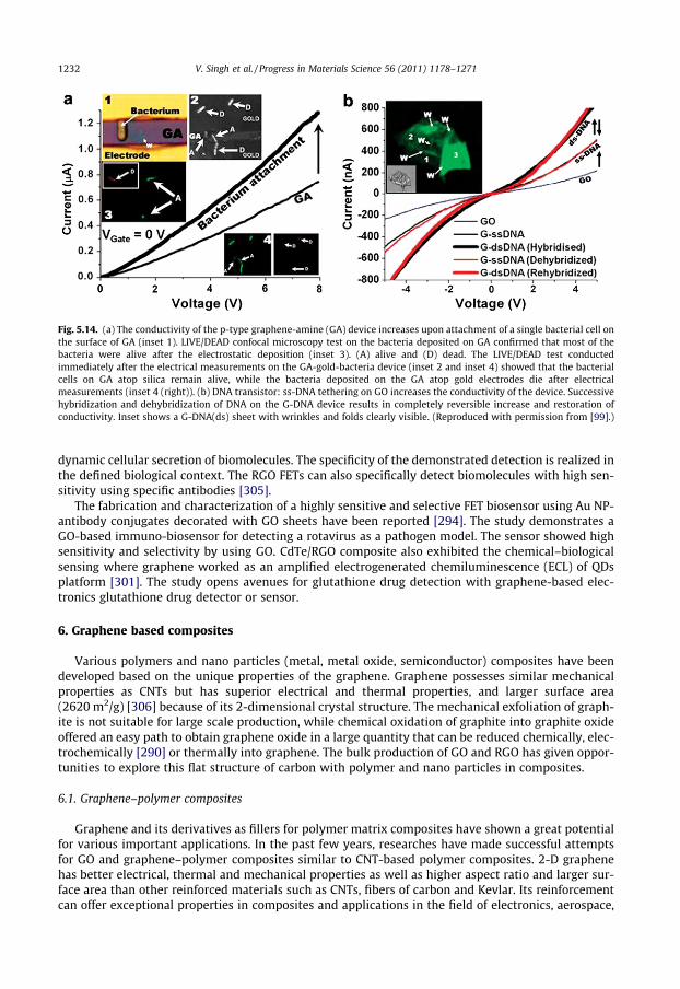
Fig. 5.14. (a) The conductivity of the p-type graphene-amine (GA) device increases upon attachment of a single bacterial cell onthe surface of GA (inset 1). LIVE/DEAD confocal microscopy test on the bacteria deposited on GA confirmed that most of thebacteria were alive after the electrostatic deposition (inset 3). (A) alive and (D) dead. The LIVE/DEAD test conductedimmediately after the electrical measurements on the GA-gold-bacteria device (inset 2 and inset 4) showed that the bacterialcells on GA atop silica remain alive, while the bacteria deposited on the GA atop gold electrodes die after electricalmeasurements (inset 4 (right)). (b) DNA transistor: ss-DNA tethering on GO increases the conductivity of the device. Successivehybridization and dehybridization of DNA on the G-DNA device results in completely reversible increase and restoration ofconductivity. Inset shows a G-DNA(ds) sheet with wrinkles and folds clearly visible. (Reproduced with permission from [99].)
1232 V. Singh et al. / Progress in Materials Science 56 (2011) 1178–1271
dynamic cellular secretion of biomolecules. The specificity of the demonstrated detection is realized inthe defined biological context. The RGO FETs can also specifically detect biomolecules with high sen-sitivity using specific antibodies [305].
The fabrication and characterization of a highly sensitive and selective FET biosensor using Au NP-antibody conjugates decorated with GO sheets have been reported [294]. The study demonstrates aGO-based immuno-biosensor for detecting a rotavirus as a pathogen model. The sensor showed highsensitivity and selectivity by using GO. CdTe/RGO composite also exhibited the chemical–biologicalsensing where graphene worked as an amplified electrogenerated chemiluminescence (ECL) of QDsplatform [301]. The study opens avenues for glutathione drug detection with graphene-based elec-tronics glutathione drug detector or sensor.
6. Graphene based composites
Various polymers and nano particles (metal, metal oxide, semiconductor) composites have beendeveloped based on the unique properties of the graphene. Graphene possesses similar mechanicalproperties as CNTs but has superior electrical and thermal properties, and larger surface area(2620 m2/g) [306] because of its 2-dimensional crystal structure. The mechanical exfoliation of graph-ite is not suitable for large scale production, while chemical oxidation of graphite into graphite oxideoffered an easy path to obtain graphene oxide in a large quantity that can be reduced chemically, elec-trochemically [290] or thermally into graphene. The bulk production of GO and RGO has given oppor-tunities to explore this flat structure of carbon with polymer and nano particles in composites.
6.1. Graphene–polymer composites
Graphene and its derivatives as fillers for polymer matrix composites have shown a great potentialfor various important applications. In the past few years, researches have made successful attemptsfor GO and graphene–polymer composites similar to CNT-based polymer composites. 2-D graphenehas better electrical, thermal and mechanical properties as well as higher aspect ratio and larger sur-face area than other reinforced materials such as CNTs, fibers of carbon and Kevlar. Its reinforcementcan offer exceptional properties in composites and applications in the field of electronics, aerospace,

V. Singh et al. / Progress in Materials Science 56 (2011) 1178–1271 1233
automotive and green energy. The recent advancement in bulk synthesis processes of graphene andRGO has generated great interest to incorporate such unique material into various polymer matrices.Several challenges need to be overcome to realize graphene or graphene oxide based polymercomposites,
1. Functionalization of graphene sheets2. Homogeneous dispersion of materials with minimal restacking3. Effective mixing of graphene oxide and graphene with polymer4. Understanding of the interfacial structure and properties5. Controlling the folding, crumpling and bending of graphene materials
This section is devoted to only graphene and graphene oxide–polymer composites and highlightstheir properties and applications.
Two potential approaches are commonly used to produce a single layer of graphene with highyield: (1) chemical and (2) thermal reduction of exfoliated sheets of graphene oxide, as explainedin earlier sections. Both the methods disrupt the conjugated electrical structure of graphene and re-duce the electrical conductivity. On the other hand, the functional groups introduced by these invasiveapproaches can be used to achieve good dispersion of derived graphene in different solvents. Numer-ous efforts have been made to improve the dispersion of GO and RGO by functionalizing the use oforganic molecules compatible with the polymer matrix to enhance interfacial interaction with matrix.For example, GO has carboxylic, hydroxyl and epoxy groups on the surface which improve its disper-sion in water and keep individual layers separated from each other [26,307]. However, these func-tional groups and defects on GO make it electrically insulating and thermally unstable, and theremoval of these functional groups during reduction makes RGO hydrophobic and increases tendencyto agglomerate irreversibly in an aqueous medium unless stabilized by polymers and surfactants [82].The dispersion behavior of GO in different organic solvents has been demonstrated in Fig. 6.1, whichcan guide the selection of compatible polymer matrix for bulk synthesis [75].
The dispersion of graphene oxide and reduced graphene against their agglomeration in organic sol-vents, after complete exfoliation of graphitic layers, has been achieved by surface functionalizationthrough non-covalent and covalent bonding [75,308,309]. Various organic functional groups such aspolystyrene [69,308], 1-pyrenebutyrate [310], dopamine [311], 7,7,8,8-tetracyanoquinodimethane[312], coronene carboxylate [313] have been used to produce stable aqueous and organic solvent dis-persion and facilitated nanocomposite synthesis to induce desirable properties.
Non-covalent functional groups including 1-pyrenebutyrate [310] and 7,7,8,8-tetracyanoquinodi-methane [312] have strong affinity with the basal plane of graphite through p–p interactions, whilecovalent functional groups attach to the surface through the reaction between the functional groups(AOH, ACOOH, ACO) present on the GO and RGO surfaces and edges. For example, Xu et al. have dem-onstrated the covalently functionalized GO through the coupling amine-functionalized prophyrin(TPP-NH2) and carboxylate groups [93]. The covalent polymer functionalization of graphene
Fig. 6.1. Digital pictures of as-prepared graphite oxide dispersed in water and 13 organic solvents through bath ultrasonication(1 h). Top: dispersions immediately after sonication. Bottom: dispersions 3 weeks after sonication. The yellow color of the o-xylene sample is due to the solvent itself. (Reproduced with permission from [75].)

1234 V. Singh et al. / Progress in Materials Science 56 (2011) 1178–1271
nanosheets via atom transfer radical polymerization (ATRP) initiator was recently reported[100,101,314] to achieve the dispersion of graphene sheets in polymer matrix and precise interfacecontrol (Fig. 6.2). The ATRP initiator covalently immobilized on the surface of the graphene was sub-sequently used for grafting polymer brushes from the sheets surface. Such controlled polymerizationallows the control of the molecular structure of the grafted polymer, providing an effective approachto tune the properties of the hybrids.
In this approach, the initiator molecules were covalently attached to the graphene surfaces via dia-zonium addition. The subsequent atom transfer radical polymerization linked ATRP compatible poly-mer chains (i.e. polystyrene, polymethyl methacrylate) to the graphene sheets. Another example ofthe covalent functionalization of graphene sheets with polymers is through grafting-to process bythe esterification of carboxylic groups in GO. The covalent functionalization of sheets with polyvinylalcohol (PVA) via the esterification provided a facile way of producing water and DMSO soluble, sim-ilar to PVA [315].
6.1.1. Synthesis of graphene reinforced polymer compositeThe method of solution blending, melt mixing, and in situ polymerization are the most common
synthesis strategies of the polymer matrix composites. These methods will be summarized in thissection.
6.1.1.1. Solution blending. Solution blending is the most common technique to fabricate polymer-basedcomposites provided the polymer is readily soluble in common aqueous and organic solvents, such aswater, acetone, DMF, chloroform, DCM and toluene. This technique involves the solubilization of thepolymer in suitable solvents and mixing with the solution of the dispersed graphene suspension. Thepolar polymers including PMMA, PAA, PAN and polyesters have been successfully mixed with GO insolution blending where the GO surface was usually functionalized by isocyanates, alkylamine, alkyl-chlorosilanes, etc., to improve its dispensability in organic solvents. For instance, esterificated GO wasmixed with PVA dissolved in DMSO to fabricate the PVA–GO nano composite [315].
To homogenize the dispersion of graphene sheets, ultrasonic power can be used to produce meta-stable suspension. It is important to note that long time exposure to high power ultrasonication caninduce defects in graphene sheets which are detrimental to the composite properties. Functionaliza-tion of graphene sheets may help in obtaining a higher loading of sheets and allow dispersion in waterand other organic solvents. During the blending, the polymer coats the surface of the individual sheetand interconnects each sheet after the solvents are removed. Solution blending of GO and RGO sheetstend to agglomerate during slow solvent evaporation, resulting in inhomogeneous distribution ofsheets in polymer matrix. The distribution can be controlled by controlling the evaporation time usingspin coating or drop casting. Various polymer composites such as graphene–PVA [316], GO–PVA [317],
Fig. 6.2. Synthesis route of polystyrene functionalized graphene nanosheets. (Reproduced with permission from [101].)

V. Singh et al. / Progress in Materials Science 56 (2011) 1178–1271 1235
graphene–PVC [318], PVA–GO layer by layer assembly [319], and PVDF-thermally reduced graphene[320] have been prepared using this technique.
6.1.1.2. Melt mixing. Melt mixing technique uses a high temperature and shear forces to disperse thereinforcement phase in the polymer matrix. The process avoids the use of toxic solvents. The hightemperature liquefies the polymer phase and allows easy dispersion or intercalation of GO and re-duced graphene sheets. The melt mixing is less effective in dispersing graphene sheets compared tosolvent blending due to the higher viscosity of the composite at increased sheets loading. The processcan be applicable to both polar and non-polar polymers. However, this technique is more practical forthermo plastic manufacturing composite in large scale. Varieties of graphene reinforced compositessuch as, exfoliated graphite–PMMA [321], graphene–polypropylene (PP), GO-poly (ethylene-2,6-naphthalate) (PEN) [322] and graphene–polycarbonate [323], are prepared by this method. Lowthroughput of chemically reduced graphene restricts the use of graphene in the melt mixing process.However, graphene production in bulk quantity in thermal reduction can be an appropriate choice forindustrial scale production. The loss of the functional group in thermal reduction may be a hurdle inobtaining homogeneous dispersion in polymeric matrix melts especially in non-polar polymers. Kimand Macosko [323] have not observed significant improvement in mechanical properties due to theelimination of the oxygen functional groups, which affected the interfacial bonding in graphenecomposite with polycarbonate and PEN, and the defects caused by high temperature reduction.
6.1.1.3. In situ polymerization. This fabrication technique starts with the dispersion of GO or RGO inmonomer followed by the polymerization of the monomers. Like solution blending, functionalizedgraphene and GO sheets can improve the initial dispersion in the monomer liquid and subsequentlyin the composites. The in situ polymerization technique enables the covalent bonding between func-tionalized sheets and polymer matrix through various condensation reactions. On the other hand,non-covalent bonded composites such as PMMA–GO [324], PP–GO [325] and PE-graphite [326] havealso been prepared by this technique. Extensive research has been performed on producing epoxy-based nano composites using in situ polymerization where sheets are first dispersed into resin fol-lowed by curing by adding hardener [284]. Recently, graphene oxide sheets have been used for Mg/Ti catalysis support for in situ Ziegler–Natta polymerization of PP, process are shown in Fig. 6.3 [325].
The prepared composite showed a good exfoliation of GO and homogeneous dispersion in PP ma-trix (Fig. 6.4), leading to high electrical conductivity. In situ polymerization has also been explored
Fig. 6.3. Fabrication of PP/GO nanocomposites by in situ Ziegler–Natta polymerization. (Reproduced with permission from[325].)

1236 V. Singh et al. / Progress in Materials Science 56 (2011) 1178–1271
widely for the high level of dispersion of graphite-based layered structure in a polymer matrix, such asexpanded graphite and graphite oxide [326–328]. The in situ polymerization increases interlayer spac-ing and exfoliates the layered structure of graphite into graphite nano plates by the intercalation ofmonomers that generate polymers after polymerization, producing well-dispersed graphene in a poly-mer matrix. This approach has produced a variety of composites, such as PANI–GO/PANI–graphene[329], graphene nanosheet/carbon nanotube/polyaniline [330], and PANI–GO [331].
6.1.2. Mechanical propertiesHigher mechanical properties (elastic modulus and tensile strength) of graphene sheets have at-
tracted the attention of researchers. The polymer reinforced with graphene has been employed toexplore intrinsic strength (125 GPa) and elastic modulus (1.1 TPa) of nanosheets to bulk polymercomposites. Similar to other composites, the mechanical properties are dependent on the reinforce-ment phase concentration and distribution in the host matrix, interface bonding, and reinforcementphase aspect ratio, etc. For example, an increase in tensile strength of the composite (graphene–PS)with reinforcement concentration is shown in Fig. 6.5, representing an increase in the mechanicalproperties of the composite attributed to effective load transfer between graphene and polymer[101].
Fig. 6.4. (A) PP/GO nanocomposites powder as obtained after coagulation in ethanol (containing 0.1 M HCl). (B) SEM imagesobtained from fracture surface of neat PP without GO. (C–E) SEM images obtained from fracture surface of composite samples of0.42, 1.52, and 4.90 wt%, respectively, GO loadings. (F) TEM image of sample PP1 with 0.96 wt% of GO (the inset showing themeasured electron diffraction pattern). (G) TEM image of sample PP3 with 1.52 wt% of GO. (H) TEM image of sample PP4 with4.90 wt% of GO. (Reproduced with permission from [325].)

Fig. 6.5. (a) Representative stress-strain curves of the pristine PS and nanocomposite films with different contents of graphenesheets. (b) Young’s modulus and tensile strength changes with increasing graphene content. (Reproduced with permission from[101].)
V. Singh et al. / Progress in Materials Science 56 (2011) 1178–1271 1237
Although the pristine graphene has the highest theoretical strength, the presence of functionalgroups on the GO surfaces has the additional benefits of its high level of dispersion in polar solventsand water. The improved GO/polymer interaction facilitates high molecular level dispersion and en-hanced interfacial interaction, leading to high mechanical properties. For example, GO–PVA compositeshowed enhancement in mechanical properties by 76% and 62% in elastic modulus and strength,respectively, with 0.7 wt% GO sheets [317]. Xu et al. have also observed a similar trend for GO–PVAcomposite films with a layered structure prepared by vacuum filtration [332]. Whereas, situation withthe chemically reduced graphene oxide (CRG) and thermally reduced graphene oxide (TRG) is differ-ent, the presence of defects arise in carbon lattice due to the reduction process certainly have an ad-verse effect on the mechanical properties [120,317,322]. High surface defects and wrinkles in TRGreinforced in poly (ethylene-2,6-naphthalate) (PEN) indicated a relatively small increase in tensileproperties compared to the graphite reinforced PEN.
The interaction of graphene and polymer at the interface of effective load transfer has been exten-sively investigated. The tailoring of mechanical properties by a covalent and non-covalent bond con-figuration between the matrix and sheets reinforcement can provide exceptional features. Theresponsible Van der Waals forces and hydrogen-bond interactions were reported for improvedmechanical properties [316,333]. A recent ATRP strategy has been shown to grow styrene, methylmethacrylate, or butyl acrylate polymer brushes directly from the GO surfaces without damagingthe GO structure [102]. One study used a similar strategy and revealed that when pre modified GOwith PMMA chain synthesized via ATRP and mixed with PMMA matrix have better dispersion andinterfacial bonding. The results showed that the loading of 1% (w/w) GO grafted PMMA made tougherfilms than the pure PMMA films and unmodified GO–PMMA films. The elastic modulus and tensilestrength values were slightly lower than that of the pure PMMA films [314].
Research in graphene-based composites has been concentrated on improving the stiffness and themechanical strength using graphene as filler [317,334–337]. Other mechanical properties, fracturetoughness, fatigue, and impact strength of the graphene reinforced composites were also studied[284,338–340]. Recent, investigation about graphene reinforced Nayon-12, has shown the significantimprovement with 0.6 wt% addition of graphene filler in tensile strength and elongation at break by35% and 200% respectively. While, the improvement in KIc and impact failure energy were by 72%and 175% respectively. It has also shown that the graphene filler suppressed the crack propagationin epoxy polymer matrix. The improvement in fracture and fatigue resistance was similar to CNTand nanoparticles reinforcement but only need one to two orders of magnitude lower weight fractionof graphene nanofiller to achieve the same degree of reinforcement [284]. The superior mechanicalproperties of composite made of graphene platelets over carbon nanotubes was related to their highspecific surface area, enhanced nanofiller matrix adhesion/interlocking arising from their wrinkled(rough) surface and 2-D flat geometry [340].

1238 V. Singh et al. / Progress in Materials Science 56 (2011) 1178–1271
6.1.3. Electrical propertiesThe most fascinating property of graphene is its very high electrical conductivity. When used as fill-
ers with insulating polymer matrix, conductive graphene may greatly enhance the electrical conduc-tivity of the composites. Various factors have been corroborated by experimental results that influencethe electrical conductivity and the percolation threshold of the composite. These factors include theaggregation of filler, the presence of functional groups on graphene sheets, concentration of filers, as-pect ratio of the graphene sheets, inter-sheet junction, distribution in the matrix, wrinkles and folds,processing methods, etc. The pristine graphene has the highest conductivity, however difficulty in pro-ducing a large amount by mechanical exfoliation limits its use and compels to rely on CRG and TRG.
Although graphene oxide is electrically insulating, the thermal reduction eliminates the oxygenfunctional groups and partially restores the electrical conductivity, making reduced graphene oxidesuitable filler for composite. Reduced graphene oxide sheets in composite provides a conductive pathfor the electron when the concentration of the conductive filler is above the percolation threshold. Thelowest electrical percolation threshold (0.1 vol%) of graphene has been reported for the hydrazine re-duced PS-isocyanate treated GO mixture [69]. It is reported that thermally reduced graphene has high-er electrical conductivity than CRG due to absence of oxygenated functional groups. Thus, polymercomposite with TRG might show better electrical conductivity than that with CRG. Various polymermatrices such as polyurethane, epoxy [341], polyamide, polyaniline [342], PVDF, PVA [343], polycar-bonate [344] for CRG, TRG and GO reinforcement have been studied in the past few years. These com-posite materials can be used for electromagnetic shielding [345], photovoltaic devices, sensors andconducting paint. As explained earlier, that pristine graphene offers great electrical and transportproperties, however the application is limited by its poor dispersion into individual sheet in matrix.Therefore, functionalized sheets may provide better opportunities for improved dispersion in polymermatrix, which can be helpful for improving the mechanical properties. The attachment of the foreignmolecules may change the charge transport properties. Thus, sometimes it is important to trade offthe properties.
Macosko and coworkers [346] studied the effect of exfoliation (thermal and chemical) processesand different dispersion methods including solvent blending, in situ polymerizations, and melt com-pounding on electrical property of graphene/thermoplastic polyurethane (TPU) composites. Increasedelectrical conductivity was observed for both graphite and TRG filled composites. However, the perco-lation threshold was lower for TRG (0.5 vol%) than that of graphite (2.7 vol%) due to the difference inaspect ratio. Among the TRG composites, the conductivity of solvent blended and in situ polymerizedsamples was higher than the melt blended for the same volume of TRG. The sheets reaggregation inmelt blending reduced conductive surfaces and attrition during the melt extrusion reduced the lateralsize of TRG. The effect of graphene sheet’s orientation and different processing methods (compression,injection molding, and long term annealing) was also demonstrated by studying polycarbonate/graph-ene composites [323]. Various useful properties of polycarbonate matrix make the composite animportant engineering polymeric material for various applications. For electrical percolation rein-forcement of TRG in polycarbonate required only 0.66 vol%, the composite was prepared by meltextrusion, and the TRG remained highly exfoliated throughout the matrix as compared to graphite[323]. Alignment of the TRG sheets has noticeable effect on electrical conductivity. For instance, thesqueezed films or injection molded polycarbonate/TRG samples have shown lower conductivity thanthe annealed disks. A similar composite system (polycarbonate/graphene) was studied by emulsionmixing and solution blending followed by compression molding [344], which exhibited lower electri-cal percolation threshold of �0.14 and �0.38 vol%, respectively compared to injection molded com-posites [323]. The low percolation threshold and high electrical conductivity were due to thewrapping of single and few layer graphene sheets around the polycarbonate microsphere, which gen-erated a high conductive path for electrons.
The effect of temperature on electrical conductivity of the graphene-based composite was studiedusing PVDF nano composite reinforced with TRG produced by solution processing followed by com-pression molding [320]. TRG–PVDF showed a decrease in electrical resistance with temperature (neg-ative temperature coefficient) as compared to the increased resistance (positive temperaturecoefficient, PTC) of the expanded graphite–PVDF composite. This behavior of the TRG-based compositewas attributed to the higher aspect ratio of graphene which leads to contact resistance predominating

V. Singh et al. / Progress in Materials Science 56 (2011) 1178–1271 1239
over tunneling resistance. Whereas, tunable PTC of resistance was observed in graphene nanosheets/polyethylene composite when composite was isothermally treated at 180 �C for different time intervaldue to low viscosity of the polymer matrix which helped in migration of graphene sheets and weakenthe overlapping conductive joints of graphene sheets [347].
6.1.4. Thermal conductivityThermal conductivity (j) of the material is governed by the lattice vibrations (phonon). The 2D
structure of graphene has shown highest thermal conductivity (�3000 W/mK) [6], making it excellentcandidate in various polymer matrices to enhance heat transport. The polymer composites of goodthermal conductivity have potential applications in electronic circuit boards, heat sink and lightweight high performance thermal management systems. In spite of the highest thermal conductivityof the graphene sheets, the enhancement in thermal conductivity of nano composites was not likeelectrical conductivity because the contrast in thermal conductivity (jgraphene/jpolymer) is of the orderof 4 in comparison to the contrast in electrical conductivity (rgraphene/rpolymer) which is the order of15–19. The second important factor is high interfacial thermal resistance between graphene sheetand polymer matrix due to strong phonon scattering which affects heat transfer. Other factors suchas aspect ratio, orientation and dispersion of graphene sheets will also affect thermal property similarto electrical and mechanical properties.
Improved thermal conductivity was demonstrated for various polymer matrices, reinforced with ex-panded graphite and multilayer graphene sheets, such as, epoxy [348–352], PVC [318], polypropylene(PP) [353], and polyethylene (PE). For thermal conductivity of the polymer composites, most of the stud-ies are focused on the epoxy matrix and graphite nano platelets (GNPs). Haddon and coworkers [348]prepared graphite nano platelets from natural graphite by the acid intercalation followed with the exfo-liation by rapid thermal shock. These GNPs were dispersed in epoxy matrix and showed thermal conduc-tivity up to 6.44 W/mK at 25 vol% of GNP loading, which is higher than the neat epoxy. The effect oforientation of GNPs on thermal properties was noticed by Drzal and coworkers [353]. They measuredcoefficient of thermal expansion (CTE) along the longitudinal and the transverse direction of the flowof the melt during injection molding for GNP–PP composite. They found that the loading of 3 vol% GNPsreduced the CTE of PP by 20–25% in both transverse and longitudinal directions. The thermal conductiv-ity�1.2–1.5 W/mK was achieved at 25 vol% GNP, which is six times higher than that of PP. In an effort inkeeping high aspect ratio and good dispersion of GNPs in matrix during processing, Veca et al. [354] usedexpanded graphite reinforcement in epoxy matrix where the expanded graphite was exfoliated in sheetsusing alcohol and oxidative acid treatment by simultaneous stir and vigorous sonication. This treatmentfacilitated the well dispersion of the sheets in epoxy matrix with a thickness of less than 10 nm. The ther-mal conductivity properties of the composite were highly anisotropic with a large ratio between the in-plane and cross-plane thermal conductivities. The 33 vol% loading of nanosheets showed thermal con-ductivity of 80 W/mK (based on diffusivity value) in plane, whereas cross-plane thermal conductivitieswere about one tenth to one fifth of the in-plane value. It was observed that the conductivity increasedlinearly with addition of nanosheets due to the reduced interfacial thermal resistance. However, thecomposite lost its flexibility above 33 vol% loading of graphene fillers.
To reduce interfacial phonon scattering, a hybrid of carbon nanotube and GNPs in polymer matrix wasproposed by Yu et al. [355]. They have combined SWCNT and GNPS filler in epoxy and achieved a syner-gistic effect in the thermal conductivity enhancement of the composite. They proposed that the enhance-ment was originated from the bridging of planar nano platelets by the SWCNT, which decreased thethermal interface resistance due to the extended area of the SWNT–GNP junctions. The composite withthe optimized loading of SWNT–GNP hybrid filler in the range of 10–20 wt% and the ratio of filler SWNT/GNP around 1:3 has shown the highest thermal conductivity (1.75 W/mK). Recently, Yang et al. [349]have also demonstrated the synergistic effect of graphene platelets and MWCNT in improving thermalconductivity of the epoxy composite. The stacking of GNP was inhibited by the MWCNT and their longtortuous feature bridge adjacent to GNP, resulting in high contact area between hybrid and polymer ma-trix. Thermal conductivity was increased by 147% by adding 1 wt% (MWCNT:GNP ratio of 1:9). As men-tioned in earlier sections, the functionalization of graphene can enhance the interface bonding betweengraphene filler and polymer matrix, which can also minimize phonon scattering. In one study, function-alizing graphene with 4,40diaminodiphenyl sulphone (DDS) to enhance bonding between sheets and

1240 V. Singh et al. / Progress in Materials Science 56 (2011) 1178–1271
polymer matrix for improved interfacial heat transfer was also reported [351]. The thermal conductivityof the functionalized graphene composite (0.49 W/mK) shows 30% enhancement over that of function-alized MWCNT composite (0.38 W/mK) at 0.5 vol% loading.
6.1.5. Other propertiesThe reduced gas permeability and high thermal stability of the graphene reinforced polymer have
also been demonstrated. The permeability of the gases is the gas channeling through the polymer. Var-ious studies showed that the dispersion of impenetrable graphite nanoplatelets, graphene and GOsheets of the high aspect ratio and surface area, into polymer matrices provide a tortuous path forthe diffusing gas molecules, enhancing the gas barrier properties as compared to neat polymer[356,357]. The recent study by Compton et al. [357] have shown that the incorporation of 0.02 vol%of crumpled graphene sheets in polystyrene matrix drastically inhibit the O2 molecules permeation.The reduction of phenyl isocyanates functionalized GO in the presence of polystyrene have provideda fully dispersed polymer graphene nano composite leading to the densification of polystyrene filmjust by the addition of a small amount (0.02 vol%) of sheets. The transmittance was also reduced for280 lm thick composite film by three times at 350 nm. Detailed studies by Macosko group on perme-ability of different gases through the graphene and graphite oxide reinforced polymer compositeshave concluded the significant improvement in gas barrier properties compared to that of the graphitereinforced composite [322,323,346]. For example, permeation of N2 and helium was suppressed by39% and 32% respectively by the addition of 1.6 vol% TRG in poly carbonate matrix [323]. The compar-ison of different processing techniques reinforced with various form of carbon (graphite, TRG, GO, andisocyanate treated GO) in thermoplastic polyurethane have shown a great difference in N2 permeabil-ity (Fig. 6.6) [346]. The incorporation of isocyanate treated GO showed a 90% reduction in N2 perme-ability at 1.6 vol% loading due to high aspect ratio of the exfoliated sheets. Among three commonlyused techniques for composite production, the solvent-based blending technique has shown moreeffective distribution of sheets in polymer matrices. The oxygen permeability study by Drzal groupon graphite nanoplatelets reinforcement on widely used and important thermoplastic, polypropyleneindicated 20% improvement in gas barrier property at 3 vol% [356]. Whereas, higher oxygen perme-ability was observed for other additives of different shapes and aspect ratios such as carbon black,nano clay, and PAN-based carbon fiber for similar amount of loading.
Outstanding thermal stability of graphene makes it attractive filler for fabrication of thermally sta-ble composites. The thermal degradation temperature measured by thermogravimetry methodshowed the improvement in thermal stability for graphene/GO composite with PVA [332,343], PMMA[358] and PS [359]. One study showed the improvement in thermal stability by 100 �C for
Fig. 6.6. N2 permeability, PNitrogen, of TPU composites normalized by permeability P0 of unfilled TPU. (Reproduced withpermission from [346].) Permeability data for graphite composites are reproduced in the inset. Solid curves are predictionsbased on Ref. [361].

V. Singh et al. / Progress in Materials Science 56 (2011) 1178–1271 1241
PVA–10 wt%RGO composite [343]. In addition of raising the thermal degradation temperature, graph-ene fillers reduce thermal decomposition kinetics due to strong interaction between sheet and poly-mer, which impedes the chain mobility.
Similar to SWCNTs, graphene sheets have negative in plane coefficient of thermal expansion (CTE)as compared to the host polymer matrix. Thus, it is reasonable to expect the improvement in CTE bygraphene and GO reinforcement in polymer. Comparative studies show that the SWCNT and graphenehave similar affect in decreasing CTE in epoxy matrix. The test results also demonstrate that theincreasing graphene fraction reduces CTE more significantly. The 5 wt% GO/epoxy composite showed31.7% reduction in CTE below the glass transition temperature [360].
6.1.6. ApplicationsThe reinforcement of graphene and GO in polymer matrices has shown very exciting results in
improving electrical conductivity at a very low percolation threshold, increase in strength and elasticmodulus, high thermal conductivity and stability, and reduced permeation of gas molecules. All ofthese results open a new avenue for developing high strength light weight structural polymer com-posites for automobile, aerospace, and thermally conductive support in the electronic industry forthermal management. Graphene-based polymer composites can also find application in packagingfor food, medicine, electronics and beverages due to low permeability of gas molecules such as N2,O2, moisture and CO2 [322,323,346]. However, it is too early to commercialize the graphene-basedpolymer composites because of challenges in mass production of the low cost high quality grapheneand the control dispersion in polymer matrix.
Few applications of graphene/polymer composites in energy storage [362–367], electrically con-ductive polymers [69,246], antistatic coatings and electromagnetic interference shielding [345] havebeen demonstrated. Extensively studied graphene/polyaniline nano composites have shown high spe-cific capacitance up to 1046 F/g and good cyclic stability, which can be used for flexible supercapacitorelectrodes [367]. Whereas, other carbon additives i.e. SWCNT, MWCNT to PANI have shown capaci-tance of 450–500 F/g [368,369]. It is important to note that non-conductive polymer can be made elec-trically conductive/semi conductive by percolation of graphene network. This has shown thepossibility of their use in electronic devices. Recently, a composite film of graphene/PS was preparedusing solution blending, showed the semi conductive nature and exhibited the field effective ambipo-lar property [246]. These films were electrically conducting with a conductivity of 1–24 S/m.
Other potential applications of graphene polymer composites have also been explored in makingtransparent conductive electrode for dye-sensitized solar cells with conducting polymer [370], andelectrode for electrochromic devices [371]. The graphene and poly (3,4-ethyldioxythiophene) (PEDOT)composite films exhibited excellent transparency, flexibility, conductivity and thermal stability maybe a promising component for the future touch screens, video displays, and plastic solar cells [372].
6.2. Graphene–nanoparticles composites
The nano particle’s synthesis is the well established, and explored for many applications, asextraordinary properties of graphene opened new frontiers for their composite with nano particles(NPs) to achieve the synergistic effects of individual components. Recently, various metals, metal oxi-des and semiconducting NPs have been incorporated to graphene 2-D structures aiming to realizeexceptional properties in composite form. It is worthy to mention that the NPs are directly decoratedon the graphene sheets, and no molecular linkers are needed to bridge the NPs and the graphenewhich may prevent additional trap states along the sheets. Therefore, many types of second phasecan be deposited on graphene sheets in the form of nanoparticles to impart new functionality tographene aiming at catalytic, energy storage, photocatalytic, sensor, and optoelectronics applications.
6.2.1. SynthesisFew important issues need to be addressed for bulk graphene–NPs composite’s synthesis. These is-
sues include: (1) separation of individual pure graphene sheets (2) non-uniform dispersion of NPs ongraphene sheets (3) the mechanism of NPs’ attachment to two-dimensional structures (4) the role ofintentional/unintentional functional groups on GO/RGO in hybrid structures formation (5) the
1242 V. Singh et al. / Progress in Materials Science 56 (2011) 1178–1271
interaction between NPs and graphene, and its effect on intended property and (6) the effect of graph-ene size and presence of defect.
Many different types of synthesis methods have been developed for preparing graphene–NPscomposites, includes three main strategies; pre-graphenization, post-graphenization and syn-graphenization (often called one-pot strategy).
Pre-graphenization: In this method pre-synthesized RGO is mixed with the nano particles for com-posite manufacturing. The incorporation of second phase NPs and solubility of RGO in various sol-vents are important considerations for the composite preparation. The hydrophobic nature of RGOrestricts the process to limited organic solvents, explained earlier in this article. Post-graphenization: This method consists of thorough mixing separately prepared NPs and/or salt
precursors with GO suspension followed by reduction. Initial studies of composite preparationshow mixing of GO aqueous suspension with water soluble metal precursors followed by thereduction to form RGO/NPs composite. This synthesis technique has been used to deposit metalNPs (e.g. Au, Pd, Pt, Ag), metal oxide NPs (Fe2O3, Fe3O4, Al2O3, SnO2, NiO, MnO2, TiO2, ZnO, Cu2Oand Co3O4) and semiconducting NPs (CdSe, CdS, ZnS) on GO. The procedure consisted of mixingrespective metal salts (HAuCl4, K2PtCl4, K2PdCl4, and AgNO3) to GO suspension followed by thereduction using hydrazine monohydrate or sodium borohydride [85]. Attachment of NPs preventsthe aggregation and restacking of RGO in the reduction process. The incorporation of NPs could bethrough physical absorption, electrostatic interaction or covalent bonding with RGO. The possibil-ities of detachment of NPs, incorporated by physical absorption or electrostatic attraction, can besurmounted using functionalized NPs that can form covalent bonding. Syn-graphenization strategies: This is often called the one-pot approach. The second components of
the composite act as a stabilizer for improving composite properties.
Based on these strategies, numerous composites have demonstrated an integration of NPs on thesurfaces of graphene to achieve unique properties from individual components and from their inter-action. Various composites based on functionalized graphene with metals, semiconductors and metaloxides are summarized in Table 6.1.
Various synthesis strategies have been proposed for NPs/RGO composites. In situ growing graph-ene/NPs have been adopted from the methods to produce CNT composites. The major advantage ofthe technique is direct contact between graphene sheets and NPs. The homogeneous distribution ofNPs on 2D sheet occurs due to nucleation of NPs in situ. The functional groups and defects (due to syn-thesis) on GO surface can assist the nucleation and size control of NPs. The functional group on GO,including carboxylic, hydroxyl, and epoxy groups can be utilized as nucleating sites on GO to controlthe size, morphology and crystallinity of grown NPs [383]. Furthermore, lattice defects (missingatoms) in 2-D crystal are thermodynamically unstable high energy sites those favor the nucleationand trap nano particles.
Although the functional groups on GO and RGO can provide preferred reactive site for nucleation andanchoring sites for grown NPs [385] GO and RGO have different nucleation sites that generate differentNP morphology. Wang et al. [383] demonstrated a different growth mechanism of Ni(OH)2 nano crystalon GO and RGO sheets. The functional groups on GO provided strong interactions with the deposited spe-cies, providing pinning forces to restrict diffusional growth of small particles. In contrast, RGO has lessfunctional groups than GO, which allows easy diffusion and re-crystallization to form large single crys-tals as shown in Fig. 6.7. The similar synthesis strategy was extended to Co3O4 and Mn3O4 graphene hy-brids to fabricate anode material for lithium batteries, since graphene can act as a high conductivesupport, and its chemical stability can improve the electrochemical performance of the electrode [386].
The stable suspension of GO/RGO and reduced aggregation during composite formation is furtherimproved by solvothermal synthesis. Solvothermal can be performed through one-pot reaction to syn-thesize NPs decorated graphene composites without any reducing agent (toxic hydrazine)[392,397,401]. High temperature and pressure during the solvothermal reaction reduces grapheneoxide leading to composite formation. Fig. 6.8 (a,b) shows solvothermal scheme to produce RGO/CdS in dimethyl sulfoxide (DMSO) [397]. This approach overcomes low yield production of single layergraphene and prevents the aggregation of graphene layers. The electrical conductivity of the

Table 6.1A summary of NP decorated RGO composite and their proposed application.
Nanoparticles
Graphenization Synthesis Application References
CdSe Post- GO + CdSe + TOPO ligands Transparent film, photoswitching
[373]
Au Post- LBL method, Au NPs formation by reductionof Au ions in a gold salt solution on the RGOfilms
– [374]
Pt Pre- N doped RGO + DMF + NaOH + ethyleneglycol + H2PtCl6 + 6H2O (stirring at 160 �C)
Electrocatalytic activity(methanol fuel cell)
[375]
Fe3O4 Post- GO + Fe3O4 + doxorubicin hydrochloride(DXR)
Magnetic hybrid graphene(drug delivery)
[376]
Fe3O4 Pre- High temperature reaction of ferrictriacetylacetonate with GO in 1-methyl-2-pyrrolidone
Magnetized RGO [377]
Si, SnO2,TiO2,Co3O4
Post- APS modified NPs + GO > encapsulating GO/NPs
Lithium storage electrode(capacitor)
[378]
SnO2 Post- GO + HCl + SnCl2 + 60 �C for 6 h Capacity behavior [379]Pt, Au, Pd Post- Ethylene glycol + metal precursor (K2PtCl4,
K2PdCl4, HAuCl4 + H2O) 100 �C heat in oilbath
Metal nano compositeprevents restacking graphene
[380]
Pt/Au, Au Pre- Nafion + glucose oxidase + chloroplatinicacid (H2PtCl6, 6H2O) phosphate buffer(K2HPO4 + KH2PO4) + RGO
Biosensor (ampeometricbiosensor)
[381]
Au GO + H2SO4 + HNO3 + KClO3 reacted withODA thionyl chloride
Showed potential forutilization in plasmonics andoptoelectronic devices
[382]
Ni(OH)2 Post- Ni(CH3COO)2 + DMF + GO > crystal growthon graphene Ni(OH)2
[383]
Pd Pre- H2 electrochemical plasmaRGO + Na2PdCl4 + LiClO4
Gas sensing [290]
Ag Syn- Heating 75 �C GO on 3-aminopropyltriethoxysilane (APTES) + AgNPs
– [384]
Fe3O4 Post- GO + Fe3O4 functionalizing with TEOS,APTES, EDC, NHS and magnetic separation
Magnetic hybrid graphene(heterogenous catalysts anddrug delivery)
[284]
TiO2 Post- Direct growing, 2 step method(TiO2 + GO) + antanase hydrothermaltreatment
Photocatalytic activity (solarcell and lithium ion battery)
[385]
Mn3O4 Post- Mn3O4 on GO, 2 step method (Ni(OH)2 + GO,TiO2 + GO) + KMnO4 = Mn(CH3COO)2 + DMF/H2O]
Lithium ion battery [386]
SnO2 Pre RGO + SnO2 (obtained from hydrolysis of SnCl4 + NaOH)
Lithium energy storage [387]
TiO2 Syn GO + TiCl3 + H2O2 in SDS solution > self-assembly TiO2
Investigation Li ion insertionproperties
[388]
TiO2 Post- GO + TiCl3 + Na2SO4 + H2O2 (self-assembly) Photocatalytic activity, p/nheterojunction
[389]
CdS Post- In situ growth Photoeletrochemical cells [390]Graphene
QDsHydrothermal treat 200–300 �C 2 h infurnace with N2
Blue luminescence (PL)(optoelectronics andbiological labeling)
[273]
TiO2 Post- GO + Ti(OBu)4 + DEA + NH4OH + H2O2 (sol–gel process)
Photoconductor for ink printmethods
[391]
CdSe Pre- Cd(SA)2/HDA/TOPO (in situ growing) Optoelectronic device [392]TiO2 Post- TiO2 colloidal solution + GO (UV light
reaction)Dye sensitized solar cell [283]
TSCuPc Post- TSCuPc + GO (hydrate heat 1 h at 90 �C withstirring)
Optoelectronics devices [107]
(continued on next page)
V. Singh et al. / Progress in Materials Science 56 (2011) 1178–1271 1243

Table 6.1 (continued)
Nanoparticles
Graphenization Synthesis Application References
ZnO nanowire
Post- ZnO nano wire grown on RGO/PDMSsubstrate using hydrothermal method
Transparent and flexibleoptoelectronics
[393]
TiO2/Ag Post- TiO2 + UV> + GO (became RGO)> + Ag ion(photocatalytic methods)
Chem/biological sensor [394]
TiO2 Post- TiO2 + GO sheets (photocatalytic reduction)100 mW/cm2 mercury lamp at 275, 350,660 nm
Photoinactivation of bacteriain solar light irradiation
[395]
ZnO Pre- RGO + ultrasonic spray pyrolysis ZnO (LBLassembly)
Supercapacitor [396]
CdS Syn- DMSO Reduction of GO an deposing CdSoccur simultaneously (solvothermal)
Optoelectronic device [397]
Co3O4 Post- GO + Co3O4 Di water + H2O2 centrifugation,HCl wash and vacuum oven 60 �C for 3 days
Catalytic effect for Alperchlorate decomposition
[398]
RuO2 Post- GO + RuCl3 + NaOH (reduced at 150 �C) Electrochemical capacitorand supercapacitor (energystorage)
[399]
CdTe Post- CdTe + GO + Molecular beacon + abtamer Biomolecular sensor [400]CdS, ZnS Syn- Cd(CH3COO)2�2H2O + GO
Zn(CH3COO)2�2H2O + GO (solvothernal)Photovoltaics [401]
TiO2 Post- TiO2 colloidal solution + GO (UV lightreduction)
photoactive devices [402]
Silica Post- TMOS + GO (sol–gel) Transparent conductors [403]Au Pre- Au NPs deposited on top of RGO (micro-
pattening method)Memory devices [404]
LBL: layer by layer assembly, APS: aminopropyltrimethoxysilane, TEOS: tetraethyl orthosilicate, APTES: 3-aminopropyl tri-ethoxysilane, EDC: 1-ethyl-3-(3-dimethyaminopropyl) carbodiimide, NHS: N-hydroxysuccinnimide, SDS: sodium dodecylsulfate, TMOS: tetramethyl orthosilicate.
Fig. 6.7. Schematic illustration of two-step Ni(OH)2 nanocrystal growth on (A) graphene sheets (GS) and (B) graphite oxide(GO). Dark gray balls, Carbon atoms; blue balls, H atoms; red balls, O atoms; green plates, Ni(OH)2. After the first step of thegrowth process (Ni precursor coating), the same coating of Ni(OH)2�0.75H2O was obtained both on GS and GO. After the secondstep (hydrothermal transformation), however, the coating on GS diffused and recrystallized into large single-crystallinehexagonal Ni(OH)2 nanoplates (C), while the coating on GO remained as densely packed nanoparticles pinned by the functionalgroups and defects on the GO surface (D). (Reproduced with permission from [383].)
1244 V. Singh et al. / Progress in Materials Science 56 (2011) 1178–1271

Fig. 6.8. (a) Scheme of the solvothermal one-step synthesis of graphene/CdS in DMSO. (b) Bottle (I),GO suspension in DMSO;bottle (II), completion of reaction as graphene–CdS settles down; bottle (III), after washing with acetone and ethanol; bottle (IV),re-suspension in ethanol. (Reproduced with permission from [397]). (c) Schematic of TiO2–graphene composite and its responseunder UV-excitons. (Reproduced with permission from [402].)
V. Singh et al. / Progress in Materials Science 56 (2011) 1178–1271 1245
composite produced from this method was comparable to or slightly better than those produced fromthe hydrazine reduction. In comparison to NP attached to RGO through molecules, the in situ growndevice showed faster and dramatically enhanced photo response because the NPs (e.g. CdSe) domi-nantly reside on the RGO via their non-polar facets [392].
The functional groups on GO and RGO have provided anchoring sites for NPs, leading to variousapplications. However, this approach is limited by several factors including the lack of control ofthe functional groups on GO and RGO surface, and the poor dispersity of GO in organic solvents andRGO in water. Future research is needed to control the functionalization of GO and RGO to achievecontrolled deposition of NPs. Other method such as, sol–gel, UV assisted reduction and solution mix-ing has also been employed for graphene–NPs composites.
The Sol–gel method was initially employed to fabricate graphene/silica composite thin films fortransparent conductors [403], consisted of hydrolysis of tetramethyl orthosilicate in presence of GOsuspension in water. This film was subsequently reduced in presence of hydrazine vapors for RGO/SiO2 conductive composite film. Recently, a modified sol–gel method was adopted for TiO2/GO com-posite using blending of GO sheets with a titanium hydroxide-based ionic salt, which was further re-duced photocatalytically [391].
UV-assisted photocatalytic reduction of GO was also observed and employed for composite forma-tion. Kamat and coworkers, have shown photocatalytic reduction of GO under ultra violet light (UV) inpresence of TiO2 NPs [402,405]. This strategy avoids the chemical reduction and maintains well dis-persed TiO2-RGO in suspension. Under UV radiation, TiO2 NPs generate long life-time electron–holepairs. The generated holes are scavenged, leaving electrons on TiO2 [406] surface and reduce the oxi-dized groups on GO surface (Fig. 6.8c). The UV assisted reduction is fast and straight forward but onlyapplicable to those NPs system which are sensitive to external light irradiation such as TiO2 and ZnO.
Another method consists of adding pre-synthesized NPs to GO suspension followed by chemicaland/or thermal reduction for hybrid composite synthesis. The ex situ synthesis allows precise controlof the size and surface properties of NPs as there is no interference from the GO/RGO and their reduc-ing chemicals, as observed in the in situ case. However, synthesis process involves a chemical/thermalreduction to obtain NPs/RGO composite which may change the NPs surface properties and damagegraphene lattice. Therefore, further investigation may require revealing the impact of the reductionprocesses on the composite properties.
6.2.2. Applications6.2.2.1. Optoelectronic devices. To extend the application of graphene-based electronics to the field ofoptoelectronics, it has been proposed to incorporate with excited states of semiconducting NPs (or

1246 V. Singh et al. / Progress in Materials Science 56 (2011) 1178–1271
quantum dots), so that the optoelectronic properties of the composite materials can be tuned over awider range of the spectrum.
Formation of the photogenerated excitons in semiconductor nanoparticles is the primary event forthe photocurrent generation. To enhance the photocurrent, retardation of the recombination of theelectron–hole species is essential. Due to high electronic conductivity of graphene, it can act as effi-cient electron-transport matrices that retard the recombination reactions. The photocurrent genera-tion in graphene/semiconducting NP QDs composite shows potential for large area optoelectronicdevices. Several semiconducting nanoparticles such as CdS [397], CdSe [373,392], ZnO [396], TiO2
[283,378,385,388,389,391,395,407,408] TSCuPc [107] and Co3O4 [398] have been anchored on graph-ene for hybrid solar cell and optoelectronic device applications. For example, RGO/CdSe NPs compositeshowed a dramatically enhanced photo response with fast time response under visible light (Fig. 6.9)[373,392]. Such behavior can be interpreted by the efficient and separate transfer of the photo-induced carriers from the CdSe NPs to the RGO. The photosensitivity, a ratio of the current underthe irradiation to that of dark, of the CdSe composites showed improvement of 1700 % [392]. The pho-tosensitivity of the composites was also improved by three folds using composite with CdSe. Thephotoconductivity of the composite film can be up to 10 orders of magnitude higher than that ofintrinsic CdSe QD films [373]. Another study detected a picoseconds ultrafast electron transfer fromthe excited CdS to graphene by time-resolved fluorescence spectroscopy, suggesting that CdS/graph-ene can also be a potential candidate for harvesting optoelectronic applications [397].
In addition, the number of photo generated free carrier and the photo response of the compositefilm can be tuned by changing wave length and intensity of light source [389]. This suggests thatRGO/semiconducting NPs can be a potential candidate for tunable semiconductors. Until now, mostof the optoelectronic applications of graphene/NPs composites are focused from UV to visible lightrange. If the ranges are extended to the wider regime, graphene composite devices could have poten-tial for planar-integrable active optical sources, modulators, channel monitors and switches at tele-communication wavelengths.
6.2.2.2. Graphene composite for energy storage.6.2.2.2.1. Lithium ion batteries. Increasing energy demands have motivated researchers to look for thealternative energy resources. Among various alternatives, a considerable attention has been given to thelithium ion batteries due to its rechargeable characteristics, higher specific energy and longer cycle life.
The unique properties of graphene including superior electrical conductivity, high surface to vol-ume ratio, ultrathin flexible nature and chemical stability make it ideal candidate to build the compos-ites with metal and metal oxide nanoparticle for energy storage applications. In such composites,
Fig. 6.9. (A) Typical I–V characteristic of the RGO/CdSe NP nanocomposite without (curve a) and with irradiation (curve b);inset is the corresponding SEM image of the sample after being drop cast onto a gold interdigital electrode. (B) Current responsevs. time under chopped irradiation (under a bias voltage of 8 V). (Reproduced with permission from [392].)
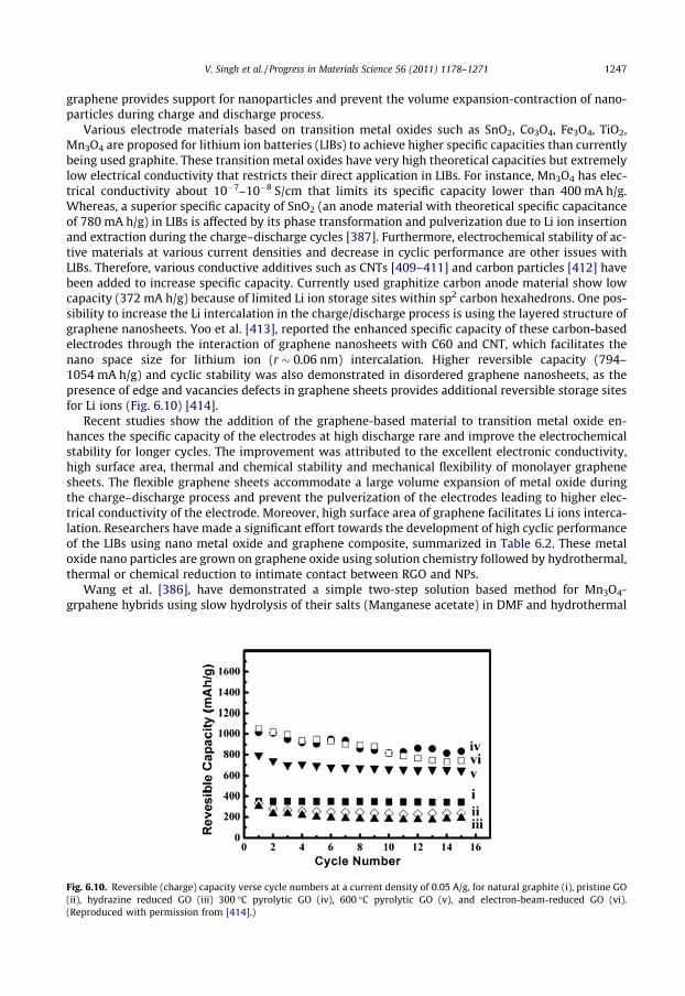
V. Singh et al. / Progress in Materials Science 56 (2011) 1178–1271 1247
graphene provides support for nanoparticles and prevent the volume expansion-contraction of nano-particles during charge and discharge process.
Various electrode materials based on transition metal oxides such as SnO2, Co3O4, Fe3O4, TiO2,Mn3O4 are proposed for lithium ion batteries (LIBs) to achieve higher specific capacities than currentlybeing used graphite. These transition metal oxides have very high theoretical capacities but extremelylow electrical conductivity that restricts their direct application in LIBs. For instance, Mn3O4 has elec-trical conductivity about 10�7–10�8 S/cm that limits its specific capacity lower than 400 mA h/g.Whereas, a superior specific capacity of SnO2 (an anode material with theoretical specific capacitanceof 780 mA h/g) in LIBs is affected by its phase transformation and pulverization due to Li ion insertionand extraction during the charge–discharge cycles [387]. Furthermore, electrochemical stability of ac-tive materials at various current densities and decrease in cyclic performance are other issues withLIBs. Therefore, various conductive additives such as CNTs [409–411] and carbon particles [412] havebeen added to increase specific capacity. Currently used graphitize carbon anode material show lowcapacity (372 mA h/g) because of limited Li ion storage sites within sp2 carbon hexahedrons. One pos-sibility to increase the Li intercalation in the charge/discharge process is using the layered structure ofgraphene nanosheets. Yoo et al. [413], reported the enhanced specific capacity of these carbon-basedelectrodes through the interaction of graphene nanosheets with C60 and CNT, which facilitates thenano space size for lithium ion (r � 0.06 nm) intercalation. Higher reversible capacity (794–1054 mA h/g) and cyclic stability was also demonstrated in disordered graphene nanosheets, as thepresence of edge and vacancies defects in graphene sheets provides additional reversible storage sitesfor Li ions (Fig. 6.10) [414].
Recent studies show the addition of the graphene-based material to transition metal oxide en-hances the specific capacity of the electrodes at high discharge rare and improve the electrochemicalstability for longer cycles. The improvement was attributed to the excellent electronic conductivity,high surface area, thermal and chemical stability and mechanical flexibility of monolayer graphenesheets. The flexible graphene sheets accommodate a large volume expansion of metal oxide duringthe charge–discharge process and prevent the pulverization of the electrodes leading to higher elec-trical conductivity of the electrode. Moreover, high surface area of graphene facilitates Li ions interca-lation. Researchers have made a significant effort towards the development of high cyclic performanceof the LIBs using nano metal oxide and graphene composite, summarized in Table 6.2. These metaloxide nano particles are grown on graphene oxide using solution chemistry followed by hydrothermal,thermal or chemical reduction to intimate contact between RGO and NPs.
Wang et al. [386], have demonstrated a simple two-step solution based method for Mn3O4-grpahene hybrids using slow hydrolysis of their salts (Manganese acetate) in DMF and hydrothermal
Fig. 6.10. Reversible (charge) capacity verse cycle numbers at a current density of 0.05 A/g, for natural graphite (i), pristine GO(ii), hydrazine reduced GO (iii) 300 �C pyrolytic GO (iv), 600 �C pyrolytic GO (v), and electron-beam-reduced GO (vi).(Reproduced with permission from [414].)

Table 6.2Graphene based lithium ion battery materials and properties.
Material Energy density(mA h/g)
Current density(mA/g)
Cycles References
Graphene encapsulated-Co3O4 1000–1100 74 �130 [378]Graphene anchored Co3O4 935 50 �30 [415]Graphene–Mn3O4 730–780 400 �50 [386]Free Mn3O4 115–300 40 �10 [386]Pure Co3O4 900 [416]SnO2–graphene 625 10 �10 [417]Pure SnO2 782 [418]Graphene-wrapped Fe3O4 1026 35 �30 [419]
580 700 �100Anatase TiO2-FGS 160 �100 (at 1C charge/
discharge rates)[388]
Rutile TiO2-FSG 170Graphene–Si 2200 – �50 [420]
1500 �200Graphene nanosheets 290 50 �20 [413](GNS) GNS + C60 600 50 20GNS + CNT 480 50 20Disordered graphene 794–1054 – – [414]Graphene–SnO2 (nanoporous
electrode)810 50 �30 [387]
Pure graphite 372 – – –
1248 V. Singh et al. / Progress in Materials Science 56 (2011) 1178–1271
treatment for reduction of GO in to RGO. The slow hydrolysis has shown the uniform distribution ofthe nano particles on RGO sheets, resulting enhanced capacity at various current density (Fig. 6.11).
To avoid the aggregation of nanoparticles during the charge–discharge cycle, a new strategy con-sisting encapsulation of metal oxide particles by graphene sheets was developed (Fig. 6.12) [378]through the co-assembly of negatively charged graphene oxide with positively charged oxide nano-particles using electrostatic attraction. The resultant composite has shown very high reversible capac-ity (1100 mA h/g in first 10 cycles) for graphene-encapsulated Co3O4 and 1000 mA h/g after 130cycles.
The functionalization of hydrophobic graphene sheets before mixing with the hydrophilic oxidenanoparticles is an another excellent approach to form a uniform metal oxide coating [388]. Theuse of anionic surfactant (i.e., sodium dodecyle sulfate) helps in dispersing individual graphene sheetsand in situ crystallization of metal oxide particles. TiO2/RGO composites were prepared for LIBs elec-trodes using surfactant assisted growth of nanoparticles of TiO2 and showed the more than doublespecific capacity than control rutile TiO2 at a high discharge rate of 30 C [388]. The ternary self-assembly approach has been used to prepare well controlled and ordered metal oxide (SnO2, SiO2,NiO, MnO2)/graphene nanocomposites includes self-assembly of metal oxides, surfactants, and graph-ene for LIB electrodes. The high concentration of RGO (30–60 wt%) with anionic surfactant has beenused to build layered metal oxide–graphene composite film electrolyte (Fig. 6.13) [417].
The controlled growth of TiO2 on graphene oxide sheets was achieved by limiting the rate of hydro-lysis during synthesis without surfactants [385]. The TiO2-RGO composite showed superior photocat-alytic activity than a variety of other TiO2 materials. Furthermore, study is not limited to the inorganicoxide particles–graphene composite. Recently, nitrogen doped graphene was also tried for the LIBs an-ode fabrication [53].6.2.2.2.2. Supercapacitors. Supercapacitors or ultra capacitors are passive and static electrical energystorage devices for short load cycle applications. Supercapacitors with very high power density, fastcharge/discharge ability without degradation and burst release characteristic makes them ideal can-didates for applications in mobile electronic gadgets and hybrid electric automobiles.
Energy stored in supercapacitor is through the ion adsorption at the electrode interface whichmake electrical double layer (electrical double layer capacitors, EDLC) or due to electron transfer be-tween the electrolyte and the electrode through fast Faradic redox reactions (psuedocapacitors). Sev-eral supercapacitor materials have been studied to enhance specific capacitance and power density.

Fig. 6.11. Electrochemical characterizations of a half-cell composed of Mn3O4/RGO and Li. The specific capacities are based onthe mass of Mn3O4 in the Mn3O4/RGO hybrid. (a) Charge (red) and discharge (blue) curves of Mn3O4/RGO for the first cycle at acurrent density of 40 mA/g. (b) Representative charge (red) and discharge (blue) curves of Mn3O4/RGO at various currentdensities. (c) Capacity retention of Mn3O4/RGO at various current densities. (d) Capacity retention of free Mn3O4 nanoparticleswithout graphene at a current density of 40 mA/g. (Reproduced with permission from [386].)
Fig. 6.12. (A) SEM and, (B) TEM images of graphene-encapsulated silica spheres. (Reproduced with permission from [378].)
V. Singh et al. / Progress in Materials Science 56 (2011) 1178–1271 1249
Among them carbon based materials such as activated carbons, carbon fibers and CNTs have beenextensively investigated as an electrode material for EDL supercapacitors owing to their good electri-cal conductivity, chemical and mechanical stability, long cycle life, and highly modifiable nanostruc-tures [421–424]. Whereas, materials such as,

Fig. 6.13. Schematic illustrations of the ternary self-assembly approach to ordered metal oxide–graphene nanocomposites. (a)Graphene or graphene stacks, which are used as the substrate instead of graphite. Adsorption of surfactant hemimicelles on thesurfaces of the graphene or graphene stacks causes its dispersion in surfactant micelles in an aqueous solution. (b) The self-assembly of anionic sulfonate surfactant on the graphene surface with oppositely charged metal cation (e.g., Sn2+) species andthe transition into the lamella mesophase toward the formation of SnO2 graphene nanocomposites, where hydrophobicgraphenes are sandwiched in the hydrophobic domains of the anionic surfactant. (c) Metal oxide–graphene layerednanocomposites composed of alternating layers of metal oxide nanocrystals and graphene/graphene stacks after crystallizationof metal oxide and removal of the surfactant. (d) Self-assembled hexagonal nanostructure of metal oxide precursor (e.g.,silicate) with nonionic surfactants (e.g., Pluronic P123) on graphene stacks. (Reproduced with permission from [417].)
1250 V. Singh et al. / Progress in Materials Science 56 (2011) 1178–1271
RuO2 and MnO2 and polymer are promising for psuedocapacitors. Various graphene-based supercapacitor materials are summarized in Table 6.3.
Supercapacitors store charge electrostatically by the adsorption of ions onto electrodes that havehigh accessible specific surface area. Therefore, a high specific capacitance active electrode plays a vi-tal role in efficient energy storage. Various forms of porous carbon, for instance CNT [433–436], mes-oporous carbon [437], activate carbon [438] and carbide derived carbon [439] have been studied forelectrodes in this respect. A new class of material e.g. graphene and RGO, have also been predictedas a potential candidate for supercapacitor electrodes due to very high specific surface area(2675 m2/g), chemical stability, excellent electrical, thermal conductivity and capacitance and lowcost [331,425,427,440]. Interestingly, graphene has demonstrated the intrinsic capacitance near21 lF/cm2, that set new upper limit for capacitance [441]. Ruoff and coworkers [425], pioneeredthe application of chemically reduced graphene in supercapacitor. They have shown CRG’s potentialas an electrode for super capacitor, even though the used surface area was 707 m2/g and graphenesheets were not fully accessible by the electrolyte. The supercapacitor had specific capacitances of135 F/g and 99 F/g in aqueous KOH and organic electrolytes, respectively. Improved capacitance(191 F/g, in KOH) was obtained after using microwave power to expand GO layers and reduce the

Table 6.3Graphene based supercapacitor materials and properties.
Material SpecificCapacitance(F/g)
EnergydensityPowerdensity
Electrolyte References
Chemically reduced GO 135 Aqueous KOH [425]99 Organic electrolyte
Graphene–hydrous RuO2
(38.3 wt%)570 20.1 W h/kg
at 100 mA/g1 M H2SO4 [399]
10 kW/kg at4.3 W h/kg
Graphene (2675 m2/g) 550Graphene (microwave assisted
reduction of GO)191 At 150 mA/
g dischargecurrent
5M KOH electrolyte [442]
Thermal reduction in propylenecarbonate
120 Organic electrolyte [426]
Graphene (hydrazine reduced GO) 205 28 W h/kg KOH [427]10 kW h/g
Graphene–PANI (50:50 wt%)(microwave-solvothermal)
408 1 M H2SO4 [428]
Graphene–PANI (in situ anodicelectro-polymerization of PANIfilm on graphene paper)
233 – [363]
Graphene–PANI 1046 6 M KOH [363]Graphene–MnO2 216 1 M Na2SO4 [429]Polymer modified graphene
sheet + MWCNT120 – [430]
Curved Graphene Sheets 100–250 atcurrentdensity 1 A/g
85.6 W h/kgat 1 A/g
1-Ethyl-3-methylimidazoliumtetrafluoroborate
[431]
Thermally reduced graphene 75 F/g 31.9 W h/kg N-butyl-N-methylpyrrolidiniumbis(trifluoromethanesulfonyl)imide(PYR14TFSI)
[421]
117 F/g – H2SO4
MnO2 nanowire–graphene 31 F/g 30.4 W h/kg Neutral aqueous Na2SO4 [432]
V. Singh et al. / Progress in Materials Science 56 (2011) 1178–1271 1251
GO to RGO (surface area �463 m2/g) [442]. Wang et al. [427] have achieved specific capacitance value�205 F/g for hydrazine reduce GO of effective surface area �320 m2/g. It is worth noting that the sur-face area of graphene sheets plays a significant role which directly affects the performance of thesupercapacitors.
A main drawback of using graphene and RGO is the agglomeration and restacking due to Van derWaals attraction between the neighboring sheets. The aggregation reduces the effective surface arearesulting loss of capacitance. Therefore, a few researchers have made effort to keep graphene sheetsseparated by addition of metal oxide nanoparticles [399]. Metal oxide RuO2, MnO2 and polyaniline(PANI), nano composite with graphene have also been explored for superior capacitance (Table 6.3).The approach utilizing nanoparticles to improve the electrochemical performance is an indication ofa positive synergistic effect of graphene sheets and nanoparticles. For example, in RuO2/graphenecomposite, graphene sheets were well separated by RuO2 nanoparticles that were attached throughthe oxygen containing functional groups on graphene surfaces. The composite exhibited a high spe-cific capacitance of 570 F/g for 38.3% Ru loading with excellent electrochemical stability (97.9% reten-tion after 1000 cycles) and high energy density (20.1 W h/kg) at high power density (10 kW/kg).Similarly, MnO2/GO composite electrode had a capacitance of 216 F/g that is much higher than thatof individual GO (10.9 F/g) and bulk MnO2 (6.8 F/g) [429]. Wu, et al. [432], demonstrated a MnO2/graphene high voltage asymmetric capacitor based on graphene as a negative electrode and MnO2/graphene composite a positive electrode, which exhibited a superior energy density of 30 kW/kgand power density (5 kW/kg at 7 W h/kg). Although the metal oxide–graphene nano composite have

1252 V. Singh et al. / Progress in Materials Science 56 (2011) 1178–1271
shown a great prominence for the supercapacitors and high energy density capacitor, the high energydensity supercapacitors with high charge/discharge rates are still up to research stage. Recent study ofJang and coworkers [431] reveals the graphene-based supercapacitor that exhibits specific energydensity of 85.6 W h/kg at room temperature and 136 W h/kg at 80 �C at very high current densityof 1 A/g. These values are comparable to Ni metal hydride (40–100 W h/kg). They have reported thatthe mesoporous structure of the curved graphene sheet are responsible, the curved nature of graphenesheets prevent face to face restacking and maintain large pore size (2–25 nm) and capacitance(Fig. 6.14). Further quick charge–discharge ability in seconds and minimal loss of capacity or energydensity make it prominent candidate better than existing batteries.
Recently, graphene–polymer composites have also received much attention owing to their flexibil-ity, and superior capacitance than existing carbon-polymer based capacitor. Among various conduc-tive polymers, PANI has been considered as a most promising conductive electrode material andstudied considerably with CNT and carbon system [367,369,443–446]. A graphene nanosheets–PANIcomposite was synthesized by in situ polymerization [367]. The specific capacitance of 1046 F/gwas obtained at a scan rate of 1 mV/s. Conductive graphene nanosheets provide more active sitesfor nucleation of PANI and is homogeneously coated by PANI nano particles on both sides, resultingin energy density of 39 kW h/g at a power density of 70 kW/kg. Graphene–PANI composite paperwas also prepared by in situ anodic electropolymerization of polyaniline film on graphene paper(Fig. 6.15) [363]. The flexible as prepared composite paper combined the high conductivity and flex-ibility properties of graphene sheet with large capacitance polymer and showed the gravimetriccapacitance of 233 F/g.
6.2.2.3. Other applications. Fuel cells are considered as one of the most promising power sources for themobile and stationary applications due to their high energy conversion efficiency, low operating tem-perature and ease of handling. Pt and Pt based materials are widely used for the fuel cell, which ren-ders them ineffective and prevents fuel oxidation. Recently, graphene based materials have beenexplored for fuel cell applications [447–449]. The proton exchange membrane (PEM) fuel cells proto-type using graphene was developed by Serger et al. [448]. They constructed using a Toray paper mod-ified with RGO/Pt composites as a cathode and Pt-dispersed on carbon black as an anode. Theperformance of the fuel cell was compared to unsupported Pt cathode PEM (Fig. 6.16).
The RGO/Pt-based fuel cell showed a maximum power of 161 mW/cm2 compared to 96 mW/cm2
for an unsupported Pt-based fuel cell. The role of graphene support not only maximized the availabil-ity of electrocatalyst surface area for electron transfer but also provided better mass transport of reac-tants to the electrocatalyst.
Fig. 6.14. Scanning electron microscopy image of curved graphene sheets (scale bar 10 lm). (Reproduced with permission from[431].)

Fig. 6.15. Digital camera images of (left) two freestanding G-papers (30 mm, 10 mm) and (right) a flexible G-paper.(Reproduced with permission from [363].)
Fig. 6.16. Galvanostatic fuel cell polarization (I–V) curves (a–c) and power characteristics (a0–c0) of a fuel cell at 60 �C and 1 atmof back pressure. The cathode composed of (a and a0) Pt, (b and b0) 1:1 GO-Pt, and 1:1 GO-Pt (hydrazine, 300 �C treated).Electrocatalyst concentration maintained at 0.2 mg/cm2 Pt. (Reproduced with permission from [448].)
V. Singh et al. / Progress in Materials Science 56 (2011) 1178–1271 1253
For biological applications of GO/RGO, RGO-based single-bacterium biodevice, label-free DNA sen-sor, bacterial DNA/protein and polyelectrolyte chemical transistor have been reported [99]. Liu et al.observed that the GO sheets are biocompatible without obvious toxicity and employed GO for drugdelivery [97]. One of the promising targeting methods is the use of magnetic particles loaded withdrugs. Thus, magnetic NPs with graphene composites have been used in various areas of drug carrierand magnetic resonance imaging (MRI) [284,376,377,450]. The magnetization curve of GO–Fe3O4
composite was measured at room temperature (Fig. 6.17) showed a magnetic hysteresis loop of ‘‘S’’line curve with nearly zero value of the magnetic remanence. This suggested that GO–Fe3O4 exhibiteda superparamagnetic behavior.
Myung et al. reported the assembly of Au NPs fabricated on top of a reduced GO junction [404]. Atthe crossing point the forward bias from �10 to 10 V (or reverse bias from 10 to �10 V) sweep curvesshowed a positive (or negative) slope indicating an n-type (or p-type) FET behavior (Fig. 6.18a). It indi-cates that in the forward sweep, charges move along in n-type channels (right of Fig. 6.18b). While, inreverse sweep, charge transfer shows p-type characteristics left of Fig. 6.18b. These properties

Fig. 6.17. Magnetization curve of GO–Fe3O4 hybrid. (Reproduced with permission from [376].)
Fig. 6.18. ‘‘Type-switching’’ memory devices and reconfigurable logic circuits. (a) Typical hysteresis curve of type-switchingmemory device based on GO and NPs. It exhibited both n-type and p-type characteristics near zero gate bias voltage. (b)Operation principle of type-switching memory device. (Reproduced with permission from [404].)
1254 V. Singh et al. / Progress in Materials Science 56 (2011) 1178–1271
suggested that the metal NPs based graphene device can be operated as a conventional conductiveswitching memory by adjusting the charge density on the metal NPs.
Despite the rapid increase of research on chemically functionalized graphene-based NPs composite,there is lack of theoretical understanding of charge transport studies. Therefore, theory based trans-port studies with energy band are strongly encouraged in pristine graphene [451,452].
7. Toxicity of graphene/graphene oxide/reduced graphene oxide
Recent advancement in nanoscience opens a wide range of applications of nanoparticles towardsindustrial level as well as in medicine. Nanoparticles exhibit extraordinary physiochemical propertiesand reflect their unique electrical, thermal, and mechanical properties which further bring along a con-cern about their toxic behavior when exposed to the environment and living system. In the near, thefuture potential occupational and public exposure to the nanoparticles will be dramatically increaseddue to the versatile applications of nanomaterials [453]. In the recent years government and scientific

V. Singh et al. / Progress in Materials Science 56 (2011) 1178–1271 1255
communities put forward more attention towards the bio-safety aspect of the nanomaterials. The mainagenda in the field of nanotoxicology is to understand the exposure and assessment of nanoparticles,environmental and biological fate, transport, persistence, transformation, recyclability and overall sta-bility of the nanoparticles [453]. For example, though carbon nanotubes (CNTs) were an exceptionalscientific finding in the field of electronics; its wide use allows potential exposure to the environmentand living systems. Several reports have revealed that the CNTs could induce genotoxicity via inductionof reactive oxygen species (ROS) [454,455]. Similarly, graphene and graphene oxide are now very muchattractive due to their potential applications such as electrochemical devices, energy storage, and catal-ysis, adsorption of enzyme, cell imaging, drug delivery, and biosensors. However, information related tothe long term fate, health, and environmental risk assessment of this newly discovered graphene iswidely lacking [456].
RGO’s good conductive property has a potential for developing various bio-medical applicationsincluding biosensor, transplant devices, invasive instruments, and implants [457]. RGO and RGO-Tween 20 paper like composites have been studied for their toxicological aspects. In vitro experi-ments with mouse fibroblast cell shows no toxicity of RGO paper [458]. Though surface of theRGO-Tween 20 composite is electrically insulating, RGO-Tween 20 composite also reported to benon-toxic towards Vero cells, bovine embryonic cells and Crandell–Rees feline kidney cells [457].In contrast to this report, GO-nanosheets reported to be toxic to the bacterial cell [459]. GO-nano-sheets showed 60% and 70% cell viability decrease in Escherichia coli and Staphylococcus aureus,respectively. Toxicity of graphene nanosheets towards the E. coli has also been reported [460]. Met-abolic activity of the E. coli decreased to 13% when incubated with 85 lg/ml GO nanosheets. More-over, bacterial cell viability loss was almost 98.5% in the same concentration. A transmissionelectron microscope study revealed disruption of the bacterial cell membrane and a loss of mem-brane integrity. Therefore, it may be concluded that the toxicity of graphene oxide nanosheetsmainly attributed to the mechanical damage of the cell membrane of the bacteria due to the sharpedges of the nanosheets. Moreover, hydrazine reduced GO nanosheets were reported to be moretoxic to the bacterial cell, may be due to the better charge transfer efficiency in addition to theirsharp edges [459].
In the in vitro mammalian cell line experiment, the cytotoxic effect of GO was found to be dose andtime dependent, even at a concentration of less than 20 lg/ml. Above 50 lg/ml, GO severely affectsthe cell survival rate and induces apoptosis in human fibroblast cell line [456]. Alteration of cellularmorphology by GO treated fibroblast cell is shown in Fig. 7.1.
Similar cytotoxic effects were also observed in other cell lines such as MGC803, MCF-7, MDA-MB-435, and HepG2. Experimental data also demonstrates that the GO enters into the cytoplasm of thecell and was found to be present in the sub cellular compartments such as lysosomes, mitochondrion,endoplasm, and even in the nucleus. It has been hypothesized that GO attaches to the cell membraneand induces down regulation of the adhesion associated gene which in turns affect the cell adhesionand causing cell to float in medium. Moreover, GO enters into the cell and can interfere with cellularmetabolism and finally results in cell apoptosis and death [456]. In a recent report, the toxicologicaleffect of CNTs and graphene nanomaterial towards neuronal PC12 cells are compared [454]. Relativetoxicity of graphene nanostructure is less as compared to CNTs. The 100 lg/ml of the graphene signif-icantly increases the ROS generation and lactate dehydrogenase release, which are markers of celldeath via necrosis. The reports further document that the shape and size of graphene play a criticalrole in evaluating the toxicity caused by graphene. Concentrations and size of the GO used to evaluatein vitro cytotoxicityy are summarized in Table 7.1.
Recently, the size effect of the GO towards cytotoxicity has been reported [461]. The cytotoxicity ofsmaller size GO (160 ± 90 nm) was found to have higher values compared to larger size GO nanosheets(430 ± 300 nm and 780 ± 410 nm). Smaller size GO also induced apoptosis to the A549 cell at a con-centration of 200 lg/ml. Though apoptosis was not observed in the presence of larger GO nanosheets(780 ± 410 nm), a slight increase in necrosis was noticed. Medium size GO nanosheets neither showedapoptosis nor necrosis towards A549 cells. A similar effect was observed on the cell viability and thecell mortality was observed in the following order; 160 ± 90 nm size nanosheets >780 ± 410 nm nano-sheets >430 ± 300 nm nanosheets. The nanosheets of size 430 ± 300 nm showed a significant decreasein cell viability only at 200 lg/ml concentration, whereas 160 ± 90 nm and 780 ± 410 nm size nano-

Fig. 7.1. Morphology of human fibroblast cell line in GO treated and control cell; A-Control, B-100 lg/ml for 1 day; C-20 lg/mlfor 3 days; D-5 lg/ml 5 days. (Reproduced with permission from [456].)
Table 7.1Size, concentration, and cytotoxicity of GO nanosheet.
Size range Concentration(lg/ml)
Intra-cellularlocalization
Cell/cell line Toxic concentration(lg/ml)
References
1–2 lm 5–100 Lysosomes,mitochondrion,endoplasm, andnucleus
Human fibroblast cell,MGC803, MCF-7,MDA-MB-435, andHepG2 cell lines
50 [456]
3–5 nm 0.1–100 – PC12 cells 100 [454]70–250 nm 10–200 Hardly localized
inside the cellA549 50 [461]
130–730 nm 10–200 Hardly localizedinside the cell
A549 200 [461]
370–1190 nm 10–200 Hardly localizedinside the cell
A549 50 [461]
100–700 nm 20–85 Endosome A549 85 [460]100–700 nm 20–85 – E. coli 85 [460]
1256 V. Singh et al. / Progress in Materials Science 56 (2011) 1178–1271

V. Singh et al. / Progress in Materials Science 56 (2011) 1178–1271 1257
sheets showed a decrease at a concentration of 50 lg/ml. The reduction in cell viability has been cor-related to oxidative stress which is generated by GO nanosheets. It has also been found that the GOnanosheets generate reactive oxygen species in cell free F–12 K medium, which is further supportedby the oxidative stress, induced cell viability reduction. The extent of reactive oxygen species gener-ation is 50% higher in 780 ± 410 nm size nanosheets as compared to 160 ± 90 nm and 430 ± 300 nmsize nanosheets. However, cell proliferation in the GO film was found to be similar as control andno cellular internalization of graphene nanosheets was observed. Therefore it can be concluded thatthe oxidative stress induced to the cells by GO nanosheets is due to external generation of reactiveoxygen species.
The in vivo study in mice model does not show any toxicity at a dose 60.25 mg per mouse. How-ever, 0.4 mg per mouse was found to be lethal to the mouse, and all four mice died within 1–7 daysof GO injection. Histopathology of the lung tissues showed a blocking of the major airways by theGO conglomeration. Moreover, a loss of 10% body weight was observed within the 1st week of theGO injection. Long term stay of the GO in kidney makes it a very poor agent for in vivo application,although GO has been investigated as a cellular imaging and drug delivery agent. It is a challenge toreduce the toxicity effect of the GO and successfully use GO for medical applications. Therefore,graphene has been tried to conjugate with biocompatible polymer such as polyethylene glycol(PEG) and chitosan, for safe bio-medical application. The graphene functionalized with PEG showsa better solubility and stability in physiological solution and has been studied for in vitro drug deliv-ery, imaging, and in vivo photothermal therapy for tumor. In vitro experiments with PEG function-alized GO do not show any cytotoxicity towards HCT-116 cell line [97]. No toxic side effect wasreported in the case of PEG functionalized GO in in vivo mice model at a dose of 20 mg/kg of thebody weight, however an excellent passive targeting of the tumor was achieved. Moreover, haema-toxylin and eosin stained organ slices did not reveal any organ damage. The tumor disappeared inthe mice received PEG functionalized GO after 1 day of photothermal therapy and no tumor growthwas noticed within 40 days time [462]. However, there is always a chance of quenching the fluores-cence (Cy7) which may leads to in inaccurate conclusion regarding the bio-distribution. The samegroup has conducted a similar kind of study with 125I labeled PEG–GO for in vivo pharmacokinetics,bio-distribution and toxicological study. Stability of the 125I labeled PEG–GO was confirmed by incu-bating the 125I labeled PEG–GO in 0.9% NaCl solution, mouse plasma and serum at 37 �C. 125I labeledPEG–GO was injected intravenously and radioactive levels in the blood were estimated over times.PEG–GO followed a two component blood circulation model with a half life of 0.39 ± 0.097 h for thefirst phase and 6.97 ± 0.62 h for the second phase. PEG–GO was found to be accumulated mainly inthe liver, kidneys, and spleen, however, accumulation in bone marrow was also observed at the earlyin the experiments. Radioactivity level measurement and histology analysis of the organs revealedthat with time, accumulated PEG–GO cleared out from the organs like the liver, kidneys and spleen.PEG–GO was excreted from the body though renal and fecal excretion which also reflectd the kidneyand intestine uptake of PEG–GO. Body weight loss or toxic side effects were not observed within the3 months after the introduction of PEG–GO. Moreover, blood biochemistry, hematological and histo-logical analysis did not reveal any potential toxic effects [463]. Besides the PEG–graphene study,graphene–chitosan composites have also been studied for tissue engineering application; they arereported to be biocompatible [333]. Recently, few other polymers were tried to reduce graphenetoxicity towards living cells and to make it more compatible for bio-medical use. The 3,4,9,10-perylene tetracarboxylic acid (PTCA) is one of them, PTCA functionalized graphene sheets did notshow any significant toxicity towards HeLa cells. PTCA–graphene and aptamer AS1411 sensor havebeen successfully shown to differentiate cancer and normal cells [464]. Graphene–polyethylenimine(PEI) composite also found to be less toxic towards HeLa cells as compared to graphene alone. More-over, graphene–PEI nanocomposite has been demonstrated as an efficient gene transfection vehicle[465].
Controversial reports exist on cytotoxicity of the graphene/GO/RGO which restricts their potentialbio-medical applications. This may be associated with the different preparation, size of the sheets andthe functionalization. Therefore, thorough toxicology studies of functionalized and bare graphene/GO/RGO at different doses using different animal model is necessary before any potential bio-medicalapplications.

1258 V. Singh et al. / Progress in Materials Science 56 (2011) 1178–1271
8. Future prospects
It has become evident that the exceptional properties of graphene (including electrical, thermal,mechanical, optical, and long electron mean free paths) made it compelling for various engineeringapplications. Much effort has been devoted to exploring the fundamental physics and chemistry ofgraphene. Novel properties such as room temperature quantum Hall effect, highest charge transportand thermal conductivity originated from graphene’s 2-dimensional structures have not been ob-served earlier from most conventional three-dimensional materials. A large amount of research pub-lications in the past 5 years signifies the importance of graphene that might surpass silicon research inthe development of microelectronics. While silicon based research is at its mature stage to overcomethe technological barrier, graphene is being extensively investigated as it holds the future for micro tonano scale electronics. The inherent semi-metal characteristic of graphene has been modified to real-ize the applications in transistors. Graphene nanoribbons and bilayer graphene are the results of suchmodification that leads to a suitable band gap and allows the applications in FET. However, grapheneas a new material still faces many challenges ranging from synthesis and characterization to the finaldevice fabrication. The exceptional properties were observed in the defect free pristine graphene pre-pared by graphite exfoliation using scotch tape method which is not appropriate for any large scaledevice manufacturing. The alternative methods have progressed to CVD and epitaxially grown single,bilayer and few-layer graphene. Recent reports demonstrated the scalability using CVD method to wa-fer scale on different substrates and facile transfer of graphene layer for subsequent device fabrication.These breakthroughs offer novel and exciting opportunities for semiconductor industries. The chem-ical exfoliation of graphite into GO followed by thermal and chemical reduction, has offered a cost-effective production route of reduced graphene oxide on a large scale. However, the chemical andthermal modification lowers the electrical and mechanical properties, along with its chemical reactiv-ity leading to lack of control in functionalization by other groups. The controlled oxidation/reductionand functionalization are very important in tuning the material properties such as band gap, electricalconductivity, and mechanical properties. Therefore, controlled modification of graphite, GO, and RGOis crucial in expanding the applications of graphene-based materials. In addition, the large surface oflow density GO and RGO in mass production may possess handling difficulty, which can lead to ahealth risk due to inhaling and handling toxic reducing chemicals. The health risk associated withgraphene and their derivatives needs to be evaluated through the investigation of the toxicity and bio-compatibility of these novel carbon structures and its derivatives.
The possible applications of graphene-based material include transparent flexible electrodes,graphene/polymer composites for mechanical parts, energy storage, sensors and organic electronics.Graphene/polymer composites have showed the lowest percolation threshold for electrical conductiv-ity and improved mechanical, thermal, and gas barrier properties. However, the core issues such as thehomogeneous distribution of individual graphene platelets, their orientation, connectivity, and inter-face bonding with matrix still require more investigation. The charge mobility of RGO is considerablyhigher than that of the amorphous silicon and existing semi-conducting conjugated polymers, enlight-ening the probable path for the application in electronics. The main hurdles with any device fabrica-tion using RGO including defects at atomic level, the folding/wrinkling of RGO and the over lapping ofRGO at macro-scale require continuous research endeavors.
The visibility of monolayer graphene under an optical microscope requires the suitable substrate tocreate contrast between different layers due to interference. Current detection of graphene using anoptical microscope depends on the substrate thickness and incident light wavelength. More researchis needed to develop a simple detection method of pristine graphene that is independent of supportmaterial. Aberration corrected high resolution TEM made it possible to reveal defect structures andgraphene quantum dot at atomic resolutions, providing opportunities to visually examine the dopingand defects at atomic levels.
Although the advanced deposition technique of single layer and bilayer made it possible to fabri-cate large area devices, creating band gap in a controlled and practical manner is still challenging forthe application in logic devices. Several methods aiming at tuning the substrates properties and nano-ribbon dimension have been proposed to introduce tunable band gap essential for nanoelectronics.

V. Singh et al. / Progress in Materials Science 56 (2011) 1178–1271 1259
Particularly, this energy band gap can be achieved through quantum confinement, bilayer graphene,and chemical functionalization. The former, quasi-one-dimensional graphene nanoribbon has beenconsidered with either edge localization or Coulomb blockade effects. Graphene nanoribbon withappropriate dimension (i.e. 10 nm) is expected to provide right band gap for efficient FET devices.
Cutting graphene into nanoribbon has shown great promise for FET logic applications, but associ-ated with the electron scattering at the rough edges and disorder from the back substrate. On the otherhand, FETs based on graphene bilayer still require large on/off ratio for logic applications. The new op-tions such as tunnel FETs and bilayer pseudospin FETs have been suggested to tackle the challenge ofthe graphene devices problems based on the conventional FET principle. These concepts are supportedby simulation studies but need to be experimented. The latter, oxides form of graphene (GO), has trig-gered significant research interest due to large scale integration. However, the electronic band struc-ture is not clearly understood due to the nanoscale inhomogeneity. Recent atomic scale systematicalinvestigation and geometrical microscopic studies provided the evidence of tunable band gap throughvarying oxidation level and reduction process. Therefore band gap opened graphene based throughGNR and GO have been encouraged to become future practical nano electronic devices comparableto complementary metal oxide semiconductor circuits.
Acknowledgements
This work is supported by the National Science Foundation for nanotechnology research. Weacknowledge the financial support obtained from NSF: ECCS 0748091, ECCS 0801924, and NSF:DMR 0746499 and CBET 0930170. Authors would like to acknowledge editors for their valuable com-ments and suggestions on the articles.
References
[1] Slonczewski JC, Weiss PR. Band structure of graphite. Phys Rev 1958;109:272.[2] Zhang YB, Tan YW, Stormer HL, Kim P. Experimental observation of the quantum Hall effect and Berry’s phase in
graphene. Nature 2005;438:201.[3] Novoselov KS, Jiang Z, Zhang Y, Morozov SV, Stormer HL, Zeitler U, et al. Room-temperature quantum Hall effect in
graphene. Science 2007;315:1379.[4] Novoselov KS, Geim AK, Morozov SV, Jiang D, Katsnelson MI, Grigorieva IV, et al. Two-dimensional gas of massless Dirac
fermions in graphene. Nature 2005;438:197.[5] Novoselov KS, Geim AK, Morozov SV, Jiang D, Zhang Y, Dubonos SV, et al. Electric field effect in atomically thin carbon
films. Science 2004;306:666.[6] Balandin AA, Ghosh S, Bao W, Calizo I, Teweldebrhan D, Miao F, et al. Superior thermal conductivity of single-layer
graphene. Nano Lett 2008;8:902.[7] Lee C, Wei X, Kysar JW, Hone J. Measurement of the elastic properties and intrinsic strength of monolayer graphene.
Science 2008;321:385.[8] Wu J, Becerril HA, Bao Z, Liu Z, Chen Y, Peumans P. Organic solar cells with solution-processed graphene transparent
electrodes. Appl Phys Lett 2008;92:263302.[9] Li X, Wang X, Zhang L, Lee S, Dai H. Chemically derived, ultrasmooth graphene nanoribbon semiconductors. Science
2008;319:1229.[10] Ritter KA, Lyding JW. The influence of edge structure on the electronic properties of graphene quantum dots and
nanoribbons. Nat Mater 2009;8:235.[11] Ubbelohde AR, Lewis LA. Graphite and its crystal compounds. London: Oxford University Press; 1960.[12] Thompson TE, Falardeau ER, Hanlon LR. The electrical conductivity and optical reflectance of graphite–SbF5 compounds.
Carbon 1977;15:39.[13] Fuzellier H, Melin J, Herold A. Conductibilité électrique des composés lamellaires graphite–SbF5 et graphite–SbCl5.
Carbon 1977;15:45.[14] Shenderova OA, Zhirnov VV, Brenner DW. Carbon nanostructures. Crit Rev Solid State Mater Sci 2002;27:227.[15] Krishnan A, Dujardin E, Treacy MMJ, Hugdahl J, Lynum S, Ebbesen TW. Graphitic cones and the nucleation of curved
carbon surfaces. Nature 1997;388:451.[16] Land TA, Michely T, Behm RJ, Hemminger JC, Comsa G. STM investigation of single layer graphite structures produced on
Pt(111) by hydrocarbon decomposition. Surf Sci 1992;264:261.[17] Nagashima A, Nuka K, Itoh H, Ichinokawa T, Oshima C, Otani S. Electronic states of monolayer graphite formed on
TiC(111) surface. Surf Sci 1993;291:93.[18] Forbeaux I, Themlin JM, Debever JM. Heteroepitaxial graphite on 6H–SiC(0001): interface formation through conduction-
band electronic structure. Phys Rev B 1998;58:16396.[19] Berger C, Song ZM, Li TB, Li XB, Ogbazghi AY, Feng R, et al. Ultrathin epitaxial graphite: 2D electron gas properties and a
route toward graphene-based nanoelectronics. J Phys Chem B 2004;108:19912.

1260 V. Singh et al. / Progress in Materials Science 56 (2011) 1178–1271
[20] Berger C, Song Z, Li X, Wu X, Brown N, Naud Cc, et al. Electronic confinement and coherence in patterned epitaxialgraphene. Science 2006;312:1191.
[21] Ohta T, Bostwick A, Seyller T, Horn K, Rotenberg E. Controlling the electronic structure of bilayer graphene. Science2006;313:951.
[22] Novoselov KS, Geim AK, Morozov SV, Jiang D, Zhang Y, Dubonos SV, et al. Electric field effect in atomically thin carbonfilms. Science 2004;306:666.
[23] Fukushima H, Drzal LT. A carbon nanotube alternative: graphite nanoplatelets as reinforcements for polymers. Annu TechConf Soc Plast Eng 2003;61:2230.
[24] kelly BT. Physics of Graphite, Applied Science, London 1981:475.[25] Kotov NA. Materials science: carbon sheet solutions. Nature 2006;442:254.[26] Stankovich S, Dikin DA, Piner RD, Kohlhaas KA, Kleinhammes A, Jia Y, et al. Synthesis of graphene-based nanosheets via
chemical reduction of exfoliated graphite oxide. Carbon 2007;45:1558.[27] Eda G, Fanchini G, Chhowalla M. Large-area ultrathin films of reduced graphene oxide as a transparent and flexible
electronic material. Nature Nanotechnol 2008;3:270.[28] Becerril HA, Man J, Liu Z, Stoltenberg RM, Bao Z, Chen Y. Evaluation of solution-processed reduced graphene oxide films as
transparent conductors. ACS Nano 2008;2:463.[29] Blake P, Brimicombe PD, Nair RR, Booth TJ, Jiang D, Schedin F, et al. Graphene-based liquid crystal device. Nano Lett
2008;8:1704.[30] Hernandez Y, Nicolosi V, Lotya M, Blighe FM, Sun Z, De S, et al. High-yield production of graphene by liquid-phase
exfoliation of graphite. Nat Nanotechnol 2008;3:563.[31] Lotya M, Hernandez Y, King PJ, Smith RJ, Nicolosi V, Karlsson LS, et al. Liquid phase production of graphene by exfoliation
of graphite in surfactant/water solutions. J Am Chem Soc 2009;131:3611.[32] Green AA, Hersam MC. Solution phase production of graphene with controlled thickness via density differentiation. Nano
Lett 2009;9:4031.[33] Kang FL, Zhang TY. Influences of H2O2 on synthesis of H2SO4-GICs. J Phys Chem Solids 1996;57:889.[34] Kang F, Zhang TY, Leng Y. Electrochemical behavior of graphite in electrolyte of sulfuric and acetic acid. Carbon
1997;35:1167.[35] Pan YX, Yu ZZ, Ou YC, Hu GH. A new process of fabricating electrically conducting nylon 6/graphite nanocomposites via
intercalation polymerization. J Polym Sci Part B – Polym Phys 2000;38:1626.[36] Li X, Zhang G, Bai X, Sun X, Wang X, Wang E, et al. Highly conducting graphene sheets and Langmuir–Blodgett films. Nat
Nanotechnol 2008;3:538.[37] May JW. Platinum surface LEED rings. Surf Sci 1969;17:267.[38] Shelton JC, Patil HR, Blakely JM. Equilibrium segregation of carbon to a nickel (111) surface: a surface phase transition.
Surf Sci 1974;43:493.[39] Eizenberg M, Blakely JM. Carbon monolayer phase condensation on Ni(111). Surf Sci 1979;82:228.[40] Somani PR, Somani SP, Umeno M. Planer nano-graphenes from camphor by CVD. Chem Phys Lett 2006;430:56.[41] Cao H, Yu Q, Colby R, Pandey D, Park CS, Lian J, et al. Large-scale graphitic thin films synthesized on Ni and transferred to
insulators: Structural and electronic properties. J Appl Phys 2010;107:044310.[42] Bhaviripudi S, Jia X, Dresselhaus MS, Kong J. Role of kinetic factors in chemical vapor deposition synthesis of uniform large
area graphene using copper catalyst. Nano Lett 2010;10:4128.[43] Kim KS, Zhao Y, Jang H, Lee SY, Kim JM, Kim KS, et al. Large-scale pattern growth of graphene films for stretchable
transparent electrodes. Nature 2009;457:706.[44] Li X, Cai W, An J, Kim S, Nah J, Yang D, et al. Large-area synthesis of high-quality and uniform graphene films on copper
foils. Science 2009;324:1312.[45] Chae SJ, Gunes F, Kim KK, Kim ES, Han GH, Kim SM, et al. Synthesis of large-area graphene layers on poly-nickel substrate
by chemical vapor deposition: wrinkle formation. Adv Mater 2009;21:2328.[46] Lee S, Lee K, Zhong Z. Wafer Scale homogeneous bilayer graphene films by chemical vapor deposition. Nano Lett
2010;10:4702.[47] Lee Y, Bae S, Jang H, Jang S, Zhu S-E, Sim SH, et al. Wafer-scale synthesis and transfer of graphene films. Nano Lett
2010;10:409.[48] Reina A, Jia X, Ho J, Nezich D, Son H, Bulovic V, et al. Large area, few-layer graphene films on arbitrary substrates by
chemical vapor deposition. Nano Lett 2008;9:30.[49] Li X, Cai W, Colombo L, Ruoff RS. Evolution of graphene growth on Ni and Cu by carbon isotope labeling. Nano Lett
2009;9:4268.[50] Bae S, Kim H, Lee Y, Xu X, Park J-S, Zheng Y, et al. Roll-to-roll production of 30-inch graphene films for transparent
electrodes. Nat Nanotechnol 2010;5:574.[51] Wei D, Liu Y, Wang Y, Zhang H, Huang L, Yu G. Synthesis of N-doped graphene by chemical vapor deposition and its
electrical properties. Nano Lett 2009;9:1752.[52] Qu L, Liu Y, Baek J-B, Dai L. Nitrogen-doped graphene as efficient metal-free electrocatalyst for oxygen reduction in fuel
cells. ACS Nano 2010;4:1321.[53] Reddy ALM, Srivastava A, Gowda SR, Gullapalli H, Dubey M, Ajayan PM. Synthesis of nitrogen-doped graphene films for
lithium battery applications. ACS Nano 2010;4:6337.[54] Wang JJ, Zhu MY, Outlaw RA, Zhao X, Manos DM, Holoway BC. Free-standing subnanometer graphite sheets. Appl Phys
Lett 2004;85:1265.[55] Wang JJ, Zhu MY, Outlaw RA, Zhao X, Manos DM, Holoway BC. Synthesis of carbon nanosheets by inductively coupled
radio-frequency plasma enhanced chemical vapor deposition. Carbon 2004;42:2867.[56] Malesevic A, Vitchev R, Schouteden K, Volodin A, Zhang L, Tendeloo GV, et al. Synthesis of few-layer graphene via
microwave plasma-enhanced chemical vapour deposition. Nanotechnolgy 2008;19:305604.[57] Vitchev R, Malesevic A, Petrov RH, Kemps R, Mertens M, Vanhulsel A, et al. Initial stages of few-layer graphene growthby
microwave plasma-enhanced chemical vapour deposition. Nanotechnolgy 2010;21:095602.

V. Singh et al. / Progress in Materials Science 56 (2011) 1178–1271 1261
[58] Zhu M, Wang J, Holoway BC, Outlaw RA, Zhao X, Hou K, et al. A mechanism for carbon nanosheet formation. Carbon2007;45:2229.
[59] Hass J, Heer WAd, Conrad EH. The growth and morphology of epitaxial multilayer graphene. J Phys: Condens Matter2008;20:323202.
[60] de Heer WA, Berger C, Wu X, First PN, Conrad EH, Li X, et al. Epitaxial graphene. Solid State Commun 2007;143:92.[61] Varchon F, Feng R, Hass J, Li X, Nguyen BN, Naud C, et al. Electronic structure of epitaxial graphene layers on SiC: effect of
the substrate. Phys Rev Lett 2007;99:126805.[62] Penuelas J, Ouerghi A, Lucot D, David C, Gierak J, Estrade-Szwarckopt H, et al. Surface morphology and characterization of
thin graphene films on SiC vicinal substrate. Phys Rev B 2009;79:033408.[63] Tedesco JT, Jernigan GG, Culbertson JC, Hite JK, Yang Y, Daniels KM, et al. Morphology characterization of argon-mediated
epitaxial graphene on C-face SiC. Appl Phys Lett 2010;96:222103.[64] Emtsev KV, Bostwick A, Horn K, Jobst J, Kellogg GL, Ley L, et al. Towards wafer-size graphene layers by atmospheric
pressure graphitization of silicon carbide. Nat Mater 2009;8:203.[65] Sprinkle M, Siegel D, Yu Y, Hicks J, Tejeda A, Taleb-Ibrahimi A, et al. First direct observation of a nearly ideal graphene
band structure. Phys Rev Lett 2009;103:226803.[66] Parga ALVd, Calleja F, Borca BMCG, Passeggi J, Hinarejos JJ, Guinea F, et al. Periodically rippled graphene: growth and
spatially resolved electronic structure. Phys Rev Lett 2008;100:056807.[67] Sutter PW, Flege J, Sutter EA. Epitaxial graphene on ruthenium. Nat Mater 2008;7:406.[68] Wintterlin J, Bocquet M-L. Graphene on metal surfaces. Surf Sci 2009;603:1841.[69] Stankovich S, Dikin DA, Dommett GHB, Kohlhaas KM, Zimney EJ, Stach EA, et al. Graphene-based composite materials.
Nature 2006;442:282.[70] Verdejo R, Barroso-Bujans F, Rodriguez-Perez MA, de Saja JA, Lopez-Manchado MA. Functionalized graphene sheet filled
silicone foam nanocomposites. J Mater Chem 2008;18:2221.[71] Schniepp HC, Li JL, McAllister MJ, Sai H, Herrera-Alonso M, Adamson DH, et al. Functionalized single graphene sheets
derived from splitting graphite oxide. J Phys Chem B 2006;110:8535.[72] Gilje S, Han S, Wang M, Wang KL, Kaner RB. A chemical route to graphene for device applications. Nano Lett 2007;7:3394.[73] Gomez-Navarro C, Weitz RT, Bittner AM, Scolari M, Mews A, Burghard M, et al. Electronic transport properties of
individual chemically reduced graphene oxide sheets. Nano Lett 2007;7:3499.[74] Hummers WOR. Preparation of graphite oxide. J Am Chem Soc 1958;80:1339.[75] Paredes JI, Villar-Rodil S, Martinez-Alonso A, Tascon JMD. Graphene oxide dispersions in organic solvents. Langmuir
2008;24:10560.[76] Li D, Muller MB, Gilje S, Kaner RB, Wallace GG. Processable aqueous dispersions of graphene nanosheets. Nat Nanotechnol
2008;3:101.[77] Cai WW, Piner RD, Stademann FJ, Park S, Shaibat MA, Ishii Y, et al. Synthesis and solid-state NMR structural
characterization of 13C-labeled graphite oxide. Science 2008;321:1815.[78] Gao W, Alemany LB, Ci L, Ajayan PM. New insights into the structure and reduction of graphite oxide. Nat Chem
2009;1:403.[79] He HY, Klinowski J, Forster M, Lerf A. A new structural model for graphite oxide. Chem Phys Lett 1998;287:53.[80] Lerf A, He H, Forster M, Klinowski J. Structure of graphite oxide revisited. J Phys Chem B 1998;102:4477.[81] Szabo T, Berkesi O, Forgo P, Josepovits K, Sanakis Y, Petridis D, et al. Evolution of surface functional groups in a series of
progressively oxidized graphite oxides. Chem Mater 2006;18:2740.[82] Stankovich S, Piner RD, Chen XQ, Wu NQ, Nguyen ST, Ruoff RS. Stable aqueous dispersions of graphitic nanoplatelets via
the reduction of exfoliated graphite oxide in the presence of poly(sodium 4-styrenesulfonate). J Mater Chem2006;16:155.
[83] Athanasios B, Bourlinos DG, Dimitrios Petridis, Tamas Szabo, Anna Szeri, Imre Dekany. Graphite oxide: chemical reductionto graphite and surface modification with aliphatic amines and amino acids. Langmuir 2003;19:6050.
[84] Lee C-G, Park S, Ruoff RS, Dodabalapur A. Integration of reduced graphene oxide into organic field-effect transistors asconducting electrodes and as a metal modification layer. Appl Phys Lett 2009;95:023304.
[85] Shin H-J, Kim KK, Benayad A, Yoon S-M, Park HK, Jung I-S, et al. Efficient reduction of graphite oxide by sodiumborohydride and its effect on electrical conductance. Adv Funct Mater 2009;19:1987.
[86] Zalan ZLl, Fueloep F. Chemistry of hydrazinoalcohols and their heterocyclic derivatives. Part 1: synthesis ofhydrazinoalcohols. Curr Org Chem 2005;9:657.
[87] Wang S, Chia PJ, Chua LL, Zhao LH, Png RQ, Sivaramakrishnan S, et al. Band-like transport in surface-functionalized highlysolution-processable graphene nanosheets. Adv Mater 2008;20:3440.
[88] Wu Z-S, Ren W, Gao L, Liu B, Jiang C, Cheng H-M. Synthesis of high-quality graphene with a pre-determined number oflayers. Carbon 2009;47:493.
[89] Fan X, Peng W, Li Y, Li X, Wang S, Zhang G, et al. Deoxygenation of exfoliated graphite oxide under alkaline conditions: agreen route to graphene preparation. Adv Mater 2008;20:4490.
[90] McAllister MJ, Li J-L, Adamson DH, Schniepp HC, Abdala AA, Liu J, et al. Single sheet functionalized graphene by oxidationand thermal expansion of graphite. Chem Mater 2007;19:4396.
[91] Dubin S, Gilje S, Wang K, Tung VC, Cha K, Hall AS, et al. A one-step, solvothermal reduction method for producing reducedgraphene oxide dispersions in organic solvents. ACS Nano 2010;4:3845.
[92] Stankovich S, Piner RD, Nguyen ST, Ruoff RS. Synthesis and exfoliation of isocyanate-treated graphene oxidenanoplatelets. Carbon 2006;44:3342.
[93] Xu Y, Liu Z, Zhang X, Wang Y, Tian J, Huang Y, et al. A graphene hybrid material covalently functionalized with porphyrin:synthesis and optical limiting property. Adv Mater 2009;21:1275.
[94] Giyogi S, Bekyarova E, Itkis ME, McWilliams JL, Hamon MA, Haddon RC. J Am Chem Soc 2006;128:7720.[95] Liu Z-B, Xu Y-F, Zhang X-Y, Zhang X-L, Chen Y-S, Tian J-G. J Phys Chem B 2009;113:9681.[96] Yang H, Shan C, Li F, Han D, Zhang Q, Niu L. Covalent functionalization of polydisperse chemically-converted graphene
sheets with amine-terminated ionic liquid. Chem Commun 2009:3880.

1262 V. Singh et al. / Progress in Materials Science 56 (2011) 1178–1271
[97] Liu Z, Robinson JT, Sun X, Dai H. PEGylated nanographene oxide for delivery of water-insoluble cancer drugs. J Am ChemSoc 2008;130:10876.
[98] Veca LM, Lu F, Meziani MJ, Cao L, Zhang P, Qi G, et al. Chem Commun 2009:2565.[99] Mohanty N, Berry V. Graphene-based single-bacterium resolution biodevice and DNA transistor: interfacing graphene
derivatives with nanoscale and microscale biocomponents. Nano Lett 2008;8:4469.[100] Yang Y, Wang J, Zhang J, Liu J, Yang X, Zhao H. Exfoliated graphite oxide decorated by PDMAEMA chains and polymer
particles. Langmuir 2009;25:11808.[101] Fang M, Wang K, Lu H, Yang Y, Nutt S. Covalent polymer functionalization of graphene nanosheets and mechanical
properties of composites. J Mater Chem 2009;19:7098.[102] Lee SH, Dreyer DR, An J, Velamakanni A, Piner RD, Park S, et al. Polymer brushes via controlled, surface-initiated atom
transfer radical polymerization (ATRP) from graphene oxide. Macromol Rapid Commun 2009;31:281.[103] Bai H, Xu Y, Zhao L, Hou Y. Non-covalent functionalization of graphene sheets by sulfonated polyaniline. Chem Commun
2009:1667.[104] Chunder A, Liu J, Zhai L. Reduced graphene oxide/poly(3-hexylthiophene) supramolecular composites. Macromol Rapid
Commun 2010;31:380.[105] Qi X, Pu K-Y, Zhou X, Li H, Liu B, Boey F, et al. Conjugated-polyelectrolyte-functionalized reduced graphene oxide with
excellent solubility and stability in polar solvents. Small 2010;6:663.[106] Hao R, Qian W, Zhang L, Hou Y. Aqueous dispersions of TCNQ-anion-stabilized graphene sheets. Chem Commun
2008:6576.[107] Chunder A, Pal T, Khondaker SI, Zhai L. Reduced graphene oxide/copper phthalocyanine composite and its optoelectrical
properties. J Phys Chem C 2010;114:15129.[108] Geng J, Jung H-T. Porphyrin functionalized graphene sheets in aqueous suspensions: from the preparation of graphene
sheets to highly conductive graphene films. J Phys Chem C 2010;114:8227.[109] Wojcik A, Kamat PV. Reduced graphene oxide and porphyrin. An interactive affair in 2-D. ACS Nano 2010;4:6697.[110] Su Q, Pang S, Alijani V, Li C, Feng X, Mullen K. Composites of graphene with large aromatic molecules. Adv Mater
2009;21:3191.[111] Yang Q, Pan X, Huang F, Li K. Fabrication of high-concentration and stable aqueous suspensions of graphene nanosheets
by noncovalent functionalization with lignin and cellulose derivatives. J Phys Chem C 2010;114:3811.[112] Lu C-H, Yang H-H, Zhu C-L, Chen X, Chen G-N. A graphene platform for sensing biomolecules. Angew Chem Int Ed
2009;48:4785.[113] Chen J-H, Cullen WG, Jang C, Fuhrer MS, Williams ED. Defect scattering in graphene. Phys Rev Lett 2009;102:236805.[114] Acik M, Lee G, Mattevi C, Chhowalla M, Cho K, Chabal YJ. Unusual infrared-absorption mechanism in thermally reduced
graphene oxide. Nat Mater 2010;9:840.[115] Bagri A, Mattevi C, Acik M, Chaba YJ, Chhowalla M, Shenoy VB. Structural evolution during the reduction of chemically
derived graphene oxide. Nat Chem 2010;2:581.[116] Mattevi C, Eda G, Agnoli S, Miller S, Mkhoyan KA, Celik O, et al. Evolution of electrical, chemical, and structural properties
of transparent and conducting chemically derived graphene thin films. Adv Funct Mater 2009;19:2577.[117] Erickson K, Erni R, Lee Z, Alem N, Gannett W, Zettl A. Determination of the local chemical structure of graphene oxide and
reduced graphene oxide. Adv Mater 2010;22:4467.[118] Mavarro CG, Meyer JC, Sundaram RS, Chuvilin A, Kurasch S, Burghard M, et al. Atomic structure of reduced graphene
oxide. Nano Lett 2010;10:1144.[119] Tuinstra F, Koenig JL. Raman spectrum of graphite. J Chem Phys 1970;53:1126.[120] GoÌmez-Navarro C, Meyer JC, Sundaram RS, Chuvilin A, Kurasch S, Burghard M, et al. Atomic structure of reduced
graphene oxide. Nano Lett 2010;10:1144.[121] Wu J, Pisula W, Mullen K. Graphenes as potential material for electronics. Chem Rev 2007;107:718.[122] Yang X, Dou X, Rouhanipour A, Zhi L, Rader HJ, Mullen K. Two-dimensional graphene nanoribbons. J Am Chem Soc
2008;130:4216.[123] Cai J, Ruffieux P, Jaafar R, Bieri M, Braun T, Blankenburg S, et al. Atomically precise bottom-up fabrication of graphene
nanoribbons. Nature 2010;466:470.[124] Son Y-W, Cohen ML, Louie SG. Energy gaps in graphene nanoribbons. Phys Rev Lett 2006;97:216803.[125] Barone V, Hod O, Scuseria GE. Electronic structure and stability of semiconducting graphene nanoribbons. Nano Lett
2006;6:2748.[126] Areshkin DA, Gunlycke D, White CT. Ballistic transport in graphene nanostrips in the presence of disorder: importance of
edge effects. Nano Lett 2007;7:204.[127] Yan Q, Huang B, Yu J, Zheng F, Zang J, Wu J, et al. Intrinsic current–voltage characteristics of graphene nanoribbon
transistors and effect of edge doping. Nano Lett 2007;7:1469.[128] Han MY, Ozyilmaz B, Zhang Y, Kim P. Energy band-gap engineering of graphene nanoribbons. Phys Rev Lett
2007;98:206805.[129] Jiao L, Zhang L, Wang X, Diankov G, Dai H. Narrow graphene nanoribbons from carbon nanotubes. Nature 2009;458:877.[130] Shimizu T, Haruyama J, Marcano DC, Kosinkin DV, Tour JM, Hirose K, et al. Large intrinsic energy bandgaps in annealed
nanotube-derived graphene nanoribbons. Nature Nanotechnol 2010;6:45.[131] Kosynkin DV, Higginbotham AL, Sinitskii A, Lomeda JR, Dimiev A, Price BK, et al. Longitudinal unzipping of carbon
nanotubes to form graphene nanoribbons. Nature 2009;458:872.[132] Sinitskii A, Dimiev A, Kosynkin DV, Tour JM. Graphene nanoribbon devices produced by oxidative unzipping of carbon
nanotubes. ACS Nano 2010;4:5405.[133] Sinitski A, Dimiev A, Corley DA, Fursina AA, Kosynkin DV, Tour JM. Kinetics of diazonium functionalization of chemically
converted graphene nanoribbons. ACS Nano 2010;4:1949.[134] Elias AL, Botello-Mendez AR, Meneses-Rodriguez D, Gonzalez VJ, Ramirez-Gonzalez D, Ci L, et al. Longitudinal cutting of
pure and doped carbon nanotubes to form graphitic nanoribbons using metal clusters as nanoscalpels. Nano Lett2010;10:366.

V. Singh et al. / Progress in Materials Science 56 (2011) 1178–1271 1263
[135] Jiao L, Wang X, Diankow G, Wang H, Dai H. Facile synthesis of high-quality graphene nanoribbons. Nature Nanotechnol2010;5:321.
[136] Xie L, Jiao L, Dai H. Selective etching of graphene edges by hydrogen plasma. J Am Chem Soc 2010;132:14751.[137] Jung I, Pelton M, Piner R, Dikin DA, Stankovich S, Watcharotone S, et al. Simple approach for high-contrast optical imaging
and characterization of graphene-based sheets. Nano Lett 2007;7:3569.[138] Lambacher A, Fromherz P. Fluorescence interference-contrast microscopy on oxidized silicon using a monomolecular dye
layer. Appl Phys A – Mater Sci Process 1996;63:207.[139] Ni ZH, Wang HM, Kasim J, Fan HM, Yu T, Wu YH, et al. Graphene thickness determination using reflection and contrast
spectroscopy. Nano Lett 2007;7:2758.[140] Ward L. The optical constants of bulk materials and films. Institute of Physics; 1994.[141] Blake P, Hill EW, Neto AHC, Novoselov KS, Jiang D, Yang R, et al. Making graphene visible. Appl Phys Lett 2007;91:063124.[142] Park JS, Reina A, Saito R, Kong J, Dresselhaus G, Dresselhaus MS. G’ band Raman spectra of single, double and triple layer
graphene. Carbon 2009;47:1303.[143] Kim J, Cote LJ, Kim F, Huang J. Visualizing graphene based sheets by fluorescence quenching microscopy. J Am Chem Soc
2009;132:260.[144] Treossi E, Melucci M, Liscio A, Gazzano M, Samori P, Palermo V. High-contrast visualization of graphene oxide on dye-
sensitized glass, quartz, and silicon by fluorescence quenching. J Am Chem Soc 2009;131:15576.[145] Paredes JI, Villar-Rodil S, Solis-Fernandez P, Martinez-Alonso A, Tascon JMD. Atomic force and scanning tunneling
microscopy imaging of graphene nanosheets derived from graphite oxide. Langmuir 2009;25:5957.[146] Girit CO, Meyer JC, Erni R, Rossell MD, Kisielowski C, Yang L, et al. Graphene at the edge: stability and dynamics. Science
2009;323:1705.[147] Meyer JC, Kisielowski C, Erni R, Rossell MD, Crommie MF, Zettl A. Direct imaging of lattice atoms and topological defects
in graphene membranes. Nano Lett 2008;8:3582.[148] Gass MH, Bangert U, Bleloch AL, Wang P, Nair RR, Geim AK. Free-standing graphene at atomic resolution. Nature
Nanotechnol 2008;3:676.[149] Wilson NR, Pandey PA, Beanland R, Young RJ, Kinloch IA, Gong L, et al. Graphene oxide: structural analysis and application
as a highly transparent support for electron microscopy. ACS Nano 2009;3:2547.[150] Meyer JC, Girit CO, Crommie MF, Zettl A. Imaging and dynamics of light atoms and molecules on graphene. Nature
2008;454:319.[151] Nair RR, Blake P, Blake JR, Zan R, Anissimova S, Bangert U, et al. Graphene as a transparent conductive support for
studying biological molecules by transmission electron microscopy. Appl Phys Lett 2010;97:3.[152] Ferrari AC, Meyer JC, Scardaci V, Casiraghi C, Lazzeri M, Mauri F, et al. Raman spectrum of graphene and graphene layers.
Phys Rev Lett 2006;97:187401.[153] Calizo I, Balandin AA, Bao W, Miao F, Lau CN. Temperature dependence of the Raman spectra of graphene and graphene
multilayers. Nano Lett 2007;7:2645.[154] Yu T, Ni Z, Du C, You Y, Wang Y, Shen Z. Raman mapping investigation of graphene on transparent flexible substrate: the
strain effect. J Phys Chem C 2008;112:12602.[155] Ni ZH, Yu T, Lu YH, Wang YY, Feng YP, Shen ZX. Uniaxial strain on graphene: Raman spectroscopy study and band-gap
opening. ACS Nano 2008;2:2301.[156] Mohiuddin TMG, Lombardo A, Nair RR, Bonetti A, Savini G, Jalil R, et al. Uniaxial strain in graphene by Raman
spectroscopy: G peak splitting, Gruneisen parameters, and sample orientation. Phys Rev B 2009;79.[157] Ni ZH, Chen W, Fan XF, Kuo JL, Yu T, Wee ATS, et al. Raman spectroscopy of epitaxial graphene on a SiC substrate. Phys Rev
B 2008;77:6.[158] Das A, Pisana S, Chakraborty B, Piscanec S, Saha SK, Waghmare UV, et al. Monitoring dopants by Raman scattering in an
electrochemically top-gated graphene transistor. Nature Nanotechnol 2008;3:210.[159] Bolotin KI, Sikes KJ, Jiang Z, Klima M, Fudenberg G, Hone J, et al. Ultrahigh electron mobility in suspended graphene. Solid
State Commun 2008;146:351.[160] Nair RR, Blake P, Grigorenko AN, Novoselov KS, Booth TJ, Stauber T, et al. Fine structure constant defines visual
transparency of graphene. Science 2008;320:1308.[161] Novoselov KS, Jiang D, Schedin F, Booth TJ, Khotkevich VV, Morozov SV, et al. Two-dimensional atomic crystals. Proc Natl
Acad Sci USA 2005;102:10451.[162] Geim AK, Novoselov KS. The rise of graphene. Nat Mater 2007;6:183.[163] Oostinga JB, Heersche HB, Liu X, Morpurgo AF, Vandersypen LMK. Gate-induced insulating state in bilayer graphene
devices. Nat Mater 2008;7:151.[164] Hwang EH, Adam S, Das Sarma S. Carrier transport in two-dimensional graphene layers. Phys Rev Lett 2007;98:186806.[165] Nomura K, MacDonald AH. Quantum Hall ferromagnetism in graphene. Phys Rev Lett 2006;96:256602.[166] Chen J-H, Jang C, Xiao S, Ishigami M, Fuhrer MS. Intrinsic and extrinsic performance limits of graphene devices on SiO2.
Nat Nanotechnol 2008;3:206.[167] Meyer JC, Geim AK, Katsnelson MI, Novoselov KS, Booth TJ, Roth S. The structure of suspended graphene sheets. Nature
2007;446:60.[168] Chen Z, Lin Y-M, Rooks MJ, Avouris P. Graphene nano-ribbon electronics. Phys E: Low-dimen Syst Nanostruct
2007;40:228.[169] Trauzettel B, Bulaev DV, Loss D, Burkard G. Spin qubits in graphene quantum dots. Nat Phys 2007;3:192.[170] Nilsson J, Castro Neto AH, Guinea F, Peres NMR. Electronic properties of bilayer and multilayer graphene. Phys Rev B
2008;78:045405.[171] Zhang Y, Tang T-T, Girit C, Hao Z, Martin MC, Zettl A, et al. Direct observation of a widely tunable bandgap in bilayer
graphene. Nature 2009;459:820.[172] Evaldsson M, Zozoulenko IV, Xu H, Heinzel T. Edge-disorder-induced Anderson localization and conduction gap in
graphene nanoribbons. Phys Rev B 2008;78:161407.
1264 V. Singh et al. / Progress in Materials Science 56 (2011) 1178–1271
[173] Cervantes-Sodi F, Csanyi G, Piscanec S, Ferrari AC. Edge-functionalized and substitutionally doped graphene nanoribbons:electronic and spin properties. Phys Rev B 2008;77:165427.
[174] Lemme MC, Echtermeyer TJ, Baus M, Kurz H. A graphene field-effect device. IEEE Electron Dev Lett 2007;28:282.[175] Liao L, Bai J, Qu Y, Lin Y-c, Li Y, Huang Y, et al. High j oxide nanoribbons as gate dielectrics for high mobility top-gated
graphene transistors. In: Proceedings of the national academy of sciences; 2010.[176] Lin Y-M, Jenkins KA, Valdes-Garcia A, Small JP, Farmer DB, Avouris P. Operation of graphene transistors at gigahertz
frequencies. Nano Lett 2008;9:422.[177] Liao L, Bai J, Cheng R, Lin Y-C, Jiang S, Huang Y, et al. Top-gated graphene nanoribbon transistors with ultrathin high-k
dielectrics. Nano Lett 2010;10:1917.[178] Kedzierski J, Hsu P-L, Healey P, Wyatt PW, Keast CL, Sprinkle M, et al. Epitaxial graphene transistors on SiC substrates.
IEEE Trans Electron Dev 2008;55:2078.[179] Lin Y-M, Dimitrakopoulos C, Jenkins KA, Farmer DB, Chiu H-Y, Grill A, et al. 100-GHz transistors from Wafer-scale
epitaxial graphene. Science 2010;327:662.[180] Peng X, Ahuja R. Symmetry breaking induced bandgap in epitaxial graphene layers on SiC. Nano Lett 2008;8:4464.[181] Zhou SY, Gweon GH, Fedorov AV, First PN, de Heer WA, Lee DH, et al. Substrate-induced bandgap opening in epitaxial
graphene. Nat Mater 2007;6:770.[182] Kim S, Ihm J, Choi HJ, Son Y-W. Origin of anomalous electronic structures of epitaxial graphene on silicon carbide. Phys
Rev Lett 2008;100:176802.[183] de Heer WA, Berger C, Wu X, First PN, Conrad EH, Li X, et al. Epitaxial graphene. Solid State Commun 2007;143:92.[184] Hass J, Feng R, Li T, Li X, Zong Z, de Heer WA, et al. Highly ordered graphene for two dimensional electronics. Appl Phys
Lett 2006;89:143106.[185] Kim KS, Zhao Y, Jang H, Lee SY, Kim JM, Kim KS, et al. Large-scale pattern growth of graphene films for stretchable
transparent electrodes. Nature 2009;457:706.[186] Arco LG, Zhang Y, Kumar A, Zhou C. Synthesis, transfer, and devices of single- and few-layer graphene by chemical vapor
deposition. IEEE Trans Nanotechnol 2009;8:135.[187] Yu Q, Lian J, Siriponglert S, Li H, Chen YP, Pei S-S. Graphene segregated on Ni surfaces and transferred to insulators. Appl
Phys Lett 2008;93:113103.[188] Novoselov KS, McCann E, Morozov SV, Fal’ko VI, Katsnelson MI, Zeitler U, et al. Unconventional quantum Hall effect and
Berry’s phase of 2 pi in bilayer graphene. Nat Phys 2006;2:177.[189] Xia F, Farmer DB, Lin Y-m, Avouris P. Graphene field-effect transistors with high on/off current ratio and large transport
band gap at room temperature. Nano Lett 2010;10:715.[190] Castro EV, Novoselov KS, Morozov SV, Peres NMR, dos Santos JMBL, Nilsson J, et al. Biased bilayer graphene:
semiconductor with a gap tunable by the electric field effect. Phys Rev Lett 2007;99:216802.[191] Tonouchi M. Cutting-edge terahertz technology. Nat Photon 2007;1:97.[192] Wang F, Zhang Y, Tian C, Girit C, Zettl A, Crommie M, et al. Gate-variable optical transitions in graphene. Science
2008;320:206.[193] San-Jose P, Prada E, McCann E, Schomerus H. Pseudospin valve in bilayer graphene: towards graphene-based
pseudospintronics. Phys Rev Lett 2009;102:247204.[194] Li D, Muller MB, Gilje S, Kaner RB, Wallace GG. Processable aqueous dispersions of graphene nanosheets. Nat Nanotechnol
2008;3:101.[195] Gomez-Navarro C, Weitz RT, Bittner AM, Scolari M, Mews A, Burghard M, et al. Electronic transport properties of
individual chemically reduced graphene oxide sheets. Nano Lett 2007;7:3499.[196] Gilje S, Han S, Wang M, Wang KL, Kaner RB. A chemical route to graphene for device applications. Nano Lett 2007;7:3394.[197] Eda G, Fanchini G, Chhowalla M. Large-area ultrathin films of reduced graphene oxide as a transparent and flexible
electronic material. Nat Nanotechnol 2008;3:270.[198] Castro Neto AH, Guinea F, Peres NMR, Novoselov KS, Geim AK. The electronic properties of graphene. Rev Mod Phys
2009;81:109.[199] Kravets VG, Grigorenko AN, Nair RR, Blake P, Anissimova S, Novoselov KS, et al. Spectroscopic ellipsometry of graphene
and an exciton-shifted van Hove peak in absorption. Phys Rev B 2010;81:155413.[200] Li ZQ, Henriksen EA, Jiang Z, Hao Z, Martin MC, Kim P, et al. Dirac charge dynamics in graphene by infrared spectroscopy.
Nat Phys 2008;4:532.[201] Xia F, Mueller T, Golizadeh-Mojarad R, Freitag M, Lin Y-m, Tsang J, et al. Photocurrent imaging and efficient photon
detection in a graphene transistor. Nano Lett 2009;9:1039.[202] Rana F, George PA, Strait JH, Dawlaty J, Shivaraman S, Chandrashekhar M, et al. Carrier recombination and generation
rates for intravalley and intervalley phonon scattering in graphene. Phys Rev B 2009;79:115447.[203] Mueller T, Xia F, Freitag M, Tsang J, Avouris P. Role of contacts in graphene transistors: a scanning photocurrent study.
Phys Rev B 2009;79:245430.[204] Lee Eduardo JH, Balasubramanian K, Weitz RT, Burghard M, Kern K. Contact and edge effects in graphene devices. Nat
Nanotechnol 2008;3:486.[205] Park S, Ruoff RS. Chemical methods for the production of graphenes. Nat Nanotechnol 2009;4:217.[206] Elias DC, Nair RR, Mohiuddin TMG, Morozov SV, Blake P, Halsall MP, et al. Control of graphene’s properties by reversible
hydrogenation: evidence for graphane. Science 2009;323:610.[207] Bonaccorso F, Sun Z, Hasan T, Ferrari AC. Graphene photonics and optoelectronics. Nat Photon 2010;4:611.[208] Gokus T, Nair RR, Bonetti A, Bohmler M, Lombardo A, Novoselov KS, et al. Making graphene luminescent by oxygen
plasma treatment. ACS Nano 2009;3:3963.[209] Luo Z, Vora PM, Mele EJ, Johnson ATC, Kikkawa JM. Photoluminescence and band gap modulation in graphene oxide. Appl
Phys Lett 2009;94:111909.[210] Sheats JR, Antoniadis H, Hueschen M, Leonard W, Miller J, Moon R, et al. Organic electroluminescent devices. Science
1996;273:884.[211] Rothberg LJ, Lovinger AJ. Status of and prospects for organic electroluminescence. J Mater Res 1996;11:3174.
V. Singh et al. / Progress in Materials Science 56 (2011) 1178–1271 1265
[212] Eda G, Lin Y-Y, Mattevi C, Yamaguchi H, Chen H-A, Chen IS, et al. Blue photoluminescence from chemically derivedgraphene oxide. Adv Mater 2010;22:505.
[213] Tsoukleri G, Parthenios J, Papagelis K, Jalil R, Ferrari AC, Geim AK, et al. Subjecting a graphene monolayer to tension andcompression. Small 2009;5:2397.
[214] Lee C, Wei XD, Li QY, Carpick R, Kysar JW, Hone J. Elastic and frictional properties of graphene. Phys Status Solidi B – BasicSolid State Phys 2009;246:2562.
[215] Ni ZH, Wang HM, Ma Y, Kasim J, Wu YH, Shen ZX. Tunable stress and controlled thickness modification in graphene byannealing. ACS Nano 2008;2:1033.
[216] Kim P, Shi L, Majumdar A, McEuen PL. Thermal transport measurements of individual multiwalled nanotubes. Phys RevLett 2001;87:215502.
[217] Pop E, Mann D, Wang Q, Goodson K, Dai H. Thermal conductance of an individual single-wall carbon nanotube aboveroom temperature. Nano Lett 2005;6:96.
[218] Klemens PG. Theory of thermal conduction in thin ceramic films. Int J Thermophys 2001;22:265.[219] Ghosh S, Calizo I, Teweldebrhan D, Pokatilov EP, Nika DL, Balandin AA, et al. Extremely high thermal conductivity of
graphene: prospects for thermal management applications in nanoelectronic circuits. Appl Phys Lett 2008;92:151911.[220] Nika DL, Pokatilov EP, Askerov AS, Balandin AA. Phonon thermal conduction in graphene: role of Umklapp and edge
roughness scattering. Phys Rev B 2009;79:155413.[221] Jiang J-W, Lan J, Wang J-S, Li B. Isotopic effects on the thermal conductivity of graphene nanoribbons: localization
mechanism. J Appl Phys 2010;107:054314.[222] Seol JH, Jo I, Moore AL, Lindsay L, Aitken ZH, Pettes MT, et al. Two-dimensional phonon transport in supported graphene.
Science 2010;328:213.[223] Timo S, Burg BR, Schirmer NC, Poulikakos D. An electrical method for the measurement of the thermal and electrical
conductivity of reduced graphene oxide nanostructures. Nanotechnology 2009;20:405704.[224] Wang X, Zhi LJ, Mullen K. Transparent, conductive graphene electrodes for dye-sensitized solar cells. Nano Lett
2008;8:323.[225] Robinson JT, Zalalutdinov M, Baldwin JW, Snow ES, Wei Z, Sheehan P, et al. Wafer-scale reduced graphene oxide films for
nanomechanical devices. Nano Lett 2008;8:3441.[226] Robinson JT, Perkins FK, Snow ES, Wei Z, Sheehan PE. Reduced graphene oxide molecular sensors. Nano Lett 2008;8:3137.[227] Pang S, Tsao HN, Feng X, Müllen K. Patterned graphene electrodes from solution-processed graphite oxide films for
organic field-effect transistors. Adv Mater 2009;21:3488.[228] Yamaguchi H, Eda G, Mattevi C, Kim H, Chhowalla M. Highly uniform 300 mm Wafer-scale deposition of single and
multilayered chemically derived graphene thin films. ACS Nano 2010;4:524.[229] Cote LJ, Kim F, Huang J. Langmuir–Blodgett assembly of graphite oxide single layers. J Am Chem Soc 2008;131:1043.[230] Eda G, Lin YY, Miller S, Chen CW, Su WF, Chhowalla M. Transparent and conducting electrodes for organic electronics
from reduced graphene oxide. Appl Phys Lett 2008;92:2333305.[231] Wei ZQ, Barlow DE, Sheehan PE. The assembly of single-layer graphene oxide and graphene using molecular templates.
Nano Lett 2008;8:3141.[232] Burg BR, Lutolf F, Schneider J, Schirmer NC, Schwamb T, Poulikakos D. High-yield dielectrophoretic assembly of two-
dimensional graphene nanostructures. Appl Phys Lett 2009;94:053110.[233] Kang H, Kulkarni A, Stankovich S, Ruoff RS, Baik S. Restoring electrical conductivity of dielectrophoretically assembled
graphite oxide sheets by thermal and chemical reduction techniques. Carbon 2009;47:1520.[234] Hong S, Jung S, Kang S, Kim Y, Chen XQ, Stankovich S, et al. Dielectrophoretic deposition of graphite oxide soot particles. J
Nanosci Nanotechnol 2008;8:424.[235] Joung D, Chunder A, Zhai L, Khondaker SI. High yield fabrication of chemically reduced graphene oxide field effect
transistors by dielectrophoresis. Nanotechnology 2010;21:165202.[236] Burg BR, Schneider J, Maurer S, Schirmer NC, Poulikakos D. Dielectrophoretic integration of single- and few-layer
graphenes. J Appl Phys 2010;107:034302.[237] Islam MR, Joung D, Khondaker SI. Schottky diode via dielectrophoretic assembly of reduced graphene oxide sheets
between dissimilar metal contacts. New J Phys 2011;13:035021.[238] Joung D, Chunder A, Zhai L, Khondaker SI. Space charge limited conduction with exponential trap distribution in reduced
graphene oxide sheets. Appl Phys Lett 2010;97:093105.[239] Joung D, Zhai L, Khondaker SI. Coulomb blockade and hopping conduction in graphene quantum dots array. Phys Rev B
2011;83:115323.[240] Wu XS, Sprinkle M, Li XB, Ming F, Berger C, de Heer WA. Epitaxial-graphene/graphene-oxide junction: an essential step
towards epitaxial graphene electronics. Phys Rev Lett 2008;101:026801.[241] Jung I, Dikin D, Park S, Cai W, Mielke SL, Ruoff RS. Effect of water vapor on electrical properties of individual reduced
graphene oxide sheets. J Phys Chem C 2008;112:20264.[242] Jung I, Dikin DA, Piner RD, Ruoff RS. Tunable electrical conductivity of individual graphene oxide sheets reduced at ‘‘low’’
temperatures. Nano Lett 2008;8:4283.[243] Li X, Wang H, Robinson JT, Sanchez H, Diankov G, Dai H. Simultaneous nitrogen doping and reduction of graphene oxide. J
Am Chem Soc 2009;131:15939.[244] Mohanty N, Nagaraja A, Armesto J, Berry V. High-throughput, ultrafast synthesis of solution-dispersed graphene via a
facile hydride chemistry. Small 2010;6:226.[245] Wang S, Ang PK, Wang ZQ, Tang ALL, Thong JTL, Loh KP. High mobility, printable, and solution-processed graphene
electronics. Nano Lett 2010;10:92.[246] Eda G, Chhowalla M. Graphene-based composite thin films for electronics. Nano Lett 2009;9:814.[247] Eda G, Chhowalla M. Chemically derived graphene oxide: towards large-area thin-film electronics and optoelectronics.
Adv Mater 2010;22:2392.[248] Ching-Yuan Su YX, Wenjing Zhang, Jianwen Zhao, Xiaohong Tang, Chuen-Horng Tsai, Lain-Jong Li. Electrical and
spectroscopic characterizations of ultra-large reduced graphene oxide monolayers. Chem Mater 2009;21:5674.

1266 V. Singh et al. / Progress in Materials Science 56 (2011) 1178–1271
[249] Mott NF, Gurney RW. Electronic processes in ionic crystal. 2nd ed. Dover Publications Inc.; 1964.[250] Mark P, Helfrich W. Space-charge-limited currents in organic crystals. J Appl Phys 1962;33:205.[251] Mkhoyan KA, Contryman AW, Silcox J, Stewart DA, Eda G, Mattevi C, et al. Atomic and electronic structure of graphene-
oxide. Nano Lett 2009;9:1058.[252] Ghosh S, Sarker BK, Chunder A, Zhai L, Khondaker SI. Position dependent photodetector from large area reduced graphene
oxide thin films. Appl Phys Lett 2010;96:163109.[253] Middleton AA, Wingreen NS. Collective transport in arrays of small metallic dots. Phys Rev Lett 1993;71:3198.[254] Noda Y, Noro S-i, Akutagawa T, Nakamura T. Electron transport in a gold nanoparticle assembly structure stabilized by a
physisorbed porphyrin derivative. Phys Rev B 2010;82:205420.[255] Black CT, Murray CB, Sandstrom RL, Sun S. Spin-dependent tunneling in self-assembled cobalt-nanocrystal superlattices.
Science 2000;290:1131.[256] Ancona MG, Kruppa W, Rendell RW, Snow AW, Park D, Boos JB. Coulomb blockade in single-layer Au nanocluster films.
Phys Rev B 2001;64:033408.[257] Beecher P, Shevchenko EV, Weller H, Quinn AJ, Redmond G. Magnetic-field-directed growth of CoPt3 nanocrystal
microwires. Adv Mater 2005;17:1080.[258] Tan RP, Carrey J, Desvaux C, Lacroix LM, Renaud P, Chaudret B, et al. Magnetoresistance and collective Coulomb blockade
in superlattices of ferromagnetic CoFe nanoparticles. Phys Rev B 2009;79:174428.[259] Blunt MO, Å uvakov M, Pulizzi F, Martin CP, Pauliac-Vaujour E, Stannard A, et al. Charge transport in cellular nanoparticle
networks: meandering through nanoscale mazes. Nano Lett 2007;7:855.[260] Tadic Mv_SaB. Modeling collective charge transport in nanoparticle assemblies. J Phys Condens Matter 2010;22.[261] Kaiser AB, Gomez-Navarro C, Sundaram RS, Burghard M, Kern K. Electrical conduction mechanism in chemically derived
graphene monolayers. Nano Lett 2009;9:1787.[262] Eda G, Mattevi C, Yamaguchi H, Kim H, Chhowalla M. Insulator to semimetal transition in graphene oxide. J Phys Chem C
2009;113:15768.[263] Mott NF, Davis EA. Electronic processes in non-crystalline materials. 2nd ed. Oxford (UK): Clarendon Press; 1979.[264] Efros AL, Shklovskii BI. Electron–electron interactions in disordered systems. North-Holland: Amsterdam; 1985. p. 409.[265] Zhang J, Shklovskii BI. Density of states and conductivity of a granular metal or an array of quantum dots. Phys Rev B
2004;70:115317.[266] Efros AL, Shklovskii BI. Coulomb gap and low temperature conductivity of disordered systems. J Phys Chem C: Solid State
Phys 1975;8:L49.[267] Sols F, Guinea F, Neto AHC. Coulomb blockade in graphene nanoribbons. Phys Rev Lett 2007;99:166803.[268] Zabrodskii AG, Zeninova KN. Sov Phys JETP 1984;59:425.[269] Khondaker SI, Shlimak IS, Nicholls JT, Pepper M, Ritchie DA. Two-dimensional hopping conductivity in a delta-doped
GaAs/AlxGa1�xAs heterostructure. Phys Rev B 1999;59:4580.[270] Lv X, Huang Y, Liu Z, Tian J, Wang Y, Ma Y, et al. Photoconductivity of bulk-film-based graphene sheets. Small
2009;5:1682.[271] Chang H, Sun Z, Yuan Q, Ding F, Tao X, Yan F, et al. Thin film field-effect phototransistors from bandgap-tunable, solution-
processed, few-layer reduced graphene oxide films. Adv Mater 2010;22:4872.[272] Xia F, Mueller T, Lin Y-m, Valdes-Garcia A, Avouris P. Ultrafast graphene photodetector. Nat Nanotechnol 2009;4:839.[273] Pan D, Zhang J, Li Z, Wu M. Hydrothermal route for cutting graphene sheets into blue-luminescent graphene quantum
dots. Adv Mater 2010;22:734.[274] Yanyu Liang JF, Linjie Zhi, Hassan Norouzi-Arasi, Xinliang Feng, Jürgen P Rabe, Norbert Koch, et al. Nanotechnology
2009;20:434007.[275] Tung VC, Chen LM, Allen MJ, Wassei JK, Nelson K, Kaner RB, et al. Low-temperature solution processing of graphene–
carbon nanotube hybrid materials for high-performance transparent conductors. Nano Lett 2009;9:1949.[276] Yin ZY, Wu SX, Zhou XZ, Huang X, Zhang QC, Boey F, et al. Electrochemical deposition of ZnO nanorods on transparent
reduced graphene oxide electrodes for hybrid solar cells. Small 2010;6:307.[277] Wu J, Agrawal M, Becerril HcA, Bao Z, Liu Z, Chen Y, et al. Organic light-emitting diodes on solution-processed graphene
transparent electrodes. ACS Nano 2009;4:43.[278] Yin ZY, Sun SY, Salim T, Wu SX, Huang XA, He QY, et al. Organic photovoltaic devices using highly flexible reduced
graphene oxide films as transparent electrodes. ACS Nano 2010;4:5263.[279] Forrest SR. The path to ubiquitous and low-cost organic electronic appliances on plastic. Nature 2004;428:911.[280] Chen Z, Cotterell B, Wang W, Guenther E, Chua S-J. A mechanical assessment of flexible optoelectronic devices. Thin Solid
Films 2001;394:201.[281] Li SS, Tu KH, Lin CC, Chen CW, Chhowalla M. Solution-processable graphene oxide as an efficient hole transport layer in
polymer solar cells. ACS Nano 2010;4:3169.[282] Liu Q, Liu ZF, Zhong XY, Yang LY, Zhang N, Pan GL, et al. Polymer photovoltaic cells based on solution-processable
graphene and P3HT. Adv Funct Mater 2009;19:894.[283] Kim SR, Parvez MK, Chhowalla M. UV-reduction of graphene oxide and its application as an interfacial layer to reduce the
back-transport reactions in dye-sensitized solar cells. Chem Phys Lett 2009;483:124.[284] Rafiee MA, Rafiee J, Srivastava I, Wang Z, Song H, Yu Z-Z, et al. Fracture and fatigue in graphene nanocomposites. Small
2010;6:179.[285] Liu Q, Liu Z, Zhang X, Zhang N, Yang L, Yin S, et al. Organic photovoltaic cells based on an acceptor of soluble graphene.
Appl Phys Lett 2008;92:223303.[286] Jung I, Dikin D, Park S, Cai W, Mielke SL, Ruoff RS. Effect of water vapor on electrical properties of individual reduced
graphene oxide sheets. J Phys Chem C 2008;112:20264.[287] Fowler JD, Allen MJ, Tung VC, Yang Y, Kaner RB, Weiller BH. Practical chemical sensors from chemically derived graphene.
ACS Nano 2009;3:301.[288] Lu G, Ocola LE, Chen J. Gas detection using low-temperature reduced graphene oxide sheets. Appl Phys Lett
2009;94:083111.

V. Singh et al. / Progress in Materials Science 56 (2011) 1178–1271 1267
[289] Ganhua L, Ocola LE, Chen J. Reduced graphene oxide for room-temperature gas sensors. Nanotechnology2009;20:445502.
[290] Sundaram RS, Gómez-Navarro C, Balasubramanian K, Burghard M, Kern K. Electrochemical modification of graphene. AdvMater 2008;20:3050.
[291] Zhou M, Zhai Y, Dong S. Electrochemical sensing and biosensing platform based on chemically reduced graphene oxide.Anal Chem 2009;81:5603.
[292] Du M, Yang T, Jiao K. Immobilization-free direct electrochemical detection for DNA specific sequences based onelectrochemically converted gold nanoparticles/graphene composite film. J Mater Chem 2010;20:9253.
[293] Zeng Q, Cheng J, Tang L, Liu X, Liu Y, Li J, et al. Self-sssembled graphene–enzyme hierarchical nanostructures forelectrochemical biosensing. Adv Funct Mater 2010;20:3366.
[294] Mao S, Lu G, Yu K, Bo Z, Chen J. Specific protein detection using thermally reduced graphene oxide sheet decorated withgold nanoparticle-antibody conjugates. Adv Mater 2010;22:3521.
[295] Lu C-H, Yang H-H, Zhu C-L, Chen X, Chen G-N. A graphene platform for sensing biomolecules. Angew Chem Int Ed2009;48:4785.
[296] Li L, Du Z, Liu S, Hao Q, Wang Y, Li Q, et al. A novel nonenzymatic hydrogen peroxide sensor based on MnO2/grapheneoxide nanocomposite. Talanta 2010;82:1637.
[297] Ganhua L, Leonidas EO, Junhong C. Gas detection using low-temperature reduced graphene oxide sheets. Appl Phys Lett2009;94:083111.
[298] Choi BG, Park H, Park TJ, Yang MH, Kim JS, Jang S-Y, et al. Solution chemistry of self-assembled graphene nanohybrids forhigh-performance flexible biosensors. ACS Nano 2010;4:2910.
[299] Dua V, Surwade SP, Ammu S, Agnihotra SR, Jain S, Roberts KE, et al. All-organic vapor sensor using inkjet-printed reducedgraphene oxide. Angew Chem Int Ed 2010;49:2154.
[300] Tang L, Wang Y, Li Y, Feng H, Lu J, Li J. Preparation, structure, and electrochemical properties of reduced graphene sheetfilms. Adv Funct Mater 2009;19:2782.
[301] Wang Y, Lu J, Tang L, Chang H, Li J. Graphene oxide amplified electrogenerated chemiluminescence of quantum dots andits selective sensing for glutathione from thiol-containing compounds. Anal Chem 2009;81:9710.
[302] Shafiei M, Spizzirri PG, Arsat R, Yu J, du Plessis J, Dubin S, et al. Platinum/graphene nanosheet/SiC contacts and theirapplication for hydrogen gas sensing. J Phys Chem C 2010;114:13796.
[303] Arsat R, Breedon M, Shafiei M, Spizziri PG, Gilje S, Kaner RB, et al. Graphene-like nano-sheets for surface acoustic wave gassensor applications. Chem Phys Lett 2009;467:344.
[304] Joshi RK, Gomez H, Alvi F, Kumar A. Graphene films and ribbons for sensing of O2, and 100 ppm of CO and NO2 in practicalconditions. J Phys Chem C 2010;114:6610.
[305] He QY, Sudibya HG, Yin ZY, Wu SX, Li H, Boey F, et al. Centimeter-long and large-scale micropatterns of reduced grapheneoxide films: fabrication and sensing applications. ACS Nano 2010;4:3201.
[306] Chae HK, Siberio-Perez DY, Kim J, Go Y, Eddaoudi M, Matzger AJ, et al. A route to high surface area, porosity and inclusionof large molecules in crystals. Nature 2004;427:523.
[307] Herrera-Alonso M, Abdala AA, McAllister MJ, Aksay IA, Prud’homme RK. Intercalation and stitching of graphite oxide withdiaminoalkanes. Langmuir 2007;23:10644.
[308] Wang G, Shen X, Wang B, Yao J, Park J. Synthesis and characterisation of hydrophilic and organophilic graphenenanosheets. Carbon 2009;47:1359.
[309] Ramanathan T, Abdala AA, StankovichS, Dikin DA, Herrera Alonso M, Piner RD, et al. Functionalized graphene sheets forpolymer nanocomposites. Nat Nanotechnol 2008;3:327.
[310] Xu YX, Bai H, Lu GW, Li C, Shi GQ. Flexible graphene films via the filtration of water-soluble noncovalent functionalizedgraphene sheets. J Am Chem Soc 2008;130:5856.
[311] Xu LQ, Yang WJ, Neoh K-G, Kang E-T, Fu GD. Dopamine-induced reduction and functionalization of graphene oxidenanosheets. Macromolecules 2010;43:8336.
[312] Hao R, Qian W, Zhang L, Hou Y. Aqueous dispersions of TCNQ-anion-stabilized graphene sheets. Chem Commun2008:6576.
[313] Ghosh A, Rao KV, George SJ, Rao CNR. Noncovalent functionalization, exfoliation, and solubilization of graphene in waterby employing a fluorescent coronene carboxylate. Chem – Eur J 2010;16:2700.
[314] Goncalves G, Marques P, Barros-Timmons A, Bdkin I, Singh MK, Emami N, et al. Graphene oxide modified with PMMA viaATRP as a reinforcement filler. J Mater Chem 2010;20:9927.
[315] Salavagione HJ, Gomez MnA, Martinez G. Polymeric modification of graphene through esterification of graphite oxide andpoly(vinyl alcohol). Macromolecules 2009;42:6331.
[316] Jiang L, Shen XP, Wu JL, Shen KC. Preparation and characterization of graphene/poly(vinyl alcohol) nanocomposites. JAppl Polym Sci 2010;118:275.
[317] Liang JJ, Huang Y, Zhang L, Wang Y, Ma YF, Guo TY, et al. Molecular-level dispersion of graphene into poly(vinyl alcohol)and effective reinforcement of their nanocomposites. Adv Funct Mater 2009;19:2297.
[318] Vadukumpully S, Paul J, Mahanta N, Valiyaveettil S. Flexible conductive graphene/poly(vinyl chloride) composite thinfilms with high mechanical strength and thermal stability. Carbon 2011;49:198.
[319] Zhao X, Zhang QH, Hao YP, Li YZ, Fang Y, Chen DJ. Alternate multilayer films of poly(vinyl alcohol) and exfoliatedgraphene oxide fabricated via a facial layer-by-layer assembly. Macromolecules 2010;43:9411.
[320] Ansari S, Giannelis EP. Functionalized graphene sheet—poly(vinylidene fluoride) conductive nanocomposites. J Polym SciPart B - Polym Phys 2009;47:888.
[321] Kalaitzidou K, Fukushima H, Drzal LT. A new compounding method for exfoliated graphite–polypropylenenanocomposites with enhanced flexural properties and lower percolation threshold. Compos Sci Technol 2007;67:2045.
[322] Kim H, Macosko CW. Morphology and properties of polyester/exfoliated graphite nanocomposites. Macromolecules2008;41:3317.
[323] Kim H, Macosko CW. Processing-property relationships of polycarbonate/graphene composites. Polymer 2009;50:3797.

1268 V. Singh et al. / Progress in Materials Science 56 (2011) 1178–1271
[324] Jang JY, Kim MS, Jeong HM, Shin CM. Graphite oxide/poly(methyl methacrylate) nanocomposites prepared by a novelmethod utilizing macroazoinitiator. Compos Sci Technol 2009;69:186.
[325] Huang Y, Qin Y, Zhou Y, Niu H, Yu Z-Z, Dong J-Y. Polypropylene/graphene oxide nanocomposites prepared by in situZiegler–Natta polymerization. Chem Mater 2010;22:4096.
[326] Fim FdC, Guterres JM, Basso NRS, Galland GB. Polyethylene/graphite nanocomposites obtained by in situ polymerization. JPolym Sci Part A - Polym Chem 2010;48:692.
[327] Chen G, Weng W, Wu D, Wu C. PMMA/graphite nanosheets composite and its conducting properties. Eur Polym J2003;39:2329.
[328] Chen G, Wu C, Weng W, Wu D, Yan W. Preparation of polystyrene/graphite nanosheet composite. Polymer 2003;44:1781.[329] Yan XB, Chen JT, Yang J, Xue QJ, Miele P. Fabrication of free-standing, electrochemically active, and biocompatible
graphene oxide–polyaniline and graphene–polyaniline hybrid papers. Acs Appl Mater Interfaces 2010;2:2521.[330] Yan J, Wei T, Fan ZJ, Qian WZ, Zhang ML, Shen XD, et al. Preparation of graphene nanosheet/carbon nanotube/polyaniline
composite as electrode material for supercapacitors. J Power Sour 2010;195:3041.[331] Wang HL, Hao QL, Yang XJ, Lu LD, Wang X. Graphene oxide doped polyaniline for supercapacitors. Electrochem Commun
2009;11:1158.[332] Xu Y, Hong W, Bai H, Li C, Shi G. Strong and ductile poly(vinyl alcohol)/graphene oxide composite films with a layered
structure. Carbon 2009;47:3538.[333] Yang X, Tu Y, Li L, Shang S, Tao X-m. Well-dispersed chitosan/graphene oxide nanocomposites. ACS Appl Mater Interfaces
2010;2:1707.[334] Xu Z, Gao C. In situ polymerization approach to graphene-reinforced nylon-6 composites. Macromolecules 2010;43:6716.[335] Dongyu C et al. The mechanical properties and morphology of a graphite oxide nanoplatelet/polyurethane composite.
Nanotechnology 2009;20:085712.[336] Nguyen DA, Lee YR, Raghu AV, Jeong HM, Shin CM, Kim BK. Morphological and physical properties of a thermoplastic
polyurethane reinforced with functionalized graphene sheet. Polym Int 2009;58:412.[337] Raghu AV, Lee YR, Jeong HM, Shin CM. Preparation and physical properties of waterborne polyurethane/functionalized
graphene sheet nanocomposites. Macromol Chem Phys 2008;209:2487.[338] Yavari F, Rafiee MA, Rafiee J, Yu ZZ, Koratkar N. Dramatic increase in fatigue life in hierarchical graphene composites. ACS
Appl Mater Interfaces 2010;2:2738.[339] Fang M, Zhang Z, Li J, Zhang H, Lu H, Yang Y. Constructing hierarchically structured interphases for strong and tough
epoxy nanocomposites by amine-rich graphene surfaces. J Mater Chem 2010;20:9635.[340] Rafiee MA, Rafiee J, Wang Z, Song H, Yu Z-Z, Koratkar N. Enhanced mechanical properties of nanocomposites at low
graphene content. ACS Nano 2009;3:3884.[341] Miller SG, Bauer JL, Maryanski MJ, Heimann PJ, Barlow JP, Gosau J-M, et al. Characterization of epoxy functionalized
graphite nanoparticles and the physical properties of epoxy matrix nanocomposites. Compos Sci Technol 2010;70:1120.[342] Domingues SH, Salvatierra RV, Oliveira MM, Zarbin AJG. Transparent and conductive thin films of graphene/polyaniline
nanocomposites prepared through interfacial polymerization. Chem Commun 2010.[343] Salavagione HJ, Martinez G, Gomez MA. Synthesis of poly(vinyl alcohol)/reduced graphite oxide nanocomposites with
improved thermal and electrical properties. J Mater Chem 2009;19:5027.[344] Yoonessi M, Gaier JR. Highly conductive multifunctional graphene polycarbonate nanocomposites. ACS Nano
2010;4:7211.[345] Liang J, Wang Y, Huang Y, Ma Y, Liu Z, Cai J, et al. Electromagnetic interference shielding of graphene/epoxy composites.
Carbon 2009;47:922.[346] Kim H, Miura Y, Macosko CW. Graphene/polyurethane nanocomposites for improved gas barrier and electrical
conductivity. Chem Mater 2010;22:3441.[347] Pang H, Zhang Y-C, Chen T, Zeng B-Q, Li Z-M. Tunable positive temperature coefficient of resistivity in an electrically
conducting polymer/graphene composite. Appl Phys Lett 2010;96:251907.[348] Yu AP, Ramesh P, Itkis ME, Bekyarova E, Haddon RC. Graphite nanoplatelet–epoxy composite thermal interface materials.
J Phys Chem C 2007;111:7565.[349] Yang S-Y, Lin W-N, Huang Y-L, Tien H-W, Wang J-Y, Ma C-CM, et al. Synergetic effects of graphene platelets and carbon
nanotubes on the mechanical and thermal properties of epoxy composites. Carbon 2011;49:793.[350] Ganguli S, Roy AK, Anderson DP. Improved thermal conductivity for chemically functionalized exfoliated graphite/epoxy
composites. Carbon 2008;46:806.[351] Hu Y, Shen J, Li N, Ma H, Shi M, Yan B, et al. Comparison of the thermal properties between composites reinforced by raw
and amino-functionalized carbon materials. Compos Sci Technol 2010;70:2176.[352] Sun XB, Ramesh P, Itkis ME, Bekyarova E, Haddon RC. Dependence of the thermal conductivity of two-dimensional
graphite nanoplatelet-based composites on the nanoparticle size distribution. J Phys - Condens Matter 2010;22:334216.[353] Kalaitzidou K, Fukushima H, Drzal LT. Multifunctional polypropylene composites produced by incorporation of exfoliated
graphite nanoplatelets. Carbon 2007;45:1446.[354] Veca LM, Meziani MJ, Wang W, Wang X, Lu F, Zhang P, et al. Carbon nanosheets for polymeric nanocomposites with high
thermal conductivity. Adv Mater 2009;21:2088.[355] Yu A, Ramesh P, Sun X, Bekyarova E, Itkis ME, Haddon RC. Enhanced thermal conductivity in a hybrid graphite
nanoplatelet – carbon nanotube filler for epoxy composites. Adv Mater 2008;20:4740.[356] Jiang X, Drzal LT. Multifunctional high density polyethylene nanocomposites produced by incorporation of exfoliated
graphite nanoplatelets 1: morphology and mechanical properties. Polym Compos 2009;31:1091.[357] Compton OC, Kim S, Pierre C, Torkelson JM, Nguyen ST. Crumpled graphene nanosheets as highly effective barrier
property enhancers. Adv Mater 2010;22:4759.[358] Villar-Rodil S, Paredes JI, Martinez-Alonso A, Tascon JMD. Preparation of graphene dispersions and graphene–polymer
composites in organic media. J Mater Chem 2009;19:3591.[359] Liu N, Luo F, Wu H, Liu Y, Zhang C, Chen J. One-step ionic-liquid-assisted electrochemical synthesis of ionic-liquid-
functionalized graphene sheets directly from graphite. Adv Funct Mater 2008;18:1518.

V. Singh et al. / Progress in Materials Science 56 (2011) 1178–1271 1269
[360] Wang SR, Tambraparni M, Qiu JJ, Tipton J, Dean D. Thermal expansion of graphene composites. Macromolecules2009;42:5251.
[361] Lape NK, Nuxoll EE, Cussler EL. Polydisperse flakes in barrier films. J Membr Sci 2004;236:29.[362] Wang H, Hao Q, Yang X, Lu L, Wang X. A nanostructured graphene/polyaniline hybrid material for supercapacitors.
Nanoscale 2010;2:2164.[363] Wang DW, Li F, Zhao JP, Ren WC, Chen ZG, Tan J, et al. Fabrication of graphene/polyaniline composite paper via in situ
anodic electropolymerization for high-performance flexible electrode. ACS Nano 2009;3:1745.[364] Gómez H, Ram MK, Alvi F, Villalba P, Stefanakos E, Kumar A. Graphene-conducting polymer nanocomposite as novel
electrode for supercapacitors. J Power Sour 2011;196:4102.[365] Zhang K, Zhang LL, Zhao XS, Wu J. Graphene/polyaniline nanofiber composites as supercapacitor electrodes. Chem Mater
2010;22:1392.[366] Wu Q, Xu Y, Yao Z, Liu A, Shi G. Supercapacitors based on flexible graphene/polyaniline nanofiber composite films. ACS
Nano 2010;4:1963.[367] Yan J, Wei T, Shao B, Fan Z, Qian W, Zhang M, et al. Preparation of a graphene nanosheet/polyaniline composite with high
specific capacitance. Carbon 2010;48:487.[368] Zhang J, Kong L-B, Wang B, Luo Y-C, Kang L. In-situ electrochemical polymerization of multi-walled carbon nanotube/
polyaniline composite films for electrochemical supercapacitors. Syn Met 2009;159:260.[369] Gupta V, Miura N. Polyaniline/single-wall carbon nanotube (PANI/SWCNT) composites for high performance
supercapacitors. Electrochim Acta 2006;52:1721.[370] Hong W, Xu Y, Lu G, Li C, Shi G. Transparent graphene/PEDOT-PSS composite films as counter electrodes of dye-sensitized
solar cells. Electrochem Commun 2008;10:1555.[371] Zhao L, Zhao L, Xu Y, Qiu T, Zhi L, Shi G. Polyaniline electrochromic devices with transparent graphene electrodes.
Electrochim Acta 2009;55:491.[372] Xu Y, Wang Y, Liang J, Huang Y, Ma Y, Wan X, et al. A hybrid material of graphene and poly (3,4-ethyldioxythiophene)
with high conductivity, flexibility, and transparency. Nano Res 2009;2:343.[373] Geng X, Niu L, Xing Z, Song R, Liu G, Sun M, et al. Aqueous-processable noncovalent chemically converted graphene –
quantum dot composites for flexible and transparent optoelectronic films. Adv Mater 2010;22:638.[374] Kong B-S, Geng J, Jung H-T. Layer-by-layer assembly of graphene and gold nanoparticles by vacuum filtration and
spontaneous reduction of gold ions. Chem Commun 2009:2174.[375] Zhang L-S, Liang X-Q, Song W-G, Wu Z-Y. Identification of the nitrogen species on N-doped graphene layers and Pt/NG
composite catalyst for direct methanol fuel cell. Phys Chem Chem Phys 2010;12:12055.[376] Yang X, Zhang X, Ma Y, Huang Y, Wang Y, Chen Y. Superparamagnetic graphene oxide–Fe3O4 nanoparticles hybrid for
controlled targeted drug carriers. J Mater Chem 2009;19:2710.[377] Shen J, Hu Y, Shi M, Li N, Ma H, Ye M. One step synthesis of graphene oxide–magnetic nanoparticle composite. J Phys
Chem C 2010;114:1498.[378] Yang S, Feng X, Ivanovici S, Müllen K. Fabrication of graphene-encapsulated oxide nanoparticles: towards high-
performance anode materials for lithium storage. Angew Chem Int Ed 2010;49:8408.[379] Fenghua L et al. One-step synthesis of graphene/SnO2 nanocomposites and its application in electrochemical
supercapacitors. Nanotechnology 2009;20:455602.[380] Xu C, Wang X, Zhu J. Graphene metal particle nanocomposites. J Phys Chem C 2008;112:19841.[381] Baby TT, Aravind SSJ, Arockiadoss T, Rakhi RB, Ramaprabhu S. Metal decorated graphene nanosheets as immobilization
matrix for amperometric glucose biosensor. Sensor Actuat B: Chem 2010;145:71.[382] Muszynski R, Seger B, Kamat PV. Decorating graphene sheets with gold nanoparticles. J Phys Chem C 2008;112:5263.[383] Wang H, Robinson JT, Diankov G, Dai H. Nanocrystal growth on graphene with various degrees of oxidation. J Am Chem
Soc 2010;132:3270.[384] Zhou X, Huang X, Qi X, Wu S, Xue C, Boey FYC, et al. In situ synthesis of metal nanoparticles on single-layer graphene
oxide and reduced graphene oxide surfaces. J Phys Chem C 2009;113:10842.[385] Liang Y, Wang H, Sanchez Casalongue H, Chen Z, Dai H. TiO2 nanocrystals grown on graphene as advanced photocatalytic
hybrid materials. Nano Res 2010;3:701.[386] Wang H, Cui L-F, Yang Y, Sanchez Casalongue H, Robinson JT, Liang Y, et al. Mn3O4 graphene hybrid as a high-capacity
anode material for lithium ion batteries. J Am Chem Soc 2010;132:13978.[387] Paek S-M, Yoo E, Honma I. Enhanced cyclic performance and lithium storage capacity of SnO2/graphene nanoporous
electrodes with three-dimensionally delaminated flexible structure. Nano Lett 2008;9:72.[388] Wang D, Choi D, Li J, Yang Z, Nie Z, Kou R, et al. Self-assembled TiO2 graphene hybrid nanostructures for enhanced Li-ion
insertion. ACS Nano 2009;3:907.[389] Chen C, Cai W, Long M, Zhou B, Wu Y, Wu D, et al. Synthesis of visible-light responsive graphene oxide/TiO2 composites
with p/n heterojunction. ACS Nano 2010;4:6425.[390] Chang H, Lv X, Zhang H, Li J. Quantum dots sensitized graphene: in situ growth and application in photoelectrochemical
cells. Electrochem Commun 2010;12:483.[391] Manga KK, Wang S, Jaiswal M, Bao Q, Loh KP. High-gain graphene–titanium oxide photoconductor made from inkjet
printable ionic solution. Adv Mater 2010;22:5265.[392] Lin Y, Zhang K, Chen W, Liu Y, Geng Z, Zeng J, et al. Dramatically enhanced photoresponse of reduced graphene oxide with
linker-free anchored CdSe nanoparticles. ACS Nano 2010;4:3033.[393] Hwang JO, Lee DH, Kim JY, Han TH, Kim BH, Park M, et al. Vertical ZnO nanowires/graphene hybrids for transparent and
flexible field emission. J Mater Chem 2011;21:3432.[394] Lightcap IV, Kosel TH, Kamat PV. Anchoring semiconductor and metal nanoparticles on a two-dimensional catalyst mat.
Storing and shuttling electrons with reduced graphene oxide. Nano Lett 2010;10:577.[395] Akhavan O, Ghaderi E. Photocatalytic reduction of graphene oxide nanosheets on TiO2 thin film for photoinactivation of
bacteria in solar light irradiation. J Phys Chem C 2009;113:20214.

1270 V. Singh et al. / Progress in Materials Science 56 (2011) 1178–1271
[396] Zhang Y, Li H, Pan L, Lu T, Sun Z. Capacitive behavior of graphene–ZnO composite film for supercapacitors. J ElectroanalChem 2009;634:68.
[397] Cao A, Liu Z, Chu S, Wu M, Ye Z, Cai Z, et al. A facile one-step method to produce graphene–CdS quantum dotnanocomposites as promising optoelectronic materials. Adv Mater 2010;22:103.
[398] Xu C, Wang X, Zhu J, Yang X, Lu L. Deposition of Co3O4 nanoparticles onto exfoliated graphite oxide sheets. J Mater Chem2008;18:5625.
[399] Wu Z-S, Wang D-W, Ren W, Zhao J, Zhou G, Li F, et al. Anchoring hydrous RuO2 on graphene sheets for high-performanceelectrochemical capacitors. Adv Funct Mater 2010;20:3595.
[400] Dong H, Gao W, Yan F, Ji H, Ju H. Fluorescence resonance energy transfer between quantum dots and graphene oxide forsensing biomolecules. Anal Chem 2010;82:5511.
[401] Wang P, Jiang T, Zhu C, Zhai Y, Wang D, Dong S. One-step, solvothermal synthesis of graphene-CdS and graphene–ZnSquantum dot nanocomposites and their interesting photovoltaic properties. Nano Res 2010;3:794.
[402] Williams G, Seger B, Kamat PV. TiO2–graphene nanocomposites. UV-assisted photocatalytic reduction of graphene oxide.ACS Nano 2008;2:1487.
[403] Watcharotone S, Dikin DA, Stankovich S, Piner R, Jung I, Dommett GHB, et al. Graphene–silica composite thin films astransparent conductors. Nano Lett 2007;7:1888.
[404] Myung S, Park J, Lee H, Kim KS, Hong S. Ambipolar memory devices based on reduced graphene oxide and nanoparticles.Adv Mater 2010;22:2045.
[405] Li B, Zhang X, Li X, Wang L, Han R, Liu B, et al. Photo-assisted preparation and patterning of large-area reduced grapheneoxide-TiO2 conductive thin film. Chem Commun 2010;46:3499.
[406] Williams G, Kamat PV. Graphene–semiconductor nanocomposites: excited-state interactions between ZnO nanoparticlesand graphene oxide. Langmuir 2009;25:13869.
[407] Akhavan O, Abdolahad M, Esfandiar A, Mohatashamifar M. Photodegradation of graphene oxide sheets by TiO2
nanoparticles after a photocatalytic reduction. J Phys Chem C 2010;114:12955.[408] Akhavan O. The effect of heat treatment on formation of graphene thin films from graphene oxide nanosheets. Carbon
2010;48:509.[409] Lahiri I, Oh S-W, Hwang JY, Cho S, Sun Y-K, Banerjee R, et al. High capacity and excellent stability of lithium ion battery
anode using interface-controlled binder-free multiwall carbon nanotubes grown on copper. ACS Nano 2010;4:3440.[410] Guo ZP, Zhao ZW, Liu HK, Dou SX. Electrochemical lithiation and de-lithiation of MWNT-Sn/SnNi nanocomposites. Carbon
2005;43:1392.[411] Fu Y, Ma R, Shu Y, Cao Z, Ma X. Preparation and characterization of SnO2/carbon nanotube composite for lithium ion
battery applications. Mater Lett 2009;63:1946.[412] Dimov N, Kugino S, Yoshio M. Mixed silicon–graphite composites as anode material for lithium ion batteries: influence of
preparation conditions on the properties of the material. J Power Sour 2004;136:108.[413] Yoo E, Kim J, Hosono E, Zhou H-s, Kudo T, Honma I. Large reversible Li storage of graphene nanosheet families for use in
rechargeable lithium ion batteries. Nano Lett 2008;8:2277.[414] Pan D, Wang S, Zhao B, Wu M, Zhang H, Wang Y, et al. Li storage properties of disordered graphene nanosheets. Chem
Mater 2009;21:3136.[415] Wu Z-S, Ren W, Wen L, Gao L, Zhao J, Chen Z, et al. Graphene anchored with Co3O4 nanoparticles as anode of lithium ion
batteries with enhanced reversible capacity and cyclic performance. ACS Nano 2010;4:3187.[416] Poizot P, Laruelle S, Grugeon S, Dupont L, Tarascon JM. Nano-sized transition-metal oxides as negative-electrode
materials for lithium-ion batteries. Nature 2000;407:496.[417] Wang D, Kou R, Choi D, Yang Z, Nie Z, Li J, et al. Ternary self-assembly of ordered metal oxide–graphene nanocomposites
for electrochemical energy storage. ACS Nano 2010;4:1587.[418] Larcher D, Beattie S, Morcrette M, Edstrom K, Jumas J-C, Tarascon J-M. Recent findings and prospects in the field of pure
metals as negative electrodes for Li-ion batteries. J Mater Chem 2007;17:3759.[419] Zhou G, Wang D-W, Li F, Zhang L, Li N, Wu Z-S, et al. Graphene-wrapped Fe3O4 anode material with improved reversible
capacity and cyclic stability for lithium ion batteries. Chem Mater 2010;22:5306.[420] Lee JK, Smith KB, Hayner CM, Kung HH. Silicon nanoparticles–graphene paper composites for Li ion battery anodes. Chem
Commun 2010;46:2025.[421] Vivekchand S, Rout C, Subrahmanyam K, Govindaraj A, Rao C. Graphene-based electrochemical supercapacitors. J Chem
Sci 2008;120:9.[422] Pandolfo AG, Hollenkamp AF. Carbon properties and their role in supercapacitors. J Power Sour 2006;157:11.[423] Barbieri O, Hahn M, Herzog A, Kötz R. Capacitance limits of high surface area activated carbons for double layer
capacitors. Carbon 2005;43:1303.[424] Frackowiak E. Carbon materials for supercapacitor application. Phys Chem Chem Phys 2007;9:1774.[425] Stoller MD, Park S, Zhu Y, An J, Ruoff RS. Graphene-based ultracapacitors. Nano Lett 2008;8:3498.[426] Zhu Y, Stoller MD, Cai W, Velamakanni A, Piner RD, Chen D, et al. Exfoliation of graphite oxide in propylene carbonate and
thermal reduction of the resulting graphene oxide platelets. ACS Nano 2010;4:1227.[427] Wang Y, Shi Z, Huang Y, Ma Y, Wang C, Chen M, et al. Supercapacitor devices based on graphene materials. J Phys Chem C
2009;113:13103.[428] Murugan AV, Muraliganth T, Manthiram A. Rapid, facile microwave-solvothermal synthesis of graphene nanosheets and
their polyaniline nanocomposites for energy storage. Chem Mater 2009;21:5004.[429] Chen S, Zhu JW, Wu XD, Han QF, Wang X. Graphene Oxide–MnO2 Nanocomposites for Supercapacitors. ACS Nano
2010;4:2822.[430] Yu D, Dai L. Self-assembled graphene/carbon nanotube hybrid films for supercapacitors. J Phys Chem Lett 2009;1:467.[431] Liu C, Yu Z, Neff D, Zhamu A, Jang BZ. Graphene-based supercapacitor with an ultrahigh energy density. Nano Lett
2010;10:4863.[432] Wu ZS, Ren WC, Wang DW, Li F, Liu BL, Cheng HM. High-energy MnO2 nanowire/graphene and graphene asymmetric
electrochemical capacitors. ACS Nano 2010;4:5835.

V. Singh et al. / Progress in Materials Science 56 (2011) 1178–1271 1271
[433] Frackowiak E, Metenier K, Bertagna V, Beguin F. Supercapacitor electrodes from multiwalled carbon nanotubes. Appl PhysLett 2000;77:2421.
[434] Niu C, Sichel EK, Hoch R, Moy D, Tennent H. High power electrochemical capacitors based on carbon nanotube electrodes.Appl Phys Lett 1997;70:1480.
[435] An KH, Kim WS, Park YS, Choi YC, Lee SM, Chung DC, et al. Supercapacitors using single-walled carbon nanotubeelectrodes. Adv Mater 2001;13:497.
[436] Du C, Yeh Y, Pan N. High power density supercapacitors using locally aligned carbon nanotube electrodes.Nanotechnology 2005;16:350.
[437] Yoon S, Lee J, Hyeon T, Oh SM. Electric double-layer capacitor performance of a new mesoporous carbon. J ElectrochemSoc 2000;147:2507.
[438] Frackowiak E, Béguin F. Carbon materials for the electrochemical storage of energy in capacitors. Carbon 2001;39:937.[439] Chmiola J, Largeot C, Taberna P-L, Simon P, Gogotsi Y. Monolithic carbide-derived carbon films for micro-supercapacitors.
Science 2010;328:480.[440] Lv W, Tang D-M, He Y-B, You C-H, Shi Z-Q, Chen X-C, et al. Low-temperature exfoliated graphenes: vacuum-promoted
exfoliation and electrochemical energy storage. ACS Nano 2009;3:3730.[441] Xia J, Chen F, Li J, Tao N. Measurement of the quantum capacitance of graphene. Nat Nanotechnol 2009;4:505.[442] Zhu YW, Murali S, Stoller MD, Velamakanni A, Piner RD, Ruoff RS. Microwave assisted exfoliation and reduction of
graphite oxide for ultracapacitors. Carbon 2010;48:2118.[443] Gupta V, Miura N. Influence of the microstructure on the supercapacitive behavior of polyaniline/single-wall carbon
nanotube composites. J Power Sour 2006;157:616.[444] Peng C, Zhang S, Jewell D, Chen GZ. Carbon nanotube and conducting polymer composites for supercapacitors. Prog Nat
Sci 2008;18:777.[445] Wang YG, Li HQ, Xia YY. Ordered whiskerlike polyaniline grown on the surface of mesoporous carbon and its
electrochemical capacitance performance. Adv Mater 2006;18:2619.[446] Fan LZ, Hu YS, Maier J, Adelhelm P, Smarsly B, Antonietti M. High electroactivity of polyaniline in supercapacitors by using
a hierarchically porous carbon monolith as a support. Adv Funct Mater 2007;17:3083.[447] Kou R, Shao Y, Wang D, Engelhard MH, Kwak JH, Wang J, et al. Enhanced activity and stability of Pt catalysts on
functionalized graphene sheets for electrocatalytic oxygen reduction. Electrochem Commun 2009;11:954.[448] Seger B, Kamat PV. Electrocatalytically active graphene–platinum nanocomposites. Role of 2-D carbon support in PEM
fuel cells. J Phys Chem C 2009;113:7990.[449] Yumura T, Kimura K, Kobayashi H, Tanaka R, Okumura N, Yamabe T. The use of nanometer-sized hydrographene species
for support material for fuel cell electrode catalysts: a theoretical proposal. Phys Chem Chem Phys 2009;11:8275.[450] Chandra V, Park J, Chun Y, Lee JW, Hwang I-C, Kim KS. Water-dispersible magnetite-reduced graphene oxide composites
for arsenic removal. ACS Nano 2010;4:3979.[451] Qin W, Li X. A theoretical study on the catalytic synergetic effects of Pt/graphene nanocomposites. J Phys Chem C
2010;114:19009.[452] Carara SS, Batista RJC, Chacham H. Modifications in graphene electron states due to a deposited lattice of Au
nanoparticles: density functional: calculations. Phys Rev B 2009;80:115435.[453] Dreher KL. Health and environmental impact of nanotechnology: toxicological assessment of manufactured
nanoparticles. Toxicol Sci 2004;77:3.[454] Zhang Y, Ali SF, Dervishi E, Xu Y, Li Z, Casciano D, et al. Cytotoxicity effects of graphene and single-wall carbon nanotubes
in neural phaeochromocytoma-derived PC12 cells. ACS Nano 2010;4:3181.[455] Lindberg HK, Falck GCM, Suhonen S, Vippola M, Vanhala E, Catalán J, et al. Genotoxicity of nanomaterials: DNA damage
and micronuclei induced by carbon nanotubes and graphite nanofibres in human bronchial epithelial cells in vitro.Toxicol Lett 2009;186:166.
[456] Wang K, Ruan J, Song H, Zhang J, Wo Y, Guo S, et al. Biocompatibility of graphene oxide. Nanoscale Res Lett 2010;6:1.[457] Park S, Mohanty N, Suk JW, Nagaraja A, An J, Piner RD, et al. Biocompatible, robust free-standing paper composed of a
TWEEN/graphene composite. Adv Mater 2010;22:1736.[458] Ang PK, Chen W, Wee ATS, Loh KP. Solution-gated epitaxial graphene as pH sensor. J Am Chem Soc 2008;130:14392.[459] Akhavan O, Ghaderi E. Toxicity of graphene and graphene oxide nanowalls against bacteria. ACS Nano 2010;4:5731.[460] Hu W, Peng C, Luo W, Lv M, Li X, Li D, et al. Graphene-based antibacterial paper. ACS Nano 2010;4:4317.[461] Chang Y, Yang S-T, Liu J-H, Dong E, Wang Y, Cao A, et al. In vitro toxicity evaluation of graphene oxide on A549 cells.
Toxicol Lett 2010;200:201.[462] Yang K, Zhang S, Zhang G, Sun X, Lee S-T, Liu Z. Graphene in mice: ultrahigh in vivo tumor uptake and efficient
photothermal therapy. Nano Lett 2010;10:3318.[463] Yang K, Wan J, Zhang S, Zhang Y, Lee S-T, Liu Z. In vivo pharmacokinetics, long-term biodistribution, and toxicology of
PEGylated graphene in mice. ACS Nano 2011;5:516.[464] Feng L, Chen Y, Ren J, Qu X. A graphene functionalized electrochemical aptasensor for selective label-free detection of
cancer cells. Biomaterials 2011;32:2930.[465] Feng L, Zhang S, Liu Z. Graphene based gene transfection. Nanoscale 2011;3:1252.