Embed Size (px)
Citation preview
Samsung Confidential
Seongjun Park
Device Lab. Device & System Research Center
Samsung Advanced Institute of Technology (SAIT)
Graphene for Electronic Applications
Samsung Confidential
1 /40
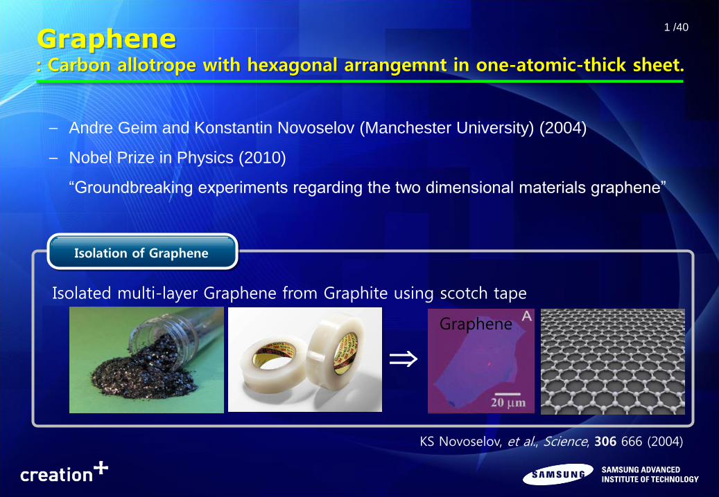
Graphene : Carbon allotrope with hexagonal arrangemnt in one-atomic-thick sheet.
KS Novoselov, et al., Science, 306 666 (2004)
Isolated multi-layer Graphene from Graphite using scotch tape
Isolation of Graphene
Graphene
– Andre Geim and Konstantin Novoselov (Manchester University) (2004)
– Nobel Prize in Physics (2010)
“Groundbreaking experiments regarding the two dimensional materials graphene”
Samsung Confidential
2 /40
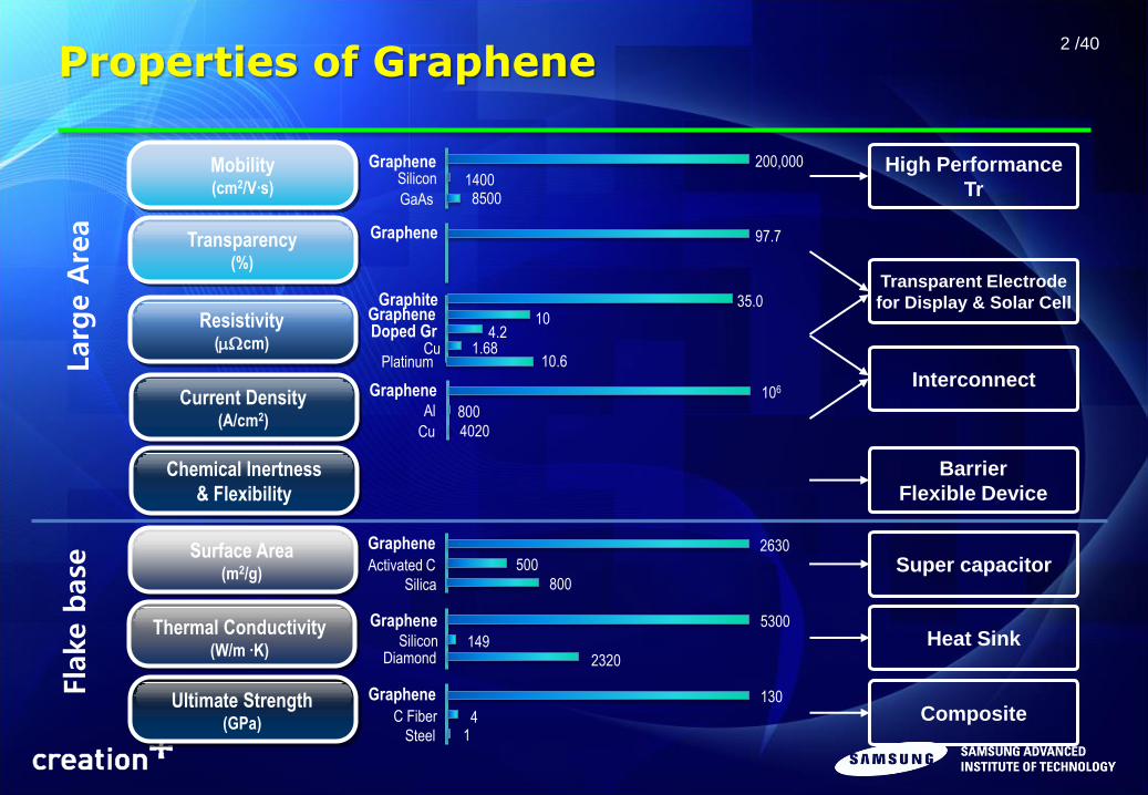
Properties of Graphene
Mobility (cm2/V∙s)
Graphene Silicon
GaAs
200,000 1400 8500
Graphene
C Fiber
Steel
130
4 1
Graphene Silicon
Diamond
5300
149 2320
Ultimate Strength (GPa)
Graphene
Activated C
Silica
2630
500
800
Surface Area (m2/g)
Graphene 97.7 Transparency (%)
Graphite
Cu Platinum
35.0
1.68 10.6
Resistivity (cm)
Thermal Conductivity (W/m ∙K)
4.2 Doped Gr
Graphene Al
Cu
106
800
4020
Current Density (A/cm2)
Graphene 10
High Performance
Tr
Transparent Electrode
for Display & Solar Cell
Super capacitor
Composite
Heat Sink
Interconnect
Larg
e A
rea
Fla
ke b
ase
Chemical Inertness
& Flexibility
Barrier
Flexible Device
Samsung Confidential
3 /40
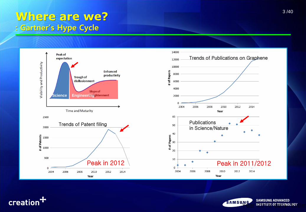
Where are we? : Gartner’s Hype Cycle
Year 2015 data: Estimation
Trends of Publications on Graphene
Publications in Science/Nature
Peak in 2011/2012 Peak in 2012
Trends of Patent filing
Science Engineering
Samsung Confidential
4 /40
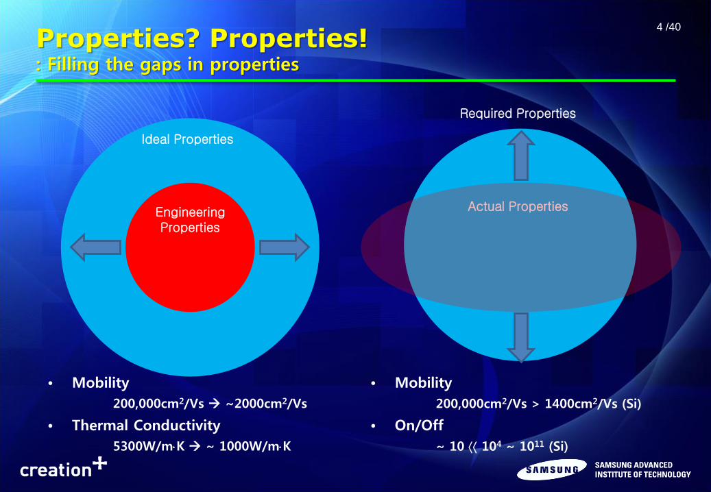
Properties? Properties! : Filling the gaps in properties
Ideal Properties
Engineering Properties
Actual Properties
Required Properties
• Mobility
200,000cm2/Vs ~2000cm2/Vs
• Thermal Conductivity
5300W/mK ~ 1000W/mK
• Mobility
200,000cm2/Vs > 1400cm2/Vs (Si)
• On/Off
~ 10 104 ~ 1011 (Si)
Samsung Confidential
5 /40
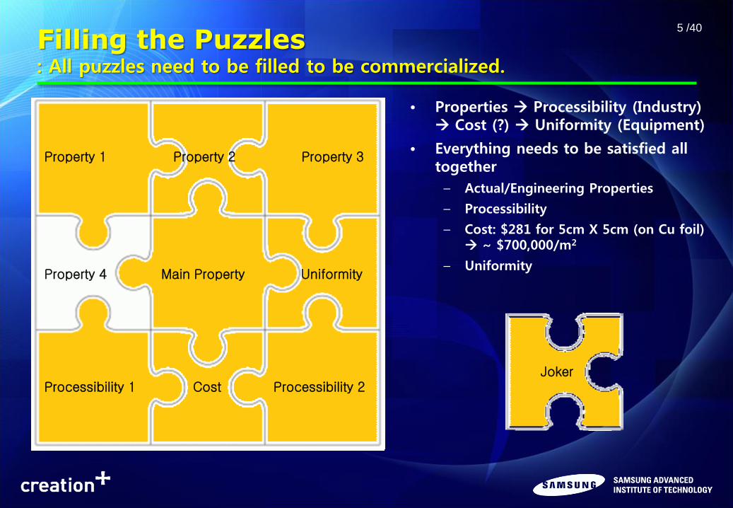
Filling the Puzzles : All puzzles need to be filled to be commercialized.
Property 1 Property 2 Property 3
Main Property
Processibility 1 Processibility 2 Cost
Property 4 Uniformity
• Properties Processibility (Industry) Cost (?) Uniformity (Equipment)
• Everything needs to be satisfied all together
– Actual/Engineering Properties
– Processibility
– Cost: $281 for 5cm X 5cm (on Cu foil) ~ $700,000/m2
– Uniformity
Joker
Samsung Confidential
6 /40
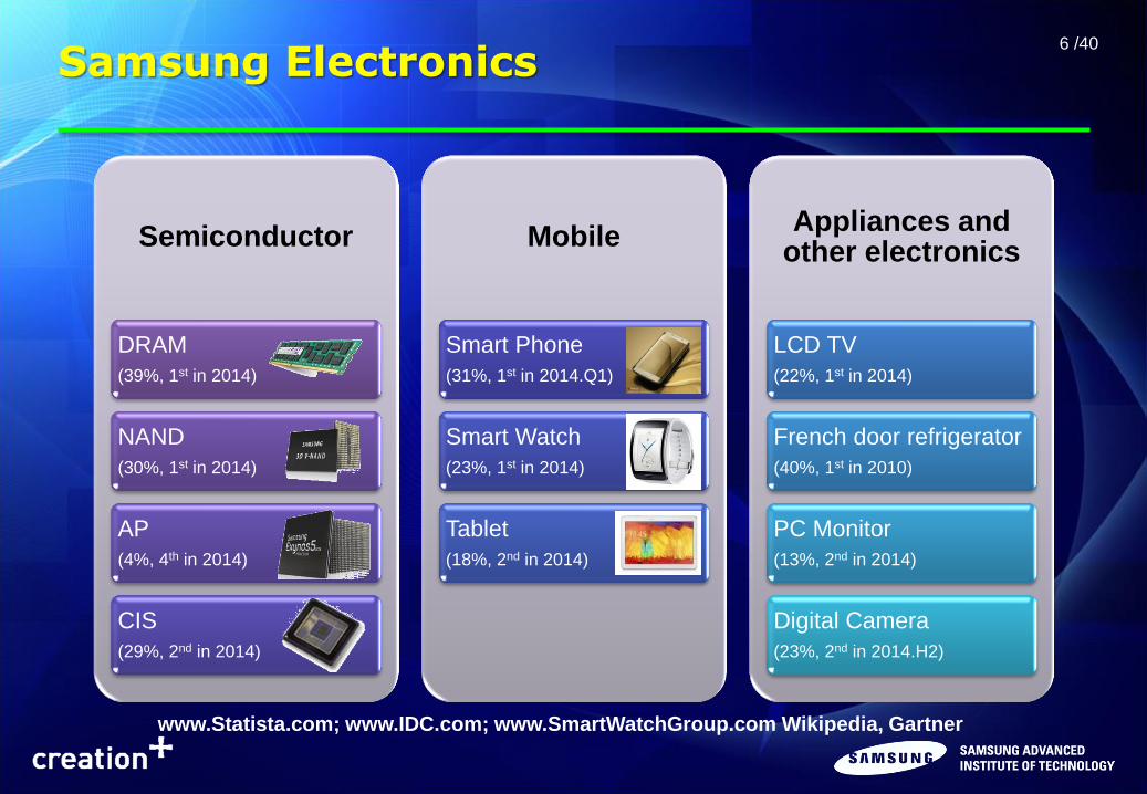
Samsung Electronics
www.Statista.com; www.IDC.com; www.SmartWatchGroup.com Wikipedia, Gartner
Semiconductor
DRAM
(39%, 1st in 2014)
NAND
(30%, 1st in 2014)
AP
(4%, 4th in 2014)
CIS
(29%, 2nd in 2014)
Mobile
Smart Phone
(31%, 1st in 2014.Q1)
Smart Watch
(23%, 1st in 2014)
Tablet
(18%, 2nd in 2014)
Appliances and other electronics
LCD TV
(22%, 1st in 2014)
French door refrigerator
(40%, 1st in 2010)
PC Monitor
(13%, 2nd in 2014)
Digital Camera
(23%, 2nd in 2014.H2)
Samsung Confidential
7 /40
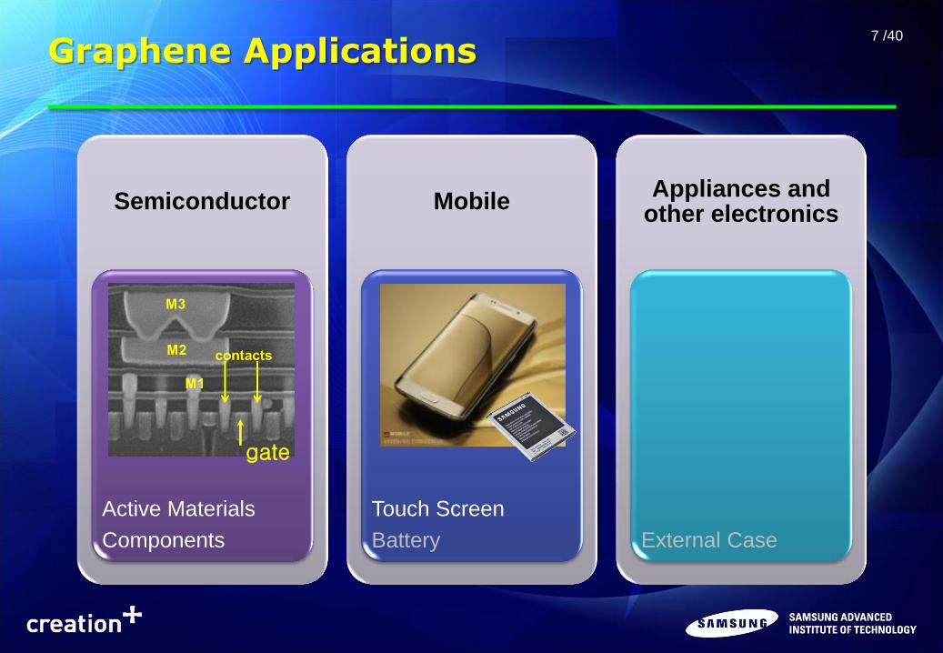
Graphene Applications
Semiconductor
Active Materials
Components
Mobile
Touch Screen
Battery
Appliances and other electronics
External Case
gate

Samsung Confidential
Growth
Samsung Confidential
9 /40
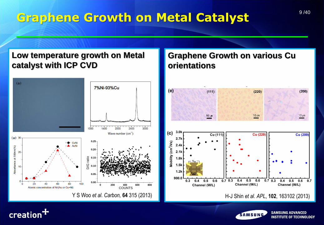
Graphene Growth on Metal Catalyst
Graphene Growth on various Cu
orientations
Low temperature growth on Metal
catalyst with ICP CVD
0 200 400 600 8000.00
0.05
0.10
0.15
0.20
0.25
D/G
ra
tio
COUNTS
Y S Woo et al. Carbon, 64 315 (2013) H-J Shin et al. APL, 102, 163102 (2013)
Samsung Confidential
10 /40
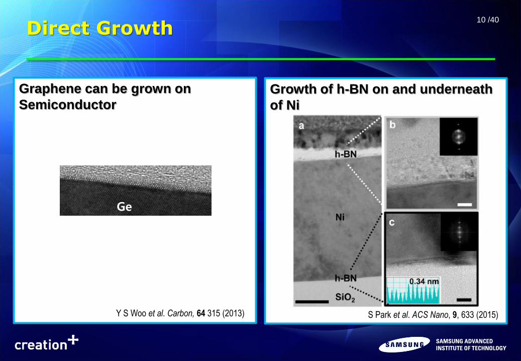
Direct Growth
Growth of h-BN on and underneath
of Ni
Graphene can be grown on
Semiconductor
Y S Woo et al. Carbon, 64 315 (2013) S Park et al. ACS Nano, 9, 633 (2015)
Ge
Samsung Confidential
Wafer-scale Integration of
Graphene Tunneling Barristor
Samsung Confidential
12 /40
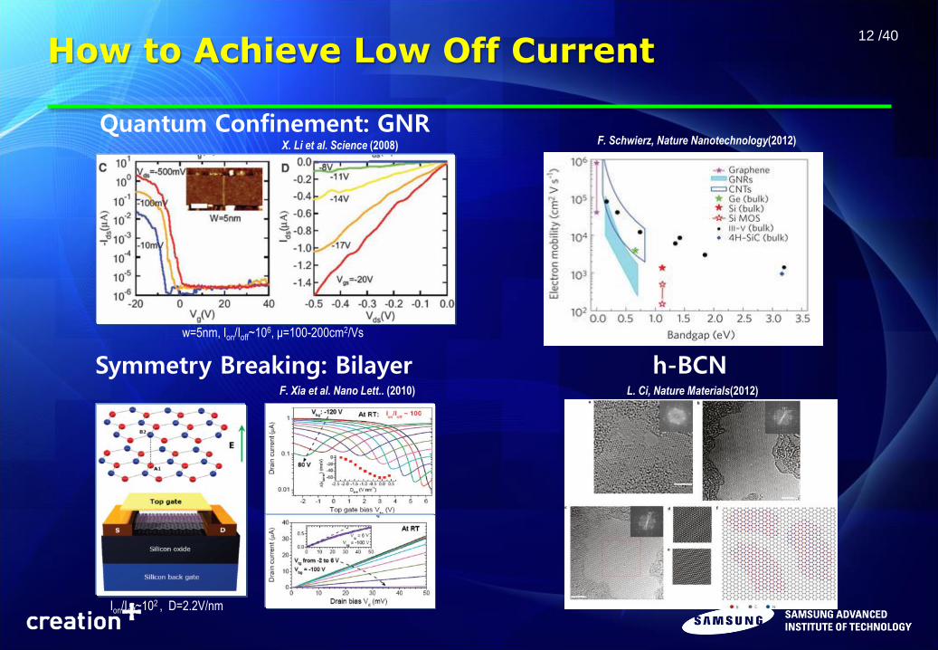
How to Achieve Low Off Current
Ion/Ioff~102 , D=2.2V/nm
X. Li et al. Science (2008)
F. Xia et al. Nano Lett.. (2010)
w=5nm, Ion/Ioff~106, μ=100-200cm2/Vs
F. Schwierz, Nature Nanotechnology(2012)
L. Ci, Nature Materials(2012)
Quantum Confinement: GNR
Symmetry Breaking: Bilayer h-BCN
Samsung Confidential
13 /40
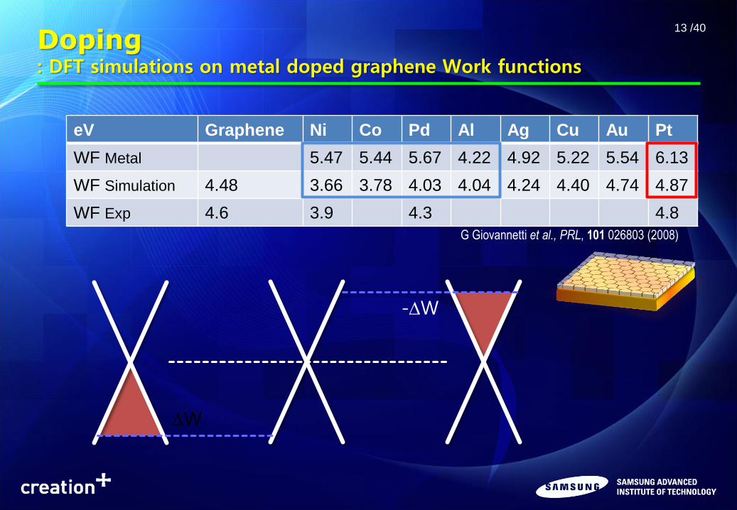
Doping : DFT simulations on metal doped graphene Work functions
eV Graphene Ni Co Pd Al Ag Cu Au Pt
WF Metal 5.47 5.44 5.67 4.22 4.92 5.22 5.54 6.13
WF Simulation 4.48 3.66 3.78 4.03 4.04 4.24 4.40 4.74 4.87
WF Exp 4.6 3.9 4.3 4.8
-W
W
G Giovannetti et al., PRL, 101 026803 (2008)
Samsung Confidential
14 /40
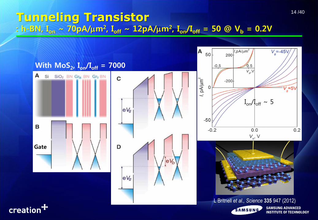
Tunneling Transistor : h-BN, Ion ~ 70pA/m2, Ioff ~ 12pA/m2, Ion/Ioff = 50 @ Vb = 0.2V
L Britnell et al., Science 335 947 (2012)
Gate
Ion/Ioff ~ 5
With MoS2, Ion/Ioff = 7000
Samsung Confidential
15 /40
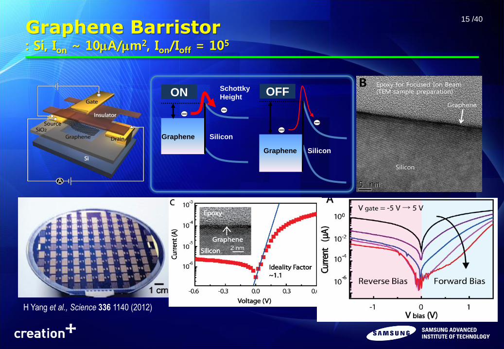
Graphene Barristor : Si, Ion ~ 10A/m2, Ion/Ioff = 105
Epoxy for Focused Ion Beam(TEM sample preparation)
Silicon Silicon
Epoxy for Focused Ion Beam(TEM sample preparation)
A B
Graphene
Graphene
Graphene Silicon
Graphene Silicon
Schottky
Height ON OFF
H Yang et al., Science 336 1140 (2012)
Samsung Confidential
16 /40
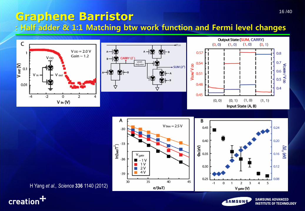
Graphene Barristor : Half adder & 1:1 Matching btw work function and Fermi level changes
H Yang et al., Science 336 1140 (2012)
Samsung Confidential
17 /40
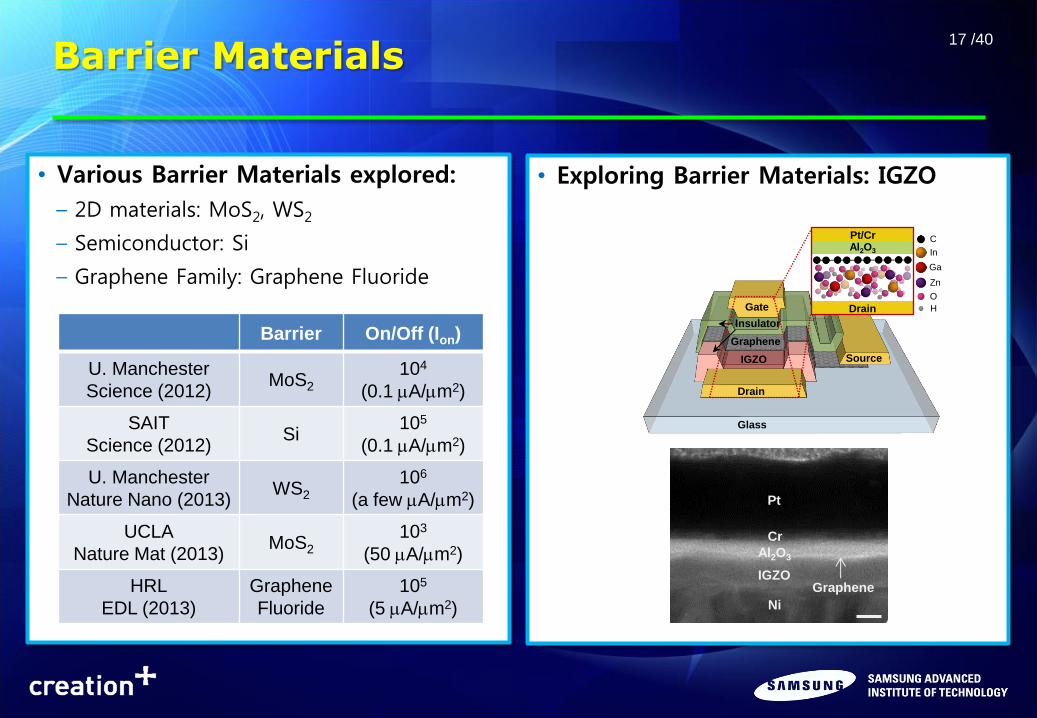
Barrier Materials
• Exploring Barrier Materials: IGZO • Various Barrier Materials explored:
– 2D materials: MoS2, WS2
– Semiconductor: Si
– Graphene Family: Graphene Fluoride
Barrier On/Off (Ion)
U. Manchester
Science (2012) MoS2
104
(0.1 A/m2)
SAIT
Science (2012) Si
105
(0.1 A/m2)
U. Manchester
Nature Nano (2013) WS2
106
(a few A/m2)
UCLA
Nature Mat (2013) MoS2
103
(50 A/m2)
HRL
EDL (2013)
Graphene
Fluoride
105
(5 A/m2)
Drain
Source IGZO
Gate
Graphene
Insulator
Pt/Cr
Drain
Al2O3
C
In
Ga
Zn
O
H
Glass
Ni
IGZO Graphene
Al2O3
Pt
Cr
Samsung Confidential
18 /40
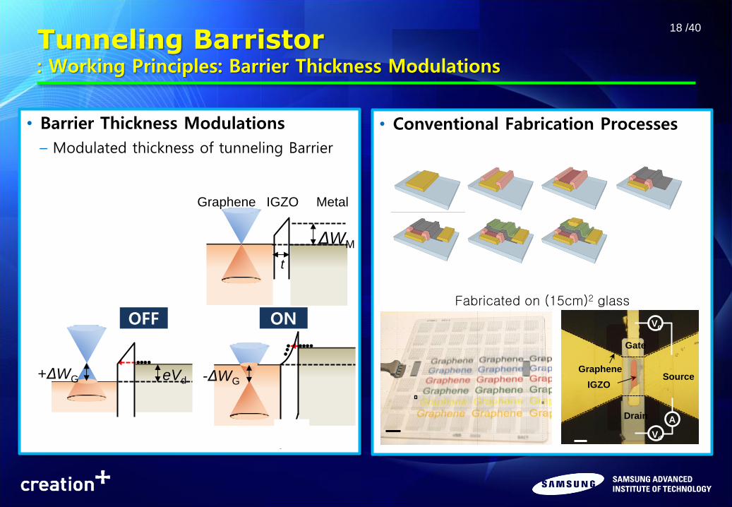
Tunneling Barristor : Working Principles: Barrier Thickness Modulations
• Conventional Fabrication Processes • Barrier Thickness Modulations
– Modulated thickness of tunneling Barrier
SEM Graphene
IGZO Source
Drain
Gate
A
Vg
Vd
Fabricated on (15cm)2 glass
-ΔWG
ΔWM
t
Graphene IGZO Metal
eVd +ΔWG
OFF ON
Samsung Confidential
19 /40
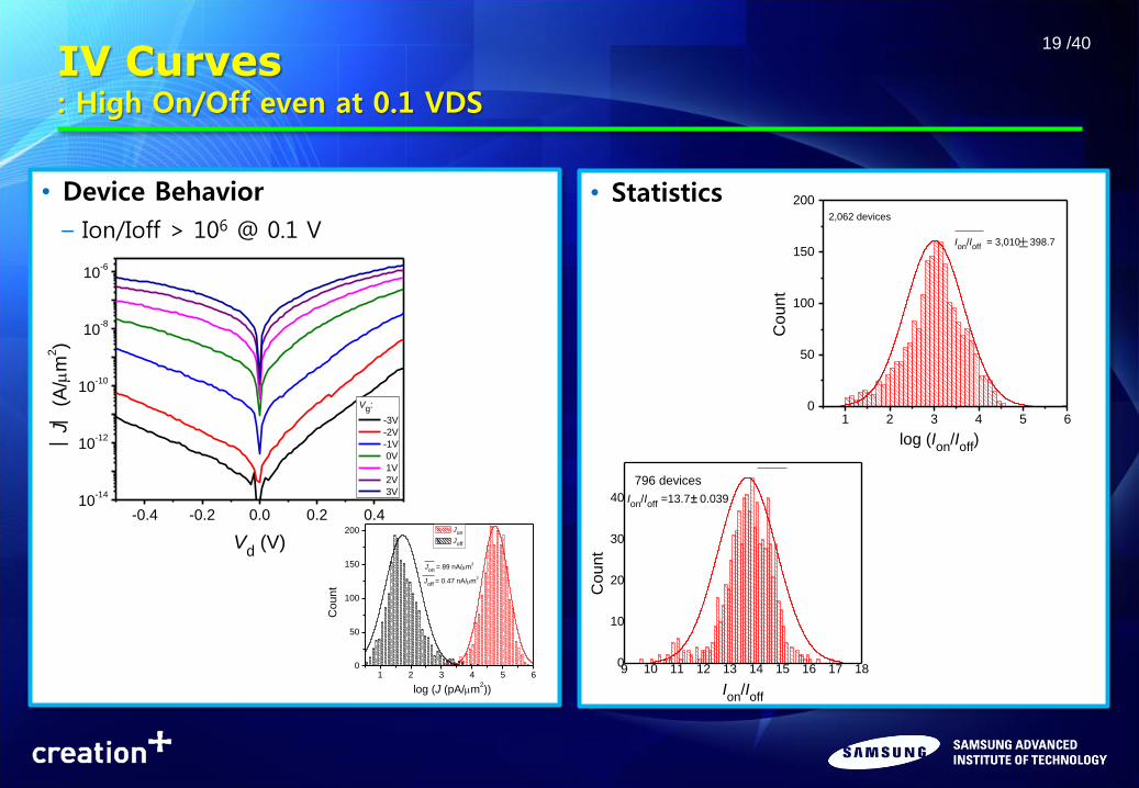
IV Curves : High On/Off even at 0.1 VDS
• Statistics • Device Behavior
– Ion/Ioff > 106 @ 0.1 V
±
±
-0.4 -0.2 0.0 0.2 0.410
-14
10-12
10-10
10-8
10-6
J
(
A/
m2)
Vd (V)
Vg:
-3V
-2V
-1V
0V
1V
2V
3V
0
2
4
6
8
10
1 2 3 4 5 60
50
100
150
200
Joff
= 0.47 nA/m2
Co
un
t
Jon
Joff
log (J (pA/m2))
Jon
= 89 nA/m2
1 2 3 4 5 60
50
100
150
200
Co
un
t
2,062 devices
log (Ion
/Ioff
)
Ion
/Ioff
= 3,010 398.7
9 10 11 12 13 14 15 16 17 180
10
20
30
40
Co
un
t
Ion
/Ioff
Ion
/Ioff
=13.7 0.039
796 devices
Samsung Confidential
20 /40
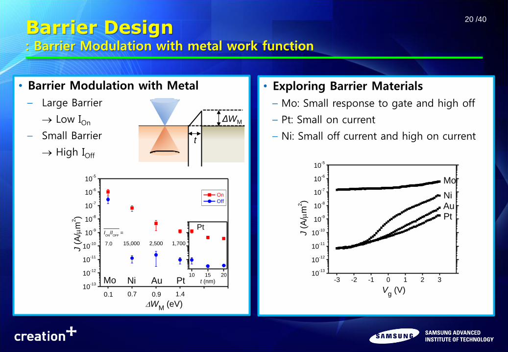
Barrier Design : Barrier Modulation with metal work function
• Exploring Barrier Materials
– Mo: Small response to gate and high off
– Pt: Small on current
– Ni: Small off current and high on current
• Barrier Modulation with Metal
– Large Barrier
Low IOn
– Small Barrier
High IOff
ΔWM
t
10-13
10-12
10-11
10-10
10-9
10-8
10-7
10-6
10-5
1.40.90.7
On
Off
J (
A/
m2)
WM
(eV)
7.0 15,000 2,500 1,700
0.1
ION
/IOFF
=
10 15 20
t (nm)Mo Ni Au Pt
Pt
-3 -2 -1 0 1 2 310
-13
10-12
10-11
10-10
10-9
10-8
10-7
10-6
10-5
Vg (V)
J (
A/
m2)
Mo
Ni Au Pt
Samsung Confidential
21 /40
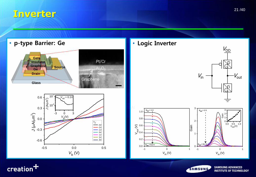
Inverter
• Logic Inverter • p-type Barrier: Ge
Graphene
Ge Al2O3
Pt/Cr
Drain
Source Ge
Gate
Graphene
Insulator
Glass
-3 0 3
10-8
10-7
J (
A/
m2)
Vg(V)
Vsd
= 0.1V
-0.5 0.0 0.5
-0.6
-0.3
0.0
0.3
0.6
Vg:
-3V
-2V
-1V
0V
1V
2V
3V
J (
A
/m
2)
Vb (V)
VDD
Vout Vin
G
G
p
n
Al
-1 0 1
0.0
0.2
0.4
0.6
0.8
1.0
VDD
= 0.1 V
Vo
ut (V
)
Vin
(V)
VDD
= 1 V
-1 0 1
0
1
2
3
Gain
Vin
(V)
VDD
= 1 V
VDD
= 0.1 V
0.0 0.5 1.0
0
1
2
3
Ga
in
VDD
(V)
Samsung Confidential
ALD on Graphene
23 /40
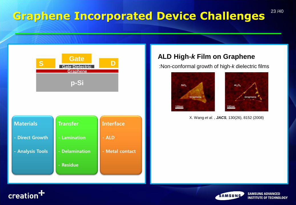
Graphene Incorporated Device Challenges
ALD High-k Film on Graphene
X. Wang et al. , JACS, 130(26), 8152 (2008)
:Non-conformal growth of high-k dielectric films Gate Dielectric
Gate
p-Si
S D Graphene
Materials
- Direct Growth
- Analysis Tools
Transfer
- Lamination
- Delamination
- Residue
Interface
- ALD
- Metal contact
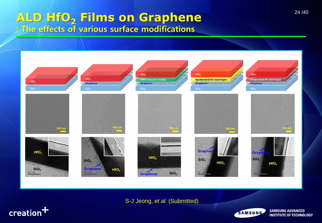
24 /40
ALD HfO2 Films on Graphene : The effects of various surface modifications
S-J Jeong, et al. (Submitted)
25 /40
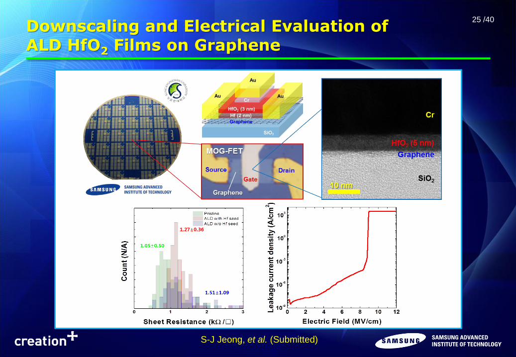
Downscaling and Electrical Evaluation of ALD HfO2 Films on Graphene
S-J Jeong, et al. (Submitted)
26 /40
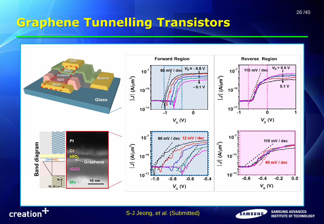
Graphene Tunnelling Transistors
S-J Jeong, et al. (Submitted)
27 /40
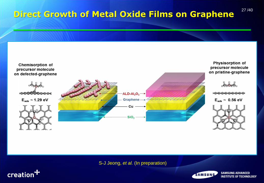
Direct Growth of Metal Oxide Films on Graphene
S-J Jeong, et al. (In preparation)
28 /40
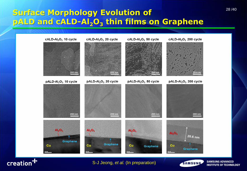
Surface Morphology Evolution of pALD and cALD-Al2O3 thin films on Graphene
S-J Jeong, et al. (In preparation)
29 /40
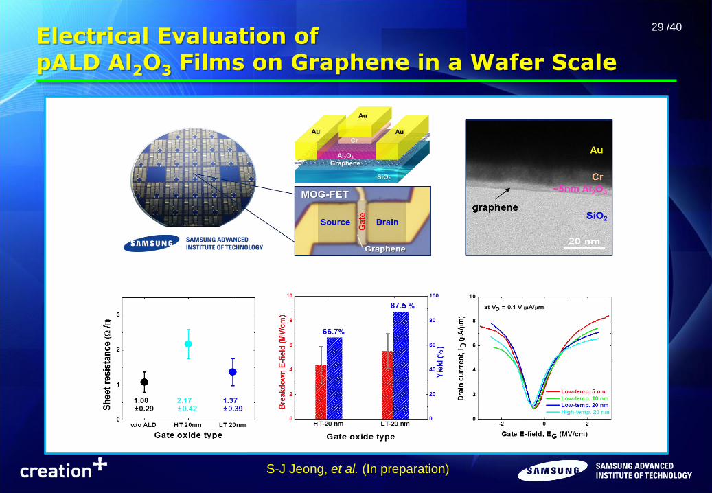
Electrical Evaluation of pALD Al2O3 Films on Graphene in a Wafer Scale
S-J Jeong, et al. (In preparation)
Samsung Confidential
Organic Light Emitting Transistor
31 /40
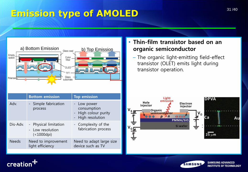
Emission type of AMOLED
• Thin-film transistor based on an organic semiconductor
– The organic light-emitting field-effect transistor (OLET) emits light during transistor operation.
– Line emission at recombined area
Bottom emission Top emission
Adv. - Simple fabrication process
- Low power consumption
- High colour purity - High resolution
Dis-Adv. - Physical limitation
- Low resolution (<1000dpi)
- Complexity of the fabrication process
Needs Need to improvement light efficiency
Need to adapt large size device such as TV
a) Bottom Emission b) Top Emission
32 /40
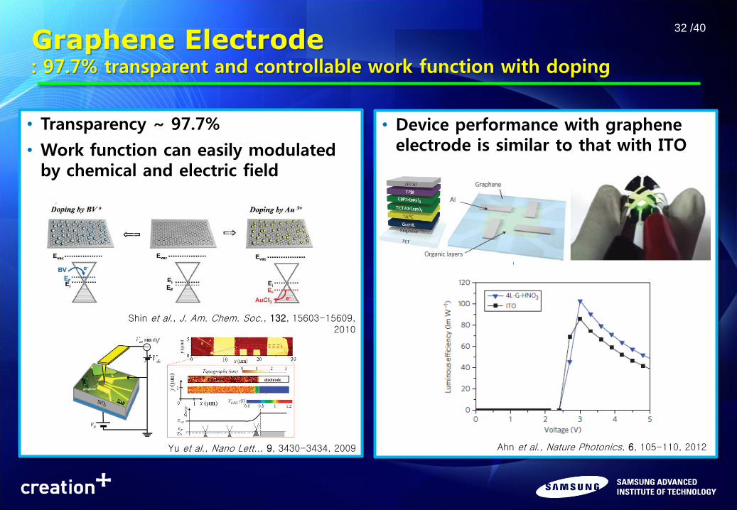
Graphene Electrode : 97.7% transparent and controllable work function with doping
• Device performance with graphene electrode is similar to that with ITO
• Transparency ~ 97.7%
• Work function can easily modulated by chemical and electric field
Shin et al., J. Am. Chem. Soc., 132, 15603-15609, 2010
Yu et al., Nano Lett.., 9, 3430-3434, 2009 Ahn et al., Nature Photonics, 6, 105-110, 2012
33 /40
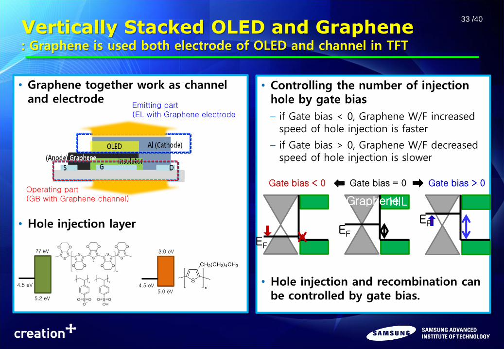
Vertically Stacked OLED and Graphene : Graphene is used both electrode of OLED and channel in TFT
• Controlling the number of injection hole by gate bias
– if Gate bias < 0, Graphene W/F increased speed of hole injection is faster
– if Gate bias > 0, Graphene W/F decreased speed of hole injection is slower
• Hole injection and recombination can be controlled by gate bias.
• Graphene together work as channel and electrode
• Hole injection layer
5.2 eV
?? eV
4.5 eV 5.0 eV
3.0 eV
4.5 eV
Operating part (GB with Graphene channel)
Emitting part (EL with Graphene electrode
Graphene HIL
EF EF
EF
Gate bias < 0 Gate bias = 0 Gate bias > 0
34 /40
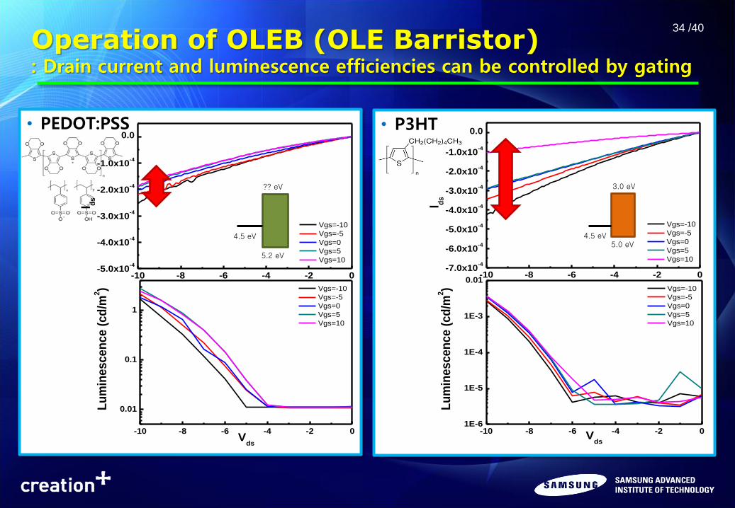
Operation of OLEB (OLE Barristor) : Drain current and luminescence efficiencies can be controlled by gating
• P3HT
• PEDOT:PSS
-10 -8 -6 -4 -2 0-5.0x10
-4
-4.0x10⁻⁴
-3.0x10⁻⁴
-2.0x10⁻⁴
-1.0x10⁻⁴
0.0
Vgs=-10
Vgs=-5
Vgs=0
Vgs=5
Vgs=10
I ds
-10 -8 -6 -4 -2 0
0.01
0.1
1
Vgs=-10
Vgs=-5
Vgs=0
Vgs=5
Vgs=10
Lu
min
esce
nce (
cd
/m2)
Vds
-10 -8 -6 -4 -2 0-7.0x10
-4
-6.0x10⁻⁴
-5.0x10⁻⁴
-4.0x10⁻⁴
-3.0x10⁻⁴
-2.0x10⁻⁴
-1.0x10⁻⁴
0.0
Vgs=-10
Vgs=-5
Vgs=0
Vgs=5
Vgs=10
I ds
-10 -8 -6 -4 -2 01E-6
1E-5
1E-4
1E-3
0.01 Vgs=-10
Vgs=-5
Vgs=0
Vgs=5
Vgs=10
Lu
min
es
ce
nc
e (
cd
/m2)
Vds
5.2 eV
?? eV
4.5 eV 5.0 eV
3.0 eV
4.5 eV
Samsung Confidential
Graphene for Si True Ohmic Contact
36 /40
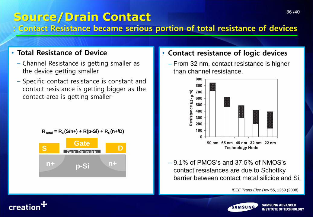
Source/Drain Contact : Contact Resistance became serious portion of total resistance of devices
• Contact resistance of logic devices
– From 32 nm, contact resistance is higher
than channel resistance.
– 9.1% of PMOS’s and 37.5% of NMOS’s
contact resistances are due to Schottky
barrier between contact metal silicide and Si.
• Total Resistance of Device
– Channel Resistance is getting smaller as the device getting smaller
– Specific contact resistance is constant and contact resistance is getting bigger as the contact area is getting smaller
Gate Dielectric
Gate
p-Si n+
S
n+
D
RTotal = RC(S/n+) + R(p-Si) + RC(n+/D)
IEEE Trans Elec Dev 55, 1259 (2008)
37 /40
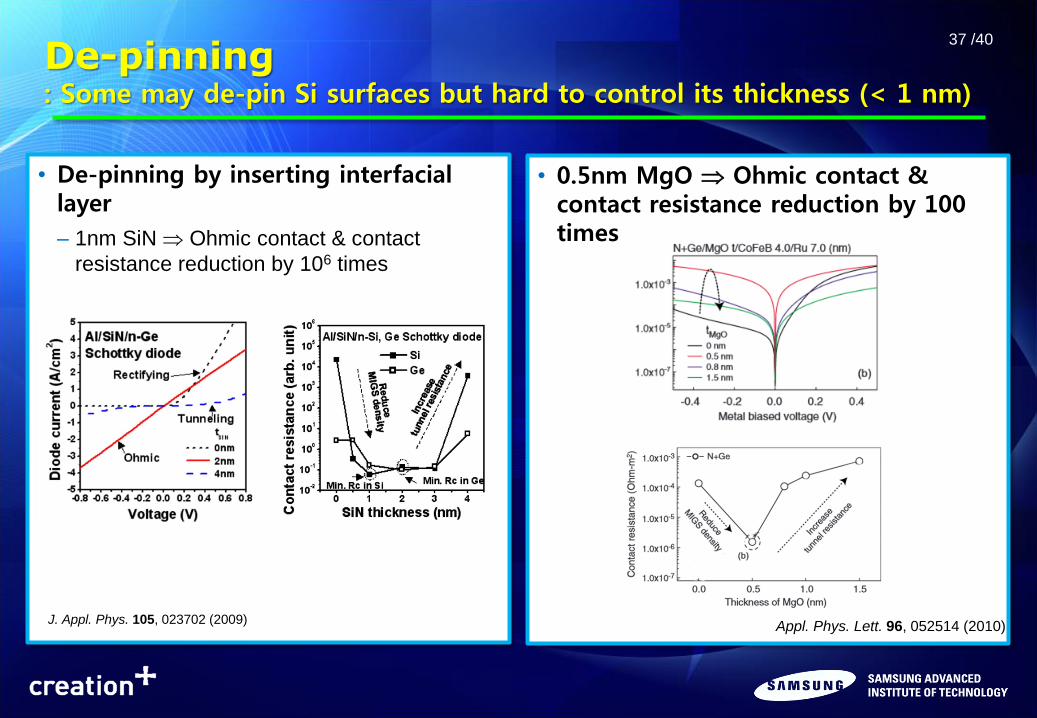
De-pinning : Some may de-pin Si surfaces but hard to control its thickness (< 1 nm)
• 0.5nm MgO Ohmic contact & contact resistance reduction by 100 times
• De-pinning by inserting interfacial layer
– 1nm SiN Ohmic contact & contact
resistance reduction by 106 times
J. Appl. Phys. 105, 023702 (2009) Appl. Phys. Lett. 96, 052514 (2010)
38 /40
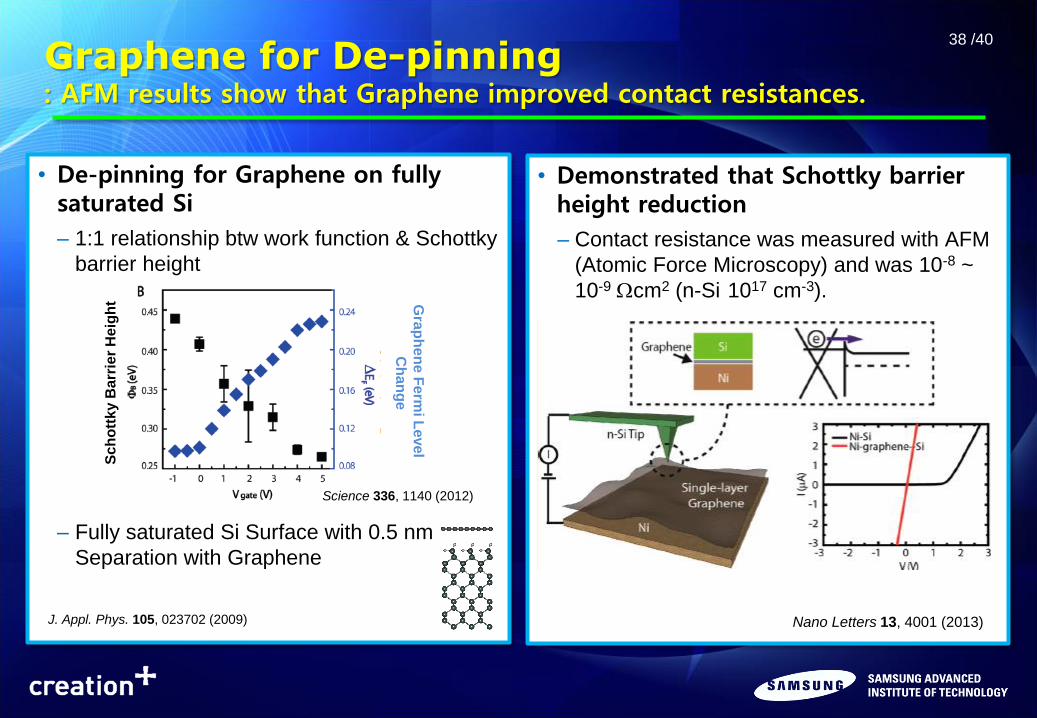
Graphene for De-pinning : AFM results show that Graphene improved contact resistances.
• Demonstrated that Schottky barrier height reduction
– Contact resistance was measured with AFM
(Atomic Force Microscopy) and was 10-8 ~
10-9 cm2 (n-Si 1017 cm-3).
• De-pinning for Graphene on fully saturated Si
– 1:1 relationship btw work function & Schottky
barrier height
– Fully saturated Si Surface with 0.5 nm
Separation with Graphene
J. Appl. Phys. 105, 023702 (2009)
Science 336, 1140 (2012)
Gra
ph
en
e F
erm
i Leve
l
Ch
an
ge
Sc
ho
ttk
y B
arr
ier
He
igh
t
Nano Letters 13, 4001 (2013)
39 /40
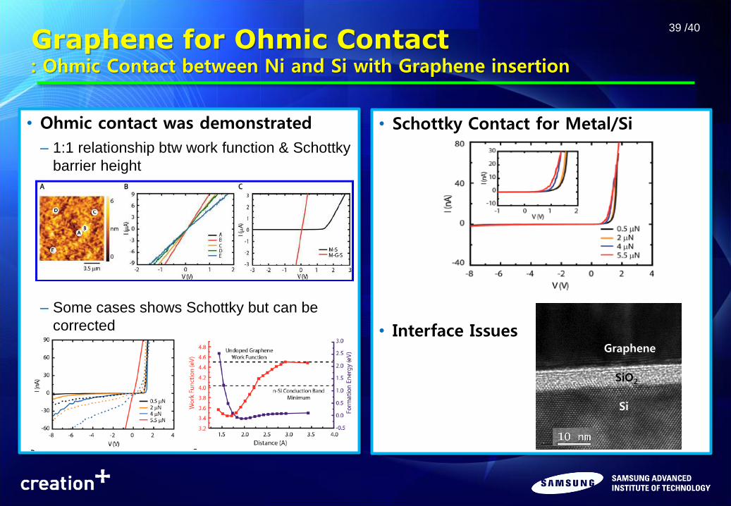
Graphene for Ohmic Contact : Ohmic Contact between Ni and Si with Graphene insertion
• Schottky Contact for Metal/Si
• Interface Issues
• Ohmic contact was demonstrated
– 1:1 relationship btw work function & Schottky
barrier height
– Some cases shows Schottky but can be
corrected
Science 336, 1140 (2012) Graphene
SiO2
Si
40 /40
Summary
• Graphene Propoerties
– High mobility, conductance, current density, transparency, chemical inertness
– Surface area, thermal conductivity, ultimate strength
• Applications
– New device concept: Gate-Tunable Schottky Diode / Barristor
– High current on-off ratio (>105) achieved
– OLET
– S/D Contacts
• Too early to say what will happen: The Long Game
– Nature, Editorials, May 2011
– It typically takes any technology some 20 years to emerge from the lab and be
commercialized.
Contact: [email protected]