Embed Size (px)
Citation preview
Graphene–assisted critically–coupledoptical ring modulator
Michele Midrio,1,∗ Stefano Boscolo,1 Michele Moresco,2
Marco Romagnoli,2 Costantino De Angelis,3 Andrea Locatelli,3
and Antonio-Daniele Capobianco4
1Dipartimento di Ingegneria Elettrica Gestionale e Meccanica,Universita degli Studi di Udine, 33100 Udine, Italy
2PhotonIC Corporation, 5800 Uplander Way, Los Angeles, CA 90230, USAMassachusetts Institute of Technology, 77 Massachusetts Ave, Cambridge, MA 02139, USA
3Dipartimento di Ingegneria dell’Informazione,Universita degli Studi di Brescia, 25123 Brescia, Italy
4Dipartimento di Ingegneria dell’Informazione,Universita degli Studi di Padova, 35131 Padova, Italy
Abstract: Graphene’s conductivity at optical frequencies can be variedupon injection of carriers. In the present paper, this effect is used tomodulate losses of an optical wave traveling inside a ring cavity. Thisway an optical modulator based on the critical–coupling concept firstintroduced by Yariv can be realized. Through numerical simulations, weshow that a modulator featuring a bandwidth as large as 100 GHz can bedesigned with switching energy in the order of few fJ per bit. Also, we showthat operations with driving voltages below 1.2 volt could be obtained,thus making the proposed modulator compatible with requirements oflow–voltage CMOS technology.
© 2012 Optical Society of America
OCIS codes: (250.4110) Modulators; (250.3140) Integrated optoelectronic circuits; (160.3130)Integrated optics materials; (060.4510) Optical communications.
References and links1. A. Yariv, “Critical coupling and its control in optical waveguide–ring resonator systems,” IEEE Photon. Technol.
Lett. 14, 483–485 (2002).2. R. A. Soref, and B. R. Bennett, “Kramers–Kronig analysis of electro–optical switching in silicon,” Proc. SPIE
704, 32–37 (1987).3. J. P. Lorenzo and R. A. Soref, “1.3 μm electro–optic silicon switch,” J. Appl. Phys. 51, 6–8 (1987).4. L. Friedman, R. A. Soref, and J. P. Lorenzo, “Silicon double–injection electro–optic modulator with junction
gate control,” J. Appl. Phys. 63, 1831–1839 (1988).5. S. R. Giguere, L. Friedman, R. A. Soref, and J. P. Lorenzo, “Simulation studies of silicon electro–optic waveguide
devices,” J. Appl. Phys. 68, 4964–4970 (1990).6. G. V. Treyez, P. G. May, and J. M. Halbout, “Silicon optical modulators at 1.3 micrometer based on free–carrier
absorption,” IEEE Electron. Dev. Lett. 12, 276–278 (1991).7. G. V. Treyez, P. G. May, and J. M. Halbout, “Silicon Mach–Zehnder waveguide inteferometers based on the
plasma dispersion effect,” Appl. Phys. Lett. 59, 771–773 (1991).8. U. Fischer, B. Schuppert, and K. Petermann, “Integrated optical switches in silicon based on SiGe–waveguides,”
IEEE Photon. Technol. Lett. 5, 785–787 (1993).9. H. C. Huang and T. C. Lo, “Simulation and analysis of silicon electro–optic modulators utilizing the carrier–
dispersion effect and impact–ionization mechanism,” J. Appl. Phys. 74, 1521–1582 (1993).10. A. Cutolo, M. Iodice, P. Spirito, and L. Zeni, “Silicon electro–optic modulator based on a three-terminal device
integrated in a low–loss single–mode SOI waveguide,” J. Lightwave Technol. 15, 505–518 (1997).
#169817 - $15.00 USD Received 1 Jun 2012; revised 13 Jul 2012; accepted 6 Aug 2012; published 24 Sep 2012(C) 2012 OSA 8 October 2012 / Vol. 20, No. 21 / OPTICS EXPRESS 23144
11. A. Sciuto, S. Libertino, A. Alessandria, S. Coffa, and G. Coppola, “Design, fabrication and testing of an integratedSi–based light modulator,” J. Lightwave Technol. 21, 228–235 (2003).
12. C. A. Barrios, V. R. de Almeida, and M. Lipson, “Low–power–consumption short–length and high–modulation–depth silicon electrooptic modulator,” J. Lightwave Technol. 21, 1089–1098 (2003).
13. A. Liu, R. Jones, L. Liao, D. Samara–Rubio, D. Rubin, O. Cohen, R. Nicolaescu, and M. Paniccia, “A high–speedsilicon optical modulator based on a metal–oxide semiconductor capacitor,” Nature 427, 615–618 (2004).
14. A. Liu, L. Liao, D. Rubin, H. Nguyen, B. Ciftcioglu, Y. Chetrit, N. Izhaki, and M. Paniccia, “High–speed opticalmodulation based on carrier depletion in a silicon waveguide,” Opt. Express 15, 660–668 (2007).
15. Q. Xu, S. Manipatrumi, B. Schmidt, J. Shakya, and M. Lipson, “12.5 Gbit/s carrier–injection–based siliconmicroring silicon modulators,” Opt. Express 15, 430–436 (2007).
16. Q. Xu, D. Fattal, and R. G. Beausoleil, “Silicon microring resonators with 1.5-μm radius,” Opt. Express 16,4309–4315 (2008).
17. P. Dong, R. Shafiiha, S. Liao, H. Liang, N.-N. Feng, D. Feng, G. Li, X. Zheng, A. V. Krishnamoorthy, and M.Ashgari, “Wavelength-tunable silicon microring modulator,” Opt. Express 18, 10941–10946 (2010).
18. W. A. Zortman, M. R. Watts, D. C. Trotter, R. W. Young and A. L. Lentine, “Low-power high-speed silicon mi-crodisk modulators,” in Proc. Conference on Lasers and Electro-Optics/Quantum Electronics and Laser ScienceConference (CLEO/QELS) (San Jose, Calif., 2004), paper CThJ4.
19. M. R. Watts, D. C. Trotter, R. W. Young, and A. L. Lentine, “Ultralow power silicon microdisk modulators andswitches,” in Proc. of the 5th IEEE International Conference on Group IV Photonics (Cardiff, Wales, 2008).
20. M. Liu, X. Yin, E. Ulin-Avila, B. Geng, T. Zentgraf, L. Ju, F. Wang, and X. Zhang. “A graphene-based broadbandoptical modulator,” Nature 474, 64–67 (2011).
21. M. Liu, X. Yin, and X. Zhang, “Double–layer graphene optical modulator,” Nano Lett. 12, 1482–1485 (2012).22. A. K. Geim and K. S. Novoselov, “The rise of graphene,” Nat. Mater. 6, 183–191 (2007).23. T. Stauber, N. M. R. Peres, and A. K. Geim, “Optical conductivity of graphene in the visible region of the
spectrum,” Phys. Rev. B 78, 085432 (2008).24. A. Vakil and N. Engheta, “Transformation optics using graphene,” Science 332, 1291–1294 (2008).25. G. W. Hanson, “Dyadic Green’s function and guided surface waves for a surface conductivity model of graphene,”
J. Appl. Phys. 103, 064302 (2008).26. CST Microwave Studio 2012. Darmstadt, Germany.27. T. Barwicz and H. A. Haus, “Three-dimensional analysis of scattering losses due to sidewall roughness in mi-
crophotonic waveguides,” J. Lightwave Technol. 23, 2719–2732 (2005).28. K. K. Lee, D. R. Lim, L. C. Kimerling, J. Shin, and F. Cerrina, “Fabrication of ultralow-loss Si/SiO2 waveguides
by roughness reduction,” Opt. Lett. 23, 1888–1890 (2001).29. M. Moresco, M. Romagnoli, S. Boscolo, and M. Midrio, “Method for Characterization of Si waveguide propa-
gation loss,” submitted to Opt. Express (2012).30. A. A. Balandin, S. Ghosh, W. Bao, I. Calizo, D. Teweldebrhan, F. Miao, and C. N. Lau, “Superior thermal
conductivity of single-layer graphene,” Nano Lett. 8, 902–907 (2008).31. C. T. DeRose, M. R. Watts, D. C. Trotter, D. L. Luck, G. N. Nielson, and R. W. Young, “Silicon microring mod-
ulator with integrated heater and temperature sensor for thermal control,” in Lasers and Electro-Optics/QuantumElectronics and Laser Science Conference 2010, paper CThJ3.
1. Introduction
Optical modulators are key components for telecommunications and optical interconnections.They are among the first integrated optics devices that have been studied since the mid 1980s.
Earliest designs were based on ferroelectric materials or III-V compounds. However, thedominance of silicon as the semiconductor choice for electronics, and the need of integration ofoptical and electronic functionalities onto the same chip eventually shifted the research effortstowards structures based on silicon-on-insulator substrates. A list of contributions that coversome relevant steps toward the design of modern modulators can be found in refs. [1–14].
Most of the structures reported in the papers above essentially are straight waveguides in aMach–Zehnder configuration. The key physical mechanism they rely on is the plasma disper-sion effect: silicon losses are modified upon injection of free carriers. Through Kramers–Kronigrelations, the refractive index of the material is modified as well. This may be used to producea π–shift in one of the Mach-Zehnder arms, and finally obtain the desired intensity modulation.The major drawback of this scheme is in the relative large dimensions it requires. Indeed, asplasma–dispersion can only induce small variations of the refractive index, interaction lengthsin the range of hundreds of microns to millimeters are needed.
#169817 - $15.00 USD Received 1 Jun 2012; revised 13 Jul 2012; accepted 6 Aug 2012; published 24 Sep 2012(C) 2012 OSA 8 October 2012 / Vol. 20, No. 21 / OPTICS EXPRESS 23145
In an attempt to reduce dimensions, and therefore allow for greater integration, ring–modulators were successively proposed. Plasma dispersion effect still is the key physical mech-anism. However, light which travels inside a cavity may now experience the refractive indexchange for thousands of time. This way, even a very tiny variation of the propagation con-stant may shift the wavelength of resonance by an amount large enough to allow for efficientamplitude modulation.
Based on this idea, devices with footprints in the range of 10 squared microns have beendemonstrated [15–17]. Owing to these very small dimensions, these devices also proved tohave exceptional performance in terms of power consumption [18, 19]. The price to pay is thenarrow bandwidth that resonances can offer. These are often limited to few GHz, and this finallybrings to the need for stringent fabrication capabilities and thermal control.
More recently, a novel kind of modulator has appeared in the open literature [20, 21]. Itmight represent a real break-through in the integrated–optics scenario, as it differs from plasma–dispersion–effect modulators in two respects.
1. The first is the use of graphene, the single sheet of carbon atoms in an hexagonal latticethat, among many other exceptional properties, has a much higher electron mobility thansilicon [22].
2. The second is the operation principle it exploits. Indeed, this modulator directly relieson loss modulation rather than on loss-induced refractive index variations. The strikingpoint is that, essentially, this is “just” an electro–absorption modulator. As such, it mayoperate over a virtually endless optical band, but with much better performance than“conventional” electro–optic modulators in terms of electrical bandwidth.
Unfortunately, the differential loss that can be achieved by modulating graphene losses isrelatively small. Values in the range of 0.1÷0.15 dB/μm were demonstrated in refs. [20, 21].This in turn means that if an extinction ratio of 6÷10 dB is looked for between the “ON” and“OFF” states of the modulator, a device length in the order of 50÷100 μm must be foreseen.As we shall illustrate below this could lead to rather severe impairments in terms of switching–energy consumption.
At this stage, one might observe that it looks like the potential of graphene in the frameworkof optical modulation were following the same path as that of the plasma–dispersion–effect. In-deed, a promising technology has become available, but dimensions (and energy consumption)yet are the main limiting factors. Just in the same way as it was done with plasma–dispersion–effect modulators, one might therefore wonder whether inserting graphene into a resonant ringstructure could help to improve the performance or not. The aim of the present paper is that ofinvestigating the point, to quantify the bandwidth and energy consumption that can be foreseenwhen designing a graphene–assisted optical ring modulator.
2. Principle of operation
We exploit the physical effect introduced in 2002 by A. Yariv: the critical coupling [1] that canbe obtained in ring structure as the one sketched in the inset of Fig. 1.
For the sake of clarity we briefly review the main result of ref. [1], and we use the samesymbols as in the original paper. Letting t and α the single–pass transmission through thestraight waveguide, and through the ring, respectively, the scattering matrix of the coupler readsas [
b1
b2
]=
[t k∗−k t
][a1
a2
], with |t|2 + |k|2 = 1 and a2 = αb2eiϕ . (1)
#169817 - $15.00 USD Received 1 Jun 2012; revised 13 Jul 2012; accepted 6 Aug 2012; published 24 Sep 2012(C) 2012 OSA 8 October 2012 / Vol. 20, No. 21 / OPTICS EXPRESS 23146
� ��� ��� ��� ��� ���
��
�
���
�� ���������������α)
���
���
���
���
�
���
��
��
��
��
�����α������ϕ α = α����
�
������� �
��!" �� ���
ψ#��"$���
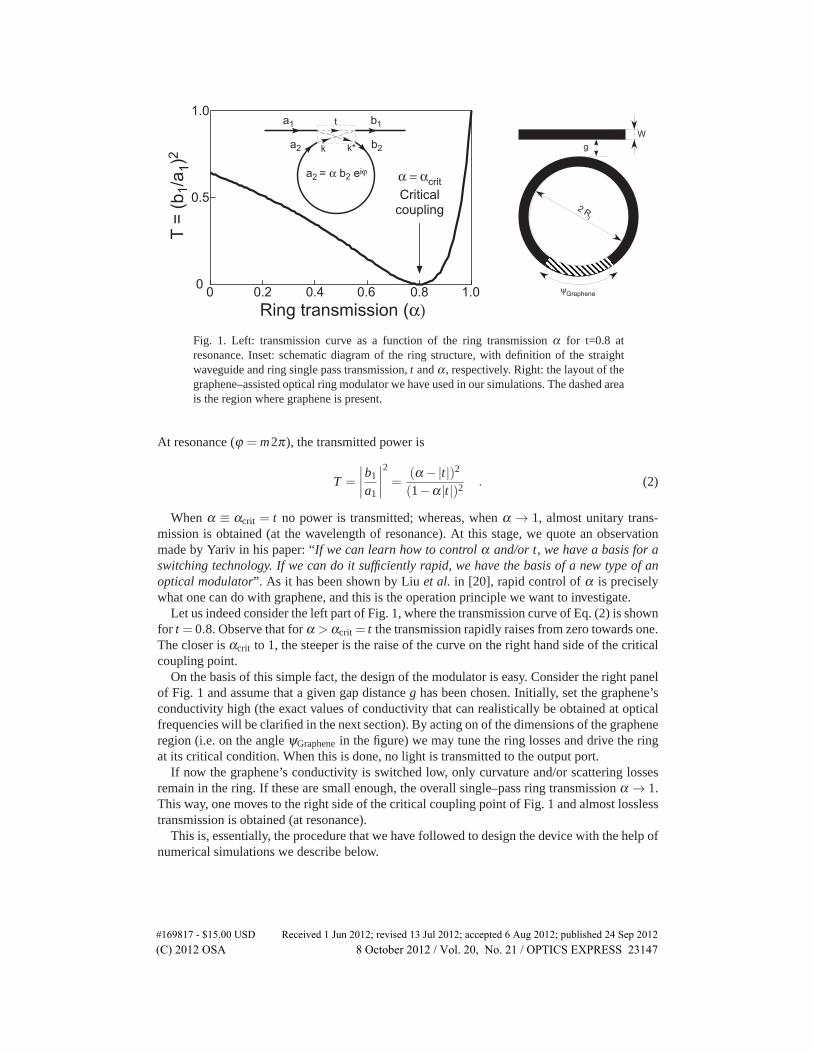
%
Fig. 1. Left: transmission curve as a function of the ring transmission α for t=0.8 atresonance. Inset: schematic diagram of the ring structure, with definition of the straightwaveguide and ring single pass transmission, t and α , respectively. Right: the layout of thegraphene–assisted optical ring modulator we have used in our simulations. The dashed areais the region where graphene is present.
At resonance (ϕ = m2π), the transmitted power is
T =
∣∣∣∣b1
a1
∣∣∣∣2
=(α −|t|)2
(1−α|t|)2 . (2)
When α ≡ αcrit = t no power is transmitted; whereas, when α → 1, almost unitary trans-mission is obtained (at the wavelength of resonance). At this stage, we quote an observationmade by Yariv in his paper: “If we can learn how to control α and/or t, we have a basis for aswitching technology. If we can do it sufficiently rapid, we have the basis of a new type of anoptical modulator”. As it has been shown by Liu et al. in [20], rapid control of α is preciselywhat one can do with graphene, and this is the operation principle we want to investigate.
Let us indeed consider the left part of Fig. 1, where the transmission curve of Eq. (2) is shownfor t = 0.8. Observe that for α > αcrit = t the transmission rapidly raises from zero towards one.The closer is αcrit to 1, the steeper is the raise of the curve on the right hand side of the criticalcoupling point.
On the basis of this simple fact, the design of the modulator is easy. Consider the right panelof Fig. 1 and assume that a given gap distance g has been chosen. Initially, set the graphene’sconductivity high (the exact values of conductivity that can realistically be obtained at opticalfrequencies will be clarified in the next section). By acting on of the dimensions of the grapheneregion (i.e. on the angle ψGraphene in the figure) we may tune the ring losses and drive the ringat its critical condition. When this is done, no light is transmitted to the output port.
If now the graphene’s conductivity is switched low, only curvature and/or scattering lossesremain in the ring. If these are small enough, the overall single–pass ring transmission α → 1.This way, one moves to the right side of the critical coupling point of Fig. 1 and almost losslesstransmission is obtained (at resonance).
This is, essentially, the procedure that we have followed to design the device with the help ofnumerical simulations we describe below.
#169817 - $15.00 USD Received 1 Jun 2012; revised 13 Jul 2012; accepted 6 Aug 2012; published 24 Sep 2012(C) 2012 OSA 8 October 2012 / Vol. 20, No. 21 / OPTICS EXPRESS 23147
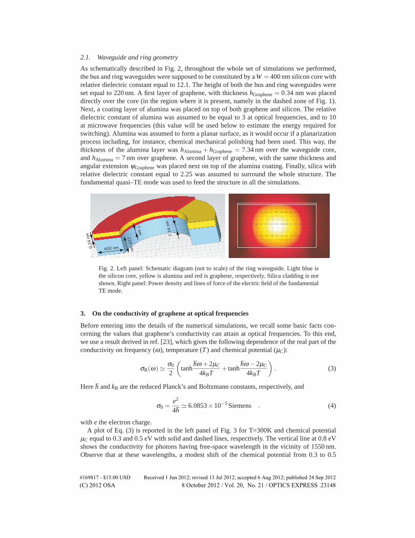
2.1. Waveguide and ring geometry
As schematically described in Fig. 2, throughout the whole set of simulations we performed,the bus and ring waveguides were supposed to be constituted by a W = 400 nm silicon core withrelative dielectric constant equal to 12.1. The height of both the bus and ring waveguides wereset equal to 220 nm. A first layer of graphene, with thickness hGraphene = 0.34 nm was placeddirectly over the core (in the region where it is present, namely in the dashed zone of Fig. 1).Next, a coating layer of alumina was placed on top of both graphene and silicon. The relativedielectric constant of alumina was assumed to be equal to 3 at optical frequencies, and to 10at microwave frequencies (this value will be used below to estimate the energy required forswitching). Alumina was assumed to form a planar surface, as it would occur if a planarizationprocess including, for instance, chemical mechanical polishing had been used. This way, thethickness of the alumina layer was hAlumina + hGraphene = 7.34 nm over the waveguide core,and hAlumina = 7 nm over graphene. A second layer of graphene, with the same thickness andangular extension ψGraphene was placed next on top of the alumina coating. Finally, silica withrelative dielectric constant equal to 2.25 was assumed to surround the whole structure. Thefundamental quasi–TE mode was used to feed the structure in all the simulations.
������
�����
���
���
�
��
�
�
���
�
Fig. 2. Left panel: Schematic diagram (not to scale) of the ring waveguide. Light blue isthe silicon core, yellow is alumina and red is graphene, respectively. Silica cladding is notshown. Right panel: Power density and lines of force of the electric field of the fundamentalTE mode.
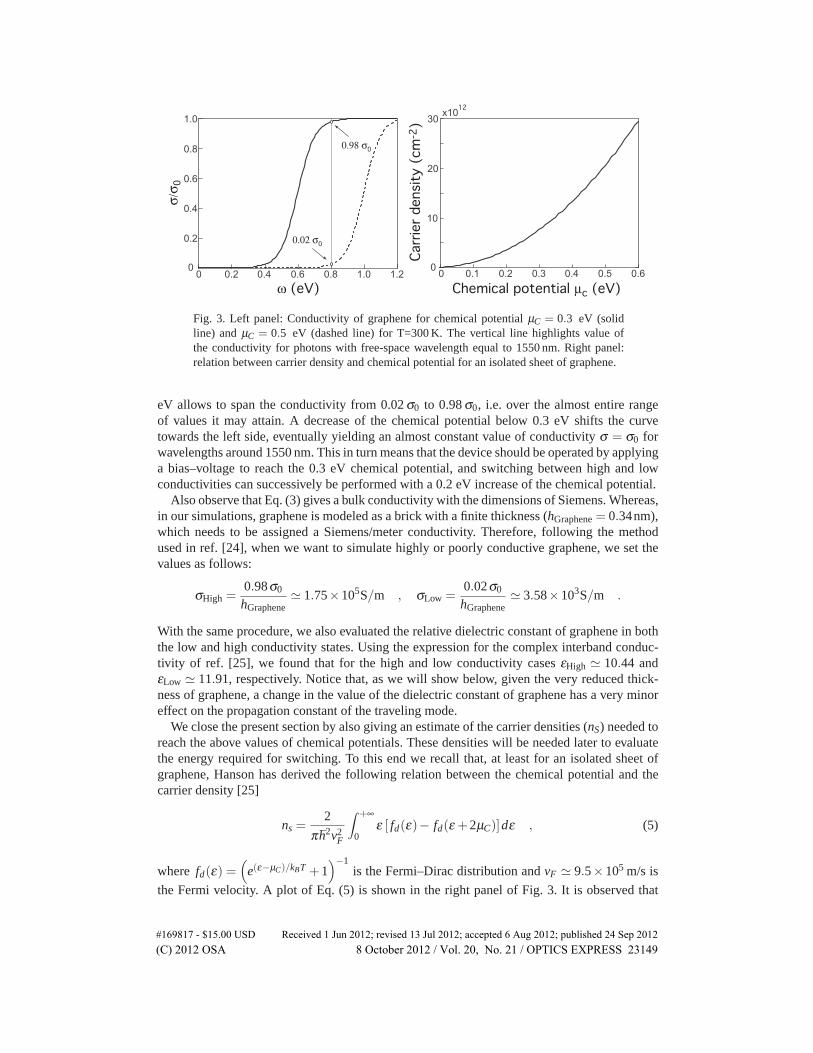
3. On the conductivity of graphene at optical frequencies
Before entering into the details of the numerical simulations, we recall some basic facts con-cerning the values that graphene’s conductivity can attain at optical frequencies. To this end,we use a result derived in ref. [23], which gives the following dependence of the real part of theconductivity on frequency (ω), temperature (T ) and chemical potential (μC):
σR(ω)� σ0
2
(tanh
hω +2μC
4kBT+ tanh
hω −2μC
4kBT
). (3)
Here h and kB are the reduced Planck’s and Boltzmann constants, respectively, and
σ0 =e2
4h� 6.0853×10⁻⁵ Siemens . (4)
with e the electron charge.A plot of Eq. (3) is reported in the left panel of Fig. 3 for T=300K and chemical potential
μC equal to 0.3 and 0.5 eV with solid and dashed lines, respectively. The vertical line at 0.8 eVshows the conductivity for photons having free-space wavelength in the vicinity of 1550 nm.Observe that at these wavelengths, a modest shift of the chemical potential from 0.3 to 0.5
#169817 - $15.00 USD Received 1 Jun 2012; revised 13 Jul 2012; accepted 6 Aug 2012; published 24 Sep 2012(C) 2012 OSA 8 October 2012 / Vol. 20, No. 21 / OPTICS EXPRESS 23148
���� ��� ��� ��� ��� ����
���
���
���
���
���
ω��� �
σ/σ �
0.98 σ�
0.02 σ�
��
���
���
&��
� ��� ��� ��& ��� �� ���
���������������������� �
������
���
��������
��
���
'�����
Fig. 3. Left panel: Conductivity of graphene for chemical potential μC = 0.3 eV (solidline) and μC = 0.5 eV (dashed line) for T=300 K. The vertical line highlights value ofthe conductivity for photons with free-space wavelength equal to 1550 nm. Right panel:relation between carrier density and chemical potential for an isolated sheet of graphene.
eV allows to span the conductivity from 0.02 σ0 to 0.98 σ0, i.e. over the almost entire rangeof values it may attain. A decrease of the chemical potential below 0.3 eV shifts the curvetowards the left side, eventually yielding an almost constant value of conductivity σ = σ0 forwavelengths around 1550 nm. This in turn means that the device should be operated by applyinga bias–voltage to reach the 0.3 eV chemical potential, and switching between high and lowconductivities can successively be performed with a 0.2 eV increase of the chemical potential.
Also observe that Eq. (3) gives a bulk conductivity with the dimensions of Siemens. Whereas,in our simulations, graphene is modeled as a brick with a finite thickness (hGraphene = 0.34nm),which needs to be assigned a Siemens/meter conductivity. Therefore, following the methodused in ref. [24], when we want to simulate highly or poorly conductive graphene, we set thevalues as follows:
σHigh =0.98σ0
hGraphene� 1.75×10⁵S/m , σLow =
0.02σ0
hGraphene� 3.58×10³S/m .
With the same procedure, we also evaluated the relative dielectric constant of graphene in boththe low and high conductivity states. Using the expression for the complex interband conduc-tivity of ref. [25], we found that for the high and low conductivity cases εHigh � 10.44 andεLow � 11.91, respectively. Notice that, as we will show below, given the very reduced thick-ness of graphene, a change in the value of the dielectric constant of graphene has a very minoreffect on the propagation constant of the traveling mode.
We close the present section by also giving an estimate of the carrier densities (nS) needed toreach the above values of chemical potentials. These densities will be needed later to evaluatethe energy required for switching. To this end we recall that, at least for an isolated sheet ofgraphene, Hanson has derived the following relation between the chemical potential and thecarrier density [25]
ns =2
π h2v2F
∫ +∞
0ε [ fd(ε)− fd(ε +2μC)]dε , (5)
where fd(ε) =(
e(ε−μC)/kBT +1)−1
is the Fermi–Dirac distribution and vF � 9.5× 10⁵ m/s is
the Fermi velocity. A plot of Eq. (5) is shown in the right panel of Fig. 3. It is observed that
#169817 - $15.00 USD Received 1 Jun 2012; revised 13 Jul 2012; accepted 6 Aug 2012; published 24 Sep 2012(C) 2012 OSA 8 October 2012 / Vol. 20, No. 21 / OPTICS EXPRESS 23149
chemical potentials equal to 0.3 and 0.5 eV can be obtained with carrier densities roughly equalto ρOFF = 7.5× 1012 cm−2 and ρON = 20.5× 1012 cm−2, respectively. Use of subscripts OFFand ON will become clear later on.
4. Numerical simulations and results
We refer again to the structure illustrated in the right panel of Fig. 1 above. All our simu-lations were performed with commercial codes CST [26] and COMSOL. Frequency–domainsimulations based on the finite–element method were performed with both the codes. CST wasused to perform all the simulations of propagation through the ring. Whereas, COMSOL wasused mainly to check the accuracy of the propagation constant and mode profile computed bythe modal analysis tool of CST. We underline that use of an accurate tetrahedral unstructuredmesh proved to be compulsory in order to get reliable results. This is consistent with resultsof ref. [27] where it was shown that even a 2 nm roughness in the waveguide sidewalls maygive rise to remarkable scattering losses. This in turn means that if we had used a structuredstaircase mesh, even with cell dimensions as small as 10 nm, a value which would have broughtto extreme large computational time and memory occupancy, the main numerical effect we hadobserved would have been that of an artificially big scattering loss.
A preliminary analysis was conducted to characterize the propagation constant of the modein the waveguide (a straight one), either in the absence or in the presence of graphene, both inthe high and low conductivity states.
It turned out that, for free space–wavelength λ0 � 1550nm, the mode has the followingeffective indices:
No graphene neff = 2.2576Graphene with low conductivity (σ = σLow, ε = εLow) neff = 2.2543− i8.42×10−5
Graphene with high conductivity (σ = σHigh, ε = εHigh) neff = 2.2546− i3.79×10−3
It is observed that graphene’s effect is mostly on the imaginary part of the effective index,i.e. on losses. Indeed the mode profiles in the three cases above were almost undistinguishable.This in turn means that no scattering from mode–mismatch is expected when the field crossesthe interfaces between the ring sections with and without graphene. Indeed, both because of itsextremely tiny thickness, and of relatively small conductivity, graphene acts as a sort of first–order perturbative term: mainly, it introduces an imaginary part in the propagation constantwithout altering the mode profile in a significant way.
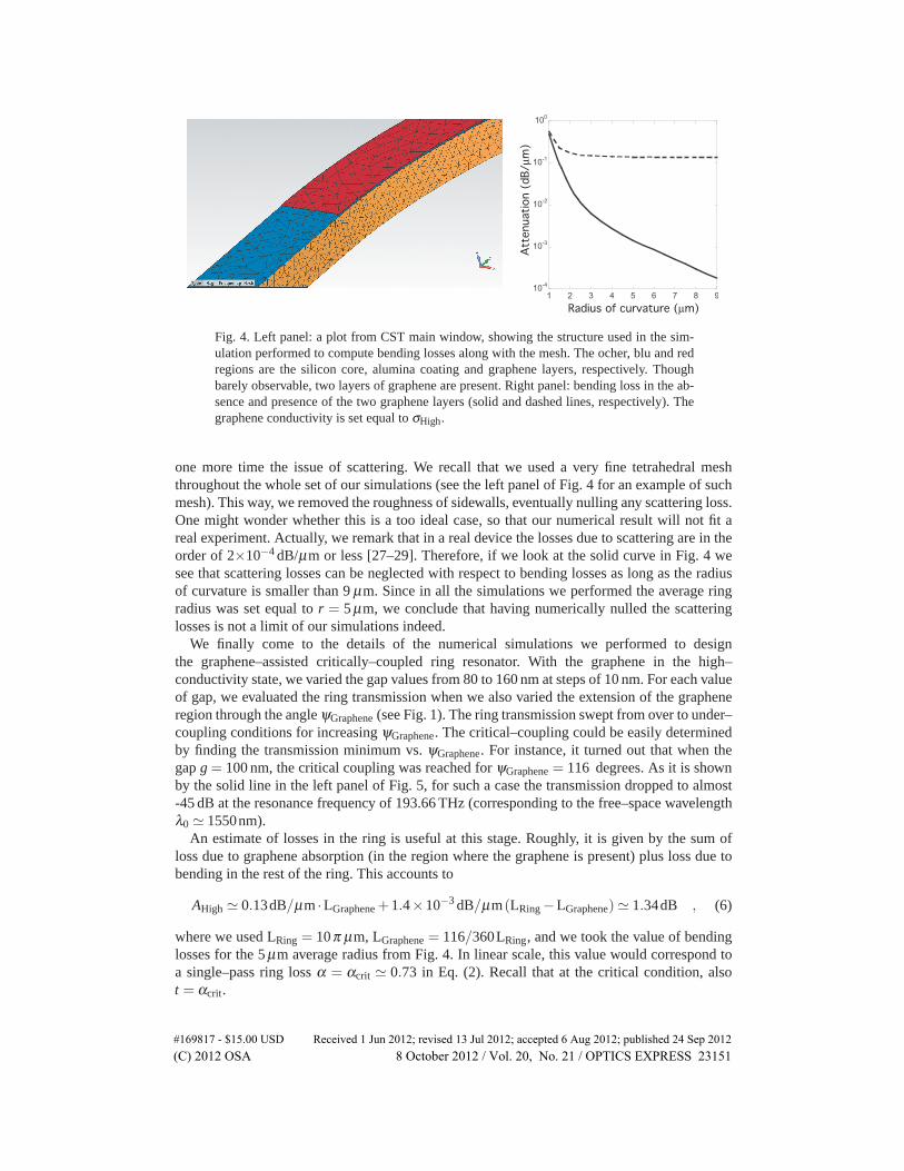
A second preliminary analysis was also conducted in order to evaluate the bending losses as afunction of radius of curvature. The results of this analysis are reported in Fig. 4 for rings in theabsence (solid line) and presence (dashed line) of graphene, respectively. In these simulations,the conductivity of graphene, when present, is set equal to σHigh. The abscissa in the figurehas to be intended as the average ring radius (i.e. the internal ring radius plus half the ringwaveguide width).
In the absence of graphene, the bending losses decrease towards zero for increasing radii, asexpected. Whereas, the behavior in the presence of graphene is more interesting. For large radii,the curve tends to a limiting value, in the order of 0.13 dB/μm. This value exactly correspondsto the loss of the mode in the straight waveguide we have discussed above, when we found theeffective index neff = 2.2546− i3.79×10−3. We conclude that the curvature loss is negligiblewith respect to graphene absorption for curvature radii greater than about 3 μm. For smallerradii, bending losses tend to become so large that they shadow graphene’s absorption.
Since the critical coupling is the key factor in the proposed device, and since this stronglydepends on ring losses, we conclude the presentation of these preliminary results by stressing
#169817 - $15.00 USD Received 1 Jun 2012; revised 13 Jul 2012; accepted 6 Aug 2012; published 24 Sep 2012(C) 2012 OSA 8 October 2012 / Vol. 20, No. 21 / OPTICS EXPRESS 23150
�������� ����!��������
"���������
���
�#$
�
Fig. 4. Left panel: a plot from CST main window, showing the structure used in the sim-ulation performed to compute bending losses along with the mesh. The ocher, blu and redregions are the silicon core, alumina coating and graphene layers, respectively. Thoughbarely observable, two layers of graphene are present. Right panel: bending loss in the ab-sence and presence of the two graphene layers (solid and dashed lines, respectively). Thegraphene conductivity is set equal to σHigh.
one more time the issue of scattering. We recall that we used a very fine tetrahedral meshthroughout the whole set of our simulations (see the left panel of Fig. 4 for an example of suchmesh). This way, we removed the roughness of sidewalls, eventually nulling any scattering loss.One might wonder whether this is a too ideal case, so that our numerical result will not fit areal experiment. Actually, we remark that in a real device the losses due to scattering are in theorder of 2×10⁻⁴ dB/μm or less [27–29]. Therefore, if we look at the solid curve in Fig. 4 wesee that scattering losses can be neglected with respect to bending losses as long as the radiusof curvature is smaller than 9 μm. Since in all the simulations we performed the average ringradius was set equal to r = 5 μm, we conclude that having numerically nulled the scatteringlosses is not a limit of our simulations indeed.
We finally come to the details of the numerical simulations we performed to designthe graphene–assisted critically–coupled ring resonator. With the graphene in the high–conductivity state, we varied the gap values from 80 to 160 nm at steps of 10 nm. For each valueof gap, we evaluated the ring transmission when we also varied the extension of the grapheneregion through the angle ψGraphene (see Fig. 1). The ring transmission swept from over to under–coupling conditions for increasing ψGraphene. The critical–coupling could be easily determinedby finding the transmission minimum vs. ψGraphene. For instance, it turned out that when thegap g = 100 nm, the critical coupling was reached for ψGraphene = 116 degrees. As it is shownby the solid line in the left panel of Fig. 5, for such a case the transmission dropped to almost-45 dB at the resonance frequency of 193.66 THz (corresponding to the free–space wavelengthλ0 � 1550nm).
An estimate of losses in the ring is useful at this stage. Roughly, it is given by the sum ofloss due to graphene absorption (in the region where the graphene is present) plus loss due tobending in the rest of the ring. This accounts to
AHigh � 0.13dB/μm ·LGraphene +1.4×10⁻³ dB/μm(LRing −LGraphene)� 1.34dB , (6)
where we used LRing = 10π μm, LGraphene = 116/360LRing, and we took the value of bendinglosses for the 5 μm average radius from Fig. 4. In linear scale, this value would correspond toa single–pass ring loss α = αcrit � 0.73 in Eq. (2). Recall that at the critical condition, alsot = αcrit.
#169817 - $15.00 USD Received 1 Jun 2012; revised 13 Jul 2012; accepted 6 Aug 2012; published 24 Sep 2012(C) 2012 OSA 8 October 2012 / Vol. 20, No. 21 / OPTICS EXPRESS 23151
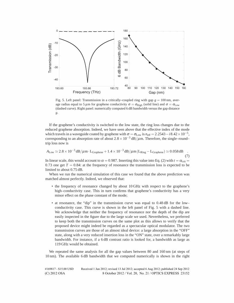
Fig. 5. Left panel: Transmission in a critically–coupled ring with gap g = 100 nm, aver-age radius equal to 5 μm for graphene conductivity σ = σHigh (solid line) and σ = σLow(dashed curve). Right panel: numerically computed 6 dB bandwidth versus the gap distanceg.
If the graphene’s conductivity is switched to the low state, the ring loss changes due to thereduced graphene absorption. Indeed, we have seen above that the effective index of the modewhich travels in a waveguide coated by graphene with σ =σLow is neff = 2.2543− i8.42×10−5,corresponding to an absorption rate of about 2.8×10⁻³ dB/μm. Therefore, the single–round–trip loss now is
ALow � 2.8×10⁻³ dB/μm ·LGraphene +1.4×10⁻³ dB/μm(LRing −LGraphene)� 0.058dB .(7)
In linear scale, this would account to α = 0.987. Inserting this value into Eq. (2) with t =αcrit =0.73 one get T = 0.84: at the frequency of resonance the transmission loss is expected to belimited to about 0.75 dB.
When we run the numerical simulation of this case we found that the above prediction wasmatched almost perfectly. Indeed, we observed that:
• the frequency of resonance changed by about 10 GHz with respect to the graphene’shigh–conductivity case. This in turn confirms that graphene’s conductivity has a veryminor effect on the phase constant of the mode;
• at resonance, the “dip” in the transmission curve was equal to 0.48 dB for the low–conductivity case. This curve is shown in the left panel of Fig. 5 with a dashed line.We acknowledge that neither the frequency of resonance nor the depth of the dip areeasily inspected in the figure due to the large scale we used. Nevertheless, we preferredto keep both the transmission curves on the same plot as this allows to verify that theproposed device might indeed be regarded as a spectacular optical modulator. The twotransmission curves are those of an almost ideal device: a large absorption in the “OFF”state, along with a very reduced insertion loss in the “ON” state, over a remarkably largebandwidth. For instance, if a 6 dB contrast ratio is looked for, a bandwidth as large as119 GHz would be obtained.
We repeated the same analysis for all the gap values between 80 and 160 nm (at steps of10 nm). The available 6 dB bandwidth that we computed numerically is shown in the right
#169817 - $15.00 USD Received 1 Jun 2012; revised 13 Jul 2012; accepted 6 Aug 2012; published 24 Sep 2012(C) 2012 OSA 8 October 2012 / Vol. 20, No. 21 / OPTICS EXPRESS 23152
panel of Fig. 5 as a function of the gap distance g. In all the cases, the insertion losses wemeasured never exceeded the level of 0.5 dB.
5. An estimate of the energy required for switch
Graphene’s conductivity can be changed by adding (or removing) electrical charges on it. Thiscan be done by realizing a capacitor in which one or both the armatures are formed by graphenelayers. Liu et coauthors have shown experimentally both the configurations (see Fig. 1 of ref.[20] and Fig. 1 of ref. [21] for the single and double layer configurations, respectively). Also,they suggested that the double–layer configuration is the best one, as this allows to avoid useof lossy doped silicon to form one of the electrical contacts. In addition, the presence of twographene layers doubles the effects of the graphene itself.
Observe in our case that lower values of graphene’s conductivity are obtained when thecharge concentration is raised (see Fig. 3). Also observe in the left panel of Fig. 5 that lowgraphene’s conductivity brings the modulator to its “ON” (i.e. transmitting) state. The reverseapplies by lowering the charge concentration. This explains the choice of subscripts we madebelow Eq. (5).
The structure we have used in our simulations follows Liu’s suggestion: two sheets ofgraphene sandwich a layer of alumina and form the capacitor (see paragraph 2.1). Estimateof the energy required for switching is a trivial application of the capacitor paradox problem.For a pseudo–random bit–sequence this yields
EPRBS =12
Q2ON −Q2
OFF
2C
The 1/2 factor accounts for the fact that in a random sequence, switch from bit “0” to bit “1”(or viceversa) only happens one half of the times. The amount of charge required to bring themodulator to the “ON” state is
QON = ρON eS , S = ψGraphene RAve W
with e the electron charge and S the extension of the area covered with graphene with RAve thering average radius, and W the ring waveguide width, respectively. An analogous expressionholds for the “OFF” state too. Neglecting fringing effects, the capacitance of the graphene–alumina–graphene structure is
C = ε0εrel,dielS
hdiel
with εrel,diel and hdiel the relative dielectric constant and thickness of the dielectric oxide be-tween the graphene sheets respectively. The voltage required for charging is
VON,OFF =QON,OFF
C=
ρON,OFFeε0 εrel,diel
hdiel (8)
and the energy required for switching
EPRBS =12(ρ2
ON −ρ2OFF)e2 hdielS
2ε0εrel,diel. (9)
Some interesting relationships in Eq. (9) are worth of mention:
• Graphene’s surface S. The charging voltage is independent on S. Whereas, the switchingenergy linearly scales with it. In this respect, the present configuration might turn out tobe advantageous with respect to those of refs. [20, 21] because of the reduced amount ofgraphene we needed to use here.
#169817 - $15.00 USD Received 1 Jun 2012; revised 13 Jul 2012; accepted 6 Aug 2012; published 24 Sep 2012(C) 2012 OSA 8 October 2012 / Vol. 20, No. 21 / OPTICS EXPRESS 23153
• Oxide’s thickness hdiel. Both the voltage and the energy scale linearly with it.
• Oxide’s dielectric constant εrel,diel. Both the voltage and the energy scale inversely withit.
Fig. 6. Left panel: Estimate of the energy required for switching with a pseudo–random bit–sequence (PRBS) in a ring modulator with oxide being constituted by a 7 nm thick layer ofalumina (εrel,diel = 10 at microwaves). Right panel: numerically evaluated dependence ofthe required switching energy versus the available bandwidth.
A plot of Eq. (9) for oxide being constituted by a 7 nm thick layer of alumina (εrel,diel = 10at microwave frequencies) is shown in Fig. 6. Also shown in the figure is the dependence ofthe energy required for switching as a function of the available bandwidth. A nice linear fit isfound, with a pace of about 5 fJ for each 10 GHz increase of the bandwidth.
It is also observed that energies below the level of 100 fJ/bit are estimated for all the valuesof gap. In addition, from Eq. (8), it is also found that voltages equal to 0.9 and 2.6V would beneeded to drive the modulator to the OFF and ON states, respectively. However, it is remarkedthat, according to the parameters’ list of dependencies we have listed above, these values couldbe further reduced if an oxide layer with either thinner dimensions or higher refractive indexwere used. For instance, if a 3 nm thick oxide were realized, the energy required for switchingwould drop to the range of 10÷30 fJ/bit, the pace of growth with bandwidth extension would bereduced to about 2 fJ for additional 10 GHz and, most important, the voltages needed to drivethe modulator would fall below 1.2 V, i.e. it would become compatible with state of the artlow–voltage CMOS requirements.
A rough estimate of heating effects can also be made. To this end, we first notice thatgraphene has been proved to be an excellent thermal conductor [30], while the silica claddingwhich surrounds the whole structure is a thermal insulator. As a consequence, any heating dueto dissipation in the graphene layers is transferred very efficiently to the silicon core, whicheventually acts as a sort of heat sink for the whole structure.
In the OFF state of the modulator, the light injected in the ring is absorbed by graphene. Inorder to estimate the change of temperature due to this absorption, we start from the experimen-tal results reported by DeRose and coauthors in ref. [31]. They have shown that the response ofa silicon microring can be tuned thermally by dissipating electrical power. The rate of tuningis in the order of 4.4 μW/GHz. Hence, if the ring is fed with a 1 mW continuous–wave laserlight, and since this light is absorbed by graphene only for one half of the time, a shift in the
#169817 - $15.00 USD Received 1 Jun 2012; revised 13 Jul 2012; accepted 6 Aug 2012; published 24 Sep 2012(C) 2012 OSA 8 October 2012 / Vol. 20, No. 21 / OPTICS EXPRESS 23154
the resonant frequency in the order of 125 GHz may be expected when comparing operationsin the “cold” and “heated” graphene cases. Remark that this is a thermal effect. That is, thefrequency shift can not and does not follow the modulation repetition rate, and only dependson the average level of dissipated power. The frequency of operation of the modulator sets at asteady value after initial thermalization has been completed.
Physically, the 125 GHz shift of the resonant frequency is due to a change of silicon refractiveindex. One may assume that
ΔnSi
nSi� Δ f
f→ ΔnSi � 0.125THz
200THz
√12 � 2×10⁻³ .
Since the thermo-optic coefficient of silicon is in the order of 2× 10⁻⁴ K−1, a temperaturechange in the order of ten degrees is therefore expected in silicon (and graphene) when oper-ating the modulator. With respect to room temperatures, this represent less that a 5% change, sothat the effect on both the Fermi–Dirac distribution and the complex conductivity of graphene isexpected to be rather modest. Presence of cooling devices outside the modulator might furtherdecrease this effect.
6. Conclusion
We have proposed a novel device which exploits controllability of graphene’s optical conduc-tivity to realize a critically–coupled ring–modulator based on the physical mechanism first in-troduced by Yariv in ref. [1]. The modulator is designed to be at the critical condition for highgraphene’s conductivity. In this state, no light is transmitted from the input to the output port.Whereas, when graphene’s conductivity is switched to its low state, propagation in the ringbecomes almost lossless, and a dramatic increase of the transmitted power is observed.
Notice that we deliberately added losses to the propagation in the ring through insertion ofgraphene. This way, the overall Q–factor of the ring turned out to be rather low and no sharpresonances were formed. This is the major difference with respect to ring modulators basedon the plasma–dispersion–induced effect. Indeed, in those modulators, ON–OFF switching isobtained by changing the refractive index in the ring, causing this way a detune of the frequencyof resonance. However, since the change of refractive index one may reasonably obtain is small,a sharp transmission resonance is needed in order to realize a respectable contrast ratio. Typicalvalues of bandwidth that can be obtained in this way are in the order of 10÷20 GHz. On thecontrary, our design does not rely on frequency detuning. This in turn means that it may workwith broad resonances too, as we proved with the help of numerical simulations. Bandwidths inthe range of 100 GHz were found, though larger ones might actually be obtained if gap smallerthan 100 nm could be manufactured.
Observe that a bandwidth in the order of 100 GHz is not merely a valuable figure of meritbecause of the transmission rates this modulator could work at. Actually, such a large bandwidthcould allow to get rid of temperature control circuits that are usually needed to lock a sharpresonance to the right wavelength. Keeping in mind that the power consumption of these controlcircuits greatly exceeds those of the modulators themselves, the present device could eventuallylead to a dramatic reduction of the energy required for switching which, in our case, could reallyapproach the level of few fJ per bit.
#169817 - $15.00 USD Received 1 Jun 2012; revised 13 Jul 2012; accepted 6 Aug 2012; published 24 Sep 2012(C) 2012 OSA 8 October 2012 / Vol. 20, No. 21 / OPTICS EXPRESS 23155
![Analysis of an electro-optic modulator based on a graphene …otip.sjtu.edu.cn/publication/Journal/2015-OE-PanTing-Analysis of an... · several tens of micrometers [6, 7], resulting](https://img.pdfslide.net/doc/110x75/5c41637593f3c338e1322b25/analysis-of-an-electro-optic-modulator-based-on-a-graphene-otipsjtueducnpublicationjournal2015-oe-panting-analysis.jpg)


![High-Speed Plasmonic-Silicon Modulator Driven by Epsilon ...graphene [5], [6], electro-optic polymer[7], [8], and phase change materials [9]. Such hybrid plasmonic-silicon photonic](https://img.pdfslide.net/doc/110x75/60bafd81731e884d3b7afae2/high-speed-plasmonic-silicon-modulator-driven-by-epsilon-graphene-5-6.jpg)