Embed Size (px)
Citation preview


GSM Design Library
1
Advanced Design System 2011
September 2011GSM Design Library

GSM Design Library
2
© Agilent Technologies, Inc. 2000-20115301 Stevens Creek Blvd., Santa Clara, CA 95052 USANo part of this documentation may be reproduced in any form or by any means (includingelectronic storage and retrieval or translation into a foreign language) without prioragreement and written consent from Agilent Technologies, Inc. as governed by UnitedStates and international copyright laws.
AcknowledgmentsMentor Graphics is a trademark of Mentor Graphics Corporation in the U.S. and othercountries. Mentor products and processes are registered trademarks of Mentor GraphicsCorporation. * Calibre is a trademark of Mentor Graphics Corporation in the US and othercountries. "Microsoft®, Windows®, MS Windows®, Windows NT®, Windows 2000® andWindows Internet Explorer® are U.S. registered trademarks of Microsoft Corporation.Pentium® is a U.S. registered trademark of Intel Corporation. PostScript® and Acrobat®are trademarks of Adobe Systems Incorporated. UNIX® is a registered trademark of theOpen Group. Oracle and Java and registered trademarks of Oracle and/or its affiliates.Other names may be trademarks of their respective owners. SystemC® is a registeredtrademark of Open SystemC Initiative, Inc. in the United States and other countries and isused with permission. MATLAB® is a U.S. registered trademark of The Math Works, Inc..HiSIM2 source code, and all copyrights, trade secrets or other intellectual property rightsin and to the source code in its entirety, is owned by Hiroshima University and STARC.FLEXlm is a trademark of Globetrotter Software, Incorporated. Layout Boolean Engine byKlaas Holwerda, v1.7 http://www.xs4all.nl/~kholwerd/bool.html . FreeType Project,Copyright (c) 1996-1999 by David Turner, Robert Wilhelm, and Werner Lemberg.QuestAgent search engine (c) 2000-2002, JObjects. Motif is a trademark of the OpenSoftware Foundation. Netscape is a trademark of Netscape Communications Corporation.Netscape Portable Runtime (NSPR), Copyright (c) 1998-2003 The Mozilla Organization. Acopy of the Mozilla Public License is at http://www.mozilla.org/MPL/ . FFTW, The FastestFourier Transform in the West, Copyright (c) 1997-1999 Massachusetts Institute ofTechnology. All rights reserved.
The following third-party libraries are used by the NlogN Momentum solver:
"This program includes Metis 4.0, Copyright © 1998, Regents of the University ofMinnesota", http://www.cs.umn.edu/~metis , METIS was written by George Karypis([email protected]).
Intel@ Math Kernel Library, http://www.intel.com/software/products/mkl
SuperLU_MT version 2.0 - Copyright © 2003, The Regents of the University of California,through Lawrence Berkeley National Laboratory (subject to receipt of any requiredapprovals from U.S. Dept. of Energy). All rights reserved. SuperLU Disclaimer: THISSOFTWARE IS PROVIDED BY THE COPYRIGHT HOLDERS AND CONTRIBUTORS "AS IS"AND ANY EXPRESS OR IMPLIED WARRANTIES, INCLUDING, BUT NOT LIMITED TO, THEIMPLIED WARRANTIES OF MERCHANTABILITY AND FITNESS FOR A PARTICULAR PURPOSEARE DISCLAIMED. IN NO EVENT SHALL THE COPYRIGHT OWNER OR CONTRIBUTORS BELIABLE FOR ANY DIRECT, INDIRECT, INCIDENTAL, SPECIAL, EXEMPLARY, ORCONSEQUENTIAL DAMAGES (INCLUDING, BUT NOT LIMITED TO, PROCUREMENT OFSUBSTITUTE GOODS OR SERVICES; LOSS OF USE, DATA, OR PROFITS; OR BUSINESSINTERRUPTION) HOWEVER CAUSED AND ON ANY THEORY OF LIABILITY, WHETHER IN

GSM Design Library
3
CONTRACT, STRICT LIABILITY, OR TORT (INCLUDING NEGLIGENCE OR OTHERWISE)ARISING IN ANY WAY OUT OF THE USE OF THIS SOFTWARE, EVEN IF ADVISED OF THEPOSSIBILITY OF SUCH DAMAGE.
7-zip - 7-Zip Copyright: Copyright (C) 1999-2009 Igor Pavlov. Licenses for files are:7z.dll: GNU LGPL + unRAR restriction, All other files: GNU LGPL. 7-zip License: This libraryis free software; you can redistribute it and/or modify it under the terms of the GNULesser General Public License as published by the Free Software Foundation; eitherversion 2.1 of the License, or (at your option) any later version. This library is distributedin the hope that it will be useful,but WITHOUT ANY WARRANTY; without even the impliedwarranty of MERCHANTABILITY or FITNESS FOR A PARTICULAR PURPOSE. See the GNULesser General Public License for more details. You should have received a copy of theGNU Lesser General Public License along with this library; if not, write to the FreeSoftware Foundation, Inc., 59 Temple Place, Suite 330, Boston, MA 02111-1307 USA.unRAR copyright: The decompression engine for RAR archives was developed using sourcecode of unRAR program.All copyrights to original unRAR code are owned by AlexanderRoshal. unRAR License: The unRAR sources cannot be used to re-create the RARcompression algorithm, which is proprietary. Distribution of modified unRAR sources inseparate form or as a part of other software is permitted, provided that it is clearly statedin the documentation and source comments that the code may not be used to develop aRAR (WinRAR) compatible archiver. 7-zip Availability: http://www.7-zip.org/
AMD Version 2.2 - AMD Notice: The AMD code was modified. Used by permission. AMDcopyright: AMD Version 2.2, Copyright © 2007 by Timothy A. Davis, Patrick R. Amestoy,and Iain S. Duff. All Rights Reserved. AMD License: Your use or distribution of AMD or anymodified version of AMD implies that you agree to this License. This library is freesoftware; you can redistribute it and/or modify it under the terms of the GNU LesserGeneral Public License as published by the Free Software Foundation; either version 2.1 ofthe License, or (at your option) any later version. This library is distributed in the hopethat it will be useful, but WITHOUT ANY WARRANTY; without even the implied warranty ofMERCHANTABILITY or FITNESS FOR A PARTICULAR PURPOSE. See the GNU LesserGeneral Public License for more details. You should have received a copy of the GNULesser General Public License along with this library; if not, write to the Free SoftwareFoundation, Inc., 51 Franklin St, Fifth Floor, Boston, MA 02110-1301 USA Permission ishereby granted to use or copy this program under the terms of the GNU LGPL, providedthat the Copyright, this License, and the Availability of the original version is retained onall copies.User documentation of any code that uses this code or any modified version ofthis code must cite the Copyright, this License, the Availability note, and "Used bypermission." Permission to modify the code and to distribute modified code is granted,provided the Copyright, this License, and the Availability note are retained, and a noticethat the code was modified is included. AMD Availability:http://www.cise.ufl.edu/research/sparse/amd
UMFPACK 5.0.2 - UMFPACK Notice: The UMFPACK code was modified. Used by permission.UMFPACK Copyright: UMFPACK Copyright © 1995-2006 by Timothy A. Davis. All RightsReserved. UMFPACK License: Your use or distribution of UMFPACK or any modified versionof UMFPACK implies that you agree to this License. This library is free software; you canredistribute it and/or modify it under the terms of the GNU Lesser General Public Licenseas published by the Free Software Foundation; either version 2.1 of the License, or (atyour option) any later version. This library is distributed in the hope that it will be useful,but WITHOUT ANY WARRANTY; without even the implied warranty of MERCHANTABILITY

GSM Design Library
4
or FITNESS FOR A PARTICULAR PURPOSE. See the GNU Lesser General Public License formore details. You should have received a copy of the GNU Lesser General Public Licensealong with this library; if not, write to the Free Software Foundation, Inc., 51 Franklin St,Fifth Floor, Boston, MA 02110-1301 USA Permission is hereby granted to use or copy thisprogram under the terms of the GNU LGPL, provided that the Copyright, this License, andthe Availability of the original version is retained on all copies. User documentation of anycode that uses this code or any modified version of this code must cite the Copyright, thisLicense, the Availability note, and "Used by permission." Permission to modify the codeand to distribute modified code is granted, provided the Copyright, this License, and theAvailability note are retained, and a notice that the code was modified is included.UMFPACK Availability: http://www.cise.ufl.edu/research/sparse/umfpack UMFPACK(including versions 2.2.1 and earlier, in FORTRAN) is available athttp://www.cise.ufl.edu/research/sparse . MA38 is available in the Harwell SubroutineLibrary. This version of UMFPACK includes a modified form of COLAMD Version 2.0,originally released on Jan. 31, 2000, also available athttp://www.cise.ufl.edu/research/sparse . COLAMD V2.0 is also incorporated as a built-infunction in MATLAB version 6.1, by The MathWorks, Inc. http://www.mathworks.com .COLAMD V1.0 appears as a column-preordering in SuperLU (SuperLU is available athttp://www.netlib.org ). UMFPACK v4.0 is a built-in routine in MATLAB 6.5. UMFPACK v4.3is a built-in routine in MATLAB 7.1.
Qt Version 4.6.3 - Qt Notice: The Qt code was modified. Used by permission. Qt copyright:Qt Version 4.6.3, Copyright (c) 2010 by Nokia Corporation. All Rights Reserved. QtLicense: Your use or distribution of Qt or any modified version of Qt implies that you agreeto this License. This library is free software; you can redistribute it and/or modify it undertheterms of the GNU Lesser General Public License as published by the Free SoftwareFoundation; either version 2.1 of the License, or (at your option) any later version. Thislibrary is distributed in the hope that it will be useful,but WITHOUT ANY WARRANTY; without even the implied warranty of MERCHANTABILITYor FITNESS FOR A PARTICULAR PURPOSE. See the GNU Lesser General Public License formore details. You should have received a copy of the GNU Lesser General Public Licensealong with this library; if not, write to the Free Software Foundation, Inc., 51 Franklin St,Fifth Floor, Boston, MA 02110-1301 USA Permission is hereby granted to use or copy thisprogram under the terms of the GNU LGPL, provided that the Copyright, this License, andthe Availability of the original version is retained on all copies.Userdocumentation of any code that uses this code or any modified version of this code mustcite the Copyright, this License, the Availability note, and "Used by permission."Permission to modify the code and to distribute modified code is granted, provided theCopyright, this License, and the Availability note are retained, and a notice that the codewas modified is included. Qt Availability: http://www.qtsoftware.com/downloads PatchesApplied to Qt can be found in the installation at:$HPEESOF_DIR/prod/licenses/thirdparty/qt/patches. You may also contact BrianBuchanan at Agilent Inc. at [email protected] for more information.
The HiSIM_HV source code, and all copyrights, trade secrets or other intellectual propertyrights in and to the source code, is owned by Hiroshima University and/or STARC.
Errata The ADS product may contain references to "HP" or "HPEESOF" such as in filenames and directory names. The business entity formerly known as "HP EEsof" is now partof Agilent Technologies and is known as "Agilent EEsof". To avoid broken functionality and

GSM Design Library
5
to maintain backward compatibility for our customers, we did not change all the namesand labels that contain "HP" or "HPEESOF" references.
Warranty The material contained in this document is provided "as is", and is subject tobeing changed, without notice, in future editions. Further, to the maximum extentpermitted by applicable law, Agilent disclaims all warranties, either express or implied,with regard to this documentation and any information contained herein, including but notlimited to the implied warranties of merchantability and fitness for a particular purpose.Agilent shall not be liable for errors or for incidental or consequential damages inconnection with the furnishing, use, or performance of this document or of anyinformation contained herein. Should Agilent and the user have a separate writtenagreement with warranty terms covering the material in this document that conflict withthese terms, the warranty terms in the separate agreement shall control.
Technology Licenses The hardware and/or software described in this document arefurnished under a license and may be used or copied only in accordance with the terms ofsuch license. Portions of this product include the SystemC software licensed under OpenSource terms, which are available for download at http://systemc.org/ . This software isredistributed by Agilent. The Contributors of the SystemC software provide this software"as is" and offer no warranty of any kind, express or implied, including without limitationwarranties or conditions or title and non-infringement, and implied warranties orconditions merchantability and fitness for a particular purpose. Contributors shall not beliable for any damages of any kind including without limitation direct, indirect, special,incidental and consequential damages, such as lost profits. Any provisions that differ fromthis disclaimer are offered by Agilent only.
Restricted Rights Legend U.S. Government Restricted Rights. Software and technicaldata rights granted to the federal government include only those rights customarilyprovided to end user customers. Agilent provides this customary commercial license inSoftware and technical data pursuant to FAR 12.211 (Technical Data) and 12.212(Computer Software) and, for the Department of Defense, DFARS 252.227-7015(Technical Data - Commercial Items) and DFARS 227.7202-3 (Rights in CommercialComputer Software or Computer Software Documentation).

GSM Design Library
6
About GSM Design Library . . . . . . . . . . . . . . . . . . . . . . . . . . . . . . . . . . . . . . . . . . . . . . . . . 9 Channel Coding Components for GSM Design Library . . . . . . . . . . . . . . . . . . . . . . . . . . . . . . . 22
GSM_BlockCodeRACH . . . . . . . . . . . . . . . . . . . . . . . . . . . . . . . . . . . . . . . . . . . . . . . . . . 23 GSM_CC_WithTail . . . . . . . . . . . . . . . . . . . . . . . . . . . . . . . . . . . . . . . . . . . . . . . . . . . 23 GSM_Combiner . . . . . . . . . . . . . . . . . . . . . . . . . . . . . . . . . . . . . . . . . . . . . . . . . . . . . 28 GSM_CycDecoder . . . . . . . . . . . . . . . . . . . . . . . . . . . . . . . . . . . . . . . . . . . . . . . . . . . 28 GSM_CycEncoder . . . . . . . . . . . . . . . . . . . . . . . . . . . . . . . . . . . . . . . . . . . . . . . . . . . 34 GSM_DCC_WithTail . . . . . . . . . . . . . . . . . . . . . . . . . . . . . . . . . . . . . . . . . . . . . . . . . . 37 GSM_Deinterleaver_4 . . . . . . . . . . . . . . . . . . . . . . . . . . . . . . . . . . . . . . . . . . . . . . . . 40 GSM_Deinterleaver_8 . . . . . . . . . . . . . . . . . . . . . . . . . . . . . . . . . . . . . . . . . . . . . . . . 40 GSM_Deinterleaver_F96 . . . . . . . . . . . . . . . . . . . . . . . . . . . . . . . . . . . . . . . . . . . . . . . 42 GSM_Depuncture . . . . . . . . . . . . . . . . . . . . . . . . . . . . . . . . . . . . . . . . . . . . . . . . . . . 44 GSM_FACCH_Decoder . . . . . . . . . . . . . . . . . . . . . . . . . . . . . . . . . . . . . . . . . . . . . . . . 46 GSM_FACCH_Encoder . . . . . . . . . . . . . . . . . . . . . . . . . . . . . . . . . . . . . . . . . . . . . . . . 50 GSM_FireDecoder . . . . . . . . . . . . . . . . . . . . . . . . . . . . . . . . . . . . . . . . . . . . . . . . . . . . . 54 GSM_Interleaver_4 . . . . . . . . . . . . . . . . . . . . . . . . . . . . . . . . . . . . . . . . . . . . . . . . . . 57 GSM_Interleaver_8 . . . . . . . . . . . . . . . . . . . . . . . . . . . . . . . . . . . . . . . . . . . . . . . . . . 60 GSM_Interleaver_F96 . . . . . . . . . . . . . . . . . . . . . . . . . . . . . . . . . . . . . . . . . . . . . . . . 63 GSM_InverseReord . . . . . . . . . . . . . . . . . . . . . . . . . . . . . . . . . . . . . . . . . . . . . . . . . . 66 GSM_Puncture . . . . . . . . . . . . . . . . . . . . . . . . . . . . . . . . . . . . . . . . . . . . . . . . . . . . . 66 GSM_RACH_Decoder . . . . . . . . . . . . . . . . . . . . . . . . . . . . . . . . . . . . . . . . . . . . . . . . . 68 GSM_RACH_Encoder . . . . . . . . . . . . . . . . . . . . . . . . . . . . . . . . . . . . . . . . . . . . . . . . . 73 GSM_Reorder . . . . . . . . . . . . . . . . . . . . . . . . . . . . . . . . . . . . . . . . . . . . . . . . . . . . . . 76 GSM_RmvStlFlgs . . . . . . . . . . . . . . . . . . . . . . . . . . . . . . . . . . . . . . . . . . . . . . . . . . . . 76 GSM_SACCH_Decoder . . . . . . . . . . . . . . . . . . . . . . . . . . . . . . . . . . . . . . . . . . . . . . . . . . 78 GSM_SACCH_Encoder . . . . . . . . . . . . . . . . . . . . . . . . . . . . . . . . . . . . . . . . . . . . . . . . 83 GSM_SCH_Decoder . . . . . . . . . . . . . . . . . . . . . . . . . . . . . . . . . . . . . . . . . . . . . . . . . . 86 GSM_SCH_Encoder . . . . . . . . . . . . . . . . . . . . . . . . . . . . . . . . . . . . . . . . . . . . . . . . . . 86 GSM_Splitter . . . . . . . . . . . . . . . . . . . . . . . . . . . . . . . . . . . . . . . . . . . . . . . . . . . . . . 88 GSM_TailBits . . . . . . . . . . . . . . . . . . . . . . . . . . . . . . . . . . . . . . . . . . . . . . . . . . . . . . . 90 GSM_TCHF24_Decoder . . . . . . . . . . . . . . . . . . . . . . . . . . . . . . . . . . . . . . . . . . . . . . . 92 GSM_TCHF24_Encoder . . . . . . . . . . . . . . . . . . . . . . . . . . . . . . . . . . . . . . . . . . . . . . . . 94 GSM_TCHF48_Decoder . . . . . . . . . . . . . . . . . . . . . . . . . . . . . . . . . . . . . . . . . . . . . . . 99 GSM_TCHF48_Encoder . . . . . . . . . . . . . . . . . . . . . . . . . . . . . . . . . . . . . . . . . . . . . . . . 99 GSM_TCHF96_Decoder . . . . . . . . . . . . . . . . . . . . . . . . . . . . . . . . . . . . . . . . . . . . . . . 104 GSM_TCHF96_Encoder . . . . . . . . . . . . . . . . . . . . . . . . . . . . . . . . . . . . . . . . . . . . . . . . 104 GSM_TCHFS_Decoder . . . . . . . . . . . . . . . . . . . . . . . . . . . . . . . . . . . . . . . . . . . . . . . . 109 GSM_TCHFS_Encoder . . . . . . . . . . . . . . . . . . . . . . . . . . . . . . . . . . . . . . . . . . . . . . . . 112
Equalization Components for GSM Design Library . . . . . . . . . . . . . . . . . . . . . . . . . . . . . . . . . . 115 GSM_ChannelEstimator . . . . . . . . . . . . . . . . . . . . . . . . . . . . . . . . . . . . . . . . . . . . . . . 116 GSM_Derotator . . . . . . . . . . . . . . . . . . . . . . . . . . . . . . . . . . . . . . . . . . . . . . . . . . . . . 119 GSM_Equalizer . . . . . . . . . . . . . . . . . . . . . . . . . . . . . . . . . . . . . . . . . . . . . . . . . . . . . 119 GSM_EquCombiner . . . . . . . . . . . . . . . . . . . . . . . . . . . . . . . . . . . . . . . . . . . . . . . . . . 124 GSM_EquComposeAB . . . . . . . . . . . . . . . . . . . . . . . . . . . . . . . . . . . . . . . . . . . . . . . . . 127 GSM_EquDecomposeAB . . . . . . . . . . . . . . . . . . . . . . . . . . . . . . . . . . . . . . . . . . . . . . . 130 GSM_EquSplitter . . . . . . . . . . . . . . . . . . . . . . . . . . . . . . . . . . . . . . . . . . . . . . . . . . . . 133 GSM_Filter . . . . . . . . . . . . . . . . . . . . . . . . . . . . . . . . . . . . . . . . . . . . . . . . . . . . . . . . 136 GSM_Receiver . . . . . . . . . . . . . . . . . . . . . . . . . . . . . . . . . . . . . . . . . . . . . . . . . . . . . . 136 GSM_ReceiverAB . . . . . . . . . . . . . . . . . . . . . . . . . . . . . . . . . . . . . . . . . . . . . . . . . . . . 141
Framing Components for GSM Design Library . . . . . . . . . . . . . . . . . . . . . . . . . . . . . . . . . . . . 144 GSM_AccessBurst . . . . . . . . . . . . . . . . . . . . . . . . . . . . . . . . . . . . . . . . . . . . . . . . . . . 145

GSM Design Library
7
GSM_BcchCcch4SdcchDn . . . . . . . . . . . . . . . . . . . . . . . . . . . . . . . . . . . . . . . . . . . . . . 145 GSM_BcchCcch4SdcchUp . . . . . . . . . . . . . . . . . . . . . . . . . . . . . . . . . . . . . . . . . . . . . . 150 GSM_BcchCcchDn . . . . . . . . . . . . . . . . . . . . . . . . . . . . . . . . . . . . . . . . . . . . . . . . . . . 153 GSM_BcchCcchUp . . . . . . . . . . . . . . . . . . . . . . . . . . . . . . . . . . . . . . . . . . . . . . . . . . . 156 GSM_DeAccessBurst . . . . . . . . . . . . . . . . . . . . . . . . . . . . . . . . . . . . . . . . . . . . . . . . . 156 GSM_DeBcchCcch4SdcchDn . . . . . . . . . . . . . . . . . . . . . . . . . . . . . . . . . . . . . . . . . . . . 158 GSM_DeBcchCcch4SdcchUp . . . . . . . . . . . . . . . . . . . . . . . . . . . . . . . . . . . . . . . . . . . . 163 GSM_DeBcchCcchDn . . . . . . . . . . . . . . . . . . . . . . . . . . . . . . . . . . . . . . . . . . . . . . . . . 166 GSM_DeMultiframe26 . . . . . . . . . . . . . . . . . . . . . . . . . . . . . . . . . . . . . . . . . . . . . . . . 169 GSM_DeNormalBurst . . . . . . . . . . . . . . . . . . . . . . . . . . . . . . . . . . . . . . . . . . . . . . . . . 172 GSM_DeSBurst . . . . . . . . . . . . . . . . . . . . . . . . . . . . . . . . . . . . . . . . . . . . . . . . . . . . . 172 GSM_DeSdcch8Dn . . . . . . . . . . . . . . . . . . . . . . . . . . . . . . . . . . . . . . . . . . . . . . . . . . . 174 GSM_DeSdcch8Up . . . . . . . . . . . . . . . . . . . . . . . . . . . . . . . . . . . . . . . . . . . . . . . . . . . 179 GSM_DeTDMA . . . . . . . . . . . . . . . . . . . . . . . . . . . . . . . . . . . . . . . . . . . . . . . . . . . . . . 182 GSM_DummyBurst . . . . . . . . . . . . . . . . . . . . . . . . . . . . . . . . . . . . . . . . . . . . . . . . . . 185 GSM_FBurst . . . . . . . . . . . . . . . . . . . . . . . . . . . . . . . . . . . . . . . . . . . . . . . . . . . . . . . 185 GSM_Multiframe26 . . . . . . . . . . . . . . . . . . . . . . . . . . . . . . . . . . . . . . . . . . . . . . . . . . 190 GSM_NormalBurst . . . . . . . . . . . . . . . . . . . . . . . . . . . . . . . . . . . . . . . . . . . . . . . . . . . 193 GSM_SBurst . . . . . . . . . . . . . . . . . . . . . . . . . . . . . . . . . . . . . . . . . . . . . . . . . . . . . . . 196 GSM_Sdcch8Dn . . . . . . . . . . . . . . . . . . . . . . . . . . . . . . . . . . . . . . . . . . . . . . . . . . . . . 199 GSM_Sdcch8Up . . . . . . . . . . . . . . . . . . . . . . . . . . . . . . . . . . . . . . . . . . . . . . . . . . . . . 202 GSM_TDMA . . . . . . . . . . . . . . . . . . . . . . . . . . . . . . . . . . . . . . . . . . . . . . . . . . . . . . . . 205 GSM_TimeBaseCounter . . . . . . . . . . . . . . . . . . . . . . . . . . . . . . . . . . . . . . . . . . . . . . . 208
Measurement Components for GSM Design Library . . . . . . . . . . . . . . . . . . . . . . . . . . . . . . . . . 211 GSM_BerFer . . . . . . . . . . . . . . . . . . . . . . . . . . . . . . . . . . . . . . . . . . . . . . . . . . . . . . . 212 GSM_ErrPatternDisplay . . . . . . . . . . . . . . . . . . . . . . . . . . . . . . . . . . . . . . . . . . . . . . . 212
Modem Components . . . . . . . . . . . . . . . . . . . . . . . . . . . . . . . . . . . . . . . . . . . . . . . . . . . . . . 214 GSM_AQuarterBitAdd . . . . . . . . . . . . . . . . . . . . . . . . . . . . . . . . . . . . . . . . . . . . . . . . . 214 GSM_AQuarterBitRmv . . . . . . . . . . . . . . . . . . . . . . . . . . . . . . . . . . . . . . . . . . . . . . . . 220 GSM_Carrier . . . . . . . . . . . . . . . . . . . . . . . . . . . . . . . . . . . . . . . . . . . . . . . . . . . . . . . 223 GSM_DifferDecoder . . . . . . . . . . . . . . . . . . . . . . . . . . . . . . . . . . . . . . . . . . . . . . . . . . 226 GSM_DifferEncoder . . . . . . . . . . . . . . . . . . . . . . . . . . . . . . . . . . . . . . . . . . . . . . . . . . 226 GSM_GMSKDemod . . . . . . . . . . . . . . . . . . . . . . . . . . . . . . . . . . . . . . . . . . . . . . . . . . 228 GSM_GMSKMod . . . . . . . . . . . . . . . . . . . . . . . . . . . . . . . . . . . . . . . . . . . . . . . . . . . . . 233 GSM_MpyClock . . . . . . . . . . . . . . . . . . . . . . . . . . . . . . . . . . . . . . . . . . . . . . . . . . . . . 236 GSM_Rom . . . . . . . . . . . . . . . . . . . . . . . . . . . . . . . . . . . . . . . . . . . . . . . . . . . . . . . . 236
Speech Codec Components . . . . . . . . . . . . . . . . . . . . . . . . . . . . . . . . . . . . . . . . . . . . . . . . . 241 GSM_APCM_Quantizer . . . . . . . . . . . . . . . . . . . . . . . . . . . . . . . . . . . . . . . . . . . . . . . . 242 GSM_Autocorrelation . . . . . . . . . . . . . . . . . . . . . . . . . . . . . . . . . . . . . . . . . . . . . . . . . 245 GSM_CodeLAR . . . . . . . . . . . . . . . . . . . . . . . . . . . . . . . . . . . . . . . . . . . . . . . . . . . . . 245 GSM_DecodeLAR . . . . . . . . . . . . . . . . . . . . . . . . . . . . . . . . . . . . . . . . . . . . . . . . . . . . 250 GSM_Deemphasis . . . . . . . . . . . . . . . . . . . . . . . . . . . . . . . . . . . . . . . . . . . . . . . . . . . 253 GSM_Deframing . . . . . . . . . . . . . . . . . . . . . . . . . . . . . . . . . . . . . . . . . . . . . . . . . . . . . . 253 GSM_Framing . . . . . . . . . . . . . . . . . . . . . . . . . . . . . . . . . . . . . . . . . . . . . . . . . . . . . . 257 GSM_Interpolation . . . . . . . . . . . . . . . . . . . . . . . . . . . . . . . . . . . . . . . . . . . . . . . . . . . 260 GSM_InverseAPCM . . . . . . . . . . . . . . . . . . . . . . . . . . . . . . . . . . . . . . . . . . . . . . . . . . 264 GSM_LARToRefCoe . . . . . . . . . . . . . . . . . . . . . . . . . . . . . . . . . . . . . . . . . . . . . . . . . . 264 GSM_LogAreaRatio . . . . . . . . . . . . . . . . . . . . . . . . . . . . . . . . . . . . . . . . . . . . . . . . . . 266 GSM_LongTermAnalysis . . . . . . . . . . . . . . . . . . . . . . . . . . . . . . . . . . . . . . . . . . . . . . . 268 GSM_LongTermSynthesis . . . . . . . . . . . . . . . . . . . . . . . . . . . . . . . . . . . . . . . . . . . . . . 272 GSM_LTP_Parameter . . . . . . . . . . . . . . . . . . . . . . . . . . . . . . . . . . . . . . . . . . . . . . . . . 276

GSM Design Library
8
GSM_OffsetCompensation . . . . . . . . . . . . . . . . . . . . . . . . . . . . . . . . . . . . . . . . . . . . . 279 GSM_Postprocessing . . . . . . . . . . . . . . . . . . . . . . . . . . . . . . . . . . . . . . . . . . . . . . . . . 282 GSM_Preemphasis . . . . . . . . . . . . . . . . . . . . . . . . . . . . . . . . . . . . . . . . . . . . . . . . . . . 282 GSM_ReadFile . . . . . . . . . . . . . . . . . . . . . . . . . . . . . . . . . . . . . . . . . . . . . . . . . . . . . . 284 GSM_RPE_GridPosition . . . . . . . . . . . . . . . . . . . . . . . . . . . . . . . . . . . . . . . . . . . . . . . . 286 GSM_RPE_GridSelection . . . . . . . . . . . . . . . . . . . . . . . . . . . . . . . . . . . . . . . . . . . . . . . 291 GSM_ScaleInput . . . . . . . . . . . . . . . . . . . . . . . . . . . . . . . . . . . . . . . . . . . . . . . . . . . . 294 GSM_Schur . . . . . . . . . . . . . . . . . . . . . . . . . . . . . . . . . . . . . . . . . . . . . . . . . . . . . . . . 294 GSM_ShortTermAnalysis . . . . . . . . . . . . . . . . . . . . . . . . . . . . . . . . . . . . . . . . . . . . . . 296 GSM_ShortTermPredict . . . . . . . . . . . . . . . . . . . . . . . . . . . . . . . . . . . . . . . . . . . . . . . 301 GSM_ShortTermSynthesis . . . . . . . . . . . . . . . . . . . . . . . . . . . . . . . . . . . . . . . . . . . . . 304 GSM_SpeechDecoder . . . . . . . . . . . . . . . . . . . . . . . . . . . . . . . . . . . . . . . . . . . . . . . . . 307 GSM_SpeechEncoder . . . . . . . . . . . . . . . . . . . . . . . . . . . . . . . . . . . . . . . . . . . . . . . . . 310 GSM_WeightingFilter . . . . . . . . . . . . . . . . . . . . . . . . . . . . . . . . . . . . . . . . . . . . . . . . . 314 GSM_WriteFile . . . . . . . . . . . . . . . . . . . . . . . . . . . . . . . . . . . . . . . . . . . . . . . . . . . . . 317
Synchronization Components for GSM Design Library . . . . . . . . . . . . . . . . . . . . . . . . . . . . . . . 317 GSM_DataSelection . . . . . . . . . . . . . . . . . . . . . . . . . . . . . . . . . . . . . . . . . . . . . . . . . . 317 GSM_PhaseRecovery . . . . . . . . . . . . . . . . . . . . . . . . . . . . . . . . . . . . . . . . . . . . . . . . . 323 GSM_PhsRcvryTrNoMod . . . . . . . . . . . . . . . . . . . . . . . . . . . . . . . . . . . . . . . . . . . . . . . 323 GSM_Sampler . . . . . . . . . . . . . . . . . . . . . . . . . . . . . . . . . . . . . . . . . . . . . . . . . . . . . . 325 GSM_SynABurst . . . . . . . . . . . . . . . . . . . . . . . . . . . . . . . . . . . . . . . . . . . . . . . . . . . . 329 GSM_SynNBurst . . . . . . . . . . . . . . . . . . . . . . . . . . . . . . . . . . . . . . . . . . . . . . . . . . . . 332 GSM_SynNBurstTrNoMod . . . . . . . . . . . . . . . . . . . . . . . . . . . . . . . . . . . . . . . . . . . . . . 335 GSM_SynSBurst . . . . . . . . . . . . . . . . . . . . . . . . . . . . . . . . . . . . . . . . . . . . . . . . . . . . 338 GSM_TrainBitGen . . . . . . . . . . . . . . . . . . . . . . . . . . . . . . . . . . . . . . . . . . . . . . . . . . . 341
GSM Design Examples . . . . . . . . . . . . . . . . . . . . . . . . . . . . . . . . . . . . . . . . . . . . . . . . . . . . . 344

GSM Design Library
9
About GSM Design Library
Introduction
GSM, the Global System for Mobile Communication, is a digital cellular radio system forpublic land mobile network (PLMN).
The GSM communication system is an important wireless system for the second-generation mobile communication. The GSM Design Library provides models that enableend-to-end system modeling and simulation for the physical layer of GSM systems. Thesemodels are intended to be a baseline system for designers to get an idea of what anominal of ideal system performance would be. They also can help the researchers in thisfield or GSM system designers to achieve their designs and improve their work efficiency.
The GSM Design Library includes key features of the GSM system in physical layer, forexample RPE-LTP speech codec, channel coding and interleaving (for channels such asTCH/FS, SACCH, RACH, SCH), burst assembly, GMSK modulation and demodulation, bitsynchronization, equalization, and FER and BER measurement.
The GSM example designs that are shipped with the GSM Design Library software,including schematics, test conditions, and simulation results, are described in GSM DesignExamples (gsm).
Overview of Component Libraries
The GSM Design Library includes more than 100 behavioral models and subnetworks thatare organized by their functions in seven libraries:
Speech Codec is part of the GSM system that provides the basic models required byETSI GSM 06.10, in which the specified transcoding procedure is applicable for thefull-rate traffic channel.Channel Coding includes cyclic codes encoder, cyclic codes decoder, reorder, Firecodes encoder and decoder, interleavers and de-interleavers per GSM specification.With these models, 13 kinds of GSM channels can be set up: TCH/FS, TCH/F9.6,TCH/F4.8, TCH/F2.4, SACCH, BCCH, PCH, AGCH, CBCH, SDCCH, FACCH, RACH, andSCH.Equalization includes derotator, splitter (splits one burst into two specific frames forbidirectional equalization), combiner (combines the two input frames into one burstafter bidirectional equalization), channel estimator, matched filter and equalizer.Framing includes bursts, time slots, TDMA frames, multiframe composing and de-composing.Measurement includes BER and FER measurement models.Modem includes GMSK modulation and demodulation (differential encoding anddecoding, Rom for I, Q branch signal).Synchronization includes data selection, phase recovery, and downsampler.

GSM Design Library
10
Twenty-nine sub-networks speed system construction, such as GMSK modulation,synchronization, receiver.
These models and sub-networks are implemented according to ETSI GSM specification.
TCH/FS example in Block Diagram of GSM TCH/FS System Simulation shows the systemsimulation structure. After speech codec, data is split by two splitters; the Ia part is cyclicencoded and the Ib part (132 bits) is not cyclic encoded. The combined Ia and Ib are themost critical bits that use half-rate convolutional coding after tail bits are added.Combined with the 78 part II bits, data (entire block length is 456 bits) is fed into thediagonal interleaver that enhances the error correction capability if a sequence of TDMAframes is corrupted during radio transmission. The interleaver output is sent to a burstassembly model (for example, normal burst).
In the reception side, bit synchronization and MLSE receiver are used to recover encodeddata. The BER and FER can be determined after comparing input and output data of thesystem.
Block Diagram of GSM TCH/FS System Simulation
Channel Coding
There are 13 channel types. The relationship between the channels and the modules are

GSM Design Library
11
shown in Channel Coding Modules.
Channel Coding Modules
ChannelType
Block Codec ConvolutionalCodec †
Interleaving, Deinterleaving
TCH/FS cyc_encoder, cyc_decoder,tailbits, reorder, inverse reorder,splitter, combiner
cc(2,1,5) interleaver_8, deinterleaver_8, (blockdiagonal interleaver) Get_stealing_flag
TCH/F96 tailbits puncturedcc(2,1,5)
interleaver_f96, deinterleaver_f96, (diagonalinterleaver) Get_stealing_flag
TCH/F48 tailbits cc(3,1,5) interleaver_f96,deinterleaver_f96,(diagonalinterleaver)Get_stealing_flag
TCH/F24 tailbits cc(6,1,5) interleaver_8,deinterleaver_8,(block diagonalinterleaver)Get_stealing_flag
SACCH,BCCH,PCH,AGCH,CBCH andSDCCH
cyc_encoder,Fire_decoder,tailbits
cc(2,1,5) interleaver_4, deinterleaver_4,(blockrectangular interleaver) Get_stealing_flag
FACCH cyc_encoder,Fire_decoder,tailbits
cc(2,1,5) interleaver_8, deinterleaver_8,(blockdiagonal interleaver) Get_stealing_flag
RACH cyc_encoder,cyc_decoder,blockcode_RACH,tailbits
cc(2,1,5) (no interleaver)
SCH cyc_encoder, cyc_decoder,tailbits cc(2,1,5) (no interleaver)
† cc(2,1,5) means convolutional code with rate r = 1/2 and constraint length K=5
Channels are defined by the different frame structures which consists of bursts. Channelscan be divided into traffic channels and control channels. Control channels include:
Dedicated channels such as SDCCH, SACCH, FACCHBroadcast channels such as FCCH, SCH, BCCHCommon control channels such as PCH, AGCH, RACH
Channels can have several combinations; each channel combination requires one singlephysical channel. Full rate channel combinations are:
TCH/FS+SACCH/FSFCCH+SCH+CCCH+BCCH;FCCH+SCH+CCCH+BCCH+SDCCH/4+SACCH/4CCCH+BCCHSDCCH/8+SACCH/8
Time Frames, Time Slots and Bursts shows the relationship of time frames, time slots andbursts.

GSM Design Library
12
Time Frames, Time Slots and Bursts
Equalization
The equalizer is based on the paper by G. Ungerboeck [19]. Maximum-likelihood sequenceestimation and a modified version of Viterbi algorithm are used. The algorithm operatesdirectly on the output signal of a complex matched filter, taking into account thecorrelation of (non-whitened) noise samples. The Ungerboeck receiver has severaladvantages:
Only the matched filter is required before the Viterbi processor.Metric computation in the modified Viterbi algorithm does not require any squaringoperation.It can be implemented in an all-digital form, including the functions needed foradaptation.
The two working modes of the equalizer are: training and tracking.

GSM Design Library
13
In the training mode, a new estimate of the channel impulse response (CIR) is obtained ateach received burst by correlating the received signal with the training sequence that isknown at the receiver. The CIR estimate is truncated at N samples by considering the Nbit time span where the maximum energy is concentrated. The matched filter tap gainscan then be directly set as the complex conjugates of the estimated CIR coefficients.
In the tracking mode, the matched filter establishes an optimum signal-to-noise ratio, andthe Viterbi processor eliminates the intersymbol interference using the modified Viterbialgorithm. Channel variations are compensated by adjusting the matched filter tap gainsand the Viterbi processor parameters. These are adjusted using a gradient algorithm tominimize the mean-square error.
According to the structure of the GSM bursts (normal and synchronization bursts), that is,the training sequence is in the middle of the burst, the equalizer works forward from thebeginning of the training sequence to the end of the burst, and backward from the end ofthe training sequence to the beginning of the burst, as shown in Bidirectional Equalizationon Normal Burst.
Two equalizers work on the same burst simultaneously; their outputs will be ordered toform the estimated burst. Because the training sequence is equalized twice, only one ofthe estimated training sequences is embedded in the resulting burst.
The structure of the Viterbi adaptive receiver is shown in Block Diagram of ViterbiAdaptive Receiver.
Bidirectional Equalization on Normal Burst

GSM Design Library
14
Block Diagram of Viterbi Adaptive Receiver
Framing and Deframing
These models are used in GSM multiplexing and multiple access on the radio path. Thephysical channels of the radio sub-system, required to support the logical channelsaccording to GSM 05.02, are defined. Bursts, time slots, TDMA frames, multiframeassembly and disassembly are included.
Multiple Access and Channel Structure
Since radio spectrum is a limited resource shared by all users, the bandwidth is dividedamong as many users as possible. GSM uses a combination of time- and frequency-division multiple access (TDMA/FDMA).
FDMA involves the division by frequency of the (maximum) 25 MHz bandwidth into 124carrier frequencies spaced 200 kHz apart. One or more carrier frequencies are assigned toeach base station. Each carrier frequency is then divided in time, using a TDMA scheme.The fundamental unit of time in the TDMA scheme is called a burst period that lasts 15/26msec (or approximately 0.577 msec). Eight burst periods are grouped in a TDMA frame(120/26 msec, or approximately 4.615 msec).
Burst Structure

GSM Design Library
15
Five different types of bursts are used for transmission in GSM. The normal burst is usedto carry data and most signaling. It has a total length of 156.25 bits, made up of two 57bit information bits, a 26 bit training sequence used for equalization, 1 stealing bit foreach information block (used for FACCH), 3 tail bits at each end, and a 8.25-bit guardsequence. The 156.25 bits are transmitted in 0.577 msec, giving a gross bit rate of270.833 kbps. All bursts having total length of 156.25 bits only differ in structure.
These are:
normal burstfrequency correction burstsynchronization burstaccess burstdummy burst
The two models for each burst are: one for construction, one for disassembly.
Measurements
Measurements include BER and FER.
Modems
Implementation of modulation and demodulation of a GSM system is based on GSM 05.04and GSM 05.05.
The modulation scheme recommended for GSM system is GMSK modulation with BTb=0.3(B is the bandwidth for Gaussian filter, T b is the bit duration time) and rate 270.833kbits/s. GMSK is a type of constant-envelope FSK. The most important feature of GMSK isthat it is a constant-envelope variety of modulation. This means there is a distinct lack ofAM in the carrier with a consequent limiting of the occupied bandwidth. The constantamplitude of the GMSK signal makes it suitable for use with high efficiency amplifiers. Thescheme is realized by GSM_GMSKMod. It receives the bit stream and produces themodulated signal xg(t). In practice, instead of generating xg(t) directly, we use complexenvelope equivalent of xg(t) and the carrier frequency fc to represent it. This sub-networkincludes GSM_DifferEncoder, GSM_Rom and GSM_Carrier.
In GSM systems, a burst has 156.25 bits. Since the 0.25-bit cannot be generated inframing models where the minimum unit is one bit, it is produced after modulation. Thiscan be done because bits are sampled in GSM_GMSKMod, and one bit has M samples, so0.25-bit has 0.25×M samples. After 156 bits in a burst are modulated, the 0.25×Msamples will be added to I(t) and Q(t), the real and image parts of xg(t); these 0.25×Msamples will be set to 0. This is done by model GSM_AQuarterBitAdd. The quarter bit mustbe cut before synchronization.
GMSK Modulation is a block diagram of GMSK modulation.

GSM Design Library
16
GMSK Modulation
Speech Coding
The basic models are provided as required by ETSI GSM 06.10, in which the specifiedtranscoding procedure is applicable for the full-rate traffic channel (TCH) in GSM systems.Designers can build up the codec described in GSM specification or simulate their ownspeech codec algorithms used in telecommunication systems.
In GSM 06.10, the speech coding scheme called regular pulse excitation - long-termprediction - linear predictive coder (RPE-LTP) is specified. It describes the detailedmapping between input blocks of 160 speech samples in 13-bit uniform PCM format toencoded blocks of 260 bits and from encoded blocks of 260 bits to output blocks of 160reconstructed speech samples. Basically, information from previous samples, which doesnot change quickly, is used to predict the current sample. Coefficients of the linearcombination of the previous samples, plus an encoded form of the residual, the differencebetween the predicted and actual sample, represent the signal. Speech is divided into 20msec samples, each of which is encoded as 260 bits, giving a total bit rate of 13 kbps.
In GSM 06.10, an implementation of the RPE-LTP algorithm in fixed-point arithmetic isprovided using 16- and 32-bit integers. In GSM, the fixed-point class of Agilent'sAdvanced Design System is used.
This speech coding scheme can be divided into several small basic signal processingmodels as illustrated in Block Diagram of GSM RPE-LTP Encoder and Block Diagram ofGSM RPE-LTP Decoder.

GSM Design Library
17
Block Diagram of GSM RPE-LTP Encoder

GSM Design Library
18
Block Diagram of GSM RPE-LTP Decoder
Synchronization
Bit synchronization of the GSM receiver is carried out before equalization of the GSMreceiver. In normal burst, eight training sequences have been defined with good cross-correlation properties in order to reduce the effects of interference among transmittersoperating at the same frequency. All mobiles in a particular cell share the same trainingsequence, which is selected with the parameter TSC (training sequence code). Only thecentral 16 bits of the 26-bit training sequence are selected for correlation properties,because the first and last 5 bits are used for the time delay of the channel impulseresponse and the time-jitter of the received signal burst.
After symbol timing is implemented, one of the sample sequences made up of one sampleper symbol will be determined, and the 0.25-bit from the 156.25 bits of one burst will becut. The output of this part will be 156 bits with one sample per symbol.
Implementation of the GSM Bit Synchronization shows the implementation of GSM bit

GSM Design Library
19
synchronization. The reference training sequence {P k } can be GMSK modulated before
phase recovery.
Implementation of the GSM Bit Synchronization
Glossary of Terms

GSM Design Library
20
ACPR adjacent channel power ratio
AWGN additive white Gaussian noise
BER bit error rate
bps bits per second
BSIC base station identity code
CIR channel impulse response
codec coder and decoder
CRC cyclic redundancy code
EVM error vector magnitude
FACCH fast associated control channel
FER frame error rate
GMSK gaussian minimum shift keying
GSM global system for mobile communications
ISI intersymbol interference
K constraint length
LAR log-area ratio
LPC linear predictive coding
LSB least significant bit
MLSE maximum-likelihood sequence estimation
MS mobile station
MSB most significant bit
NRZ non-return-to-zero
OQPSK offset quadrature phase shift keying
PLMN public land mobile network
QPSK quadrature phase shift keying
RACH random access channel
RPE-LTP regular pulse excitation long term prediction
SACCH slow associated control channel
SCH synchronization channel
SDCCH stand-alone dedicated control channel
SER symbol error rate
SINR signal-to-interference noise ratio
SIR signal-to-interference ratio
TCH/FS traffic channel/full-rate speech
References
D. M. Redl, An Introduction to GSM, Artech House Publishers, Boston1.European Telecommunications Standard Institute (ETSI), Rec. ETSI/GSM 03.03,2.Numbering, addressing and identification, version 3.5.1, March 1992.European Telecommunications Standard Institute (ETSI), Rec. ETSI/GSM 04.06,3.Mobile Station - Base Station System (MS - BSS) interface Data Link (DL) layerspecification, version 3.5.1, March 1992.European Telecommunications Standard Institute (ETSI), Rec. ETSI/GSM 05.01,4.

GSM Design Library
21
Physical Layer on the Radio Path General Descriptions, version 3.5.1, March 1992.European Telecommunications Standard Institute (ETSI), Rec. ETSI/GSM 05.02,5.Multiplexing and Multiple Access on the Radio Path, version 3.5.1, March 1992.European Telecommunications Standard Institute (ETSI), Rec. ETSI/GSM 05.03,6.Channel Coding, version 3.5.1, March 1992.European Telecommunications Standard Institute (ETSI), Rec. ETSI/GSM 05.04,7.Modulation, version 3.5.1, March 1992.European Telecommunications Standard Institute (ETSI), Rec. ETSI/GSM 05.05,8.Radio Transmission and Reception, version 3.5.1, March 1992.European Telecommunications Standard Institute (ETSI), Rec. ETSI/GSM 05.10,9.Radio Subsystem Synchronization, version 3.5.1, March 1992.European Telecommunications Standard Institute (ETSI), Rec. ETSI/GSM 06.01, Full10.Rate Speech Processing Functions, version 3.5.1,March 1992.European Telecommunications Standard Institute (ETSI), Rec. ETSI/GSM 06.10, Full11.Rate Speech Transcoding, version 3.5.1, March 1992.S. Lin, D. J. Costello, JR., ERROR CONTROL CODING Fundamentals andApplications,12.Prentice Hall, Englewwood Cliffs, NJ, 1983J. E. Meggit, Error Correcting Codes and Their Implementation, IRE Trans. Inf.13.Theory, IT-7, October 1961, pp. 232-244.P. Q. Hua, L. W. Dong, H. Y. Hong, GSM System GMSK Modulator (in Chinese),14.Journal of Beijing University of Posts and Telecommunications, Vol.17, No.4, Dec.,1994, pp.20-25P. Q. Hua, G. Yong, L. W. Dong, Synchronization Design Theory Of Demodulation For15.Digital Land Mobile Radio System (in Chinese), Journal of Beijing University of Postsand Telecommunications, Vol.18, No.2, Jun., 1995, pp.14-21G. D'Aria, L. Stola, and V. Zingarelli, Modeling and simulation of the propagation16.characteristics of the 900MHz narrowband-TDMA CEPT/GSM mobile radio, in Proc.39th IEEE Veh. Technol. Conf., San Francisco, CA, April 29-May 3, 1989, pp. 631-639G. D'Aria, F. Muratore, Simulation and Performance of the Pan-European Land Mobile17.Radio System, IEEE Trans. on Vehicular Technology, Vol. 41, No.2, May 1992G. Ungerboeck, Adaptive maximum-likelihood receiver for carrier-modulated data-18.transmission system, IEEE Trans. Commun., vol. COM-22, May 1974,pp. 624-636.R. D'Avella, L. Moreno, M. Sant'Agostion, An adaptive MLSE receiver for TDMAdigital19.mobile radio, IEEE Jour. on SAC, vol. 7, NO. 1, Jan 1989, pp. 122-129.

GSM Design Library
22
Channel Coding Components for GSMDesign Library
GSM BlockCodeRACH (gsm)GSM CC WithTail (gsm)GSM Combiner (gsm)GSM CycDecoder (gsm)GSM CycEncoder (gsm)GSM DCC WithTail (gsm)GSM Deinterleaver 4 (gsm)GSM Deinterleaver 8 (gsm)GSM Deinterleaver F96 (gsm)GSM Depuncture (gsm)GSM FACCH Decoder (gsm)GSM FACCH Encoder (gsm)GSM FireDecoder (gsm)GSM Interleaver 4 (gsm)GSM Interleaver 8 (gsm)GSM Interleaver F96 (gsm)GSM InverseReord (gsm)GSM Puncture (gsm)GSM RACH Decoder (gsm)GSM RACH Encoder (gsm)GSM Reorder (gsm)GSM RmvStlFlgs (gsm)GSM SACCH Decoder (gsm)GSM SACCH Encoder (gsm)GSM SCH Decoder (gsm)GSM SCH Encoder (gsm)GSM Splitter (gsm)GSM TailBits (gsm)GSM TCHF24 Decoder (gsm)GSM TCHF24 Encoder (gsm)GSM TCHF48 Decoder (gsm)GSM TCHF48 Encoder (gsm)GSM TCHF96 Decoder (gsm)GSM TCHF96 Encoder (gsm)GSM TCHFS Decoder (gsm)GSM TCHFS Encoder (gsm)

GSM Design Library
23

GSM Design Library
24
GSM_BlockCodeRACH
Description: Random Access Channel Block Encoding or DecodingLibrary: GSM, Channel CodingClass: SDFGSM_BlockCodeRACH
Pin Inputs
Pin Name Description Signal Type
1 input input data, 8 information bits and 6 parity ( or color ) bits int
2 BSIC 6 BSIC bits int
Pin Outputs
Pin Name Description Signal Type
3 output output data, 8 information bits and 6 colour bits ( or parity bits ) int
Notes/Equations
This model is used with GSM random access channel. In channel coding, its bitwise1.modulo-2 adds the 6 base station identity codes (BSIC) to the 6 parity bits; thisresults in 6 color bits. In channel decoding, BSIC bits are added on the color bits torestore the parity bits.14 output tokens are produced for each 14 input tokens consumed at the input pin; 6tokens are consumed at the BSIC pin.
References
European Telecommunications Standard Institute (ETSI), Rec. ETSI/GSM 05.03,1.Channel Coding, version 5.1.0, May 1996.European Telecommunications Standard Institute (ETSI), Rec. ETSI/GSM 03.03,2.Numbering, addressing and identification, version 5.0.0, March 1996.

GSM Design Library
25

GSM Design Library
26
GSM_CC_WithTail
Description: Convolutional Encoder with TailLibrary: GSM, Channel CodingClass: SDFGSM_CC_WithTail
Parameters
Name Description Default Unit Type Range
CCType convolutional code type: rate 1/2 K 9 g0 0753 g1 0561, rate1/3 K 9 g0 0557 g1 0663 g2 0711, rate 1/2 K 7 g0 0554 g10744, rate 1/3 K 7 g0 0554 g1 0624 g2 0764, rate 1/2 K 5g0 046 g1 072, rate 1/3 K 5 g0 066 g1 052 g2 076, rate 1/2K 5 g0 046 g1 066, rate 1/6 K 5 g0 066 g1 052 g2 076 g3066 g4 052 g5 076, rate 1/2 K 3 g0 05 g1 07
rate 1/2 K9 g0 0753g1 0561
enum †
InputFrameLen length of input frame 96 int [K, ∞)
† If 6<K<9, only higher K bits of generator are used, the lower (9-K) bits are zeros. Thegenerator is written in octal format 0xxx. For rate 1/2 K 7 g0 0554 g1 0744, K=7. Thegenerator g1 is D6+D5+D4+D3+1,it is written as 111100100 (that is 0744).If 3<K<6, the generator is written as 0xx, it contain 6 bits, the lower(6-K) bits are zerosand not used.where K is the constraint length of convolutional coding, the octal digit following gi (i=0,1,... ) represents the generation polynomial.
Pin Inputs
Pin Name Description Signal Type
1 input data to be convolutionally encoded int
Pin Outputs
Pin Name Description Signal Type
2 output convolutionally encoded symbols int
Notes/Equations
This model is used to convolutionally encode the input tailed frame.1.InputFrameLen/rate (specified in CCType) output tokens are produced whenInputFrameLen input tokens are consumed.
References

GSM Design Library
27
S. Lin and D. J. Costello, Jr., Error Control Coding Fundamentals and Applications,1.Prentice Hall, Englewood Cliffs NJ, 1983.

GSM Design Library
28

GSM Design Library
29
GSM_Combiner
Description: Combine Two Inputs into One OutputLibrary: GSM, Channel CodingClass: SDFGSM_Combiner
Parameters
Name Description Default Unit Type Range
N1 block length of first input 182 int (0, ∞)
N2 block length of second input 78 int (0, ∞)
Pin Inputs
Pin Name Description Signal Type
1 in1 first of two inputs real
2 in2 second of two inputs real
Pin Outputs
Pin Name Description Signal Type
3 out output data real
Notes/Equations
This model is used to combine the two input blocks into one output block, used in1.TCH/FS to combine class 1 bits and class 2 bits, or class 1a bits (the first 50 bits ofclass 1) and class 1b bits (the bits of class 1 other than class 1a bits in the speechframe). N1+N2 output tokens are produced for each N1 input tokens consumed atpin in1 and N2 input tokens consumed at pin in2.The output is N1 signals of in1 followed by N2 signals of in2.2.
References
European Telecommunications Standard Institute (ETSI), Rec. ETSI/GSM 05.03,1.Channel Coding, version 5.1.0, May 1996.

GSM Design Library
30

GSM Design Library
31
GSM_CycDecoder
Description: Systematic Cyclic Codes DecoderLibrary: GSM, Channel CodingClass: SDFGSM_CycDecoder
Parameters
Name Description Default Symbol Unit Type Range
ShortenFlag shortened code flag: Not ShortenedCode, Shortened Code
Shortened Code enum †
CorrectFlag error correction flag: Detection Only,Detection and Correction
Detection Only enum
N length of code word 53 n int (0, ∞) ††
K length of information part in code word 50 k int (0:N)N-K=order ofg(D)
GenType type of generator polynomial: UsingEnum Type selector GenEnum, UsingArray Type selector GenArr
Using Enum Typeselector GenEnum
enum
GenEnum used to select g(D) generatorpolynomial (valid when GenType = 0): g13, g 157, g 2565
g 13 enum
GenArr used to specify g(D) generatorpolynomial, in octal form, MSB first(valid when GenType = 1)
1 3 intarray
[0:7] forevery element†††
SS number of bits shortened in a code word(if this is a shortened cyclic code)
0 ss int (0, ∞) †
† ShortenFlag is not used when CorrectFlag=Detection Only;SS is only used when CorrectFlag=Detection and Correction and ShortenFlag=ShortenedCode†† The range of N should also satisfy:(DN + 1) should be divisible by g(D) when ShortenFlag=Not Shortened Code andCorrectFlag=Detection and Correction, or(D(N+SS) + 1) should be divisible by g(D) when ShortenFlag=Shortened Code andCorrectFlag=Detection and Correction, where g(D) is the generator polynomial specifiedby GenEnum or GenArr.††† The last element of the array must be an odd number.
Pin Inputs

GSM Design Library
32
Pin Name Description Signal Type
1 input received code word int
Pin Outputs
Pin Name Description Signal Type
2 output decoded information block int
3 errMsg message indicating whether there is a error which cannot be corrected int
Notes/Equations
This model is used to decode cyclically encoded data.1.K output tokens are produced for each N input token consumed, where N is thelength of the code word and K is the length of the information in the code word.Implementation2.The Meggit decoder [1][2] is used. Cyclic Codes Decoder shows the cyclic codesdecoder with received polynomial r(D) is shifted into the syndrome register.
is the polynomial of received code word g i , i = 0, 1, ... , n − k , are the coefficients
of generator polynomial g(D),
The decoder is designed to correct one error (at most) in a code word.
Cyclic Codes Decoder
References
J. E. Meggit, Error Correcting Codes and Their Implementation, IRE Trans. Inf.1.Theory, IT-7, October 1961, pp. 232-244.

GSM Design Library
33
S. Lin and D. J. Costello, Jr., Error Control Coding Fundamentals and Applications,2.Prentice Hall, Englewood Cliffs NJ, 1983.

GSM Design Library
34

GSM Design Library
35
GSM_CycEncoder
Description: Systematic Cyclic Codes EncoderLibrary: GSM, Channel CodingClass: SDFGSM_CycEncoder
Parameters
Name Description Default Symbol Unit Type Range
N length of code word 53 n int (0, ∞) †
K length of information part in code word 50 k int (0:N)N-K=order ofg(D)
GenType type of generator polynomial selector: UsingEnum Type selector GenEnum, Using ArrayType selector GenArr
Using EnumType selectorGenEnum
enum
GenEnum g(D) generator polynomial (valid whenGenType = 0): g 13, g 157, g 2565, g45045, g 123, g 20000440400011
g 13 enum
GenArr g(D) generator polynomial, in octal form,MSB first (valid when GenType = 1)
1 3 intarray
[0:7] foreveryelement ††
† (DN + 1) must be divisible by g(D) where g(D) is the generator polynomial specified byGenEnum or GenArr.
†† The last element in the array must be an odd number.
Pin Inputs
Pin Name Description Signal Type
1 input information block to be encoded int
Pin Outputs
Pin Name Description Signal Type
2 output code word in systematic form int
Notes/Equations
This model is used to encode input data into cyclic codes.1.N output tokens are produced for each K tokens consumed.Implementation2.The systematic cyclic codes encoding circuit (a dividing circuit) is shown in

GSM Design Library
36
Systematic Cyclic Codes Encoding Circuit. The gate is opened while the informationbits are shifted into the circuit. After all data is read, the n−k bits in the registersbecome the parity-check bits. And the gate closes, the switch changes to the lowerposition to shift out the parity bits.
Systematic Cyclic Codes Encoding Circuit
The cyclic codes used in GSM channels are:
TCH/FS: n = 53, k = 50,
RACH: n = 14, k = 8,
SCH: n = 35, k = 25, SACCH, BCCH, PCH, AGCH, CBCH, SDCCH, FACCH: n = 224, k = 184,
(Fire code).To agree with GSM05.03 (when divided by g(D) ), the code word yields a remainderequal to 1+D+D 2 +...+D (N-K-1) . The parity-check bits is reversed before added atthe end of information bits.
References
S. Lin and D. J. Costello, Jr., Error Control Coding Fundamentals and Applications,1.Prentice Hall, Englewood Cliffs NJ, 1983.European Telecommunications Standard Institute (ETSI), Rec. ETSI/GSM 05.03,2.Channel Coding, version 5.1.0, May 1996.

GSM Design Library
37

GSM Design Library
38
GSM_DCC_WithTail
Description: Viterbi Decoder for Convolutional Code with TailLibrary: GSM, Channel CodingClass: SDFGSM_DCC_WithTail
Parameters
Name Description Default Unit Type Range
CCType convolutional code type: rate 1/2 K 9 g0 0753 g1 0561, rate1/3 K 9 g0 0557 g1 0663 g2 0711, rate 1/2 K 7 g0 0554 g10744, rate 1/3 K 7 g0 0554 g1 0624 g2 0764, rate 1/2 K 5g0 046 g1 072, rate 1/3 K 5 g0 066 g1 052 g2 076, rate 1/2K 5 g0 046 g1 066, rate 1/6 K 5 g0 066 g1 052 g2 076 g3066 g4 052 g5 076, rate 1/2 K 3 g0 05 g1 07
rate 1/2 K9 g0 0753g1 0561
enum †
InputFrameLen input frame length 288 int [K+1,∞)
† If 6<K<9, only higher K generator bits are used, the lower (9-K) bits are all zeros. Thegenerator is written in octal format 0xxx. For rate 1/2 K 7 g0 0554 g1 0744, K=7.Generator g1 is D6+D5+D4+D3+1, written as 111100100 (that is, 0744).If 3<K<6, the generator is written as 0xx; it contain 6 bits, the lower(6-K)bits are zerosand is not used.where K is the constraint length of convolutional coding and gi (i=0,1, ... ) followed by anoctal digit represents the generation polynomial.
Pin Inputs
Pin Name Description Signal Type
1 input the symbols to be decoded. real
Pin Outputs
Pin Name Description Signal Type
2 output the decoded bits. int
Notes/Equations
This model is used to viterbi-decode convolutional code with tail. InputFrameLen ×1.rate (specified by CCType) output tokens are produced when InputFrameLen inputtokens are consumed.

GSM Design Library
39
References
S. Lin and D. J. Costello, Jr., Error Control Coding Fundamentals and Applications,1.Prentice Hall, Englewood Cliffs NJ, 1983.R. Steele, Mobile Radio Communication, London: Pentech Press, 1992.2.

GSM Design Library
40

GSM Design Library
41
GSM_Deinterleaver_4
Description: Block Rectangular De-interleaverLibrary: GSM, Channel CodingClass: SDFGSM_Deinterleaver_4
Pin Inputs
Pin Name Description Signal Type
1 input input data, four 114-bit interleaved sub-blocks real
Pin Outputs
Pin Name Description Signal Type
2 output output data, one 456-bit block real
Notes/Equations
This model is used to de-interleave data that is block rectangular interleaved in GSM1.channels SACCH, BCCH, PCH, AGCH, SDCCH and CBCH. 456 output tokens areproduced for each 456 input tokens consumed.
References
European Telecommunications Standard Institute (ETSI), Rec. ETSI/GSM 05.03,1.Channel Coding, version 5.1.0, May 1996

GSM Design Library
42

GSM Design Library
43
GSM_Deinterleaver_8
Description: Block Diagonal De-interleaverLibrary: GSM, Channel CodingClass: SDFGSM_Deinterleaver_8
Pin Inputs
Pin Name Description Signal Type
1 input input data, four 114-bit interleaved sub-blocks real
Pin Outputs
Pin Name Description Signal Type
2 output output data, one 456-bit block real
Notes/Equations
This model is used to de-interleave data that is block diagonally interleaved in GSM1.channels TCH/FS, TCH/F2.4 and FACCH. 456 output tokens are produced for each456 input tokens consumed.
References
European Telecommunications Standard Institute (ETSI), Rec. ETSI/GSM 05.03,1.Channel Coding, version 5.1.0, May 1996.

GSM Design Library
44

GSM Design Library
45
GSM_Deinterleaver_F96
Description: Diagonal De-interleaverLibrary: GSM, Channel CodingClass: SDFGSM_Deinterleaver_F96
Pin Inputs
Pin Name Description Signal Type
1 input input data, 114-bit interleaved block real
Pin Outputs
Pin Name Description Signal Type
2 output output data, 114-bit data block real
Notes/Equations
This model is used to de-interleave data that is diagonally interleaved in GSM1.channels TCH/F9.6, TCH/F4.8, TCH/H4.8, and TCH/H2.4. 114 output tokens areproduced for each 114 input consumed.
References
European Telecommunications Standard Institute (ETSI), Rec. ETSI/GSM 05.03,1.Channel Coding, version 5.1.0, May 1996.

GSM Design Library
46

GSM Design Library
47
GSM_Depuncture
Description: Data DepunctureLibrary: GSM, Channel CodingClass: SDFGSM_Depuncture
Pin Inputs
Pin Name Description Signal Type
1 input punctured convolutionlly encoded symbols real
Pin Outputs
Pin Name Description Signal Type
2 output depunctured convolutionally encoded symbols real
Notes/Equations
This model is used to insert zeros in the input symbols for implementing Viterbi1.decoding for punctured convolutional code in GSM data channel. 488 output tokensare produced when 456 input tokens consumed.
References
European Telecommunications Standard Institute (ETSI), Rec. ETSI/GSM 05.03,1.Channel Coding, version 5.1.0, May 1996

GSM Design Library
48
GSM Design Library
49
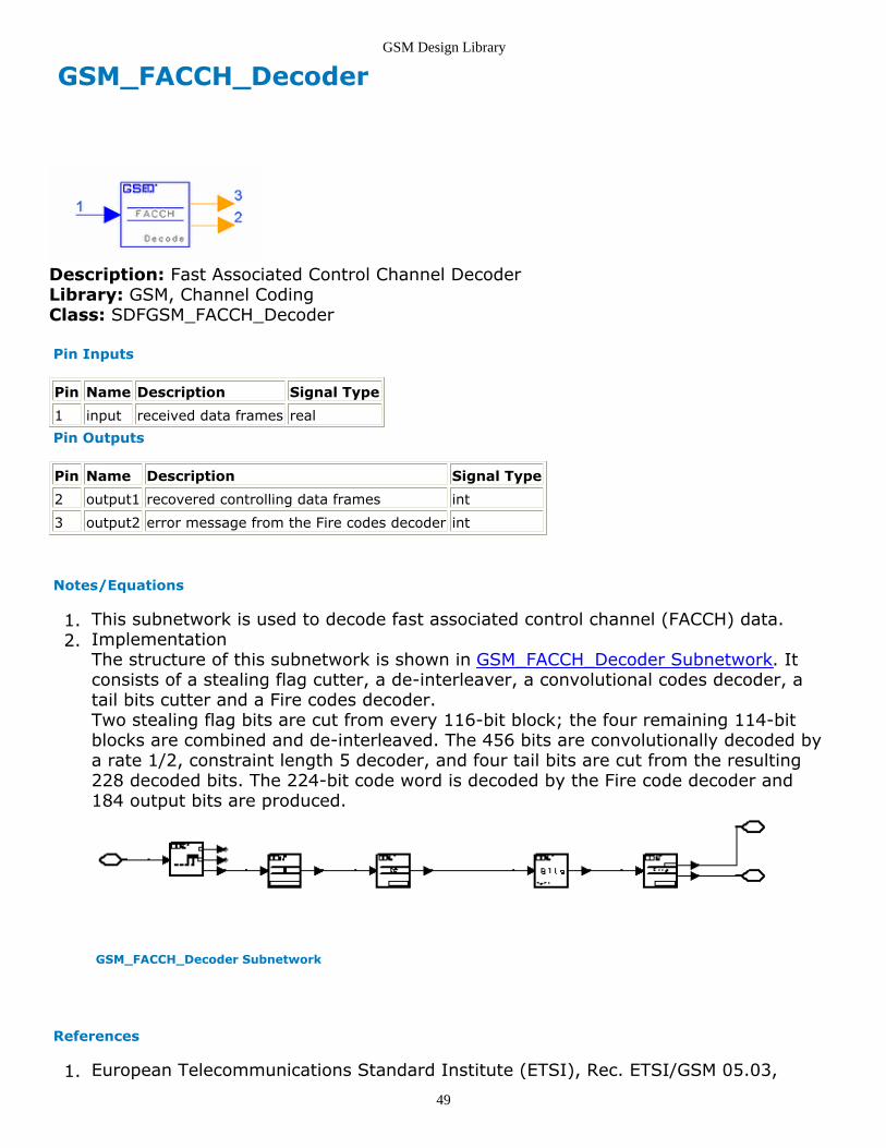
GSM_FACCH_Decoder
Description: Fast Associated Control Channel DecoderLibrary: GSM, Channel CodingClass: SDFGSM_FACCH_Decoder
Pin Inputs
Pin Name Description Signal Type
1 input received data frames real
Pin Outputs
Pin Name Description Signal Type
2 output1 recovered controlling data frames int
3 output2 error message from the Fire codes decoder int
Notes/Equations
This subnetwork is used to decode fast associated control channel (FACCH) data.1.Implementation2.The structure of this subnetwork is shown in GSM_FACCH_Decoder Subnetwork. Itconsists of a stealing flag cutter, a de-interleaver, a convolutional codes decoder, atail bits cutter and a Fire codes decoder.Two stealing flag bits are cut from every 116-bit block; the four remaining 114-bitblocks are combined and de-interleaved. The 456 bits are convolutionally decoded bya rate 1/2, constraint length 5 decoder, and four tail bits are cut from the resulting228 decoded bits. The 224-bit code word is decoded by the Fire code decoder and184 output bits are produced.
GSM_FACCH_Decoder Subnetwork
References
European Telecommunications Standard Institute (ETSI), Rec. ETSI/GSM 05.03,1.

GSM Design Library
50
Channel Coding, version 5.1.0, May 1996.

GSM Design Library
51

GSM Design Library
52
GSM_FACCH_Encoder
Description: Fast Associated Control Channel EncoderLibrary: GSM, Channel CodingClass: SDFGSM_FACCH_Encoder
Pin Inputs
Pin Name Description Signal Type
1 input controlling data frames of FACCH int
Pin Outputs
Pin Name Description Signal Type
2 output channel encoded data sequences int
Notes/Equations
This subnetwork is used to encode fast associated control channel (FACCH) data.1.Implementation2.The structure of this subnetwork is shown in GSM_FACCH_Encoder Subnetwork. Itincludes a cyclic codes encoder (implementing Fire codes encoding), a tail bitsinserter, a convolutional codes encoder and an interleaver. Each 184-bit input blockis cyclically encoded to form a 224-bit code word and four tail bits are inserted to theend of the code word. The 228-bit data block is encoded by a rate 1/2, constraintlength 5 convolutional codes encoder. The output 456-bit code word is block diagonalinterleaved and two stealing flags are inserted.
GSM_FACCH_Encoder Subnetwork
References

GSM Design Library
53
European Telecommunications Standard Institute (ETSI), Rec. ETSI/GSM 05.03,1.Channel Coding, version 3.5.1, March 1992.

GSM Design Library
54

GSM Design Library
55
GSM_FireDecoder
Description: Fire Code DecoderLibrary: GSM, Channel CodingClass: SDFGSM_FireDecoder
Parameters
Name Description Default Symbol Unit Type Range
ShortenFlag flag to indicate shortened code: NotShortened Code, Shortened Code
Not ShortenedCode
enum
GSM_CCH_Flag flag to indicate control channel code:General Fire Codes Decoder, Fire CodesDecoder for GSM CCH
Fire CodesDecoder forGSM CCH
enum †
N length of code word 279 n int (0, ∞) ††
K length of information part in code word 265 k int (0:N)N-(2L-1)-K=order ofg1(D)
Gen1 select g1(D), one of two generatorpolynomials of Fire code, in octal form: g145, g1 13, g1 400011
g1 45 enum
L one of the parameters of a Fire code, andthe other generator polynomial is g2(D) =D^(2*L-1) + 1
5 l int (0:(N-K+1)/2)†††
SS number of bits shortened in a code word(used only when ShortenFlag=ShortenedCode)
0 ss int (0, ∞)
† If GSM_CCH_Flag=Fire Codes Decoder for GSM CCH, all other parameters will not beused.†† N must also satisfy:(DN+1) must be divisible by g(D) when ShortenFlag=Not Shortened Code, or(D(N+SS)+1) must be divisible by g(D) when ShortenFlag=Shortened Code,where g(D) is the generator polynomial generated by g1(D) and g2(D), and g1(D) isspecified by Gen1, g2(D) = D(2L-1)+1.††† N+SS (when ShortenFlag=Shortened Code) orN (when ShortenFlag=Not Shortened Code)must equal LCM(2L-1, period), where period is the generator polynomial g1(D) period.
Pin Inputs

GSM Design Library
56
Pin Name Description Signal Type
1 input received code word int
Pin Outputs
Pin Name Description Signal Type
2 output decoded information block int
3 errMsg the message indicating error that cannot be corrected int
Notes/Equations
This model is used to decode Fire coded data.1.K output tokens are produced for each N input token consumed.
References
European Telecommunications Standard Institute (ETSI), Rec. ETSI/GSM 05.03,1.Channel Coding, version 5.1.0, May 1996.S. Lin and D. J. Costello, Jr., Error Control Coding Fundamentals and Applications,2.Prentice Hall, Englewood Cliffs NJ, 1983.

GSM Design Library
57

GSM Design Library
58
GSM_Interleaver_4
Description: Block Rectangular InterleaverLibrary: GSM, Channel CodingClass: SDFGSM_Interleaver_4
Parameters
Name Description Default Unit Type Range
CheckBit check input bits option: Check and stop at error, Check andwarn the error, No Checking
Check and stop aterror
enum
Pin Inputs
Pin Name Description Signal Type
1 input input data, one 456-bit block int
2 chType channel type, should be 1 here int
Pin Outputs
Pin Name Description Signal Type
3 output interleaved data and stealing flags, four 116-bit sub-blocks int
Notes/Equations
This model is used to interleave the input data in a block rectangular manner.1.464 output tokens are produced for each 456 input tokens consumed at pin input andone token is consumed at pin chType.Implementation2.The interleaving rule is:
where c(n, k) is the kth bit in the nth 456-bit coded data block, N marks a certaindata block, i(B, j) is the jth bit in the Bth 114-bit interleaved sub-block, and B 0 is the
initial value of B. The block of coded data is block rectangular interleaved, that is, anew data block starts every 4th block and is distributed over 4 blocks. Two stealingflags hu(B) and hl(B) are inserted into each block after interleaving. The flags shouldbe equal to 1 here to indicate control channels. In coding implementation, a presettable is used in converting the index k to the index j.

GSM Design Library
59
References
European Telecommunications Standard Institute (ETSI), Rec. ETSI/GSM 05.03,1.Channel Coding, version 5.1.0, May 1996.

GSM Design Library
60

GSM Design Library
61
GSM_Interleaver_8
Description: Block Diagonal InterleaverLibrary: GSM, Channel CodingClass: SDFGSM_Interleaver_8
Parameters
Name Description Default Unit Type Range
CheckBit check input bits option: Check and stop at error, Check andwarn the error, No Checking
Check and stop aterror
enum
Pin Inputs
Pin Name Description Signal Type
1 input input data, one 456-bit block int
2 chType channel type, 0 for TCH/FS, TCH/F2.4 and 1 for FACCH int
Pin Outputs
Pin Name Description Signal Type
3 output interleaved data and stealing flags, four 116-bit sub-blocks int
Notes/Equations
This model is used to interleave input data in a block diagonal manner.1.464 output tokens are produced for each 456 input tokens consumed at pin input andone token is consumed at pin chType.Implementation2.The interleaving rule is:
where c(n, k) is the kth bit in the nth 456-bit coded data block, N marks a certaindata block, i(B, j) is the jth bit in the Bth 114-bit interleaved sub-block, and B 0 is the
initial value of B. Stealing flags hu(B) and hl(B) are inserted into each block afterinterleaving; the flags are 0 for TCH/FS or TCH/F2. 4 and 1 for FACCH.In codingimplementation, a preset table is used to convert index k to index j.

GSM Design Library
62
References
European Telecommunications Standard Institute (ETSI), Rec. ETSI/GSM 05.03,1.Channel Coding, version 5.1.0, May 1996.

GSM Design Library
63

GSM Design Library
64
GSM_Interleaver_F96
Description: Diagonal InterleaverLibrary: GSM, Channel CodingClass: SDFGSM_Interleaver_F96
Parameters
Name Description Default Unit Type Range
CheckBit check input bits option: Check and stop at error, Check andwarn the error, No Checking
Check and stop aterror
enum
Pin Inputs
Pin Name Description Signal Type
1 input input data, 114-bit data block int
2 chType channel type (must be 0 here to indicate data traffic channel) int
Pin Outputs
Pin Name Description Signal Type
3 output interleaved data block and two stealing flags, 116-bit block int
Notes/Equations
This model is used to interleave the input data in a diagonal manner.1.116 output tokens are produced for each 114 input tokens consumed at pin input andone token consumed at pin chType.Implementation2.The interleaving rule is:
where c(n, k) is the kth bit in the nth 456-bit coded data block, N marks a certaindata block, i(B, j) is the jth bit in the Bth 114-bit interleaved sub-block, and B 0 is the
initial value of B. By dividing the 456-bit data block into four 114-bit blocks, we can

GSM Design Library
65
change the rule to
where is the index of the new blocks. Stealing flags hu(B) and hl(B) are inserted into eachblock after interleaving. The flags must be 0 to indicate traffic channels. In codingimplementation, a preset table is used in converting index k to index j. Theinterleaver output will have a 114×19 token delay.
References
European Telecommunications Standard Institute (ETSI), Rec. ETSI/GSM 05.03,1.Channel Coding, version 5.1.0, May 1996.

GSM Design Library
66

GSM Design Library
67
GSM_InverseReord
Description: TCH/FS Inverse ReorderLibrary: GSM, Channel CodingClass: SDFGSM_InverseReord
Parameters
Name Description Default Unit Type Range
CheckBit check input bits option: Check and stop at error, Check andwarn the error, No Checking
Check and stop aterror
enum
Pin Inputs
Pin Name Description Signal Type
1 input reordered data int
Pin Outputs
Pin Name Description Signal Type
2 cls1a class 1a bits and 3 parity bits int
3 cls1b class 1b bits int
Notes/Equations
This model is used to invert the reordering on the information and parity bits of1.TCH/FS frames.53 output tokens at cls1a and 132 output tokens at cls1b are produced for each 185input tokens consumed.Implementation2.The inverse reordering rule is:
where d(k), k = 0, 1, ... , 181 are the bits of class 1, p(k), k = 0, 1, 2 are the paritybits of the class 1a bits, and u(k), k = 0, 1, ... , 184 are the reordered bits.
References
European Telecommunications Standard Institute (ETSI), Rec. ETSI/GSM 05.03,1.Channel Coding, version 5.1.0, May 1996.

GSM Design Library
68

GSM Design Library
69
GSM_Puncture
Description: Data PunctureLibrary: GSM, Channel CodingClass: SDFGSM_Puncture
Pin Inputs
Pin Name Description Signal Type
1 input convolutionally encoded symbols. int
Pin Outputs
Pin Name Description Signal Type
2 output punctured Convolutionally encoded symbols. int
Notes/Equations
This model is used to puncture the input stream to implement punctured1.convolutional code for GSM data channel. 456 output tokens are produced when 488input tokens consumed.
References
European Telecommunications Standard Institute (ETSI), Rec. ETSI/GSM 05.03,1.Channel Coding, version 5.1.0, May 1996.

GSM Design Library
70

GSM Design Library
71
GSM_RACH_Decoder
Description: Random Access Channel DecoderLibrary: GSM, Channel CodingClass: SDFGSM_RACH_Decoder
Pin Inputs
Pin Name Description Signal Type
1 input1 received data frames real
2 input2 base station identity codes int
Pin Outputs
Pin Name Description Signal Type
3 output1 recovered controlling data frames int
4 output2 error message from the Fire codes decoder int
Notes/Equations
This subnetwork is used to decode random access channel data.1.Implementation2.The structure of this subnetwork is shown in GSM_RACH_Decoder Subnetwork. Itconsists of a convolutional codes decoder, a tail bits cutter, base station identitycodes (BSIC) adder, and a cyclic codes decoder. The input 36-bit block isconvolutionally decoded by a rate 1/2, constraint length 5 decoder, and four tail bitsare cut from the resulting 18 bits. In the remaining 14 bits, there are six color bitsthat are masked with the 6 BSIC bits to produce six parity check bits. These paritycheck bits and the other eight information bits are cyclically decoded and eightoutput bits are produced.
GSM_RACH_Decoder Subnetwork

GSM Design Library
72
References
European Telecommunications Standard Institute (ETSI), Rec. ETSI/GSM 05.03,1.Channel Coding, version 3.5.1, March 1992.

GSM Design Library
73

GSM Design Library
74
GSM_RACH_Encoder
Description: Random Access Channel EncoderLibrary: GSM, Channel CodingClass: SDFGSM_RACH_Encoder
Pin Inputs
Pin Name Description Signal Type
1 input1 controlling random access channel data frames int
2 input2 base station identity codes int
Pin Outputs
Pin Name Description Signal Type
3 output channel encoded data sequences int
Notes/Equations
This subnetwork is used to encode random access channel data.1.Implementation2.The structure of this subnetwork is shown in GSM_RACH_Encoder Subnetwork. Itconsists of a cyclic codes encoder, a BSIC (Base Station Identity Codes) adder, a tailbits inserter, and a convolutional codes encoder. Every 8-bit input block is cyclicallyencoded to form a 14-bit code word, and the six parity check bits in it are maskedwith 6 BSIC bits, result in 6 color bits. Then four tail bits are inserted to the end ofthe code word. Finally the 18-bit block is encoded by a rate 1/2, constraint length 5convolutional codes encoder, and produce 36 output bits.
GSM_RACH_Encoder Subnetwork
References

GSM Design Library
75
European Telecommunications Standard Institute (ETSI), Rec. ETSI/GSM 05.03,1.Channel Coding, version3.5.1, March 1992.

GSM Design Library
76

GSM Design Library
77
GSM_Reorder
Description: TCH/FS ReorderLibrary: GSM, Channel CodingClass: SDFGSM_Reorder
Parameters
Name Description Default Unit Type Range
CheckBit check input bits option: Check and stop at error, Check andwarn the error, No Checking
Check and stop aterror
enum
Pin Inputs
Pin Name Description Signal Type
1 cls1a cyclic encoded class 1a bits and 3 parity bits int
2 cls1b class 1b bits int
Pin Outputs
Pin Name Description Signal Type
3 out reordered data int
Notes/Equations
This model is used to reorder the information and parity bits of TCH/FS frames.1.185 output tokens are produced, 53 input tokens are consumed at the cls1a pin and132 input tokens are consumed at the cls1b pin.Implementation2.The reordering rule is:
where d(k), k=0, 1, ... , 181 are the bits of class 1, p(k), k=0, 1, 2 are the parity bitsof the class 1a bits, and u (k), k=0, 1, ... , 184 are the reordered bits.
References
European Telecommunications Standard Institute (ETSI), Rec. ETSI/GSM 05.03,1.Channel Coding, version 5.1.0, May 1996.

GSM Design Library
78

GSM Design Library
79
GSM_RmvStlFlgs
Description: Remove Stealing FlagsLibrary: GSM, Channel CodingClass: SDFGSM_RmvStlFlgs
Pin Inputs
Pin Name Description Signal Type
1 input 116-bit data block of normal burst real
Pin Outputs
Pin Name Description Signal Type
2 output 114-bit information block without stealing flags real
3 hl stealing flag hl(B) = e(B,57): odd-numbered bits in the 114-bit block real
4 hu stealing flag hu(B) = e(B,58): even numbered bits in the 114-bit block real
Notes/Equations
This model removes the two stealing flags from the burst before de-interleaving. 1441.output, 1 hl and 1 hu tokens are produced for each 116 input tokens consumed.Implementation2.Upper layer models will select an appropriate de-interleaving scheme using thestealing flags. The stealing flags are hl(B) and hu(B), where B is the index of the datablock. Assume d(B, k), B = 0, 1, ... , k = 0, 1, ... , 115, are the bits in block B, thenhl(B) = d(B, 57) and hu(B) = d(B, 58).
References
European Telecommunications Standard Institute (ETSI), Rec. ETSI/GSM 05.03,1.Channel Coding, version 5.1.0, May 1996.

GSM Design Library
80

GSM Design Library
81
GSM_SACCH_Decoder
Description: Slow Associated Control Channel DecoderLibrary: GSM, Channel CodingClass: SDFGSM_SACCH_Decoder
Pin Inputs
Pin Name Description Signal Type
1 input received data frames real
Pin Outputs
Pin Name Description Signal Type
2 output1 recovered controlling data frames int
3 output2 error message from the Fire codes decoder int
Notes/Equations
This subnetwork is used to decode slow associated control channel data.1.Implementation2.The structure of this subnetwork is shown in GSM_SACCH_Decoder Subnetwork. Itconsists of a stealing flag cutter, a de-interleaver, a convolutional codes decoder, atail bits cutter and a Fire codes decoder.
Two stealing flag bits are cut from every 116-bit block. Four remaining 114-bit blocks arecombined together and de-interleaved. Then the 456 bits are convolutionally decoded by arate 1/2, constraint length 5 decoder, and four tail bits are cut from the resulting 228decoded bits. Finally the 224-bit codeword is decoded by the Fire code decoder and 184output bits are produced.
GSM_SACCH_Decoder Subnetwork
References

GSM Design Library
82
European Telecommunications Standard Institute (ETSI), Rec. ETSI/GSM 05.03,1.Channel Coding, version 3.5.1, March 1992.

GSM Design Library
83

GSM Design Library
84
GSM_SACCH_Encoder
Description: Slow Associated Control Channel EncoderLibrary: GSM, Channel CodingClass: SDFGSM_SACCH_Encoder
Pin Inputs
Pin Name Description Signal Type
1 input controlling data frames of slow associated control channel int
Pin Outputs
Pin Name Description Signal Type
2 output channel encoded data sequences int
Notes/Equations
This subnetwork is used to encode slow associated control channel data.1.Implementation2.The structure of this subnetwork is shown in GSM_SACCH_Encoder Subnetwork. Itconsists of a cyclic codes encoder (implementing Fire codes encoding), a tail bitsinserter, a convolutional codes encoder and an interleaver. Every 184-bit input blockis cyclically encoded to form a 224-bit codeword and four tail bits are inserted to theend of the codeword. Then the 228-bit data block is encoded by a rate 1/2,constraint length 5 convolutional codes encoder, and the output 456-bit codeword isdivided into four 114-bit sub-blocks. Finally the interleaver interleaves these sub-blocks in a "block rectangular" way and inserts two stealing flags in them.
GSM_SACCH_Encoder Subnetwork

GSM Design Library
85
References
European Telecommunications Standard Institute (ETSI), Rec. ETSI/GSM 05.03,1.Channel Coding, version 3.5.1, March 1992.

GSM Design Library
86

GSM Design Library
87
GSM_SCH_Decoder
Description: Synchronization Channel DecoderLibrary: GSM, Channel CodingClass: SDFGSM_SCH_Decoder
Pin Inputs
Pin Name Description Signal Type
1 input received data frames real
Pin Outputs
Pin Name Description Signal Type
2 output1 recovered controlling data frames int
3 output2 error message from cyclic codes decoder int
Notes/Equations
This subnetwork is used to decode synchronization channel data.1.Implementation2.The structure of this subnetwork is shown in GSM_SCH_Decoder Subnetwork. Itconsists of a convolutional codes decoder, a tail bits cutter and a cyclic codesdecoder. A 78-bit input block is convolutionally decoded by the rate 1/2, constraintlength 5 decoder, and four tail bits are cut from the resulting 39 decoded bits. The35-bit codeword is further decoded by the cyclic codes decoder and 25 output bitsare produced.
GSM_SCH_Decoder Subnetwork
References
European Telecommunications Standard Institute (ETSI), Rec. ETSI/GSM 05.03,1.Channel Coding, version 5.1.0, May 1996.

GSM Design Library
88

GSM Design Library
89
GSM_SCH_Encoder
Description: Synchronization Channel EncoderLibrary: GSM, Channel CodingClass: SDFGSM_SCH_Encoder
Pin Inputs
Pin Name Description Signal Type
1 input controlling data frames of SCH int
Pin Outputs
Pin Name Description Signal Type
2 output channel encoded data sequences int
Notes/Equations
This subnetwork is used to encode synchronization channel (SCH) data.1.Implementation2.The structure of this subnetwork is shown in GSM_SCH_Encoder Subnetwork. Itconsists of a cyclic codes encoder, a tail bits inserter and a convolutional codesencoder. Each 25-bit input block is cyclically encoded to form a 35-bit codeword andfour tail bits are inserted to the end of the codeword. The 39-bit data block isencoded by a rate 1/2, constraint length 5 convolutional codes encoder and 78output bits are produced.
GSM_SCH_Encoder Subnetwork
References
European Telecommunications Standard Institute (ETSI), Rec. ETSI/GSM 05.03,1.Channel Coding, version 5.1.0, May 1996.

GSM Design Library
90

GSM Design Library
91
GSM_Splitter
Description: Split Input Block into Two Output BlocksLibrary: GSM, Channel CodingClass: SDFGSM_Splitter
Parameters
Name Description Default Unit Type Range
N1 block length of first output 182 int (0, ∞)
N2 block length of second output 78 int (0, ∞)
Pin Inputs
Pin Name Description Signal Type
1 in input data real
Pin Outputs
Pin Name Description Signal Type
2 out1 first of two outputs real
3 out2 second of two outputs real
Notes/Equations
This model is used to split the input block into two output blocks. It is used in TCH/FS1.to separate class 1 and class 2 bits, or class 1a bits (the first 50 bits of class 1) andclass 1b bits (the bits of class 1 other than class 1a bits in the speech frame). Eachfiring, N1 output tokens at out1 and N2 tokens at out2 are produced for each N1+N2input tokens consumed.
References
European Telecommunications Standard Institute (ETSI), Rec. ETSI/GSM 05.03,1.Channel Coding, version 5.1.0, May 1996.

GSM Design Library
92

GSM Design Library
93
GSM_TailBits
Description: Add or Remove Tailing BitsLibrary: GSM, Channel CodingClass: SDFGSM_TailBits
Parameters
Name Description Default Unit Type Range
AddRmvSwitch tailing bits option: Adding, Removing Adding enum
CheckBit check input bits option: Check and stop at error, Checkand warn the error, No Checking
Check and stopat error
enum
N number of tailing bits in a frame 4 int (0, ∞)
InfoLen number of information bits in a frame 185 int (0, ∞)
Pin Inputs
Pin Name Description Signal Type
1 input input frame int
Pin Outputs
Pin Name Description Signal Type
2 output output frame int
Notes/Equations
This model is used to add tailing bits to or remove tailing bits from the input frames.1.N+InfoLen output tokens are produced for each InfoLen input token consumed whenAddRmvSwitch=Adding; InfoLen output tokens are produced for each N+InfoLeninput token consumed when AddRmvSwitch=Removing.Implementation2.When AddRmvSwitch=Adding, N tailing bits are added after each InfoLen informationbits; when AddRmvSwitch=Removing, N tailing bits are removed from eachN+InfoLen input bits.
References
European Telecommunications Standard Institute (ETSI), Rec. ETSI/GSM 05.03,1.Channel Coding, version 5.1.0, May 1996.

GSM Design Library
94

GSM Design Library
95
GSM_TCHF24_Decoder
Description: TCH/F2.4 Channel DecoderLibrary: GSM, Channel CodingClass: SDFGSM_TCHF24_Decoder
Pin Inputs
Pin Name Description Signal Type
1 input received data frames real
Pin Outputs
Pin Name Description Signal Type
2 output recovered data frames int
Notes/Equations
This subnetwork is used to decode full rate traffic channel (2.4kbit/s) (TCH/F2.4)1.data.Implementation2.This subnetwork is shown in GSM_TCHF24_Decoder Subnetwork. It consists of astealing flag cutter, a de-interleaver, a convolutional codes decoder and a tail bitscutter. Two stealing flag bits are cut from every 116-bit block. Four remaining 114-bit blocks are combined and de-interleaved. The 456 bits are convolutionally decodedby a rate 1/6, constraint length 5 decoder. Four tail bits are cut from the resulting 76decoded bits.
GSM_TCHF24_Decoder Subnetwork
References
European Telecommunications Standard Institute (ETSI), Rec. ETSI/GSM 05.03,1.Channel Coding, version 5.1.0, May 1996.

GSM Design Library
96

GSM Design Library
97
GSM_TCHF24_Encoder
Description: TCH/F2.4 Channel EncoderLibrary: GSM, Channel CodingClass: SDFGSM_TCHF24_Encoder
Pin Inputs
Pin Name Description Signal Type
1 input data frames of TCH/F2.4 int
Pin Outputs
Pin Name Description Signal Type
2 output channel encoded data sequences int
Notes/Equations
This subnetwork is used to encode full rate traffic channel (2.4 kbit/s) (TCH/F2.4)1.data.Implementation2.This subnetwork is shown in GSM_TCHF24_Encoder Subnetwork. It consists of a tailbits inserter, a convolutional codes encoder, and an interleaver. Four tail bits areinserted into each 72 input information bits. These 76 bits are convolutionally codedin rate 1/6, constraint length 5 encoder and interleaved in a block diagonal manner.
GSM_TCHF24_Encoder Subnetwork
References

GSM Design Library
98
European Telecommunications Standard Institute (ETSI), Rec. ETSI/GSM 05.03,1.Channel Coding, version 5.1.0, May 1996.

GSM Design Library
99

GSM Design Library
100
GSM_TCHF48_Decoder
Description: TCH/F4.8 Channel DecoderLibrary: GSM, Channel CodingClass: SDFGSM_TCHF48_Decoder
Pin Inputs
Pin Name Description Signal Type
1 input received data frames real
Pin Outputs
Pin Name Description Signal Type
2 output recovered data frames int
Notes/Equations
This subnetwork is used to decode full rate traffic channel (4.8kbit/s) (TCH/F4.8)1.data.Implementation2.The subnetwork structure is shown in GSM_TCHF48_Decoder Subnetwork. It consistsof a stealing flag cutter, a de-interleaver, a convolutional codes decoder, and a tailbits cutter. Two stealing flag bits are cut from each 116-bit block; the remaining 114-bit block is de-interleaved in a diagonal manner. A delay of 228 bits is inserted tokeep the bit index consistent. Four 114-bit de-interleaved blocks are combined andconvolutionally decoded by a rate 1/3, constraint length 5 decoder. Four tail bits arecut from each 19 bits.
GSM_TCHF48_Decoder Subnetwork
References
European Telecommunications Standard Institute (ETSI), Rec. ETSI/GSM 05.03,1.Channel Coding, version 5.1.0, May 1996.

GSM Design Library
101

GSM Design Library
102
GSM_TCHF48_Encoder
Description: TCH/F4.8 Channel EncoderLibrary: GSM, Channel CodingClass: SDFGSM_TCHF48_Encoder
Pin Inputs
Pin Name Description Signal Type
1 input data frames of TCH/F4.8 int
Pin Outputs
Pin Name Description Signal Type
2 output channel encoded data sequences int
Notes/Equations
This subnetwork is used to encode full rate traffic channel (4.8 kbits) (TCH/F4.8)1.data.Implementation2.This subnetwork is shown in GSM_TCHF48_Encoder Subnetwork. It consists of a tailbits inserter, a convolutional codes encoder and an interleaver. Four tail bits areinserted into each 15 input information bits. 8(15+4)=152 bits are convolutionallyencoded by a rate 1/3, constraint length 5 encoder, and interleaved in a diagonalmanner.
GSM_TCHF48_Encoder Subnetwork

GSM Design Library
103
References
European Telecommunications Standard Institute (ETSI), Rec. ETSI/GSM 05.03,1.Channel Coding, version 5.1.0, May 1996.

GSM Design Library
104

GSM Design Library
105
GSM_TCHF96_Decoder
Description: TCH/F9.6 Channel DecoderLibrary: GSM, Channel CodingClass: SDFGSM_TCHF96_Decoder
Pin Inputs
Pin Name Description Signal Type
1 input received data frames real
Pin Outputs
Pin Name Description Signal Type
2 output recovered data frames int
Notes/Equations
This subnetwork is used to decode full rate traffic channel (9.6 kbits) (TCH/F9.6)1.data.Implementation2.This subnetwork structure is shown in GSM_TCHF96_Decoder Subnetwork. It consistsof a stealing flag cutter, a de-interleaver, a delayer, a de-puncturer, a convolutionalcodes decoder, and a tail bits cutter. Two stealing flag bits are cut from each 116-bitblock; the remaining 114-bit block is de-interleaved in a diagonal manner. A delay of228 bits is inserted to keep the bit index consistent. Four 114-bit de-interleavedblocks are combined, de-punctured and convolutionally decoded by a rate 1/2,constraint length 5 decoder. Four tail bits are cut from every 244 bits.
GSM_TCHF96_Decoder Subnetwork
References
European Telecommunications Standard Institute (ETSI), Rec. ETSI/GSM 05.03,1.Channel Coding, version 5.1.0, May 1996.

GSM Design Library
106

GSM Design Library
107
GSM_TCHF96_Encoder
Description: TCH/F9.6 Channel EncoderLibrary: GSM, Channel CodingClass: SDFGSM_TCHF96_Encoder
Pin Inputs
Pin Name Description Signal Type
1 input data frames of TCH/F9.6 int
Pin Outputs
Pin Name Description Signal Type
2 output channel encoded data sequences int
Notes/Equations
This subnetwork is used to encode full rate traffic channel (9.6kbit/s) (TCH/F9.6)1.data.Implementation2.This subnetwork structure is shown in GSM_TCHF96_Encoder Subnetwork. It consistsof a tail bits inserter, a convolutional codes encoder, a puncturer, and an interleaver.Four tail bits are inserted into each 240 input information bits; these 244 bits areconvolutionally encoded in rate 1/2, constraint length of 5 encoder, uniformlypunctured, and interleaved in a diagonal manner.
GSM_TCHF96_Encoder Subnetwork
References

GSM Design Library
108
European Telecommunications Standard Institute (ETSI), Rec. ETSI/GSM 05.03,1.Channel Coding, version 5.1.0, May 1996.

GSM Design Library
109

GSM Design Library
110
GSM_TCHFS_Decoder
Description: TCH/FS Channel DecoderLibrary: GSM, Channel CodingClass: SDFGSM_TCHFS_Decoder
Pin Inputs
Pin Name Description Signal Type
1 input received data frames real
Pin Outputs
Pin Name Description Signal Type
2 output1 output int
3 output2 error message from the cyclic codes decoder int
Notes/Equations
This subnetwork is used to decode full rate traffic channel (TCH/FS) data.1.Implementation2.This subnetwork is shown in GSM_TCHFS_Decoder Subnetwork. It includes a stealingflag cutter, a de-interleaver, a splitter, a convolutional codes decoder, a tail bitscutter, an inverse reorderer, a cyclic codes decoder and two combiners.TCH/FS Codec Data Flow shows the data flow of this subnetwork (refer toGSM_TCHFS_Encoder also).
GSM_TCHFS_Decoder Subnetwork

GSM Design Library
111
TCH/FS Codec Data Flow
References
European Telecommunications Standard Institute (ETSI), Rec. ETSI/GSM 05.03,1.Channel Coding, version 5.1.0, May 1996.

GSM Design Library
112

GSM Design Library
113
GSM_TCHFS_Encoder
Description: TCH/FS Channel EncoderLibrary: GSM, Channel CodingClass: SDFGSM_TCHFS_Encoder
Pin Inputs
Pin Name Description Signal Type
1 input controlling data frames int
Pin Outputs
Pin Name Description Signal Type
2 output channel encoded data sequences int
Notes/Equations
This subnetwork is used to encode full rate traffic channel (TCH/FS) data.1.Implementation2.This subnetwork structure is shown in GSM_TCHFS_Encoder Subnetwork. It includestwo splitters, a cyclic codes encoder, reorderer, a tail bits inserter, convolutionalcodes encoder, a combiner, and an interleaver. As shown in TCH/FS Codec Data Flow, data is split by two splitters: 1a is cyclically encoded; 1b (132 bits) is not cyclicallyencoded. The combined 1a and 1b are the most critical bits that use half-rateconvolutional coding after tail bits are added. Combined with the 78 bits of class 2,the channel coding subnetwork outputs a 456-bit data block.
GSM_TCHFS_Encoder Subnetwork

GSM Design Library
114
TCH/FS Codec Data Flow
References
European Telecommunications Standard Institute (ETSI), Rec. ETSI/GSM 05.03,1.Channel Coding, version 5.1.0, May 1996.

GSM Design Library
115
Equalization Components for GSMDesign Library
GSM ChannelEstimator (gsm)GSM Derotator (gsm)GSM Equalizer (gsm)GSM EquCombiner (gsm)GSM EquComposeAB (gsm)GSM EquDecomposeAB (gsm)GSM EquSplitter (gsm)GSM Filter (gsm)GSM Receiver (gsm)GSM ReceiverAB (gsm)

GSM Design Library
116

GSM Design Library
117
GSM_ChannelEstimator
Description: Channel Estimator Used in GSM Channel EqualizationLibrary: GSM, EqualizationClass: SDFGSM_ChannelEstimator
Parameters
Name Description Default Unit Type Range
Direction direction of estimation: Forward, Backward Forward enum
BurstType burst type: Normal Burst, Synchronization Burst, AccessBurst
NormalBurst
enum
L maximum delay of channel, in bit duration units, Tb 5 int [1:MAX_L]†
† MAX_L, typically lt_equal.gif 5, is defined in {_}EquHeader.h</em>
Pin Inputs
Pin Name Description Signal Type
1 input synchronized and derotated data complex
2 tsc training sequence code, defined by GSM 05.02 int
Pin Outputs
Pin Name Description Signal Type
3 output estimate of complex channel impluse response complex
4 index index used to correct synchronization int
Notes/Equations
This model is used to estimate the impulse response of the equivalent channel, which1.includes the effect of modulation and derotation. L+1 output tokens are produced atpin output and one token is produced at pin index for each N input tokens consumedat pin input and one token consumed at pin tsc, where N is frame length (see FrameLength N Value).
Frame Length N Value

GSM Design Library
118
N BurstType
87 + 2 × L Normal Burst
106 + 2 × L Synchronization Burst
80 + 2 × L Access Burst
References
R. Steele, Mobile Radio Communications, London: Pentech Press, 1992.1.European Telecommunications Standard Institute (ETSI), Rec. ETSI/GSM 05.02,2.Multiplexing and Multiple Access on the Radio Path, version 4.8.0, Nov. 1996.

GSM Design Library
119

GSM Design Library
120
GSM_Derotator
Description: Derotator Used in EqualizationLibrary: GSM, EqualizationClass: SDFGSM_Derotator
Pin Inputs
Pin Name Description Signal Type
1 input input data sequence complex
Pin Outputs
Pin Name Description Signal Type
2 output output data sequence complex
Notes/Equations/References
This model is used to derotate the received GMSK signals to compensate for rotation1.introduced by GMSK modulation. 156 output tokens are produced for each 156 inputtokens consumed at the input.Implementation2.The GMSK modulation introduces a rotation in the signal phase- the π/2 increase ordecrease of the phase in each bit duration. Removing this phase rotation before thematched filter can simplify subsequent processes.

GSM Design Library
121

GSM Design Library
122
GSM_Equalizer
Description: Adaptive Channel Equalizer with Matched FilterLibrary: GSM, EqualizationClass: SDFGSM_Equalizer
Parameters
Name Description Default Symbol Unit Type Range
BurstType burst type: Normal Burst, SynchronizationBurst, Access Burst
NormalBurst
enum
L maximum delay of channel in unit of Tb,the bit duration
5 int [1:MAX_L] †
TrackingFlag tracking option: Not Tracking, Tracking NotTracking
enum
TrackingStart start position of tracking 26 int [L:frameLength-L)††
S_Step step-size gain used in adjusting s, theequivalent channel coefficients
0.0 s real [0, ∞)
G_Step step-size gain used in adjusting g, thematched filter taps
0.0 g real [0, ∞)
† MAX_L, typically 5, is defined in EquHeader.h†† frameLength = 87 + 2L if BurstType = Normal BurstframeLength = 106 + 2L if BurstType = Synchronization BurstframeLength = 80+ 2L if BurstType = Access Burst
Pin Inputs
Pin Name Description Signal Type
1 input derotated signal, one sample per bit complex
2 index index used to correctsynchronization
int
3 chnl estimate of complex channel complex
Pin Outputs
Pin Name Description Signal Type
4 output equalized data real
Notes/Equations
This model is used to adaptively equalize received data. N output tokens are

GSM Design Library
123
1.produced at pin output for each N input token consumed at pin input, L+1 inputtokens consumed at pin chnl and one token consumed at pin index, where N is framelength (see Frame Length N Value).
Frame Length N Value
N BurstType
87 + 2 × L Normal Burst
106 + 2 ×L
Synchronization Burst
80 + 2 × L Access Burst
Implementation2.This model includes a matched filter and a Viterbi processor.The matched filter is used before the Viterbi processor to establish an optimumsignal-to-noise ratio. The number of taps of the matched filter is (L+1). In trainingmode, the matched filter gets its tap coefficients from GSM_ChannelEstimator, whichare the complex conjugates of the reverse sequence of the estimated channelimpulse response coefficients. In tracking mode, the matched filter establishes anoptimum signal-to-noise ratio of its output signals, while adjusting its tap gainsadaptively by a gradient algorithm.The Viterbi processor uses a modified Viterbi algorithm [1] that operates directly onthe matched filter output without whitening the noise.If TrackingFlag is set to Tracking, the entire sequence is equalized without tracking,then equalized again using the tracking algorithm and the results of the firstequalization. From this, the tracking performance band can be obtained.The index input is used on the results of the Viterbi processor to further correct thesynchronization. The results are output from the offset of the value of index andzeros are added to the end.
References
G. Ungerboeck, Adaptive maximum-likelihood receiver for carrier-modulated data-1.transmission system, IEEE Trans. Commun., vol. COM-22, pp. 624-636, May 1974.R. D'Avella, L. Moreno, M. Sant'Agostion, An adaptive MLSE receiver for TDMA digital2.mobile radio, IEEE Jour. on SAC, vol. 7, No. 1, pp. 122-129, Jan 1989.P. Qinhua, G. Yong, L. Weidong, Synchronization design theory of demodulation for3.digital land mobile radio system, Jour. of Beijing University of Posts andTelecommunications, vol. 18, No. 2, pp. 14-21, Jun 1995.

GSM Design Library
124

GSM Design Library
125
GSM_EquCombiner
Description: Combiner Used in Bidirectional EqualizationLibrary: GSM, EqualizationClass: SDFGSM_EquCombiner
Parameters
Name Description Default Unit Type Range
BurstType burst type: Normal Burst, Synchronization Burst Normal Burst enum
L maximum delay of channel in unit of Tb, the bit duration 5 int [1:MAX_L] †
† MAX_L, typically 5, is defined in EquHeader.h
Pin Inputs
Pin Name Description Signal Type
1 fwd forward frame real
2 bkwd backward frame real
Pin Outputs
Pin Name Description Signal Type
3 output combined burst real
Notes/Equations
This model is used to combine two input frames to a burst.1.156 output tokens are produced for each N input token consumed at pins fwd andbkwd, where N is frame length given in Value of frame length N.
Value of frame length N
N BurstType
87 + 2 × L Normal Burst
106 + 2 × L Synchronization Burst
Implementation2.Two input frames are combined to form a burst. Bidirectional Equalization for NormalBurst shows the split of a normal burst. Implementation of the synchronization burstis the same except for the length of training sequence, which is 64 bits.The forwardframe starts from the beginning of the training sequence and ends at the end of theburst; the backward frame starts from the end of the training sequence and ends at

GSM Design Library
126
the beginning of the burst. Since both frames contain a training sequence, only oneof the training sequences (Bidirectional Equalization for Normal Burst shows theforward frame) is embedded in the resulting burst. 8 bits of 0 are added to the endas guard bits to form a normal burst.
Bidirectional Equalization for Normal Burst
References
European Telecommunications Standard Institute (ETSI), Rec. ETSI/GSM 05.02,1.Multiplexing and Multiple Access on the Radio Path, version 4.8.0, Nov. 1996.

GSM Design Library
127

GSM Design Library
128
GSM_EquComposeAB
Description: Burst Composer of Access Burst in EqualizationLibrary: GSM, EqualizationClass: SDFGSM_EquComposeAB
Parameters
Name Description Default Unit Type Range
L maximum delay of channel in unit of Tb, the bit duration 5 int [1:MAX_L] †
† MAX_L, typically 5, is defined in EquHeader.h
Pin Inputs
Pin Name Description Signal Type
1 input equalized synchronizaiton and information sequence real
Pin Outputs
Pin Name Description Signal Type
2 output output burst real
Notes/Equations
This model is used to compose the Access Burst in equalization. 156 output tokens1.are produced for each 80+2×L input tokens are consumed at pin input.Implementation2.The structure of Access Burst is shown in Access Burst Structure. There are eightextended tail bits, a synchronization sequence, an information sequence, three tailbits equal to 0 and an extended guard sequence. The extended tail bits,synchronization sequence and the extended guard sequence are defined in reference[1]; the information sequence is defined in reference [2]. This model receives thesynchronization and information sequences with tail bits considering the spread ofthe channel and the matched filter, and composes the resulting burst by addingextended tail bits and filling the guard period with not return to zero signal 1, whichis mapping to the logical signal 0.

GSM Design Library
129
Access Burst Structure
References
European Telecommunications Standard Institute (ETSI), Rec. ETSI/GSM 05.02,1.Multiplexing and Multiple Access on the Radio Path, version 4.8.0, Nov. 1996.European Telecommunications Standard Institute (ETSI), Rec. ETSI/GSM 05.03,2.Channel Coding, version 5.1.0, May 1996.

GSM Design Library
130

GSM Design Library
131
GSM_EquDecomposeAB
Description: Burst Decomposer of Access Burst in EqualizationLibrary: GSM, EqualizationClass: SDFGSM_EquDecomposeAB
Parameters
Name Description Default Unit Type Range
L maximum delay of channel in unit of Tb, the bit duration 5 int [1:MAX_L] †
† MAX_L, typically 5, is defined in EquHeader.h
Pin Inputs
Pin Name Description Signal Type
1 input input burst complex
Pin Outputs
Pin Name Description Signal Type
2 output output synchronization and information sequence complex
Notes/Equations
This model is used to decompose the Access Burst in equalization. 80+2×L output1.tokens are produced for each 156 input tokens consumed at pin input.Implementation2.The structure of Access Burst is shown as Access Burst Structure. There are eightextended tail bits, a synchronization sequence, an information sequence, three tailbits equal to 0 and an extended guard sequence. The extended tail bits,synchronization sequence and the extended guard sequence are defined in reference[1]; the information sequence is defined in reference [2]. This model receives thewhole bit synchronized and derotated burst, and outputs the synchronization andinformation sequences with tail bits considering the spread of the channel and thematched filter.

GSM Design Library
132
Access Burst Structure
References
European Telecommunications Standard Institute (ETSI), Rec. ETSI/GSM 05.02,1.Multiplexing and Multiple Access on the Radio Path, version 4.8.0, Nov. 1996.European Telecommunications Standard Institute (ETSI), Rec. ETSI/GSM 05.03,2.Channel Coding, version 5.1.0, May 1996.

GSM Design Library
133

GSM Design Library
134
GSM_EquSplitter
Description: Splitter Used in Bidirectional EqualizationLibrary: GSM, EqualizationClass: SDFGSM_EquSplitter
Parameters
Name Description Default Unit Type Range
BurstType burst type: Normal Burst, Synchronization Burst Normal Burst enum
L Mmaximum delay of channel in unit of Tb, the bit duration 5 int [1:MAX_L] †
† MAX_L, typically 5, is defined in EquHeader.h
Pin Inputs
Pin Name Description Signal Type
1 input input burst complex
Pin Outputs
Pin Name Description Signal Type
2 fwd forward frame complex
3 bkwd backward frame complex
Notes/Equations
This model is used to split one burst into two frames. For each 156 input tokens are1.consumed at pin input, N output tokens at the fwd and bkwd pins are produced,where N is frame length (refer to Value of Frame Length N).
Value of Frame Length N
N BurstType
87 + 2 × L Normal Burst
106 + 2 × L Synchronization Burst
Implementation2.This model splits one burst into two frames, as shown in Bidirectional Equalizationand Normal Burst. The forward burst starts from the beginning of the trainingsequence and ends at the end of the burst; the backward burst starts at the end ofthe training sequence and ends at the beginning of the burst. Zeros are added toeach frame to reserve space for spreading signals introduced by the following

GSM Design Library
135
matched filter. The number of zeros is determined by parameter L, the maximumdelay of the channel. By considering the spreading of signals transmitted through thechannel, backward equalization starts at the Lth bit following the end of trainingsequence in the implementation of this component. Bidirectional Equalization andNormal Burst shows the split of a normal burst; implementation of a synchronizationburst is the same except for the length of the training sequence, which is 64 bits.
Bidirectional Equalization and Normal Burst
References
European Telecommunications Standard Institute (ETSI), Rec. ETSI/GSM 05.02,1.Multiplexing and Multiple Access on the Radio Path, version 4.8.0, Nov. 1996.

GSM Design Library
136

GSM Design Library
137
GSM_Filter
Description: 7-Pole Chebychev FilterLibrary: GSM, EqualizationClass: SDFGSM_Filter
Pin Inputs
Pin Name Description Signal Type
1 input modulated signal that has passed through the channel real
Pin Outputs
Pin Name Description Signal Type
2 output filtered baseband signal real
Notes/Equations
This subnetwork is a 7-pole Chebychev filter that is used as a baseband filter in the1.GSM receiver.Implementation2.This subnetwork is designed by Digital Filter Designer of Agilent's Advanced DesignSystem. The 3 dB bandwidth is 100 kHz. GSM_Filter Subnetwork shows thesubnetwork structure.
GSM_Filter Subnetwork
References
S. M. Redl, Matthias, M. W. Oliphant, An Introduction To GSM, Artech House1.Publishers, 1995.

GSM Design Library
138

GSM Design Library
139
GSM_Receiver
Description: Adaptive MLSE ReceiverLibrary: GSM, EqualizationClass: SDFGSM_Receiver
Parameters
Name Description Default Symbol Unit Type Range
TSC training sequence code 0 int [0:7]
BurstType burst type: Normal Burst, SynchronizationBurst
NormalBurst
enum
L maximum delay of channel in unit of Tb,the bit duration
5 int [1:MAX_L] †
TrackingFlag tracking option: Not Tracking, Tracking NotTracking
enum
TrackingStart start position of tracking 26 int [L:frameLength-L)††
S_Step step-size gain used in adjusting s, theequivalent channel coefficients
0.0 s real [0, ∞)
G_Step step-size gain used in adjusting g, thematched filter taps
0.0 g real [0, ∞)
† MAX_L, typically 5, is defined in EquHeader.h†† if BurstType=Normal Burst, frameLength=87+2Lif BurstType=Synchronization Burst, frameLength=106+2L.
Pin Inputs
Pin Name Description Signal Type
1 input input data sequence complex
Pin Outputs
Pin Name Description Signal Type
2 output combined burst real
Notes/Equations
This subnetwork is used to restore the data sequence from the received and1.synchronized signals.Implementation2.The construction of this subnetwork is shown in Viterbi Adaptive Receiver BlockDiagram.

GSM Design Library
140
is the received signals samples, one sample per bit.
is the equalized data.The input data is derotated to demodulate GMSK modulation. It is split into a forwardand a backward subframe in reverse order for the training sequence that is in themiddle of the input frame. Both subframes are weighted with the channel estimatesobtained using the training sequence and equalized with a modified Viterbi algorithm.The equalized subframes are then combined into one frame.
Viterbi Adaptive Receiver Block Diagram
References
European Telecommunications Standard Institute (ETSI), Rec. ETSI/GSM 05.03,1.Channel Coding, version 5.1.0, May 1996.R. Steele, Mobile Radio Communications, London: Pentech Press, 1992.2.European Telecommunications Standard Institute (ETSI), Rec. ETSI/GSM 05.02,3.Multiplexing and Multiple Access on the Radio Path, version 4.8.0, Nov. 1996.G. Ungerboeck, Adaptive maximum-likelihood receiver for carrier-modulated data-4.transmission system, IEEE Trans. Commun., vol. COM-22, May 1974, pp. 624-636.R. D'Avella, L. Moreno, M. Sant'Agostion, An adaptive MLSE receiver for TDMA digital5.mobile radio, IEEE J. Select. Areas Commun., vol. 7, Jan. 1989, pp. 122-129 .

GSM Design Library
141

GSM Design Library
142
GSM_ReceiverAB
Description: Adaptive MLSE Receiver for Access BurstLibrary: GSM, EqualizationClass: SDFGSM_ReceiverAB
Parameters
Name Description Default Unit Type Range
L maximum delay of channel in unit of Tb, the bit duration 5 int [1:MAX_L] †
† MAX_L, typically 5, is defined in EquHeader.h
Pin Inputs
Pin Name Description Signal Type
1 input input data sequence complex
Pin Outputs
Pin Name Description Signal Type
2 output combined burst real
Notes/Equations
This subnetwork is used to restore the data sequence from the received and1.synchronized signals of access burst.Implementation2.The construction of this subnetwork is shown in Viterbi Adaptive Receiver for AccessBurst Block Diagram.
is the received signals samples, one sample per bit.
is the equalized data.Input data is split into synchronization and information sequences after de-rotation.The synchronization sequence is used for calculating channel estimates with whichthe information sequence is equalized. The synchronization and equalized informationsequences are combined.

GSM Design Library
143
Viterbi Adaptive Receiver for Access Burst Block Diagram
References
European Telecommunications Standard Institute (ETSI), Rec. ETSI/GSM 05.03,1.Channel Coding, version 5.1.0, May 1996.R. Steele, Mobile Radio Communications, London: Pentech Press, 1992.2.European Telecommunications Standard Institute (ETSI), Rec. ETSI/GSM 05.02,3.Multiplexing and Multiple Access on the Radio Path, version 4.8.0, Nov. 1996.G. Ungerboeck, Adaptive maximum-likelihood receiver for carrier-modulated data-4.transmission system, IEEE Trans. Commun., vol. COM-22, May 1974, pp. 624-636.R. D'Avella, L. Moreno, M. Sant'Agostion, An adaptive MLSE receiver for TDMA digital5.mobile radio, IEEE J. Select. Areas Commun., vol. 7, Jan. 1989, pp. 122-129.

GSM Design Library
144
Framing Components for GSM DesignLibrary
GSM AccessBurst (gsm)GSM BcchCcch4SdcchDn (gsm)GSM BcchCcch4SdcchUp (gsm)GSM BcchCcchDn (gsm)GSM BcchCcchUp (gsm)GSM DeAccessBurst (gsm)GSM DeBcchCcch4SdcchDn (gsm)GSM DeBcchCcch4SdcchUp (gsm)GSM DeBcchCcchDn (gsm)GSM DeMultiframe26 (gsm)GSM DeNormalBurst (gsm)GSM DeSBurst (gsm)GSM DeSdcch8Dn (gsm)GSM DeSdcch8Up (gsm)GSM DeTDMA (gsm)GSM DummyBurst (gsm)GSM FBurst (gsm)GSM Multiframe26 (gsm)GSM NormalBurst (gsm)GSM SBurst (gsm)GSM Sdcch8Dn (gsm)GSM Sdcch8Up (gsm)GSM TDMA (gsm)GSM TimeBaseCounter (gsm)

GSM Design Library
145

GSM Design Library
146
GSM_AccessBurst
Description: Access Burst ConstructionLibrary: GSM, FramingClass: SDFGSM_AccessBurst
Pin Inputs
Pin Name Description Signal Type
1 input 36 encrypted bits int
Pin Outputs
Pin Name Description Signal Type
2 output 156 modulating bits including 8-bit guarding period int
Notes/Equations
This model is used to construct an access burst of 156 bits defined in GSM standard1.05.02.156 output tokens are produced for each 36 encrypted tokens consumed.Implementation2.Access Burst Structure shows the access burst structure. The synchronizationsequence is defined as(BN8,BN9, ... , BN48) =(0,1,0,0,1,0,1,1,0,1,1,1,1,1,1,1,1,0,0,1,1,0,0,1,1,0,1,0,1,0,1,0,0,0, 1,1,1,1,0,0,0)
Access Burst Structure
References
European Telecommunications Standard Institute (ETSI), Rec. ETSI/GSM 05.02,1.Multiplexing and Multiple Access on the Radio Path, version 3.5.1, March 1992.

GSM Design Library
147

GSM Design Library
148
GSM_BcchCcch4SdcchDn
Description: BCCH+CCCH+4SDCCH Downlink ConstructionLibrary: GSM, FramingClass: SDFGSM_BcchCcch4SdcchDn
Pin Inputs
Pin Name Description Signal Type
1 SCH SCH Signal int
2 BCCH BCCH Signal int
3 CCCH CCCH signal int
4 SACCH SACCH signal int
5 SDCCH SDCCH Signal int
Pin Outputs
Pin Name Description Signal Type
6 output 51-frame multiframe of BCCH+CCCH+4SDCCH downlink int
Notes/Equations
This model is used to construct a BCCH+CCCH+4SDCCH downlink 51-frame1.multiframe as defined in GSM 05.02 standard.51×8×156 output tokens are produced for each input set of tokens consumed.SCH: 4×8×156 tokens are consumed each firing.BCCH: 4×8×156 tokens are consumed each firing.CCCH: 12×8×156 tokens are consumed each firing.SACCH: 8×8×156 tokens are consumed each firing.SDCCH: 16×8×156 tokens are consumed each firing.Implementation2.BCCH+CCCH+4 SDCCH/4 Downlink Structure shows the structure of a 51-framemultiframe BCCH+CCCH downlink.

GSM Design Library
149
BCCH+CCCH+4 SDCCH/4 Downlink Structure
References
European Telecommunications Standard Institute (ETSI), Rec. ETSI/GSM 05.02,1.Multiplexing and Multiple Access on the Radio Path, version 3.5.1, March 1992.

GSM Design Library
150

GSM Design Library
151
GSM_BcchCcch4SdcchUp
Description: BCCH+CCCH+4SDCCH Uplink ConstructionLibrary: GSM, FramingClass: SDFGSM_BcchCcch4SdcchUp
Pin Inputs
Pin Name Description Signal Type
1 RACH RACH signal int
2 SACCH SACCH signal int
3 SDCCH SDCCH signal int
Pin Outputs
Pin Name Description Signal Type
4 output 51-frame multiframe of BCCH+CCCH+4SDCCH uplink int
Notes/Equations
This model is used to construct a BCCH+CCCH+4 SDCCH/4 51-frame multiframe1.uplink as defined in GSM 05.02 standard.51×8×156 output tokens are produced for each input set of tokens consumed.RACH: 27×8×156 tokens are consumed each firing.SACCH: 8×156 tokens are consumed each firing.SDCCH: 16×8×156 tokens are consumed each firing.Implementation2.BCCH+CCCH+4SDCCH Uplink Structure shows a BCCH+CCCH+4 SDCCH/4 51-framemultiframe uplink structure.
BCCH+CCCH+4SDCCH Uplink Structure
References

GSM Design Library
152
European Telecommunications Standard Institute (ETSI), Rec. ETSI/GSM 05.02,1.Multiplexing and Multiple Access on the Radio Path, version 3.5.1, March 1992.European Telecommunications Standard Institute (ETSI), Rec. ETSI/GSM 03.03,2.Numbering, addressing and identification, version 3.5.1, March 1992.European Telecommunications Standard Institute (ETSI), Rec. ETSI/GSM 04.03,3.Mobile Station - Base Station System (MS - BSS) interface Channel structures andaccess capabilities, version 3.5.1, March 1992.

GSM Design Library
153

GSM Design Library
154
GSM_BcchCcchDn
Description: BCCH+CCCH Downlink ConstructionLibrary: GSM, FramingClass: SDFGSM_BcchCcchDn
Pin Inputs
Pin Name Description Signal Type
1 SCH SCH signal int
2 BCCH BCCH signal int
3 CCCH CCCH signal int
Pin Outputs
Pin Name Description Signal Type
4 output 51-frame multiframe of BCCH+CCCH downlink int
Notes/Equations
This model is used to construct a BCCH+CCCH downlink 51-frame multiframe as1.defined in GSM 05.02 standard.51×8×156 output tokens are produced for each input set of tokens consumed.SCH: 5×8×156 tokens are consumed each firing.BCCH: 4×8×156 tokens are consumed each firing.CCCH: 36×8×156 tokens are consumed each firing.Implementation2.BCCH+CCCH Downlink Structure shows structure of a 51-frame multiframeBCCH+CCCH downlink.
BCCH+CCCH Downlink Structure
References
European Telecommunications Standard Institute (ETSI), Rec. ETSI/GSM 05.02,1.

GSM Design Library
155
vMultiplexing and Multiple Access on the Radio Path_, version 3.5.1, March 1992.European Telecommunications Standard Institute (ETSI), Rec. ETSI/GSM 03.03,2.Numbering, addressing and identification, version 3.5.1, March 1992.European Telecommunications Standard Institute (ETSI), Rec. ETSI/GSM 04.03,3.Mobile Station - Base Station System (MS - BSS) interface Channel structures andaccess capabilities, version 3.5.1, March 1992.

GSM Design Library
156

GSM Design Library
157
GSM_BcchCcchUp
Description: BCCH+CCCH Uplink ConstructionLibrary: GSM, FramingClass: SDFGSM_BcchCcchUp
Pin Inputs
Pin Name Description Signal Type
1 input RACH signal int
Pin Outputs
Pin Name Description Signal Type
2 output 51-frame multiframe of BCCH+CCCH uplink int
Notes/Equations
This model is used to construct a BCCH+CCCH uplink 51-frame multiframe as defined1.in GSM 05.02 standard. One output token is produced for one input token consumed.Implementation2.BCCH+CCCH Uplink Structure shows structure of 51-frame multiframe BCCH+CCCHuplink.
BCCH+CCCH Uplink Structure
References
European Telecommunications Standard Institute (ETSI), Rec. ETSI/GSM 05.02,1.Multiplexing and Multiple Access on the Radio Path, version 3.5.1, March 1992.European Telecommunications Standard Institute (ETSI), Rec. ETSI/GSM 03.03,2.Numbering, addressing and identification, version 3.5.1, March 1992.European Telecommunications Standard Institute (ETSI), Rec. ETSI/GSM 04.03,3.Mobile Station - Base Station System (MS - BSS) interface Channel structures andaccess capabilities, version 3.5.1, March 1992.

GSM Design Library
158

GSM Design Library
159
GSM_DeAccessBurst
Description: Access Burst DisassemblyLibrary: GSM, FramingClass: SDFGSM_DeAccessBurst
Pin Inputs
Pin Name Description Signal Type
1 input 156 bits of access burst real
Pin Outputs
Pin Name Description Signal Type
2 output 36 encrypted bits real
Notes/Equations/References
This model is used to disassemble the access burst as defined in GSM 05.021.standard.36 output tokens are produced for each 156 tokens consumed.Implementation2.Access Burst Structure shows the access burst structure.
Access Burst Structure
References
European Telecommunications Standard Institute (ETSI), Rec. ETSI/GSM 05.02,1.Multiplexing and Multiple Access on the Radio Path, version 3.5.1, March 1992.European Telecommunications Standard Institute (ETSI), Rec. ETSI/GSM 03.03,2.Numbering, addressing and identification, version 3.5.1, March 1992.European Telecommunications Standard Institute (ETSI), Rec. ETSI/GSM 04.03,3.Mobile Station - Base Station System (MS - BSS) interface Channel structures andaccess capabilities, version 3.5.1, March 1992.

GSM Design Library
160

GSM Design Library
161
GSM_DeBcchCcch4SdcchDn
Description: BCCH+CCCH+4SDCCH Downlink DisassemblyLibrary: GSM, FramingClass: SDFGSM_DeBcchCcch4SdcchDn
Pin Inputs
Pin Name Description Signal Type
1 input 51-frame multiframe real
Pin Outputs
Pin Name Description Signal Type
2 SCH SCH signal real
3 BCCH BCCH signal real
4 CCCH CCCH signal real
5 SACCH SACCH signal real
6 SDCCH SDCCH signal real
Notes/Equations/References
This model is used to disassemble the BCCH+CCCH+4 SDCCH/4 downlink as defined1.in GSM 05.02 standard.51×8×156 input tokens are consumed each firing.SCH: 27×8×156 output tokens are produced for each input set of tokens consumed.BCCH: 4×8×156 output tokens are produced for each input set of tokens consumed.CCCH: 12×8×156 output tokens are produced for each input set of tokensconsumed.SACCH: 8×8×156 output tokens are produced for each input set of tokensconsumed.SDCCH: 16×8×156 output tokens are produced for each input set of tokensconsumed.Implementation2.BCCH+CCCH+4 SDCCH/4 Downlink Structure shows structure of 51-framemultiframe BCCH+CCCH+4SDCCH downlink.

GSM Design Library
162
BCCH+CCCH+4 SDCCH/4 Downlink Structure
References
European Telecommunications Standard Institute (ETSI), Rec. ETSI/GSM 05.02,1.Multiplexing and Multiple Access on the Radio Path, version 3.5.1, March 1992.European Telecommunications Standard Institute (ETSI), Rec. ETSI/GSM 03.03,2.Numbering, addressing and identification, version 3.5.1, March 1992.European Telecommunications Standard Institute (ETSI), Rec. ETSI/GSM 04.03,3.Mobile Station - Base Station System (MS - BSS) interface Channel structures andaccess capabilities, version 3.5.1, March 1992.

GSM Design Library
163

GSM Design Library
164
GSM_DeBcchCcch4SdcchUp
Description: BCCH+CCCH+4SDCCH Uplink DisassemblyLibrary: GSM, FramingClass: SDFGSM_DeBcchCcch4SdcchUp
Pin Inputs
Pin Name Description Signal Type
1 input 51-frame multifrmae real
Pin Outputs
Pin Name Description Signal Type
2 RACH RACH signal real
3 SACCH SACCH signal real
4 SDCCH SDCCH signal real
Notes/Equations
This model is used to disassemble the BCCH+CCCH+4 SDCCH/4 uplink as defined in1.GSM 05.02 standard.51×8×156 input tokens are consumed each firing.RACH: 27×8×156 output tokens are produced for each input set of tokensconsumed.SACCH: 8×8×156 output tokens are produced for each input set of tokensconsumed.SDCCH: 16×8×156 output tokens are produced for each input set of tokensconsumed.Implementation2.BCCH+CCCH+4SDCCH Uplink Structure shows structure of a 51-frame multiframeBCCH+CCCH +4SDCCH uplink.
BCCH+CCCH+4SDCCH Uplink Structure

GSM Design Library
165
References
European Telecommunications Standard Institute (ETSI), Rec. ETSI/GSM 05.02,1.Multiplexing and Multiple Access on the Radio Path, version 3.5.1, March 1992.European Telecommunications Standard Institute (ETSI), Rec. ETSI/GSM 03.03,2.Numbering, addressing and identification, version 3.5.1, March 1992.European Telecommunications Standard Institute (ETSI), Rec. ETSI/GSM 04.03,3.Mobile Station - Base Station System (MS - BSS) interface Channel structures andaccess capabilities, version 3.5.1, March 1992.

GSM Design Library
166

GSM Design Library
167
GSM_DeBcchCcchDn
Description: BCCH+CCCH Downlink DisassemblyLibrary: GSM, FramingClass: SDFGSM_DeBcchCcchDn
Pin Inputs
Pin Name Description Signal Type
1 input 51-frame multiframe real
Pin Outputs
Pin Name Description Signal Type
2 SCH SCH signal real
3 BCCH BCCH signal real
4 CCCH CCCH signal real
Notes/Equations
This model is used to disassemble a BCCH+CCCH downlink 51-frame multiframe as1.defined in GSM 05.02 standard.51×8×156 input tokens are consumed each firing.SCH: 5×8×156 output tokens are produced for each input set of tokens consumed.BCCH: 4×8×156 output tokens are produced for each input set of tokens consumed.CCCH: 36×8×156 output tokens are produced for each input set of tokensconsumed.Implementation2.BCCH+CCCH Downlink Structure shows structure of 51-frame multiframeBCCH+CCCH downlink.
BCCH+CCCH Downlink Structure
References

GSM Design Library
168
European Telecommunications Standard Institute (ETSI), Rec. ETSI/GSM 05.02,1.Multiplexing and Multiple Access on the Radio Path, version 3.5.1, March 1992.European Telecommunications Standard Institute (ETSI), Rec. ETSI/GSM 03.03,2.Numbering, addressing and identification, version 3.5.1, March 1992.European Telecommunications Standard Institute (ETSI), Rec. ETSI/GSM 04.03,3.Mobile Station - Base Station System (MS - BSS) interface Channel structures andaccess capabilities, version 3.5.1, March 1992.

GSM Design Library
169

GSM Design Library
170
GSM_DeMultiframe26
Description: 26-frame Multiframe DisassemblyLibrary: GSM, FramingClass: SDFGSM_DeMultiframe26
Pin Inputs
Pin Name Description Signal Type
1 input 26-frame mutiframe of 26*8*156 bits real
Pin Outputs
Pin Name Description Signal Type
2 TCH TCH signal real
3 SACCH SACCH signal real
Notes/Equations
This model is used to disassemble 26-frame multiframe as defined in GSM 05.021.standard.26×8×156 input tokens are consumed each firing.TCH: 24×8×156 output tokens are produced for each input set of tokens consumed.SACCH: 8×156 output tokens are produced for each input set of tokens consumed.Implementation2.26-Frame Multiframe TCH/FS Structure shows structure of 26-frame multiframeTCH/FS.
26-Frame Multiframe TCH/FS Structure
References
European Telecommunications Standard Institute (ETSI), Rec. ETSI/GSM 05.02,1.Multiplexing and Multiple Access on the Radio Path, version 3.5.1, March 1992.European Telecommunications Standard Institute (ETSI), Rec. ETSI/GSM 03.03,2.

GSM Design Library
171
Numbering, addressing and identification, version 3.5.1, March 1992.European Telecommunications Standard Institute (ETSI), Rec. ETSI/GSM 04.03,3.Mobile Station - Base Station System (MS - BSS) interface Channel structures andaccess capabilities, version 3.5.1, March 1992.

GSM Design Library
172

GSM Design Library
173
GSM_DeNormalBurst
Description: Normal Burst DisassemblyLibrary: GSM, FramingClass: SDFGSM_DeNormalBurst
Pin Inputs
Pin Name Description Signal Type
1 input 156 bits of normal burst real
Pin Outputs
Pin Name Description Signal Type
2 output 2*58 encrypted bits real
Notes/Equations
This model is used to disassemble the normal burst of 156 bits defined in GSM 05.021.standard.2×58 output tokens are produced for each 156 tokens consumed.Implementation2.Normal Burst Structure shows the normal burst structure.
Normal Burst Structure
References
European Telecommunications Standard Institute (ETSI), Rec. ETSI/GSM 05.02,1.Multiplexing and Multiple Access on the Radio Path, version 3.5.1, March 1992.European Telecommunications Standard Institute (ETSI), Rec. ETSI/GSM 03.03,2.Numbering, addressing and identification, version 3.5.1, March 1992.European Telecommunications Standard Institute (ETSI), Rec. ETSI/GSM 04.03,3.Mobile Station - Base Station System (MS - BSS) interface Channel structures andaccess capabilities, version 3.5.1, March 1992.

GSM Design Library
174

GSM Design Library
175
GSM_DeSBurst
Description: Synchronization Burst DisassemblyLibrary: GSM, FramingClass: SDFGSM_DeSBurst
Pin Inputs
Pin Name Description Signal Type
1 input synchronization burst bits real
Pin Outputs
Pin Name Description Signal Type
2 output encrypted bits real
Notes/Equations
This model is used to disassemble a synchronization burst of 156 bits as defined in1.GSM 05.02 standard.Each firing, 156 input tokens are consumed; 2×39 output tokens are produced foreach input set of tokens consumed.Implementation2.Synchronization Burst Structure shows the synchronization burst structure.
Synchronization Burst Structure
References
European Telecommunications Standard Institute (ETSI), Rec. ETSI/GSM 05.02,1.Multiplexing and Multiple Access on the Radio Path, version 3.5.1, March 1992.European Telecommunications Standard Institute (ETSI), Rec. ETSI/GSM 03.03,2.Numbering, addressing and identification, version 3.5.1, March 1992.European Telecommunications Standard Institute (ETSI), Rec. ETSI/GSM 04.03,3.Mobile Station - Base Station System (MS - BSS) interface Channel structures andaccess capabilities, version 3.5.1, March 1992.

GSM Design Library
176

GSM Design Library
177
GSM_DeSdcch8Dn
Description: 8SDCCH/8 Downlink DisassemblyLibrary: GSM, FramingClass: SDFGSM_DeSdcch8Dn
Pin Inputs
Pin Name Description Signal Type
1 input 51-frame multiframe of 51*8*156 bits real
Pin Outputs
Pin Name Description Signal Type
2 SACCH SACCH signal real
3 SDCCH SDCCH signal real
Notes/Equations
This model is used to disassemble an 8SDCCH/8 downlink 51-frame multiframe as1.defined in GSM 05.02 standard.51×8×156 input tokens are consumed each firing.SACCH: 16×8×156 output tokens are produced for each input set of tokensconsumed.SDCCH: 32×8×156 output tokens are produced for each input set of tokensconsumed.Implementation2.8SDCCH/8 Downlink Structure shows structure of 51-frame multiframe 8SDCCH/8downlink.
8SDCCH/8 Downlink Structure
References

GSM Design Library
178
European Telecommunications Standard Institute (ETSI), Rec. ETSI/GSM 05.02,1.Multiplexing and Multiple Access on the Radio Path, version 3.5.1, March 1992.European Telecommunications Standard Institute (ETSI), Rec. ETSI/GSM 03.03,2.Numbering, addressing and identification, version 3.5.1, March 1992.European Telecommunications Standard Institute (ETSI), Rec. ETSI/GSM 04.03,3.Mobile Station - Base Station System (MS - BSS) interface Channel structures andaccess capabilities, version 3.5.1, March 1992.

GSM Design Library
179

GSM Design Library
180
GSM_DeSdcch8Up
Description: 8SDCCH/8 Uplink DisassemblyLibrary: GSM, FramingClass: SDFGSM_DeSdcch8Up
Pin Inputs
Pin Name Description Signal Type
1 input 51-frame multiframe of 51*8*156 bits real
Pin Outputs
Pin Name Description Signal Type
2 SACCH SACCH signal real
3 SDCCH SDCCH signal real
Notes/Equations
This model is used to disassemble an 8SDCCH/8 uplink 51-frame multiframe as1.defined in GSM 05.02 standard.51×8×156 input tokens are consumed each firing.SACCH: 16×8×156 output tokens are produced for each input set of tokensconsumed.SDCCH: 32×8×156 output tokens are produced for each input set of tokensconsumed.Implementation2.8SDCCH/8 Uplink Structure shows structure of 51-frame multiframe 8SDCCH/8uplink.
8SDCCH/8 Uplink Structure
References

GSM Design Library
181
European Telecommunications Standard Institute (ETSI), Rec. ETSI/GSM 05.02,1.Multiplexing and Multiple Access on the Radio Path, version 3.5.1, March 1992.European Telecommunications Standard Institute (ETSI), Rec. ETSI/GSM 03.03,2.Numbering, addressing and identification, version 3.5.1, March 1992.European Telecommunications Standard Institute (ETSI), Rec. ETSI/GSM 04.03,3.Mobile Station - Base Station System (MS - BSS) interface Channel structures andaccess capabilities, version 3.5.1, March 1992.

GSM Design Library
182

GSM Design Library
183
GSM_DeTDMA
Description: TDMA Frame DisassemblyLibrary: GSM, FramingClass: SDFGSM_DeTDMA
Pin Inputs
Pin Name Description Signal Type
1 input one TDMA frame of eight time slots anytype
Pin Outputs
Pin Name Description Signal Type
2 O_TN7 data for time slot 7 anytype
3 O_TN6 data for time slot 6 anytype
4 O_TN5 data for time slot 5 anytype
5 O_TN4 data for time slot 4 anytype
6 O_TN3 data for time slot 3 anytype
7 O_TN2 data for time slot 2 anytype
8 O_TN1 data for time slot 1 anytype
9 O_TN0 data for time slot 0 anytype
Notes/Equations
This model is used to disassemble a TDMA frame into 8 time slots as defined in GSM1.05.02 standard.Implementation2.In GSM standard, one TDMA frame contains 8 time slots TN0 to TN7. The designerselects a time slot to fill with input data; the idle time slots will be filled with 0. Forexample, Time Slot Assignments shows TN2 and TN4 selected, the first 156 input bitsof the model will be placed in the third time slot, the second into the fifth, and theothers are filled with 0.GSM_DeTDMA Subnetwork shows the subnetwork structure, which consists ofBusMerge and Commutator.
Time Slot Assignments

GSM Design Library
184
GSM_DeTDMA Subnetwork
References
European Telecommunications Standard Institute (ETSI), Rec. ETSI/GSM 05.02,1.Multiplexing and Multiple Access on the Radio Path, version 3.5.1, March 1992.European Telecommunications Standard Institute (ETSI), Rec. ETSI/GSM 03.03,2.Numbering, addressing and identification, version 3.5.1, March 1992.European Telecommunications Standard Institute (ETSI), Rec. ETSI/GSM 04.03,3.Mobile Station - Base Station System (MS - BSS) interface Channel structures andaccess capabilities, version 3.5.1, March 1992.

GSM Design Library
185

GSM Design Library
186
GSM_DummyBurst
Description: Dummy Burst ConstructionLibrary: GSM, FramingClass: SDFGSM_DummyBurst
Pin Outputs
Pin Name Description Signal Type
1 output 156 modulating bits including 8-bit guarding period int
Notes/Equations
This model is used to construct dummy burst of 156 bits defined in GSM 05.021.standard.156 output tokens are produced.Implementation2.Dummy Burst Structure shows structure of dummy burst.
Dummy Burst Structure
References
European Telecommunications Standard Institute (ETSI), Rec. ETSI/GSM 05.02,1.Multiplexing and Multiple Access on the Radio Path, version 3.5.1, March 1992.European Telecommunications Standard Institute (ETSI), Rec. ETSI/GSM 03.03,2.Numbering, addressing and identification, version 3.5.1, March 1992.European Telecommunications Standard Institute (ETSI), Rec. ETSI/GSM 04.03,3.Mobile Station - Base Station System (MS - BSS) interface Channel structures andaccess capabilities, version 3.5.1, March 1992.

GSM Design Library
187

GSM Design Library
188
GSM_FBurst
Description: Frequency Correction Burst ConstructionLibrary: GSM, FramingClass: SDFGSM_FBurst
Pin Outputs
Pin Name Description Signal Type
1 output 156 modulating bits including 8-bit guarding period int
Notes/Equations
This model is used to construct frequency correction burst of 156 bits defined in GSM1.05.02 standard.156 output tokens are produced.Implementation2.Frequency Correction Burst Structure shows the frequency correction burst structure.Bits BN0 to BN2 and BN145 to BN147 are the tail bits; BN3 to BN144 are the fixedzero bits.
Frequency Correction Burst Structure
In the TDMA construction, the frequency correction burst must be assigned to timeslot 0.Frequency Correction Burst shows implementation of the model. After all 156 bits ofthe burst are arranged, the model outputs the burst as a block. The model consumesand produces data according to the specific bit number indicated in FrequencyCorrection Burst.

GSM Design Library
189
Frequency Correction Burst
References
European Telecommunications Standard Institute (ETSI), Rec. ETSI/GSM 05.02,1.Multiplexing and Multiple Access on the Radio Path, version 3.5.1, March 1992.European Telecommunications Standard Institute (ETSI), Rec. ETSI/GSM 03.03,2.Numbering, addressing and identification, version 3.5.1, March 1992.European Telecommunications Standard Institute (ETSI), Rec. ETSI/GSM 04.03,3.Mobile Station - Base Station System (MS - BSS) interface Channel structures andaccess capabilities, version 3.5.1, March 1992.

GSM Design Library
190

GSM Design Library
191
GSM_Multiframe26
Description: 26-frame Multiframe ConstructionLibrary: GSM, FramingClass: SDFGSM_Multiframe26
Pin Inputs
Pin Name Description Signal Type
1 TCH TCH signal int
2 SACCH SACCH signal int
Pin Outputs
Pin Name Description Signal Type
3 output 26-frame multiframe int
Notes/Equations
This model is used to construct 26-frame multiframe defined in GSM 05.02 standard.1.26×8×156 output tokens are produced each firing.TCH: 24×8×156 input tokens are consumed each firing.SACCH: 8×156 input tokens are consumed each firing.Implementation2.26-Frame Multiframe Structure shows the 26-multiframe structure. One 26-framemultiframe consists of 26 TDMA frames.
26-Frame Multiframe Structure
References
European Telecommunications Standard Institute (ETSI), Rec. ETSI/GSM 05.02,1.Multiplexing and Multiple Access on the Radio Path, version 3.5.1, March 1992.European Telecommunications Standard Institute (ETSI), Rec. ETSI/GSM 03.03,2.Numbering, addressing and identification, version 3.5.1, March 1992.

GSM Design Library
192
European Telecommunications Standard Institute (ETSI), Rec. ETSI/GSM 04.03,3.Mobile Station - Base Station System (MS - BSS) interface Channel structures andaccess capabilities, version 3.5.1, March 1992.

GSM Design Library
193

GSM Design Library
194
GSM_NormalBurst
Description: Normal Burst ConstructionLibrary: GSM, FramingClass: SDFGSM_NormalBurst
Parameters
Name Description Default Unit Type Range
TSC training sequence code, varies from 0 to 7. 0 int [0:7]
Pin Inputs
Pin Name Description Signal Type
1 input 2*58 information bits int
Pin Outputs
Pin Name Description Signal Type
2 output 156 modulating bits with 8-bit guarding period int
Notes/Equations
The model is used to construct a normal burst of 156 bits as defined in GSM 05.021.standard.156 output tokens are produced for each 2×58 tokens consumed.Implementation2.Normal Burst Structure shows the normal burst structure. Bits BN0 to BN2 andBN145 to BN147 are tail bits; BN3 to BN60 and BN87 to BN144 are encrypted bitsthat are outputs of channel coding models; BN61 to BN86 are training bits.8.25-bit periods must be added to each burst and presented with 0 bit in simulation.Bit representation is not available for the 0.25-bit; the 0.25-bit guarding time periodwill be added in modulation.
Normal Burst Structure
GSM defines eight different training sequences in normal burst, which are identifiedby training sequence code value. The following table shows the relation betweentraining sequence code and training sequence bits.

GSM Design Library
195
Training Sequence Code Training Sequence Bits
0 0,0,1,0,0,1,0,1,1,1,0,0,0,0,1,0,0,0,1,0,0,1,0,1,1,1
1 0,0,1,0,1,1,0,1,1,1,0,1,1,1,1,0,0,0,1,0,1,1,0,1,1,1
2 0,1,0,0,0,0,1,1,1,0,1,1,1,0,1,0,0,1,0,0,0,0,1,1,1,0
3 0,1,0,0,0,1,1,1,1,0,1,1,0,1,0,0,0,1,0,0,0,1,1,1,1,0
4 0,0,0,1,1,0,1,0,1,1,1,0,0,1,0,0,0,0,0,1,1,0,1,0,1,1
5 0,1,0,0,1,1,1,0,1,0,1,1,0,0,0,0,0,1,0,0,1,1,1,0,1,0
6 1,0,1,0,0,1,1,1,1,1,0,1,1,0,0,0,1,0,1,0,0,1,1,1,1,1
7 1,1,1,0,1,1,1,1,0,0,0,1,0,0,1,0,1,1,1,0,1,1,1,1,0,0
References
European Telecommunications Standard Institute (ETSI), Rec. ETSI/GSM 05.02,1.Multiplexing and Multiple Access on the Radio Path, version 3.5.1, March 1992.European Telecommunications Standard Institute (ETSI), Rec. ETSI/GSM 03.03,2.Numbering, addressing and identification, version 3.5.1, March 1992.GSM Recommendation 04.03, Mobile Station - Base Station System (MS - BSS)3.interface Channel structures and access capabilities, version 3.5.1, March 1992.

GSM Design Library
196

GSM Design Library
197
GSM_SBurst
Description: Synchronization Burst ConstructionLibrary: GSM, FramingClass: SDFGSM_SBurst
Pin Inputs
Pin Name Description Signal Type
1 input 2*39 encrypted bits int
Pin Outputs
Pin Name Description Signal Type
2 output 156 modulating bits including 8-bit guarding period int
Notes/Equations
The model is used to construct synchronization burst of 156 bits defined in GSM1.05.02 standard.156 output tokens are produced for each 2×39 tokens consumed.Implementation2.Synchronization Burst Structure shows the synchronization burst structure.
Synchronization Burst Structure
In the TDMA construction, the frequency correction burst must be assigned to timeslot 0.The extended training bits are defined as(BN42, BN43, ... , BN105)=(1,0,1,1,1,0,0,1,0,1,1,0,0,0,1,0,0,0,0,0,0,1,0,0,0,0,0,0,1,1,1,1,0,0,1,0,1,1,0,1,0,1,0,0,0,1,0,1,0,1,1,1,0,1,1,0,0,0,0,1,1,0,1,1)

GSM Design Library
198
References
European Telecommunications Standard Institute (ETSI), Rec. ETSI/GSM 05.02,1.Multiplexing and Multiple Access on the Radio Path, version 3.5.1, March 1992.European Telecommunications Standard Institute (ETSI), Rec. ETSI/GSM 03.03,2.Numbering, addressing and identification, version 3.5.1, March 1992.European Telecommunications Standard Institute (ETSI), Rec. ETSI/GSM 04.03,3.Mobile Station - Base Station System (MS - BSS) interface Channel structures andaccess capabilities, version 3.5.1, March 1992.

GSM Design Library
199

GSM Design Library
200
GSM_Sdcch8Dn
Description: 8SDCCH/8 Downlink ConstructionLibrary: GSM, FramingClass: SDFGSM_Sdcch8Dn
Pin Inputs
Pin Name Description Signal Type
1 SACCH SACCH signal int
2 SDCCH SDCCH signal int
Pin Outputs
Pin Name Description Signal Type
3 output 51-frame multiframe of SDCCH downlink int
Notes/Equations
This model is used to construct an 8SDCCH/8 downlink 51-frame multiframe as1.defined in GSM 05.02 standard.51×8×156 output tokens are produced for each input set of tokens consumed.SACCH: 16×8×156 input tokens are consumed each firing.SDCCH: 32×8×156 input tokens are consumed each firing.Implementation2.8SDCCH/8 Downlink Structure shows the 51-frame multiframe structure. One 51-frame multiframe consists of 51 TDMA frames. The expression SDCCH/8+SACCH/8indicates that eight different SDCCHs can be used with eight SACCH resources in thiscombination, and thus may serve for eight parallel signaling links on one physicalchannel.
8SDCCH/8 Downlink Structure

GSM Design Library
201
References
European Telecommunications Standard Institute (ETSI), Rec. ETSI/GSM 05.02,1.Multiplexing and Multiple Access on the Radio Path, version 3.5.1, March 1992.European Telecommunications Standard Institute (ETSI), Rec. ETSI/GSM 03.03,2.Numbering, addressing and identification, version 3.5.1, March 1992.European Telecommunications Standard Institute (ETSI), Rec. ETSI/GSM 04.03,3.Mobile Station - Base Station System (MS - BSS) interface Channel structures andaccess capabilities, version 3.5.1, March 1992.

GSM Design Library
202

GSM Design Library
203
GSM_Sdcch8Up
Description: 8SDCCH/8 Uplink ConstructionLibrary: GSM, FramingClass: SDFGSM_Sdcch8Up
Pin Inputs
Pin Name Description Signal Type
1 SACCH SACCH signal int
2 SDCCH SDCCH signal int
Pin Outputs
Pin Name Description Signal Type
3 output 51-frame multiframe of SDCCH uplink int
Notes/Equations
This model is used to construct an 8SDCCH/8 uplink 51-frame multiframe as defined1.in GSM 05.02 standard.51×8×156 output tokens are produced for each input set of tokens consumed.SACCH: 16×8×156 input tokens are consumed each firing.SDCCH: 32×8×156 input tokens are consumed each firing.Implementation2.8SDCCH/8 Uplink Structure shows structure of 51-frame multiframe 8SDCCH/8uplink.8SDCCH/8 Uplink Construction shows the implementation of the model. The modelconsumes and produces data according to the specific frame number indicated.
8SDCCH/8 Uplink Structure

GSM Design Library
204
8SDCCH/8 Uplink Construction
References
European Telecommunications Standard Institute (ETSI), Rec. ETSI/GSM 05.02,1.Multiplexing and Multiple Access on the Radio Path, version 3.5.1, March 1992.European Telecommunications Standard Institute (ETSI), Rec. ETSI/GSM 03.03,2.Numbering, addressing and identification, version 3.5.1, March 1992.European Telecommunications Standard Institute (ETSI), Rec. ETSI/GSM 04.03,3.Mobile Station - Base Station System (MS - BSS) interface Channel structures andaccess capabilities, version 3.5.1, March 1992.

GSM Design Library
205

GSM Design Library
206
GSM_TDMA
Description: TDMA Frame ConstructionLibrary: GSM, FramingClass: SDFGSM_TDMA
Pin Inputs
Pin Name Description Signal Type
1 TN7 data for time slot 7 anytype
2 TN6 data for time slot 6 anytype
3 TN5 data for time slot 5 anytype
4 TN4 data for time slot 4 anytype
5 TN3 data for time slot 3 anytype
6 TN2 data for time slot 2 anytype
7 TN1 data for time slot 1 anytype
8 TN0 data for time slot 0 anytype
Pin Outputs
Pin Name Description Signal Type
9 output one TDMA frame of consist of 8 time slots anytype
Notes/Equations
This subnetwork is used to construct one TDMA frame as defined in GSM 05.021.standard.Implementation2.In GSM standard, one TDMA frame contains eight time slots TN0 to TN7. Thedesigner selects which time slots to fill with input data; the idle time slots will befilled with 0. Time Slot Assignments shows TN2 and TN4 are selected, the first 156input bits of the subnetwork will be placed in the third time slot, the second into thefifth, the rest will be filled with 0.GSM_TDMA Subnetwork shows the structure of the subnetwork; it consists ofBusmerge and Commutator.
Time Slot Assignments

GSM Design Library
207
GSM_TDMA Subnetwork
References
European Telecommunications Standard Institute (ETSI), Rec. ETSI/GSM 05.02,1.Multiplexing and Multiple Access on the Radio Path, version 3.5.1, March 1992.European Telecommunications Standard Institute (ETSI), Rec. ETSI/GSM 03.03,2.Numbering, addressing and identification, version 3.5.1, March 1992.European Telecommunications Standard Institute (ETSI), Rec. ETSI/GSM 04.03,3.Mobile Station - Base Station System (MS - BSS) interface Channel structures andaccess capabilities, version 3.5.1, March 1992.

GSM Design Library
208

GSM Design Library
209
GSM_TimeBaseCounter
Description: Time Base Counter for T1, T2, T3Library: GSM, FramingClass: SDFGSM_TimeBaseCounter
Pin Inputs
Pin Name Description Signal Type
1 input modulating data int
Pin Outputs
Pin Name Description Signal Type
2 T1 counter for superframes int
3 T2 counter for frames in 26-frame multiframe structure int
4 T3 counter for frames in 51-frame multiframe structure int
Notes/Equations
This model is used to perform as GSM timebase counters for counting T1, T2, and T31.as defined in GSM 05.02 standard. One token of T1, T2, and T3 are produced foreach 8×156 input tokens consumed.Implementation2.When describing the signaling frame structure, it is important to know which frame iscurrently being transmitted. To remove the possibility of ambiguity: T1 counts thesuperframes; T2 counts frames in 26-frame multiframe structures; T3 counts thesignaling frames, which are 51-frame multiframe structures (T3 ranges from 0 to50).At starting time, the counters are set to 0, and the frames begin to be transmitted.When a speech or signaling multiframe structure is finished, its respective counters(T2 or T3) are reset to 0 and start again.After 1326 TDMA frames, T2 and T3 are reset and start counting again from 0. Thismarks the duration of one superframe. When the first superframe is completed, T1increments by 1. T1 only resets after 2047, which takes more than 3 hours to do so,and this is the duration of a hyperframe.
References
European Telecommunications Standard Institute (ETSI), Rec. ETSI/GSM 05.02,1.Multiplexing and Multiple Access on the Radio Path, version 3.5.1, March 1992.

GSM Design Library
210
European Telecommunications Standard Institute (ETSI), Rec. ETSI/GSM 03.03,2.Numbering, addressing and identification, version 3.5.1, March 1992.European Telecommunications Standard Institute (ETSI), Rec. ETSI/GSM 04.03,3.Mobile Station - Base Station System (MS - BSS) interface Channel structures andaccess capabilities, version 3.5.1, March 1992.

GSM Design Library
211
Measurement Components for GSMDesign Library
GSM BerFer (gsm)GSM ErrPatternDisplay (gsm)

GSM Design Library
212

GSM Design Library
213
GSM_BerFer
Description: Ber and Fer PerformanceLibrary: GSM, MeasurementClass: SDFGSM_BerFer
Parameters
Name Description Default Symbol Unit Type Range
Start frame from which measurement starts DefaultNumericStart F1 int [0:inf]
Stop frame at which measurement stops DefaultNumericStop F2 int [F1:inf]
FrameLength number of bits in a frame 1 N int [1:inf]
Pin Inputs
Pin Name Description Signal Type
1 in1 first expected or estimated sequence anytype
2 in2 second expected or estimated sequence anytype
Pin Outputs
Pin Name Description Signal Type
3 BE sum of bit errors from start of simulation int
4 BER output bit error rate real
5 FE sum of frame errors from start of simulation int
6 FER output frame error rate real
Notes/Equations
This model is used to calculate system bit error rate (BER) and frame error rate1.(FER). One output token is produced for each N token consumed.Implementation2.The Monte Carlo method is used to calculate the BER and FER of the system from theF1 th frame to the F2 th frame.

GSM Design Library
214

GSM Design Library
215
GSM_ErrPatternDisplay
Description: Error Pattern Display Used in EqualizationLibrary: GSM, MeasurementClass: SDFGSM_ErrPatternDisplay
Pin Inputs
Pin Name Description Signal Type
1 input1 first input data sequence to be compared real
2 input2 second input data sequence to be compared real
Pin Outputs
Pin Name Description Signal Type
3 pos position of each bit in burst to be used in x-axis real
4 output error ratio of each bit in burst real
Notes/Equations
This model is used to display error distribution in a burst. 148 output tokens are1.produced for each 156 input tokens consumed.Implementation2.This model compares the source bursts with the equalization results bit-by- bit, andaccumulates bit error numbers for each bit position in a burst. The error distributionin bursts can be obtained by using the position of each bit of burst as x-axis. Forevery burst of 156 bits, only the first 148 bits are considered; the eight guard bitsare ignored.

GSM Design Library
216
Modem ComponentsGSM AQuarterBitAdd (gsm)GSM AQuarterBitRmv (gsm)GSM Carrier (gsm)GSM DifferDecoder (gsm)GSM DifferEncoder (gsm)GSM GMSKDemod (gsm)GSM GMSKMod (gsm)GSM MpyClock (gsm)GSM Rom (gsm)

GSM Design Library
217

GSM Design Library
218
GSM_AQuarterBitAdd
Description: Add 0.25-Bit to 156-Bit BurstLibrary: GSM, ModemsClass: SDFGSM_AQuarterBitAdd
Parameters
Name Description Default Unit Type Range
SampleRate number of samples in one bit interval: SampleRate 4,SampleRate 8, SampleRate 16
SampleRate16
enum
Pin Inputs
Pin Name Description Signal Type
1 st modulated signal with a burst of 156 bits complex
2 fi carrier frequency real
Pin Outputs
Pin Name Description Signal Type
3 sa modulated signal with a burst of 156.25 bits complex
4 fo carrier frequency real
Notes/Equations
This model is used to add 0.25bit×M points that are set from 0 to a burst of 156 bits1.of modulated signal in order to simulate a burst of 156.25 bits in a GSM system.st: Input 156×Mfi: Input 156×Msa: Output 156.25×Mfo: Output 156.25×MImplementation2.Implementation of GSM_AQuarterBitAdd shows the implementation of the model.
Implementation of GSM_AQuarterBitAdd

GSM Design Library
219
References
European Telecommunications Standard Institute (ETSI), Rec. ETSI/GSM 05.01,1.Physical layer on the radio path; General description, version 5.0.0, May 1996.

GSM Design Library
220

GSM Design Library
221
GSM_AQuarterBitRmv
Description: Remove 0.25-Bit from 156.25-Bit BurstLibrary: GSM, ModemsClass: SDFGSM_AQuarterBitRmv
Parameters
Name Description Default Unit Type Range
SampleRate number of samples in one bit interval: SampleRate 4,SampleRate 8, SampleRate 16
SampleRate16
enum
Pin Inputs
Pin Name Description Signal Type
1 st modulated signal with a burst of 156.25 bits complex
2 fi carrier frequency real
Pin Outputs
Pin Name Description Signal Type
3 so modulated signal with a burst of 156 bits complex
4 fo carrier frequency real
Notes/Equations
This model is used to remove 0.25-bit×M points in a burst of 156.25-bit×M points of1.modulated signal. It is the reverse process of GSM_AQuarterBitAdd. After removal ofthe 0.25-bit, the signal will be sent to the demodulation model for demodulation.st: Input 156.25×Mfi: Input 156.25×Mso: Output 156×Mfo: Output 156×MImplementation2.Implementation of GSM_AQuarterBitRmv shows the implementation of the model.

GSM Design Library
222
Implementation of GSM_AQuarterBitRmv
References
European Telecommunications Standard Institute (ETSI), Rec. ETSI/GSM 05.01,1.Physical layer on the radio path; General description, version 5.0.0, May 1996.

GSM Design Library
223

GSM Design Library
224
GSM_Carrier
Description: Generation of Modulated SignalLibrary: GSM, ModemsClass: SDFGSM_Carrier
Parameters
Name Description Default Unit Type Range
Fc carrier frequency 45e6 Hz real (0, ∞)
Pc power per modulating bit 1e-3 W real (0, ∞)
Pin Inputs
Pin Name Description Signal Type
1 Ii COS value of the modulated signal phase real
2 Qi SIN value of the modulated signal phase real
Pin Outputs
Pin Name Description Signal Type
3 It I branch of complex envelope of modulated signal real
4 Qt Q branch of complex envelope of modulated signal real
5 fo carrier frequency real
Notes/Equations
This model is used to generate modulated signal which is represented by complex1.envelope equivalent and carrier frequency.One token is consumed at each input pin; one token is produced at each output pin.Implementation2.The modulated signal is:
where
is a random phase and is constant during one burst. In general, we set .
Then,

GSM Design Library
225
where
References
European Telecommunications Standard Institute (ETSI), Rec. ETSI/GSM 05.04,1.European Digital Cellular Telecommunications System, Modulation, version 4.0.3,Sept. 1994.

GSM Design Library
226

GSM Design Library
227
GSM_DifferDecoder
Description: Differential Decoder of Input BitsLibrary: GSM, ModemsClass: SDFGSM_DifferDecoder
Pin Inputs
Pin Name Description Signal Type
1 ak input bits, taking the value of 1 or -1 int
Pin Outputs
Pin Name Description Signal Type
2 ck differentially decoded bits, taking the value of 0 or 1 int
Notes/Equations
This model is used to implement differential decoding of the input bits to match the1.differential encoding of a GMSK signal. The initial value of the first bit is set to 1, thesame as differential encoding. One token is consumed at the input, one token isproduced at the output.Implementation2.GSM_DifferDecoder Implementation shows the implementation of the model.
GSM_DifferDecoder Implementation
References
European Telecommunications Standard Institute (ETSI), Rec. ETSI/GSM 05.04,1.European Digital Cellular Telecommunications System, Modulation, version 4.0.3,Sept. 1994.

GSM Design Library
228

GSM Design Library
229
GSM_DifferEncoder
Description: Differential Encoder of Input BitsLibrary: GSM, ModemsClass: SDFGSM_DifferEncoder
Pin Inputs
Pin Name Description Signal Type
1 dk input bits, taking the value of 0 or 1 int
Pin Outputs
Pin Name Description Signal Type
2 ak differentially encoded bits, taking the value of 1 or -1 int
Notes/Equations
This model is used to implement differential encoding of the input bits, which is1.required in GSM standard to generate GMSK signal. According to the standard GSM05.04, the initial value of the first bit is assigned to 1.One token is consumed at the input, one token is produced at the output.Implementation2.GSM_DifferEncoder Implementation shows the implementation of the model.
GSM_DifferEncoder Implementation
References
European Telecommunications Standard Institute (ETSI), Rec. ETSI/GSM 05.04,1.European Digital Cellular Telecommunications System, Modulation, version 4.0.3,Sept. 1994.

GSM Design Library
230

GSM Design Library
231
GSM_GMSKDemod
Description: Demodulation of GMSK Modulated SignaLibrary: Testing (for development use only)Class: SDFGSM_GMSKDemod
Pin Inputs
Pin Name Description Signal Type
1 input GMSK modulated data complex
Pin Outputs
Pin Name Description Signal Type
2 ck differentially decoded bits, taking the value of 0 or 1 int
Notes/Equations
This subnetwork is used to demodulate the GMSK modulated signal to recover the1.original bit stream.Implementation2.Two branches of modulated signal I and Q go through two quantizers to determine 1(when >0) or −1(when <0). After the two quantized signals are module-2 added, thesignal multiplies the reverse clock signal and is demodulated. Refer toGSM_GMSKDemod Block Diagram.
GSM_GMSKDemod Block Diagram

GSM Design Library
232
References
European Telecommunications Standard Institute (ETSI), Rec. ETSI/GSM 05.04,1.European Digital Cellular Telecommunications System, Modulation, version 4.0.3,Sept. 1994.

GSM Design Library
233

GSM Design Library
234
GSM_GMSKMod
Description: Generation of GMSK Modulated SignalLibrary: GSM, ModemsClass: SDFGSM_GMSKMod
Parameters
Name Description Default Unit Type Range
SampleRate number of samples in one bit interval: SampleRate 4,SampleRate 8, SampleRate 16
SampleRate16
enum
Fc carrier frequency 45e6 Hz real (0, ∞)
Pc power per modulating bit 1e-3 W real (0, ∞)
Pin Inputs
Pin Name Description Signal Type
1 dk input bits, value of 0 or 1 int
Pin Outputs
Pin Name Description Signal Type
2 output complex envelope of modulated signal complex
3 fo carrier frequency real
Notes/Equations
This subnetwork is used to generate a GMSK modulated signal that is represented by1.complex envelope equivalent and carrier frequency.Implementation2.The process of GMSK modulation is a differential encoding that adds MSK modulation.GSM_DifferEncoder implements differential encoding of input bit stream; GSM_Romand GSM_Carrier implement MSK modulation. To increase modulation speed, a table-lookup is used. Refer to GSM_GMSKMod Block Diagram.

GSM Design Library
235
GSM_GMSKMod Block Diagram
References
European Telecommunications Standard Institute (ETSI), Rec. ETSI/GSM 05.04,1.European Digital Cellular Telecommunications System, Modulation, version 4.0.3,Sept. 1994.European Telecommunications Standard Institute (ETSI), Rec. ETSI/GSM 05.05,2.Digital Cellular Telecommunications System, Radio Transmission And Reception,version 5.2.0, July 1996

GSM Design Library
236

GSM Design Library
237
GSM_MpyClock
Description: Input and Alternate 1 and -1 MultiplierLibrary: GSM, ModemsClass: SDFGSM_MpyClock
Pin Inputs
Pin Name Description Signal Type
1 ft input bits int
Pin Outputs
Pin Name Description Signal Type
2 st product of input bits and clock signal int
Notes/Equations
This model is used to multiply input bits with alternate 1 and −1. Two tokens are1.consumed at the input, two tokens are produced at the output.Implementation2.The model implements input signal ft by multiplying it with a reverse clock signal.Each firing, ft inputs 2 tokens, the first is to multiply 1, the second is to multiply −1.Refer to GSM_MpyClock Implementation.
GSM_MpyClock Implementation

GSM Design Library
238

GSM Design Library
239
GSM_Rom
Description: Generation of I and Q Branches of Modulated SignalLibrary: GSM, ModemsClass: SDFGSM_Rom
Parameters
Name Description Default Unit Type Range
SampleRate number of samples in one bit interval: SampleRate 4,SampleRate 8, SampleRate 16
SampleRate16
enum
Pin Inputs
Pin Name Description Signal Type
1 ak bit stream; value is 1 or -1 int
Pin Outputs
Pin Name Description Signal Type
2 I COS value of phase modulated signal real
3 Q SIN value of phase modulated signal real
Notes/Equations
This model is used to generate I and Q branches of the modulated signal [1].1.156 tokens are consumed at the input, 156×M tokens are produced at each outputpin.Implementation2.GSM_Rom Block Diagram is a block diagram of this model. The outputs are:
with
and
,

GSM Design Library
240
where
is the input bit (take the value ),
is the bit interval, k is the current bit index and is the response of a Gaussian filter to a rectangular pulse.
The COS and SIN value of are pre-calculated and saved in two tables. In each firing, the tables are searchedaccording to the address formed by the five consecutive input bits. The initial values
of bits are set to 1, so the initial address is 00000 (there is data mapping from input datavalue to address, that is from 1,−1 to 0,1).
GSM_Rom Block Diagram
References
European Telecommunications Standard Institute (ETSI), Rec. ETSI/GSM 05.05,1.Digital Cellular Telecommunications System, Radio Transmission And Reception,version 5.2.0, July 1996.

GSM Design Library
241
Speech Codec ComponentsGSM APCM Quantizer (gsm)GSM Autocorrelation (gsm)GSM CodeLAR (gsm)GSM DecodeLAR (gsm)GSM Deemphasis (gsm)GSM Deframing (gsm)GSM Framing (gsm)GSM Interpolation (gsm)GSM InverseAPCM (gsm)GSM LARToRefCoe (gsm)GSM LogAreaRatio (gsm)GSM LongTermAnalysis (gsm)GSM LongTermSynthesis (gsm)GSM LTP Parameter (gsm)GSM OffsetCompensation (gsm)GSM Postprocessing (gsm)GSM Preemphasis (gsm)GSM ReadFile (gsm)GSM RPE GridPosition (gsm)GSM RPE GridSelection (gsm)GSM ScaleInput (gsm)GSM Schur (gsm)GSM ShortTermAnalysis (gsm)GSM ShortTermPredict (gsm)GSM ShortTermSynthesis (gsm)GSM SpeechDecoder (gsm)GSM SpeechEncoder (gsm)GSM WeightingFilter (gsm)GSM WriteFile (gsm)

GSM Design Library
242

GSM Design Library
243
GSM_APCM_Quantizer
Description: APCM Quantization.Library: GSM, Speech CodingClass: SDFGSM_APCM_Quantizer
Parameters
Name Description Default Unit Type Range
BlockSize number of input and output samples. 13 int [1, ∞)
Pin Inputs
Pin Name Description Signal Type
1 input Xm, selected RPE sequence with maximum energy. fix
Pin Outputs
Pin Name Description Signal Type
2 Xmc quantized Xm. fix
3 Xmaxc coded version of the maximum of Xm. fix
Notes/Equations
This model is used to APCM quantize the selected RPE sequence.1.BlockSize specifies the number of input tokens consumed and output tokensproduced at Xmc. Xmaxc produces one token each firing.Implementation2.Normalize and quantize the selected RPE sequence XM(i) and then get Xmaxc. Foreach RPE sequence consisting of a set of 13 samples XM(i), the maximum Xmax ofthe absolute values XM(i) is selected and quantized logarithmically with 6 bits Xmaxc(as given in table 3.5 of GSM 06.10 section 3.1.20).For normalization, the 13 samples are divided by the decoded version X' max of the
block maximum: The normalized samples X' (i) are quantized uniformly with three bits to obtainXMc(i).
References
European Telecommunications Standard Institute (ETSI), Rec. ETSI/GSM 06.10, Full1.

GSM Design Library
244
Rate Speech Transcoding, version 4.0.2, Sept. 1994.GSM_InverseAPCM model.2.

GSM Design Library
245

GSM Design Library
246
GSM_Autocorrelation
Description: Autocorrelation Function ValuesLibrary: GSM, Speech CodingClass: SDFGSM_Autocorrelation
Parameters
Name Description Default Unit Type Range
Precision input and output precision. 16.0 precision [2.0, ∞)
NoInput number of input samples to average. 160 int (0, ∞)
NoLags number of autocorrelation lags to output. 9 int (0, ∞)
Pin Inputs
Pin Name Description Signal Type
1 input emphasised signal S[k]. fix
Pin Outputs
Pin Name Description Signal Type
2 AutoCo values of autocorrelation function. fix
3 Sout input signal after truncating last scalauto (internal variable) MSB fix
Notes/Equations
This model is used to calculate the autocorrelation array L_ACF[k]. Each firing,1.NoInput tokens are consumed at input; NoLags tokens at AutoCo and NoInput tokensat Sout are produced.Implementation2.
References
European Telecommunications Standard Institute (ETSI), Rec. ETSI/GSM 06.10, Full1.Rate Speech Transcoding, version 4.0.2, Sept. 1994.

GSM Design Library
247

GSM Design Library
248
GSM_CodeLAR
Description: LAR CoderLibrary: GSM, Speech CodingClass: SDFGSM_CodeLAR
Pin Inputs
Pin Name Description Signal Type
1 input LAR(i), i=0,...,7, log-area ratios. fix
Pin Outputs
Pin Name Description Signal Type
2 output LARc(i), i=0,...,7 ,denoting the quantized and integer coded version of LAR(i). fix
Notes/Equations
This model is used to quantize and code log-area ratios (LAR).1.Each firing, 8 tokens are consumed at input; eight tokens are produced at output.Implementation2.
Coefficients A(i), B(i) and different extreme values of LARc(i) for each coefficientLAR(i) are given in Quantization of Log-Area Ratio LAR(i).
Quantization of Log-Area Ratio LAR(i)
LAR No i A(i) B(i) Minimum LARc(i) Maximum LARc(i)
1 20.000 0.000 −32 +31
2 20.000 0.000 −32 +31
3 20.000 4.000 -16 +15
4 20.000 −5.000 −16 +15
5 13.637 0.184 −8 +7
6 15.000 −3.500 −8 +7
7 8.334 −0.666 −4 +3
8 8.824 −2.235 −4 +3

GSM Design Library
249
References
European Telecommunications Standard Institute (ETSI), Rec. ETSI/GSM 06.10, Full1.Rate Speech Transcoding, version 4.0.2, Sept. 1994

GSM Design Library
250

GSM Design Library
251
GSM_DecodeLAR
Description: LAR DecoderLibrary: GSM, Speech CodingClass: SDFGSM_DecodeLAR
Pin Inputs
Pin Name Description Signal Type
1 input LARc(i), i=0,...,7, quantized and integer coded version of LAR(i). fix
Pin Outputs
Pin Name Description Signal Type
2 output LAR''(i), i=0,...,7 , decoded LARc(i). fix
Notes/Equations
This model is used to decode LARc. Input LARc(i), i = 0, ... , 7, are coded in 6, 6, 5,1.5, 4, 4, 3, 3 bits, respectively; the input tokens cannot exceed their extreme values.Each firing, eight tokens are consumed at input, and eight tokens are produced atoutput.Implementation2.
Coefficients A(i) , B(i) and different extreme values of LARc(i) for each coefficientLAR(i) are given in Quantization of Log-Area Ratio LAR(i).LAR No i A(i) B(i) Minimum LARc(i) Maximum LARc(i)
1 20.000 0.000 −32 +31
2 20.000 0.000 −32 +31
3 20.000 4.000 -16 +15
4 20.000 −5.000 −16 +15
5 13.637 0.184 −8 +7
6 15.000 −3.500 −8 +7
7 8.334 −0.666 −4 +3
8 8.824 −2.235 −4 +3
References

GSM Design Library
252
European Telecommunications Standard Institute (ETSI), Rec. ETSI/GSM 06.10, Full1.Rate Speech Transcoding, version 4.0.2, Sept. 1994.GSM_CodeLAR model.2.

GSM Design Library
253

GSM Design Library
254
GSM_Deemphasis
Description: De-emphasis FilterLibrary: GSM, Speech CodingClass: SDFGSM_Deemphasis
Parameters
Name Description Default Unit Type Range
Precision input and output precision. 16.0 precision [2.0, ∞)
BlockSize number of samples to read and output per frame. 160 int (0, ∞)
Beta emphasis coefficient 28180 int (0:inf
Pin Inputs
Pin Name Description Signal Type
1 input reconstructed speech signal Sr(k) fix
Pin Outputs
Pin Name Description Signal Type
2 output de-emphasized speech signal Sro(k) fix
Notes/Equations
This model is used to de-emphasize the high-frequency part of the input signal S r1.(k).BlockSize specifies the number of input and output tokens each firing.Implementation2.
where β is the emphasis coefficient.
References
European Telecommunications Standard Institute (ETSI), Rec. ETSI/GSM 06.10, Full1.Rate Speech Transcoding, version 4.0.2, Sept. 1994GSM_Preemphasis model.2.

GSM Design Library
255

GSM Design Library
256
GSM_Deframing
Description: Unpacking Frame.Library: GSM, Speech CodingClass: SDFGSM_Deframing
Pin Inputs
Pin Name Description Signal Type
1 input frame data in bits, one bit per integer. int
Pin Outputs
Pin Name Description Signal Type
2 Mcr received Mcr, denoting which one has maximum energy. int
3 Xmaxcr received the maximum of quantized Xm[..] int
4 Xmcr received Xmc(i), i=0,...,12, quantized Xm int
5 bcr received bc(j), j=0,...,3, coded gain factor int
6 Ncr received Nc, coded correlation lag. int
7 LARcr received LARc(i) int
Notes/Equations
This model unpacks the incoming serial bit speech packet into several parameters for1.decoding. This is an inverse transformation of GSM_Framing.Each firing, 260 tokens are consumed at the input. Output tokens are listed in thefollowing table.Output Pin Output Tokens
Mcr 4
Xmaxcr 4
Xmcr 13 × 4
bcr 4
Ncr 4
LARcr 8
References
European Telecommunications Standard Institute (ETSI), Rec. ETSI/GSM 06.10, Full1.Rate Speech Transcoding, version 4.0.2, Sept. 1994.

GSM Design Library
257
GSM_Framing model.2.

GSM Design Library
258

GSM Design Library
259
GSM_Framing
Description: Form 260-bit Frame According to GSM 06.10 Bit MapLibrary: GSM, Speech CodingClass: SDFGSM_Framing
Pin Inputs
Pin Name Description Signal Type
1 LARc LARc(i), i=1,...,8, denoting the quantized and integer coded version of LAR(i). int
2 Nc Ncj, j=0,...,3, coded correlation lag. int
3 bc bcj, j=0,...,3, coded gain factor. int
4 Mc Mc, denoting which one has maximum energy. int
5 Xmaxc maximum of quantized Xm[..]. int
6 Xmc Xmc(i), i=0,...,12, quantized Xm. int
Pin Outputs
Pin Name Description Signal Type
7 output frame data in bits, one bit per integer. int
Notes/Equations
This model is used to form a speech frame. It packs coded parameters LARc, Nc, bc, Mc,Xmaxc, Xmc into serial bit stream. 260 tokens are output; input tokens are listed in thefollowing table. The details about sequence of output bits b1 to b260 and bit allocation foreach parameter are specified in GSM 06.10 section 1.7.
Input Pin Input Tokens
Mcr 4
Xmaxcr 4
Xmcr 13 × 4
bcr 4
Ncr 4
LARcr 8
References
European Telecommunications Standard Institute (ETSI), Rec. ETSI/GSM 06.10, Full1.Rate Speech Transcoding, version 4.0.2, Sept. 1994.

GSM Design Library
260
GSM_Deframing model.2.

GSM Design Library
261

GSM Design Library
262
GSM_Interpolation
Description: Linear Interpolation of Log-Area Ratios.Library: GSM, Speech CodingClass: SDFGSM_Interpolation
Parameters
Name Description Default Unit Type Range
Precision input and output precision. 16.0 precision [2.0, ∞)
NoInput number of input samples. 8 int [1, ∞)
Pin Inputs
Pin Name Description Signal Type
1 input LAR''(i), i=0,...,7,decoded LARc(i) fix
Pin Outputs
Pin Name Description Signal Type
2 output LAR'(i), i=0,...,7, interpolation of log-area ratios. fix
Notes/Equations
This model is used to interpolate LAR''[i] to determine LAR'[i].1.NoInput specifies the number of input and output tokens each firing.Implementation2.Within each frame of 160 analyzed speech samples the short-term analysis andsynthesis filters operate with four different sets of coefficients, derived from theprevious set of decoded LAR''(j-1) and the actual set of decoded LAR''(j). To providefour sets of coefficients, the output rate is four times the input rate. For each set ofinputs, four sets of outputs are produced using different interpolation values, aslisted in Interpolation of LAR Parameters (j = actual segment).
Interpolation of LAR Parameters (j = actual segment)

GSM Design Library
263
k
0...12
13...26
27...39
40...159
References
European Telecommunications Standard Institute (ETSI), Rec. ETSI/GSM 06.10, Full1.Rate Speech Transcoding, version 4.0.2, Sept. 1994.

GSM Design Library
264

GSM Design Library
265
GSM_InverseAPCM
Description: APCM DecodeLibrary: GSM, Speech CodingClass: SDFGSM_InverseAPCM
Parameters
Name Description Default Unit Type Range
BlockSize number of input and output samples. 13 int [1, ∞)
Pin Inputs
Pin Name Description Signal Type
1 Xmc quantized Xm fix
2 Xmaxc coded version of the maximum of Xm fix
Pin Outputs
Pin Name Description Signal Type
3 output reconstructed X'm(i). fix
Notes/Equations
This model is used to decode the coded RPE sequence. BlockSize specifies the1.number of tokens consumed at Xmc and produced at output. Xmaxc consumes onetoken each firing.Implementation2.
This is an inverse transformation of GSM_APCM_Quantizer. After decoding
of , a denormalizing process is used to obtain the reconstructed sub-
sequence .
References
European Telecommunications Standard Institute (ETSI), Rec. ETSI/GSM 06.10, Full1.Rate Speech Transcoding, version 4.0.2, Sept. 1994.

GSM Design Library
266

GSM Design Library
267
GSM_LARToRefCoe
Description: Transform Log-Area Ratios to Reflection CoefficientsLibrary: GSM, Speech CodingClass: SDFGSM_LARToRefCoe
Parameters
Name Description Default Unit Type Range
BlockSize number of input and output samples. 32 int [1, ∞)
Pin Inputs
Pin Name Description Signal Type
1 input LAR'(i), i=1,...,8, interpolation of log-area ratios. fix
Pin Outputs
Pin Name Description Signal Type
2 output r'(i), i=1,...,8, coded reflection coefficients. fix
Notes/Equations
This model decodes interpolated log-area ratios to reconstruct reflection coefficients1.(this is the inverse transformation of GSM_LogAreaRatio). BlockSize specifies thenumber of input and output tokens each firing.Implementation2.The following equation gives the inverse transformation.
References
European Telecommunications Standard Institute (ETSI), Rec. ETSI/GSM 06.10, Full1.Rate Speech Transcoding, version 4.0.2, Sept. 1994.

GSM Design Library
268

GSM Design Library
269
GSM_LogAreaRatio
Description: Transform Reflection Coefficients to Log-Area RatioLibrary: GSM, Speech CodingClass: SDFGSM_LogAreaRatio
Parameters
Name Description Default Unit Type Range
NoInput number of input and output samples. 8 int [1, ∞)
Pin Inputs
Pin Name Description Signal Type
1 input r(i), i=1,...,8, reflection coefficients. fix
Pin Outputs
Pin Name Description Signal Type
2 output LAR(i), i=0,...,7, log-area ratio. fix
Notes/Equations
This model is used to transform reflection coefficients into log-area ratio. NoInput1.specifies the number of input and output tokens each firing.LAR(i) can be expressed as:2.
This segmented approximation is used:
The following scaling for r[..] and LAR[..] has been used:r[..] = integer ( real_r[..] *32768); with −1 ≤ real_r < 1 LAR[..] = integer(real_LAR[..] * 16384); with −1.625 ≤ real_LAR[..] ≤ 1.625.
References
European Telecommunications Standard Institute (ETSI), Rec. ETSI/GSM 06.10, Full1.Rate Speech Transcoding, version 4.0.2, Sept. 1994.GSM_LARToRefCoe model.2.

GSM Design Library
270

GSM Design Library
271
GSM_LongTermAnalysis
Description: Long-Term Residual Signal Generator.Library: GSM, Speech CodingClass: SDFGSM_LongTermAnalysis
Parameters
Name Description Default Unit Type Range
Precision input and output precision. 16.0 precision [2.0, ∞)
BlockSize iumber of input and output samples per sub-frame. 40 int [1, ∞)
Pin Inputs
Pin Name Description Signal Type
1 est d''(k), estimation of the short-term residual signal. fix
2 res d(k), short-term residual signal. fix
Pin Outputs
Pin Name Description Signal Type
3 output e(k), long-term residual signal. fix
Notes/Equations
This model is used to generate long-term residual signal. BlockSize specifies the1.number of input and output tokens each firing.Implementation2.The short-term residual signal d(k) is processed by sub-segments of BlockSize(default=40) samples. From each of the four sub-segments of short-term residuald(k), an estimate d''(k) of the signal is subtracted to generate the long-term residualsignal e(k).
References
European Telecommunications Standard Institute (ETSI), Rec. ETSI/GSM 06.10, Full1.Rate Speech Transcoding, version 4.0.2, Sept. 1994.

GSM Design Library
272
GSM_LongTermSynthesis model.2.

GSM Design Library
273

GSM Design Library
274
GSM_LongTermSynthesis
Description: Reconstructed Long-Term Residual SignalLibrary: GSM, Speech CodingClass: SDFGSM_LongTermSynthesis
Parameters
Name Description Default Unit Type Range
Precision input and output precision. 16.0 precision [2.0, ∞)
BlockSize number of input and output samples per sub-frame. 40 int [1, ∞)
Pin Inputs
Pin Name Description Signal Type
1 est d''(k), estimate of short-term residual signal. fix
2 recons e'(k), reconstructed long-term residual signal. fix
Pin Outputs
Pin Name Description Signal Type
3 output d'(k), reconstructed short-term residual samples. fix
Notes/Equations
This model is used to reconstruct a short-term residual signal. This is an inverse1.transformation of GSM_LongTermAnalysis. BlockSize (default=40) specifies thenumber of input and output tokens each firing.Implementation2.This model adds the reconstructed long-term residual signal e'[0..39] to theestimated signal d''[0..39] from the long-term analysis filter to calculate thereconstructed short-term residual signal d'[0..39] (for next sub-frame).
References

GSM Design Library
275
European Telecommunications Standard Institute (ETSI), Rec. ETSI/GSM 06.10, Full1.Rate Speech Transcoding, version 4.0.2, Sept. 1994.GSM_LongTermAnalysis model.2.

GSM Design Library
276

GSM Design Library
277
GSM_LTP_Parameter
Description: Calculate Long-Term Predict Parameters.Library: GSM, Speech CodingClass: SDFGSM_LTP_Parameter
Parameters
Name Description Default Unit Type Range
InputPrecision input precision. 16.0 precision [2.0, ∞)
BlockSize number of input and output per sub-frame. 40 int [1, ∞)
Pin Inputs
Pin Name Description Signal Type
1 sht d(k), short-term residual signal. fix
2 recons d'(k), reconstructed short-term residual signal. fix
Pin Outputs
Pin Name Description Signal Type
3 LTPgn gain factor. fix
4 LTPlag correlation lag. fix
Notes/Equations
This model is used to calculate long-term predict (LTP) parameters. BlockSize1.(default=40) specifies the number of sht and recons tokens each firing. The numberof LTPgn and LTPlag tokens are fixed to 1.Implementation2.
Divide each 20 msec frame into four subsegments.
Calculate a long-term correlation lag
and an associated gain factor ,j = 0, ... , 3 for four sub-segments.
Encode LTP lags .Encode LTP gains bj.

GSM Design Library
278
References
European Telecommunications Standard Institute (ETSI), Rec. ETSI/GSM 06.10, Full1.Rate Speech Transcoding, version 4.0.2, Sept. 1994.GSM_ShortTermPredict model.2.

GSM Design Library
279

GSM Design Library
280
GSM_OffsetCompensation
Description: Offset CompensationLibrary: GSM, Speech CodingClass: SDFGSM_OffsetCompensation
Parameters
Name Description Default Unit Type Range
Precision input and output precision. 16.0 precision [2.0, ∞)
BlockSize number of samples to read and output per frame. 160 int (0, ∞)
Alpha offset coefficient 32735 int (0, ∞) †
† Alpha = 2Precision.intb() - 1, where{}{_}Precision.intb()</em> is the integer part ofPrecision
Pin Inputs
Pin Name Description Signal Type
1 input scaled speech signal So. fix
Pin Outputs
Pin Name Description Signal Type
2 output offset free signal Sof fix
Notes/Equations
This model is used to remove the offset of the input signal.1.BlockSize (default=160) specifies the number of input and output tokens each firing.Implementation2.This component implements a highpass filter and requires extended arithmetic forthe recursive part of the filter (refer to 4.2.2 in GSM 06.10 for details).
References

GSM Design Library
281
European Telecommunications Standard Institute (ETSI), Rec. ETSI/GSM 06.10, Full1.Rate Speech Transcoding, version 4.0.2, Sept. 1994.

GSM Design Library
282

GSM Design Library
283
GSM_Postprocessing
Description: Post Processing.Library: GSM, Speech CodingClass: SDFGSM_Postprocessing
Parameters
Name Description Default Unit Type Range
Precision input and output precision. 16.0 precision [2.0, ∞)
BlockSize number of samples to read and output per frame. 160 int (0, ∞)
Pin Inputs
Pin Name Description Signal Type
1 input reconstructed speech signal. fix
Pin Outputs
Pin Name Description Signal Type
2 output reconstructed speech signal after postprocessing. fix
Notes/Equations
This model is used to upscale reconstructed uniform PCM 13-bit stream.1.BlockSize (default 160) specifies the number of input and output tokens each firing.Implementation2.
Upscale the input signal.Truncate the most right three bits of the upscaled signal.The output has the following format:s.v.v.v.v.v.v.v.v.v.v.v.v.x.x.x (twos complement format)where s is the sign bit, v is a valid bit, and x means don't care.
References
European Telecommunications Standard Institute (ETSI), Rec. ETSI/GSM 06.10, Full1.Rate Speech Transcoding, version 4.0.2, Sept. 1994.

GSM Design Library
284

GSM Design Library
285
GSM_Preemphasis
Description: High-Frequency EmphasizeLibrary: GSM, Speech CodingClass: SDFGSM_Preemphasis
Parameters
Name Description Default Unit Type Range
Precision input and output precision. 16.0 precision [2.0, ∞)
BlockSize number of samples to read and output per frame. 160 int (0, ∞)
Beta emphasis coefficient. 28180 int (0, ∞)
Pin Inputs
Pin Name Description Signal Type
1 input offset free signal Sof(k). fix
Pin Outputs
Pin Name Description Signal Type
2 output emphasized signal S(k). fix
Notes/Equations
This model is used to emphasize the high-frequency part of the input signal Sof(k).1.BlockSize (default=160) specifies the number of input and output tokens each firing.Implementation2.The emphasizing processing is performed according to:
References
European Telecommunications Standard Institute (ETSI), Rec. ETSI/GSM 06.10, Full1.Rate Speech Transcoding, version 4.0.2, Sept. 1994.GSM_Deemphasis model.2.

GSM Design Library
286

GSM Design Library
287
GSM_ReadFile
Description: 16-bit PCM Data SourceLibrary: GSM, Speech CodingClass: SDFGSM_ReadFile
Parameters
Name Description Default Unit Type Range
FileName input wav file name. pcm.wav filename
OutputType type of reading file: periodic or non_periodic: periodic,non_periodic
non_periodic enum
Pin Outputs
Pin Name Description Signal Type
1 output PCM data. int
Notes/Equations
This model provides a PCM data source. Data is read from a 16-bit PCM wav file1.specified by FileName, and is output in short integer format. One output token isproduced each firing.

GSM Design Library
288

GSM Design Library
289
GSM_RPE_GridPosition
Description: Upsample with Zero InterpolationLibrary: GSM, Speech CodingClass: SDFGSM_RPE_GridPosition
Parameters
Name Description Default Unit Type Range
Precision input and output precision. 16.0 precision [2.0, ∞)
NoInput number of input samples. 13 int [1, ∞)
NoOutput number of output samples. 40 int [3, ∞)
RatioInterpolation ratio of interpolation. 3 int [1, ∞)
Pin Inputs
Pin Name Description Signal Type
1 Xmp decoded RPE samples. fix
2 Mc grid position selection. fix
Pin Outputs
Pin Name Description Signal Type
3 output reconstructed long-term residual signal ep[0..39]. fix
Notes/Equations
This model produces a reconstructed long-term residual signal. This is an inverse1.transformation of GSM_RPE_GridSelection.NoInput specifies the number of input tokens; NoOutput specifies the number ofoutput tokens each firing.Implementation2.This model calculates the reconstructed long-term residual signal ep[0..39] for theLTP analysis filter. Input Xmp[0..12] is upsampled by a factor ofRatioInterpolation by inserting zero values. Input Mc indicates the interpolationphase.
References

GSM Design Library
290
European Telecommunications Standard Institute (ETSI), Rec. ETSI/GSM 06.10, Full1.Rate Speech Transcoding, version 4.0.2, Sept. 1994.GSM_RPE_GridSelection model.2.

GSM Design Library
291

GSM Design Library
292
GSM_RPE_GridSelection
Description: Downsample with Energy SelectionLibrary: GSM, Speech CodingClass: SDFGSM_RPE_GridSelection
Parameters
Name Description Default Unit Type Range
NoInput number of input samples. 40 int [3, ∞)
NoOutput number of output samples. 13 int [1, ∞)
Precision input and output precision. 16.0 precision [2.0, ∞)
RatioDecimation ratio of decimation. 3 int [1, ∞)
Pin Inputs
Pin Name Description Signal Type
1 input x, weighting-filtered signal. fix
Pin Outputs
Pin Name Description Signal Type
2 Xm Xm, down-sampled signal with maximum energy. fix
3 Mc Mc, denoting which sub-sequence has maximum energy. fix
Notes/Equations
This model performs a down-sampling process. NoInput specifies the number of input1.tokens; NoOutput specifies the number of output tokens each firing.Implementation2.The weighting-filtered signal x is down-sampled by a ratio of 3, and 4 sub-sequences
are provided.
where m denotes the position of thedecimation grid.
The optimum candidate sub-sequence is selected, which is the one withmaximum energy.

GSM Design Library
293
The optimum grid position M is coded as Mc with 2 bits.In this model, down-sampling ratio is a parameter. It should be in accordance with:NoOutput = int[NoInput/RatioDecimation]whereint[x] indicates the largest integer ≤ x.Output Xm(i) can be expressed as:Xm(i) = x(m + RatioDecimation * i)wherei = 0, ... , NoInput−1m = 0, ... , RatioDecimation + mod(NoInput/NoOutput).
References
European Telecommunications Standard Institute (ETSI), Rec. ETSI/GSM 06.10, Full1.Rate Speech Transcoding, version 4.0.2, Sept. 1994.GSM_RPE_GridPosition model.2.

GSM Design Library
294

GSM Design Library
295
GSM_ScaleInput
Description: Scale InputLibrary: GSM, Speech CodingClass: SDFGSM_ScaleInput
Parameters
Name Description Default Unit Type Range
Precision input and output precision. 16.0 precision [1.0, ∞)
BlockSize number of samples to read and output per frame. 160 int (0, ∞)
Pin Inputs
Pin Name Description Signal Type
1 input original uniform PCM signal. fix
Pin Outputs
Pin Name Description Signal Type
2 output scaled speech signal fix
Notes/Equations
This model is used to scale the 13-bit PCM input signal. BlockSize specifies the1.number of input and output tokens each firing.Implementation2.This model is a signal source with a formatted output (see 4.20 in GSM 06.10). AfterA-law to linear conversion (or directly from the A to D converter) the following scalingis assumed for input to the RPE-LTP algorithm:s.v.v.v.v.v.v.v.v.v.v.v.v.x.x.x (twos-complement format),where s is a sign bit, v is a valid bit, and x is a don't care bit.The original signal is called Sop[..]; the Sop[..] format must be held. Downscalingoccurs after the original Sop signal has formatted.
References
European Telecommunications Standard Institute (ETSI), Rec. ETSI/GSM 06.10, Full1.Rate Speech Transcoding, version 4.0.2, Sept. 1994.

GSM Design Library
296

GSM Design Library
297
GSM_Schur
Description: Schur Recursion to Calculate Reflection CoefficientsLibrary: GSM, Speech CodingClass: SDFGSM_Schur
Parameters
Name Description Default Unit Type Range
InputPrecision input precision. 32.0 precision [2.0, ∞)
OutputPrecision output precision. 16.0 precision [2.0, ∞)
NoInput number of input samples. 9 int [2, ∞)
Pin Inputs
Pin Name Description Signal Type
1 input L_ACF[..], values of autocorrelation function. fix
Pin Outputs
Pin Name Description Signal Type
2 output reflection coefficients. fix
Notes/Equations
This model calculates reflection coefficients.1.Each firing, NoInput specifies the number of input tokens, the number of outputtokens is 1 less than input.Implementation2.The reflection coefficients are calculated using Schur recursion algorithm. The termreflection coefficients comes from the theory of linear prediction of speech, where avocal tract representation consisting of a series of uniform cylindrical section isassumed. Such a representation can be described by the reflection coefficients or thearea ratios of connected sections.
References
European Telecommunications Standard Institute (ETSI), Rec. ETSI/GSM 06.10, Full1.Rate Speech Transcoding, version 4.0.2, Sept. 1994.

GSM Design Library
298

GSM Design Library
299
GSM_ShortTermAnalysis
Description: Short-Term Analysis FilterLibrary: GSM, Speech CodingClass: SDFGSM_ShortTermAnalysis
Parameters
Name Description Default Unit Type Range
Precision input and output precision. 16.0 precision [2.0, ∞)
Step1 first dividing point. 13 int (0, ∞)
Step2 second dividing point. 27 int [Step1, ∞)
Step3 third dividing point. 40 int [Step2, ∞)
BlockSize number of input and output samples. 160 int [Step3, ∞)
Order number of new coefficients to read each time. 8 int (0, ∞)
Pin Inputs
Pin Name Description Signal Type
1 sigIn S(k), k=0,1,...,159, pre-emphasized signal. fix
2 coefs r'(i), i=0, ..., 7, coded and interpolated reflection coefficients. fix
Pin Outputs
Pin Name Description Signal Type
3 sigOut d(k), k=0,1,...,159, residual signal. fix
Notes/Equations
This model is used to obtain the short-term residual signal d(k). BlockSize1.(default=160) specifies the number of sigIn and sigOut tokens each firing. Thenumber of coefs tokens is Order×4.Implementation2.A fixed-point lattice filter is used to obtain the short-term residual signal d(k); itcalculates the short-term residual signal d[..] to be fed to the RPE-LTP loop from thesegmented s[..] signal and from the local r'[..] array (quantized reflectioncoefficients). Because of segmented interpolation, the calculation is divided into foursections using different interpolated reflection coefficients. The arguments step1,step2, step3, are dividing points. These are in accordance with: step3 ≥ step2 ≥step1.

GSM Design Library
300
The structure of the lattice filter is illustrated in Short-term Analysis Filter.
Short-term Analysis Filter
References
European Telecommunications Standard Institute (ETSI), Rec. ETSI/GSM 06.10, Full1.Rate Speech Transcoding, version 4.0.2, Sept. 1994.GSM_ShortTermSynthesis model.2.

GSM Design Library
301

GSM Design Library
302
GSM_ShortTermPredict
Description: Estimate Short-Term Residual Signal.Library: GSM, Speech CodingClass: SDFGSM_ShortTermPredict
Parameters
Name Description Default Unit Type Range
Precision input and output precision. 16.0 precision [2.0, ∞)
BlockSize number of input and output per sub-frame. 40 int [1, ∞)
Pin Inputs
Pin Name Description Signal Type
1 LTPgn gain factor. fix
2 LTPlag LTP lag. fix
3 recons d', reconstructed short-term residual signal. fix
Pin Outputs
Pin Name Description Signal Type
4 est d'', estimate of the short-term residual signal. fix
Notes/Equations
This model is used to decode LTP lags N cj , gains b cj and estimate the short-term1.
residual signal d"(k). This is an inverse transformation of GSM_LTP_Parameter.Each firing, BlockSize (default=40) specifies the number of recons and est tokens.The number of tokens for LTPgn and LTPlag are fixed to 1.Implementation2.The b c parameter is decoded to determine the samples of the estimate dpp[0..39].The long-term residual signal e[0..39] is calculated to be fed to the long-termanalysis filter.Calculation of LTP parameters is implemented as follows:
decode LTP Lagsdecode LTP gains
estimate the short-term residual signal d''(k)

GSM Design Library
303
References
European Telecommunications Standard Institute (ETSI), Rec. ETSI/GSM 06.10, Full1.Rate Speech Transcoding, version 4.0.2, Sept. 1994.

GSM Design Library
304

GSM Design Library
305
GSM_ShortTermSynthesis
Description: Inverse Transformation of Short-Term Analysis Filter.Library: GSM, Speech CodingClass: SDFGSM_ShortTermSynthesis
Parameters
Name Description Default Unit Type Range
Precision input and output precision. 16.0 precision [2.0, ∞)
BlockSize number of input and output samples. 160 int [Step3, ∞)
Order number of new coefficients to read each time. 8 int (0, ∞)
Step1 first dividing point. 13 int (0, ∞)
Step2 second dividing point. 27 int [Step1, ∞)
Step3 third dividing point. 40 int [Step2, ∞)
Pin Inputs
Pin Name Description Signal Type
1 sigIn dr'(k), k=0,1,...,159, short-term residual signal. fix
2 coefs decoded reflection coefficients. fix
Pin Outputs
Pin Name Description Signal Type
3 sigOut Sr(k), k=0,1,...,159, output of short-term synthesis filter. fix
Notes/Equations
This model is an inverse transformation of GSM_ShortTermAnalysis. Each firing,1.BlockSize (default=160) specifies the number of sigIn and sigOut tokens; the numberof coefs tokens is Order×4.Implementation2.The short-term synthesis filter is implemented according to the lattice structure inShort-Term Synthesis Filter.

GSM Design Library
306
Short-Term Synthesis Filter
References
European Telecommunications Standard Institute (ETSI), Rec. ETSI/GSM 06.10, Full1.Rate Speech Transcoding, version 4.0.2, Sept. 1994.

GSM Design Library
307

GSM Design Library
308
GSM_SpeechDecoder
Description: GSM Speech DecoderLibrary: GSM, Speech CodingClass: SDFGSM_SpeechDecoder
Parameters
Name Description Default Unit Type Range
FrameSize speech frame length 160 int [1, ∞)
SubFrameSize speech sub-frame length 40 int [1, ∞)
RPE_Ratio upsample or downsample ratio for RPE 3 int [1, ∞)
Pin Inputs
Pin Name Description Signal Type
1 input frame data packet(260 bits per 20 msec) int
Pin Outputs
Pin Name Description Signal Type
2 output reconstructed speech signal fix
Notes/Equations
This subnetwork is applicable for the full-rate traffic channel (TCH) in the Pan-1.European Digital Mobile Radio (DMR) system.Implementation2.This subnetwork takes encoded blocks of 260 bits as input. The output isreconstructed 160 speech samples in 13-bit uniform PCM format. The outputsampling rate is 8000 samples/sec. The coding scheme is called regular pulseexcitation-long term prediction-linear predictive coder (RPE-LTP).The RPE-LTP decoder block diagram is shown in RPE_LTP Decoder Block Diagram.The decoder includes the same structure as the feed-back loop of the encoder. Inerror-free transmission, the output of this stage will be the reconstructed short-termsynthesis filter followed by the de-emphasis filter, which results in the reconstructedspeech signal samples.

GSM Design Library
309
RPE_LTP Decoder Block Diagram
References
European Telecommunications Standard Institute (ETSI), Rec. ETSI/GSM 06.10, Full1.Rate Speech Transcoding, version 4.0.2, Sept. 1994.GSM_SpeechEncoder model.2.

GSM Design Library
310

GSM Design Library
311
GSM_SpeechEncoder
Description: GSM Speech EncoderLibrary: GSM, Speech CodingClass: SDFGSM_SpeechEncoder
Parameters
Name Description Default Unit Type Range
FrameSize speech frame length 160 int [1, ∞)
SubFrameSize speech sub-frame length 40 int [1, ∞)
RPE_Ratio upsample or downsample ratio for regularpulse excitation
3 int [1, ∞)RPE_Ratio=[SubFrameSize/13]
Pin Inputs
Pin Name Description Signal Type
1 input 13-bit uniform PCM speech signal fix
Pin Outputs
Pin Name Description Signal Type
2 output frame data packet (260 bits per 20 msec) int
Notes/Equations
GSM_SpeechEncoder is applicable for the full-rate traffic channel (TCH) in the Pan-1.European Digital Mobile Radio (DMR) system.Implementation2.This subnetwork takes 160 speech samples in 13-bit uniform PCM format as input.The output is encoded blocks of 260 bits. The sampling rate is 8000 samples/secleading to an average bit rate for the encoded bit stream of 13 kbit/sec. The codingscheme is called regular pulse excitation-long term prediction-linear predictive coder(RPE-LTP).The RPE-LTP encoder block diagram is shown in RPE-LTP Encoder Block Diagram. Theinput speech frame, consisting of 160 signal samples (uniform 13-bit PCM samples),is pre-processed to produce an offset-free signal that is then subjected to a first-order pre-emphasis filter. The 160 samples obtained are analyzed to determine thecoefficients for the short-term analysis filter (LPC filter). Then these parameters areused for the filtering of the same 160 samples. The result is 160 samples of theshort-term residual signal. The filter parameters, termed reflection coefficients, are

GSM Design Library
312
transformed to Log.area ratios (LARs) before transmission.For the following operations, the speech frame is divided into four sub-frames with 40samples of short-term residual signal in each. Each sub-frame is processed blockwiseby the subsequent functional elements.Before processing each sub-block of 40 short-term residual samples, the parametersof the long-term analysis filter, LTP lag, and LTP gain are estimated and updated inthe LTP analysis block; this is done based on the current sub-block of the present anda stored sequence of the 120 previous reconstructed short-term residual samples.A block of 40 long-term residual signal samples is obtained by subtracting 40estimates of the short-term residual signal from the short-term residual signal itself.The resulting block of 40 long-term residual samples is fed to the RPE analysis, whichperforms the basic compression function of the algorithm.As a result of the RPE-analysis, the 40 long-term residual samples input block isrepresented by one of 4 candidate sub-sequences of 13 pulses each. The sub-sequence selected is identified by the RPE grid position (M). The 13 RPE pulse areencoded using adaptive pulse code modulation (APCM) with estimation of the sub-block amplitude, which is transmitted to the decoder as side information.The RPE parameters are also fed to a local RPE decoding and reconstruction model,which produces a block of 40 samples of the quantized version of the long-termresidual signal.By adding these 40 quantized samples of the long-term residual to the previous blockof short-term residual signal estimates, a reconstructed version of the current short-term residual signal is obtained.Then the block of reconstructed short-term residual signal samples is fed to the long-term analysis filter, which produces the new block of 40 short-term residual signalestimates to be used for the next sub-block, thereby completing the feedback loop.

GSM Design Library
313
RPE-LTP Encoder Block Diagram
References
European Telecommunications Standard Institute (ETSI), Rec. ETSI/GSM 06.10, Full1.Rate Speech Transcoding, version 4.0.2, Sept. 1994.GSM_SpeechDecoder model.2.

GSM Design Library
314

GSM Design Library
315
GSM_WeightingFilter
Description: Sub-Segment Weighting FilterLibrary: GSM, Speech CodingClass: SDFGSM_WeightingFilter
Parameters
Name Description Default Unit Type Range
Precision input and output precision. 16.0 precision [2.0, ∞)
BlockSize number of input and output samples per sub-frame. 40 int [1, ∞)
Pin Inputs
Pin Name Description Signal Type
1 input e(k), long-term residual signal. fix
Pin Outputs
Pin Name Description Signal Type
2 output x(k), weighting filtered signal. fix
Notes/Equations
This model is the weighting filter used in RPE encoding.1.Each firing, BlockSize input tokens are consumed and BlockSize output tokens areproduced.Implementation2.An FIR block filter algorithm is applied to each sub-segment by convolving BlockSizesamples e(k) with impulse response H(i), i=0, ... , 10; refer to Impulse Response ofBlock (Weighting) Filter. The conventional convolution of a sequence having 40samples with an 11-tap impulse response would produce BlockSize+11−1 samples.In contrast, the block filter algorithm produces the BlockSize central samples of theconventional convolution operation. For notation convenience, the block-filteredversion of each sub-segment is denoted by x(k), k=0, ... , BlockSize − 1 (BlockSizedefault=40).

GSM Design Library
316
i 5 4(6) 3(7) 2(8) 1(9) 0(10)
H(i) ×2 13 8192 5741 2054 0 −374 −134
References
European Telecommunications Standard Institute (ETSI), Rec. ETSI/GSM 06.10, Full1.Rate Speech Transcoding, version 4.0.2, Sept. 1994.

GSM Design Library
317

GSM Design Library
318
GSM_WriteFile
Description: Write Data to a Binary FileLibrary: GSM, Speech CodingClass: SDFGSM_WriteFile
Parameters
Name Description Default Unit Type Range
FileName output wav file name. output.wav filename
FileType file type: dos_type, unix_type dos_type enum
Pin Inputs
Pin Name Description Signal Type
1 input decoder output int
Notes/Equations
This model is used to demonstrate and test speech codec. It receives short integer1.data and saves the data in a binary file. Each firing, one input token is consumed.For FileType: select dos_type for PC platforms (Windows and Linux); select unix_type2.for (HP and Sun) UNIX platforms.

GSM Design Library
319
Synchronization Components for GSMDesign Library
GSM DataSelection (gsm)GSM PhaseRecovery (gsm)GSM PhsRcvryTrNoMod (gsm)GSM Sampler (gsm)GSM SynABurst (gsm)GSM SynNBurst (gsm)GSM SynNBurstTrNoMod (gsm)GSM SynSBurst (gsm)GSM TrainBitGen (gsm)

GSM Design Library
320

GSM Design Library
321
GSM_DataSelection
Description: Selection of Middle Training SequenceLibrary: GSM, SynchronizationClass: SDFGSM_DataSelection
Parameters
Name Description Default Unit Type Range
SampleRate number of samples in one bit interval: SampleRate4,SampleRate8, SampleRate16, SampleRate1
SampleRate16 enum
BurstType burst type: NBurst, SBurst, ABurst NBurst enum
InputOrLocal source of training secquence: Input, Local Input enum
Pin Inputs
Pin Name Description Signal Type
1 input 156*SampleRate input modulated data anytype
Pin Outputs
Pin Name Description Signal Type
2 output selected data anytype
Notes/Equations
This model is used to select the middle bits of training sequence from modulated1.normal burst. Number of effective Training Sequence(N) × SampleRate output tokensare produced for each input set of tokens consumed. Refer to the Input Tokens Basedon InputOrLocal Parameter Setting and Output Tokens Based on InputOrLocalParameter Setting for input and output token information.
Input Tokens Based on InputOrLocal Parameter Setting
InputOrLocal Setting NBurst SBurst ABurst
Input 156 × SampleRate 156 × SampleRate 156 × SampleRate
Local 26 × SampleRate 64 × SampleRate 41 × SampleRate Output Tokens Based on InputOrLocal Parameter Setting

GSM Design Library
322
InputOrLocal Setting NBurst SBurst ABurst
Input or Local 16 × SampleRate 54 × SampleRate 31 × SampleRate
Implementation2.If InputOrLocal=Local, the model will select the middle N × SampleRate bits fromlocal modulated training sequence. Otherwise, the model will select the middleN × SampleRate bits of training sequence from 156 × SampleRate input data.SampleRate=1 means the training sequence is not modulated, the InputOrLocalparameter must be set to Local.
References
European Telecommunications Standard Institute (ETSI), Rec. ETSI/GSM 05.02,1.Multiplexing and Multiple Access on the Radio Path, version 3.5.1, March 1992.European Telecommunications Standard Institute (ETSI), Rec. ETSI/GSM 03.03,2.Numbering, addressing and identification, version 3.5.1, March 1992.European Telecommunications Standard Institute (ETSI), Rec. ETSI/GSM 04.03,3.Mobile Station - Base Station System (MS - BSS) interface Channel structures andaccess capabilities, version 3.5.1, March 1992.

GSM Design Library
323

GSM Design Library
324
GSM_PhaseRecovery
Description: Index of Sequence with Peak Correlation ValueLibrary: GSM, SynchronizationClass: SDFGSM_PhaseRecovery
Parameters
Name Description Default Unit Type Range
SampleRate number of samples in one bit interval: SampleRate4,SampleRate8, SampleRate16
SampleRate16 enum
BurstType burst type: NBurst, SBurst, ABurst NBurst enum
Pin Inputs
Pin Name Description Signal Type
1 ref reference local data complex
2 input data to be synchronized complex
Pin Outputs
Pin Name Description Signal Type
3 index index of sampling data int
Notes/Equations
This model correlates the received modulated training sequence and the local1.modulated training sequence to estimate the timing offset and provide carrier phasereference for further use. Each firing, one token is produced per input set of tokens;16 × SampleRate ref tokens are consumed; 16 × SampleRate input tokens areconsumed.
References
G. D'Aria, F. Muratore, Simulation and Performance of the Pan-European Land Mobile1.Radio System, IEEE Trans. on Vehicular Technology, Vol. 41, pp. 177-189, No.2, May1992.

GSM Design Library
325

GSM Design Library
326
GSM_PhsRcvryTrNoMod
Description: Index of Sequence with Peak Correlation Value (Training Bits NotModulated)Library: GSM, SynchronizationClass: SDFGSM_PhsRcvryTrNoMod
Parameters
Name Description Default Unit Type Range
SampleRate number of samples in one bit interval: SampleRate4,SampleRate8, SampleRate16
SampleRate16 enum
Pin Inputs
Pin Name Description Signal Type
1 ref reference local training sequence int
2 input data to be synchronized complex
Pin Outputs
Pin Name Description Signal Type
3 index index of sampling data int
Notes/Equations
This model is used to correlate the received modulated training sequence and the1.local training sequence, which is not modulated, to estimate the timing offset andprovide the carrier phase reference for use later. One token is produced for each setof input tokens;ref = SampleRate input tokens are consumed each firing;input = 16 × SampleRate input tokens are consumed each firing.
References
G. D'Aria, F. Muratore, Simulation and Performance of the Pan-European Land Mobile1.Radio System, IEEE Trans. on Vehicular Technology, Vol. 41, May 1992, pp. 177-189.

GSM Design Library
327

GSM Design Library
328
GSM_Sampler
Description: Sample Input and Output Sequence with One Sample per SymbolLibrary: GSM, SynchronizationClass: SDFGSM_Sampler
Parameters
Name Description Default Unit Type Range
SampleRate number of samples in one bit interval: SampleRate4,SampleRate8, SampleRate16
SampleRate16 enum
Pin Inputs
Pin Name Description Signal Type
1 index index of sample point to be output int
2 input oversampled data complex
Pin Outputs
Pin Name Description Signal Type
3 output synchronized data complex
Notes/Equations
This model is used to select one of the oversampled input sequences to output the1.sequence of 156 sample points with one sample per symbol. 156 output tokens areproduced for each set of input tokens consumed. One index token is consumed eachfiring. SampleRate × 156 input tokens are consumed each firing.Implementation2.After SampleRate × 156 sample points are received, the model divides them intoSampleRate sequences; all first sample points of each symbol construct the firstsequence, all second sample points of each symbol construct the second sequence,and so on. After the model receives input index, it selects one of the sequences andoutput.
References
G. D'Aria, F. Muratore, Simulation and Performance of the Pan-European Land Mobile1.Radio System, IEEE Trans. on Vehicular Technology, Vol. 41, May 1992, pp. 177-189.

GSM Design Library
329

GSM Design Library
330
GSM_SynABurst
Description: Bit Synchronization for Access BurstLibrary: GSM, SynchronizationClass: SDFGSM_SynABurst
Parameters
Name Description Default Unit Type Range
SampleRate sample rate of modulated data per bit: SampleRate 4,SampleRate 8, SampleRate 16
SampleRate16
enum
Pin Inputs
Pin Name Description Signal Type
1 input 156XSampleRate modulated bits complex
Pin Outputs
Pin Name Description Signal Type
2 output 156 synchronized and down-sampled bits complex
Notes/Equations
This subnetwork is used to implement bit synchronization for access burst before1.GSM MLSE receiver.Implementation2.GSM_SynABurst Subnetwork shows the subnetwork structure. The SampleRateparameter in all models must be the same as subnetwork SampleRate parameters.The oversampled received training sequence and the local modulated trainingsequence are selected separately by two data selection models. GSM_PhaseRecoveryuses these two sequences to obtain the optimum sampling index; this index is usedby GSM_Sampler to produce the output samples with one sample per symbol.

GSM Design Library
331
GSM_SynABurst Subnetwork
References
European Telecommunications Standard Institute (ETSI), Rec. ETSI/GSM 05.02,1.Multiplexing and Multiple Access on the Radio Path, version 3.5.1, March 1992.European Telecommunications Standard Institute (ETSI), Rec. ETSI/GSM 03.03,2.Numbering, addressing and identification, version 3.5.1, March 1992.European Telecommunications Standard Institute (ETSI), Rec. ETSI/GSM 04.03,3.Mobile Station - Base Station System (MS - BSS) interface Channel structures andaccess capabilities, version 3.5.1, March 1992.

GSM Design Library
332

GSM Design Library
333
GSM_SynNBurst
Description: Bit Synchronization for Normal BurstLibrary: GSM, SynchronizationClass: SDFGSM_SynNBurst
Parameters
Name Description Default Unit Type Range
SampleRate sample rate of modulated data per bit: SampleRate 4,SampleRate 8, SampleRate 16
SampleRate16
enum
TSCValue training sequence code (integer ranges from 0 to 7) 0 int
Pin Inputs
Pin Name Description Signal Type
1 input 156XSampleRate modulated bits complex
Pin Outputs
Pin Name Description Signal Type
2 output 156 synchronized and down-sampled bits complex
Notes/Equations
This subnetwork is used to implement bit synchronization for normal burst before1.GSM MLSE receiver.Implementation2.GSM_SynNBurst Subnetwork shows the subnetwork structure. The SampleRateparameter in all models must equal the subnetwork SampleRate parameter. Theoversampled received training sequence and the local modulated training sequenceare selected separately by two data selection models. GSM_PhaseRecovery usesthese two sequences to obtain the optimum sampling index; this index is used byGSM_Sampler to produce the output samples with one sample per symbol.

GSM Design Library
334
GSM_SynNBurst Subnetwork
References
European Telecommunications Standard Institute (ETSI), Rec. ETSI/GSM 05.02,1.Multiplexing and Multiple Access on the Radio Path, version 3.5.1, March 1992.European Telecommunications Standard Institute (ETSI), Rec. ETSI/GSM 03.03,2.Numbering, addressing and identification, version 3.5.1, March 1992.European Telecommunications Standard Institute (ETSI), Rec. ETSI/GSM 04.03,3.Mobile Station - Base Station System (MS - BSS) interface Channel structures andaccess capabilities, version 3.5.1, March 1992.

GSM Design Library
335

GSM Design Library
336
GSM_SynNBurstTrNoMod
Description: Bit Synchronization for Normal Burst (Training Sequence Not Modulated)Library: GSM, SynchronizationClass: SDFGSM_SynNBurstTrNoMod
Parameters
Name Description Default Unit Type Range
SampleRate sample rate of modulated data per bit: SampleRate 4,SampleRate 8, SampleRate 16
SampleRate16
enum
TSCValue training sequence code (integer ranges from 0 to 7) 0 int
Pin Inputs
Pin Name Description Signal Type
1 input 156XSampleRate modulated bits complex
Pin Outputs
Pin Name Description Signal Type
2 output 156 synchronized and down-sampled bits complex
Notes/Equations
This subnetwork is used to implement bit synchronization for normal burst before1.GSM MLSE receiver.Implementation2.This subnetwork performs the same function as GSM_SynNBurst, except the localsequence is not modulated before it correlates with the received sequence.GSM_SynNBurstTrNoMod Subnetwork shows the subnetwork structure. TheSampleRate parameter in all models must equal the subnetwork SampleRateparameter.

GSM Design Library
337
GSM_SynNBurstTrNoMod Subnetwork
References
European Telecommunications Standard Institute (ETSI), Rec. ETSI/GSM 05.02,1.Multiplexing and Multiple Access on the Radio Path, version 3.5.1, March 1992.European Telecommunications Standard Institute (ETSI), Rec. ETSI/GSM 03.03,2.Numbering, addressing and identification, version 3.5.1, March 1992.European Telecommunications Standard Institute (ETSI), Rec. ETSI/GSM 04.03,3.Mobile Station - Base Station System (MS - BSS) interface Channel structures andaccess capabilities, version 3.5.1, March 1992.

GSM Design Library
338

GSM Design Library
339
GSM_SynSBurst
Description: Bit Synchronization for Synchronization BurstLibrary: GSM, SynchronizationClass: SDFGSM_SynSBurst
Parameters
Name Description Default Unit Type Range
SampleRate sample rate of modulated data per bit: SampleRate 4,SampleRate 8, SampleRate 16
SampleRate16
enum
Pin Inputs
Pin Name Description Signal Type
1 input 156XSampleRate modulated bits complex
Pin Outputs
Pin Name Description Signal Type
2 output 156 synchronized and down-sampled bits complex
Notes/Equations
This subnetwork is used to implement bit synchronization for synchronization burst1.before GSM MLSE receiver.Implementation2.GSM_SynSBurst Subnetwork shows the subnetwork structure. The SampleRateparameter in all models must equal the subnetwork SampleRate parameter. Theoversampled received training sequence and the local modulated training sequenceare selected separately by two data selection models. GSM_PhaseRecovery usesthese two sequences to obtain the optimum sampling index; this index is used byGSM_Sampler to produce the output samples with one sample per symbol.

GSM Design Library
340
GSM_SynSBurst Subnetwork
References
European Telecommunications Standard Institute (ETSI), Rec. ETSI/GSM 05.02,1.Multiplexing and Multiple Access on the Radio Path, version 3.5.1, March 1992.European Telecommunications Standard Institute (ETSI), Rec. ETSI/GSM 03.03,2.Numbering, addressing and identification, version 3.5.1, March 1992.European Telecommunications Standard Institute (ETSI), Rec. ETSI/GSM 04.03,3.Mobile Station - Base Station System (MS - BSS) interface Channel structures andaccess capabilities, version 3.5.1, March 1992.

GSM Design Library
341

GSM Design Library
342
GSM_TrainBitGen
Description: Training Bits GenerationLibrary: GSM, SynchronizationClass: SDFGSM_TrainBitGen
Parameters
Name Description Default Unit Type Range
BurstType burst type: NBurst, SBurst, ABurst NBurst enum
TSC training secquence code 0 int [0:7]
Pin Outputs
Pin Name Description Signal Type
1 output training sequence int
Notes/Equations
This model is used to generate training sequences.1.BurstType=NBurst, 26 tokens are produced.BurstType=ABurst, 41 output tokens are produced.BurstType=SBurst, 64 output tokens are produced.Implementation2.TSC and Training Sequences shows the training sequence output according to TSC.TSC is ignored when BurstType=ABurst or SBurst.The synchronization burst synchronization sequence is:{1,0,1,1,1,0,0,1,0,1,1,0,0,0,1,0,0,0,0,0,0,1,0,0,0,0,0,0,1,1,1,1,0,0,1,0,1,1,0,1,0,1,0,0,0,1,0,1,0,1, 1,1,0,1,1,0,0,0,0,1,1,0,1,1}The access burst synchronization sequence is:{0,1,0,0,1,0,1,1,0,1,1,1,1,1,1,1,1,0,0,1,1,0,0,1,1,0,1,0,1,0,1,0,0,0,1,1,1,1,0,0,0}
TSC and Training Sequences

GSM Design Library
343
TSC= Training Sequence
0 0,0,1,0,0,1,0,1,1,1,0,0,0,0,1,0,0,0,1,0,0,1,0,1,1,1
1 0,0,1,0,1,1,0,1,1,1,0,1,1,1,1,0,0,0,1,0,1,1,0,1,1,1
2 0,1,0,0,0,0,1,1,1,0,1,1,1,0,1,0,0,1,0,0,0,0,1,1,1,0
3 0,1,0,0,0,1,1,1,1,0,1,1,0,1,0,0,0,1,0,0,0,1,1,1,1,0
4 0,0,0,1,1,0,1,0,1,1,1,0,0,1,0,0,0,0,0,1,1,0,1,0,1,1
5 0,1,0,0,1,1,1,0,1,0,1,1,0,0,0,0,0,1,0,0,1,1,1,0,1,0
6 1,0,1,0,0,1,1,1,1,1,0,1,1,0,0,0,1,0,1,0,0,1,1,1,1,1
7 1,1,1,0,1,1,1,1,0,0,0,1,0,0,1,0,1,1,1,0,1,1,1,1,0,0
References
European Telecommunications Standard Institute (ETSI), Rec. ETSI/GSM 05.02,1.Multiplexing and Multiple Access on the Radio Path, version 3.5.1, March 1992.European Telecommunications Standard Institute (ETSI), Rec. ETSI/GSM 03.03,2.Numbering, addressing and identification, version 3.5.1, March 1992.European Telecommunications Standard Institute (ETSI), Rec. ETSI/GSM 04.03,3.Mobile Station - Base Station System (MS - BSS) interface Channel structures andaccess capabilities, version 3.5.1, March 1992.

GSM Design Library
344
GSM Design ExamplesThese design examples are provided in the /examples/gsm directory.
Error Distribution Analysis of Adaptive Equalizer in Normal Burst
EquErrPattern_wrk Design Name
GSM_BurstErrorPattern
Features
Displays error distribution in GSM normal burstFading channel with additive white Gaussian noiseAdaptive equalizer uses maximum-likelihood sequence estimationTcl/Tk plot for interactive display
Description
This example demonstrates an error pattern analysis throughout a normal burst to showthe adaptive equalizer performance. In transmission, a random bit source component isused as channel coded data source. The data and training sequence are used inconstructing a normal burst. After GMSK modulation, the signal is transmitted though afading GSM channel, and additive Gaussian noise is added to the received signal. Adownsample component is used instead of a normal burst bit synchronization component.The adaptive equalizer implements demodulation of the signal output from the receiver(Butterworth) filter. The bit error rate of each position in normal burst is statisticallycalculated by an error pattern display component and output to an interactive plotcomponent for display.
In the adaptive equalizer, maximum-likelihood sequence estimation is used to implementdemodulation. The bits in the middle of normal burst have the lowest BER because thetraining sequence in the middle of normal burst is used to estimate the channelcharacteristic using maximum-likelihood sequence estimation. The BER is increased fromthe center of normal burst to the both ends, which means that the performance ofequalizer is greatly affected by channel estimation accuracy.
Schematics
GSM_BurstErrorPattern shows the schematic for this design. GSM_Receiver Subnetworkshows the adaptive equalizer subnetwork.

GSM Design Library
345
GSM_BurstErrorPattern
GSM_Receiver Subnetwork
Specifications
Symbol Specification Simulation Type Value Unit
Pc power per bit ADS Ptolemy 1.0 W
M GMSK modulation sample rate ADS Ptolemy 1 N/A
TSC training sequence code ADS Ptolemy 0 N/A
TStep output time step for channel model ADS Ptolemy 3.692/8 µ sec
Notes

GSM Design Library
346
Sample Rate is 4, 8, or 16 when M is 0, 1 or 2, respectively.TStep must be related to M, that is SampleRate=8 andTStep=3.69/SampleRate µsec.
Simulation Results
The results, shown in Error Pattern throughout Normal Burst, are obtained with a TU50channel, no frequency offset, and SNR is 7.6 dB.
Error Pattern throughout Normal Burst
Benchmark
Hardware Platform: Pentium Pro 200 MHz, 96 MB memorySoftware Platform: Windows NT 4.0 Workstation, Advanced Design System 1.1Data Points: 100000 framesSimulation Time: approximately 16 hours
Fast Associated Control Channel
FACCHsys_wrk Design Name
GSM_SysFACCH

GSM Design Library
347
Features
GSM propagation fading channel and additive white Gaussian noiseFast associated control channelChannel interleaving and de-interleavingGMSK modulator and maximum-likelihood sequence estimation equalizerGaussian noise with adjustable noise varianceBER and FER performance stored in NumericSink
Description
This example shows the system performance of BER and FER on fast associated controlchannel. It consists of error correction encoding and decoding, interleaving and de-interleaving, data framing and deframing, GMSK modulation, GSM fading channel plusAWGN, 7-order Butterworth filter, bit synchronization and maximum-likelihood sequenceestimation receiver.
In fast associated control channel, a Fire code with tail bits, a convolutional code and blockdiagonal interleaver are used. Each 184 data bits are transformed into 456 bits afterchannel coding and interleaving.
For details about framing, GMSK modulation, synchronization and MLSE reception, refer toTraffic Channel for Data Transmission at 9.6 kbps.
Schematics
GSM_SysFACCH shows the schematic for this design. Data source is a random bitsequence (B1).
GSM_FACCH_Encoder Subnetwork shows the GSM_FACCH_Encoder subnetwork used inGSM_SysFACCH (detailed implementation of channel coding and interleaving for fastassociated control channel). The number of input and output bits of cyclic encoder are 184and 224, respectively. Four tail bits are added to the cyclic coded data. These 228 bits areconvolutionally encoded to 456 bits with constraint length of 5 and rate of 1/2.GSM_Interleaver_8 is used to interleave the input 456 bits into eight blocks.
GSM_FACCH_Decoder Subnetwork shows GSM_FACCH_Decoder subnetwork.

GSM Design Library
348
GSM_SysFACCH
GSM_FACCH_Encoder Subnetwork
GSM_FACCH_Decoder Subnetwork
Specifications

GSM Design Library
349
Symbol Specification Simulation Type Value Unit
GlobalPc power per bit ADS Ptolemy 1e-3 W
FCarrier carrier frequency ADS Ptolemy 900 MHz
SR sample rate ADS Ptolemy 8 N/A
TStep output time step for channel model ADS Ptolemy 3.692/8 µsec
Notes
TStep must be related to SR, that is TStep=3.69/SR µsec.The input of the system is delayed by 184 bits before the BER, FER measurement.
Simulation Results
BER and FER shows bit error and BER and frame error and FER.
Test Conditions
Channel Type: TU50 (urban area, 50 km/hr)SNR: 16.9 dBFER test results: 0.48%Recommended (GSM Specification 05.05) FER: 8%
Benchmark
Hardware Platform: Pentium Pro 200 MHz, 96 MB memorySoftware Platform: Windows NT 4.0 Workstation, Advanced Design System 1.1Data Points: 10000 framesSimulation Time: approximately 16 hours

GSM Design Library
350
BER and FER
GMSK Modulation Spectrum
GMSKModSpec_wrk Design Name
GSM_GMSKModSpectrum
Features
GMSK modulation complying with GSM specificationAdjustable sample rateDisplays spectrum analysisIntegrated RF section
Description

GSM Design Library
351
This example shows GMSK modulation ( BT b=0.3, B is 3 db bandwidth for Gaussian filter,T b is bit time) and performs spectrum analysis. The GMSK modulation model is used togenerate GMSK modulated signal, which is represented by complex envelope equivalentand carrier frequency; it also performs differential encoding.
GMSK modulation is recommended for GSM systems with BT b=0.3 and rate 270.833kbits/s. GMSK is a type of constant-envelope FSK, where frequency modulation is a resultof carefully planned phase modulation. The frequency shifting in GMSK comes fromcarefully steering the phase of the carrier in quadrature so as to yield a continuous phasetransition. The most important feature of GMSK is that it is a constant-envelope variety ofmodulation. This means there is a distinct lack of AM in the carrier with a consequentlimiting of the occupied bandwidth. The constant amplitude of the GMSK signal makes itsuitable for use with high-efficiency amplifiers.
The GSM_GMSKMod subnetwork receives the bit stream and produces modulated signalxg(t) . Instead of generating xg(t) directly, we use complex envelope equivalent of xg(t)and carrier frequency fc to represent it. This sub-network is composed ofGSM_DifferEncoder, GSM_Rom and GSM_Carrier. After baseband modulation, the signal isfed to the RF section, which consists of RF mixer, Butterworth filter, and RF gains.
Schematics
GSM_GMSKModSpectrum shows the schematic for this design. The schematic contains Bitsource, GSM_GMSKMod, CxToTimed, RF section, a spectrum analyzer, and a timed sink.The source of GMSK modulation can be any 0 or 1 signal. GMSK modulation complies withGSM specification. CxToTimed transfers the SDF signal to TSDF signal so that thespectrum analyzer model can perform spectrum analysis.
GSM_GMSKModSpectrum
GSM_GMSKMod Subnetwork is the GSM_GMSKMod subnetwork used inGSM_GMSKModSpectrum. The subnetwork includes:
GSM_ DifferEncoder to implement differential encoding of the input bits which isrequired in GSM specification to generate GMSK signal. According to the specificationGSM 05.04, the initial value of the first bit is assigned to 1. After the differential

GSM Design Library
352
coding, the model maps 0 to 1, 1 to -1.GSM_Rom to generate the modulated signal of I, Q branches.GSM_Carrier to generate the modulated signal, which is represented by complexenvelope equivalent and carrier frequency.
GSM_GMSKMod Subnetwork
Specifications
Symbol Specification Simulation Type Value Unit
M number of samples in one bit interval ADS Ptolemy SampleRate16 N/A
TStep output time step ADS Ptolemy 3.69/16 µsec
Window spectrum window type ADS Ptolemy Flat_Top N/A
RF frequency RF central frequency ADS Ptolemy 935.2 MHz
Notes
TStep must be related to M, that is TStep=3.69/Samplerate µsec.
Simulation Results
Magnitude, Phase and Spectrum for 0.3 GMSK Modulated Random Signal shows themagnitude, phase and spectrum of the GMSK modulated data. The central frequency is935.2 MHz.
Spectrum of the 0.3GMSK Modulated All-Zero Signal shows the spectrum of the modulatedsignal when inputs are all zero. We can see that the center frequency is 67.7 kHz up shiftfrom the center frequency 935.2 MHz, which is consistent with the GSM specification.
Benchmark
Hardware platform: Pentium Pro 200 MHz, 96 MB memorySoftware platform: Windows NT 4.0 Workstation, Advanced Design System 1.1Data points: 6000 framesSimulation time: approximately 30 seconds

GSM Design Library
353
Magnitude, Phase and Spectrum for 0.3 GMSK Modulated Random Signal

GSM Design Library
354
Spectrum of the 0.3GMSK Modulated All-Zero Signal
GSM Speech Codec
GSMSpeechCodec_wrk Design Names
GSM_SpeechCodec
Features
GSM Speech Coding library implemented by RPE-LTPNumeric Sinks used for output displayUser-selectable input and output voice fileOutput speech waveforms compared with input waveform
Description
This example demonstrates GSM Speech Codec based on the algorithm described in GSMspecification 06.10, called regular pulse excitation-long term prediction-linear predictivecoder (RPE-LTP). In this example, all components provided in GSM Speech Codec library

GSM Design Library
355
are used. First, a speech stream, at 128 kbit/sec, is read from the PCM.wav file byGSM_ReadFile and displayed as reference. Through subnetwork GSM_SpeechEncoder, thesignal is converted to a bit stream at rate of 13 kbit/sec. After decoding, the recoveredspeech is displayed for comparison. Only mono channel Windows wav file with 8 kHzsample rate, 16 bits per sample is supported.
Schematics
GSM_SpeechCodec shows the schematic for this design.
GSM_SpeechEncoder Subnetwork shows the GSM_SpeechEncoder subnetwork used inGSM_SpeechCodec.
GSM_SpeechDecoder Subnetwork shows the GSM_SpeechDecoder subnetwork used inGSM_SpeechCodec.
GSM_SpeechCodec

GSM Design Library
356
GSM_SpeechEncoder Subnetwork
GSM_SpeechDecoder Subnetwork
Specifications
Specification Simulation Type Value Unit
input sample rate ADS Ptolemy 8 kHz
input bit rate ADS Ptolemy 128 kbps
output sample rate ADS Ptolemy 8 kHz
output bit rate ADS Ptolemy 13 kbps
Notes
Parameters in GSM_SpeechDecoder such as FrameSize and SubFrameSize must beconsistent with GSM_SpeechEncoder.The default path for input and output file is the data directory under the currentworkspace. The path and file name is user-settable.
Simulation Results
Comparison of Input and Output Speech Waveforms shows that the waveform of therecovered signal is close to the input signal.

GSM Design Library
357
Comparison of Input and Output Speech Waveforms
Benchmark
Hardware platform: Pentium Pro 200 MHz, 96 MB memorySoftware platform: Windows NT 4.0 Workstation, Advanced Design System 1.1Data points: 10000 pointsSimulation time: approximately 2 minutes
GSM Traffic Channel Full Rate Speech Measurement
Measurement_TCH_wrk Design Names
GSM_Measurement_TCH
Features
One TDMA frame with all time slots assigned to TCH/FSNormal burst constructionChannel codec for TCH/FSGaussian minimum shift keying (GMSK, BT=0.3, B is 3 dB bandwidth for Gaussianfilter, T is bit time) modulationRadio frequency with 935.2 MHz in GSM band

GSM Design Library
358
GMSK spectrumGMSK IQ constellations, eye diagram, phase trajectory and adjacent channel powerratio
Description
This example generates one TDMA frame signal for transmission at 270.8333 kbit/sec bitrate GMSK modulation for GSM measurement. It includes one TDMA frame of eight timeslots at carrier frequency of 935.2 MHz. The Training Sequence Code (TSC) value is set to0.
The source of the system is a random bit source. Input data is convolutionally coded, withconstraint length of 5 and rate 1/2, and interleaved before it is fed into a normal burstcomponent. After the training sequence, tail bits and guard time bits are added by thenormal burst construction component; eight normal bursts are combined into one TDMAframe; this frame is placed in the GMSK modulation model.
Then the baseband signal is fed into the RF section that includes mixer, Butterworth filterand RF gain. The timed sink and spectrum analyzer is used to store the signal and GMSKspectrum.
The ACPR measurement can be displayed by opening the ACPR.dds file.
GSM_Measurement_TCH shows the schematic for this design.
GSM_Measurement_TCH
Specifications
Symbol Specification Simulation Type Value Unit
M GMSK modulation sample rate ADS Ptolemy 2 N/A
TSC training sequence code ADS Ptolemy 0 N/A
TStep output time step for channel model ADS Ptolemy 3.692/16 µsec

GSM Design Library
359
Notes
GMSK constellation diagram can be displayed by oversampled data (for example, 8samples/symbol) or by one sample per symbol. When the output constellation isdisplayed by one sample per symbol, the downsample model is designed to get theoptimum sample.For ACPR and data, open dds files:
Measurement_TCH_wrk\ACPR.ddsMeasurement_TCH_wrk\GSM_Measurement_TCH.dds
M=0, 1, 2 indicates the GMSK modulation sample rate of 4, 8, 16 samples persymbol.TStep must be related to M, that is TStep=3.69/Samplerate µsec.
Simulation Results
I-Q Measurement (Constellation Diagram of ADS Simulation Results (0.3 GMSK, 4samples per symbol))
By collecting all sample points, the ideal GMSK constellation would be a circle.
Constellation Diagram of ADS Simulation Results (0.3 GMSK, 4 samples per symbol)
Eye Diagram (Eye Diagram of 0.3 GMSK Modulation)

GSM Design Library
360
The eye diagram of GMSK signal is ideal and consistent with the measurement results ofthe Agilent 89441 instrument.
Eye Diagram of 0.3 GMSK Modulation
Spectrum (Magnitude and Spectrum of GMSK Modulation)
The spectrum of GMSK modulation at 935.2 MHz complies with the specification.
Magnitude and Spectrum of GMSK Modulation

GSM Design Library
361
Test Limits for Spectrum Due to Modulation
Distance from Carrier (kHz) 0 100 200 400
Maximum Relative Level (dBc) 0 +0.5 -30 -60
ACPR (ACPR Measurement after Simulation)
ACPR calculation using resolution bandwidth. The power in the main channel is integratedover its bandwidth; the adjacent channel power is calculated at 30 kHz resolutionbandwidth and zero span. The ACPR is expressed as a power ratio or dbc.
ACPR Measurement after Simulation
According to GSM Specification GSM 05.05, ACPR measure must be set to the followingparameters:
Central reference channel frequency: 935.2 MHzIntegration bandwidth: 270.833 kHzFirst adjacent channel offset: 100 kHzFirst adjacent channel integration bandwidth: 30 kHzSecond adjacent channel offset: 200 kHzSecond adjacent channel integration bandwidth: 30 kHzThird adjacent channel offset: 400 kHzThird adjacent channel integration bandwidth: 30 kHz

GSM Design Library
362
Summary of Agilent GSM-ESG Link ACPR Performance versus ETSI GSM 05.05 Recommendations
Offset from carrier (kHz) 200 400 600 1200
ETSI spec (dBc) -30 -60 -70 -73
Agilent Advanced Design System simulation results (dBc) -35 -77 -95 -102
Benchmark
Hardware platform: Pentium Pro 200 MHz, 96 MB memorySoftware platform: Windows NT 4.0 Workstation, Advanced Design System 1.1Data points: 2496 framesSimulation time: approximately 90 seconds
Random Access Channel
RACHsys_wrk Design Names
GSM_RACH
Features
GSM propagation fading channel and additive white Gaussian noiseRandom access channelGMSK modulator and MLSE equalizerGaussian noise with adjustable noise varianceBER and FER performance stored in NumericSink
Description
This example shows the system performance of BER and FER on random access channel.It consists of error correction coding and decoding, data framing and deframing, GMSKmodulation, GSM fading channel plus additive white Gaussian noise, 7-order Butterworthfilter, bit synchronization and maximum-likelihood sequence estimation receiver.
In random access channel, a cyclic code and a convolutional code with tail bits are used;interleaving models are not used. Each eight data bits are transformed into 36 bits afterchannel coding.
For details about framing, GMSK modulation, synchronization and MLSE reception, refer toTraffic Channel for Data Transmission at 9.6 kbps.

GSM Design Library
363
Schematics
GSM_RACH shows the schematic for this design. The data source is a random bitsequence (B1). GSM_RACH_Encoder Subnetwork is the GSM_RACH_Encoder subnetworkused in GSM_RACH. The number of input and output bits of cyclic encoder are 8 and 14,respectively; four tail bits are added to the cyclic coded data. These 18 bits areconvolutionally encoded to 36 bits with constraint length of 5 and rate of 1/2.GSM_RACH_Decoder Subnetwork shows the GSM_RACH_Decoder subnetwork.
GSM_RACH
GSM_RACH_Encoder Subnetwork

GSM Design Library
364
GSM_RACH_Decoder Subnetwork
Specifications
Symbol Specification Simulation Type Value Unit
Pc power per bit ADS Ptolemy 1 W
S sample rate ADS Ptolemy 8 N/A
TStep output time step for channel model ADS Ptolemy 3.692/8 µsec
Notes
TStep must be related to S, that is TStep=3.69/SampleRate µsec.
Simulation Results
BER Performance of Random Access Channel System shows the bit error with and withoutchannel coding. The BER performance of the system with channel coding is much betterthan the BER performance without channel coding.
BER Performance of Random Access Channel System
Benchmark
Hardware platform: Pentium Pro 200 MHz, 96 MB memorySoftware platform: Windows NT 4.0 Workstation, Advanced Design System 1.1Data points: 6000 framesSimulation time: approximately 8 hours

GSM Design Library
365
Slow Associated Control Channel
SACCHsys_wrk Design Name
GSM_SysSACCH
Features
GSM propagation fading channel and additive white Gaussian noiseSlow associated control channelChannel interleaving and de-interleavingGMSK modulator and MLSE equalizerGaussian noise with adjustable noise varianceBER and FER performance stored in NumericSink
Description
This example shows the system performance of BER and FER on slow associated controlchannel. It consists of error correction coding and decoding, interleaving and de-interleaving, data framing and deframing, GMSK modulation, GSM fading channel plusadditive white Gaussian noise, 7-order Butterworth filter, bit synchronization andmaximum-likelihood sequence estimation receiver.
In the slow associated control channel, a Fire code with tail bits, a convolutional code andblock rectangular interleaver are used. Each 184 data bits are transformed into 456 bitsafter channel coding and interleaving.
For details about framing, GMSK modulation, synchronization and MLSE reception, refer toTraffic Channel for Data Transmission at 9.6 kbps.
Schematics
GSM_SysSACCH shows the BER and FER measurement for SACCH transmission andreception. Data source is a random bit sequence (B1).
GSM_SACCH_Encoder Subnetwork is the GSM_SACCH_Encoder sub-network used inGSM_SysSACCH (detailed implementation of channel coding and interleaving for the slowassociated control channel). The number of input and output bits of cyclic encoder are 184and 224, respectively; four tail bits are added to the cyclic coded data. These 228 bits areconvolutionally encoded to 456 bits with constraint length of 5 and rate of 1/2.GSM_Interleaver_4 is used to interleave the input 456 bits into four blocks.

GSM Design Library
366
GSM_SACCH_Decoder Subnetwork shows the GSM_SACCH_Decoder subnetwork.
GSM_SysSACCH
GSM_SACCH_Encoder Subnetwork
GSM_SACCH_Decoder Subnetwork
Specifications

GSM Design Library
367
Symbol Specification Simulation Type Value Unit
Pc power per bit ADS Ptolemy 1e-3 W
SampleRate sample rate ADS Ptolemy 8 N/A
TStep output time step for channel model ADS Ptolemy 3.692/8 µsec
Notes
TStep must be related to SampleRate, that is TStep=3.69/SampleRate µsec.
Simulation Results
BER and FER of Slow Associated Control Channel shows the bit error and BER, and theframe error and FER.
Test Conditions
Channel Type: TU50 (urban area, 50 km/hr)SNR: 16.9 dBTest results of FER: 0.56%Recommended (GSM Specification 05.05) FER: 8%
BER and FER of Slow Associated Control Channel

GSM Design Library
368
Benchmark
Hardware Platform: Pentium Pro 200 MHz, 96 MB memorySoftware Platform: Windows NT 4.0 Workstation, Advanced Design System 1.1Data Points: 6000 framesSimulation Time: Approximately 8 hours
Synchronization Channel
SCHsys_wrk Design Name
GSM_SysSCH
Features
GSM propagation fading channel and additive white Gaussian noiseSynchronization channelGMSK modulator and MLSE equalizerGaussian noise with adjustable noise varianceBER and FER performance stored in NumericSink
Description
This example shows the system performance of BER and FER on synchronization channel.It consists of error correction coding and de-interleaving, data framing and deframing,GMSK modulation, GSM fading channel plus additive white Gaussian noise, 7-orderButterworth filter, bit synchronization and maximum-likelihood sequence estimationreceiver.
In the synchronization channel, a cyclic code and a convolutional code with tail bits areused; interleaving models are not used. Each 25 data bits are transformed into 78 bitsafter channel coding.
For details about framing, GMSK modulation, synchronization and MLSE reception, refer toTraffic Channel for Data Transmission at 9.6 kbps.
Schematics
GSM_SysSCH shows the schematic design of BER and FER measurement for thesynchronization channel transmission and reception. Data source is a random bit sequence

GSM Design Library
369
(B1).
GSM_SCH_Encoder Subnetwork is the sub-network GSM_SCH_Encoder used inGSM_SysSCH (detailed implementation of channel coding for SCH). The number of inputand output bits of cyclic encoder are 25 and 35, respectively; four tail bits are added tothe cyclic coded data. These 39 bits are convolutionally encoded to 78 bits with constraintlength of 5 and rate of 1/2. (Interleaving models are not used in SCH encoding.)
GSM_SCH_Decoder Subnetwork shows the implementation of GSM synchronizationchannel decoder.
GSM_SysSCH
GSM_SCH_Encoder Subnetwork
GSM_SCH_Decoder Subnetwork

GSM Design Library
370
Specifications
Symbol Specification Simulation Type Value Unit
GlobalPc power per bit ADS Ptolemy 1e-3 W
FCarrier carrier frequency ADS Ptolemy 900 MHz
SR sample rate ADS Ptolemy 8 N/A
TStep output time step for channel model ADS Ptolemy 3.692/8 µsec
Notes
TStep must be related to SR, that is TStep=3.69/SR µsec.
Simulation Results
BER and FER of Synchronization Channel shows bit error and BER, and frame error andFER. Refer to GSM_BerFer for BER and FER measurement methods.

GSM Design Library
371
BER and FER of Synchronization Channel
Test Conditions
Channel Type: TU50 (urban area, 50 km/hr)SNR: 16.9 dBTest results of FER: 0.31%Recommended (GSM Specification 05.05) FER: 17%
Benchmark
Hardware Platform: Pentium Pro 200 MHz, 96 MB memorySoftware Platform: Windows NT 4.0 Workstation, Advanced Design System 1.1Data Points: 10000 framesSimulation Time: approximately 16 hours
Traffic Channel for Data Transmission at 2.4 kbps
TCH24Sys_wrk Design Name
GSM_Sys_TCH24
Features
GSM propagation fading channel and additive white Gaussian noiseChannel codec type: TCH 2.4 kbpsChannel interleaving and de-interleavingGMSK modulator and maximum-likelihood sequence estimation equalizerGaussian noise with adjustable noise varianceBER and FER performance stored in NumericSink
Description
This example shows the system performance of BER and FER on 2.4 kbps full-rate trafficchannel (TCH/F2.4). It consists of error correction coding and decoding, interleaving andde-interleaving, data framing and deframing, GMSK modulation, GSM fading channel andadditive white Gaussian noise channel, 7-order Butterworth filter, bit synchronization andmaximum-likelihood sequence estimation receiver.
In transmission of TCH/F2.4, only a convolutional code with tail bits is used with blockdiagonal interleaving. Each 72 data bits are transformed into 456 bits after channel

GSM Design Library
372
coding.
For details about framing, GMSK modulation, synchronization and MLSE reception, refer toTraffic Channel for Data Transmission at 9.6 kbps.
Schematics
GSM_Sys_TCH24 shows the schematic for this design. The data source is a random bitsequence (B1).
GSM_TCHF24_Encoder Subnetwork is the GSM_TCHF24_Encoder sub-network used inGSM_Sys_TCH24, i.e., detailed implementation of channel coding and interleaving for TCH2.4 kbps. For each 72 data bits input, four tail bits are added. These 76 bits areconvolutionally encoded to 456 bits with constraint length of 5 and rate of 1/6. The 456coded bits are block diagonal interleaved over eight blocks. And after interleaving andinserting stealing flag bits, 464 bits are produced.
GSM_TCHF24_Decoder Subnetwork shows the GSM_TCHF24_Decoder subnetwork, whichincludes stealing flag removing, de-interleaving, Viterbi decoding and tail bits removing.
GSM_Sys_TCH24

GSM Design Library
373
GSM_TCHF24_Encoder Subnetwork
GSM_TCHF24_Decoder Subnetwork
Specifications
Symbol Specification Simulation Type Value Unit
GlobalPc power per bit ADS Ptolemy 1e-3 W
GlobalSampleRate GMSK modulation sample rate ADS Ptolemy 2 N/A
GlobalTSC training sequence code ADS Ptolemy 0 N/A
TStep output time step for channel model ADS Ptolemy 3.692/16 µsec
Notes
Sample Rate is 4, 8, or 16 when GlobalSampleRate is 0, 1 or 2, respectively.TStep must be related to GlobalSampleRate, that is SampleRate=16 andTStep=3.69/SampleRate µsec.Since there are processing delays, the BER measurement starts after the first 72 bitsoutput.
Simulation Results
BER and FER of TCH/F2.4 shows the bit error and BER, and the frame error and FER. Referto GSM_BerFer for the BER and FER measurement method.
Test Conditions
Channel Type: TU50 (urban area, 50 km/hr)SNR: 16.9 dBTest results of BER: 0.004%Recommended (GSM Specification 05.05) BER: 0.02%
Benchmark
Hardware Platform: Pentium Pro 200 MHz, 96 MB memorySoftware Platform: Windows NT 4.0 Workstation, Advanced Design System 1.1

GSM Design Library
374
Data Points: 60000 framesSimulation Time: approximately 101 hours
BER and FER of TCH/F2.4
Traffic Channel for Data Transmission at 4.8 kbps
TCH48Sys_wrk Design Name
GSM_Sys_TCH48
Features
GSM propagation fading channel and additive white Gaussian noiseChannel codec type: TCH 4.8 kbpsChannel interleaving and de-interleavingGMSK modulator and maximum-likelihood sequence estimation equalizerGaussian noise with adjustable noise varianceBER and FER performance stored in NumericSink

GSM Design Library
375
Description
This example shows system performance of BER and FER on 4.8 kbps Full-rate TrafficChannel (TCH/F4.8). It consists of error correction coding and decoding, interleaving andde-interleaving, data framing and deframing, GMSK modulation, GSM fading channel andadditive white Gaussian noise channel, 7-order Butterworth filter, bit synchronization andmaximum-likelihood sequence estimation receiver.
In transmission of TCH/F4.8, only a convolutional code with tail bits is used with blockdiagonal interleaving. Each 15 data bits are transformed into 456 bits after channelcoding.
For details about framing, GMSK modulation, synchronization and MLSE reception, refer toTraffic Channel for Data Transmission at 9.6 kbps.
Schematics
GSM_Sys_TCH48 shows the schematic for this design. Data source is a random bitsequence (B1).
GSM_TCHF48_Encoder Subnetwork is the GSM_TCHF48_Encoder subnetwork used inGSM_Sys_TCH48 (detailed implementation of channel coding and interleaving for TCH 4.8kbps). For each 15 data bits input, four tail bits are added. Eight blocks of these 16 bitsare convolutionally encoded to 456 bits with constraint length of 5 and rate of 1/3. The456 coded bits are divided into four blocks of 114 bits. Each block is divided into 19 sub-blocks and block diagonal interleaved over these 19 sub-blocks. After interleaving,inserting stealing flag bits, and combining the four blocks, 464 bits are produced.
GSM_TCHF48_Decoder Subnetwork shows GSM_TCHF48_Decoder sub-network, whichincludes stealing flag removing, de-interleaving, Viterbi decoding and tail bits removing.
GSM_Sys_TCH48

GSM Design Library
376
GSM_TCHF48_Encoder Subnetwork
GSM_TCHF48_Decoder Subnetwork
Specifications
Symbol Specification Simulation Type Value Unit
GlobalPc power per bit ADS Ptolemy 1e-3 W
GlobalSampleRate GMSK modulation sample rate ADS Ptolemy 2 N/A
GlobalTSC training sequence code ADS Ptolemy 0 N/A
TStep output time step for channel model ADS Ptolemy 3.692/16 µsec
Notes
Sample Rate is 4, 8, 16 when parameter GlobalSampleRate is 0, 1 or 2, respectively.TStep must be related to GlobalSampleRate, that is SampleRate=16 andTStep=3.69/SampleRate µsec.Since there are processing delays, the BER measurement starts after first 600 bitsoutput.
Simulation Results
BER and FER of TCH/F4.8 shows the bit error and BER, and the frame error and FER. Referto GSM_BerFer for the BER and FER measurement method.

GSM Design Library
377
Test Conditions
Channel Type: HT100 (hilly terrain, 100 km/hr)SNR: 14 dBTest results of BER: 0.009%Recommended (GSM Specification 05.05) BER: 0.01%
Benchmark
Hardware Platform: Pentium Pro 200 MHz, 96 MB memorySoftware Platform: Windows NT 4.0 Workstation, Advanced Design System 1.1Data Points: 20000 framesSimulation Time: approximately 32 hours
BER and FER of TCH/F4.8
Traffic Channel for Data Transmission at 9.6 kbps
TCH96Sys_wrk Design Name

GSM Design Library
378
GSM_Sys_TCH96
Features
GSM propagation fading channel and additive white Gaussian noiseChannel codec type: TCH/F9.6Channel interleaving and de-interleavingGMSK modulator and maximum-likelihood sequence estimation equalizerGaussian noise with adjustable noise varianceBER and FER performance stored in NumericSink
Description
This example shows the system performance of BER and FER on 9.6 kbps full-rate trafficchannel (TCH/F9.6). It consists of error correction coding and decoding, interleaving andde-interleaving, data framing and deframing, GMSK modulation, GSM channel, 7-orderButterworth filter, bit synchronization, maximum-likelihood sequence estimation receiver.
The system source is a random bit source. Input data is convolutionally coded at rate 1/2,interleaved, and fed into a normal burst construction component. After training sequence,tail bits and guard time bits are added, data is placed in a GMSK modulation model. In thisexample only one user is considered. The channel contains propagation fading channeland additive white Gaussian noise channel. Twelve channel types can be selected withadjustable parameters such as velocity, antenna height, and location.
In the receiver, the signal is filtered by 7-order Butterworth filter (designed by the DSPFilter Designer of Agilent Advanced Design System). The bit synchronization model isdesigned to select the optimum sample in a symbol that is transferred to an MLSEreceiver. After signal recovery in the maximum-likelihood sequence estimation receiver,burst disassembly, de-interleaving and channel decoding, the system BER and FER aremeasured.
Schematics
GSM_Sys_TCH96 shows the schematic for this design. Data source is a random bitsequence (B1).
GSM_TCHF96_Encoder Subnetwork shows the GSM_TCHF96_Encoder subnetwork used inGSM_Sys_TCH96 (detailed implementation of channel coding and interleaving of trafficchannel for data transmission at 9.6 kbps). For each 240 data bits input, four tail bits areadded. These 244 bits are convolutionally encoded to 488 bits with constraint length of 5and rate of 1/2; 32 of the 488 coded bits are punctured. The remaining 456 bits are firstdivided into four 114-bit length blocks. Each block is then divided into 19 sub-blocks andblock diagonal interleaved over these 19 sub-blocks. After interleaving, inserting stealingflag bits and combining the four blocks, 464 bits are produced.

GSM Design Library
379
GSM_Sys_TCH96
GSM_TCHF96_Encoder Subnetwork
GSM_GMSKMod Subnetwork shows the GSM_GMSKMod subnetwork (BT=0.3), whichincludes:
GSM_DifferEncoder to implement differential encoding of the input bits, which isrequired in GSM specification to generate GMSK signal. According to the GSMspecification 05.04, the initial value of the first bit is assigned to 1. After thedifferential encoding, the model maps 0 to 1, 1 to -1.GSM_Rom to generate the modulated signal of I, Q branches.GSM_Carrier to generate the modulated signal in complex envelope equivalent andcarrier frequency.GSM_SynNBurst Subnetwork shows the GSM_SynNBurst subnetwork. It includesdata selection, phase recovery, and sampler. The phase recovery model correlatesthe received and the local training sequence to estimate the timing offset anddetermine an index. The sampler outputs the optimum sample from over-sampledmodulated data according to the index from phase recovery.

GSM Design Library
380
GSM_GMSKMod Subnetwork
GSM_SynNBurst Subnetwork
Sub-Network of GSM Adaptive Equalizer shows the implementation of GSM receiver usedto demodulate and restore the data sequence from the received and synchronized signalsin the presence of intersymbol interference. The equalizer used here is based onmaximum-likelihood sequence estimation and a modified version of Viterbi algorithm.
GSM_TCHF96_Decoder Subnetwork shows the GSM_TCHF96_Decoder subnetwork. Itincludes stealing flag removing, block diagonal de-interleaving, depuncturing,convolutional code decoding, and tail bits removing. In depuncturing, 32 bits of zerosreplace the punctured bits.

GSM Design Library
381
Sub-Network of GSM Adaptive Equalizer
GSM_TCHF96_Decoder Subnetwork
Specifications
Symbol Specification Simulation Type Value Unit
GlobalPc power per bit ADS Ptolemy 1e-3 W
GlobalSampleRate GMSK modulation sample rate ADS Ptolemy 2 N/A
GlobalTSC training sequence code ADS Ptolemy 0 N/A
TStep output time step for channel model ADS Ptolemy 3.692/16 µsec
Notes
The Sample Rate is 4, 8, or 16, when the GlobalSampleRate parameter is 0, 1, or 2,respectively.The TStep must be related to GlobalSampleRate, that is SampleRate=16,TStep=3.69/SampleRate µsec.Since there are processing delays, the BER measurement starts after the first 1200bits output.

GSM Design Library
382
Simulation Results
BER and FER of TCH/F9.6 System shows the bit error and BER, and the frame error andFER. Refer to GSM_BerFer documentation for the BER and FER measurement method.
Test Conditions
Channel Type: TU50 (urban area, 50 km/hr)SNR: 16.9 dBTest results of BER: 0.041%Recommended (GSM Specification 05.05) BER: 0.1%
Benchmark
Hardware Platform: Pentium Pro 200 MHz, 96 MB memorySoftware Platform: Windows NT 4.0 Workstation, Advanced Design System 1.1Data Points: 10000 framesSimulation Time: approximately 22 hours

GSM Design Library
383
BER and FER of TCH/F9.6 System
Channel Codec for TCH/FS
TCHFS_Codec_wrk Design Name
GSM_ChannelCodec
Features
Channel codec for TCH/FSOutput of channel decoding, frame error flag, and BER with channel codingChannel interleaving and de-interleavingBER performance of each frame stored in NumericSinkRandom bit source as noise
Description
This design shows channel encoding and decoding of TCH/FS (full rate speech trafficchannel), including cyclic code encoding and decoding, convolutional code encoding anddecoding, reordering and inverse reordering, and block diagonal interleaving and de-interleaving.
First, the input is split into three parts (Ia, Ib and II) by two splitters. Part Ia (50 bits) iscyclic encoded; part Ib (132 bits) is not cyclic encoded. The combined Ia and Ib parts, themost critical bits, are half-rate convolutionally encoded after tail bits are added. Combinedwith the 78 part II bits, the data (entire block length is 456 bits) is fed into the diagonalinterleaver.
Noise is generated by a random source with an adjustable number of ones. Noise is addedto coded data by LogicXor. After de-interleaving and decoding, the BER is measured.
Schematics
Schematic Design of TCH/FS Channel Codec shows the TCH/FS encoding and decodingsystem schematic.
Sub-network of GSM TCH/FS Channel Encoder is the GSM_TCHFS_Encoder subnetworkused in Schematic Design of TCH/FS Channel Codec (detailed implementation of channelcoding and interleaving for TCH).

GSM Design Library
384
Sub-network of GSM TCH/FS Channel Decoder shows the GSM_TCHFS_Decoder.
Schematic Design of TCH/FS Channel Codec
Sub-network of GSM TCH/FS Channel Encoder

GSM Design Library
385
Sub-network of GSM TCH/FS Channel Decoder
Specifications
Symbol Specification Simulation Type Value
InitBER rate of bit errors added to channel coded data ADS Ptolemy 0.05
Notes
Because of processing delays, the BER measurement begins after first 260-bit output.
Simulation Results
The upper curve in Error Correction Performance of TCH/FS Channel Coding shows therate of bit errors added to channel coded data. In this example the added BER is set to5%. The lower curve is the BER measurement of the output of channel decoder. Becauseof the function of error correction of channel coding, it is lower than the rate of added biterrors because some errors have been corrected by channel coding.
Error Correction Performance of TCH/FS Channel Coding

GSM Design Library
386
Benchmark
Hardware Platform: Pentium Pro 200 MHz, 96 MB memorySoftware Platform: Windows NT 4.0 Workstation, Advanced Design System 1.1Data Points: 1000 framesSimulation Time: approximately 1 minute
Transmission and Reception of Traffic Channel/Full-Rate Speech
TCHFSsys_wrk Design Name
GSM_TCHFS
Features
Displays output of channel decoding, frame error flag, and BER with and withoutchannel codingFading channel with additive white Gaussian noiseAdaptive equalizer using maximum-likelihood sequence estimationBit synchronization using correlation methodBER of each frame stored in NumericSink
Description
This example demonstrates transmission and reception of traffic channel/full-rate speech(TCH/FS). The type of the burst in this example is normal burst. A random bit sourcecomponent is used as a full rate (13 kbps) speech data source.
Transmission includes channel coding, normal burst construction, and GMSK modulation.Channel coding for TCH/FS includes a cyclic encoder, a convolutional code encoder, achannel interleaver and a re-orderer, two splitters that split input data into blocks ofdifferent classes, and a combiner that combines these blocks after coding. Before passingchannel, a GMSK modulator is applied. The channel used is a GSM propagation fadingchannel. The type of channel, path loss, height of antenna, gain of antenna, position andspeed of the mobile station are user-settable parameters. A Gaussian noise in complexenvelope is added to the received signal.
The receiver includes a Butterworth filter, a normal burst synchronizer, an equalizationreceiver, normal burst disassembly, and a channel decoder. The equalization receiver is anadaptive equalizer that uses maximum-likelihood sequence estimation. The channeldecoder includes a channel de-interleaver, decoders for convolutional and cyclic code, asplitter, and a combiner.

GSM Design Library
387
The BER of channel coded data is measured and compared to data without channelcoding.
Schematics
Schematic of Traffic Channel/Full-rate Speech (TCH/FS) shows the schematic of thetransmission and reception of traffic channel/full-rate speech. Subnetwork of ChannelCoder for TCH/FS shows the subnetwork of the channel encoder for the TCH/FS.Subnetwork of Channel Decoder for TCH/FS shows the subnetwork of the channel decoderfor TCH/FS.
Schematic of Traffic Channel/Full-rate Speech (TCH/FS)
Subnetwork of Channel Coder for TCH/FS

GSM Design Library
388
Subnetwork of Channel Decoder for TCH/FS
Specifications
Symbol Specification Simulation Type Value Unit
Pc power per bit ADS Ptolemy 1e-3 W
M GMSK modulation sample rate ADS Ptolemy 1 N/A
TSC training sequence code ADS Ptolemy 0 N/A
TStep output time step for channel model ADS Ptolemy 3.692/8 µsec
Notes
Sample rate is 4, 8, or 16 when M is 0, 1 or 2, respectively.TStep must be related to M, that is SampleRate=8 andTStep=3.69/SampleRate µsec.Since there are processing delays, the BER measurement with channel coding startsafter first 260 bits output.
Simulation Results
Number of Error Bits of Data With and Without Channel Coding shows the number of errorbits of data with and without channel coding. The improvement of performance by usingchannel codec is significant.
To compare the BER performance of transmission with and without channel coding in 10frame simulation, the variance of Gaussian noise is set to 1.0.

GSM Design Library
389
Number of Error Bits of Data With and Without Channel Coding
Benchmark
Hardware Platform: Pentium Pro 200 MHz, 96 MB memorySoftware Platform: Windows NT 4.0 Workstation, Advanced Design System 1.1Data Points: 10 framesSimulation Time: approximately 1 minute