Embed Size (px)
Citation preview

Wright State University Wright State University
CORE Scholar CORE Scholar
Browse all Theses and Dissertations Theses and Dissertations
2018
Hardware Security and VLSI Design Optimization Hardware Security and VLSI Design Optimization
Hao Xue Wright State University
Follow this and additional works at: https://corescholar.libraries.wright.edu/etd_all
Part of the Engineering Commons
Repository Citation Repository Citation Xue, Hao, "Hardware Security and VLSI Design Optimization" (2018). Browse all Theses and Dissertations. 2206. https://corescholar.libraries.wright.edu/etd_all/2206
This Dissertation is brought to you for free and open access by the Theses and Dissertations at CORE Scholar. It has been accepted for inclusion in Browse all Theses and Dissertations by an authorized administrator of CORE Scholar. For more information, please contact [email protected].

HARDWARE SECURITY AND VLSI DESIGN OPTIMIZATION
A dissertation submitted in partial fulfillment of the
requirements for the degree of
Doctor of Philosophy
By
HAO XUE
M.S.Eg., Wright State University, USA, 2013
B.S., Taiyuan University of Technology, China, 2010
2018
Wright State University

WRIGHT STATE UNIVERSITY
GRADUATE SCHOOL
December 4, 2018
I HEREBY RECOMMEND THAT THE DISSERTATION PREPARED UNDER MY
SUPERVISION BY Hao Xue ENTITLED Hardware Security and VLSI Design
Optimization BE ACCEPTED IN PARTIAL FULFILLMENT OF THE REQUIREMENTS
FOR THE DEGREE OF Doctor of Philosophy.
___________________________
Saiyu Ren, Ph.D.
Dissertation Director
___________________________
Arnab K. Shaw, Ph.D.
Director, Electrical
Engineering Ph.D. Program
___________________________
Barry Milligan, Ph.D.
Interim Dean of the Graduate School
Committee on Final Examination
___________________________
Saiyu Ren, Ph.D.
___________________________
Ray Siferd, Ph.D.
___________________________
Marty Emmert, Ph.D.
___________________________
Marian Kazimierczuk, Ph.D.
___________________________
Yan Zhuang, Ph.D.

iv
Abstract Xue, Hao. Ph.D., Electrical Engineering Ph.D. program, Wright State University, 2018. Hardware Security and VLSI Design Optimization.
Microelectronic circuit is ubiquitous component of modern electrical devices. The
increasing complexity and professionality of phases in microelectronic supply chain
bring more global cooperation to integrated circuit (IC) production. Therefore,
providing a secure environment for microelectronic circuit design does not ensure the
integrity of the hardware since any participator of IC fabrication has the opportunity to
implant a malicious alteration in original IC design. Especially overseas chip-
fabrication is a vital potential threat for national defense products. In theory, anyone
who has access to fabrication process can tamper with the original design, with the
potential to change function, modify parametric properties or even have confidential
information transmitted to the attacker. The surreptitious modification of an IC is
denoted as Hardware Trojan (HT). To address the issue of providing robust and reliable
IC products, this dissertation proposes HT detection techniques which are based on HT
activation and side-channel analysis. Simulation results show that the proposed
technique can detect HT with areas that are 0.013% of the host-circuitry. Combinational
use of multiple detection techniques will facilitate detection probability. Also, low
power-delay-product (PDP) VLSI design is considered for optimizing parametric
overhead of detection circuit. Simulation results indicate that the proposed VLSI design
optimization techniques can improve PDP of dynamic and static CMOS circuits by up
to 61.9% and 49.9%, respectively.
v
TABLE OF CONTENTS
1 INTRODUCTION................................................................................... 1
1.1 Background ......................................................................................................... 1
1.2 Hardware Security ............................................................................................... 2
1.2.1 Hardware Trojan Structure ............................................................................ 2
1.2.2 Characterization of Hardware Trojans ........................................................... 3
1.2.2.1 Activation Characteristics .................................................................. 4
1.2.2.2 Physical Characteristics ..................................................................... 4
1.2.2.3 Action Characteristics ........................................................................ 6
1.2.3 Hardware Trojan Countermeasures............................................................... 7
1.2.3.1 Pre-Silicon Hardware Trojan Countermeasures ................................ 8
1.2.3.2 Post-Silicon Hardware Trojan Countermeasures .............................10
1.2.3.3 In-Field Hardware Trojan Countermeasures ...................................13
1.3 VLSI Design Optimization .................................................................................. 13
1.4 Dissertation Objective ....................................................................................... 14
1.5 Dissertation Organization ................................................................................. 14
2 Hardware Trojan Detection Efficiency Improvement ...................... 15
2.1 Introduction ...................................................................................................... 15
2.2 Probability-Increase-Circuit (PIC) Insertion ....................................................... 16
2.2.1 PIC for Rare Signal when 𝑷𝟎 ≫ 𝑷𝟏 ............................................................ 16
2.2.1.1 PIC Design .......................................................................................16
2.2.1.2 PIC Overhead...................................................................................19
2.2.2 PIC for Rare Signal when 𝑷𝟎 ≪ 𝑷𝟏 ............................................................ 21
2.2.2.1 PIC Design .......................................................................................21
2.2.2.2 PIC Overhead...................................................................................23
2.3 PIC Insertion Algorithm ..................................................................................... 24
2.4 Experimental Result .......................................................................................... 25
2.5 Conclusion ......................................................................................................... 31
3 Timing Analysis-based Hardware Trojan Detection ......................... 32
3.1 Introduction ...................................................................................................... 32

vi
3.2 Timing Analysis-based HT Detection ................................................................. 35
3.2.1 Timing Analysis-based HT Detection Algorithm ........................................... 36
3.2.2 Timing Analysis-based HT Detection Block Diagram ................................... 37
3.2.3 FAO Gate Implementation ........................................................................... 41
3.2.4 Deployment of Timing Analysis-based HT Detection................................... 43
3.3 Schematic Implementation ............................................................................... 44
3.3.1 Operating Variation-Aware HT Detection .................................................... 44
3.3.2 Compensation of Manufacturing and Environmental Variations ................ 47
3.3.3 In-Path HT Detection .................................................................................... 48
3.3.3.1 HT/Host-Circuit Ratio.......................................................................48
3.3.3.2 HT/Testing-Path Ratio ......................................................................52
3.3.4 By-Path HT Detection ................................................................................... 54
3.3.4.1 HT/Host-Circuit Ratio.......................................................................54
3.3.4.2 HT/Testing-Path Ratio ......................................................................57
3.3.5 Power-Overhead Analysis ............................................................................ 59
3.4 Xilinx Implementation ....................................................................................... 60
3.5 Experimental Evaluation ................................................................................... 63
3.5.1 HT Detection Parameters ............................................................................. 64
3.5.2 Experimental Result ..................................................................................... 65
3.6 Conclusion ......................................................................................................... 66
4 Self-Reference-based Hardware Trojan Detection ............................ 68
4.1 Introduction ...................................................................................................... 68
4.2 Preliminaries ..................................................................................................... 69
4.2.1 Self-Reference-based HT Detection Theory ................................................. 70
4.2.2 Operating Variation...................................................................................... 74
4.3 Self-Reference-based HT Detection .................................................................. 77
4.3.1 Self-Reference-based HT Detection Algorithm ............................................ 77
4.3.2 Example ........................................................................................................ 87
4.3.3 Calculation Optimization .............................................................................. 91
4.3.4 HT Detection Overhead ............................................................................... 94
4.4 Experimental Result based on Monte Carlo Simulations .................................. 96
4.5 Conclusion ......................................................................................................... 97
5 Combinational Use of Multiple HT Detection Techniques ............... 99

vii
5.1 Introduction ...................................................................................................... 99
5.2 Combinational Use of Power & Timing Analysis-based HT Detection ............ 100
5.2.1 Preliminary and Theory .............................................................................. 100
5.2.2 Example ...................................................................................................... 101
5.2.3 Experimental Results ................................................................................. 104
5.3 Combinational Use of HT Activation & Side-channel-based HT Detection ..... 105
5.3.1 Preliminary and Theory .............................................................................. 105
5.3.2 Experimental Results ................................................................................. 106
5.4 Conclusion ....................................................................................................... 108
6 Dynamic CMOS Circuit Design Optimization ................................. 109
6.1 Introduction .................................................................................................... 109
6.2 Conventional Dynamic CMOS Circuit .............................................................. 110
6.3 Dynamic CMOS Circuit Design Optimization Techniques ............................... 111
6.3.1 Proposed Non-Inverted Dynamic CMOS Circuits ....................................... 111
6.3.2 Proposed Inverted Dynamic CMOS Circuits ............................................... 112
6.4 Final Design Performance ............................................................................... 115
6.5 Conclusion ....................................................................................................... 116
7 Conclusion and Future Work ............................................................ 118
7.1 Conclusion ....................................................................................................... 118
7.1.1 Hardware Security...................................................................................... 118
7.1.1.1 HT Detection Efficiency Improvement ..........................................118
7.1.1.2 Timing Analysis-based Hardware Trojan Detection ......................118
7.1.1.3 Self-Reference-based Hardware Trojan Detection ........................119
7.1.1.4 Combinational Use of Multiple HT Detection Techniques ............120
7.1.2 CMOS Circuit Design Optimization ............................................................ 120
7.2 Future Work .................................................................................................... 121
7.2.1 Hardware Security...................................................................................... 121
7.2.2 CMOS Circuit Design Optimization ............................................................ 121
8 Reference ............................................................................................. 123

viii
LIST OF FIGURES
Fig. 1.1 HT Structure ................................................................................................................. 2
Fig. 1.2 HT Classification ......................................................................................................... 3
Fig. 1.3 Inverter Gate without (a) and with dopant HT (b) ....................................................... 6
Fig. 1.4 IC Process .................................................................................................................... 8
Fig. 1.5 HT Countermeasures .................................................................................................... 8
Fig. 1.6 FSM of Five States Implemented by Two Sub-FSM .................................................10
Fig. 2.1 8-Bit AND Gate, Signal Probability Label (P0, P1) ...................................................17
Fig. 2.2 Probability Increase Circuit for 𝑃0 ≫ 𝑃1 .................................................................18
Fig. 2.3 8-Bit AND Gate with PIC, Signal Probability Label (P0, P1) ....................................19
Fig. 2.4 8-Bit OR Gate, Probability Label (P0, P1) .................................................................21
Fig. 2.5 Probability Increase Circuit for 𝑃0 ≪ 𝑃1 .................................................................22
Fig. 2.6 8-Bit OR Gate with PIC, Probability Label (P0, P1) ..................................................23
Fig. 2.7 PIC Insertion Flow .....................................................................................................25
Fig. 2.8 64-Bit Binary Comparator .........................................................................................26
Fig. 3.1 Block Diagram of HT Detection Circuit Using PUF .................................................34
Fig. 3.2 Signals in Trojan-Free (TF) and Trojan-Attacked (TA) Testing-Path ........................36
Fig. 3.3 Timing Analysis-based HT Detection Algorithm ..........................................................37
Fig. 3.4 HT Detection Block Diagram ....................................................................................38
Fig. 3.5 Testing-Path in CUT ..................................................................................................39
Fig. 3.6 Operation Waveform of HT Detection in Corner TT (typical-typical), (a) Trojan-Free
(TF), (b) Trojan-Attacked (TA) .......................................................................................40
Fig. 3.7 Feedback-AND-OR (FAO) Gate ................................................................................42
Fig. 3.8 HT Location in CUT, (a) In-Path, (b) By-Path, (c) Off-Path .....................................43
Fig. 3.9 Ideal Signals in Trojan-Free (TF) and Trojan-Attacked (TA) Testing Path................45
Fig. 3.10 CUT with fan-out 1 (a), and fan-out n (b) ................................................................46
Fig. 3.11 Ring-Oscillator Scheme ...........................................................................................48

ix
Fig. 3.12 Detection of RCAs with In-Path HT, (a) 4-Bit, (b) 8-Bit, (c) 16-Bit RCA ..............50
Fig. 3.13 Detectable In-Path HT/Testing-Path Size ................................................................54
Fig. 3.14 Detection of RCAs with By-Path HT, (a) 4-Bit, (b) 8-Bit, (c) 16-Bit RCA .............56
Fig. 3.15 Detectable By-Path HT/Testing-Path Size ...............................................................58
Fig. 3.16 Digital FIR Filter of Order n ....................................................................................60
Fig. 3.17 FPGA Board (XC6VLX240T) .................................................................................61
Fig. 3.18 FPGA ChipScope Organization ...............................................................................61
Fig. 3.19 FPGA Implementation Result of FIR Filter .............................................................62
Fig. 3.20 Low-Power Carry-Select-Adder ..............................................................................64
Fig. 4.1 Partitioned CUT .........................................................................................................70
Fig. 4.2 Static Power Deviation of Gate G1 ............................................................................76
Fig. 4.3 Overall Flow of Self-Reference-based HT Detection ................................................77
Fig. 4.4 Sequential Circuit Structure .......................................................................................79
Fig. 4.5 Partitioned CUT1 .......................................................................................................80
Fig. 4.6 𝜆clk Deviation in CUT1 ...........................................................................................81
Fig. 4.7 ISCAS-89 Benchmarks (a) S27, (b) S344, and ISCAS-85 Benchmarks (c) c499, (d)
c6288, (e) c5315 ..............................................................................................................83
Fig. 4.8 Threshold of Clock-Tree Scaling Factor Deviation in Benchmarks ..........................84
Fig. 4.9 Partitioned CUT2 .......................................................................................................92
Fig. 4.10 Simulation Result of CUT2 with Different Size of Gate Group ..............................94
Fig. 5.1 Block Diagram of CUT ............................................................................................102
Fig. 5.2 Segment 1 of CUT with HT (a) In-path, (b) By-path, (c) Off-path ..........................102
Fig. 5.3 Power Gating ...........................................................................................................106
Fig. 5.4 Structure of Power Gated HT ...................................................................................107
Fig. 6.1 Conventional Dynamic CMOS Circuit, (a) Non-Inverted, (b) Inverted, (c) Operation
Modes ............................................................................................................................110
Fig. 6.2 Dynamic 2-Input NAND Gate, (a) Conventional, (b) Up-Footed ...........................112

x
Fig. 6.3 Dynamic 2-Input AND Gate (a) without (b) with Node-Discharger ........................113
Fig. 6.4 Operation Waveform of Dynamic 2-Input AND Gate, (a) Ideal (b) Simulation ......114

xi
LIST OF TABLES
Table 2.1 Activation Time of Rare Signal in CUTs .................................................................19
Table 2.2 Overhead of PIC for Rare Signal when 𝑃0 ≫ 𝑃1 ..................................................20
Table 2.3 Activation Time of Rare Signal in CUTs .................................................................23
Table 2.4 Overhead of PIC for Rare Signal when 𝑃0 ≪ 𝑃1 ..................................................24
Table 2.5 Performance of CUT and PIC..................................................................................30
Table 3.1 Paths Operation in FAO Gate ..................................................................................42
Table 3.2 HT Detection Parameters with Variable Calibrated Delay Time .............................45
Table 3.3 Delay of CUT with different fan-out .......................................................................46
Table 3.4 HT detection for CUT with different number of fan-outs .......................................47
Table 3.5 In-Path HT Detection in RCAs ................................................................................51
Table 3.6 Detectable In-Path HT/Testing-Path Size at 90% Detection Probability .................53
Table 3.7 By-Path HT Detection in RCAs ..............................................................................57
Table 3.8 Detectable By-Path HT/Testing-Path Size at 90% Detection Probability ...............58
Table 3.9 Power Consumption of CUT & HT Detection Circuit ............................................60
Table 3.10 Detectable HT Size in FPGA Boards .....................................................................63
Table 3.11 HT Detection Result on Benchmarks ....................................................................65
Table 3.12 Comparison of HT Detection Methods ..................................................................66
Table 4.1 Static Power of Gates in CUT1 ...............................................................................87
Table 4.2 Variation Scaling Factors in Trojan-Free CUT1 ......................................................90
Table 4.3 Variation Scaling Factors of Clock-Tree..................................................................90
Table 4.4 Variation Scaling Factors in CUT2 with Different Gate Group Size .......................93
Table 4.5 HT Detection Result on Benchmarks ......................................................................96
Table 4.6 Comparison of Different Trojan Detection Method ................................................97
Table 5.1 Side-channel Effect of HT in Various Locations ...................................................101
Table 5.2 Detectable HT Size Over Host-circuit Size at 90% Detection Probability ............103
Table 5.3 Simulation Results of Timing & Power Analysis-based HT Detection .................104

xii
Table 5.4 Simulation Results of Power Analysis-based HT Detection with/without HT
Activation ......................................................................................................................107
Table 6.1 Performance Improvement in Non-Inverted Dynamic Benchmarks .....................115
Table 6.2 Performance Improvement in Inverted Dynamic Benchmarks .............................116

1
1 INTRODUCTION
1.1 Background
Microelectronic circuit is ubiquitous component of modern electrical devices.
The increasing complexity and professionality of phases in microelectronic supply
chain bring more global cooperation to integrated circuit (IC) production. Also
outsourcing of IC manufacture to low-cost location is effective to counteract market
pressure. Hardware integrity is becoming a serious topic with more and more entities
involving in IC production, since any participator of IC fabrication has the opportunity
to implant a hardware Trojan (malicious alteration of genuine IC) to original IC design.
The hardware Trojan insertion has been considered as a serious threat in the past decade
[1]-[6]. About 3,000 years ago, after 10 years fruitless conquering the city of Troy, the
Greek army pretended to sail away leaving behind a huge wooden horse that actually
with some Greek solider inside. The Trojans pulled the horse into Troy. Greek forces
slipped out of the horse and opened the gate for the sailing back Greek army, then ended
the war [7]. Hardware Trojan (HT) is similar that is a tiny alteration of original circuit
design that may distorter prescribed IC function.
A HT can remain active or stay dormant until activation criteria happens. The HT
activation signal may be an external signal (e.g. interact with off-chip signals by
antenna, sensor) or an internal signal (e.g. logic, operation timing). An active HT may
change the functionality when compared to the original design [8], tamper with
parametric properties [9], or even have confidential information transmitted to the
attacker [10].
Detection of such HT is difficult due to the following reasons:
1) Reverse engineering and physical inspection of post-fab chips are time and
money costly for IC supply chain, also it is not security guarantee for the

2
remaining ICs.
2) Compare to the tremendously increasing complexity of modern IC, the
embedded HT is typically with relatively very tiny size that is hard to be
revealed.
3) Due to stealthy nature, normally HT is triggered by a rare signal and remain
dormant mode in most lifetime. It will reduce the operating effect of HT on
host-chip thereby even further enhancing the difficulty to distinguish it.
4) With feature size decreasing, process and environmental variations have
emerged more impact on circuit parameters. HT detections using simple
parameter-analysis have become more and more ineffective.
5) Unknown location and form of HT blinds its detection specification.
1.2 Hardware Security
HT structure, characterization, and countermeasures are introduced in this section.
1.2.1 Hardware Trojan Structure
A typical HT structure consists of trigger logic and payload, as shown in Fig. 1.1
[11]. The trigger logic monitors HT trigger signal which is a set of signals activating
HT circuit thereby with payload effected. To maintain stealthy nature of HT in testing
mode, the fundamental in this case is that trigger signal has low controllability while
HT effect has low observability, that means trigger signal should be relatively very rare
case compare to other signals on chip [12].
Trigger Payload
Hardware Trojan
Trigger Signal HT Effect
Fig. 1.1 HT Structure

3
1.2.2 Characterization of Hardware Trojans
An unknown HT may be triggered by various signal, consist of various form of
HT circuit, and act as various payload. That is a serious puzzle for chip designers to
counteract the potential HT insertion. To properly evaluate HTs and propose effective
countermeasures, HT is classified and analyzed in this section. Typically, HT is
characterized by its activation mechanism (referred as trigger), physical design
(referred as HT circuit), and action effect (referred as payload), shown in Fig. 1.2 [5].
Note that HT may hybrid of these classification, for example, activated by multiple
characteristics.
HT
Classification
Physical
Characteristics
Distribution
Activation
Characteristics
Structure
Size
Type
Layout-Change
Layout-Same
Parametric
Functional
Externally Activated
Internally Activated
Always-On
Conditional
Action
Characteristics
Transmit-Information
Modify-Specification
Change
Disable
Modify-Function
Fig. 1.2 HT Classification

4
1.2.2.1 Activation Characteristics
HT activation characteristics refer to the criteria that trigger HT thereafter
proceeding its effect. Activation characteristics are classified into internally activated
and externally activated.
An internally activated TH can be subdivided into always-on and conditions
based. Always-on represents the HT being active at all times, for example, a reduced
wire in clock-tree. Clock-tree is used to distribute clock signal to clocked elements at
the same time. A chip that is modified in this way will suffer from clock skew that may
producing errors or fails every time the wire is used intensely. Adversary may deploy
always-on HT in area with rare operation to remain silent. Condition based activation
monitors one or more signals inside IC as trigger. It can be either analog signal (e.g.,
temperature, delay, timing), or digital signal (e.g., Boolean logic function).
The opposite is externally activated TH. There can be malicious logic inside a
chip, that uses an antenna or sensors receiving HT trigger signal from outside of IC.
Due to the isolation of IC die and the outer signal, this trigger must be analog signal
(e.g., radio). In this case, the adversary may even communicate with the inserted HT in
real-time.
1.2.2.2 Physical Characteristics
HT physical characteristics refer to the physical design of HT. The physical HT
characteristics include distribution, structure, type, and size.
HT distribution represents the layout density of HT on chip, that consists of tight
and loose. Tight distribution HT has its components relatively close in chip layout,
whereas loose distribution HT distributes its components loosely across the chip layout.
The reason why HT may distribute loose or tight is: 1) it is dependent on free layout
area in original chip. The adversary is unwilling to redesign the existing layout in host-

5
chip, because change of original design may affect its operation parameters (e.g.,
modified layout wire may change signal delivery time) that is prone to be an abnormal
testing. 2) variable location of HT trigger signal and HT effect area on chip to meet HT
design specification. Note that HT with loose distribution will scatter its parameter
effect on host-chip thereby benefit its silent characteristic. However, communication of
loose distributed components requires increased wires that attendant increased timing
and power effect on host-chip.
HT structure is subclassified into layout-change and layout-same, indicating host-
chip’s original layout is changed and unchanged, respectively. Though change of
original layout may increase the abnormal detection probability, HT designers
sometimes still force to do so, because: 1) HT is eager to squeeze into a specific area
utilizing the operations in it (e.g., use the signal in this area as trigger or modify the
function in this area.). 2) scattering HT in free layout areas requires long wires for
communication of each partition of HT. The increased wires further change the delay
and power characteristics of host-chip, breaking HT’s silence. Therefore, changing the
original layout to harbor HT with tight distribution may benefit some HT designs. Also
hiding technology (e.g., power gating) can be used to facilitate stealthy nature of HT.
HT type describes the implementation type of HT that is partitioned to functional
type and parametric type. Functional type represents the HT causing addition or
deletion of transistors or gates, which is relatively popular due to its various possible
functionalities, whereas parametric type indicates the HT modifying original circuit,
like thinning of wires, weakening of flip-flops or transistors, subjecting the chip to
radiation, or using focused ion beams (FIB) to reduce the reliability of a chip. A
parametric type HT example is presented as in Fig. 1.3 [13]. It is an inverter attacked
by dopant HT reversing dopant polarity in specific area to change the behavior of gate.

6
In original inverter, shown in Fig. 1.3 (a), the PMOS (top) transistor consists n-well,
positively doped source and drain (p-dopant), while the NMOS transistor (bottom)
includes p-well, negatively doped source and drain (n-dopant). With dopant HT, as
shown in Fig. 1.3 (b), the p-dopant in PMOS is replaced by n-dopant, so power source
VDD remains connecting to source, n-well, then drain; in the source of NMOS, p-dopant
instead of n-dopant is applied thereby ground Vss is isolated from drain regardless of its
gate input. As a result, the dopant HT attacked inverter will permanently output VDD.
Fig. 1.3 Inverter Gate without (a) and with dopant HT (b)
HT size accounts for the number of component that have been added, deleted or
altered. HT with large size looks like is easier to be detected, however HT with small
size may lose ability monitoring complicated rare trigger that increases its activation
probability, eventually harming silence of HT.
1.2.2.3 Action Characteristics
HT action characteristics refer to the effect of HT once its triggered. The HT
action characteristics include transit-information, modify-specification, and modify-
function.
A HT with transit-information action will transit confidential information from
host-chip to adversary. For example, in 2014 January, the magazine of New York Times
7
reported that the Quantum program has helped intelligence agencies to receive data
from computers miles away by using tiny circuits inserted surreptitiously into system
transiting a covert channel of radio wave [14].
Modify-specification refer to HT attacking the parameter properties (e.g., delay)
of host-chip. It may change or disable the expected host-chip operation. For example,
HT can change designed chip operation by exhausting scarce resources such as
bandwidth, computation, and battery power. A HT can be designed to consume excess
battery energy by preventing circuits from going to sleep; alter stored data by over-
writing an existing value with a random value; or even disable operation by simply
isolate partial or all power supply from circuits. In 2007, a Syrian radar failed to warn
an air strike, later that is reported be responsible by a backdoor built in the system chip
[15].
Modify-function refer to HT modify designed function of host-chip by adding
extra logic components or bypassing original circuits. Because HT with modify-
specification action only has ability to change existing components, it can lead to
operation failure. However, HT with modify-function action can build its own logic
thereby implement more possible unexpected operations.
1.2.3 Hardware Trojan Countermeasures
The goal of HT countermeasure is to ensure that the IC product used by customer
is authentic. IC production process includes design, fabrication, testing, and operation,
shown in Fig. 1.4. The best way to prevent HT-attack on IC is to tightly control the
process from beginning to end. Typically, IC design mode and testing mode are
conducted by IC designers, thereafter IC is deployed in operation mode with customer.
IC manufacture fabrication is considered as the only untrusted mode (out control of IC
designer) that is normally outsourced to dedicated IC foundries. Many HT

8
countermeasures are published in the past decade [1][3]. They can be classified into
three types: pre-silicon, post-silicon, and in-field HT countermeasures, shown in Fig.
1.5, which are refer to IC design, testing, and operation mode, respectively.
FabricationDesign OperationTesting
Fig. 1.4 IC Process
HT Countermeasures
HT Detection
Non-DestructiveDestructive
Prevent HT Insertion
Side-Channel Analysis
Functional Testing
Exhausting Resource
Camouflage
HT ActivationReverse Engineering
Post-SiliconPre-Silicon In-Field
HT Self-Detection
Fig. 1.5 HT Countermeasures
1.2.3.1 Pre-Silicon Hardware Trojan Countermeasures
Preventing HT insertion is considered in pre-silicon testing mode before
fabrication. To insert HT, an attacker needs two requirements: 1) understand original
IC design, or at least familiar with partial IC design that will be attacked; 2) have
enough resource on-chip to serve HT, like trigger signal, layout area, power source.
Preventing HT insertion consists of camouflage and exhausting resource, that
counteracting the two HT insertion requirements, respectively.
1. Camouflage
Camouflage, as the name indicates, is a strategy to hide the genuine components

9
and IC logic, thereby obfuscating HT design when interface to host-IC. Camouflaging
components design benefits inhibiting IC attackers from extracting genuine gate-level
netlist. It can be done by altering layout of standard cell [16][17], adding dummy
contacts, or useless connections between layers [18][19]. To hide IC logic, original
circuit is accompanied with a locking circuit which is transparent when a specific key
is applied. The increasing complexity of distinguishing locking circuit with unknown
key impedes the design of practical HT. In [20], authors added an XOR gate and an
inverter to standard half-adder that will work functionally only when prescribed key-
bit meets criteria. Note that the modification of original logic or standard components
may degrade the IC operation performance.
2. Exhausting Resource
To avoid detection, normally designers squeeze HT size to minimize its effect on
host-chip. Furthermore, sophisticated HT design may use exiting circuit on chip for
HT’s trigger signal generator or even activity. Exhausting free resources on chip will
occupy the elements that may be used by HT. Some examples are presented below.
Layout Space: Since design tools are typically conservative in circuit layout
placement, there are always free layout spaces in IC design. Filler cells are used to fill
up these spaces. Attackers may replace the filler cells with HT without affecting
original function cells. To counteract this case, we can modify all unused silicon to be
looks like functional circuit which is denoted as functional filler [21]. Genuine circuitry
accompanied with realistic functional filler will embarrass HT designers when finding
either available HT inserting spot or practical HT trigger. However, the functional
fillers will increase power consumption thereby generating heat in limited spaces
further degrading IC performance.
Power Source: A HT consume power for both monitoring trigger in dormant

10
mode and effecting payload in active mode. Constraining power supply to barely satisfy
normal operational requirement is effective in squeezing power use for HT. It can be
done through partitioning IC into segments which use separate power rails. Each
partitioned power rail is designed with capability to deliver sufficient current for the
corresponding circuit segment. Thereafter, inserted HT may rob normal used power
supply, resulting error function.
State: Occupy or eliminate unused states of sequential circuit. An example is
introduced with a finite-state machine (FSM) which is a mathematical model of
computation that can be in one of finite number of states. An FSM of five states,
requires three (23 > 5) state elements with binary encoding [22]. The three (23 − 5 =
3) unused states may be used as a sequential HT trigger signal without effect on host
circuit. In this case, two sub-FSM with smaller states can generate five states, shown in
Fig. 1.6, meanwhile eliminate useless states that may be used by HT designer. Sub-
FSM FSM1 consists of four states (S0, S1, S2, S3), while FSM2 consists of two states
(S’0, S’1). They have one overlapping state (S3/S’0).
S0 S1 S2 S3/S'0 S'1
FSM FSM1 2
Fig. 1.6 FSM of Five States Implemented by Two Sub-FSM
As aforementioned, both camouflage and exhausting resource may degrade IC
performance. Balance of IC authentication and operation performance is a critical
concern for designers.
1.2.3.2 Post-Silicon Hardware Trojan Countermeasures
HT detection of a chip is conducted in post-silicon testing mode before
deployment. Detecting HT is a serious challenge due to its stealthy nature, inordinately

11
large number of possible instances and large variety in structure and operation mode.
Traditional fault testing techniques are insufficient in this extraordinary situation. A
manufacturing fault happens at a random position whereas malicious changes are well
placed to avoid detection. The HT detection is subclassified into destructive and non-
destructive detections.
Destructive HT detection refers to reverse engineering which is an invasive and
destructive form of analyzing an IC chip. Reverse engineers grind away IC die layer by
layer and microphoto the netlists. Sometimes it is even possible to attach a probe to
measure voltages while the IC is still operational. This technique has ability to reveal
complete hardware of the IC chip. Thereafter its used to detect HT by comparing the
netlists of testing IC with original design [23]. Destructive HT detection is possible to
achieve 100% detection probability, whereas attendant extreme high timing and money-
cost. Also, this method, as the name indicates, can only be used on a sample group of
ICs with no guarantee that untested ICs are Trojan-free. However destructive HT
detection can be used to characterize the 100% genuine IC (e.g., power/timing
fingerprint) to facilitate other detection methods.
Non-destructive HT detection consists of HT activation, functional testing, and
side-channel analysis.
1. HT Activation
Due to stealthy nature of HT, typically it uses rare cases as trigger to avoid
accidental activation or detection during testing mode. Staying in dormant can avoid
unnecessary function change and tremendously reduce the differential operating
parameters caused by HT, eventually limit the HT detection probability. Triggering HT
will therefore benefit the efficiency of traditional detection techniques, like HT
detection based on functional testing or side-channel analysis. In [24], authors proposed
12
a dummy scan flip-flop inserting to nodes with low transition probability (may use as
trigger signal) for reducing transition time. Thereafter all nodes on host-chip could have
transition probability more than a specific level, and rare signals will appear in greater
opportunity.
2. Functional Testing
HT detection based on functional testing compares functional response of testing
IC with the designed ones. HT presence is declared when it affects functional response
during testing mode. In [25], authors detect HT using a randomization-based technique
to probabilistically compare the operational function of testing IC with the designed
function. Note that a dormant HT will minimize its effect, especially functional
response, on host-chip. HT activation technology is effective in constrain time to run
functional testing-based HT detection.
3. Side-Channel Analysis
Side-channel analysis is popular in HT detection, because HT insertion affects
the host-circuit’s side-channel parameters consist of timing, power consumption, and
electromagnetic emanation (EM). HT can be revealed by distinguishing the differential
side-channel parameters of the attacked circuit. Also, HT activation technology may
wake HT, if exist, increasing its activity to facilitate side-channel analysis.
Embedded HT adds extra capacitance, resulting in more charging and discharging
delays to HT affected paths. Authors in [26] chose a number of clean (free of HTs) ICs
and ran a variety of input patterns to record specific delays of paths to establish key
delay fingerprints. The testing ICs are simulated under the same input patterns and
verified by comparing timing parameters with genuine fingerprint.
Embedded HT adds current paths and loads to the original circuit, that result in
extra power consumption on wires and gates in HT affected area. In [27], authors

13
distinguish the HT-attacked IC by comparing the power traces of testing ICs with
genuine IC. Statistical methods are used to improve the detection probability.
Operation of electrical circuits is attendant emitting signals like magnetic and
electric fields. Those signals can be analyzed to conclude the operational state and data
in the testing circuit. Authors in [28] propose a detection technique for hard-to-detect
points by using an electromagnetic probe to trace electromagnetic emanation for each
transition step point in testing chip.
1.2.3.3 In-Field Hardware Trojan Countermeasures
The aforementioned classes of HT detection are applied prior to deployment,
however a sophisticated HT with parameter-muted design (e.g., power gating,) may
have ability to bypass all pre-deployment detections thereafter releasing malicious
effect in-field. A self-detection design is necessary in field to compensate this loophole,
such that HT countermeasure can take place when dormant HT is activated in customer
use. A practical self-detection circuit should have three specifications: 1) low-overhead,
2) work friendly with host-chip at speed, 3) react with HT to stop hurting chip-user
(warning, turn off power, etc.). In [29], a real-time trust evaluation framework is
proposed to monitor IC global power consumption in field and warn abnormal
operations if happens. In [30], a concurrent error detection (CED) technique is used in
field to detect malicious signal derived from HT.
1.3 VLSI Design Optimization
Circuit operation at high frequencies while consuming low power is one of the
most important characteristics in designing ICs. Also, parametric overhead of host-chip
associate with HT countermeasures is a serious concern for IC designers. The added
components will bring extra current path and load to original design. VLSI design
optimization is thereby studied to minimize HT countermeasure overhead.

14
1.4 Dissertation Objective
There are two objectives in this dissertation:
• Develop, implement and assess effective HT detection techniques with high
detection probability, low overhead, and tunable detection probability to
accommodate different security requirements of circuit designs.
• Develop, implement, and assess the performance of VLSI design
optimization techniques that can be used to benefit high performance CMOS
circuit design, especially constraining HT detection circuit overhead.
1.5 Dissertation Organization
The rest of this dissertation is organized as follows. Chapter 2 introduces a design
increasing probability of rare signals which may be the trigger of HT to facilitate the
HT detection efficiency. Chapter 3 and 4 present HT detection methodologies based on
timing and power-analysis, respectively. Combinational use of HT detection methods
and its benefits are introduced in chapter 5. VLSI design optimization for dynamic and
static CMOS circuit design are proposed in chapter 6 and 7, respectively. Eventually,
chapter 8 presents conclusion and future work.

15
2 Hardware Trojan Detection Efficiency Improvement
This chapter introduces a probability-increase-circuit (PIC) increasing probability
of rare signal which may be the trigger of hardware Trojan (HT) to facilitate the HT
detection efficiency. Preliminary results for a standard HT example show a reduction in
time for HT activation of over 95% with modest increase in power, size, and delay
overhead. The discussion in this chapter is substantially drawn from [31], where we
first reported the development and evaluation of this technique.
2.1 Introduction
To have a reliable microelectronic product, HT detection has become a critical
concern for researches in the past decade.
An embedded HT will add extra timing and power consumption to the HT
affected area. As long as the differences of timing and power consumption of circuit-
under-test (CUT) and genuine chip are not coverable by process and environmental
variations, the CUT is declared as HT-attacked. Efficient input patterns may magnify
HT impact on operating parameters of host-chip that facilitates distinguishing HT from
host-chip. Reference [32] applies specific input patterns to lower host circuit activity
while keep HT active to maximize the HT contribution in power consumption.
Resistance and capacitance impact of HT on the timing of host-chip are magnified using
specific input patterns in [26]. Current integration is proposed to detect HT and analyze
its location in [33]. Also input patterns are used to increase the switching probability of
host chip for improving the efficiency of detection.
As seen, in prior works, researchers exploit the difference of operating parameters
on genuine ICs and testing ICs as a basis for HT detection methodologies. However
due to the stealthy nature of HT, typically its designed to bypass or disable the security
fence of a system: it stays in dormant mode in most lifetime that tremendously reduces

16
the differential operating parameters and the HT trigger signal is associated with rare
input patterns. Therefore, triggering HT will benefit the efficiency of traditional
detection techniques. In [24], Salmani proposed a dummy scan flip-flop inserting to
nodes with low transition probability for reducing transition time. Thereafter all nodes
on host-chip could have transition probability more than a specific level, and rare
signals will appear in greater opportunity. However, the proposed dummy scan flip-flop
is with multiple times extra power consumption and 1-2 orders of magnitude larger
area-overhead that is unacceptable sacrifice in microelectronic circuit industry. In this
work, we introduce a much simpler design achieving the same goal, but only with
negligible power and area-overhead. A circuit named probability-increase-circuit (PIC)
is embedded in rare signal nodes to increase the probability of the rare signal. Geometric
distribution is applied to model average number of primary input patterns that required
to convert signal on nodes [34].
2.2 Probability-Increase-Circuit (PIC) Insertion
Signal transition of nodes on chip is induced by change of previous level output,
while transition of first level components is derived from change of primary inputs. Due
to the unpredictable location of HT, the transition probability of all nodes on chip should
be raised to a certain level to avoid rare signal trigger, thereby reducing HT active time.
For nodes on chip, we assume 𝑃0 and 𝑃1 are probability of having signal ‘0’ and ‘1’,
respectively. Idle node contains two situations: 𝑃0 ≫ 𝑃1 and 𝑃0 ≪ 𝑃1 that are
introduced in this section.
2.2.1 PIC for Rare Signal when 𝑷𝟎 ≫ 𝑷𝟏
2.2.1.1 PIC Design
A standard 8-bit AND gate is presented in Fig. 2.1, which output ‘1’ is a rare
signal example that may be used as HT trigger. The trigger signal (output of AND gate)

17
is activated (high voltage) while all inputs of AND gate (IN1-IN8) are ‘1’. Signal
probability of nodes in Fig. 2.1 is labeled as format P0, P1 with assumption that primary
inputs have equal probability of values. As shown in Fig. 2.1, HT trigger signal is
passive in 255/256 rate, and active in 1/256 rate, that is 𝑃0 ≫ 𝑃1. Based on geometric
distribution, the average number of primary input patterns that required for triggering
output of 8-bit AND gate is
𝑁 =1
𝑃𝑑∗𝑃𝑎− 1 =
1255
256∗1
256
− 1 = 256 (2.1)
where 𝑃𝑝 and 𝑃𝑎 are probability of 8-bit AND gate output being passive (low voltage)
and active (high voltage), respectively. As seen, average 256 input patterns are required
to trigger the rare signal (output of 8-bit AND gate).
IN
1/2, 1/2
3/4, 1/4
3/4, 1/4
3/4, 1/4
3/4, 1/4
15/16, 1/16
15/16, 1/16255/256, 1/256
OUT
HT Trigger Signal
1IN 2
IN 3IN 4
IN 5IN 6
IN 7IN 8
1/2, 1/2
1/2, 1/2
1/2, 1/2
1/2, 1/2
1/2, 1/2
1/2, 1/2
1/2, 1/2
Fig. 2.1 8-Bit AND Gate, Signal Probability Label (P0, P1)
A PIC is developed as shown in Fig. 2.2 to increase the probability of signal
transition when 𝑃0 ≫ 𝑃1. In Fig. 2.2, NODE is the rare signal node input; OUT is the
node output; TS (testing switch) is switch of signal transition increase, node signal
transition probability is increased when TS is ‘1’; input SW (square wave) alternately
provides ‘1’ and ‘0’ in a certain frequency. To turn on PIC, input TS is switched to ‘1’,

18
CMOS switch is on, then square wave propagates from SW to OR gate. The rare signal
node is connected to another input (NODE) of OR gate. Thereafter OUT receives the
same value as NODE when SW is ‘0’, while OUT remains ‘1’ when SW is ‘1’. Because
SW is square wave and OUT is always ‘1’ when SW is ‘1’, OUT should be ‘1’ in halftime.
In another halftime, SW switches to ‘0’, OUT is virtually remaining ‘0’ when 𝑃0 ≫ 𝑃1.
Eventually, 𝑃1 and 𝑃0 of signal OUT are much closer compared to the original design.
Based on simulation in CMOS IBM 90nm technology, power consumption of PIC in
passive and active mode are 32.71nW and 440.3nW, respectively.
TS
NODE
SW
OUT
Fig. 2.2 Probability Increase Circuit for 𝑃0 ≫ 𝑃1
The 8-bit AND gate with PIC is present in Fig. 2.3, as seen in which, the
probability of values in OUT is much closer (735/1024, 289/1024). The average number
of primary input patterns that required for triggering signal OUT is
𝑁 =1
𝑃𝑝∗𝑃𝑎− 1 =
1735
1024∗289
1024
− 1 = 4 (2.2)
As seen, only 4 rather than 256 input patterns are required to trigger the rare signal OUT
(output of 8-bit AND gate).

19
15/16, 1/16
15/16, 1/16
735/1024, 289/1024 OUT
TS
SW PIC
PIC
15/32, 17/32
15/32, 17/32
HT Trigger Signal
1/2, 1/2
1/2, 1/2
1/2, 1/2
1/2, 1/2
1/2, 1/2
1/2, 1/2
1/2, 1/2
1/2, 1/2
3/4, 1/4
3/4, 1/4
3/4, 1/4
3/4, 1/4
IN1IN2
IN3IN4
IN5IN6
IN7IN8
Fig. 2.3 8-Bit AND Gate with PIC, Signal Probability Label (P0, P1)
2.2.1.2 PIC Overhead
As introduced in chapter 0, Trojan attack is normally happened in untrusted
fabrication, and its concerned to be detected in post-fab testing mode. Therefore, the
proposed PIC will only be turned on in testing mode while remains off in field. For
power-overhead calculation in customer use, the power consumption of PIC in dormant
mode is taken into account while the host-circuit is active. 8-bit, 16bit and 32-bit AND
gates are used as CUT simulating with/without PIC. The activation time of rare signal
in CUTs is shown in Table 2.1, where CUTs operate at input frequency of 1GHz. As
seen, the rare signal activation time is tremendous reduced by PIC for all CUTs with
varied sizes.
Table 2.1 Activation Time of Rare Signal in CUTs
CUT CUT without PIC CUT with PIC
8-bit AND 256ns 4ns
16-bit AND 66us 4ns
32-bit AND 4.3s 4ns

20
Overhead of PIC in CUTs is shown in Table 2.2, where circuit size is estimated
by number of transistors; power is simulated in Cadence with CMOS IBM 90nm
technology when PIC is off (dormant mode); delay is circuit critical path worst delay.
As seen, even the parameter overhead of PIC is huge for relatively small CUT, it is
decreased linearly with the increase of corresponding CUT size. In other words, the PIC
overhead can be restricted to a practical level by limiting the number of PICs in a chip.
It may be implemented by: 1) decrease the targeting transition probability level; 2)
apply less PIC in security-robust portion of circuit (e.g., critical path) compared to
security-sensitive portion of circuit (e.g., memory). Critical path is security-robust,
because any extra connection on critical path will slow chip operating frequency, which
can be easily revealed in post-fab functional test. Memory circuit is security-sensitive,
because the key data stored in memory is prone to be a target for attackers.
Table 2.2 Overhead of PIC for Rare Signal when 𝑃0 ≫ 𝑃1
CUT CUT without PIC CUT with PIC Overhead
Size
8-bit AND 42 62 47.6%
16-bit AND 90 106 17.8%
32-bit AND 186 202 8.6%
Power (µW)
8-bit AND 1.568 1.813 15.6%
16-bit AND 3.155 3.194 1.2%
32-bit AND 6.328 6.368 0.6%
Delay (ps)
8-bit AND 94 132 40.4%
16-bit AND 129 167 29.5%
32-bit AND 176 214 21.6%

21
2.2.2 PIC for Rare Signal when 𝑷𝟎 ≪ 𝑷𝟏
2.2.2.1 PIC Design
A standard 8-bit OR gate is presented in Fig. 2.4, which output ‘0’ is a rare signal
example that may be used as HT trigger. The trigger signal (output of OR gate) is
activated (low voltage) while all inputs of OR gate (IN1-IN8) are ‘0’. Signal probability
of nodes in Fig. 2.4 is labeled as format P0, P1 with assumption that primary inputs have
equal probability of values. As shown in Fig. 2.4, HT trigger signal is active (low
voltage) in 1/256 rate, and passive (high voltage) in 255/256 rate, that is 𝑃0 ≪ 𝑃1 .
Based on geometric distribution, the average number of primary input patterns that
required for triggering output of 8-bit OR gate is
𝑁 =1
𝑃𝑑∗𝑃𝑎− 1 =
1255
256∗1
256
− 1 = 256 (2.3)
where 𝑃𝑝 and 𝑃𝑎 are probability of 8-bit OR gate output being passive and active,
respectively; as seen, average 256 input patterns are required to trigger the rare signal
(output of 8-bit OR gate).
1/4,3/4
1/4,3/4
1/4,3/4
1/4,3/4
1/16,15/16
1/16,15/161/256,255/256
OUT
HT Trigger Signal
IN 1IN 2
IN 3IN 4
IN 5IN 6
IN 7IN 8
1/2, 1/2
1/2, 1/2
1/2, 1/2
1/2, 1/2
1/2, 1/2
1/2, 1/2
1/2, 1/2
1/2, 1/2
Fig. 2.4 8-Bit OR Gate, Probability Label (P0, P1)
A PIC is developed as shown in Fig. 2.5 to increase the probability of signal
transition when 𝑃0 ≪ 𝑃1. In Fig. 2.5, NODE is the rare signal node input; OUT is the

22
node output; TS (testing switch) is switch of signal transition increase, node signal
transition probability is increased when TS is ‘1’; input SW (square wave) alternately
provides ‘1’ and ‘0’ in a certain frequency. To turn on PIC, input TS is switched to ‘1’,
CMOS switch is on, then square wave propagates from SW to AND gate. The rare signal
node is connected to another input (NODE) of AND gate. Thereafter OUT receives the
same value as NODE when SW is ‘1’, while OUT remains ‘0’ when SW is ‘0’. Because
SW is square wave and OUT is always ‘0’ when SW is ‘0’, OUT should be ‘0’ in halftime.
In another halftime, SW switches to ‘1’, OUT is virtually remaining ‘1’ when 𝑃0 ≪ 𝑃1.
Eventually, 𝑃1 and 𝑃0 of signal OUT are much closer compared to the original design.
Based on simulation in CMOS IBM 90nm technology, power consumption of PIC in
passive and active mode are 8.839nW and 367.4nW, respectively.
TS
NODE
SW
OUT
Fig. 2.5 Probability Increase Circuit for 𝑃0 ≪ 𝑃1
The 8-bit OR gate with PIC is present in Fig. 2.6, as seen in which, the probability
of values in OUT is much closer (289/1024, 735/1024). The average number of primary
input patterns that required to trigger signal OUT is
𝑁 =1
𝑃𝑝∗𝑃𝑎− 1 =
1735
1024∗289
1024
− 1 = 4 (2.4)
As seen, only 4 rather than 256 input patterns are required to trigger the rare signal OUT
(output of 8-bit OR gate).
23
1/4,3/4
1/4,3/4
1/4,3/4
1/4,3/4
1/16,15/16
1/16,15/16
289/1024,735/1024
OUT
TS
SW PIC
PIC
17/32,15/32
17/32,15/32HT Trigger Signal
IN1IN2
IN3IN4
IN5IN6
IN7IN8
1/2, 1/2
1/2, 1/2
1/2, 1/2
1/2, 1/2
1/2, 1/2
1/2, 1/2
1/2, 1/2
1/2, 1/2
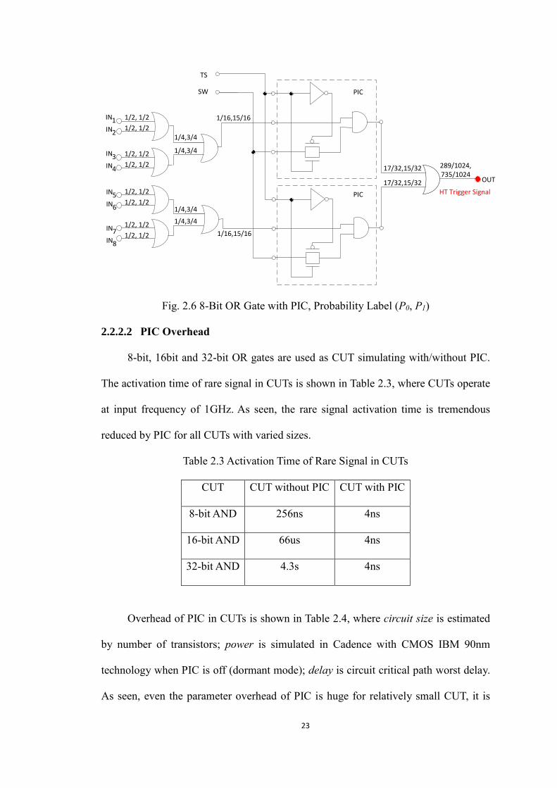
Fig. 2.6 8-Bit OR Gate with PIC, Probability Label (P0, P1)
2.2.2.2 PIC Overhead
8-bit, 16bit and 32-bit OR gates are used as CUT simulating with/without PIC.
The activation time of rare signal in CUTs is shown in Table 2.3, where CUTs operate
at input frequency of 1GHz. As seen, the rare signal activation time is tremendous
reduced by PIC for all CUTs with varied sizes.
Table 2.3 Activation Time of Rare Signal in CUTs
CUT CUT without PIC CUT with PIC
8-bit AND 256ns 4ns
16-bit AND 66us 4ns
32-bit AND 4.3s 4ns
Overhead of PIC in CUTs is shown in Table 2.4, where circuit size is estimated
by number of transistors; power is simulated in Cadence with CMOS IBM 90nm
technology when PIC is off (dormant mode); delay is circuit critical path worst delay.
As seen, even the parameter overhead of PIC is huge for relatively small CUT, it is

24
decreased linearly with the increase of corresponding CUT size. As discussed in section
2.2.1, the PIC overhead in a chip can be restricted by: 1) decrease the targeting transition
probability level; 2) apply less PIC in security-robust portion of circuit compared to
security-sensitive portion of circuit.
Table 2.4 Overhead of PIC for Rare Signal when 𝑃0 ≪ 𝑃1
CUT CUT without PIC CUT with PIC Overhead
Size
8-bit OR 42 62 47.6%
16-bit OR 90 106 17.8%
32-bit OR 186 202 8.6%
Power (µW)
8-bit OR 3.064 3.727 21.6%
16-bit OR 6.248 6.446 3.2%
32-bit OR 12.61 12.81 1.6%
Delay (ps)
8-bit OR 137 173 26.3%
16-bit OR 180 216 20%
32-bit OR 260 290 11.5%
2.3 PIC Insertion Algorithm
Circuit idle nodes remains in a signal status (either high or low) for most lifetime,
while leave another signal status as rare signal. The proposed PIC increases signal
transaction probability by using logic gates to generate rare signal in halftime. The
procedure of PIC insertion is shown in Fig. 2.7.
1. Calculate 𝑃0 and 𝑃1 for all nodes on chip based on input probabilities
(assume unknown input probabilities are equal, 𝑃0 = 𝑃1 ). Order nodes by
transition probability, which is equal to the product of 𝑃0 and 𝑃1.

25
2. Select transition probability threshold ( 𝑇𝑃𝑡 ). All nodes with transition
probability less than 𝑇𝑃𝑡 are classified in set A.
3. If set A is empty, all nodes with transition probability greater than threshold,
the process is done; otherwise, continue to next step.
4. Typically, rare situation accumulates by unbalanced signal probability one
level by one level from primary inputs to outputs, so nodes with less transition
probability may relatively after nodes with more transition probability.
Increasing transition probability of nodes closer to primary inputs will
somehow benefit transition probability of succeeding nodes. Therefore, PIC
is inserted to the first node (with maximum transition probability) in set A. Go
back to step 1.
Start
1. Order nodes by transition probability
2. Select threshold, nodes with transition probability
under the threshold are classified in set A
3. Set A is
empty?
4. Insert PIC on the first node in set A
End
no
yes
Fig. 2.7 PIC Insertion Flow
2.4 Experimental Result
A 64-bit binary comparator, shown in Fig. 2.8, is applied as CUT to evaluate the
effectiveness of the PIC insertion flow. Binary comparator is basic digital arithmetic
component that operates to compare two binary numbers. A 64-bit binary comparator

26
has two 64-bit binary input (𝐴63 -𝐴0 & 𝐵63 -𝐵0 ) and three binary outputs, which
indicate A>B, A<B, or A=B [35].
2-bit binary comparator
2-bit binary comparator
2-bit binary comparator
2-bit binary comparator
12-input comparator
A,B
3
3
3
6-input comparator
A=B
A>B
A<B
2-bit binary comparator
12-input comparator
12...
2-bit binary comparator
12-input comparator
12...
2-bit binary comparator
12-input comparator
12...
2-bit binary comparator
12-input comparator
48...
12-input comparator3
3
3
12-input comparator
12
3
Stage 1 Stage 2 Stage 3 Stage 4
A=B
A>B
A<Bn
A=B
A>B
A<B
A=B
A>B
A<B
63
A,B62
A,B61
A,B60
A,B59
A,B58
A,B57
A,B56
A,B55
A,B48
A,B47
A,B40
A,B39
A,B32
A,B31
A,B 0
1
n2
n3 n4
n5
n6
n7
n8
n9
n10
n11
n12
Fig. 2.8 64-Bit Binary Comparator
The signal probability of node is indicated as 𝑃𝑛𝑚 = (𝑃1, 𝑃0), in which n stands
for node, m is node number; 𝑃0 and 𝑃1 are probability of node with signal ‘0’ and ‘1’,
respectively. With assumption that primary inputs have 𝑃0 = 𝑃1, signal probability of
nodes in original 64-bit binary comparator are
𝑃𝑛1 = 𝑃𝑛2 = (3
8,5
8)
𝑃𝑛3 = (1
4,3
4)
𝑃𝑛4 = 𝑃𝑛5 = (1
2,1
2)
𝑃𝑛6 = (1
2248,2248−1
2248)
𝑃𝑛7 = 𝑃𝑛8 = (1
2,1
2)

27
𝑃𝑛9 = (232
2232 ,
2232−232
2232 )
𝑃𝑛10 = 𝑃𝑛11 = (1
2,1
2)
𝑃𝑛12 = (264
2264 ,
2264−264
2264 )
Signal transition probability (TP) is equal to the product of 𝑃0 and 𝑃1. Then TPs in
CUT are as following,
𝑇𝑃𝑛1 = 𝑇𝑃𝑛2 =3
8∗5
8≈ 0.23
𝑇𝑃𝑛3 =1
4∗3
4≈ 0.19
𝑇𝑃𝑛4 = 𝑇𝑃𝑛5 =1
2∗1
2≈ 0.25
𝑇𝑃𝑛6 =1
2248∗2248−1
2248≈ 0
𝑇𝑃𝑛7 = 𝑇𝑃𝑛8 =1
2∗1
2≈ 0.25
𝑇𝑃𝑛9 =232
2232 ∗
2232−232
2232 ≈ 0
𝑇𝑃𝑛10 = 𝑇𝑃𝑛11 =1
2∗1
2≈ 0.25
𝑇𝑃𝑛12 =264
2264 ∗
2264−264
2264 ≈ 0
The diminishing order of TP is 𝑇𝑃𝑛4 , 𝑇𝑃𝑛5 , 𝑇𝑃𝑛7 , 𝑇𝑃𝑛8 , 𝑇𝑃𝑛10 , 𝑇𝑃𝑛11 , 𝑇𝑃𝑛1 ,
𝑇𝑃𝑛2, 𝑇𝑃𝑛3, 𝑇𝑃𝑛6, 𝑇𝑃𝑛9, 𝑇𝑃𝑛12.
We set 0.1 as signal transition probability threshold (𝑇𝑃𝑡) in this example. Then
node 𝑛6 , 𝑛9 , and 𝑛12 are classified to set A (𝐴 = {𝑛6, 𝑛9, 𝑛12} ). According to
algorithm step 4, PIC is embedded in node 𝑛6 and other “A=B” signals in stage 2. This
circuit is denoted as 64-bit binary comparator with 1-level PIC.
Re-calculate signal probability and signal transition probability of nodes in 64-bit
binary comparator with 1-level PIC. The updated results are as:

28
𝑃𝑛1 = 𝑃𝑛2 = (3
8,5
8)
𝑃𝑛3 = (1
4,3
4)
𝑃𝑛4 = 𝑃𝑛5 = (1
2,1
2)
𝑃𝑛6 = (1
2,1
2)
𝑃𝑛7 = 𝑃𝑛8 = (1
2,1
2)
𝑃𝑛9 = (1
16,15
16)
𝑃𝑛10 = 𝑃𝑛11 = (1
2,1
2)
𝑃𝑛12 = (1
256,255
256)
𝑇𝑃𝑛1 = 𝑇𝑃𝑛2 =3
8∗5
8≈ 0.23
𝑇𝑃𝑛3 =1
4∗3
4≈ 0.19
𝑇𝑃𝑛4 = 𝑇𝑃𝑛5 =1
2∗1
2≈ 0.25
𝑇𝑃𝑛6 =1
2∗1
2≈ 0.25
𝑇𝑃𝑛7 = 𝑇𝑃𝑛8 =1
2∗1
2≈ 0.25
𝑇𝑃𝑛9 =1
16∗15
16≈ 0.06
𝑇𝑃𝑛10 = 𝑇𝑃𝑛11 =1
2∗1
2≈ 0.25
𝑇𝑃𝑛12 =1
256∗255
256≈ 0
Then, the updated set A consists of node 𝑛9 and 𝑛12. PIC is embedded in node 𝑛9
and other “A=B” signals in stage 3. This modified circuit is named 64-bit binary
comparator with 2-level PIC.
Repeat calculation for signal probability and signal transition probability of nodes
in 64-bit binary comparator with 2-level PIC. The updated results are as:

29
𝑃𝑛1 = 𝑃𝑛2 = (3
8,5
8)
𝑃𝑛3 = (1
4,3
4)
𝑃𝑛4 = 𝑃𝑛5 = (1
2,1
2)
𝑃𝑛6 = (1
2,1
2)
𝑃𝑛7 = 𝑃𝑛8 = (1
2,1
2)
𝑃𝑛9 = (17
32,15
32)
𝑃𝑛10 = 𝑃𝑛11 = (1
2,1
2)
𝑃𝑛12 = (289
1024,735
1024)
𝑇𝑃𝑛1 = 𝑇𝑃𝑛2 =3
8∗5
8≈ 0.23
𝑇𝑃𝑛3 =1
4∗3
4≈ 0.19
𝑇𝑃𝑛4 = 𝑇𝑃𝑛5 =1
2∗1
2≈ 0.25
𝑇𝑃𝑛6 =1
2∗1
2≈ 0.25
𝑇𝑃𝑛7 = 𝑇𝑃𝑛8 =1
2∗1
2≈ 0.25
𝑇𝑃𝑛9 =17
32∗15
32≈ 0.25
𝑇𝑃𝑛10 = 𝑇𝑃𝑛11 =1
2∗1
2≈ 0.25
𝑇𝑃𝑛12 =289
1024∗735
1024≈ 0.2
All updated TPs are greater than 𝑇𝑃𝑡 (0.1). The PIC insertion process is done.
The node with minimum signal transition probability in CUT without PIC and
CUT with 2-level PIC is 𝑛12 and 𝑛3, respectively. Assume that the rare signal in node
with minimum transition probability is used as HT trigger signal. Then, the average
number of primary input patterns that required to trigger HT is

30
𝑁 =1
𝑇𝑃𝑛12− 1 =
1
264
2264∗
2264−264
2264
− 1 ≈ 1.8 ∗ 1019
for CUT without PIC, and
𝑁 =1
𝑇𝑃𝑛3− 1 =
11
4∗3
4
− 1 ≈ 4
for CUT with 2-level PIC. Simulation results are listed in Table 2.5, where CUT is 64-
bit binary comparator; delay is circuit critical path worst delay; power is average power
consumption when PIC is off (in dormant mode); circuit size is estimated by number of
transistors; time stands for average time to active HT when input signal is at frequency
of 1GHz.
Table 2.5 Performance of CUT and PIC
CUT
CUT with 1-level PI CUT with 2-level PI
Parameter Overhead Parameter Overhead
Delay (ps) 712 840 18% 940 32%
Power (mW) 12.78 12.78 0% 12.8 0.2%
Size 1314 1434 1.5% 1414 7.6%
Time 570 years 256 ns 100% 4 ns 100%
As shown in Table 2.5, CUT with 1-level PI has the same improvement on HT
activation time compared to CUT with 2-level PI, however consumes almost half delay
overhead. Then 64-bit binary comparator with 1-level PI is chosen as the final modified
circuit. As seen, for the idlest node in original CUT that may take 570years to active
HT, the PIC insertion can even reduce the activation time to 256ns. It can be claimed
that the proposed PIC has ability to modify all nodes in CUT having an acceptable
signal transition probability.

31
2.5 Conclusion
A novel design (PIC) is introduced to increase transition probability of idle node
on chip that may be used as HT trigger signal. It may benefit HT detection by reducing
the HT activation time. 64-bit binary comparator is used to evaluate the effectiveness
of the PIC. Trigger time of rare signal in CUT is tremendously reduce with modest
circuit overhead.

32
3 Timing Analysis-based Hardware Trojan Detection
A timing analysis-based microelectronic circuit Hardware Trojan (HT) detection
methodology is proposed in this chapter. The detection circuit can be adopted in
combinational and sequential microelectronic circuits. The proposed technique is
implemented in IBM 90nm CMOS process and Xilinx ISE FPGA. Based on
experimental results, with one detection circuit embedded in testing-path, a HT with
size that is 2.81% of host-circuit size (15.63% of testing-path size) is detectable at
detection probability of 90% with a 10% probability of a false positives. Both detectable
HT size and detection probability can be improved by adding more detection circuits to
testing-path. The probability of false positives is controlled by the test clock period.
The discussion in this chapter is substantially drawn from [36][37], where we first
reported the development and evaluation of this technique.
3.1 Introduction
Recently, HT detection based on timing analysis has arisen as a popular technique.
Embedded HT will add extra capacitance, resulting in more charging and discharging
delays to Trojan affected paths. HT can be revealed by measuring the differential timing
characteristics of the attacked circuit.
Most publications based on timing analysis techniques focus on algorithms to
distinguish the timing difference caused by HT and methods to augment this difference.
Authors in [26] chose many clean (free of HTs) ICs and run a variety of input patterns
to record specific path delays establishing key delay fingerprints. Afterwards, circuit-
under-test (CUT) is tested under the same input patterns and verified by comparing
timing parameters with genuine fingerprint. Due to the complexity of millions of paths
in a complicated chip and instability of golden standards caused by inter and intra-die
variations, this method becomes infeasible for large circuit designs.

33
Instead of comparing with genuine fingerprint, authors in [38] compare the delay
of testing-paths with a set of symmetric paths, which are other paths that have the same
topology as the testing-paths. The delay of testing-paths and symmetric paths will be
the same unless an inserted HT breaks symmetry. Symmetry can naturally exist in ICs
or be artificially added. This method can avoid the difficulty and cost in finding a golden
model for all ICs with variable parameters. However, the detection accuracy suffers
from intra-die parameter variation, and the detection method is limited in that huge
area-overhead may emerge due to a bulk of artificial symmetries are required. Also,
massive effort is accumulated in finding existing symmetric paths and the specific test
vectors to measure desired path delays.
Authors in [39] increase the system clock frequency to create clock glitches until
resulting in faulty operation. Then the delay of IC critical paths for several bits are
estimated with the faulted outputs and the corresponding clock frequency. The
simulated path delays are compared to golden parameters to ascertain security reliability.
Statistical analysis method is introduced in [40] to facilitate the identification of HT. A
test-vector selection scheme and a novel timing measurement structure proposed in [41]
are effective in accurate path-delay measurement.
In [42], a HT detection method based on physical unclonable function (PUF) is
proposed, as shown in Fig. 3.1. It is used to detect HT in register-to-register paths. The
registers (FF1, FF2) in main circuit are triggered by the main system clock (clk1). HT
detection circuitry is within the dotted box, and the register in it (FF3) is triggered by
a shadow clock (clk2), which has the same frequency with main system clock (clk1)
and a controlled negative shift. The negative shift of shadow clock makes FF3 to be
triggered earlier than FF2, thereby output of combinational circuit arrives comparator
through FF3 ahead of it through FF2. Then the shadow clock negative shift is increased

34
until the register outputs are unequal. That clock shift time is claimed to be the
combinational circuit delay. The combinational circuit is suspicious of being HT-
attacked if the measured delay is substantially different from the pre-determined
designed timing. This technique is at-speed detection, which can be applied at both test-
time and run-time, but it requires extra circuit with large over-head to control skewed
clock (clk2). Moreover, it can only be used in sequential circuit register-to-register paths.
Combinational
CircuitFF1 FF2
FF3 comparator
clk2
clk1
inputoutput
result
clk1
clk2detection circuit
Fig. 3.1 Block Diagram of HT Detection Circuit Using PUF
A modified timing analysis-based HT detection technique is proposed in this
chapter, in which the clock skew control circuit is eliminated to simplify the detection
circuit. The experimental results show that the HT detection circuit overhead is
competitive compared to state-of-the-art with similar detection probability. The main
contributions of this technique are as follows:
• HT detection circuit area, timing, and power overhead on host-circuit are reduced.
The proposed detection circuit operates with main system clock, so the specific
clock skew control circuit (normally with thousands of gates) for HT detection is
eliminated.
• The proposed HT detection technique is not restricted to be applications with
register-to-register paths (e.g., [39][42]). This technique can be used on any
circuit path by isolating the path with extra registers.

35
• Location of HT can be estimated. The detection signals of each HT testing-path
are read out in series. The path of suspected HT can be determined by the location
of abnormal detection signal.
• Tunable detection probability to accommodate different security requirements of
circuit designs. HT detection probability can be increased by more detection
circuits pairing with one testing-path, meanwhile detection circuit overhead is
increased. The selection of testing-path paired with one detection circuit is
determined by chip designer based on vulnerability of the path, desired HT
resistance, and limitations on parameter overhead. For example, the security-
sensitive portion of circuit (e.g., memory) is required to be covered by more
detection circuits to achieve more accurate HT detection. Memory circuit is
security-sensitive, because the key data stored in memory could be a target for
attackers. While security-robust portion of circuit (e.g., critical path) can be
covered by less (or even zero) detection circuits to reduce workload and circuit
overhead. Critical path is security-robust, because any extra connection on critical
path will slow chip operating frequency, that can be easily revealed in post-fab
functional test.
3.2 Timing Analysis-based HT Detection
This section introduces the timing analysis-based HT detection algorithm,
functional block diagram and a sub-circuit design. To simplify the introduction of
detection algorithm, all cases in this section assume no manufacturing or environmental
variations, and experimental results are based on schematic simulation with tt (typical-
typical) corner. The effect of operating variations is considered in section 3.3.

36
3.2.1 Timing Analysis-based HT Detection Algorithm
In order to avoid detection, typically HTs are designed staying dormant until
activation. The proposed detection technique algorithm and implementation are with
premise that the HT remains dormant (sleeping mode) during detection process.
An HT circuit embedded in testing-path will add extra capacitance, resulting in
more charging and discharging delays to the testing-path [43][44]. The delay time (time
from applying an input pattern to signal arriving at output) will be increased for a HT-
attacked CUT compared to HT-free CUT due to the additional delay caused by HT
circuit. The input and output signals of testing-path with/without Trojan are shown in
Fig. 3.2, where 𝑡𝑐 is the designed delay of the testing-path. The proposed detection
method compares output signal at the calibrated CUT delay time (𝑡𝑐) and at double of
the calibrated CUT delay time (2𝑡𝑐) to facilitate HT detection. For ideal case, signal
arrives output at time 𝑡𝑐 in HT-free CUT, and the output signal remains fixed until
time 2𝑡𝑐 with assumption that input is unchanged, so the output at time 𝑡𝑐 and 2𝑡𝑐
are equal. In HT-attacked CUT, due to the increased delay caused by HT, signal arrives
at the output after a time greater than 𝑡𝑐, so the output at time 𝑡𝑐 and 2𝑡𝑐 are unequal.
Fig. 3.2 Signals in Trojan-Free (TF) and Trojan-Attacked (TA) Testing-Path
The flowchart of timing analysis-based HT detection algorithm consists of five
steps, as shown in Fig. 3.3. Based on circuit simulation, the delay time of Trojan-free
CUT testing-path is measured as D, which is used as golden reference (calibrated delay
time). Then input of testing-path is scanned in, and output at time D and 2D is captured
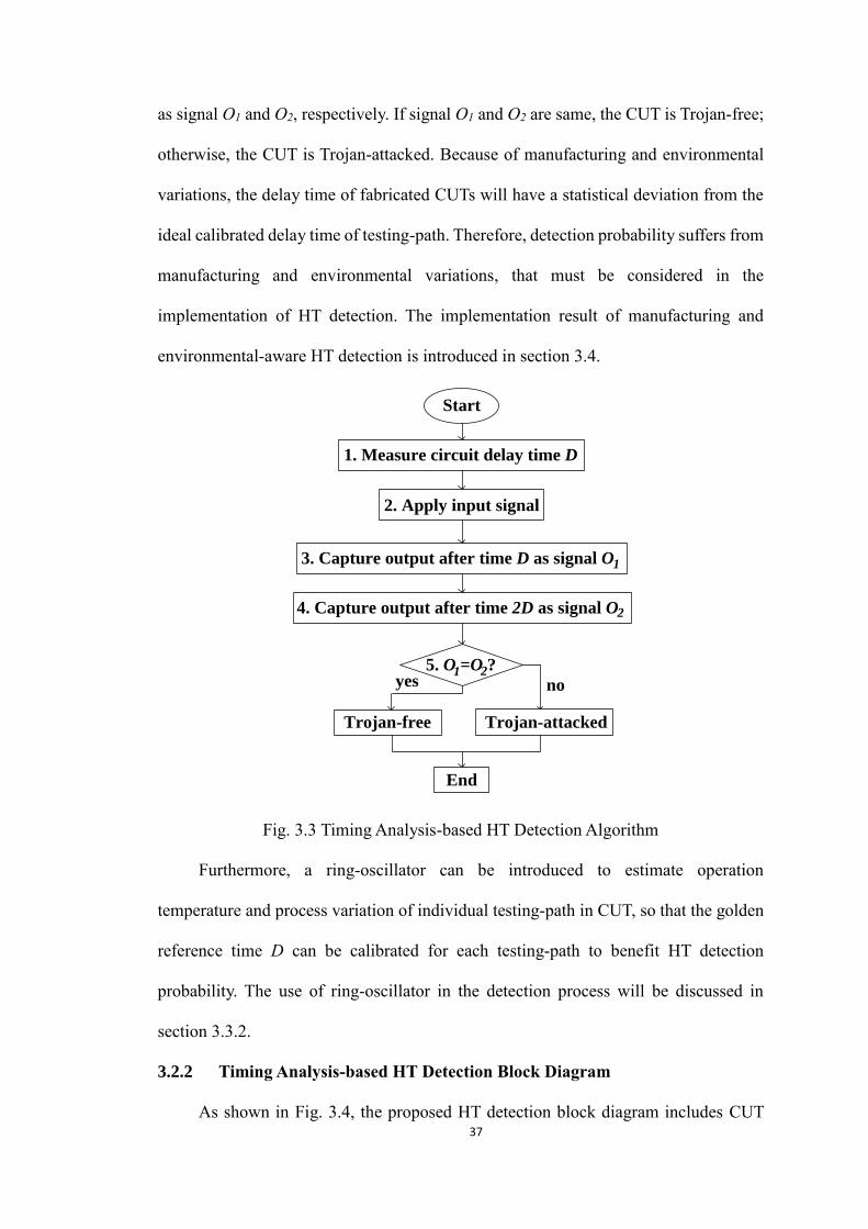
37
as signal O1 and O2, respectively. If signal O1 and O2 are same, the CUT is Trojan-free;
otherwise, the CUT is Trojan-attacked. Because of manufacturing and environmental
variations, the delay time of fabricated CUTs will have a statistical deviation from the
ideal calibrated delay time of testing-path. Therefore, detection probability suffers from
manufacturing and environmental variations, that must be considered in the
implementation of HT detection. The implementation result of manufacturing and
environmental-aware HT detection is introduced in section 3.4.
Start
1. Measure circuit delay time D
2. Apply input signal
3. Capture output after time D as signal O
4. Capture output after time 2D as signal O
5. O =O ?
Trojan-free Trojan-attacked
End
noyes
1
2
1 2
Fig. 3.3 Timing Analysis-based HT Detection Algorithm
Furthermore, a ring-oscillator can be introduced to estimate operation
temperature and process variation of individual testing-path in CUT, so that the golden
reference time D can be calibrated for each testing-path to benefit HT detection
probability. The use of ring-oscillator in the detection process will be discussed in
section 3.3.2.
3.2.2 Timing Analysis-based HT Detection Block Diagram
As shown in Fig. 3.4, the proposed HT detection block diagram includes CUT
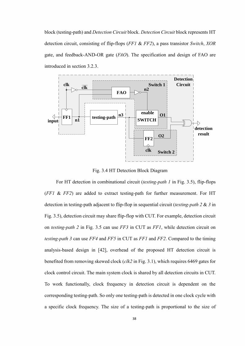
38
block (testing-path) and Detection Circuit block. Detection Circuit block represents HT
detection circuit, consisting of flip-flops (FF1 & FF2), a pass transistor Switch, XOR
gate, and feedback-AND-OR gate (FAO). The specification and design of FAO are
introduced in section 3.2.3.
FF1 testing-pathSWITCH
enable
FAO
FF2
clk
clk
clk
input
detection
result
n1
n2
n3 O1
O2
Detection
CircuitSwitch 1
Switch 2
Fig. 3.4 HT Detection Block Diagram
For HT detection in combinational circuit (testing-path 1 in Fig. 3.5), flip-flops
(FF1 & FF2) are added to extract testing-path for further measurement. For HT
detection in testing-path adjacent to flip-flop in sequential circuit (testing-path 2 & 3 in
Fig. 3.5), detection circuit may share flip-flop with CUT. For example, detection circuit
on testing-path 2 in Fig. 3.5 can use FF3 in CUT as FF1, while detection circuit on
testing-path 3 can use FF4 and FF5 in CUT as FF1 and FF2. Compared to the timing
analysis-based design in [42], overhead of the proposed HT detection circuit is
benefited from removing skewed clock (clk2 in Fig. 3.1), which requires 6469 gates for
clock control circuit. The main system clock is shared by all detection circuits in CUT.
To work functionally, clock frequency in detection circuit is dependent on the
corresponding testing-path. So only one testing-path is detected in one clock cycle with
a specific clock frequency. The size of a testing-path is proportional to the size of

39
detectable HT in the testing-path. More HT detection circuits applied on one testing-
path will increase detection probability, meanwhile resulting in more circuit over-head.
The selection and size of testing path are determined by chip designer and testing
engineer based on HT resistance to detection, the required HT detection probability,
and limitations on parameter overhead.
FF3input outputcombinational
logic
combinational
logic
combinational
logic
testing-path 1
CUT
testing-path 2 testing-path 3
FF4 FF5
Fig. 3.5 Testing-Path in CUT
The timing details of input and output waveforms for the proposed HT detection
applying on circuit in Fig. 3.4 is shown in Fig. 3.6. Signal propagation time of a testing-
path is measured as time D. The off-chip system clock period is set up as 2D. As seen
in Fig. 3.6, when detection starts, a rising edge input signal is scanned in; at next clock
positive edge (labelled as time t1), output of FF1 (node n1) captures the input rising.
The remaining circuit operations consider two cases: 1) Trojan-free, and 2) Trojan-
attacked.
1) Trojan-free circuit
In Trojan-free circuit, as shown in Fig. 3.6 (a), both n3 and O1 are pulled up
to ‘1’ at time D after input changes. FAO gate initializes when inputs are both ‘1’
or ‘0’, then functions as either an OR gate when output is ‘1’ or an AND gate when
output is ‘0’. The implementation of FAO is introduced in next section. Afterwards,
at the clock falling edge (labelled as time t2), two inputs of FAO (𝑐𝑙𝑘̅̅ ̅̅ & 𝑛1) are
both ‘1’, so output of FAO raises to ‘1’ and signal n2 falls to ‘0’ turn off SWITCH.
The detection circuit is designed so that signal propagation from n3 to O1 is faster
than that from clk to n2, then O1 rises before turning off SWITCH. Because FAO

40
gate functions as an OR gate when output is ‘1’, if one input of FAO (n1) remains
‘1’, the output of FAO gate will be ‘1’ regardless of another input (𝑐𝑙𝑘̅̅ ̅̅ ), eventually
SWITCH remains off. Signal n3 transfers to O2 through FF2 at next clock rising
edge (labelled as time t3). The detection result, which is equal to O1⨁O2, remains
low after time t3.
input
clk
n1
n2
clk
n3
(TF)
O
detection
(TF)
n3
(TA)
detection
(TA)t2
(a)
(b)t2't3
t1
D
1
(TF)
O2
(TF)
O1
(TF)
O2
(TF)
Fig. 3.6 Operation Waveform of HT Detection in Corner TT (typical-typical), (a)
Trojan-Free (TF), (b) Trojan-Attacked (TA)
41
2) Trojan-attacked circuit
In Trojan-attacked circuit, extra time is required to charge the HT capacitor
that is interfaced to testing-path. As shown in Fig. 3.6 (b), signal n3 is pulled up to
‘1’ at time 𝑡2′ which is later than t2. Because SWITCH is turned off at time t2,
signal O1 cannot capture n3 changes, and stays low. Signal O2 captures n3 through
FF2 at the succeeding clock rising edge (time t3). The detection result is pulled to
‘1’ at time t3.
After HT detection takes place, the detection result is read out by a scan-chain
that connects to detection result of all detection circuits in CUT. Then off-chip system
clock frequency is adjusted for next testing-path. This method can detect one testing-
path with one clock period.
The testing-path delay times will vary due to manufacturing and environmental
variations. The effect of these variations will be considered in section 3.3 with the
introduction of a probability of detecting an HT.
3.2.3 FAO Gate Implementation
FAO gate consists of two inputs (A & B), one output (�̅�), and it can be initiated
by applying inputs both ‘1’ or both ‘0’, then output �̅� is ’1’ or ‘0’, respectively. As
design specification, the function of FAO gate after initiation is represented by (3.1)
�̅� = {𝐴 ∙ 𝐵, 𝑤ℎ𝑒𝑛 �̅� = 0
𝐴 + 𝐵,𝑤ℎ𝑒𝑛 �̅� = 1 (3.1)
FAO transistor level design and paths operation are shown in Fig. 3.7 and Table
3.1, respectively. Output �̅� is uncertain before initiation. When inputs are “11”, pull-
down-path T7, T8 is on, output �̅� is initiated to ‘1’; when inputs are “00”, pull-up-path
T3, T2, T1/T4 is on, output �̅� is initiated to ‘0’. As seen in Table 3.1, FAO functions
as either an AND gate when ‘�̅�’ is ‘0’, or an OR gate when ‘�̅�’ is ‘1’. This design can
work as AND or OR gate that is dependent on circuit output signal, therefore the

42
proposed design is denoted as feedback-AND-OR gate.
T1
T2
T3 T6
T5
T4
T7
T8
T9
T10
T11
T12
B
A
A
Y
A
B A
Y
Fig. 3.7 Feedback-AND-OR (FAO) Gate
Table 3.1 Paths Operation in FAO Gate
Current Output Input Next Output
Path On
�̅� A B �̅�
0
0 0 0 T1/T4, T2/T5, T3/T6
0 1 0 T4, T5, T3/T6
1 0 0 T1, T2/T5, T6
1 1 1 T7, T8
1
0 0 0 T1/T4, T2, T3
0 1 1 T9, T10
1 0 1 T11, T12
1 1 1 T7, T8 / T9, T10 / T11, T12

43
3.2.4 Deployment of Timing Analysis-based HT Detection
There are several ways to categorize HT, such as categorizations based on
physical, activation, action, location characterization [4]. This section introduces HT
categorization based on location of HT, which can significantly vary the effect of HT
on host-circuit timing parameters.
HT
(b)
CUTinput output
HT
(a)
input outputCUT
HT
(c)
CUTinput output
Fig. 3.8 HT Location in CUT, (a) In-Path, (b) By-Path, (c) Off-Path
Based on location characteristics of Trojan in host-circuit, Trojan is partitioned
into three categories: in-path, by-path, and off-path, as shown in Fig. 3.8. When input
pattern is applied, the location of HT plays an important role on the ability to detect it.
The propagation signal in CUT will go through the extra paths caused by in-path HT,
which affects the measured transient time for some extend. The chip’s function can be
changed by an in-path HT through adding additional logic or bypassing the original
logic. A by-path HT affects the CUT’s original path by capacitive load introduced by
the HT, which affects the measured transient time for much less extend. A by-path HT
may be used to transit IC internal information to the attacker. Off-path HT is isolated
from the original circuit path, resulting in negligible timing alteration on original signal

44
propagation. An off-path HT may be used to tremendously change circuit temperature,
eventually modify the chip’s parametric properties, such as delay and power [5].
Although by-path and off-path HT has relatively tiny effect on path timing parameter,
HT’s control and action logic add extra Trojan circuit to the host-chip that will consume
extra power compared to original design. The detection of this type of Trojan is under
study based on combinational of power and timing-analysis in chapter 5. The proposed
method in this chapter is introduced for in-path and by-path HT detection.
3.3 Schematic Implementation
The HT detection circuit is implemented in Cadence Schematic with IBM 90nm
CMOS process. Monte Carlo analysis is used to account for operating variations.
The proposed HT detection method is implemented on 4, 8, 16-bit ripple-carry-
adders (RCAs) with in-path and by-path HTs, respectively. Signal n1 and n3 in Fig. 3.4
are carry-in (Cin) and carry-out (Cout) of RCA, respectively. Input vector of CUT is set
as Cout rises with Cin rising.
3.3.1 Operating Variation-Aware HT Detection
For ideal case, the circuit delay time will be increased (greater than 𝑡𝑐) for a HT-
attacked CUT compared to HT-free CUT due to the additional delay caused by HT
circuit, shown in Fig. 3.2, so the output at time 𝑡𝑐 and 2𝑡𝑐 are unequal. However, in
actual case, because of manufacturing process variation, circuit delay time varies in a
range, as shown in Fig. 3.9, in which the actual circuit delay varies in the range labelled
as from min to max. Increasing circuit calibrated delay time 𝑡𝑐 will cover more delay
cases in Trojan-free case that decreases HT detection false positive (FP), meanwhile
increased 𝑡𝑐 may miss more delays in Trojan-attacked case that decreases HT
detection probability. Also, as shown in Table 3.2, decreased 𝑡𝑐 will increase both

45
detection FP and detection probability. Note that false positive is the fault that asserts
Trojan-attacked for a Trojan-free circuit (false alarm).
output
(TF)tc
inputmin max
output
(TA)2t c
min max
Fig. 3.9 Ideal Signals in Trojan-Free (TF) and Trojan-Attacked (TA) Testing Path
Table 3.2 HT Detection Parameters with Variable Calibrated Delay Time
𝑡𝑐 False Positive Detection Probability
Increased Decreased Decreased
Decreased Increased Increased
To find the relationship of circuit fan-out and circuit timing alteration caused by
operating variation, an experimentation is set up as follows. Ten inverters connected in
serial, shown in Fig. 3.10 (a), is used as CUT with fan-out 1, while extra number of n-
1 inverters connected to each interval node, shown in Fig. 3.10 (b), is used as CUT with
fan-out n. The experimental results are listed in Table 3.3, in which ideal delay is based
on schematic simulation with tt (typical-typical) corner; actual delay is based on
schematic simulation with Monte Carlo analysis (100 iterations) to account for random
process variation and mismatch. As seen, the actual delay variation is decreased with
number of circuit fan-out increasing. Because it is rare that all fan-outs succeeding a
component pushing its process variation to limitation at the same direction. Therefore,
we claim that more fan-outs in a circuit design lead to low operating parameter
alteration associated with process variation, eventually benefit HT detection probability,

46
whereas attendant extra circuit delay.
input output
input output...
.
.
....
(a)
(b)
n
Fig. 3.10 CUT with fan-out 1 (a), and fan-out n (b)
Table 3.3 Delay of CUT with different fan-out
Fan-out Delay (ps)
Delay Variation Ideal Actual
1 133.87 105.84-174.01 29.98%
2 203.87 158.96-249.47 22.37%
3 275.14 221.92-329.87 19.89%
4 347.87 284.43-408.86 18.24%
5 421.02 355.48-489.70 16.31%
To prove that circuit with more fan-outs benefit HT detection probability, the
proposed timing analysis-based HT detection method is applied on a CUT (16-bit
ripple-carry-adder) with different number of fan-outs. Inverters are used connecting to
intermediate nodes to account for extra fan-outs. The experimental results are shown in
Table 3.4, in which HT detection is at detection probability of 90% with a 10%
probability of a false positives; the sum of widths of all NMOS and PMOS in circuit is
used to estimate circuit size. As seen, circuit with increased number of fan-outs possess
lower delay variation and ability to detect HT with smaller size that means detection
probability is increased.

47
Table 3.4 HT detection for CUT with different number of fan-outs
Fan-out
Host-Circuit Size
(μm)
Actual Delay Variation HT/Host-Circuit Size Ratio
1 170 28.73% 2.81%
2 173.84 27.62% 2.73%
3 177.68 27.15% 2.68%
4 181.52 26.87% 2.66%
5 185.36 26.51% 2.59%
3.3.2 Compensation of Manufacturing and Environmental Variations
Authors in [45] indicate that manufacturing and environmental variations can
cause up to 30% circuit performance difference. Also, the increased logic density and
operation frequency of modern ICs have exponentially magnified operational variations
due to temperature fluctuations. The increased temperature reduces transistor switching
speed, while increases transistor leakage current, that increases chip power
consumption and propagation delay.
To compensate these effects of variation on HT detection, a ring-oscillator, whose
frequency is temperature-dependent, is used to feed a counter, as shown in Fig. 3.11
[46]. The counter output can be read out to estimate ring-oscillator frequency. If the
ring-oscillator is layout-close to a testing-path, the environmental variations of testing-
path circuit can be estimated using ring-oscillator frequency. Then the calibrated delay
signature of the testing-path considering environmental variations may be used to
benefit HT detection probability.

48
Output Counter
Enable
Fig. 3.11 Ring-Oscillator Scheme
This technique is overhead-effective, and benefits detection probability in
individual testing-path in CUT. Due to the limitation of simulation tools, the ring-
oscillator is not implemented, but is introduced as a potential method to optimize the
detection probability.
3.3.3 In-Path HT Detection
HT occupying CUT path is defined as in-path HT, as shown in Fig. 3.8 (a). The
HT detection probability and detectable HT size in CUT are discussed in this section.
3.3.3.1 HT/Host-Circuit Ratio
To find how the size of testing-path will affect detection probability, a single
detection circuit is applied on three CUTs with different size (4, 8, 16-bit RCA). To
determine the calibrated circuit delay, flip-flops are added to input and output of the
RCA to find the maximum clock frequency of flip-flops while the RCA continues to
work functionally. Inverter buffers are randomly embedded in CUT testing-path to
account for HT. Both HT-free and HT-attacked CUTs are simulated by Monte Carlo
analysis (100 iterations) to account for random process variation and mismatch. The
detection results of HT-attacked CUTs are shown in Fig. 3.12.

49

50
Fig. 3.12 Detection of RCAs with In-Path HT, (a) 4-Bit, (b) 8-Bit, (c) 16-Bit RCA
False positive (FP) in Fig. 3.12 is the fault that asserts Trojan-attacked for a
Trojan-free circuit (false alarm). The probability of a FP in a Trojan-free circuit is
largely controlled by 𝑓𝑐𝑙𝑜𝑐𝑘. Increasing clock frequency constrains signal propagation
time from input to output of a test circuit. As clock frequency increases, measuring the
test circuit output at half the clock period and one clock period is more likely to produce
conflicting results thereby increasing the probability of a FP. Each test result is based
on averaging 100 Monte Carlo run and it turns out that probability of FP is essentially
constant for a given clock frequency. As seen in Fig. 3.12 (a) the probability of a FP is
0% if the clock frequency is equal to or less than 1.19GHz regardless of the HT size.
As clock frequency increases, the probability of FP increases, resulting in the plots of
the FP probability of 0, 10%, 20%, and 30%. On the other hand, a false negative (FN)
(100%-detection probability) is the fault that asserts Trojan-free for a Trojan-attacked
circuit. For a given clock frequency the probability of a FN is dependent on the relative
size of the HT compared to the test circuit size. As expected, the probability of a FN

51
decreases with HT size that is supported by the results in Fig. 3.12 where each result is
an average of 100 Monte Carlo runs. Each contour in Fig. 3.12 represents the
probability of a FN given a fixed FP. It is noted that 100%-FN% is the probability of
detecting the HT given a FP. For example, a 90% probability of detecting a HT given a
10% probability of a FP (asserting an HT when none is present) corresponds to FN and
FP being equal to 10%. The data in Table 3.5 has been extracted from the Fig. 3.12 plots
for equal values of FN and FP noting that 100%-FN% is the detection probability for a
given FP. The “Area overhead” in Table 3.5 is the size ratio of detection circuit over
CUT. The same detection circuit is applied to all three RCAs (input to output of 4, 8, or
16-bit RCA), but the total size of the RCA essentially doubles from 4 to 8 to 16-bits, so
the area overhead decreases with the number of bits. Longer signal propagation path
requires more transfer time, so the clock frequency for a given FP decreases and the HT
size for a given detection probability increases with the number of bits in RCA.
Table 3.5 In-Path HT Detection in RCAs
CUT
Area
Overhead
Detection Probability
(100%-FN)
FP
f𝑐𝑙𝑜𝑐𝑘
(GHz)
HT Size
(μm)
HT/Host-
Circuit Ratio
4-Bit RCA 14.04%
100% 0% 1.19 2.88 6.74%
90% 10% 1.32 1.44 3.37%
80% 20% 1.35 0.96 2.25%
70% 30% 1.39 0.48 1.13%
8-Bit RCA 7.03%
100% 0% 0.6 4.8 5.62%
90% 10% 0.65 2.88 3.37%
80% 20% 0.67 1.92 2.25%
70% 30% 0.69 1.44 1.69%
16-Bit 3.51% 100% 0% 0.31 8.16 5.89%

52
RCA 90% 10% 0.33 4.8 2.81%
80% 20% 0.34 4.32 2.53%
70% 30% 0.35 1.92 1.12%
To summarize, this detection technique facilitates essentially controlling the
probability of FP (false alarm) with the test circuit clock frequency while the probability
of detection is controlled by the relative size of HT to the test circuit size.
3.3.3.2 HT/Testing-Path Ratio
Path delay is the time from a path-input transition to a path-output transition. Path
delay is caused by capacitance in the signal propagation path which cannot be charged
or discharged instantaneously [47]. Signal propagates in circuit by switching the CMOS
networks on and off, charging and discharging each node capacitors through the entire
path. HT increases the circuit path delay by adding extra capacitance in testing-path.
The extra capacitance on testing-path caused by HT is denoted as HT on-path
capacitance. An important parameter affecting HT detection accuracy is the ratio of
detectable HT on-path capacitance to testing-path total capacitance.
Gate capacitance is used to estimate the size of both HT capacitance and CUT
capacitance. The capacitance at each node consists of driving load and self-load. Both
loads are proportional to the transistor width [48]. Then the sum of widths of all NMOS
and PMOS on testing-path is used to estimate circuit capacitance on testing-path for
both CUT and HT. The detectable HT size and testing-path size at detection probability
90% is listed in Table 3.6. The Testing-Path Size in Table 3.6 is the sum of widths of
transistors in CUT that directly interfaced to testing-path. The HT On-Path Size in Table
3.6 is the sum of widths of transistors in HT that directly connected to testing-path. As
seen, detectable HT size is proportional to testing-path size.
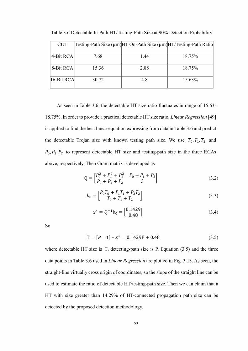
53
Table 3.6 Detectable In-Path HT/Testing-Path Size at 90% Detection Probability
CUT Testing-Path Size (μm) HT On-Path Size (μm) HT/Testing-Path Ratio
4-Bit RCA 7.68 1.44 18.75%
8-Bit RCA 15.36 2.88 18.75%
16-Bit RCA 30.72 4.8 15.63%
As seen in Table 3.6, the detectable HT size ratio fluctuates in range of 15.63-
18.75%. In order to provide a practical detectable HT size ratio, Linear Regression [49]
is applied to find the best linear equation expressing from data in Table 3.6 and predict
the detectable Trojan size with known testing path size. We use 𝑇0, 𝑇1, 𝑇2 and
𝑃0, 𝑃1, 𝑃2 to represent detectable HT size and testing-path size in the three RCAs
above, respectively. Then Gram matrix is developed as
Q = [𝑃02 + 𝑃1
2 + 𝑃22 𝑃0 + 𝑃1 + 𝑃2
𝑃0 + 𝑃1 + 𝑃2 3] (3.2)
𝑏0 = [𝑃0𝑇0 + 𝑃1𝑇1 + 𝑃2𝑇2
𝑇0 + 𝑇1 + 𝑇2] (3.3)
𝑥∗ = 𝑄−1𝑏0 = [0.14290.48
] (3.4)
So
T = [𝑃 1] ∗ 𝑥∗ = 0.1429P + 0.48 (3.5)
where detectable HT size is T, detecting-path size is P. Equation (3.5) and the three
data points in Table 3.6 used in Linear Regression are plotted in Fig. 3.13. As seen, the
straight-line virtually cross origin of coordinates, so the slope of the straight line can be
used to estimate the ratio of detectable HT/testing-path size. Then we can claim that a
HT with size greater than 14.29% of HT-connected propagation path size can be
detected by the proposed detection methodology.
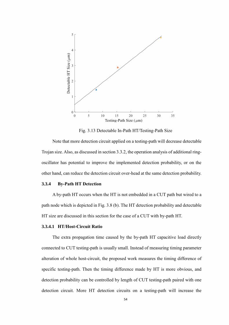
54
Fig. 3.13 Detectable In-Path HT/Testing-Path Size
Note that more detection circuit applied on a testing-path will decrease detectable
Trojan size. Also, as discussed in section 3.3.2, the operation analysis of additional ring-
oscillator has potential to improve the implemented detection probability, or on the
other hand, can reduce the detection circuit over-head at the same detection probability.
3.3.4 By-Path HT Detection
A by-path HT occurs when the HT is not embedded in a CUT path but wired to a
path node which is depicted in Fig. 3.8 (b). The HT detection probability and detectable
HT size are discussed in this section for the case of a CUT with by-path HT.
3.3.4.1 HT/Host-Circuit Ratio
The extra propagation time caused by the by-path HT capacitive load directly
connected to CUT testing-path is usually small. Instead of measuring timing parameter
alteration of whole host-circuit, the proposed work measures the timing difference of
specific testing-path. Then the timing difference made by HT is more obvious, and
detection probability can be controlled by length of CUT testing-path paired with one
detection circuit. More HT detection circuits on a testing-path will increase the

55
detection probability.
4, 8, 16-bit RCAs are used as CUT to implement by-path HT detection. Inverters
are randomly connected to nodes on the testing-path to account for by-path HT load to
CUT. Both Trojan-free and Trojan-attacked CUTs are simulated using Monte Carlo
analysis (100 iterations) to account for random process variation and mismatch. The
detection results of Trojan-attacked CUTs are shown in Fig. 3.14. As seen, with the
clock frequency corresponding to the same FP, HT detection probability is proportional
to Trojan size. The Trojan size is in term of the sum of widths of all NMOS and PMOS
transistors in HT that directly interfaced to the CUT. CUT with larger size requires
Trojan with larger size to achieve the same detection probability. The data in Table 3.7
has been extracted from the Fig. 3.14 plots for equal values of FN and FP noting that
100%-FN is the detection probability for a given FP.

56
Fig. 3.14 Detection of RCAs with By-Path HT, (a) 4-Bit, (b) 8-Bit, (c) 16-Bit RCA

57
Table 3.7 By-Path HT Detection in RCAs
CUT
Detection Probability
(100%-FN)
FP HT Size (μm) HT/Host-Circuit Ratio
4-Bit
RCA
100% 0% 3.6 8.42%
90% 10% 1.68 3.93%
80% 20% 1.2 2.81%
70% 30% 0.72 1.68%
8-Bit
RCA
100% 0% 6.24 7.30%
90% 10% 3.84 4.49%
80% 20% 2.88 3.37%
70% 30% 1.68 1.97%
16-Bit
RCA
100% 0% 9.84 7.68%
90% 10% 5.76 4.49%
80% 20% 4.56 3.56%
70% 30% 2.4 1.87%
3.3.4.2 HT/Testing-Path Ratio
As aforementioned, sum of transistor widths is used to estimate circuit size in this
chapter. The testing-path size and the minimum detectable HT size at detection
probability 90% are listed in Table 3.8. As seen, detectable HT size is proportional to
testing-path size. Note that, the implementation result has potential to be improved by
ring-oscillator. The HT/testing-path ratio in Table 3.8 is greater than that in the in-path
HT detection in Table 3.6. By-path HT is harder to detect compared to in-path HT.

58
Table 3.8 Detectable By-Path HT/Testing-Path Size at 90% Detection Probability
CUT Testing-Path Size (μm) HT On-Path Size (μm) HT/Testing-Path Ratio
4-Bit RCA 7.68 1.68 21.9%
8-Bit RCA 15.36 3.84 25%
16-Bit RCA 30.72 5.76 18.75%
Fig. 3.15 Detectable By-Path HT/Testing-Path Size
As seen in Table 3.8, the detectable HT size ratio fluctuates in range of 18.75-
25%. To predict a practical detectable HT size with known testing-path size, equation
(3.2)(3.3)(3.4) are used to achieve Linear Regression function of detectable by-path
HT/testing-path size ratio, as
T = [𝑃 1] ∗ 𝑥∗ = 0.1696P + 0.72 (3.6)
where detectable by-path HT size is T, detecting-path size is P. Equation (3.6) and the
three data points in Table 3.8 used in Linear Regression are plotted in Fig. 3.15. The
straight-line slope is used to estimate the ratio of detectable by-path HT/testing-path
59
size, thereby we can claim that a by-path HT with size greater than 16.96% of HT-
connected propagation path size can be detected by the proposed detection methodology.
3.3.5 Power-Overhead Analysis
The proposed detection technique will only be conducted off-line in conjunction
with functionality/reliability testing with emphasis on detection of HT inserted during
fabrication. The additional power consumed by the detection circuit in field would be
determined with the detection circuitry in passive (sleeping) mode. Then for detection
circuit power overhead measurement, the CUT is active while HT detection circuit is
dormant. To find power-overhead of the proposed detection circuit, a power
measurement experimentation is set up as follows. 4, 8, 16-bit RCAs are used as CUT,
respectively. Power consumption of CUT is measured when CUT operates at frequency
of 100MHz. Power consumption of CUT with detection circuit is measured when CUT
operates at same frequency of 100MHz while detection circuit is dormant. Detection
circuit in dormant mode will only consume static power. The static power consumption
of the same single detection circuit is fixed regardless of the size of corresponding CUT.
Therefore, power-overhead of detection circuit is inverse-proportional to the size of
CUT. The power measurement results are shown in Table 3.9. As seen, the power
consumption overhead of detection circuit is 1.2-3.7%, which is inverse-proportional
to the corresponding CUT size. Power consumption of detection circuits in 4, 8, 16-bit
RCAs are 0.8W, 0.91W, 0.9W, respectively. All the three RCAs are paired with the
same detection circuit. However, due to the different signals applied to detection circuit
by CUT testing path (signal n1 and n3 in Fig. 3.4), the detection circuit is in different
static power states thereby causing static power consumptions of detection circuit in
CUTs are slightly different.

60
Table 3.9 Power Consumption of CUT & HT Detection Circuit
CUT
Power Consumption (W)
Power Overhead
CUT CUT & Detection Circuit
4-Bit RCA 21.52 22.32 3.7%
8-Bit RCA 39.85 40.76 2.3%
16-Bit RCA 74.12 75.02 1.2%
3.4 Xilinx Implementation
An 8-bit digital finite impulse response filter (FIR) with order of 12 is
implemented in FPGA as CUT for HT detection experiment [50]. Digital FIR, shown
in Fig. 3.16, is a filter whose impulse response is of finite duration, because it settles to
zero in finite time. Each value of the output sequence is a weighted sum of the most
recent input values:
𝑦[𝑛] = ∑ 𝑏𝑖𝑥[𝑛 − 𝑖]𝑁𝑖=0 (3.7)
where 𝑥[𝑛] is input, 𝑦[𝑛] is output, N is filter order, 𝑏𝑖 is filter coefficient [51].
Fig. 3.16 Digital FIR Filter of Order n
The critical path of FIR is used as the HT testing-path. The XC6VLX240T FPGA
board, shown in Fig. 3.17, is deployed in this experimentation. FPGA internal signal
writing and reading are conducted using ChipScope, whose organization diagram is
shown in Fig. 3.18. A clock at 200MHz frequency is generated by Phase Locked Loop
(PLL) on board, then it is converted to required filter clock by Digital Clock Manager

61
(DCM). Integrated Controller (ICON) communicates with the host PC and sends
commands to other ChipScope modules via a control port. The Virtual Input/Output
(VIO) core is customized to drive a pulse train of successive values for CUT input
signal. CUT input, CUT output and HT-detection signals on FPGA are monitored and
send for display by Integrated Logic Analyzer (ILA) core.
Fig. 3.17 FPGA Board (XC6VLX240T)
Fig. 3.18 FPGA ChipScope Organization
The implementation results of FPGA, shown in Fig. 3.19, match the detection
Host PC with
Chipscope
ICON VIO
ILAFIR
filter
PLL DCM
control0
control1
trig0
sync_in sync_out
200MHz
clk
Top-level module
FPGA

62
algorithm: the detection signal remains low for Trojan-free CUT at second clock rising
edge, while it is pulled up to ‘1’ for Trojan-attacked CUT at second clock rising edge.
(a)
(b)
Fig. 3.19 FPGA Implementation Result of FIR Filter
Fabricated circuit operating variations include process, voltage, and temperature
(PVT) variation. To account for effect PVT variation on HT detection parameters, the
HT detection method is implemented on ten FPGA boards. The implementation results
are listed in Table 3.10, in which FPGA boards are ordered by CUT delay time. To
achieve 10% FP (false alarm) for Trojan-free circuit, CUT clock period is set up as
double of the ninth CUT delay (4.9ns), so that FPGA 1-9 can be correctly asserted to
be Trojan-free. The eighth detectable HT size is the minimum detectable Trojan size at
90% detection probability with 10% probability of FP. As seen in Table 3.10, an in-path
Trojan with size 0.7% of host-circuit and 3.2% of testing-path is detectable at detection
probability 90% with 10% false alarm. HT size ratio is less than schematic
implementation, because the limited FPGA chips have less process variation than

63
CMOS process modelling. The system clock frequency generated by DCM on FPGA
board is not continuous, so CUT delay and detectable HT size are not as accurate as
Cadence schematic implementation which can generate continuous clock frequency.
Table 3.10 Detectable HT Size in FPGA Boards
FPGA
Board
CUT
Delay (ns)
In-Path HT By-Path HT
HT/Host-
Circuit Ratio
HT/Testing-Path
Ratio
HT/Host-
Circuit Ratio
HT/Testing-Path
Ratio
1 4.7 0.5% 2.4% 0.9% 4.3%
2 4.7 0.5% 2.4% 0.9% 4.3%
3 4.7 0.5% 2.4% 1.1% 5.3%
4 4.8 0.7% 3.2% 1.1% 5.3%
5 4.8 0.7% 3.2% 1.1% 5.3%
6 4.8 0.7% 3.2% 1.1% 5.3%
7 4.8 0.7% 3.2% 1.1% 5.3%
8 4.9 0.7% 3.2% 1.2% 5.8%
9 4.9 0.7% 3.2% 1.3% 6.2%
10 5 0.9% 4% 1.4% 6.7%
3.5 Experimental Evaluation
This section clarifies three terms in this chapter: testing-path, host-circuit and
host-chip. They are important in understanding the HT detection parameters. Thereafter
benchmark circuits are used to evaluate the effectiveness of the proposed detection
method.

64
3.5.1 HT Detection Parameters
As mentioned before, the proposed HT detection circuit is applied on a selected
testing-path, which is a part of CUT. The host-circuit in the aforementioned detection
implementations is defined as the circuit associated with the testing-path. A low-power
carry-select-adder (CSA), shown in Fig. 3.20, is used to illustrate the HT detection
parameters for Trojan associate with testing-path, host-circuit and the whole host-chip
[52]. In this experiment, a HT circuit is randomly embedded in the testing-path, which
is from Cin to Cout in Fig. 3.20. With detection probability of 90% and 10% probability
of FP, the minimum detectable Trojan size is 0.24μm, which is 14.3% of the testing-
path size, 1.85% of the host-circuit size, and 0.09% of the host-chip (CSA) size. The
testing-path size is the size summation of transistors in CUT that directly connected to
the testing-path. The host-circuit size is the size of circuit in CUT that associate with
the testing-path, which is the circuit in dotted box in Fig. 3.20. The host-chip size in
this case is the size of CSA.
15:11 RCA
6-bit BEC
0
1
5 5A[15:11] B[15:11]
CY Mux 12:6
2 10
5
Sum[15:11]
10:7 RCA
5-bit BEC
0
1
4 4A[10:7]B[10:7]
CY Mux 10:5
2 8
4
Sum[10:7]
6:4 RCA
4-bit BEC
0
1
3 3A[6:4] B[6:4]
CY Mux 8:4
2 6
3
Sum[6:4]
c6
3:2 RCA
3-bit BEC
0
1
2 2A[3:2] B[3:2]
CY Mux 6:3
2 4
2
Sum[3:2]
c3
1:0 RCACin
2 2A[1:0] B[1:0]
2
Sum[1:0]
c1c10
o1o2o3o4
Cout
testing-path
Fig. 3.20 Low-Power Carry-Select-Adder
The detectable Trojan size ratio in section 3.3.3 and 3.3.4 is the ratio of Trojan
size over testing-path size or host-circuit size. Based on the implementations in section
3.3.3 and 3.3.4, the detectable Trojan size is one or two orders smaller than testing-path
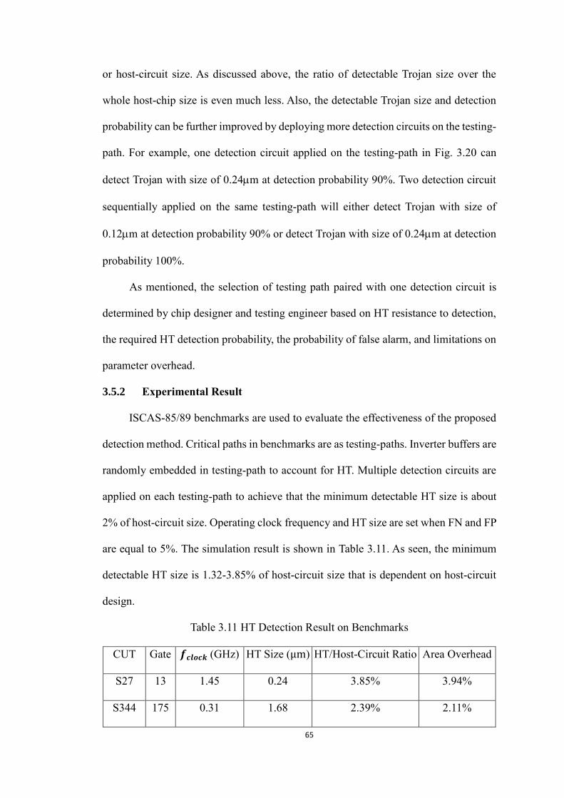
65
or host-circuit size. As discussed above, the ratio of detectable Trojan size over the
whole host-chip size is even much less. Also, the detectable Trojan size and detection
probability can be further improved by deploying more detection circuits on the testing-
path. For example, one detection circuit applied on the testing-path in Fig. 3.20 can
detect Trojan with size of 0.24m at detection probability 90%. Two detection circuit
sequentially applied on the same testing-path will either detect Trojan with size of
0.12m at detection probability 90% or detect Trojan with size of 0.24m at detection
probability 100%.
As mentioned, the selection of testing path paired with one detection circuit is
determined by chip designer and testing engineer based on HT resistance to detection,
the required HT detection probability, the probability of false alarm, and limitations on
parameter overhead.
3.5.2 Experimental Result
ISCAS-85/89 benchmarks are used to evaluate the effectiveness of the proposed
detection method. Critical paths in benchmarks are as testing-paths. Inverter buffers are
randomly embedded in testing-path to account for HT. Multiple detection circuits are
applied on each testing-path to achieve that the minimum detectable HT size is about
2% of host-circuit size. Operating clock frequency and HT size are set when FN and FP
are equal to 5%. The simulation result is shown in Table 3.11. As seen, the minimum
detectable HT size is 1.32-3.85% of host-circuit size that is dependent on host-circuit
design.
Table 3.11 HT Detection Result on Benchmarks
CUT Gate 𝒇𝒄𝒍𝒐𝒄𝒌 (GHz) HT Size (μm) HT/Host-Circuit Ratio Area Overhead
S27 13 1.45 0.24 3.85% 3.94%
S344 175 0.31 1.68 2.39% 2.11%

66
C499 202 0.46 2.16 2.66% 2.43%
C6288 2406 0.14 14.4 2.28% 1.9%
C5315 2406 0.08 20.4 1.32% 1.3%
Table 3.12 lists parameters of some recently published timing analysis-based HT
detection results. With similar detection probability, the proposed technique is
competitive in HT detection accuracy and sensitivity with relatively low overhead. Note
that the detectable HT size can be decreased by adding more detection circuits in one
testing-path, but its attendant more overhead.
Table 3.12 Comparison of HT Detection Methods
Reference Detection Probability False Positive Detectable HT Size Area Overhead
This Work 95% 5%
0.06-0.22%a
1.32-3.85%b
1.3-3.94%
Ngo [39] 95% 5% 1.7%a 0
Kelly [53] 100% 0 0.3%a 7.5%
Nejat [41] 97% 16% 6.1%b 20%
a minimum detectable HT size/host-chip size
b minimum detectable HT size/host-circuit size
3.6 Conclusion
A novel HT detection technique based on timing analysis is proposed. The
detection process of each testing-path takes one clock cycle. The detection method can
be adopted in both combinational and sequential circuit. Probability of detection FP
(false alarm) is effectively determined by the test clock frequency. For 90nm CMOS
ASIC benchmarks, the ratio of detectable HT size over host-circuit size ranged from
2.81% to 3.37% at 90% detection probability with 10% FP. For FPGA implementation

67
of HT detection, the ratio of detectable HT size to host-circuit size ranged from
approximated 0.5% to 0.9% at 90% detection probability. The detectable HT size and
detection probability can be further improved by applying more detection circuits on a
testing-path. Also, ring-oscillator can be introduced to estimate operation temperature
and process variation of testing-path to calibrate detection parameters, eventually
improve detection probability.

68
4 Self-Reference-based Hardware Trojan Detection
A self-reference-based power-analysis microelectronic circuit Hardware Trojan
(HT) detection methodology is proposed in this chapter. Simulation results show that
the proposed technique can detect HTs with areas that are 0.013% of the host-circuitry.
ISCAS benchmark circuits are used to evaluate efficiency of the developed method.
The discussion in this chapter is substantially drawn from [54][55], where we first
reported the development and evaluation of this technique.
4.1 Introduction
Recently, HT detection based on power analysis has arisen as an effective
technique. Embedded HT will add current paths and loads to the original circuit, that
result in extra power consumption on wires and gates in Trojan affected area. HT can
be revealed by measuring the differential power characteristics of the attacked circuit.
Most publications based on power analysis techniques focus on algorithms to
distinguish the power difference caused by HT and methods to augment this difference.
In [27], authors distinguish the HT-attacked chip by comparing the power traces of
circuit-under-test (CUT) with genuine circuit. Statistical methods are used to improve
the detection accuracy. This method is practical on HT with sufficient size to cause
detectable differences, however HT is normally designed with small size to maintain
the stealthy nature. It is difficult to directly distinguish the tiny effect of HT on a modern
complex chip. To augment the effect of HT, authors in [56] partition circuit into regions
using scan chains, then specific test vectors are generated to magnify the activity in the
target region. The power trace of the CUT is compared to golden parameters to ascertain
security reliability. Results show that the impact of HT on host-circuit is effectively
enlarged by this method. However, due to the instability of golden standards caused by
69
inter and intra-die variations and the maskable tiny power of HT caused by intrinsic
process and environmental variations of the host-chip, this method becomes practical
only for relatively large HT circuit designs. In [57], authors proposed a HT detection
method based on gate level characterization (GLC), in which a genuine-guaranteed chip
is not required. For each gate on chip, a manufacturing variability (MV) factor is
multiplied with ideal static power of the gate to account for MV effect on power profile.
To achieve more accurate results, thermal condition is considered for static power
calculation. Thereafter, a controlled input vector switching is used to adjust the thermal
conditioning of the entire chip to an expected level. A linear equation set is formulated
by the sum of calculated static power of each gate added a single HT variable is equal
to the measured static power of the whole chip. The HT variable is solved by a linear
program solver. The CUT is affirmed as Trojan-free if HT variable is close to 0;
otherwise, it is Trojan-attacked. To increase the detection accuracy in [57], CUT is
partitioned into segments using input vector selection in [58]. When the static power of
a segment is measured, a set of input vectors are applied to alter the static status of the
target segment while other segments are dormant.
A self-reference-based Trojan detection method is proposed in this chapter, in
which the effect of operating variations can be reduced by referencing neighbor
elements. The experimental results show that the HT detection accuracy is competitive
compared to state-of-the-art.
4.2 Preliminaries
This section introduces the basic design theory of the self-reference-based HT
detection.

70
4.2.1 Self-Reference-based HT Detection Theory
A sequential circuit is used as an example to explain this proposed technique. As
shown in Fig. 4.1, a CUT is partitioned into N segments excluding the system clock-
tree. The clock-tree is an essential net-work in modern chips to distribute clock to all
clocked elements at virtually the same time [59]. All partitioned segments in the CUT
must be controllable by primary inputs. Each segment uses a separate power rail, and
an on-chip clock-tree is powered by a specific rail in segment 0. To measure one
segment static power, the voltage supply is applied to this segment along with the clock-
tree rail, while leaving the other power rails float.
input output
Segment 0 Segment 1
Segment N
...clock-tree
...
clk
input
...
...
1
output
2
3
45
...
...
Fig. 4.1 Partitioned CUT
Considering an integrated circuit (IC) segment q with input pattern IN, the static
power measurement can be modeled as consisting of following components: (1) ideal
static power of component i in q, 𝑝𝑖(𝑞, 𝐼𝑁) which is dependent on operating segment
and input pattern. The ideal power is obtained by simulation based on tt (typical-typical)
corner analysis; (2) operating variations (process, voltage, temperature) effect on static
power of component i, 𝑛𝑣𝑖(𝑞, 𝐼𝑁, 𝑡) which is a random value, but it is influenced by

71
operating segment, input pattern, and operating time (t); (3) signal noise 𝑛𝑠(𝑞, 𝐼𝑁, 𝑡)
which depends on operating segment, input pattern, and operating time; (4) extra power
consumed by Trojan circuit 𝑝𝑇(𝑞, 𝐼𝑁, 𝑡) if segment is attacked by Trojan circuit.
Therefore, static power measurement of Trojan-free segment q with k components can
be modeled by (4.1)
𝑃𝑚𝑒𝑠(𝑞, 𝐼𝑁, 𝑡) = ∑ (𝑝𝑖(𝑞, 𝐼𝑁) + 𝑛𝑣𝑖(𝑞, 𝐼𝑁, 𝑡))𝑘𝑖=1 + 𝑛𝑠(𝑞, 𝐼𝑁, 𝑡) (4.1)
and static power of the Trojan-attacked q is
𝑃𝑚𝑒𝑠(𝑞, 𝐼𝑁, 𝑡) = ∑ (𝑝𝑖(𝑞, 𝐼𝑁) + 𝑛𝑣𝑖(𝑞, 𝐼𝑁, 𝑡))𝑘𝑖=1 + 𝑛𝑠(𝑞, 𝐼𝑁, 𝑡) + 𝑝𝑇(𝑞, 𝐼𝑁, 𝑡) (4.2)
The random signal noise 𝑛𝑠(𝑞, 𝐼𝑁, 𝑡) can be largely eliminated by averaging
over a number of power measurements for the same IC. So signal noise is ignored in
(4.1) and (4.2). Fabricated circuit operating variations include process, voltage, and
temperature (PVT) variation. The same component in q will have the same process and
voltage variation for different input pattern IN. Different IN will result in different
power consumption and eventually vary operating temperature. A specific operating
variable scaling factors (λ) is introduced to account for the average PVT variation on a
circuit component compared to the ideal static power consumption. The static power of
genuine q and Trojan-attacked q are modeled as (4.3) and (4.4), respectively.
𝑃𝑚𝑒𝑠(𝑞, 𝐼𝑁, 𝑡) = ∑ 𝜆𝑖𝑝𝑖(𝑞, 𝐼𝑁)𝑘𝑖=1 (4.3)
𝑃𝑚𝑒𝑠(𝑞, 𝐼𝑁, 𝑡) = ∑ 𝜆𝑖𝑝𝑖(𝑞, 𝐼𝑁) +𝑘𝑖=1 𝑝𝑇(𝑞, 𝐼𝑁, 𝑡) (4.4)
Equation (4.4) accounts for the extra Trojan power consumption, but is not used
in the self-reference-based detection methodology. Equation (4.3) is used as power
measurement model in the rest of this chapter. Inserting Trojan will increase power
consumption (𝑃𝑚𝑒𝑠 ) in (4.3), meanwhile 𝑝𝑖 is fixed from tt corner simulation.
Therefore, the λ value in Trojan-attached circuit will be increased compared to Trojan-
free circuit.

72
The proposed HT detection methodology is based on solving for each component
λ and clock-tree λ with the pre-determined (simulated) ideal static power (𝑝𝑖) of each
component and measured power (𝑃𝑚𝑒𝑠) of each segment with different input patterns.
HT-attacked assertion in each segment is based on the λ𝑐𝑙𝑘 for that segment falling
outside of prescribed limits. The prescribed limit of λ𝑐𝑙𝑘 for a specific segment is
dependent on reference of the values of λ𝑐𝑙𝑘 in other segments of the chip. So, this
technique is denoted as self-reference-based HT detection.
Basically, this detection method uses a global component to estimate the
parametric stability of each partitioned segment. The clock-tree is used as a global
component in this chapter, since most practical chip designs including both
combinational and sequential circuits are with a clock-tree to meet modern circuit
requirements, high operating frequency and high resolution. For detection on
combinational circuit only chips without clock-tree, this method needs to use other
global circuits as reference component, such as a power-gating control circuit.
The main contributions of this technique are as follows:
• HT detection method can be applied with zero-overhead.
• Genuine chip is not needed.
• Location of HT can be estimated.
• Partitioned CUT increases detection accuracy.
• Detection accuracy is adjustable by size of partitioned segments.
• Computational complexity is optimizable based on required detection accuracy.
There is a potential I/O issue with this technique because each partitioned
segment requires a separate pair of power rail (𝑉𝐷𝐷 , 𝐺𝑁𝐷), which occupies two I/O pins.
So, the number of required power pins may increase with the number of partitioned
segments. However, to have a stable power source, chip designers usually provide a

73
number of I/O pads for power rails. For example, in MIPS processor, 11 out of 40 I/O
pads are used for power rails [60][61]. Then the existing power pads can be employed
to separate power segments. Furthermore, a multiplexer can be exploited to control
more power rails for segments with limited I/O pins. To achieve the maximum detection
accuracy with zero overhead, all existing power pads should be exploited to separate
power segments, that means the number of partitioned segments (N) should follow 2 ∗
𝑁 = 𝑛𝑝(or 2 ∗ 𝑁 = 𝑛𝑝 − 1 if 𝑛𝑝 is odd), where 𝑛𝑝 is the number of power pads.
Note that chip designer can further increase detection accuracy by partition circuit into
more segments, but its attendant overhead by extra control circuit splitting the existing
power rails.
Compared to the conventional practical HT detection methodologies using
variation factors and portioned CUT, the uniqueness of the proposed method is stated
as follows:
• The power measurement of each partitioned segment is more accurate,
that will benefit the HT detection probability. In the proposed method, when the
power of a circuit segment is measured, other circuit segments are physically
isolated from power rails. The conventional methods either emphasize the power
of target segment by magnifying the activity of target region or achieve the power
of partitioned segment by mathematic analysis [56][58].
• The operating variable scaling factors (λ) of a global component is used to
estimate the parametric stability of each partitioned segment. The segment is
asserted as Trojan-attached if λ of global component exceeds prescribed limit in it.
It is more efficient compared to conventional HT detection method using variation
factors, which requires massive math analysis for the scaling factor of each gate on
chip.

74
• HT detection overhead and workload can be adjusted by chip designer
based on vulnerability of path, the desired HT resistance, and limitations on
parameter overhead. For example, the security-sensitive portion of circuit (e.g.,
memory) is required to be covered by segment with smaller size (e.g., number of
gates) and more power profiles need to be measured to achieve more accurate HT
detection. The reason why more power profiles benefit detection accuracy is
explained by Fig. 4.6 in section 4.3. Memory circuit is security-sensitive, because
the key data stored in memory could be a target for attackers. While security-robust
portion of circuit (e.g., critical path) can be covered by larger segment and less
power measurements can be conducted to reduce workload and circuit overhead.
Critical path is security-robust, because any extra connection on critical path will
slow chip operating frequency, which can be easily revealed in post-fab functional
test. Moreover, if detection accuracy is not critical for a segment, the operating
variation scaling factor (λ) can be used for a group of multiple gates instead of
single gate to tremendously reduce the computational complexity of the detection
methodology, which is introduced in section 4.3.3.
4.2.2 Operating Variation
Because of variations of physical parameters and fabrication process parameters,
transistors may have different threshold voltage (𝑉𝑡) and channel length (𝐿). In addition,
interconnect lines may have different width, thickness, and contact resistance. All these
can affect circuit design timing and power parameters. This situation is denoted as
process variation that can cause up to 30% circuit performance variation in 90nm
technology [62].
Power supply voltage may vary up to 10% due to capacity of voltage regulator,
IR drops along supply rail, and noise. This will further alter the power consumption and

75
delay of a designed circuit [46].
Also, the increased logic density and operating frequency of modern ICs have
exponentially magnified operational variations due to temperature fluctuations.
Increased temperature reduces transistor switching speed meanwhile increases
transistor leakage current, that increases chip power consumption and propagation delay.
Normally, HTs are designed to remain dormant until activation to avoid detection.
However, the embedded HT causes leakage current even in sleeping mode that
contributes to static power consumption of host-circuit. Therefore, detection of an HT
in the sleeping mode is dependent on static power consumption. Static power is
negligible compared to dynamic power, so circuit activity causing dynamic power will
dramatically reduce the power contribution of dormant HT on host-circuit. Also, PVT
variations affect static power to a lesser extent than dynamic power. Circuit static power
follows a Gaussian distribution as a function of PVT variations with the magnitude of
the 3 standard deviation about 19% of the mean value [63]. Retaining parts within a
3 distribution will result in 0.26% of parts being rejected.
To check whether the input patterns and PVT variations affect circuit static power
or not, a power measurement experimentation is set up as follows. A 1-bit full adder
(FA) is simulated with all eight input patterns using Monte Carlo analysis to account
for PVT variations. Three input patterns are randomly picked from Monte Carlo
analysis (50 iterations for each input pattern). For each of the 50 Monte Carlo
simulations, a ratio is calculated which is equal to the Monte Carlo simulated power
consumption (measured power) over the designed power consumption (ideal simulated
result with typical/typical model parameters). This ratio is calculated for static power
consumption of an AND gate (G1) in the FA and is plotted in Fig. 4.2. Each axis
represents measured over designed static power of G1 for each input pattern. Each

76
bubble is located by measured power over ideal power of G1 in the same Monte Carlo
iteration with each of the three possible input pattern simulations. All dots on the red
solid line in Fig. 4.2 have equal x, y, z values (same ratio of measured to simulated
power for all three input patterns). As seen in Fig. 4.2, all bubbles distribute along the
red line, but vary from 0.8 to 1.4 as PVT variation, which indicates the power deviation
changes greatly with Monte Carlo PVT variations, but remains relatively close to the
same value for all three input patterns for the same Monte Carlo iteration (same PVT
parameters).
Fig. 4.2 Static Power Deviation of Gate G1
As mentioned in section 4.2.1, to account for the PVT effect on static power
consumption of any designed circuits, a scaling factor 𝜆𝑖 is introduced to estimate the
real static power of gate i based on ideal simulated power as 𝜆𝑖𝑝𝑖𝑗, where 𝑝𝑖𝑗 is the
ideal static power of gate i with input vector j. Similarly, a scaling factor 𝜆𝑐𝑙𝑘 is used

77
to estimate the real static power of a clock-tree as 𝜆𝑐𝑙𝑘𝑝𝑐𝑙𝑘 where 𝑝𝑐𝑙𝑘 is the ideal
static power of the clock-tree.
4.3 Self-Reference-based HT Detection
This section introduces the proposed HT detection algorithm and mechanism.
Benchmark circuits are used as examples to explain the detection methodology and
optimization of computational complexity.
4.3.1 Self-Reference-based HT Detection Algorithm
The flowchart of self-reference-based HT detection algorithm consists of six steps
as shown in Fig. 4.3.
Start
1. Partition Circuits into Segments
2. Table Static Power of Each Gate
3. Measure Static Power in Testing Segment
4. Calculate Scaling Factors of Clock-
tree (λ ) based on Testing Segment q.
λ
Trojan-freeTrojan-attacked
End
no yes
5. Iterate for Remaining Segments.
clkq
clkq qΛ ∈6.
Fig. 4.3 Overall Flow of Self-Reference-based HT Detection

78
1) Partition CUT into 𝑁 segments, and ensure clock-tree is in a separate single
segment. N circuit segments use N separated power rails. HT detection accuracy is
proportional to the ratio of HT size to the segment size where HT is located. In other
words, detection accuracy rises with number of partitioned segments (𝑁) in CUT while
all the partitioned segments are roughly equal in size. (Note size is estimated by total
CMOS transistor width.)
2) Table the ideal (simulation data in tt corner) designed static power consumption
of each gate with specified input patterns for each segment.
3) Power on one segment together with clock-tree, while power rails in other
segments float. Measure static power consumption of CUT (𝑃𝑚𝑒𝑠) with different input
patterns.
4) To determine the mean effect of PVT variations on designed circuits, the ideal
static power consumption of clock-tree (𝑝𝑐𝑙𝑘 ) and gates (𝑝𝑖 ) is multiplied by an
operating variation scaling factor (𝜆). A set of m equations is formulated as shown in
(4.5) with assumption that the testing segment consists of k gates with m static states.
Each static state is a state with specific static power consumption.
𝑃𝑐𝑎𝑙𝑗 = ∑ 𝜆𝑖𝑝𝑖𝑗𝑘𝑖=1 + 𝜆𝑐𝑙𝑘𝑝𝑐𝑙𝑘, 𝑗 = 1…𝑚 (4.5)
where 𝑃𝑐𝑎𝑙𝑗 is the static power consumption of CUT with static state 𝑗, 𝜆𝑖 is scaling
factor of gate 𝑖, 𝑝𝑖𝑗 is ideal static power of gate 𝑖 with static state 𝑗. The unknown
variables in (4.5) are 𝜆𝑖 and 𝜆𝑐𝑙𝑘.
A combinational circuit with 𝐾𝑖𝑛 primary inputs has 2𝐾𝑖𝑛 possible number of
static states. In a sequential circuit, registers are used to divide sections of
combinational logic, as shown in Fig. 4.4. For the sequential circuit in Fig. 4.4 with
𝐾𝑖𝑛 inputs, there are 2𝐾𝑖𝑛 static states for each combinational logic. Primary input
signals propagate through one section of combinational logic in each clock cycle. Each
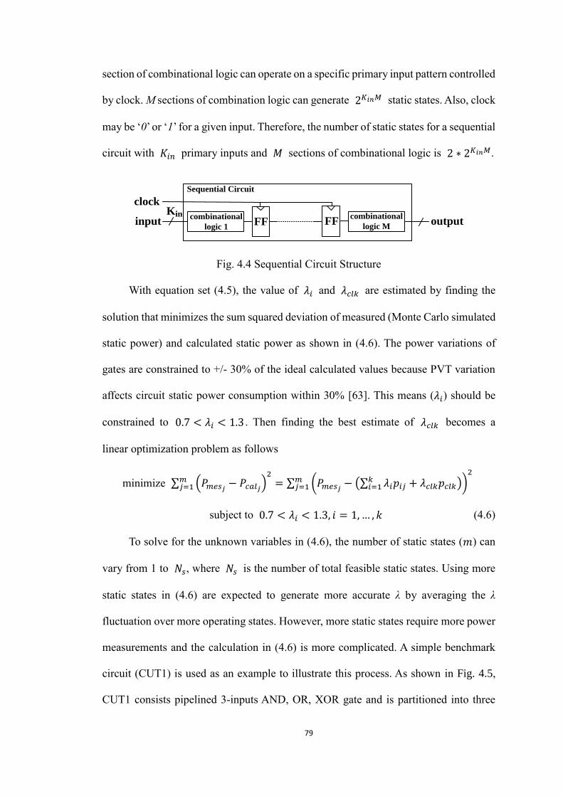
79
section of combinational logic can operate on a specific primary input pattern controlled
by clock. M sections of combination logic can generate 2𝐾𝑖𝑛𝑀 static states. Also, clock
may be ‘0’ or ‘1’ for a given input. Therefore, the number of static states for a sequential
circuit with 𝐾𝑖𝑛 primary inputs and 𝑀 sections of combinational logic is 2 ∗ 2𝐾𝑖𝑛𝑀.
FF FFcombinational
logic 1input output
Kin
clock
combinational
logic M
Sequential Circuit
Fig. 4.4 Sequential Circuit Structure
With equation set (4.5), the value of 𝜆𝑖 and 𝜆𝑐𝑙𝑘 are estimated by finding the
solution that minimizes the sum squared deviation of measured (Monte Carlo simulated
static power) and calculated static power as shown in (4.6). The power variations of
gates are constrained to +/- 30% of the ideal calculated values because PVT variation
affects circuit static power consumption within 30% [63]. This means (𝜆𝑖) should be
constrained to 0.7 < 𝜆𝑖 < 1.3 . Then finding the best estimate of 𝜆𝑐𝑙𝑘 becomes a
linear optimization problem as follows
minimize ∑ (𝑃𝑚𝑒𝑠𝑗 − 𝑃𝑐𝑎𝑙𝑗)2
𝑚𝑗=1 = ∑ (𝑃𝑚𝑒𝑠𝑗 − (∑ 𝜆𝑖𝑝𝑖𝑗 + 𝜆𝑐𝑙𝑘𝑝𝑐𝑙𝑘
𝑘𝑖=1 ))
2𝑚𝑗=1
subject to 0.7 < 𝜆𝑖 < 1.3, 𝑖 = 1,… , 𝑘 (4.6)
To solve for the unknown variables in (4.6), the number of static states (𝑚) can
vary from 1 to 𝑁𝑠, where 𝑁𝑠 is the number of total feasible static states. Using more
static states in (4.6) are expected to generate more accurate λ by averaging the λ
fluctuation over more operating states. However, more static states require more power
measurements and the calculation in (4.6) is more complicated. A simple benchmark
circuit (CUT1) is used as an example to illustrate this process. As shown in Fig. 4.5,
CUT1 consists pipelined 3-inputs AND, OR, XOR gate and is partitioned into three

80
segments plus one clock-tree segment. Each partitioned segment consists of two
combinational gates and one sequential gate (a D flip-flop). To account for process
variation, the benchmark circuit is simulated with Monte Carlo analysis including
process variation and mismatch. The simulated Monte Carlo results are referred to as
the measured values. Scaling factor of the clock-tree (𝜆𝑐𝑙𝑘) is calculated with number
of static states varying from 4 to 10. For each number of static states, there are 𝐶𝑁𝑠𝑚
static state combinations that can be chosen, where 𝑁𝑠 is the number of total feasible
static states, and 𝑚 is number of selected static states. For example, all segments in
CUT1 have 32 static states. For each segment, a set of 4, 5, …, 10 static states are
selected from the possible 32 states and 𝜆𝑐𝑙𝑘 deviation from ideal value of 1 resulting
from solving (4.6) for each segment is plotted in Fig. 4.6.
FF
A1B1C1
Y1
FFA2
B2
C2 Y2
FF
A3 B3 C3
Y3
Segment 1
Segment 2 Segment 3
Segment 0
clock-treeclk 12 3
1 12 23 3
Fig. 4.5 Partitioned CUT1

81
Fig. 4.6 𝜆clk Deviation in CUT1
In Fig. 4.6, “𝜆𝑐𝑙𝑘 deviation” represents deviation of calculated 𝜆𝑐𝑙𝑘 from ideal
value of 1; 𝜆𝑐𝑙𝑘𝑞 is the 𝜆𝑐𝑙𝑘 based on calculation in segment q. As seen, a larger
number of static states results in a solution that converges to a more accurate estimate
of 𝜆𝑐𝑙𝑘.
5) Iterate step 3, 4 for the remaining segments.
6) Define that deviation of clock-tree scaling factor in segment q is
𝛬𝑞 =𝜆𝑐𝑙𝑘𝑞−min (𝜆𝑐𝑙𝑘1,…,𝜆𝑐𝑙𝑘𝑁)
min (𝜆𝑐𝑙𝑘1,…,𝜆𝑐𝑙𝑘𝑁) (4.7)
Constraints must be placed on the threshold of values for 𝛬𝑞 for declaring a Trojan-
free or Trojan-attached segment. Seven Trojan-free benchmark circuits are designed in
IBM 90nm CMOS technology and simulated with Monte Carlo analysis (100 samples).
The simulation results are plotted in Fig. 4.8, where false negative is the fault that assert
Trojan-attacked for a Trojan-free circuit; CUT1, CUT2 are customized benchmarks,
shown in Fig. 4.5 and Fig. 4.9, respectively; s27 and s344 are ISCAS-89 benchmarks;
c499, c6288 and c5315 are ISCAS-85 benchmarks, shown in Fig. 4.7.

82
ISCAS-89 s344 is a 4-bit multiplier which consists of 16 multiplexers, 12 D flip-
flops, 3 T flip-flops, one 4-bit full adder, and one 4-bit AND gate. ISCAS-85 c499 is a
single-error-correcting circuit [64]. The 41 inputs are combined in module M1 to form
an 8-bit internal bus S, which then combines with 32 primary inputs in module M2
consisting correcting logic. Benchmark c6288 is a 16*16 multiplier formed by a 15*16
matrix with 240 full and half adders. Benchmark c5315 is a 9-bit arithmetic logic unit
(ALU) that performs arithmetic and logic operations simultaneously on two 9-bit input
signals.
R
IC
ID
M1
S S
ID
OD
M2
Syndrome
8
1
8
32
R
IC
ID32
OD
(c)
Q
QSET
CLR
D
Q
QSET
CLR
D
Q
QSET
CLR
D
A
B
C
D
clk
Y
(a)
MFF
D AddM
FF
D
MFF
DM
Cntr C
4A
4
P04
4
4
4 4P4-7
Shift Start
4B
444
ReadyShift
P0-3
Start Ready
CNTVCO2
CNTVCON2
Ready
Load_A
Shift
(b)

83
(d)
P0P1
P2
P3
P4
P5
P6
P7
P8
P9
P10
P11
P12
P13
P14
P15
P16P17P18P19P20P21P22P23P24P25P26P27P28P29P30P31
Half Adder
Full Adder
M1
X0(8:0)
X1(8:0)
X
S
M2
Y0(8:0)
Y1(8:0)
Y
S
X(8:0)
X0(8:0)A(8:0)
CinPX
WpX(1:0)
CP(3:0) MuxSel(10:9)
CalcParity
PoXMuxesPar
ParX
Y(8:0)
Y0(8:0)B(8:0)
CinPY
WpY(1:0)
CP(3:0) MuxSel(10:9)
CalcParity
PoY
ParY
QP1
QP2
QP3
QP4
OP1
OP2
OP3
OP4
MuxSel(8:0)
X(8:0)
X0(8:0)A(8:0)
CinFX
WFX(8:0)
CF(7:0) MuxSel(10:9)
Add-Logic
CoXMuxesF
FX(8:0)
Y(8:0)
Y0(8:0)B(8:0)
CinFY
WpY(8:0)
CF(7:0) MuxSel(10:9)
CalcParity
CoY
FY(8:0)
QF1(8:0) OF1(8:0)
MuxSel(8:0)
SumX LogicX
QF2(8:0)
QF3(8:0)
QF4(8:0)
OF2(8:0)
OF3(8:0)
OF4(8:0)
SumY LogicY
NFX(8:0)
NFY(8:0)
(e)
Fig. 4.7 ISCAS-89 Benchmarks (a) S27, (b) S344, and ISCAS-85 Benchmarks (c)
c499, (d) c6288, (e) c5315
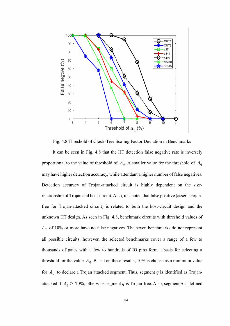
84
Fig. 4.8 Threshold of Clock-Tree Scaling Factor Deviation in Benchmarks
It can be seen in Fig. 4.8 that the HT detection false negative rate is inversely
proportional to the value of threshold of 𝛬𝑞. A smaller value for the threshold of 𝛬𝑞
may have higher detection accuracy, while attendant a higher number of false negatives.
Detection accuracy of Trojan-attacked circuit is highly dependent on the size-
relationship of Trojan and host-circuit. Also, it is noted that false positive (assert Trojan-
free for Trojan-attacked circuit) is related to both the host-circuit design and the
unknown HT design. As seen in Fig. 4.8, benchmark circuits with threshold values of
𝛬𝑞 of 10% or more have no false negatives. The seven benchmarks do not represent
all possible circuits; however, the selected benchmarks cover a range of a few to
thousands of gates with a few to hundreds of IO pins form a basis for selecting a
threshold for the value 𝛬𝑞. Based on these results, 10% is chosen as a minimum value
for 𝛬𝑞 to declare a Trojan attacked segment. Thus, segment q is identified as Trojan-
attacked if 𝛬𝑞 ≥ 10%, otherwise segment q is Trojan-free. Also, segment q is defined
100
95
68
24
0
100
75
58
0
98
69
39
0
99
70
37
0
0
10
20
30
40
50
60
70
80
90
100
3 4 5 6 7 8 9 10 11
Fals
e n
egti
ve (
%)
Thereshould (%)
CUT1 CUT2 s27 c6288
3 4 5 6 7 8 9 10 110
10
20
30
40
50
60
70
80
90
100
Thr eshol d ( %)
False negtive (%)
CUT1
CUT2
s27
s344
c499
6288
c5315
3 4 5 6 7 8 9 10 110
10
20
30
40
50
60
70
80
90
100
Thr eshol d ( %)
False negtive (%)
CUT1
CUT2
s27
s344
c499
6288
c5315
3 4 5 6 7 8 9 10 110
10
20
30
40
50
60
70
80
90
100
Thr eshol d ( %)
False negtive (%)
CUT1
CUT2
s27
s344
c499
c6288
c5315
3 4 5 6 7 8 9 10 110
10
20
30
40
50
60
70
80
90
100
Thr eshol d of q ( %)
False negtive (%)
CUT1
CUT2
s27
s344
c499
c6288
c5315

85
as Trojan-attacked if 𝜆𝑐𝑙𝑘𝑞 > 1.3 regardless of value obtained by (4.7), since the static
power of a segment can vary by 30% due to unknown circuit operational variables.
Moreover, it is asserted that the clock-tree is attacked if 𝜆𝑐𝑙𝑘 in all segments exceeds
1.19. This is based on discussion in section 4.2.2, where the static power 3 variation
scale is about 19%, and only 0.26% of genuine circuits will be rejected outside of 3
range. This means the false positive is about 0.26% for HT detection when the HT is
embedded in clock-tree.
The criteria for asserting a segment is Trojan attacked is summarized below:
𝛬𝑞 ≥ 10% implies segment q is attacked;
𝜆𝑐𝑙𝑘𝑞 > 1.3 implies segment q is attacked;
𝜆𝑐𝑙𝑘 > 1.19 in all segments implies clock tree is attacked.
The HT detection algorithm is abstracted as follows.

86
HT detection algorithm
Input: CUT, ideal static power of each gate in CUT (p)
Output: presence and location of HT
1. Partition CUT into N segments;
2. for each segment (q) do
3. Power on the segment, while power rails in other
segments are floated;
4. for designed input patterns (j) do
5. Measure static power of CUT (𝑃𝑚𝑒𝑠𝑗)
6. Find 𝜆𝑐𝑙𝑘𝑞 by minimizing
∑(𝑃𝑚𝑒𝑠𝑗 − (∑ 𝜆𝑖𝑝𝑖𝑗 + 𝜆𝑐𝑙𝑘𝑝𝑐𝑙𝑘𝑘
𝑖=1))
2𝑚
𝑗=1
subject to 0.7 < 𝜆𝑖 < 1.3, 𝑖 = 1,… , 𝑘
7. if 𝜆𝑐𝑙𝑘 > 1.19 in all segments then
8. HT is present in clock tree;
9. for each segment (q) do
10. 𝛬𝑞 =𝜆𝑐𝑙𝑘𝑞−min (𝜆𝑐𝑙𝑘1,…,𝜆𝑐𝑙𝑘𝑁)
min (𝜆𝑐𝑙𝑘1 ,…,𝜆𝑐𝑙𝑘𝑁);
11. if 𝛬𝑞 ≥ 10% then
12. HT is present in segment q;
13. if 𝜆𝑐𝑙𝑘𝑞 > 1.3 then
14. HT is present in segment q;
15. Return HT presence and location;

87
The proposed technique can be used for post-fab HT detection or making
watermark for individual chip. The HT detection benefits semiconductor manufacturing
by revealing malicious alteration of chip and evading potential harms to client. As
mentioned in section 4.2, because of inter-chip variations, the operating parameters of
a single gate in different chips may be varied. Therefore, the operating variable scaling
factors (λ) of each gate in a chip can form up a unique identification (ID) for that chip
which is also denoted as watermark. Chip watermark can be used to protect intellectual
property (IP) against illegal counterfeiting.
4.3.2 Example
The proposed HT detection method is illustrated in detail with a custom designed
benchmark circuit (CUT1). This CUT consists of pipelined 3-inputs AND, OR, XOR
gate, and partitioned as shown in Fig. 4.5. As aforementioned, the clock-tree is
partitioned into a single segment, and separated power rails are applied to each segment.
As discussed in section 4.3.1, each segment in CUT1 may have 32 static states.
To simplify the related calculation, 8 of them are picked with signal ‘clk’ equal to ‘1’.
With the selected 8 static states, ideal static power consumption of each gate is shown
in Table 4.1.
Table 4.1 Static Power of Gates in CUT1
Input Pattern Gate Power (nW) 𝑃𝑚𝑒𝑠 (nW)
A B C Gate 1 Gate 2 Gate 3 Clock-Tree TF T1 T0
Seg
men
t 1
0 0 0 0.27 0.27 0.27 0.93 1.74 2.06 2.16
1 0 0 0.27 0.27 0.27 0.93 1.67 2.01 2.11
0 1 0 0.36 0.27 0.27 0.93 1.78 2.01 2.15
1 1 0 0.51 0.35 0.27 0.93 2.06 2.38 2.47
0 0 1 0.27 0.27 0.36 0.93 1.83 2.15 2.2

88
1 0 1 0.27 0.27 0.36 0.93 1.78 2.1 2.15
0 1 1 0.36 0.27 0.36 0.93 1.87 2.19 2.19
1 1 1 0.51 0.35 0.51 0.93 2.29 2.39 2.71
Seg
men
t 2
0 0 0 0.75 0.27 0.75 0.93 2.68 2.68 3.1
1 0 0 0.49 0.35 0.49 0.93 2.26 2.26 2.68
0 1 0 0.82 0.35 0.49 0.93 2.58 2.58 3
1 1 0 0.49 0.35 0.49 0.93 2.26 2.26 2.68
0 0 1 0.75 0.27 0.82 0.93 2.75 2.75 3.17
1 0 1 0.49 0.35 0.49 0.93 2.26 2.26 2.68
0 1 1 0.82 0.35 0.49 0.93 2.58 2.58 3
1 1 1 0.49 0.35 0.49 0.93 2.26 2.26 2.68
Seg
men
t 3
0 0 0 0.65 0.27 0.65 0.93 2.43 2.43 2.84
1 0 0 0.37 0.35 0.37 0.93 2.01 2.01 2.43
0 1 0 0.79 0.35 0.37 0.93 2.43 2.43 2.85
1 1 0 0.5 0.27 0.65 0.93 2.36 2.36 2.78
0 0 1 0.65 0.27 0.79 0.93 2.56 2.56 2.98
1 0 1 0.37 0.35 0.5 0.93 2.15 2.15 2.57
0 1 1 0.79 0.35 0.5 0.93 2.57 2.57 2.99
1 1 1 0.5 0.27 0.79 0.93 2.5 2.5 2.91
The circuits in segment 1 are powered on together with clock-tree in segment 0,
while floating the power rails in other segments. Then the actual total static power
consumption of CUT1 with the specific 8 static states (𝑃𝑚𝑒𝑠) is measured (simulate with
Monte Carlo analysis), that is listed in Table 4.1. There are three columns below 𝑃𝑚𝑒𝑠
in Table 4.1, “TF”, “T1”, “T0”, that represent total power consumption of CUT1 with

89
Trojan-free, Trojan embedded in segment 1, and Trojan-embedded in segment 0,
respectively. An inverter which bypasses original circuit path is used as the Trojan.
For the Trojan free case, equation set (4.8), (4.9), (4.10) are created for segment
1, 2, 3, respectively, based on the calculated total static power of CUT1 (𝑃𝑐𝑎𝑙) is equal
to sum of ideal static power of components for each static state.
{
𝑃𝑐𝑎𝑙1 = 0.27𝜆1 + 0.27𝜆2 + 0.27𝜆3 + 0.93𝜆𝑐𝑙𝑘1𝑃𝑐𝑎𝑙2 = 0.27𝜆1 + 0.27𝜆2 + 0.27𝜆3 + 0.93𝜆𝑐𝑙𝑘1𝑃𝑐𝑎𝑙3 = 0.36𝜆1 + 0.27𝜆2 + 0.27𝜆3 + 0.93𝜆𝑐𝑙𝑘1𝑃𝑐𝑎𝑙4 = 0.51𝜆1 + 0.35𝜆2 + 0.27𝜆3 + 0.93𝜆𝑐𝑙𝑘1𝑃𝑐𝑎𝑙5 = 0.27𝜆1 + 0.27𝜆2 + 0.36𝜆3 + 0.93𝜆𝑐𝑙𝑘1𝑃𝑐𝑎𝑙6 = 0.27𝜆1 + 0.27𝜆2 + 0.36𝜆3 + 0.93𝜆𝑐𝑙𝑘1𝑃𝑐𝑎𝑙7 = 0.36𝜆1 + 0.27𝜆2 + 0.36𝜆3 + 0.93𝜆𝑐𝑙𝑘1𝑃𝑐𝑎𝑙8 = 0.51𝜆1 + 0.35𝜆2 + 0.51𝜆3 + 0.93𝜆𝑐𝑙𝑘1
(4.8)
{
𝑃𝑐𝑎𝑙1 = 0.75𝜆1 + 0.27𝜆2 + 0.75𝜆3 + 0.93𝜆𝑐𝑙𝑘2𝑃𝑐𝑎𝑙2 = 0.49𝜆1 + 0.35𝜆2 + 0.49𝜆3 + 0.93𝜆𝑐𝑙𝑘2𝑃𝑐𝑎𝑙3 = 0.82𝜆1 + 0.35𝜆2 + 0.49𝜆3 + 0.93𝜆𝑐𝑙𝑘2𝑃𝑐𝑎𝑙4 = 0.49𝜆1 + 0.35𝜆2 + 0.49𝜆3 + 0.93𝜆𝑐𝑙𝑘2𝑃𝑐𝑎𝑙5 = 0.75𝜆1 + 0.27𝜆2 + 0.82𝜆3 + 0.93𝜆𝑐𝑙𝑘2𝑃𝑐𝑎𝑙6 = 0.49𝜆1 + 0.35𝜆2 + 0.49𝜆3 + 0.93𝜆𝑐𝑙𝑘2𝑃𝑐𝑎𝑙7 = 0.82𝜆1 + 0.35𝜆2 + 0.49𝜆3 + 0.93𝜆𝑐𝑙𝑘2𝑃𝑐𝑎𝑙8 = 0.49𝜆1 + 0.35𝜆2 + 0.49𝜆3 + 0.93𝜆𝑐𝑙𝑘2
(4.9)
{
𝑃𝑐𝑎𝑙1 = 0.65𝜆1 + 0.27𝜆2 + 0.65𝜆3 + 0.93𝜆𝑐𝑙𝑘3𝑃𝑐𝑎𝑙2 = 0.37𝜆1 + 0.35𝜆2 + 0.37𝜆3 + 0.93𝜆𝑐𝑙𝑘3𝑃𝑐𝑎𝑙3 = 0.79𝜆1 + 0.35𝜆2 + 0.37𝜆3 + 0.93𝜆𝑐𝑙𝑘3𝑃𝑐𝑎𝑙4 = 0.5𝜆1 + 0.27𝜆2 + 0.65𝜆3 + 0.93𝜆𝑐𝑙𝑘3𝑃𝑐𝑎𝑙5 = 0.65𝜆1 + 0.27𝜆2 + 0.79𝜆3 + 0.93𝜆𝑐𝑙𝑘3𝑃𝑐𝑎𝑙6 = 0.37𝜆1 + 0.35𝜆2 + 0.5𝜆3 + 0.93𝜆𝑐𝑙𝑘3𝑃𝑐𝑎𝑙7 = 0.79𝜆1 + 0.35𝜆2 + 0.5𝜆3 + 0.93𝜆𝑐𝑙𝑘3𝑃𝑐𝑎𝑙8 = 0.5𝜆1 + 0.27𝜆2 + 0.79𝜆3 + 0.93𝜆𝑐𝑙𝑘3
(4.10)
To find the best estimate of the scaling factor of clock-tree ( 𝜆𝑐𝑙𝑘1 ),
∑ (𝑃𝑐𝑎𝑙𝑗 − 𝑃𝑠𝑖𝑚𝑗)28
𝑗=1 is minimized subject to 0.7 < 𝜆1, 𝜆2, 𝜆3 < 1.3. Excel solver is
used to solve the linear optimization problem. Then steps are repeated for the other two
segments to obtain 𝜆𝑐𝑙𝑘. The resulting estimates for 𝜆 for each segment are listed in

90
Table 4.2. As seen, the minimum 𝜆𝑐𝑙𝑘 is 0.87 in segment 1. The deviation of clock-
tree scaling factor in segment 2 and 3 are calculated using (4.7) and meet the Trojan-
free criteria as follows.
𝛬2 =𝜆𝑐𝑙𝑘2 − 𝜆𝑐𝑙𝑘1
𝜆𝑐𝑙𝑘1=0.95 − 0.87
0.87= 9.2% < 10%
𝛬3 =𝜆𝑐𝑙𝑘3 − 𝜆𝑐𝑙𝑘1
𝜆𝑐𝑙𝑘1=0.92 − 0.87
0.87= 5.7% < 10%
So, CUT1 is asserted as Trojan-free.
Table 4.2 Variation Scaling Factors in Trojan-Free CUT1
𝜆1 𝜆2 𝜆3 𝜆𝑐𝑙𝑘
Segment 1 1 1.3 1.01 0.87
Segment 2 0.97 1.16 1 0.95
Segment 3 0.94 1.3 0.99 0.92
To evaluate the effectiveness of the proposed method in detecting Trojan-attacked
circuit, this technique is applied while an inverter is embedded in segment 1 to account
for HT. Simulated power consumption of CUT1 is listed in Table 4.1, “T1” column. As
seen in Table 4.3, the minimum 𝜆𝑐𝑙𝑘 is 0.92 in segment 3. Deviation of clock-tree
scaling factor in segment 1 and 2 are as follows,
𝛬1 =𝜆𝑐𝑙𝑘1 − 𝜆𝑐𝑙𝑘3
𝜆𝑐𝑙𝑘3=1.42 − 0.92
0.92= 54.3% > 10%
𝛬2 =𝜆𝑐𝑙𝑘2 − 𝜆𝑐𝑙𝑘3
𝜆𝑐𝑙𝑘3=0.95 − 0.92
0.92= 3.3% < 10%
So, CUT1 is defined as Trojan-attacked, and the Trojan is likely to be located in segment
1.
Table 4.3 Variation Scaling Factors of Clock-Tree
𝜆𝑐𝑙𝑘1 𝜆𝑐𝑙𝑘2 𝜆𝑐𝑙𝑘3
Trojan-Free CUT 0.87 0.95 0.92
Trojan Embedded in Segment 1 1.42 0.95 0.92

91
Trojan Embedded in Segment 1 & 2 1.42 1.45 0.92
Trojan Embedded in Segment 0 1.29 1.41 1.38
To account for multiple HTs existing in multiple segments or single HT splitting
in multiple segments, this technique is applied while an inverter is embedded in both
segment 1 and segment 2 to imitate HT. As seen in Table 4.3, the minimum 𝜆𝑐𝑙𝑘 is
0.92 in segment 3. Deviation of clock-tree scaling factor in segment 1 and 2 are as
follows,
𝛬1 =𝜆𝑐𝑙𝑘1 − 𝜆𝑐𝑙𝑘3
𝜆𝑐𝑙𝑘3=1.42 − 0.92
0.92= 54.3% > 10%
𝛬2 =𝜆𝑐𝑙𝑘2 − 𝜆𝑐𝑙𝑘3
𝜆𝑐𝑙𝑘3=1.45 − 0.92
0.92= 57.6% > 10%
So, CUT1 is defined as Trojan-attacked, and the Trojan is likely to be located in segment
1 and segment 2.
To evaluate HT detection for a clock-tree, this technique is applied while an
inverter is embedded in segment 0 to account for HT. The calculated variation scaling
factors of clock-tree (𝜆𝑐𝑙𝑘) in Trojan-free and Trojan-attacked CUT are shown in Table
4.3. As seen, when Trojan is embedded in segment 0, 𝜆𝑐𝑙𝑘 in segments 1, 2, 3 all
exceed 1.19, that point to an HT attacked clock-tree in CUT1.
4.3.3 Calculation Optimization
This section introduces a methodology for reducing the computational
complexity in this detection technique. As seen in the proposed algorithm step 4, (4.6)
consists 𝑘 + 1 variables, k is number of gates in the specific segment. Reducing
variables can simplify the calculation of (4.6), however detection accuracy is sacrificed.
In order to reduce the variables, the operating variation scaling factor (λ) can be used
for a group of multiple gates rather than a single gate. Then the number of variables in
a testing segment is reduced from number of gates to number of gate groups. A

92
benchmark circuit (CUT2) consists ISCAS-85 c17, 2-1 MUX, 1-bit FA, as shown in Fig.
4.9, is used to illustrate this situation.
FF
A1
B1
C1
Y1FFD1
E1Y2
FF Z
A2 SB2
A3B3C3
S
Cout
FF
FF
Segment 0 – clock-tree
clock-treeclk
Segment 2 – c17 Segment 3 – 2-1 Mux
Segment 1 – Full Adder
1
2
3
4
1
2
34
12
3
Fig. 4.9 Partitioned CUT2
For segment 1 in CUT2, 7 gates result in 8 variables in each equation in (4.6),
𝜆1- 𝜆7, 𝜆𝑐𝑙𝑘1. However, if two gates are grouped to share one λ, as shown in Fig. 4.9,
the 4 gate groups generate 5 variables in (4.6), 𝜆1-𝜆4, 𝜆𝑐𝑙𝑘1.
To verify how the size of gate group will affect detection accuracy, the proposed
detection method is applied to CUT2 without/with HT embedded in segment 1,
respectively, for gates grouped with size of 1, 2, 3 and 4. The resulting estimates for
𝜆𝑐𝑙𝑘 in each segment are listed in Table 4.4, in which “Detectable HT Size” is the
percentage of minimum detectable HT size over host-circuit size, and “Gate Group Size”
is number of gates in each gate group. As seen, the increasing gate group size attendant
increased detectable HT size that harms HT detection probability.

93
Table 4.4 Variation Scaling Factors in CUT2 with Different Gate Group Size
Gate Group
Size
𝜆𝑐𝑙𝑘1
𝜆𝑐𝑙𝑘2 𝜆𝑐𝑙𝑘3
Detectable
HT Size HT-Free HT-Attacked
1 1.006 1.338 1.017 1.028 0.021%
2 0.981 1.421 0.983 0.997 0.138%
3 0.954 1.756 0.965 0.997 0.173%
4 0.998 1.36 1.077 0.997 1.38%
Then the proposed detection method is applied to CUT2 with HT embedded in
segment 0 (clock-tree segment) for gates grouped with different sizes. The results of
HT in segment 0 and segment 1 are shown in Fig. 4.10, where “# variables” is number
of variables in (4.6). It shows that with gate group size increasing, the number of
unknown variables is decreased resulting in calculation simplification as indicated by
circle markers (blue line). Also, the minimum detectable HT size is increased that
sacrifices HT detection accuracy as shown by x and square markers (orange line).
Detection for HT embedded in clock-tree is more difficult than for other segments of
the chip, so the detectable size in a clock tree is typically larger than in logic segments.
More on this in the next section.

94
Fig. 4.10 Simulation Result of CUT2 with Different Size of Gate Group
4.3.4 HT Detection Overhead
The impacts of HT detection on area, power consumption, timing and signal noise
of CUT are discussed in this section. The physical alteration of original circuit design
by the proposed HT detection technique is power supply partitioning for individual
segments. Typically, the power supply-related issues are power voltage drop and power
supply noise, which are discussed as follows.
Power supply integrity is an essential part of chip design, because power-related
issues can affect chip power consumption, timing and even lead to complete device
failure. Systems are designed to operate at a nominal supply voltage, but the voltage
may vary due to IR drops along supply rails [65]. This drop is ∆𝑉 = 𝐼 ∗ 𝑅, where 𝑅 is
the supply rail resistance, 𝐼 is the current along supply rail.

95
Chip power supply suffers from switching noise on the power supply rails, which
is subsequently coupled onto the evaluation nodes of a circuit. To preserve signal
integrity, every circuit design has a noise margin to allow limited signal variation. Extra
noise on supply rails may exceed circuit noise margin, resulting in circuit functional
failure. The power rail noise is proportional to its resistance (R).
Normally, practical chips are designed with a number of I/O pads for power rails
to have a stable power source. When only the existing power pads are used to separate
power segments (2 ∗ 𝑁 ≤ 𝑛𝑝), none of extra circuit is required, and the power rails are
divided for each single segment. Power rails are typically metal rings on higher-level
routing layers, which carry power around the periphery of the die, around a standard
cell’s core area, and around individual hard macros. Because the power rails are cut to
shorter for individual circuit segment, the resistance (R) of each power rail is reduced.
The current capability (I) of each partitioned power rail is less compared to the original
power rail, because each partitioned power rail is only account for the corresponding
sub-circuit segment. The reduced I and R can relieve power degradation (∆𝑉 = 𝐼 ∗ 𝑅)
and noise (proportional to R), which will not deteriorate circuit operation parameters
(e.g., power, timing, signal noise). And the circuit area is unaltered. Note that each
partitioned power rail is required to be designed with capability to deliver sufficient
current for the corresponding circuit segment.
Partitioning circuit into segments using more than existing power pads (2 ∗ 𝑁 >
𝑛𝑝 ) is not recommended, only if the detection accuracy is inadequate. Then extra
control circuit is required to split the existing power rails for more segments. It is
obviously increasing circuit area- and power-overhead, however because of the
aforementioned reasons, timing and signal noise of CUT are not affected.

96
4.4 Experimental Result based on Monte Carlo Simulations
ISCAS-85/89 benchmarks are used to evaluate the effectiveness of the proposed
detection method. Benchmarks are modified to sequential circuit by inserting registers
in path. Inverter buffers are embedded as HT. Benchmarks are partitioned into four
segments, in which segment 0 only consists clock-tree, and HT is randomly embedded
in segment 1. The Trojan in each benchmark has a size of about 1% of host-circuitry.
Gate-grouping is used to simplify detection calculation. Number of gates in each group
varies from 4 to 35 depending on circuit size. The simulation result is shown in Table
4.5.
Table 4.5 HT Detection Result on Benchmarks
Benchmark
Inputs/
Outputs
Gate 𝜆𝑐𝑙𝑘2 𝜆𝑐𝑙𝑘3
Trojan-
Free
Trajan-
Attacked Detectable Trojan
Size (%)
𝜆𝑐𝑙𝑘1 𝛬1 𝜆𝑐𝑙𝑘1 𝛬1
CUT1 9/3 9 0.95 0.92 0.87 0 1.42 54.3% 0.015-0.37
CUT2 11/4 25 1.017 1.028 1.006 0 1.338 31.6% 0.021-0.45
S27 5/1 13 0.87 0.91 0.92 5.7% 1.33 52.9% 0.013-0.33
S344 9/11 175 0.94 0.97 0.96 2.1% 1.24 31.9% 0.026-0.44
C499 41/32 202 0.89 0.94 0.92 3.4% 1.31 47.2% 0.039-0.71
C6288 32/32 2406 1.014 1.007 1.001 0 1.21 20.2% 0.028-0.83
C5315 178/123 2406 1.013 0.987 1.01 2.3% 1.13 14.5% 0.032-0.79
As seen, deviation of clock-tree scaling factor in segment 1 (𝛬1) is within 10% in
Trojan-free CUT, meanwhile 𝛬1 is over 10% in Trojan-attacked segment 1. Therefore,
the proposed detection technique is effective to distinguish HT in benchmark circuits.
The minimum detectable Trojan size is 0.013-0.83% of host-circuit size, which relies

97
on two factors: 1) based on (4.7), the larger difference of 𝑐𝑙𝑘𝑞 in the tested segment
q from minimum 𝑐𝑙𝑘 of the CUT results in smaller detectable Trojan size in segment
q; 2) larger size of gate group causes larger detectable Trojan size. It is noted that the
detectable Trojan size in the clock-tree falls near the maximum number of the detectable
Trojan size range, while a Trojan in other segments falls close to the minimum number
of the detectable Trojan size range. A HT embedded in the clock-tree is typically more
difficult to detect than in other segments.
Table 4.6 lists parameters of some recently published power-analysis based HT
detection results. The proposed self-reference method in this chapter is competitive in
HT detection accuracy and sensitivity.
Table 4.6 Comparison of Different Trojan Detection Method
Reference Modality Detectable Trojan size Area overhead Trojan localization
This Work Static Power 0.013-0.83% 0 Yes
[66] Power 3.9% 0 Yes
[1] Transient Power 1-6% 0 Yes
[67] Transient Current 1.6-2.3% 0 Yes
[68] Transient Power 0.09-2.61% 0 Yes
[69] Transient Power 0.1% 0 Yes
[70] Static Power 0.4% 0 No
4.5 Conclusion
A self-reference-based microelectronic circuit Hardware Trojan detection
methodology is proposed in this chapter. An embedded HT will contribute to circuit
overall leakage/static power, which forms the basis for the self-referenced detection
method, where a Trojan-free genuine circuit is not required. To account for the effect

98
of PVT variations on measured post-fabrication static power, the ideal model based
static power consumption of the clock-tree (𝑝𝑐𝑙𝑘) and gates (𝑝𝑖) is multiplied by an
operating variation scaling factor (𝜆). The circuit is partitioned into segments, and a
set of m equations is formulated with assumption that the testing segment consists of k
gates with m static states. The best estimate of 𝜆𝑐𝑙𝑘 is found by minimizing the sum
squared difference of the calculated static power consumption and the measured static
power consumption under constraints for the values of the gate scaling factors. The
estimated values of the 𝜆𝑐𝑙𝑘 in each segment are used to assert a Trojan attacked or
Trojan free segment of the circuit. The efficiency of proposed method is evaluated on
several ISCAS benchmarks and HT detection sensitivity and accuracy is competitive
with other recently published power analysis results.

99
5 Combinational Use of Multiple HT Detection Techniques
Combinational use of multiple Hardware Trojan (HT) detection techniques is
introduced in this chapter. The effective combinational use of multiple HT detection
techniques improves overall detection probability. Benchmark circuits are used to
evaluate efficiency of the developed method. The discussion in this chapter is
substantially drawn from [71], where we first reported the development and evaluation
of this technique.
5.1 Introduction
HT detection has become critical in microelectronic circuit process due to
increasing security threat. However, there is no “silver bullet” technique available yet
that can be applied to detect all classes of Trojans. The majority of existing techniques
address Trojan detection in manufactured ICs by a single technique that can significant
vary in detection probability for Trojans in different classes. The effective
combinational use of multiple HT detection techniques can improve overall detection
probability. For example, super dormant HT which is inactive in extremely long life-
time may easily invalidate HT activation strategy or in-field HT self-detection, however
the HT circuit used to monitor super rare triggering signal is more complicated which
result in a relatively larger size, that could be easily detected by side-channel analysis.
HT circuit with small size may consume very limited timing/power that can be covered
by process variation eventually invalidate HT detection based on side-channel analysis,
however small HT must have simple strategy to monitor trigger signal thus HT
activation technique can easily activate HT eventually benifit side-channel analysis-
based HT detection.

100
5.2 Combinational Use of Power & Timing Analysis-based HT Detection
This section introduces combinational use of the proposed power and timing
analysis-based HT detection. Benchmark circuits are used as examples to evaluate the
effectiveness of the proposed technique.
5.2.1 Preliminary and Theory
The power (proposed in chapter 4) and timing (proposed in chapter 3) analysis-
based HT detection methodologies are applied to circuit-under-test (CUT) with HT on
different locations that account for different type of HT.
Based on location characteristics in host-circuit, HTs are classified into three
categories: in-path, by-path, and off-path, as shown in Fig. 3.8. When an input pattern
is applied, the location of HT plays an important role on the ability to detect it, because
of its location-dependent side-channel effects.
Side-channel (timing, power) effects of HTs in various locations are listed in
Table 5.1. The propagation signal in a circuit-under-test (CUT) will go through extra
paths introduced by an in-path HT, that affects the measured transient time for some
extent. An in-path HT may utilize the exiting signal or logic for the trigger and payload
logic, so it can be simple and of minimal size, consuming little power. A by-path HT
affects the CUT’s original path by introducing a capacitive load that affects the
measured transient time to less extent. However, because of its limited interface with
the host IC, a by-path HT may need a complicated trigger and payload design of larger
size, resulting in greater power consumption. An off-path HT is isolated from the
original circuit path, resulting in negligible timing alteration on the original signal
propagation. An off-path HT is isolated from the original circuit, that requires more
complicated trigger and payload logic to have practical effect on the host IC. Thus, an
off-path HT requires an even larger circuit size with more power consumption.

101
Table 5.1 Side-channel Effect of HT in Various Locations
HT Location Timing Effect Power Effect
In-path High Low
By-path Medium Medium
Off-path None High
Based on the analysis of HTs in various locations, timing and power effects of
HTs on a host-circuit are trade-offs for HT designs. Therefore, a combination of power
and timing-analysis will be more effective for a practical general HT detection
technique. To accommodate process variation in HT detection, typically a side-channel
variation limit is prescribed. A CUT is asserted as HT-attacked if its side-channel
parameters fall outside of the prescribed limits. Combinational use of power and timing-
based HT detection also can restrict the prescribed limits for each method, thereby
increasing detection probability.
5.2.2 Example
To evaluate the effectiveness of combining power-timing analysis-based HT
detection, a circuit incorporating three pipelined 16-bit ripple-carry-adders (RCA) and
a clock-tree is introduced as CUT, as shown in Fig. 5.1. The CUT is partitioned into
three segments and clock-tree. Each partitioned segment consists of two combinational
components (8-bit full adder) and one sequential gate (a D flip-flop).

102
Segment 0 – clock-tree
clock-treeclock-inclock-out
Segment 1
8-bit FA FFCin Cout
Segment 2 Segment 3
8-bit FA
8-bit FA FFCin Cout8-bit FA 8-bit FA FFCin Cout8-bit FA
Fig. 5.1 Block Diagram of CUT
8-bit FA FFCin Cout
detection
circuit
(a)
(b)
(c)
8-bit FA
8-bit FA FFCin Cout
detection
circuit
8-bit FA
8-bit FA FFCin Cout
detection
circuit
8-bit FA
Fig. 5.2 Segment 1 of CUT with HT (a) In-path, (b) By-path, (c) Off-path
The proposed timing, power, and timing-power analysis-based HT detections are
applied on the CUT with Trojans, respectively. An inverter is embedded in segment 1
to account for in-path/by-path/off-path HT, as shown in Fig. 5.2. A detection circuit
(green highlighted in Fig. 5.2) is attached to the HT-affected path for the proposed
timing analysis. The CUT is designated as Trojan-attacked when the delay of testing-
path is increased by embedding the HT. Then the proposed power-based HT detection
is applied on CUT. Power profile of fabricated circuit varies with process, voltage, and

103
temperature (PVT) variation. The PVT variation of the clock-tree is calculated based
on power measurement of each partitioned segment. HT detection in each segment is
dependent on the PVT variation of the clock-tree for the given segment falling outside
of the prescribed limits. Finally, the two HT detection methodologies are combined as
a timing-power analysis-based HT detection technique, applying to the CUT. Based on
schematic simulation results, the minimum detectable in-path HT size over host-circuit
size at detection probability of 90% is 3.11% with timing analysis and 0.031% with
power analysis. A HT with size of 0.027% of the host-circuit size can be detected at the
probability of 37% (P(timing)) and 84% (P(power)) by timing and power analysis-
based detection, respectively. While, with combinational use of the two methods, the
HT detection probability is
𝑃(𝑐𝑜𝑚𝑏𝑖𝑛𝑎𝑡𝑖𝑜𝑛) = 1 − (1 − 𝑃(𝑡𝑖𝑚𝑖𝑛𝑔)) ∗ (1 − 𝑃(𝑝𝑜𝑤𝑒𝑟)) = 90%
Therefore, to achieve the same detection probability, combinational use of detection
methods decreases the minimum detectable HT size by 12.9%.
The full experimental results are listed in Table 5.2, in which the minimum
detectable HT size over host-circuit size is at detection probability of 90%. As expected,
with timing-power analysis, the minimum detectable in-path and by-path HT size are
improved by 12.9% and 9.4%, respectively, but it is ineffective for off-path HTs
compared to the power-analysis method.
Table 5.2 Detectable HT Size Over Host-circuit Size at 90% Detection Probability
HT Timing-based Power-based Timing-power-based
In-path 3.11% 0.031% 0.027%
By-path 3.86% 0.032% 0.029%
Off-path N/A 0.032% 0.032%

104
5.2.3 Experimental Results
ISCAS-85 benchmarks are used to evaluate the effectiveness of combining power
and timing analysis-based HT detection in general circuits. Benchmarks are modified
to sequential circuit by inserting registers in path. Inverter buffers are embedded as HT.
To satisfy the proposed power analysis-based HT detection, benchmarks are partitioned
into four segments, in which segment 0 only consists clock-tree, and HT is randomly
embedded in segment 1. A detection circuit is affiliated to the HT affected path for
timing-based HT detection. Timing and power analysis-based HT detection methods
are separately and combinational applied on CUT. The experimental results are listed
in Table 5.3, in which “detectable HT/host-circuit size” is the minimum detectable HT
size over host-circuit at detection probability of 90%. As seen in Table 5.3, timing and
power-based HT detection benefits detecting in-path and by-path HT, but it is
ineffective for off-path HT compared to power-based HT detection.
Table 5.3 Simulation Results of Timing & Power Analysis-based HT Detection
Benchmark
Inputs/
Outputs
Gate
HT
Location
Detectable HT/Host-circuit Size
Timing-
analysis
Power-
analysis
Timing &
Power-analysis
S27 5/1 13
In-path 3.12% 0.013% 0.008%
By-path 3.87% 0.013% 0.011%
Off-path N/A 0.013% 0.013%
S344 9/11 175
In-path 2.54% 0.026% 0.019%
By-path 3.31% 0.026% 0.025%
Off-path N/A 0.026% 0.026%
C499 41/32 202 In-path 2.62% 0.039% 0.024%

105
By-path 3.97% 0.039% 0.031%
Off-path N/A 0.039% 0.039%
5.3 Combinational Use of HT Activation & Side-channel-based HT Detection
Combinational use of HT activation and HT detection based on side-channel
analysis is studied in this section. Benchmark circuits are used as examples to evaluate
the effectiveness of the proposed technique.
5.3.1 Preliminary and Theory
Side-channel analysis is popular in HT detection, because of its high detection
probability. Inserted HTs cause extra side-channel parameters consisting of timing,
power, etc. HT can be revealed by measuring the differential side-channel parameters
of the attacked circuit [1]. The proposed power analysis method is more accurate than
timing analysis method on HT detection, because the differential power consumption
of a HT-attacked circuit is easier to detect compared to differential timing. The extra
delay in the HT-affected path resulting from the charge/discharge of the capacitance in
the HT interface. Optimizing the size of the HT interface can effectively reduce the
timing effect of HT on the host-circuit. The extra power in the HT-affected area is
caused by the current paths and loads of the HT, and it is virtually independent of the
location and interface design of the HT.
However, power analysis-based HT detection is not a technique with consistent
high detection probability for general HTs. For example, a HT may use power gating
to reduce its static current during dormant mode. The structure of power gating is shown
in Fig. 5.3. The power-gated block receives its power from a virtual power rail (VDDV),
which is isolated from real power rail (VDD) by a group of header switch transistors. If
power-gated technique is used in HT design, when HT is in dormant mode the HT block

106
is isolated from power supply, also the off header-switch-transistors series connecting
with HT block can gradually decrease circuit static power consumption because of
stacking effect. Normally HT circuits are designed stealthily to avoid being detected,
requiring the signal “Sleep” remains ‘1’ for the majority of the life time. Therefore, the
power-gated HT is silent in both side-channel effects and functionality, which will
tremendously impair most HT detection techniques.
Sleep
Inputs Power-Gated
Block
VDD
VDDVSleep
Header Switch
Tansistors
Ou
tpu
ts
Output
Isolation
Fig. 5.3 Power Gating
Activation techniques may wake up a dormant HT to augment the HT effect on
the host-chip operating parameters, facilitating detection probability of other techniques.
We proposed a probability-increase-circuit (PIC) in chapter 2 to raise transition
probability of rare nodes on chip to a specific level that results in the HT trigger signal
occurs faster. We declare that power analysis-based HT detection together with signal
activation technique will benefit HT detection probability.
5.3.2 Experimental Results
An experimentation was set up as follows to prove the effectiveness of
combinational use of power analysis-based HT detection together with HT activation
technique. A 64-bit binary comparator is used as CUT [35]. Power gated inverter buffers
are randomly embedded in CUT to account for HT. The output of an 8-bit OR gate
(shown in Fig. 2.4) is served as “Sleep” signal in HT power gating. All probabilities of

107
signals in Fig. 2.4 are labeled as format 𝑃0, 𝑃1 with assumption that primary inputs
have equal probability of values. As shown, the power gated Trojan is dormant in
255/256 rate, and active in 1/256 rate. The power gated HT with sleep signal of 8-bit
OR gate is shown in Fig. 5.4, in which HT is dormant (isolated from power) in the
probability of 255/256, and HT output will not affect circuit original design when in
dormant mode.
Sleep
InputsHardware
Trojan
VDD
VDDV
Ou
tpu
ts
Output
Isolation
8-bit OR
Fig. 5.4 Structure of Power Gated HT
The power analysis-based HT detection method proposed in chapter 4 is applied
on CUT with/without PIC. To satisfy the proposed power analysis-based HT detection,
CUT is partitioned into four segments, in which segment 0 only consists clock-tree, and
HT is randomly embedded in segment 1. Random input patterns are applied to 8-bit OR
gate. The simulation results are listed in Table 5.4, in which the “Detectable HT/Host-
Circuit size” is the minimum detectable HT size over host-circuit (64-bit binary
comparator) size. As seen, CUT with PIC which may active embedded HT in a longer
time will reduce the minimum detectable HT size from 0.73% to 0.04%.
Table 5.4 Simulation Results of Power Analysis-based HT Detection with/without HT
Activation
Benchmark Inputs/Outputs Gate Detectable HT/Host-
Circuit Size
64-Bit Binary Comparator 128/3 1314 0.73%

108
64-Bit Binary Comparator
with PIC 129/3 1434 0.04%
5.4 Conclusion
The effective combinational use of multiple HT detection techniques is
introduced in this chapter. Power and timing analysis-based HT detections are
combined to apply to a benchmark circuit and show a distinct improvement in detecting
in-path and by-path HTs, but it is ineffective for off-path HTs compared to power-based
HT detection. Subsequently, side-channel analysis-based HT detection was applied
together with an HT activation that improved detection of all classes of HTs.

109
6 Dynamic CMOS Circuit Design Optimization
CMOS circuit design optimization is considered for optimizing parametric
overhead of HT detection circuit. A dynamic CMOS circuit design optimization
technique is proposed. Some general used basic components (AND gate, NAND gate,
full adder) are applied to prove the effectiveness of the proposed technique. The basic
idea of this technique is that avoidance of discharging pull-down-network (PDN) nodes
during the evaluation mode is effective in optimizing power-delay-product (PDP) of
dynamic CMOS circuits. The discussion in this chapter is substantially drawn from [72],
where we first reported the development and evaluation of this technique.
6.1 Introduction
Circuit operation at high frequencies while consuming low power is one of the
most important characteristics in designing integrated circuits (ICs). Compared with
static CMOS circuits, dynamic CMOS circuits are faster because they have lower load
capacitance, no contention during switching, and no static power dissipation; however
dynamic circuits have higher power consumption due to the operating mechanism. The
high speed of dynamic circuits resulted in this class of circuits having an important role
in the high performance digital IC market. But in recent years, the power hungry
dynamic ICs are becoming a heavy load for battery and heat dissipation demands in
portable IC products [73][74].
The demand for high speed coupled with low power (especially in small portable
applications) provides motivation for improvement of PDP for dynamic CMOS circuits.
Two techniques are proposed for modifying the conventional CMOS dynamic circuit
which significantly benefit circuit PDP. The techniques can simply modify existing
dynamic CMOS designs with virtually no effect on layout area. Conventional

110
benchmark circuits and the modified circuits using the proposed techniques are
implemented in IBM 90nm CMOS technology with a 1.2V power supply. Simulation
results indicate that the proposed techniques can improve circuit PDP by 19.2% and
61.9% in two non-inverted dynamic benchmarks, respectively, and 6.2% and 33.72%
in two inverted dynamic benchmarks, respectively.
6.2 Conventional Dynamic CMOS Circuit
NMOS
logic
PDN
clock
inputs
output
pre-charge
clock
evaluation pre-charge
M2
M1 M3
keeper
NMOS
logic
PDN
clock
inputs
output
M1 M3
keeper
(a) (b)
(c)
Fig. 6.1 Conventional Dynamic CMOS Circuit, (a) Non-Inverted, (b) Inverted, (c)
Operation Modes
As seen in Fig. 6.1 (a), a conventional non-inverted dynamic circuit has two
modes of operation, pre-charge and evaluation, shown in Fig. 6.1 (c). The circuit
initializes in the pre-charge mode, then functions in the evaluation mode. During pre-
charge mode, the signal clock is low, the clocked PMOS M1 is on and the output is
initialized to a high voltage. In evaluation mode, the clock is high, the clocked PMOS
M1 is turned off, so output is discharged to low through foot transistor M2 if the PDN

111
is on, otherwise output remains at a high voltage. The conventional inverted dynamic
circuit, shown in Fig. 6.1 (b), initializes to a low voltage output in pre-charge mode,
and functions in evaluation mode. Therefore, PDN is off in pre-charge by having the
low dynamic circuit output as inputs, so the foot NMOS transistor is unnecessary.
Dynamic circuits are vulnerable to input noise and leakage due to floating nodes.
Unwanted noise on an input which intermittently exceeds threshold voltage 𝑉𝑡 may
result in the output slowly discharging without recovering. Also, when an input node
floats to high voltage during evaluation, the output node is slowly discharged due to
subthreshold gate and junction leakage, again with no recovery to the desired final
output. To overcome the noise margin and leakage problems, a voltage keeper (M3) is
connected to output pulling up voltage when necessary, as seen in Fig. 6.1 [75].
6.3 Dynamic CMOS Circuit Design Optimization Techniques
A key shortfall with the conventional circuits is the power and delay increase
associated with discharging of nodes in the PDN which were coincidently set to a high
voltage while taking the output node to a high voltage. Discharging of the voltage on
nodes of the PDN also results in increase power consumption in taking the output low
while contending with the voltage keeper attempts to maintain a high voltage.
The proposed techniques are based on discharging PDN nodes and avoiding
charging PDN nodes in pre-charge mode, which eliminates the need to discharge PDN
nodes during the evaluation mode. This section will discuss the two techniques and the
resulting performance improvements.
6.3.1 Proposed Non-Inverted Dynamic CMOS Circuits
During the pre-charge mode for the conventional non-inverted dynamic circuit
design, shown in Fig. 6.1 (a), all PDN nodes are charged to Vdd while having dynamic
outputs as inputs. The proposed technique moves the foot NMOS transistor to the top

112
of NMOS stack, which is denoted as the up-footed non-inverted dynamic circuit. A
dynamic 2-input NAND gate, shown in Fig. 6.2, is used to illustrate the improvements
obtained with the up-footed non-inverted dynamic circuit design.
A
Y
M4
M1 M5
B
M2
M3
N1
N2
N3
clock
A Y
M4
M1 M5
B
M2
M3
N1
N2
N3
(b)(a)
clock
Fig. 6.2 Dynamic 2-Input NAND Gate, (a) Conventional, (b) Up-Footed
As shown in Fig. 6.2 (a), in typical dynamic NAND gate, the signal clock and all
inputs are ‘1’ in pre-charge, and all PDN nodes (N2, N3) are charged. Therefore, if the
output (Y) needs to go low in evaluation, the circuit needs to discharge the output node
(N1) and also the PDN nodes (N2, N3) resulting in increased PDP. Because 1) the
unnecessary charging of PDN nodes consumes more power in pre-charge; 2)
discharging PDN nodes takes more timing while pulling down output node in
evaluation; 3) contention time of PDN pulling down output node and voltage keeper
maintaining high voltage is increased in evaluation, resulting in more timing and power
consumption. However, in the up-footed dynamic NAND gate, shown in Fig. 6.2 (b),
the up-foot M2 transistor isolates the PDN from voltage high in pre-charge mode,
eliminating any pre-charging of nodes in the PDN.
6.3.2 Proposed Inverted Dynamic CMOS Circuits
In the conventional inverted dynamic circuit design, shown in Fig. 6.1 (b), if

113
dynamic inputs remain ‘0’ in pre-charge, the PDN node(s) are isolated from the power
source high voltage. However, if continuous input patterns result in charging of PDN
nodes in one evaluation, then discharging these nodes in succeeding evaluation mode
continues to be an issue. If the probability of inputs being high is known, the lower
high-voltage-probability input should place at the top of PDN to minimize unnecessary
node charging. Otherwise, we propose a 𝑐𝑙𝑜𝑐𝑘̅̅ ̅̅ ̅̅ ̅ controlled NMOS transistor to
discharge the PDN nodes in the pre-charge mode. The NMOS transistor used for
discharging is denoted as node-discharger. A dynamic 2-input AND gate, shown in Fig.
6.3, is used to illustrate the operation of the node-discharger. Fig. 6.4 (a) shows the
expected ideal waveforms for both conventional dynamic AND gate and dynamic AND
gate with node-discharger. Fig. 6.4 (b) shows the Cadence schematic simulation
waveform results.
clock
AY
M1 M4
B
M2
M3
N1
N2
(b)(a)
clock
AY’
M1 M4
B
M2
M3
N1'
N2'
M5 clock
Fig. 6.3 Dynamic 2-Input AND Gate (a) without (b) with Node-Discharger
For conventional dynamic AND gate, shown in Fig. 6.3 (a), node N1 is pulled up
to high voltage in pre-charge mode. Input “AB” is “10” in the following evaluation,
then NMOS M2 is on, M3 is off, and node N2 is charged (at time t1 shown in Fig. 6.4
(a)). In the succeeding evaluation, input “AB” is “11”, then the PDN needs to pull down
both nodes N1 and N2 resulting in increased PDP. However, in modified dynamic AND

114
gate, shown in Fig. 6.3 (b), the node-discharger (M5) can discharge node N2’ in
succeeding pre-charge mode (at time t2 shown in Fig. 6.4 (a)), then regardless of
previous input vectors, N1’ is always the only node that may need discharging.
Simulation results in Fig. 6.4 (b) show the delay at the output is reduced 2.34ps by
adding node-discharger.
clock
A
B
N1
N2
t2
(a)
t3t1
clock
N1'
N2'
(b)
Y
Y’
clock
A
B
N1
N2
clock
N1'
N2'
Y
Y’
t2 t3t1
2.34ps
Fig. 6.4 Operation Waveform of Dynamic 2-Input AND Gate, (a) Ideal (b) Simulation
Although node-discharger can save power consumption during the evaluation
mode, node-discharger itself may consume extra power during the pre-charge mode.
The node-discharger has the entire pre-charge mode to discharge nodes, so timing is
non-critical concern for discharging. Therefore, in order to optimize area and power
overhead caused by node-discharger, a minimum transistor size is used. Based on

115
simulation results, for some designs, the circuit with node-discharger may consume
more power compared with conventional circuit, but the PDP still benefits from this
technique.
6.4 Final Design Performance
The benchmarks we use to validate the proposed algorithm are dynamic 3-input
NAND gate, 3-input AND gate, and 1-bit full adder [76][77]. Circuits are implemented
in IBM 90nm CMOS technology with a 1.2 V power supply. The widths of pulldown
transistors are chosen to have unit resistance. Pulling up output takes place in pre-
charge mode while timing is out of concern. Then PMOS is with width to have twice
unit resistance that reduces the load resistance of signal clock.
The performance comparison of conventional non-inverted dynamic reference
circuits and modified circuits is shown in Table 6.1, where the “improvement” row is
for the improvement of up-footed circuit compared with conventional circuit. Input
pattern changes in every clock cycle, and all input cases are used for simulations.
As seen in Table 6.1, circuit delay and power consumption are improved in up-
footed design, in which PDP is reduced by 19.2% and 61.9% for NAND3 and 1-bit full
adder, respectively.
Table 6.1 Performance Improvement in Non-Inverted Dynamic Benchmarks
Delay (ps) Power (𝜇𝑊) PDP (fJ)
3-Input NAND Gate
Conventional 114.93 0.906 0.104
Up-Foot 104.17 0.804 0.084
Improvement 9.36% 11.3% 19.2%
1-Bit Full Adder
Conventional 66.59 7.086 0.472
Up-Foot 35.81 5.035 0.18
Improvement 46.2% 28.9% 61.9%

116
The performance comparison of conventional inverted dynamic reference circuits
and modified circuits is shown in Table 6.2, in which “improvement” row is for the
improvement of circuit with node-discharger compared with conventional circuit. Input
patterns are set up to charge PDN nodes as much as possible in one evaluation, then
pull down output in the following evaluation, in which case node-discharger improves
the circuit performance the most.
As seen in Table 6.2, circuit delays are reduced with node-discharger, but the
AND gate consumes more power compared to conventional design. Because charging
node-discharger NMOS consumes extra power during the pre-charge mode while
charging the nodes in PDN. However, PDP of the two circuits with node-discharger are
all reduced.
Table 6.2 Performance Improvement in Inverted Dynamic Benchmarks
Delay (ps) Power (𝜇𝑊) PDP (fJ)
3-Input AND Gate
Conventional 72.14 2.25 0.162
Node-Discharger 66.54 2.279 0.152
Improvement 7.8% -1.3% 6.2%
1-Bit Full Adder
Conventional 16.72 5.12 0.086
Node-Discharger 11.53 4.904 0.057
Improvement 31% 4.2% 33.72%
6.5 Conclusion
This chapter presented two design techniques for improving performance of
dynamic CMOS circuits: up-footed design by moving foot NMOS to top of NMOS
PDN stack and node-discharger design by adding node-discharger to node(s) in PDN.

117
They both benefit circuit PDP by eliminating the need to discharge PDN nodes during
the evaluation mode. Benchmark circuits, dynamic NAND3/AND3 gates and dynamic
1-bit full adder, are used to validate the techniques. Cadence simulation results with
90nm CMOS technology indicate that for non-inverted dynamic circuit, the PDP is
reduced by 19.2% and 61.9% in two benchmarks, respectively. For the inverted
dynamic circuit, delay is always improved, but power consumption may increase for
some designs; however, the PDP improves by 6.2% and 33.72%, respectively for the
benchmark circuits.

118
7 Conclusion and Future Work
7.1 Conclusion
This dissertation has focused on contribution to the field of hardware Trojan (HT)
detection and CMOS circuit design optimization that optimizes overhead of HT
detection circuit in host-chip.
7.1.1 Hardware Security
A general study of hardware security has been presented. Three HT detection
methodologies which are based on HT activation and side-channel analysis are
proposed.
7.1.1.1 HT Detection Efficiency Improvement
Due to stealthy nature, typically HT is triggered by a rare signal and remain
dormant mode in most lifetime, that lagging HT detection period. A signal probability-
increase-circuit (PIC) is proposed inserting to nodes with low transition probability for
reducing transition time. Afterwards all nodes on host-chip could have transition
probability more than a specific level, and rare signals in all nodes could appear in
greater opportunity. Activation time of rare signal-triggered HT will be tremendously
decreased, that making the HT detection more efficient. Based on simulation results,
trigger time of rare signal in CUT is tremendously reduce with modest circuit overhead.
7.1.1.2 Timing Analysis-based Hardware Trojan Detection
An HT circuit embedded in testing-path will add extra capacitance, resulting in
more charging and discharging delays to the testing-path. Then the delay time will be
increased for a HT-attacked CUT compared to HT-free CUT due to the additional delay
caused by HT circuit. This dissertation proposes a timing analysis-based HT detection
technique detecting HT by revealing the timing deviation.

119
Compared to the state-of-the-art timing analysis-based detection, the main
contributions of the proposed technique are as follows:
• HT detection circuit area, timing, and power overhead on host-circuit are
reduced.
• HT detection technique is not restricted to be applications with specific paths,
but on any circuit path by isolating the path with extra registers.
• Location of HT can be estimated.
• Tunable detection probability to accommodate different security requirements
of circuit designs.
Based on simulation results, the ratio of detectable Hardware Trojan size over
host-circuit size ranging from 2.81% to 3.37% at 90% detection probability. For FPGA
implementation of HT detection, the ratio of detectable HT size to host-circuit size
ranging from approximated 0.5% to 0.9% at 90% detection probability. The detectable
Trojan size and detection probability can be further improved by applying more
detection circuits on testing-path. Also, ring-oscillator can be introduced to estimate
operation temperature and process variation of testing-path to calibrate detection
parameters, eventually improve detection probability.
7.1.1.3 Self-Reference-based Hardware Trojan Detection
Embedded HT will add current paths and loads to the original circuit, that result
in extra power consumption on wires and gates in HT affected area. A self-reference-
based HT detection method is proposed revealing HT by measuring the power deviation
of the attacked circuit.
The main contributions of this technique are as follows:
• HT detection method can be applied with zero-overhead.
• Genuine chip is not needed.

120
• Location of HT can be estimated.
• Partitioned CUT increases detection accuracy.
• Detection accuracy is adjustable by size of partitioned segments.
• Computational complexity is optimizable based on required detection accuracy.
The efficiency of proposed method is evaluated on several ISCAS benchmarks
and HT detection sensitivity and accuracy is competitive with other recently published
power analysis results.
7.1.1.4 Combinational Use of Multiple HT Detection Techniques
The proper combinational use of multiple HT detection techniques can benefit
detection probability of each technique, eventually it will be competitive than
application of any single detection technique.
A HT detection method may be effective for HT in some classes. Multiple HT
will cover more kinds of HT. To accommodate process variation in HT detection,
typically a side-channel variation limit is prescribed to reveal extra side-channel
parameters caused by HT. CUT is asserted as HT-attacked if its side-channel parameter
falls outside of the prescribed limits. Combinational use of multiple side-channel
analysis-based HT detection also can restrict the prescribed limits for each other,
eventually also facilitates detection probability.
Benchmark circuits are used to evaluate efficiency of the developed method, and
the proposed technique has distinct improvement in detecting HT.
7.1.2 CMOS Circuit Design Optimization
CMOS circuit design optimization is considered for optimizing parametric
overhead of HT detection circuit.
The proposed dynamic CMOS circuit design optimization is based on discharging
pull-down-network (PDN) nodes and avoiding charging PDN nodes in pre-charge

121
mode, which eliminates the need to discharge PDN nodes during the evaluation mode.
Simulation results indicate that for non-inverted dynamic circuit, the PDP is reduced by
19.2% and 61.9% in two benchmarks, respectively. For the inverted dynamic circuit,
delay is always improved, but power consumption may increase for some designs;
however, the PDP improves by 6.2% and 33.72%, respectively for the benchmark
circuits.
7.2 Future Work
7.2.1 Hardware Security
With parameter-muted design (with power gating, etc.), HT may bypass all pre-
deployment detections. A self-detection design is required in field to compensate this
loophole. Self-detection circuits should have three specifications: 1) low overhead, 2)
work friendly with host-chip at speed, 3) react with HT to stop hurting chip-user (turn
off power, etc.). The study of this detection will be the future work.
7.2.2 CMOS Circuit Design Optimization
Power consumption of IC consists of dynamic power and static power. Dynamic
power is consumed by switching signals, while static power is consumed by leakage
current when gate is not switching. Although static power is negligible compared to
dynamic power, accumulation of million gates on chip and the circuits in sleeping mode
make static power a primary concern. Static power is proportional to static leakage
current which consists of gate leakage, subthreshold leakage and junction leakage [78].
Gate leakage is caused by thin gate oxides when a voltage is applied on gate that may
electronically tunnel from gate to body. Subthreshold leakage occurs when a transistor
is off that supposed to have zero current. Junction leakage current flows when source
or drain diffusion region is at a different potential from the substrate. The study of
circuit design optimizing these static power consumptions will be the future work. A

122
low static power CMOS gate design technique will benefit both dynamic and static
CMOS circuit.

123
8 Reference
[1] S. Dupuis, M. L. Flottes, G. Di Natale and B. Rouzeyre, "Protection Against
Hardware Trojans With Logic Testing: Proposed Solutions and Challenges
Ahead," in IEEE Design & Test, vol. 35, no. 2, pp. 73-90, April 2018.
[2] R. S. Chakraborty, S. Narasimhan and S. Bhunia, "Hardware Trojan: Threats and
emerging solutions," 2009 IEEE International High Level Design Validation and
Test Workshop, San Francisco, CA, 2009, pp. 166-171.
[3] K. Xiao, D. Forte, Y. Jin, S. Bhunia, M. Tehranipoor, "Hardware Trojans: Lessons
Learned after One Decade of Research," in ACM Transactions on Design
Automation of Electronic Systems, vol. 22, no. 1, Dec. 2016.
[4] M. Tehranipoor and F. Koushanfar, "A Survey of Hardware Trojan Taxonomy
and Detection," in IEEE Design & Test of Computers, vol. 27, no. 1, pp. 10-25,
Jan.-Feb. 2010.
[5] X. Wang, M. Tehranipoor, and J. Plusquellic, “Detecting malicious inclusions in
secure hardware: Challenges and solutions,” 2008 IEEE International Workshop
on Hardware-Oriented Security and Trust, Anaheim, CA, pp. 15-19, 2008.
[6] H. Li, Q. Liu, and J. Zhang, “A survey of hardware Trojan threat and defense,” in
Integration, the VLSI Journal, vol. 55, Pages 426-437, 2016.
[7] Wikipedia. [Online]. Available: https://en.wikipedia.org/wiki/Trojan_Horse
[8] H. Liu, H. Luo and L. Wang, "Design of hardware trojan horse based on
counter," 2011 International Conference on Quality, Reliability, Risk,
Maintenance, and Safety Engineering, Xi'an, 2011, pp. 1007-1009.
[9] Y. Shiyanovskii, F. Wolff, A. Rajendran, C. Papachristou, D. Weyer and W. Clay,
"Process reliability based trojans through NBTI and HCI effects," 2010

124
NASA/ESA Conference on Adaptive Hardware and Systems, Anaheim, CA, USA,
2010, pp. 215-222.
[10] L. Lin, M. Kasper, T. Guneysu, C. Paar, W. Burleson, “Trojan side-channels:
lightweight hardware Trojans through side-channel engineering,” CHES 2009 –
Cryptographic Hardware and Embedded Systems, Springer, Germany, 2009, pp.
382-395.
[11] S. Dupuis, P. S. Ba, G. Di Natale, M. L. Flottes and B. Rouzeyre, "A novel
hardware logic encryption technique for thwarting illegal overproduction and
Hardware Trojans," 2014 IEEE 20th International On-Line Testing Symposium
(IOLTS), Platja d'Aro, Girona, 2014, pp. 49-54.
[12] F. Wolff, C. Papachristou, S. Bhunia and R. S. Chakraborty, "Towards Trojan-
Free Trusted ICs: Problem Analysis and Detection Scheme," 2008 Design,
Automation and Test in Europe, Munich, 2008, pp. 1362-1365.
[13] G. T. Becker, F. Regazzoni, C. Paar, W. Burleson, "Stealthy Dopant-Level
Hardware Trojans: Extended Version," in Journal of Cryptographic Engineering,
vol. 4, no. 1, pp. 19-31, Apr. 2014.
[14] New York Times. (Jan. 15, 2014). The Quantum Program of NSA. [Online].
Available: http://www.nytimes.com/2014/01/15/us/nsa-effort-pries-open-
computers-not-connected-to-internet.html
[15] S. Mitra, H. S. P. Wong and S. Wong, "The Trojan-proof chip," in IEEE Spectrum,
vol. 52, no. 2, pp. 46-51, February 2015.
[16] J. Rajendran, M. Sam, O. Sinagolu, and R. Karri, "Security Analysis of Integrated
Circuit Camouflaging," 2013 ACM SIGSAC conference on Computer &
communications security, Berlin, Germany, 2013, pp. 709-720.

125
[17] M. I. M. Collantes, M. E. Massad and S. Garg, "Threshold-Dependent
Camouflaged Cells to Secure Circuits Against Reverse Engineering
Attacks," 2016 IEEE Computer Society Annual Symposium on VLSI (ISVLSI),
Pittsburgh, PA, 2016, pp. 443-448.
[18] R. P. Cocchi, J. P. Baukus, L. W. Chow and B. J. Wang, "Circuit camouflage
integration for hardware IP protection," 2014 51st ACM/EDAC/IEEE Design
Automation Conference (DAC), San Francisco, CA, 2014, pp. 1-5.
[19] J. Rajendram M. Sam, O. Sinanoglu, and R. Karri, "Security Analysis of
Integrated Circuit Camouflaging," 2013 ACM SIGSAC Conference on Computer
& Communications Security, New York, NY, 2014, pp. 709-720.
[20] J. A. Roy, F. Koushanfar and I. L. Markov, "Ending Piracy of Integrated Circuits,"
in Computer, vol. 43, no. 10, pp. 30-38, Oct. 2010.
[21] K. Xiao and M. Tehranipoor, "BISA: Built-in self-authentication for preventing
hardware Trojan insertion," 2013 IEEE International Symposium on Hardware-
Oriented Security and Trust (HOST), Austin, TX, 2013, pp. 45-50.
[22] X. Wang, S. Narasimhan, A. Krishna, T. Mal-Sarkar and S. Bhunia, "Sequential
hardware Trojan: Side-channel aware design and placement," 2011 IEEE 29th
International Conference on Computer Design (ICCD), Amherst, MA, 2011, pp.
297-300.
[23] C. Bao, D. Forte and A. Srivastava, "On Reverse Engineering-Based Hardware
Trojan Detection," in IEEE Transactions on Computer-Aided Design of
Integrated Circuits and Systems, vol. 35, no. 1, pp. 49-57, Jan. 2016.
[24] H. Salmani, M. Tehranipoor and J. Plusquellic, "A Novel Technique for
Improving Hardware Trojan Detection and Reducing Trojan Activation Time,"

126
in IEEE Transactions on Very Large Scale Integration (VLSI) Systems, vol. 20,
no. 1, pp. 112-125, Jan. 2012.
[25] S. Jha and S. K. Jha, "Randomization Based Probabilistic Approach to Detect
Trojan Circuits," 2008 11th IEEE High Assurance Systems Engineering
Symposium, Nanjing, 2008, pp. 117-124.
[26] Yier Jin and Y. Makris, "Hardware Trojan detection using path delay
fingerprint," 2008 IEEE International Workshop on Hardware-Oriented Security
and Trust, Anaheim, CA, 2008, pp. 51-57.
[27] R. Shende and D. D. Ambawade, "A side channel based power analysis technique
for hardware trojan detection using statistical learning approach," 2016 Thirteenth
International Conference on Wireless and Optical Communications Networks
(WOCN), Hyderabad, 2016, pp. 1-4.
[28] O. Söll, T. Korak, M. Muehlberghuber and M. Hutter, "EM-based detection of
hardware trojans on FPGAs," 2014 IEEE International Symposium on Hardware-
Oriented Security and Trust (HOST), Arlington, VA, 2014, pp. 84-87.
[29] Y. Jin and D. Sullivan, "Real-time trust evaluation in integrated circuits," 2014
Design, Automation & Test in Europe Conference & Exhibition (DATE), Dresden,
2014, pp. 1-6.
[30] J. Rajendran, H. Zhang, O. Sinanoglu and R. Karri, "High-level synthesis for
security and trust," 2013 IEEE 19th International On-Line Testing Symposium
(IOLTS), Chania, 2013, pp. 232-233.
[31] H. Xue, T. Moody, S. Li, X. Zhang and S. Ren, "Low overhead design for
improving hardware trojan detection efficiency," NAECON 2014 - IEEE National
Aerospace and Electronics Conference, Dayton, OH, 2014, pp. 379-383.

127
[32] M. Banga and M. S. Hsiao, "A region based approach for the identification of
hardware Trojans," 2008 IEEE International Workshop on Hardware-Oriented
Security and Trust, Anaheim, CA, 2008, pp. 40-47.
[33] X. Wang, H. Salmani, M. Tehranipoor and J. Plusquellic, "Hardware Trojan
Detection and Isolation Using Current Integration and Localized Current
Analysis," 2008 IEEE International Symposium on Defect and Fault Tolerance of
VLSI Systems, Boston, MA, 2008, pp. 87-95.
[34] D. D. Wackerly, W. Mendenhall III and R. L. Scheaffer, “Mathematical Statistics
with Application, 7th edition”, Thomson Learning, Inc., 2008, pp. 114-121.
[35] H. Xue, H. Chen, "Timing and power optimization using mixed-dynamic-static
CMOS", in International Journal of Emerging Technology and Advanced
Engineering, vol. 6, no. 11, pp. 19-28, November 2016.
[36] H. Xue, S. Ren, "Timing analysis-based trust evaluation in integrated circuit",
2018 Government Microcircuit Applications & Critical Technology Conference
(GOMAC), Miami, FL, Mar. 2018.
[37] H. Xue, S. Ren, "Hardware Trojan detection by timing measurement theory and
implementation", Microelectronics Journal, vol. 77, pp. 16-25, July 2018.
[38] N. Yoshimizu, "Hardware trojan detection by symmetry breaking in path
delays," 2014 IEEE International Symposium on Hardware-Oriented Security
and Trust (HOST), Arlington, VA, 2014, pp. 107-111.
[39] X. T. Ngo et al., "Hardware Trojan detection by delay and electromagnetic
measurements," 2015 Design, Automation & Test in Europe Conference &
Exhibition (DATE), Grenoble, 2015, pp. 782-787.
128
[40] K. Xiao, X. Zhang and M. Tehranipoor, "A Clock Sweeping Technique for
Detecting Hardware Trojans Impacting Circuits Delay, " in IEEE Design & Test,
vol. 30, no. 2, pp. 26-34, April 2013.
[41] A. Nejat, S. M. H. Shekarian, M. S. Zamani, "A study on the efficiency of
hardware Trojan detection based on path-delay fingerprinting," in
Microprocessors and Microsystems, vol. 30, no. 3, pp. 246-252, 2014.
[42] Jie Li and J. Lach, "At-speed delay characterization for IC authentication and
Trojan Horse detection," 2008 IEEE International Workshop on Hardware-
Oriented Security and Trust, Anaheim, CA, 2008, pp. 8-14.
[43] S. K. Saha, "Modeling Process Variability in Scaled CMOS Technology," in IEEE
Design & Test of Computers, vol. 27, no. 2, pp. 8-16, March-April 2010.
[44] A. Rodríguez and F. Moreno, "Evolutionary Computing and Particle Filtering: A
Hardware-Based Motion Estimation System," in IEEE Transactions on
Computers, vol. 64, no. 11, pp. 3140-3152, Nov. 2015.
[45] Z. Jaksic and R. Canal, "Comparison of SRAM Cells for 10-nm SOI FinFETs
Under Process and Environmental Variations," in IEEE Transactions on Electron
Devices, vol. 60, no. 1, pp. 49-55, Jan. 2013.
[46] C. Wang, Y. Chang, H. Chen, C. Chin, "Clock Tree Synthesis Considering Slew
Effect on Supply Voltage Variation," in ACM Trans. on Design Automation of
Electronic Systems, vol. 20, no. 1, pp. Nov. 2014.
[47] I. Pomeranz and S. M. Reddy, "Transition Path Delay Faults: A New Path Delay
Fault Model for Small and Large Delay Defects," in IEEE Transactions on Very
Large Scale Integration (VLSI) Systems, vol. 16, no. 1, pp. 98-107, Jan. 2008.

129
[48] T. Manku, "A methodology for measuring the gate-drain capacitance of CMOS
devices," in IEEE Electron Device Letters, vol. 17, no. 6, pp. 312-314, June 1996.
[49] H. Tanaka, “Linear Regression Analysis with Fuzzy Model,” in IEEE
Transactions on Systems, Man and Cybernetics, vol. 12, no. 6, pp. 903-907, Nov.
1982.
[50] P. Vaidyanathan and G. Beitman, "On prefilters for digital FIR filter design,"
in IEEE Transactions on Circuits and Systems, vol. 32, no. 5, pp. 494-499, May
1985.
[51] P. Vaidyanathan and G. Beitman, "On prefilters for digital FIR filter design,"
in IEEE Transactions on Circuits and Systems, vol. 32, no. 5, pp. 494-499, May
1985.
[52] B. Ramkumar and H. M. Kittur, "Low-Power and Area-Efficient Carry Select
Adder," in IEEE Transactions on Very Large Scale Integration (VLSI) Systems,
vol. 20, no. 2, pp. 371-375, Feb. 2012.
[53] S. Kelly, X. Zhang, M. Tehranipoor, A. Ferraiuolo, "Detecting Hardware Trojans
using On-chip Sensors in an ASIC Design," in Journal of Electronic testing-theory
and Applications, vol. 31, no. 1, pp. 11-26, Feb. 2015.
[54] H. Xue and S. Ren, "Self-Reference-Based Hardware Trojan Detection," in IEEE
Transactions on Semiconductor Manufacturing, vol. 31, no. 1, pp. 2-11, Feb.
2018.
[55] H. Xue, S. Li and S. Ren, "Power analysis-based Hardware Trojan
detection," 2017 IEEE National Aerospace and Electronics Conference
(NAECON), Dayton, OH, 2017, pp. 253-257.
130
[56] M. Xue, A. Hu and G. Li, "Detecting Hardware Trojan through heuristic partition
and activity driven test pattern generation," 2014 Communications Security
Conference (CSC 2014), Beijing, 2014, pp. 1-6.
[57] S. Wei, S. Meguerdichian and M. Potkonjak, "Gate-level characterization:
Foundations and hardware security applications," Design Automation Conference,
Anaheim, CA, USA, 2010, pp. 222-227.
[58] S. Wei and M. Potkonjak, "Scalable Hardware Trojan Diagnosis," in IEEE
Transactions on Very Large Scale Integration (VLSI) Systems, vol. 20, no. 6, pp.
1049-1057, June 2012.
[59] E. Sarfati, B. Frankel, Y. Birk and S. Wimer, "Optimal VLSI Delay Tuning by
Space Tapering With Clock-Tree Application," in IEEE Transactions on Circuits
and Systems I: Regular Papers, vol. 64, no. 8, pp. 2160-2170, Aug. 2017.
[60] D. Harris and S. Harris, "Digital Design and Computer Architecture," San
Francisco: Morgan Kaufmann Publishers, 2007.
[61] D. Patterson and J. Hennessy, "Computer Organization and Design," 3rd ed., San
Francisco, CA: Morgan Kaufmann, 2004.
[62] Z. Jaksic and R. Canal, "Comparison of SRAM Cells for 10-nm SOI FinFETs
Under Process and Environmental Variations," in IEEE Transactions on Electron
Devices, vol. 60, no. 1, pp. 49-55, Jan. 2013.
[63] S. Borkar, T. Karnik, S. Narendra, J. Tschanz, A. Keshavarzi and V. De,
"Parameter variations and impact on circuits and microarchitecture," Proceedings
2003. Design Automation Conference (IEEE Cat. No.03CH37451), Anaheim, CA,
2003, pp. 338-342.

131
[64] M. Hansen, H. Yalcin, and J. P. Hayes, “Unveiling the ISCAS-85 Benchmarks: A Case
Study in Reverse Engineering,” in IEEE Design and Test, vol. 16, no. 3, pp. 72-80, Jul.-
Sep. 1999.
[65] M. S. Zhang and H. Z. Tan, "IR-drop modeling and reduction for high-
performance printed circuit boards," in IEEE Electromagnetic Compatibility
Magazine, vol. 4, no. 4, pp. 90-101, Fourth Quarter 2015.
[66] A. N. Nowroz, K. Hu, F. Koushanfar and S. Reda, "Novel Techniques for High-
Sensitivity Hardware Trojan Detection Using Thermal and Power Maps," in IEEE
Transactions on Computer-Aided Design of Integrated Circuits and Systems, vol.
33, no. 12, pp. 1792-1805, Dec. 2014.
[67] Y. Zheng, S. Yang and S. Bhunia, "SeMIA: Self-Similarity-Based IC Integrity
Analysis," in IEEE Transactions on Computer-Aided Design of Integrated
Circuits and Systems, vol. 35, no. 1, pp. 37-48, Jan. 2016.
[68] M. Banga and M. S. Hsiao, "A Novel Sustained Vector Technique for the
Detection of Hardware Trojans," 2009 22nd International Conference on VLSI
Design, New Delhi, 2009, pp. 327-332.
[69] X. Wang, H. Salmani, M. Tehranipoor and J. Plusquellic, "Hardware Trojan
Detection and Isolation Using Current Integration and Localized Current
Analysis," 2008 IEEE International Symposium on Defect and Fault Tolerance of
VLSI Systems, Boston, MA, 2008, pp. 87-95.
[70] L. Zhang and C. H. Chang, "Hardware Trojan detection with linear regression
based gate-level characterization," 2014 IEEE Asia Pacific Conference on
Circuits and Systems (APCCAS), Ishigaki, 2014, pp. 256-259.

132
[71] H. Xue, V. Bhattacherjee, S. Ren, “Combinational trust evaluation in integrated
circuits”, 2019 Government Microcircuit Applications & Critical Technology
Conference (GOMAC), Albuquerque, NM, Mar. 2019.
[72] H. Xue and S. Ren, "Low power-delay-product dynamic CMOS circuit design
techniques," in Electronics Letters, vol. 53, no. 5, pp. 302-304, 3 2 2017.
[73] H. Xue, "Timing and Power Optimization Using Mixed-Dynamic-Static CMOS",
Electronic Thesis. Wright State University, 2013.
[74] R. Baker, H. Li, D. Boyce, "CMOS Circuit Design, Layout, and Simulation",
(John Wiley & Sons, Inc., Hoboken, NJ, USA, 2008, second edition)
[75] N. Weste, D. Harris, "CMOS VLSI Design", (Pearson Education, Inc., Boston,
MS, USA, 2011, fourth edition)
[76] J. E. Mcgeehan, M. Giltrelli and A. E. Willner, "All-optical digital 3-input AND
gate using sum- and difference-frequency generation in PPLN waveguide,"
in Electronics Letters, vol. 43, no. 7, pp. 409-410, March 2007.
[77] P. Meher and K. K. Mahapatra, "A high speed low noise CMOS dynamic full
adder cell," 2013 International conference on Circuits, Controls and
Communications (CCUBE), Bengaluru, 2013, pp. 1-4.
[78] H. Al-Hertani, D. Al-Khalili and C. Rozon, "Accurate Total Static Leakage
Current Estimation in Transistor Stacks," IEEE International Conference on
Computer Systems and Applications, Dubai, UAE, Apr. 2006, pp. 262-265.

133
COPYRIGHT BY
Hao Xue
2018


![Optimization and Hardware Implementation of Image and ...in [26] a watermarking algorithm and the corresponding VLSI architectures that insert, in real-time, a broadcaster’s logo](https://img.pdfslide.net/doc/110x75/60149022a799bf5208384cd3/optimization-and-hardware-implementation-of-image-and-in-26-a-watermarking.jpg)