Embed Size (px)
Citation preview
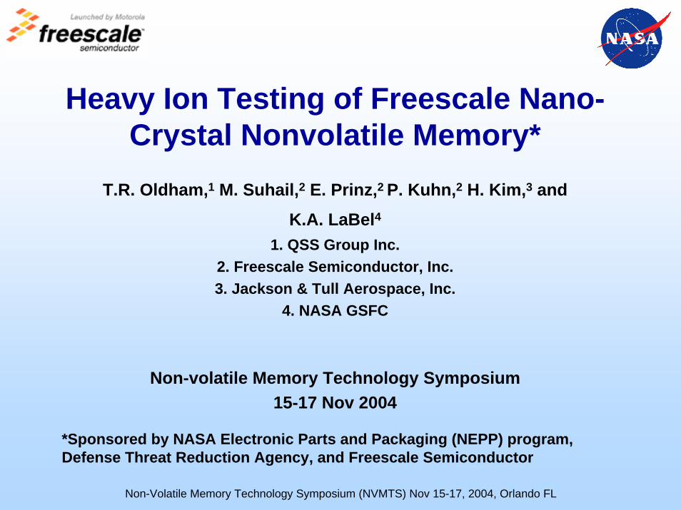
Non-Volatile Memory Technology Symposium (NVMTS) Nov 15-17, 2004, Orlando FL
Heavy Ion Testing of Freescale Nano-Crystal Nonvolatile Memory*
T.R. Oldham,1 M. Suhail,2 E. Prinz,2 P. Kuhn,2 H. Kim,3 and
K.A. LaBel41. QSS Group Inc.
2. Freescale Semiconductor, Inc.3. Jackson & Tull Aerospace, Inc.
4. NASA GSFC
Non-volatile Memory Technology Symposium15-17 Nov 2004
*Sponsored by NASA Electronic Parts and Packaging (NEPP) program, Defense Threat Reduction Agency, and Freescale Semiconductor
Non-Volatile Memory Technology Symposium (NVMTS) Nov 15-17, 2004, Orlando FL 2
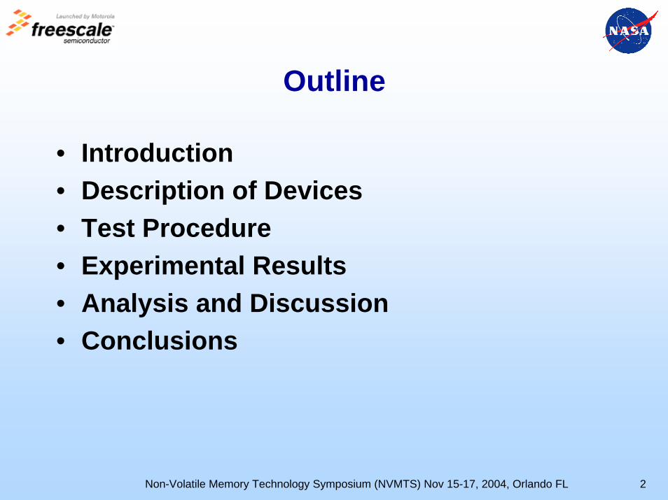
Outline
• Introduction • Description of Devices• Test Procedure• Experimental Results• Analysis and Discussion• Conclusions
Non-Volatile Memory Technology Symposium (NVMTS) Nov 15-17, 2004, Orlando FL 3
Introduction• Floating Gate (FG) non-volatile memories (NVM)
are widely used in space systems– Commercially available
• However,– FG has been shown to be sensitive to ionizing radiation– Concern that FG cannot be scaled below 100 nm for
reliability issues• Nanocrystal (NC) memory has the potential to
– Scale <<100 nm with increased reliability at 90 nm and below, as well as,
– Increase radiation resistance
Non-Volatile Memory Technology Symposium (NVMTS) Nov 15-17, 2004, Orlando FL 4
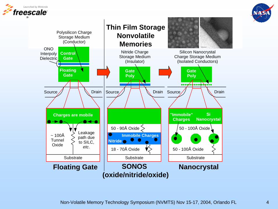
Floating Gate SONOS(oxide/nitride/oxide)
Nanocrystal
Thin Film StorageNonvolatileMemories
Source Drain
Substrate
50 - 100Å Oxide
50 - 100Å Oxide
SiNanocrystal
"Immobile"Charges
Silicon NanocrystalCharge Storage Medium
(Isolated Conductors)
GatePoly
Source Drain
FloatingGate
ControlGate
Leakagepath dueto SILC,
etc.
Substrate
~ 100ÅTunnelOxide
Charges are mobile
Polysilicon ChargeStorage Medium
(Conductor)
ONOInterpolyDielectric
Substrate
Nitride
50 - 90Å Oxide
18 - 70Å Oxide
Immobile Charges
Source Drain
Nitride ChargeStorage Medium
(Insulator)
GatePoly
Non-Volatile Memory Technology Symposium (NVMTS) Nov 15-17, 2004, Orlando FL 5
Nanocrystal Storage for Embedded NVM
• Write/Erase Voltage Reduction– ±6...±7V write/erase voltages instead of ±9V– 50% periphery area reduction
• No SILC (stress induced leakage current)-related extrinsic reliability issue
• No gate or drain coupling effect• Process Simplicity
– Floating gate: adds 6-11 masking steps– Nanocrystal: adds 4 masking steps
Non-Volatile Memory Technology Symposium (NVMTS) Nov 15-17, 2004, Orlando FL 6
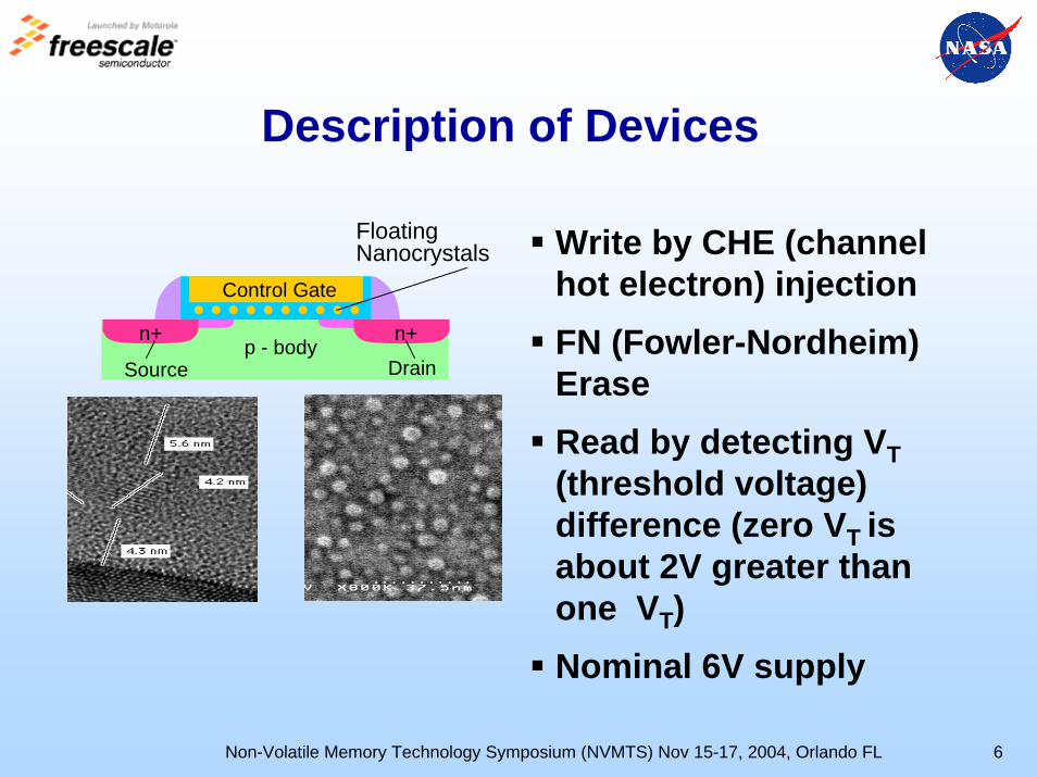
Description of Devices
Write by CHE (channel hot electron) injectionFN (Fowler-Nordheim) EraseRead by detecting VT (threshold voltage) difference (zero VT is about 2V greater than one VT)Nominal 6V supply
FloatingNanocrystals
Control Gate
p - bodySource Drain
n+ n+
Non-Volatile Memory Technology Symposium (NVMTS) Nov 15-17, 2004, Orlando FL 7
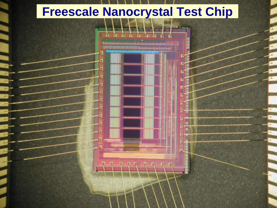
Freescale Nanocrystal Test Chip
Non-Volatile Memory Technology Symposium (NVMTS) Nov 15-17, 2004, Orlando FL 8
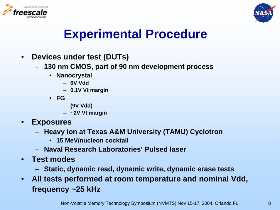
Experimental Procedure• Devices under test (DUTs)
– 130 nm CMOS, part of 90 nm development process• Nanocrystal
– 6V Vdd– 0.1V Vt margin
• FG– (9V Vdd)– ~2V Vt margin
• Exposures– Heavy ion at Texas A&M University (TAMU) Cyclotron
• 15 MeV/nucleon cocktail– Naval Research Laboratories’ Pulsed laser
• Test modes– Static, dynamic read, dynamic write, dynamic erase tests
• All tests performed at room temperature and nominal Vdd, frequency ~25 kHz
Non-Volatile Memory Technology Symposium (NVMTS) Nov 15-17, 2004, Orlando FL 9
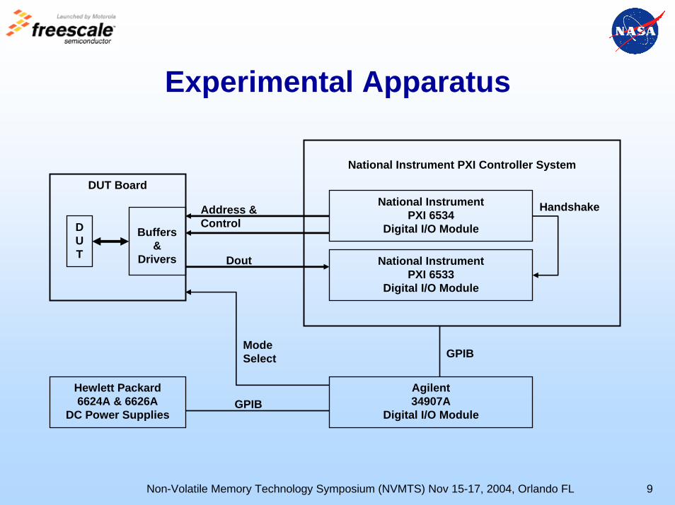
Experimental Apparatus
National Instrument PXI Controller System
DUT BoardNational Instrument
PXI 6534Digital I/O Module
Handshake
National InstrumentPXI 6533
Digital I/O Module
Address & ControlD
UT
Buffers &
Drivers Dout
Hewlett Packard6624A & 6626A
DC Power Supplies
Agilent34907A
Digital I/O Module
ModeSelect GPIB
GPIB
Non-Volatile Memory Technology Symposium (NVMTS) Nov 15-17, 2004, Orlando FL 10
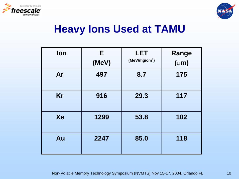
Heavy Ions Used at TAMU
Ion E(MeV)
LET(MeV/mg/cm2)
Range(µm)
Ar 497 8.7 175
Kr 916 29.3 117
Xe 1299 53.8 102
Au 2247 85.0 118
Non-Volatile Memory Technology Symposium (NVMTS) Nov 15-17, 2004, Orlando FL 11
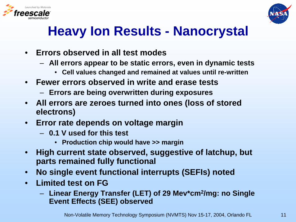
Heavy Ion Results - Nanocrystal• Errors observed in all test modes
– All errors appear to be static errors, even in dynamic tests• Cell values changed and remained at values until re-written
• Fewer errors observed in write and erase tests – Errors are being overwritten during exposures
• All errors are zeroes turned into ones (loss of stored electrons)
• Error rate depends on voltage margin – 0.1 V used for this test
• Production chip would have >> margin• High current state observed, suggestive of latchup, but
parts remained fully functional• No single event functional interrupts (SEFIs) noted• Limited test on FG
– Linear Energy Transfer (LET) of 29 Mev*cm2/mg: no Single Event Effects (SEE) observed
Non-Volatile Memory Technology Symposium (NVMTS) Nov 15-17, 2004, Orlando FL 12
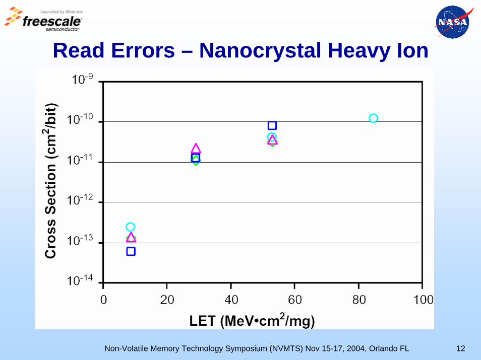
Read Errors – Nanocrystal Heavy Ion
Non-Volatile Memory Technology Symposium (NVMTS) Nov 15-17, 2004, Orlando FL 13
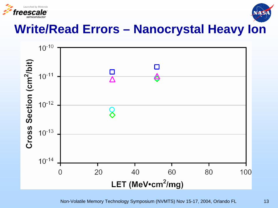
Write/Read Errors – Nanocrystal Heavy Ion
Non-Volatile Memory Technology Symposium (NVMTS) Nov 15-17, 2004, Orlando FL 14
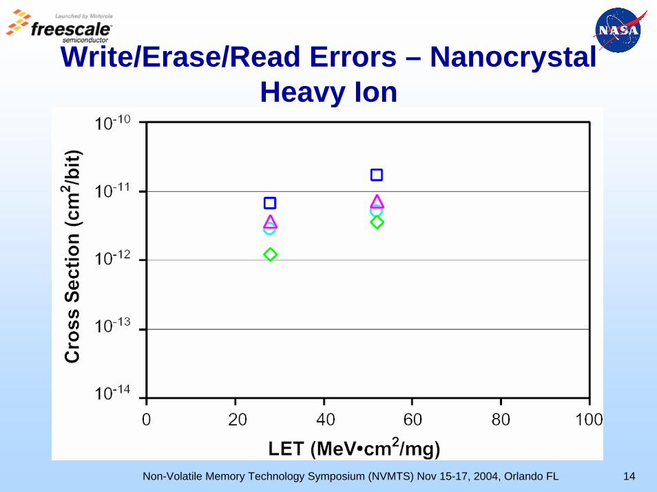
Write/Erase/Read Errors – NanocrystalHeavy Ion
Non-Volatile Memory Technology Symposium (NVMTS) Nov 15-17, 2004, Orlando FL 15
Laser Test Results – Nanocrystal and FG
• No bit errors observed– Laser will not produce ionization in SiO2
• No errors observed in control circuits on NC parts
• Apparent latchup in FG parts– Possibly due to higher voltages applied
• Devices could not be erased after exposure, including ultraviolet (UV) erase
Non-Volatile Memory Technology Symposium (NVMTS) Nov 15-17, 2004, Orlando FL 16
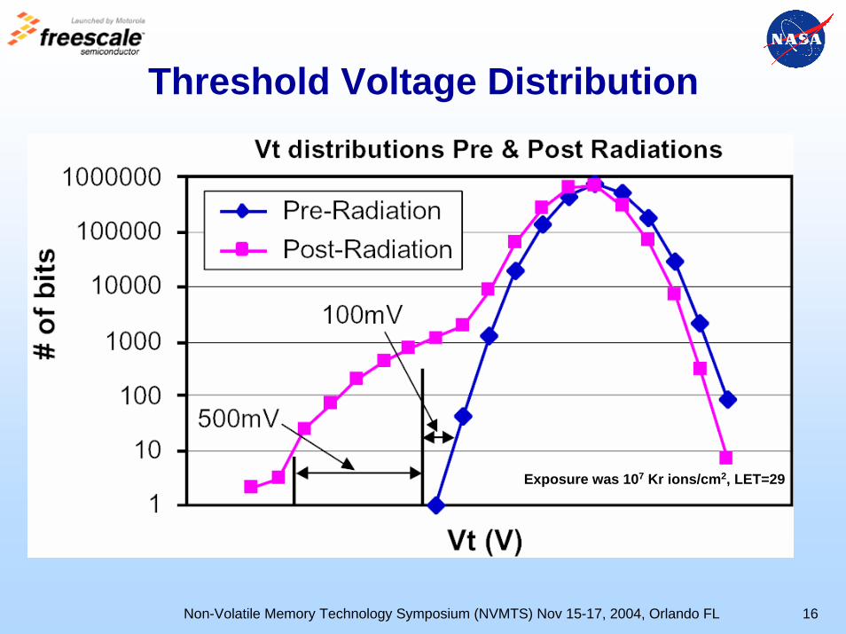
Threshold Voltage Distribution
Exposure was 107 Kr ions/cm2, LET=29
Non-Volatile Memory Technology Symposium (NVMTS) Nov 15-17, 2004, Orlando FL 17
Discussion• Charge loss, from observed VT shifts, is 1-2
orders of magnitude greater than positive charge deposited by ion– Micro-dose (alone) not sufficient to explain observed
charge loss• Cellere et al. (IEEE TNS Dec 2002) reported
similar results for FG cells—presented three possible models, but found problems with all three– Models should not apply to NC arrays, even if problems
were resolved for FG—single conducting defect should not drain charge from whole array
• Underlying mechanisms not yet explained
Non-Volatile Memory Technology Symposium (NVMTS) Nov 15-17, 2004, Orlando FL 18
Conclusions
• Nanocrystal memories are promising for space applications
• Bit error rate is generally better than previous reports for FG flash NVM
• Only static errors (loss of electrons) observed
• No SEFI• No unambiguous evidence for latchup