Embed Size (px)
Citation preview
Hendricks QRP KitsBITX20A
Assembly Manual
27 October 2007
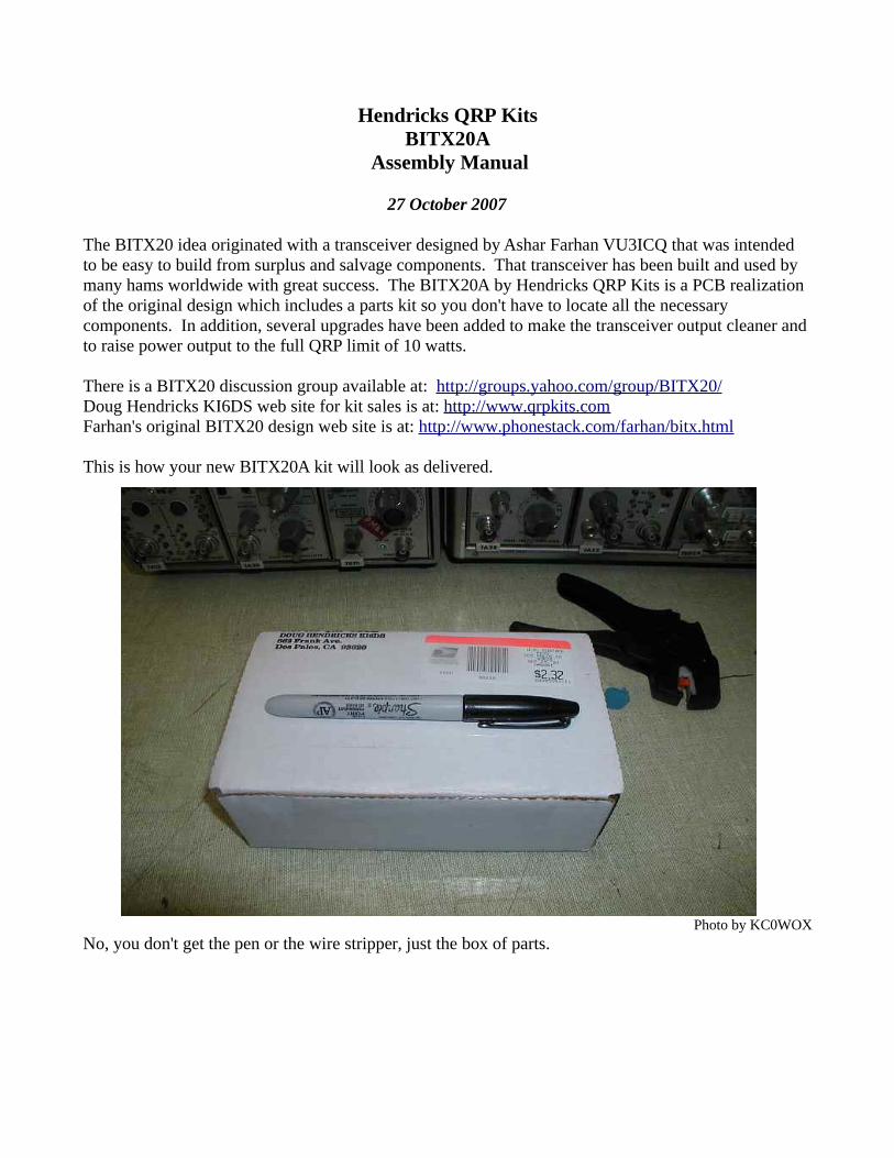
The BITX20 idea originated with a transceiver designed by Ashar Farhan VU3ICQ that was intended to be easy to build from surplus and salvage components. That transceiver has been built and used by many hams worldwide with great success. The BITX20A by Hendricks QRP Kits is a PCB realization of the original design which includes a parts kit so you don't have to locate all the necessary components. In addition, several upgrades have been added to make the transceiver output cleaner and to raise power output to the full QRP limit of 10 watts.
There is a BITX20 discussion group available at: http://groups.yahoo.com/group/BITX20/Doug Hendricks KI6DS web site for kit sales is at: http://www.qrpkits.comFarhan's original BITX20 design web site is at: http://www.phonestack.com/farhan/bitx.html
This is how your new BITX20A kit will look as delivered.
Photo by KC0WOXNo, you don't get the pen or the wire stripper, just the box of parts.
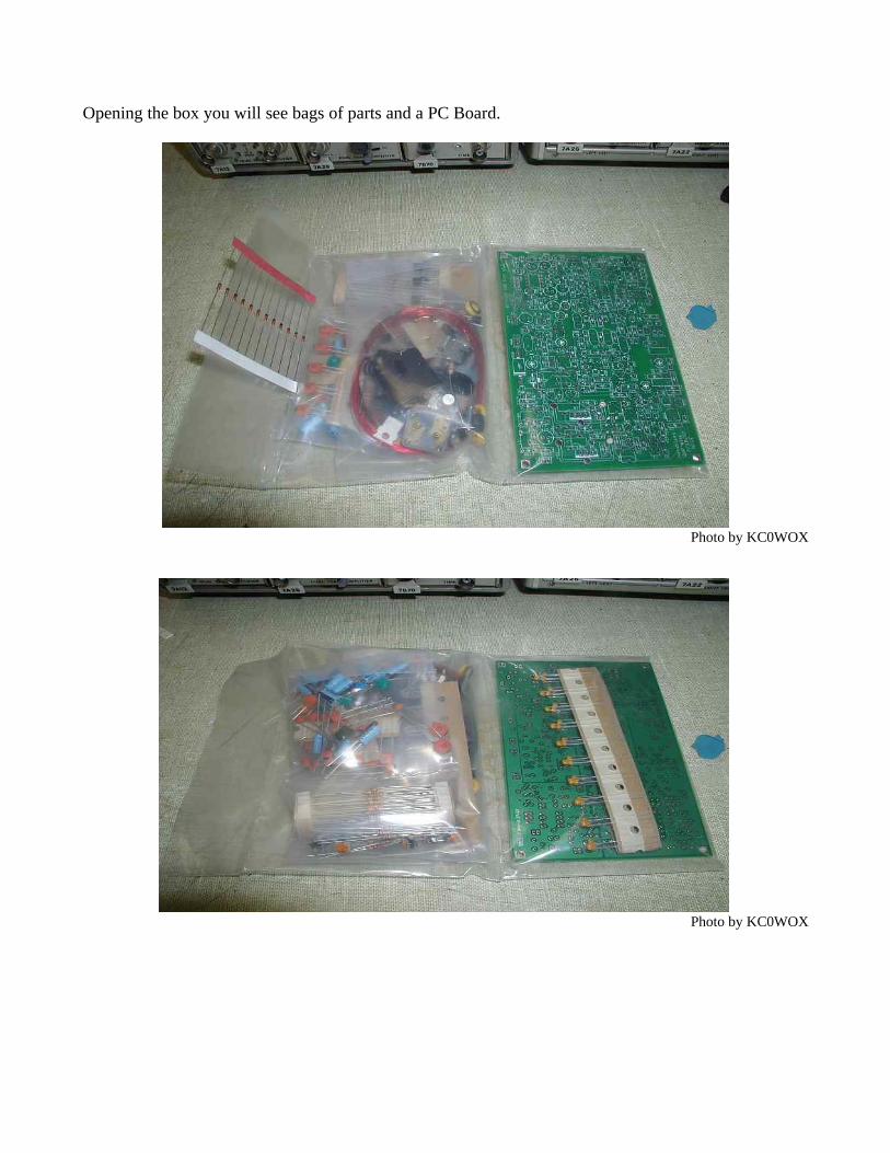
Opening the box you will see bags of parts and a PC Board.
Photo by KC0WOX
Photo by KC0WOX
Parts Inventory:
Quantity Value Device Quantity Value Device
1 160 pf External tuning cap 1 2.2 Resistors
5 10 uf POLARIZED CAP 1 4.7
7 100 uf POLARIZED CAP 9 10
1 220 pf POLYSTYRENE 2 22
2 470 pf POLYSTYRENE 13 100
4 30 pf Trim capacitor 14 220
2 470
1 0.01 uf 3 10K
40 0.1 uf 2 150 K
3 10 pf 15 1K
10 100 pf 11 2.2K
1 15 pf 1 2.7K
3 180 pf 1 22K
2 220 pf 1 3.3K
3 33 pf 11 4.7K
1 0.022 uf 5 11 MHz XTAL/S
2 56 pf Quantity Value Device
1 8.2 pf 1 33v ZENER_DO35_V
4 82 pf 1 5.6v ZENER_DO35_V
1 9.1v ZENER_DO35_V
1 1N4004 Diode
12 1N4148 Diode
Quantity Value Device Quantity Value Device
16 2N3904 Transistor 1 SB320 Diode
1 2N5486 Transistor 2 HEATSINK
4 2N7000 Transistor 1 RELAY
2 BS170 MOSFET
1 FQN1N50C MOSFET
1 LM386N-4 AF PA
2 IRF510 MOSFET Quantity Value Device
2 200 3318_TRIMMER 1 1.2 uH molded choke
3 10K 3318_TRIMMER 1 8.2 uH molded choke
1 10k Fine tune external pot 8 FT37-43 Toroid Core (Black)
1 10K Volume control external 5 T37-6 Toroids Core (Yellow)
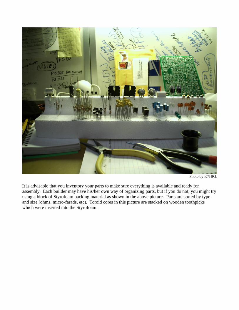
Photo by K7HKL
It is advisable that you inventory your parts to make sure everything is available and ready for assembly. Each builder may have his/her own way of organizing parts, but if you do not, you might try using a block of Styrofoam packing material as shown in the above picture. Parts are sorted by type and size (ohms, micro-farads, etc). Toroid cores in this picture are stacked on wooden toothpicks which were inserted into the Styrofoam.
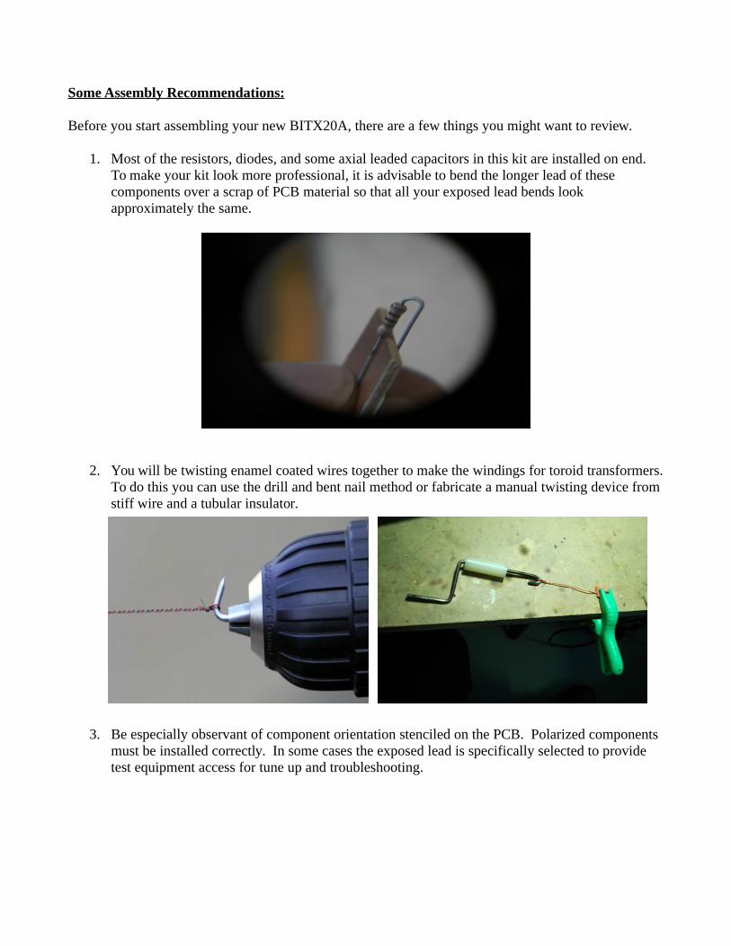
Some Assembly Recommendations:
Before you start assembling your new BITX20A, there are a few things you might want to review.
1. Most of the resistors, diodes, and some axial leaded capacitors in this kit are installed on end. To make your kit look more professional, it is advisable to bend the longer lead of these components over a scrap of PCB material so that all your exposed lead bends look approximately the same.
2. You will be twisting enamel coated wires together to make the windings for toroid transformers. To do this you can use the drill and bent nail method or fabricate a manual twisting device from stiff wire and a tubular insulator.
3. Be especially observant of component orientation stenciled on the PCB. Polarized components must be installed correctly. In some cases the exposed lead is specifically selected to provide test equipment access for tune up and troubleshooting.
Kit Assembly
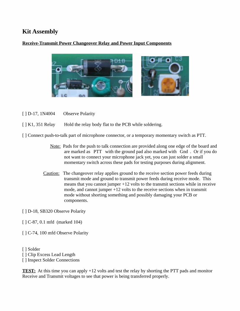
Receive-Transmit Power Changeover Relay and Power Input Components
[ ] D-17, 1N4004 Observe Polarity
[ ] K1, 351 Relay Hold the relay body flat to the PCB while soldering.
[ ] Connect push-to-talk part of microphone connector, or a temporary momentary switch as PTT.
Note: Pads for the push to talk connection are provided along one edge of the board andare marked as � PTT� with the ground pad also marked with � Gnd� . Or if you donot want to connect your microphone jack yet, you can just solder a small momentary switch across these pads for testing purposes during alignment.
Caution: The changeover relay applies ground to the receive section power feeds during transmit mode and ground to transmit power feeds during receive mode. This
means that you cannot jumper +12 volts to the transmit sections while in receivemode, and cannot jumper +12 volts to the receive sections when in transmit mode without shorting something and possibly damaging your PCB orcomponents.
[ ] D-18, SB320 Observe Polarity
[ ] C-87, 0.1 mfd (marked 104)
[ ] C-74, 100 mfd Observe Polarity
[ ] Solder[ ] Clip Excess Lead Length[ ] Inspect Solder Connections
TEST: At this time you can apply +12 volts and test the relay by shorting the PTT pads and monitor Receive and Transmit voltages to see that power is being transferred properly.
Receiver AF Amplifier
[ ] C-36, 100 mfd Observe Polarity
[ ] C-83, 0.1 mfd (marked � 104� )
[ ] R-81, 10 ohms (brown-black-black)
[ ] C-82, 10 mfd, Observe Polarity
[ ] IC-1, LM386, Make sure you get this positioned properly when you insert it.
[ ] Solder[ ] Clip Excess Lead Length[ ] Inspect Solder Connections
[ ] C86, 100 mfd, Observe Polarity
[ ] R-82, 10 ohms (brown-black-black)
[ ] R-79, 220 ohms (red-red-brown)
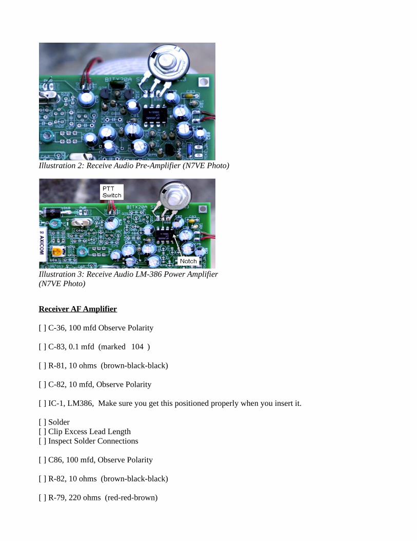
Illustration 2: Receive Audio Pre-Amplifier (N7VE Photo)
Illustration 3: Receive Audio LM-386 Power Amplifier (N7VE Photo)
[ ] R-80, 10K ohm potentiometer NOTE: Off-board component. Use 6 inch leads. Ground lead near C-82, Hot lead near Q-16.
[ ] C-81, 10 mfd Observe Polarity
[ ] C-80, 100 mfd Observe Polarity
[ ] R-78, 4.7K ohms (yellow-violet-red)
[ ] Solder[ ] Clip Excess Lead Length[ ] Inspect Solder Connections
[ ] Q-16, 2N3904 (Position as stenciled on the PCB)
[ ] Q-25, 2N3904 (Position as stenciled on the PCB)
[ ] R-88, 4.7K ohms, (yellow-violet-red)
[ ] R-89, 22K ohms (red-red-orange)
[ ] C-47, 0 pf (This is an artifact from an older PCB design. Do not install any capacitor here.)
[ ] C-79, 0.022 mfd (marked 22K)
[ ] R-77, 3.3K ohms (orange-orange-red)
[ ] C-8, 10 mfd Observe Polarity
[ ] Speaker or Headphone Jack Connection. Use 6 inch leads. Ground is the pad near C-75.
[ ] Solder[ ] Clip Excess Lead Length[ ] Inspect Solder Connections
TEST: At this point you can test your receiver audio amplifier by connecting a speaker, applying +12 volts to the power input pads. Insert a tone at the negative side of C8, and adjust the volume control for a comfortable listening level.
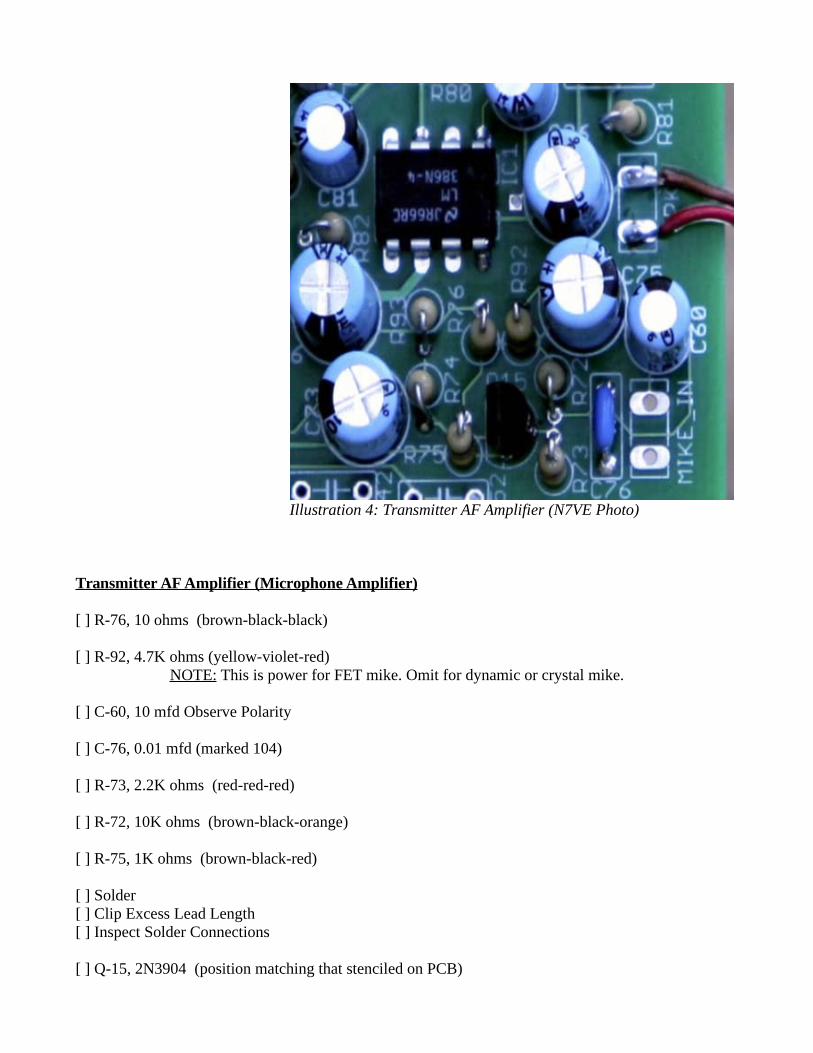
Transmitter AF Amplifier (Microphone Amplifier)
[ ] R-76, 10 ohms (brown-black-black)
[ ] R-92, 4.7K ohms (yellow-violet-red) NOTE: This is power for FET mike. Omit for dynamic or crystal mike.
[ ] C-60, 10 mfd Observe Polarity
[ ] C-76, 0.01 mfd (marked 104)
[ ] R-73, 2.2K ohms (red-red-red)
[ ] R-72, 10K ohms (brown-black-orange)
[ ] R-75, 1K ohms (brown-black-red)
[ ] Solder[ ] Clip Excess Lead Length[ ] Inspect Solder Connections
[ ] Q-15, 2N3904 (position matching that stenciled on PCB)
Illustration 4: Transmitter AF Amplifier (N7VE Photo)
[ ] R-74, 100 ohms (brown-black-brown)
[ ] C-73, 100 mfd Observe Polarity
[ ] R-93, 220 ohms (red-red-brown)
[ ] C-77, 10 mfd Observe Polarity
[ ] C-75, 100 mfd Observe Polarity
[ ] Solder[ ] Clip Excess Lead Length[ ] Inspect Solder Connections
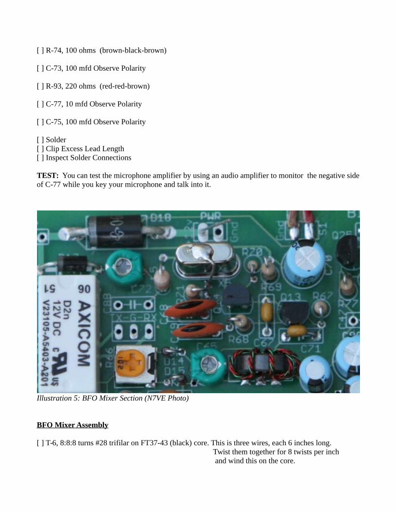
TEST: You can test the microphone amplifier by using an audio amplifier to monitor the negative side of C-77 while you key your microphone and talk into it.
BFO Mixer Assembly
[ ] T-6, 8:8:8 turns #28 trifilar on FT37-43 (black) core. This is three wires, each 6 inches long. Twist them together for 8 twists per inch and wind this on the core.
Illustration 5: BFO Mixer Section (N7VE Photo)
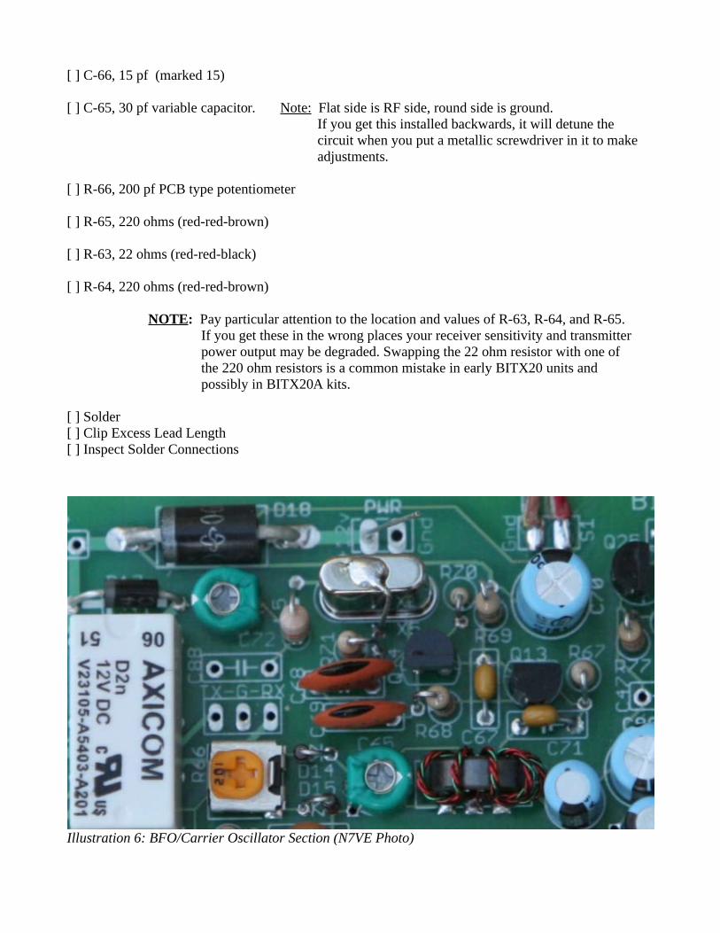
[ ] C-66, 15 pf (marked 15)
[ ] C-65, 30 pf variable capacitor. Note: Flat side is RF side, round side is ground.If you get this installed backwards, it will detune the circuit when you put a metallic screwdriver in it to makeadjustments.
[ ] R-66, 200 pf PCB type potentiometer
[ ] R-65, 220 ohms (red-red-brown)
[ ] R-63, 22 ohms (red-red-black)
[ ] R-64, 220 ohms (red-red-brown)
NOTE: Pay particular attention to the location and values of R-63, R-64, and R-65. If you get these in the wrong places your receiver sensitivity and transmitter power output may be degraded. Swapping the 22 ohm resistor with one of the 220 ohm resistors is a common mistake in early BITX20 units and possibly in BITX20A kits.
[ ] Solder[ ] Clip Excess Lead Length[ ] Inspect Solder Connections
Illustration 6: BFO/Carrier Oscillator Section (N7VE Photo)
BFO & Carrier Oscillator
[ ] C-88, 33 pf NOTE: May not be needed, but provided to insure adequate tuning range.
[ ] C-72, 30 pf variable capacitor, Note: flat side is RF side, round side is ground.
[ ] L-5, 8.2 uh molded inductor (looks like a fat resistor with gray-red-gold-gold bands)
[ ] X-5, 11.0 MHz Crystal. [ ] Add ground wire soldered to crystal case
[ ] C-68, 220 pf (marked 221)
[ ] C-69, 220 pf (marked 221)
[ ] R-70, 150K ohms (marked brown-green-yellow)
[ ] Solder[ ] Clip Excess Lead Length[ ] Inspect Solder Connections
[ ] Q-14, 2N3904 (Position according to layout stenciled on PCB)
[ ] R-71, 1K ohms (brown-black-red)
[ ] C-70, 100 mfd Observe Polarity
[ ] R-69, 100 ohms (brown-black-brown)
[ ] R-68, 1K ohms (brown-black-brown)
[ ] Q-13, 2N3904 (Position according to layout stenciled on PCB)
[ ] Solder[ ] Clip Excess Lead Length[ ] Inspect Solder Connections
[ ] C-67, 0.1 mfd (marked 104)
[ ] C-71, 0.1 mfd (marked 104)
[ ] R-67, 1K ohms (brown-black-red)
[ ] D-14, 1N4148 Observe Polarity
[ ] D-15, 1N4148 Observe Polarity
[ ] Solder[ ] Clip Excess Lead Length

[ ] Inspect Solder Connections
TEST: Insert an 11.0 MHz signal across R-64 and listen for a beat-note from the receive audio amplifier.
Receive 2nd IF Amp and Transmit 1st IF Amp
[ ] C-64, 0.1 mfd (marked 104)
[ ] R-58, 1K ohms (brown-black-red)
[ ] R-57, 2.2K ohms (red-red-red)
[ ] Q-12, 2N3904 (Position according to marking stenciled on PCB)
[ ] R-60, 4.7 ohms (yellow-violet-black)
[ ] C-61, 0.1 mfd (marked 104)
[ ] R-59, 470 ohms (yellow-violet-brown)
[ ] Solder[ ] Clip Excess Lead Length[ ] Inspect Solder Connections
[ ] D-13, 1N4148 Observe Polarity
Illustration 7: Second IF Amp Section (N7VE Photo)
[ ] R-61, 220 ohms (red-red-brown)
[ ] C-63, 0.1 mfd (marked 104)
[ ] R-62, 100 ohms (brown-black-brown)
[ ] R-56, 100 ohms (brown-black-brown)
[ ] C-57, 0.1 mfd (marked 104)
[ ] D-12, 1N4148 Observe Polarity
[ ] Q-17, 2N3904 (Position according to layout stenciled on PCB)
[ ] Solder[ ] Clip Excess Lead Length[ ] Inspect Solder Connections
[ ] C-58, 0.1 mfd (marked 104)
[ ] R-53, 470 ohms (yellow-violet-brown)
[ ] R-55, 4.7K ohms (yellow-violet-red)
[ ] R-52, 1K ohms (brown-black-red)
[ ] Q-11, 2N3904 (Position according to markings stenciled on PCB)
[ ] Solder[ ] Clip Excess Lead Length[ ] Inspect Solder Connections
[ ] R-54, 4.7K ohms (yellow-violet-red)
[ ] C-59, 0.1 mfd (marked 104)
[ ] R-51, 220 ohms (red-red-brown)
[ ] C-89, 100 pf (marked 101)
[ ] C-62, 100 pf (marked 101)
[ ] Solder[ ] Clip Excess Lead Length[ ] Inspect Solder Connections
TEST: Insert an 11.0 MHz signal at the junction of C-62 and C-89, and listen for a beat-note from the receive audio amplifier.
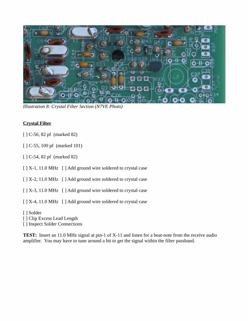
Crystal Filter
[ ] C-56, 82 pf (marked 82)
[ ] C-55, 100 pf (marked 101)
[ ] C-54, 82 pf (marked 82)
[ ] X-1, 11.0 MHz [ ] Add ground wire soldered to crystal case
[ ] X-2, 11.0 MHz [ ] Add ground wire soldered to crystal case
[ ] X-3, 11.0 MHz [ ] Add ground wire soldered to crystal case
[ ] X-4, 11.0 MHz [ ] Add ground wire soldered to crystal case
[ ] Solder[ ] Clip Excess Lead Length[ ] Inspect Solder Connections
TEST: Insert an 11.0 MHz signal at pin-1 of X-11 and listen for a beat-note from the receive audio amplifier. You may have to tune around a bit to get the signal within the filter passband.
Illustration 8: Crystal Filter Section (N7VE Photo)
Receiver 1st IF and Transmitter 2nd IF
[ ] C-53, 100 pf (marked 101)
[ ] R-46, 1K ohms (brown-black-red)
[ ] R-45, 2.2K ohms (red-red-red)
[ ] Q-10, 2N3904 (Position according to layour marked on PCB)
[ ] R-48, 10 ohms (brown-black-black)
[ ] C-44, 0.1 mfd (marked 104)
[ ] Solder[ ] Clip Excess Lead Length[ ] Inspect Solder Connections
[ ] R-47, 220 ohms (red-red-brown)
[ ] D-11, 1N4148 Observe Polarity
[ ] R-49, 220 ohms (red-red-brown)
[ ] C-45, 0.1 mfd (marked 104)
[ ] C-46, 0.1 mfd (marked 104)
[ ] R-50, 100 ohms (brown-black-brown)
[ ] Solder
Illustration 9: Receiver First IF and Transmitter Second IF (N7VE Photo)
[ ] Clip Excess Lead Length[ ] Inspect Solder Connections
[ ] C-52, 100 pf (marked 101)
[ ] D-10, 1N4148 Observe Polarity
[ ] R-43, 220 ohms (red-red-brown)
[ ] C-42, 0.1 mfd (marked 104)
[ ] R-44, 100 ohms (brown-black-brown)
[ ] Q-9, 2N3904 (Position according to layout marked on PCB)
[ ] R-39, 2.2K ohms (red-red-red)
[ ] C-43, 0.1 mfd (marked 104)
[ ] R-40, 1K ohms (brown-black-red)
[ ] R-41, 220 ohms (red-red-brown)
[ ] R-42, 10 ohms (brown-black-black)
[ ] C-40, 0.1 mfd (marked 104)
[ ] Solder[ ] Clip Excess Lead Length[ ] Inspect Solder Connections
TEST: Insert an 11.0 MHz signal at the junction of C-43 and C-45, and listen for a beat-note from the receive audio amplifier.
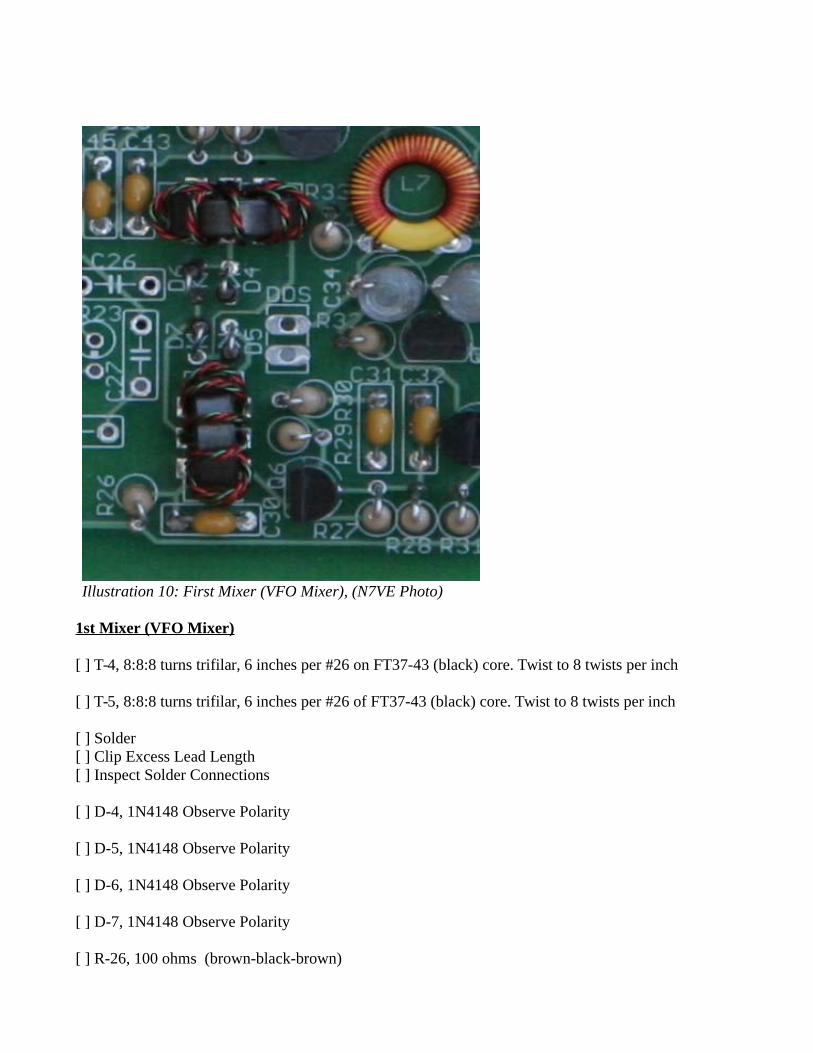
1st Mixer (VFO Mixer)
[ ] T-4, 8:8:8 turns trifilar, 6 inches per #26 on FT37-43 (black) core. Twist to 8 twists per inch
[ ] T-5, 8:8:8 turns trifilar, 6 inches per #26 of FT37-43 (black) core. Twist to 8 twists per inch
[ ] Solder[ ] Clip Excess Lead Length[ ] Inspect Solder Connections
[ ] D-4, 1N4148 Observe Polarity
[ ] D-5, 1N4148 Observe Polarity
[ ] D-6, 1N4148 Observe Polarity
[ ] D-7, 1N4148 Observe Polarity
[ ] R-26, 100 ohms (brown-black-brown)
Illustration 10: First Mixer (VFO Mixer), (N7VE Photo)
[ ] C-30, 0.1 mfd (marked 104)
[ ] Solder[ ] Clip Excess Lead Length[ ] Inspect Solder Connections
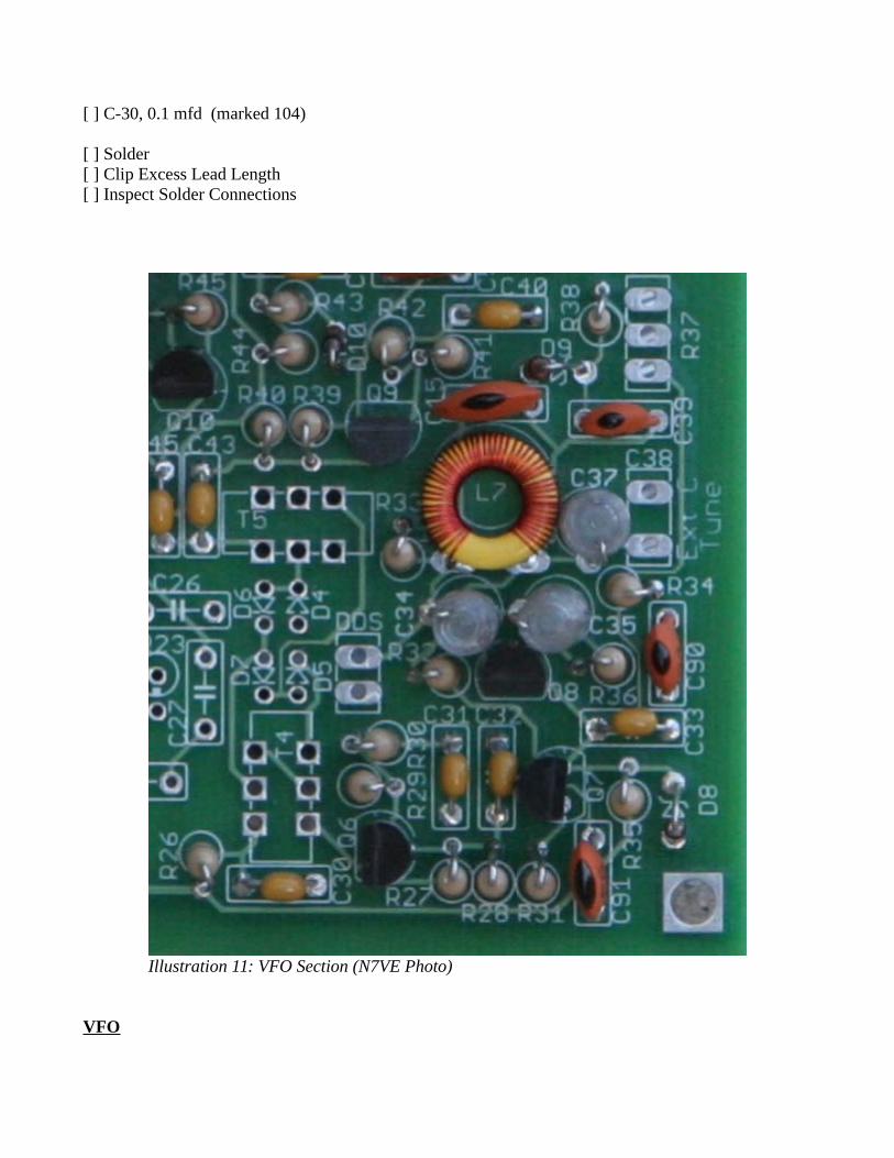
VFO
Illustration 11: VFO Section (N7VE Photo)
[ ] R-35, 100 ohms (brown-black-brown)
[ ] D-8, 1N4739A, 9.1 Volt Zener Observe Polarity
[ ] R-33, 10K ohms (brown-black-orange)
[ ] R-34, 10K ohms (brown-black-orange)
[ ] C-33, 0.1 mfd (marked 104)
[ ] Solder[ ] Clip Excess Lead Length[ ] Inspect Solder Connections
[ ] Q-8, 2N3904 (position according to layout marking on PCB)
[ ] Q-7, 2N3904 (position according to layout marking on PCB)
[ ] Q-6, 2N3904 (position according to layout marking on PCB)
[ ] Solder[ ] Clip Excess Lead Length[ ] Inspect Solder Connections
[ ] R-31, 1K ohms (brown-black-red)
[ ] C-32, 0.1 mfd (marked 104
[ ] R-28, 1K ohms (brown-black-red)
[ ] R-27, 1K ohms (brown-black-red)
[ ] R-30, 10 ohms (brown-black-black)
[ ] R-29, 100 ohms (brown-black-brown)
[ ] C-31, 0.1 mfd (marked 104)
[ ] Solder[ ] Clip Excess Lead Length[ ] Inspect Solder Connections
[ ] R-36, 2.2K ohms (red-red-red)
[ ] C-90, 33 pf (marked 33)
[ ] C-35, 470 pf Polystyrene (marked 470) NOTE: Polystyrene caps are encased in clear plastic.
[ ] C-34, 470 pf Polystyrene (marked 470) NOTE: Polystyrene caps are encased in clear plastic.
[ ] C-15, 180 pf (marked 180)
[ ] C-37, 220 pf Polystyrene (marked 220) NOTE: Polystyrene caps are encased in clear plastic.
[ ] C-39, 33 pf (marked 33)
[ ] R-32, 4700 ohms (yellow-violet-red)
[ ] C-91, 56 pf (marked 56)
[ ] D-9, 1N4752A, 33 Volt Zener (used as fine tuning varicap) Observe Polarity
[ ] Solder[ ] Clip Excess Lead Length[ ] Inspect Solder Connections
[ ] R-38, 150K ohms (brown-green-yellow)
[ ] L-7, 50 turns #36 on T-37-6 (yellow) core
Note: Do not secure L-7 to the PCB until you are sure that you have the desired tuning range. You may have to add or delete a turn if you want something other than the standard tuning range.Once you are sure you have the proper tuning rangeyou can secure the VFO inductor by cutting a smallscrap of hot-melt glue, placing that inside the toroidand melting it with the tip of your soldering iron. Besure to wipe the iron tip soon afterward or it will smell like baked hot-melt glue.
[ ] C-38, 160 pf Variable Capacitor. Polyvaricon used as main tuning. This is a front panel controland needs to be mounted on fairly stiff leads to minimize thepotential for vibration.
NOTE: You can control your tuning range by selection of which capacitor sections you use:
Polyvaricon Trimmer Open Trimmer Closed Section-A 60 kHz 58 kHz Section-B 124 kHz 120 kHz Sections A+B 155 kHz 147 kHz
[ ] R-37, 10K Potentiometer. This is the fine tuning adjustment.
[ ] Solder[ ] Clip Excess Lead Length[ ] Inspect Solder Connections
TEST: Monitor the VFO frequency on a counter or with a receiver that is capable of tuning 3.0 to 3.5 MHz.
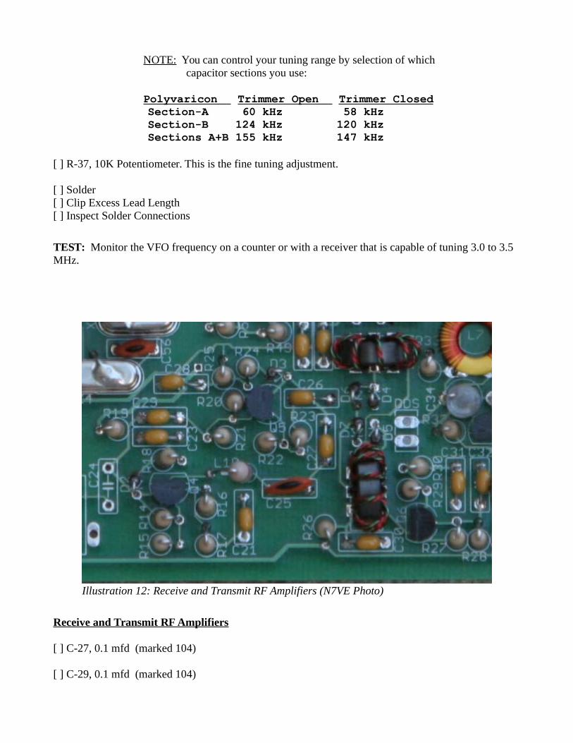
Receive and Transmit RF Amplifiers
[ ] C-27, 0.1 mfd (marked 104)
[ ] C-29, 0.1 mfd (marked 104)
Illustration 12: Receive and Transmit RF Amplifiers (N7VE Photo)
[ ] R-20, 2.2K ohms (red-red-red)
[ ] R-21, 1K ohms (brown-black-brown)
[ ] R-23, 10 ohms (brown-black-black)
[ ] R-22, 220 ohms (red-red-brown)
[ ] C-26, 0.1 mfd (marked 104)
[ ] Solder[ ] Clip Excess Lead Length[ ] Inspect Solder Connections
[ ] Q-5, 2N3904 (position according to layout stenciled on PCB)
[ ] D-3, 1N4148 Observe Polarity
[ ] R-24, 220 ohms (red-red-brown)
[ ] R-25, 100 ohms (brown-black-brown)
[ ] C-28, 0.1 mfd (marked 104)
[ ] Solder[ ] Clip Excess Lead Length[ ] Inspect Solder Connections
[ ] D-2, 1N4148 Observe Polarity
[ ] R-18, 220 ohms (red-red-brown)
[ ] C-23, 0.1 mfd (marked 104)
[ ] R-19, 100 ohms (brown-black-brown)
[ ] R-16, 220 ohms (red-red-brown)
[ ] R-17, 10 ohms (brown-black-black)
[ ] C-21, 0.1 mfd (marked 104)
[ ] Solder[ ] Clip Excess Lead Length[ ] Inspect Solder Connections
[ ] R-14, 2.2K ohms (red-red-red)
[ ] Q-4, 2N3904 (position according to layout marked on PCB)
[ ] R-15, 1K ohms (brown-black-red)
[ ] L-10, 1.2 uh molded inductor (brown-red-gold-gold) It looks like a fat resistor.
[ ] C-25, 100 pf (marked 101)
[ ] Solder[ ] Clip Excess Lead Length[ ] Inspect Solder Connections
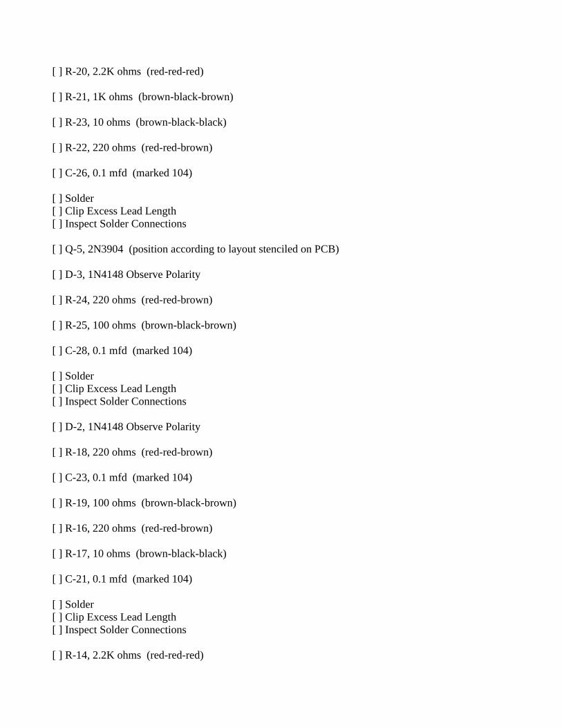
Receive and Transmit Front End Filter
[ ] C-24, 8.2 pf (marked 8.2)
[ ] L-6, 18 turns (20 inches) #26 on T-37-6 (yellow) core
[ ] C-18, 30 pf Observe Polarity
NOTE: The rounded side connects to ground and the flat side to RF
[ ] C-20, 82 pf (marked 82)
[ ] Solder[ ] Clip Excess Lead Length[ ] Inspect Solder Connections
[ ] C-19, 10 pf (marked 10)
[ ] C-17, 56 pf (marked 56)
[ ] C-16, 10 pf (marked 10)
[ ] L-4, 18 turns (20 inches) #26 on T-37-6 (yellow) core
[ ] Solder[ ] Clip Excess Lead Length[ ] Inspect Solder Connections
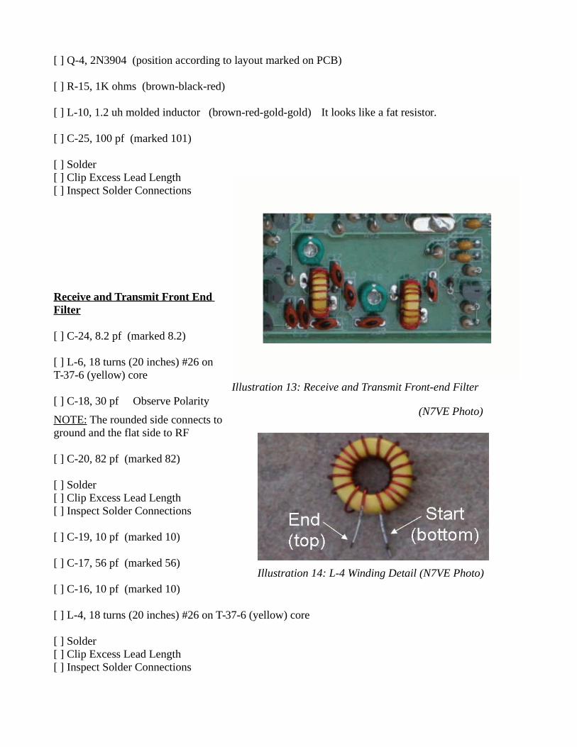
Illustration 14: L-4 Winding Detail (N7VE Photo)
Illustration 13: Receive and Transmit Front-end Filter
(N7VE Photo)
[ ] C-14, 30 pf Install this capacitor according to outline stenciled on the PCB
NOTE: The rounded side connects to ground and the flat side to RF
[ ] C-13, 82 pf (marked 82)
[ ] C-11, 10 pf (marked 10)
[ ] Solder[ ] Clip Excess Lead Length[ ] Inspect Solder Connections
TEST: Connect an antenna to C-11 and tune the VFO for received signals.
NOTE: Testing of the TR Switches, Transmit Drivers, and Transmit PA will be done as part of the alignment process after wiring is completed.
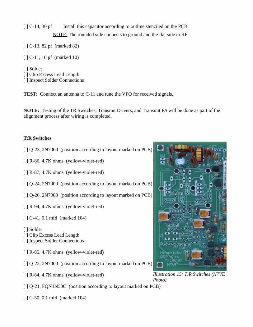
T:R Switches
[ ] Q-23, 2N7000 (position according to layout marked on PCB)
[ ] R-86, 4.7K ohms (yellow-violet-red)
[ ] R-87, 4.7K ohms (yellow-violet-red)
[ ] Q-24, 2N7000 (position according to layout marked on PCB)
[ ] Q-26, 2N7000 (position according to layout marked on PCB)
[ ] R-94, 4.7K ohms (yellow-violet-red)
[ ] C-41, 0.1 mfd (marked 104)
[ ] Solder[ ] Clip Excess Lead Length[ ] Inspect Solder Connections
[ ] R-85, 4.7K ohms (yellow-violet-red)
[ ] Q-22, 2N7000 (position according to layout marked on PCB)
[ ] R-84, 4.7K ohms (yellow-violet-red)
[ ] Q-21, FQN1N50C (position according to layout marked on PCB)
[ ] C-50, 0.1 mfd (marked 104)
Illustration 15: T:R Switches (N7VE Photo)
[ ] Solder[ ] Clip Excess Lead Length[ ] Inspect Solder Connections
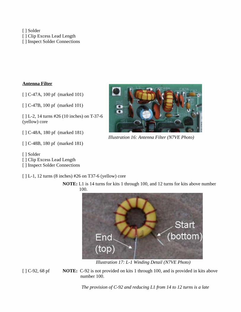
Antenna Filter
[ ] C-47A, 100 pf (marked 101)
[ ] C-47B, 100 pf (marked 101)
[ ] L-2, 14 turns #26 (10 inches) on T-37-6 (yellow) core
[ ] C-48A, 180 pf (marked 181)
[ ] C-48B, 180 pf (marked 181)
[ ] Solder[ ] Clip Excess Lead Length[ ] Inspect Solder Connections
[ ] L-1, 12 turns (8 inches) #26 on T37-6 (yellow) core
NOTE: L1 is 14 turns for kits 1 through 100, and 12 turns for kits above number 100.
[ ] C-92, 68 pf NOTE: C-92 is not provided on kits 1 through 100, and is provided in kits above number 100.
The provision of C-92 and reducing L1 from 14 to 12 turns is a late
Illustration 16: Antenna Filter (N7VE Photo)
Illustration 17: L-1 Winding Detail (N7VE Photo)
change that provided additional harmonic reduction.
[ ] C-49B, 100 pf (marked 101)
[ ] C-49A, 100 pf (marked 101)
[ ] Solder[ ] Clip Excess Lead Length[ ] Inspect Solder Connections
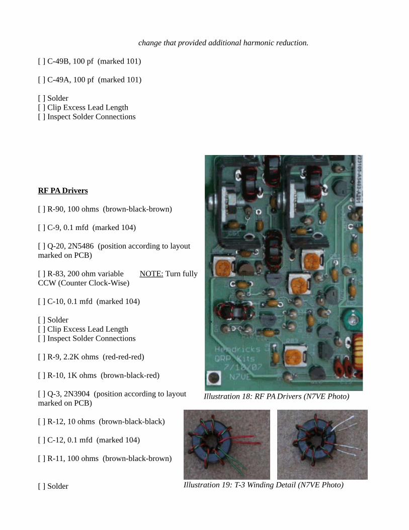
RF PA Drivers
[ ] R-90, 100 ohms (brown-black-brown)
[ ] C-9, 0.1 mfd (marked 104)
[ ] Q-20, 2N5486 (position according to layout marked on PCB)
[ ] R-83, 200 ohm variable NOTE: Turn fully CCW (Counter Clock-Wise)
[ ] C-10, 0.1 mfd (marked 104)
[ ] Solder[ ] Clip Excess Lead Length[ ] Inspect Solder Connections
[ ] R-9, 2.2K ohms (red-red-red)
[ ] R-10, 1K ohms (brown-black-red)
[ ] Q-3, 2N3904 (position according to layout marked on PCB)
[ ] R-12, 10 ohms (brown-black-black)
[ ] C-12, 0.1 mfd (marked 104)
[ ] R-11, 100 ohms (brown-black-brown)
[ ] Solder
Illustration 18: RF PA Drivers (N7VE Photo)
Illustration 19: T-3 Winding Detail (N7VE Photo)
[ ] Clip Excess Lead Length[ ] Inspect Solder Connections
[ ] R-13, 22 ohms (red-red-black)
[ ] C-6, 0.1 mfd (marked 104)
[ ] T-3, 8:8 turns (6 inches each lead) bifilar on #26 on FT37-43, (black) core. Twist to 8 turns per inch
[ ] R-5, 2.2K ohms (red-red-red)
[ ] R-6, 2.2K ohms (red-red-red)
[ ] C-4, 0.1 mfd (marked 104)
[ ] R-8, 10K potentiometer NOTE: Turn fully CCW
[ ] Solder[ ] Clip Excess Lead Length[ ] Inspect Solder Connections
[ ] Q-18, BS170 (position according to layout marked on PCB)
[ ] Q-19, BS170 (position according to layout marked on PCB)
[ ] R-7, 2.2 ohms (red-red-gold)
[ ] C-7, 0.1 mfd (marked 104)
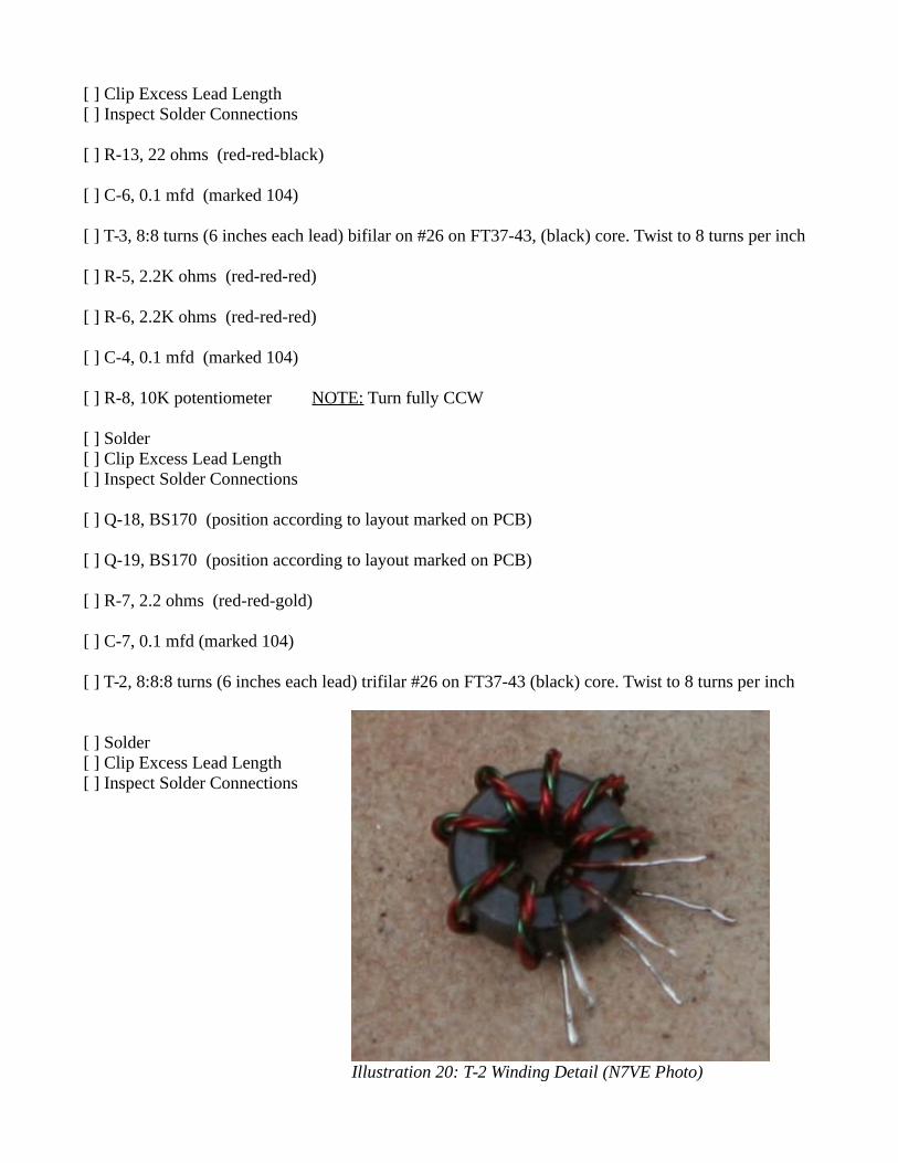
[ ] T-2, 8:8:8 turns (6 inches each lead) trifilar #26 on FT37-43 (black) core. Twist to 8 turns per inch
[ ] Solder[ ] Clip Excess Lead Length[ ] Inspect Solder Connections
Illustration 20: T-2 Winding Detail (N7VE Photo)
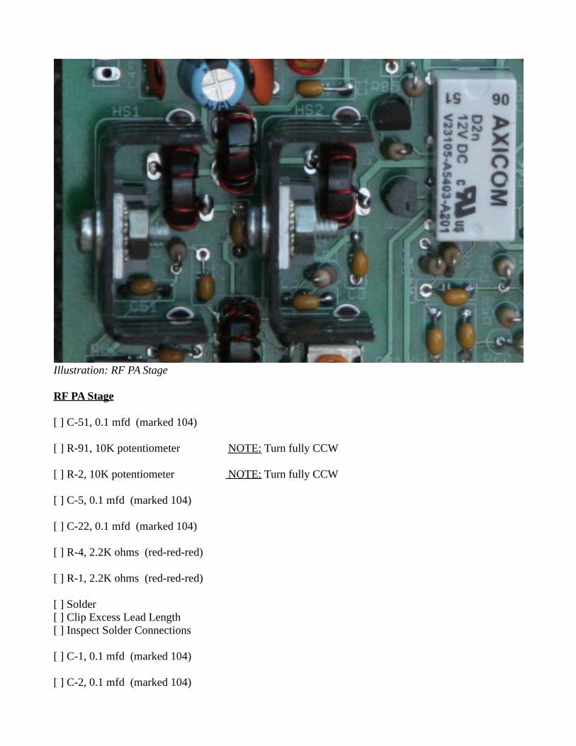
RF PA Stage
[ ] C-51, 0.1 mfd (marked 104)
[ ] R-91, 10K potentiometer NOTE: Turn fully CCW
[ ] R-2, 10K potentiometer NOTE: Turn fully CCW
[ ] C-5, 0.1 mfd (marked 104)
[ ] C-22, 0.1 mfd (marked 104)
[ ] R-4, 2.2K ohms (red-red-red)
[ ] R-1, 2.2K ohms (red-red-red)
[ ] Solder[ ] Clip Excess Lead Length[ ] Inspect Solder Connections
[ ] C-1, 0.1 mfd (marked 104)
[ ] C-2, 0.1 mfd (marked 104)
Illustration: RF PA Stage
[ ] C-3, 0.1 mfd (marked 104)
[ ] D-1, 1N4734A 5.6 Volt Zener Observe Polarity
[ ] R-3, 1K ohms (brown-black-red)
[ ] Solder[ ] Clip Excess Lead Length[ ] Inspect Solder Connections
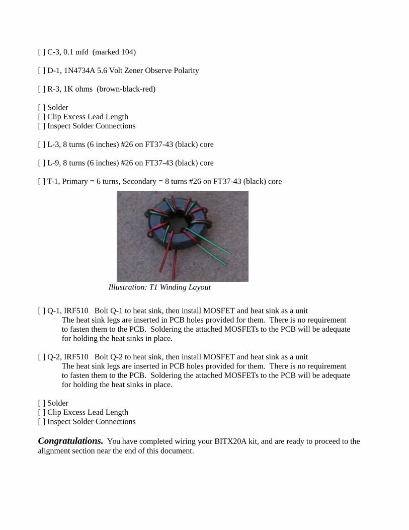
[ ] L-3, 8 turns (6 inches) #26 on FT37-43 (black) core
[ ] L-9, 8 turns (6 inches) #26 on FT37-43 (black) core
[ ] T-1, Primary = 6 turns, Secondary = 8 turns #26 on FT37-43 (black) core
[ ] Q-1, IRF510 Bolt Q-1 to heat sink, then install MOSFET and heat sink as a unitThe heat sink legs are inserted in PCB holes provided for them. There is no requirement to fasten them to the PCB. Soldering the attached MOSFETs to the PCB will be adequatefor holding the heat sinks in place.
[ ] Q-2, IRF510 Bolt Q-2 to heat sink, then install MOSFET and heat sink as a unitThe heat sink legs are inserted in PCB holes provided for them. There is no requirement to fasten them to the PCB. Soldering the attached MOSFETs to the PCB will be adequatefor holding the heat sinks in place.
[ ] Solder[ ] Clip Excess Lead Length[ ] Inspect Solder Connections
Congratulations. You have completed wiring your BITX20A kit, and are ready to proceed to the alignment section near the end of this document.
Illustration: T1 Winding Layout
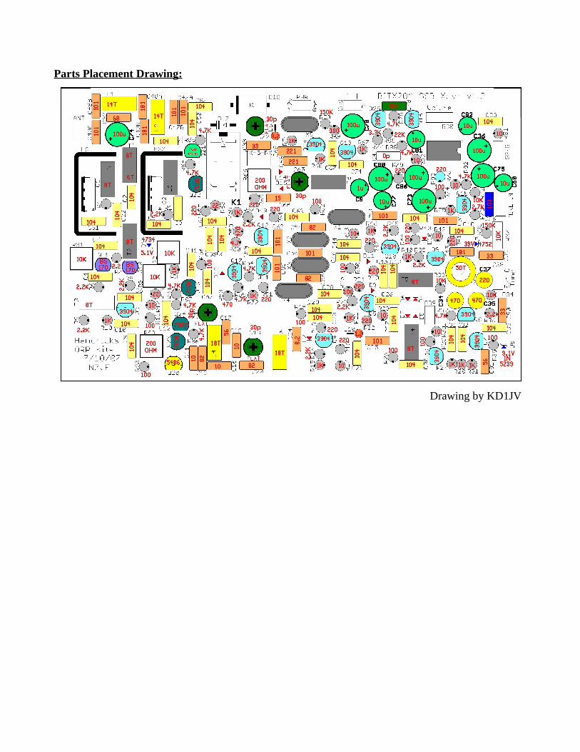
Parts Placement Drawing:
Drawing by KD1JV
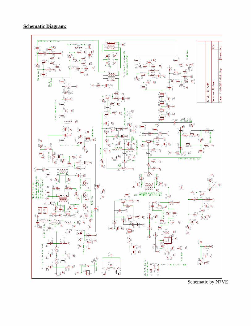
Schematic Diagram:
Schematic by N7VE
Alignment Method:
BFO/Carrier Oscillator:There are several ways to adjust the BFO/Carrier Oscillator frequency.
1. Rough alignment may be made by adjusting C-72 while listening to a received SSB signal on 20 meters. This is a two-handed operation as you have to use the VFO Fine Tuning to keep the VFO frequency set for best intelligibility while searching for the best quality audio with C-72.
2. Instrument alignment is done by monitoring carrier attenuation while adjusting the BFO/Carrier Oscillator relative to the crystal filter sideband shape factor. The oscillator frequency needs to be 24 to 40 db down the lower side of the filter passband.
● Disconnect the microphone or short it's audio output so that there is no audio coming through the microphone amplifier.
● Set up an oscilloscope or RF detector and voltmeter to monitor the transmit 2nd IF amplifier output (the exposed lead on R-45, near Q-10).
● Connect a frequency counter to the exposed lead of R-67 to monitor BFO/Carrier Oscillator frequency.
● Operate the PTT switch and un-balance the balanced modulator by turning R-66 until you have a measurable signal. Un-key the transmitter.
● Key the transmitter again and adjust the BFO/Carrier Oscillator frequency (C-72) for maximum signal level, note the frequency on the counter, and then adjust C-72 for a lower frequency and a 24 to 40 db decrease in monitored signal level. Un-key the transmitter. The BFO/Carrier Oscillator frequency needs to be just outside the lower frequency edge of the crystal filter for USB operation.
● Disconnect the frequency counter, key the transmitter and re-check to see that you are still at the same signal attenuation point on your scope or voltmeter. Un-key the transmitter. This checks to make sure that your counter was not pulling the BFO/Carrier Oscillator off frequency by any significant amount.
● Key your transmitter and adjust the modulator balance (R-66 and C-65) for minimum RF indication. Un-key your transmitter.
● Re-connect your microphone or remove the short from it's output.
There are several additional ways to adjust the BFO/Carrier Oscillator frequency. If you have the knowledge and equipment it might be an interesting exercise to try these methods as well. However, even the Rough Alignment method outlined above will usually provide adequate setting for good reception and transmission.
VFO:
VFO components provided in the kit have been chosen in an attempt to insure that your tuning range will be within the 20 meter band. However, this is not guaranteed. You should check the VFO frequency with a counter connected the exposed lead of R-27, or use a well calibrated receiver. Trimmer capacitors on the back of the main tuning capacitor will provide some adjustment but you will need to select which capacitor sections are connected to set the minimum & maximum tuning limits and the tuning range.
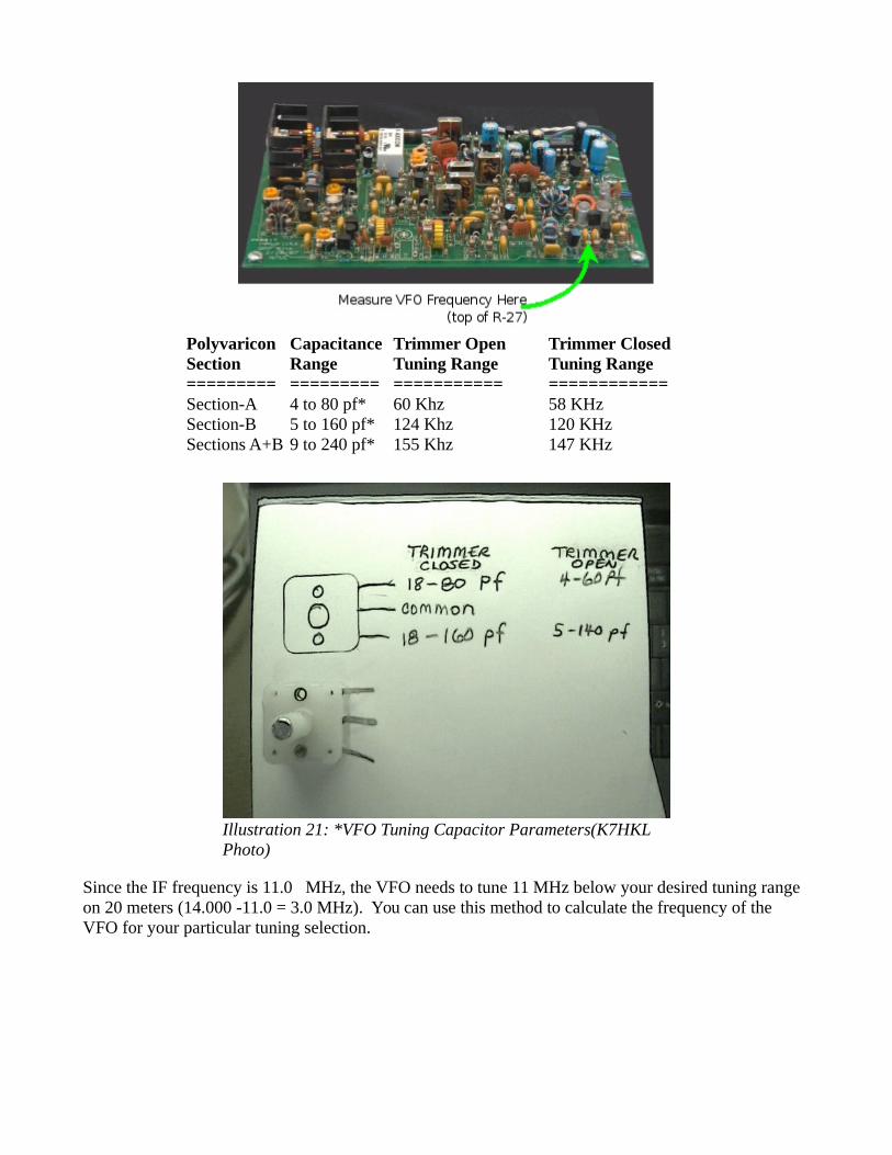
Polyvaricon Capacitance Trimmer Open Trimmer ClosedSection Range Tuning Range Tuning Range========= ========= =========== ============Section-A 4 to 80 pf* 60 Khz 58 KHzSection-B 5 to 160 pf* 124 Khz 120 KHzSections A+B 9 to 240 pf* 155 Khz 147 KHz
Since the IF frequency is 11.0 MHz, the VFO needs to tune 11 MHz below your desired tuning range on 20 meters (14.000 -11.0 = 3.0 MHz). You can use this method to calculate the frequency of the VFO for your particular tuning selection.
Illustration 21: *VFO Tuning Capacitor Parameters(K7HKL Photo)
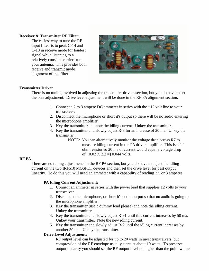
Receiver & Transmitter RF Filter:The easiest way to tune the RF input filter is to peak C-14 and C-18 in receive mode for loudest signal while listening to a relatively constant carrier from your antenna. This provides both receive and transmit mode alignment of this filter.
Transmitter DriverThere is no tuning involved in adjusting the transmitter drivers section, but you do have to set the bias adjustment. Drive level adjustment will be done in the RF PA alignment section.
1. Connect a 2 to 3 ampere DC ammeter in series with the +12 volt line to your transceiver.
2. Disconnect the microphone or short it's output so there will be no audio entering the microphone amplifier.
3. Key the transmitter and note the idling current. Unkey the transmitter.4. Key the transmitter and slowly adjust R-8 for an increase of 20 ma. Unkey the
transmitter.NOTE: You can alternatively monitor the voltage drop across R7 to
measure idling current in the PA driver amplifier. This is a 2.2 ohm resistor so 20 ma of current would equal a voltage drop of (0.02 X 2.2 =) 0.044 volts.
RF PAThere are no tuning adjustments in the RF PA section, but you do have to adjust the idling current on the two IRF510 MOSFET devices and then set the drive level for best output linearity. To do this you will need an ammeter with a capability of reading 2.5 or 3 amperes.
PA Idling Current Adjustment:1. Connect an ammeter in series with the power lead that supplies 12 volts to your
transceiver.2. Disconnect the microphone, or short it's audio output so that no audio is going to
the microphone amplifier.3. Key the transmitter (use a dummy load please) and note the idling current.
Unkey the transmitter.4. Key the transmitter and slowly adjust R-91 until this current increases by 50 ma.
Unkey your transmitter. Note the new idling current.5. Key the transmitter and slowly adjust R-2 until the idling current increases by
another 50 ma. Unkey the transmitter.Drive Level Adjustment:
RF output level can be adjusted for up to 20 watts in most transceivers, but compression of the RF envelope usually starts at about 10 watts. To preserve output linearity you should set the RF output level no higher than the point where

RF compression becomes apparent. As you monitor the RF output and simultaneously increase the drive level, you should see the output rise fairly fast, with the rate of rise decreasing after you pass some point on the adjustment. This is the setting where RF compression starts. For best transmitted signal linearity you should set the drive level just below this start of compression point.
1. You can insert a tone via the microphone jack of your transceiver or use the time-honored method of saying a long � Aaaaaaaaaaaaaah� while monitoring the RF output with a scope, diode detector and voltmeter, or watt meter.
2. Key your transmitter and insert the tone while monitoring the RF output and slowly adjusting the RF drive pot (R-83) for an increase in output. Identify the adjustment position where rate of output increase seems to slow. Back the drive level back down by ½ watt or so. This is your position of best output signal quality. Unkey your transmitter.
NOTE: Do not keep the transmitter keyed for more than a few seconds with a tone input. Steady tones exceed the duty cycle designed into the RF PA amplifiers and their heat sinks, and may overheat the IRF-510 MOSFETS.


![BITX20A Spanish[1]](https://img.pdfslide.net/doc/110x75/5571fd41497959916998b647/bitx20a-spanish1.jpg)