Embed Size (px)
Citation preview
High Boost Hybrid Transformer DC–DC
Converter for Photovoltaic Module Applications
K.Umadevi ,Associate Professor
Abstract—This paper presents a nonisolated, high boost ratio hy-brid transformer dc–dc converter with applications for low-voltage
renewable energy sources. The proposed converter utilizes a hy-brid transformer to transfer the inductive and capacitive energy
simultaneously, achieving a high boost ratio with a smaller sized magnetic component. As a result of incorporating the resonant operation
mode into the traditional high boost ratio pulsewidth modulation converter, the turn-off loss of the switch is reduced, increasing the efficiency
of the converter under all load conditions. The input current ripple and conduction losses are also reduced because of the hybrid linear-
sinusoidal input current waveforms. The voltage stresses on the active switch and diodes are maintained at a low level and are independent of
the changing input voltage over a wide range as a result of the resonant capacitor transfer-ring energy to the output of the converter. The
effectiveness of the proposed converter was experimentally verified using a 220-W prototype circuit. Utilizing an input voltage ranging from
20 to 45 V and a load range of 30–220 W, the experimental results show system of efficiencies greater than 96% with a peak efficiency of
97.4% at 35-V input, 160-W output. Due to the high system effi-ciency and the ability to operate with a wide variable input voltage, the
proposed converter is an attractive design for alternative low dc voltage energy sources, such as solar photovoltaic modules and fuel cells.
Index Terms—energy sources with low dc voltage, European union (EU) effi-ciency, high boost ratio dc–dc, high efficiency, hybrid
transformer, photovoltaic (PV) module.
I. INTRODUCTION
Due to the rising costs and limited amount of nonrenew-able
energy sources, there is an increasing demand for the utilization
of renewable energy sources such as photovoltaic (PV) modules.
Integrating the power from the PV module into the existing power
distribution infrastructure can be achieved through power
conditioning systems (PCS). Typical PCS can be accomplished
using a single-stage or a double-stage as shown in Fig. 1. The
double-stage PCS consists of a dc–dc conversion stage that is
connected to either a low-power individual inverter or a high-
power centralized inverter that multiple converters could connect
to. The dc–dc conversion stage of the PCS requires a high
efficiency, high boost ratio dc– dc converter to increase the low
dc input voltage from the PV panel to a higher dc voltage. This
voltage has to be higher than the peak output voltage of the dc–ac
inverter, nominally in the 380–400 V range. The double-stage
design can also suppress ac line double frequency by utilizing the
active ripple cancellation technique .
The high boost ratio dc–dc converter for such systems can be
isolated or nonisolated however, transformer-isolated converters
tend to be less efficient and more expensive due to the increased
manufacturing costs. A nonisolated dc–dc converter with a high
boost ratio would be advantageous for a two-stage PCS because
it can be easily integrated with current PV systems while reducing
the cost and maintaining a high system efficiency.
Due to the different output voltages from the PV panel, it
would be beneficial to have a system with a high efficiency over
the entire PV voltage range to maximize the use of the PV during
different operating conditions. Another important function of the
DC–DC converter for PV applications is being able to implement
maximum power point tracking (MPPT). The ability to
implement MPPT for an individual PV panel would ensure that a
large cluster of PV could maintain maximum power output from
each panel without interfering with the other panels in the system.
The major consideration for the main power stage of the
converter in being able to implement an accurate MPPT is that
the input current ripple of the converter has to be low.
The high boost ratio nonisolated dc–dc converter the uses of
coupled-inductor and switched-capacitor are attractive for use in a
simple high boost ratio converter due to the fact that only a single
low voltage active switch is required . The reason that the primary
side active switches of the high boost ratio converters have low
voltage stress is because of the transformer effect from the
coupled-inductors .Since there is a low voltage stress on the
active switch, the circuits can then use low voltage MOSFETs
that generally have a low Rds(on) and smaller switching periods,
decreasing both the conduction and switching losses. An earlier
paper on high boost ratio nonisolated dc–dc converter presented a
clamp-mode couple-inductor buck–boost converter. The
converter’s leakage energy from the coupled-inductor was
recycled reducing the losses of the system. The output diode
stress for this converter was similar to that of a traditional
Fig. 1. Typical double-stage PCS architectures with high boost ratio dc–dc converters and PWM dc–ac inverters for PV applications. (a) Two-state PV
module integrated microinverter. (b) Parallal PV module integrated microconverter with centralized inverter
International Journal of Scientific & Engineering Research, Volume 4, Issue 5, May-2013 ISSN 2229-5518
IJSER © 2013 http://www.ijser.org
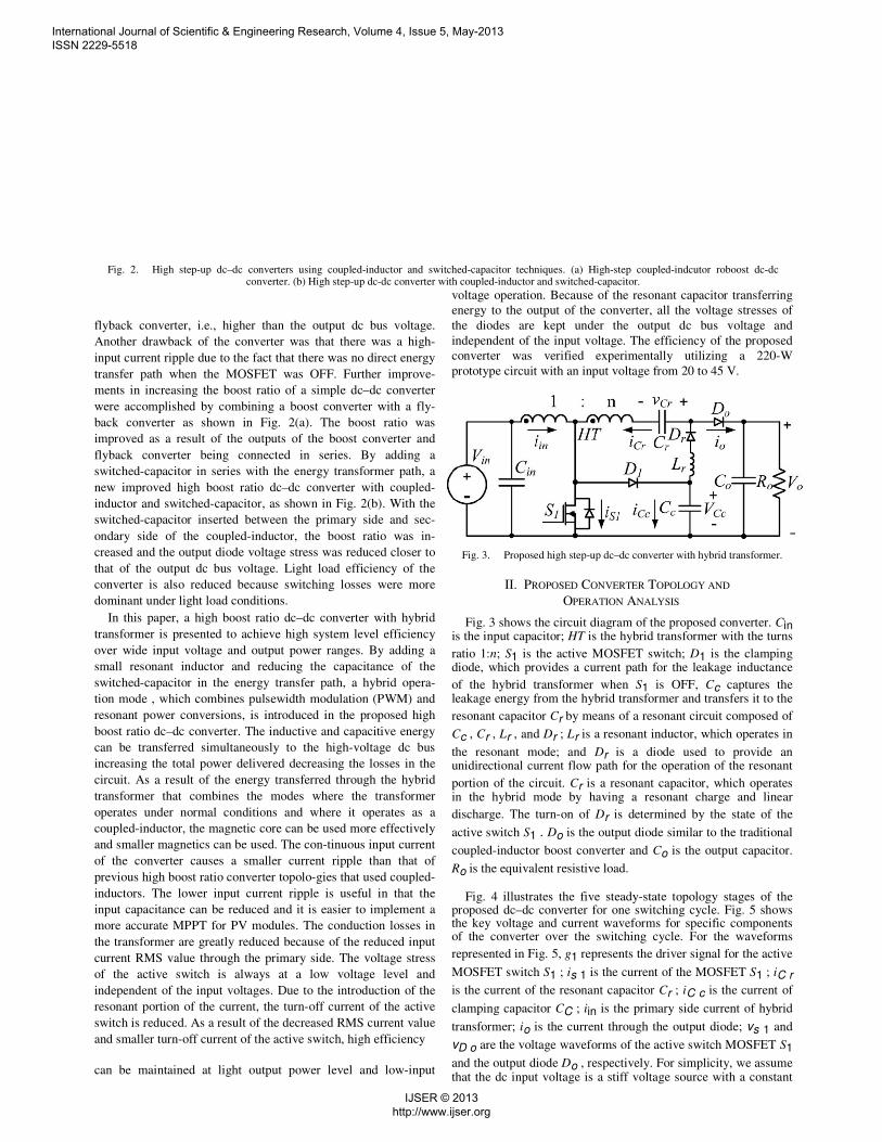
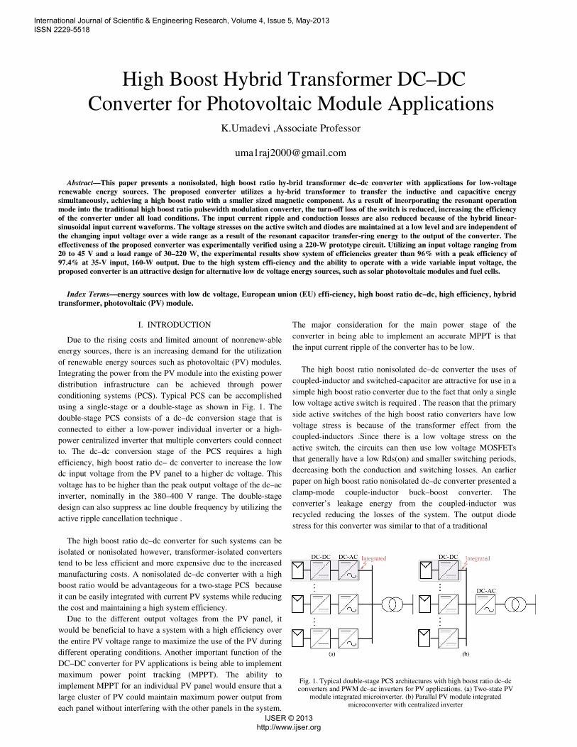
Fig. 2. High step-up dc–dc converters using coupled-inductor and switched-capacitor techniques. (a) High-step coupled-indcutor roboost dc-dc converter. (b) High step-up dc-dc converter with coupled-inductor and switched-capacitor.
flyback converter, i.e., higher than the output dc bus voltage.
Another drawback of the converter was that there was a high-
input current ripple due to the fact that there was no direct energy
transfer path when the MOSFET was OFF. Further improve-
ments in increasing the boost ratio of a simple dc–dc converter
were accomplished by combining a boost converter with a fly-
back converter as shown in Fig. 2(a). The boost ratio was
improved as a result of the outputs of the boost converter and
flyback converter being connected in series. By adding a
switched-capacitor in series with the energy transformer path, a
new improved high boost ratio dc–dc converter with coupled-
inductor and switched-capacitor, as shown in Fig. 2(b). With the
switched-capacitor inserted between the primary side and sec-
ondary side of the coupled-inductor, the boost ratio was in-
creased and the output diode voltage stress was reduced closer to
that of the output dc bus voltage. Light load efficiency of the
converter is also reduced because switching losses were more
dominant under light load conditions. In this paper, a high boost ratio dc–dc converter with hybrid
transformer is presented to achieve high system level efficiency
over wide input voltage and output power ranges. By adding a
small resonant inductor and reducing the capacitance of the
switched-capacitor in the energy transfer path, a hybrid opera-
tion mode , which combines pulsewidth modulation (PWM) and
resonant power conversions, is introduced in the proposed high
boost ratio dc–dc converter. The inductive and capacitive energy
can be transferred simultaneously to the high-voltage dc bus
increasing the total power delivered decreasing the losses in the
circuit. As a result of the energy transferred through the hybrid
transformer that combines the modes where the transformer
operates under normal conditions and where it operates as a
coupled-inductor, the magnetic core can be used more effectively
and smaller magnetics can be used. The con-tinuous input current
of the converter causes a smaller current ripple than that of
previous high boost ratio converter topolo-gies that used coupled-
inductors. The lower input current ripple is useful in that the
input capacitance can be reduced and it is easier to implement a
more accurate MPPT for PV modules. The conduction losses in
the transformer are greatly reduced because of the reduced input
current RMS value through the primary side. The voltage stress
of the active switch is always at a low voltage level and
independent of the input voltages. Due to the introduction of the
resonant portion of the current, the turn-off current of the active
switch is reduced. As a result of the decreased RMS current value
and smaller turn-off current of the active switch, high efficiency
can be maintained at light output power level and low-input
voltage operation. Because of the resonant capacitor transferring
energy to the output of the converter, all the voltage stresses of
the diodes are kept under the output dc bus voltage and
independent of the input voltage. The efficiency of the proposed
converter was verified experimentally utilizing a 220-W
prototype circuit with an input voltage from 20 to 45 V.
Fig. 3. Proposed high step-up dc–dc converter with hybrid transformer.
II. PROPOSED CONVERTER TOPOLOGY AND OPERATION ANALYSIS
Fig. 3 shows the circuit diagram of the proposed converter. Cin is the input capacitor; HT is the hybrid transformer with the turns
ratio 1:n; S1 is the active MOSFET switch; D1 is the clamping diode, which provides a current path for the leakage inductance
of the hybrid transformer when S1 is OFF, Cc captures the leakage energy from the hybrid transformer and transfers it to the
resonant capacitor Cr by means of a resonant circuit composed of
Cc , Cr , Lr , and Dr ; Lr is a resonant inductor, which operates in
the resonant mode; and Dr is a diode used to provide an unidirectional current flow path for the operation of the resonant
portion of the circuit. Cr is a resonant capacitor, which operates in the hybrid mode by having a resonant charge and linear
discharge. The turn-on of Dr is determined by the state of the
active switch S1 . Do is the output diode similar to the traditional
coupled-inductor boost converter and Co is the output capacitor.
Ro is the equivalent resistive load. Fig. 4 illustrates the five steady-state topology stages of the
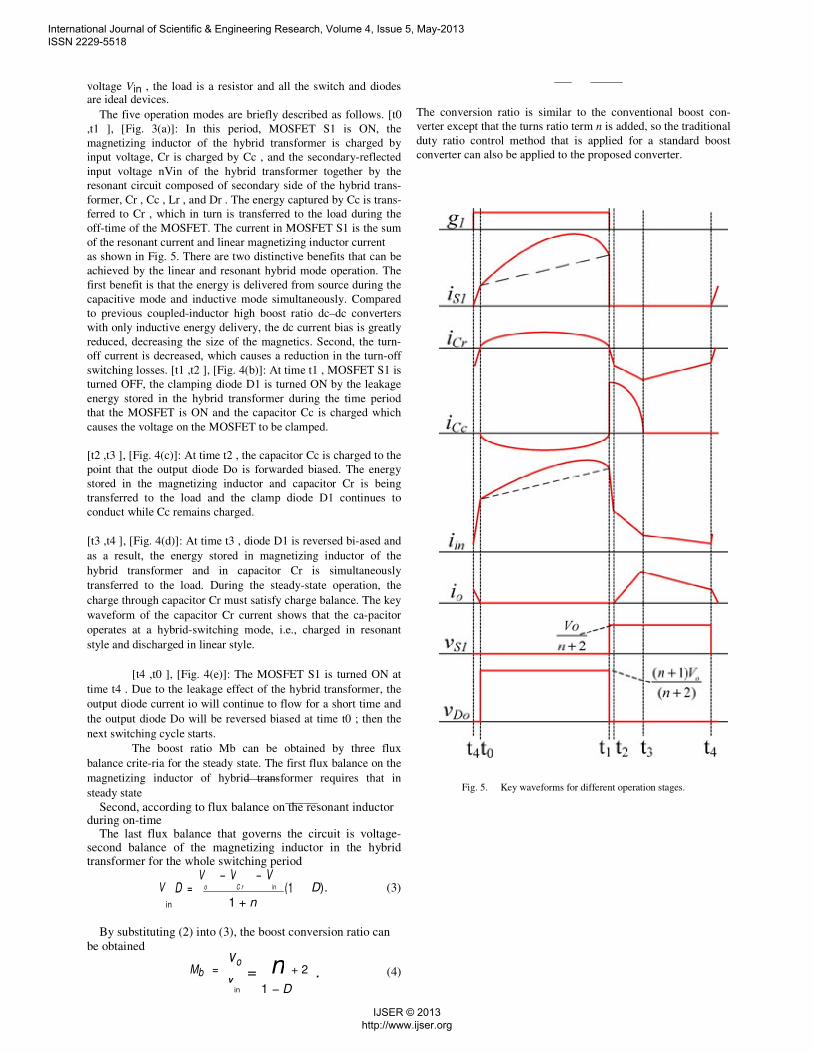
proposed dc–dc converter for one switching cycle. Fig. 5 shows the key voltage and current waveforms for specific components of the converter over the switching cycle. For the waveforms
represented in Fig. 5, g1 represents the driver signal for the active
MOSFET switch S1 ; is 1 is the current of the MOSFET S1 ; iC r
is the current of the resonant capacitor Cr ; iC c is the current of
clamping capacitor CC ; iin is the primary side current of hybrid
transformer; io is the current through the output diode; vs 1 and
vD o are the voltage waveforms of the active switch MOSFET S1
and the output diode Do , respectively. For simplicity, we assume that the dc input voltage is a stiff voltage source with a constant
International Journal of Scientific & Engineering Research, Volume 4, Issue 5, May-2013 ISSN 2229-5518
IJSER © 2013 http://www.ijser.org
voltage Vin , the load is a resistor and all the switch and diodes are ideal devices.
The five operation modes are briefly described as follows. [t0
,t1 ], [Fig. 3(a)]: In this period, MOSFET S1 is ON, the
magnetizing inductor of the hybrid transformer is charged by
input voltage, Cr is charged by Cc , and the secondary-reflected
input voltage nVin of the hybrid transformer together by the
resonant circuit composed of secondary side of the hybrid trans-
former, Cr , Cc , Lr , and Dr . The energy captured by Cc is trans-
ferred to Cr , which in turn is transferred to the load during the
off-time of the MOSFET. The current in MOSFET S1 is the sum
of the resonant current and linear magnetizing inductor current
as shown in Fig. 5. There are two distinctive benefits that can be
achieved by the linear and resonant hybrid mode operation. The
first benefit is that the energy is delivered from source during the
capacitive mode and inductive mode simultaneously. Compared
to previous coupled-inductor high boost ratio dc–dc converters
with only inductive energy delivery, the dc current bias is greatly
reduced, decreasing the size of the magnetics. Second, the turn-
off current is decreased, which causes a reduction in the turn-off
switching losses. [t1 ,t2 ], [Fig. 4(b)]: At time t1 , MOSFET S1 is
turned OFF, the clamping diode D1 is turned ON by the leakage
energy stored in the hybrid transformer during the time period
that the MOSFET is ON and the capacitor Cc is charged which
causes the voltage on the MOSFET to be clamped.
[t2 ,t3 ], [Fig. 4(c)]: At time t2 , the capacitor Cc is charged to the
point that the output diode Do is forwarded biased. The energy
stored in the magnetizing inductor and capacitor Cr is being
transferred to the load and the clamp diode D1 continues to
conduct while Cc remains charged.
[t3 ,t4 ], [Fig. 4(d)]: At time t3 , diode D1 is reversed bi-ased and
as a result, the energy stored in magnetizing inductor of the
hybrid transformer and in capacitor Cr is simultaneously
transferred to the load. During the steady-state operation, the
charge through capacitor Cr must satisfy charge balance. The key
waveform of the capacitor Cr current shows that the ca-pacitor
operates at a hybrid-switching mode, i.e., charged in resonant
style and discharged in linear style.
[t4 ,t0 ], [Fig. 4(e)]: The MOSFET S1 is turned ON at
time t4 . Due to the leakage effect of the hybrid transformer, the
output diode current io will continue to flow for a short time and
the output diode Do will be reversed biased at time t0 ; then the
next switching cycle starts.
The boost ratio Mb can be obtained by three flux
balance crite-ria for the steady state. The first flux balance on the
magnetizing inductor of hybrid transformer requires that in
steady state
Second, according to flux balance on the resonant inductor during on-time
The last flux balance that governs the circuit is voltage-second balance of the magnetizing inductor in the hybrid transformer for the whole switching period
V in
D = V
o − V
C r − V
in (1
D). (3)
1 + n
By substituting (2) into (3), the boost conversion ratio can
be obtained
Mb = Vo
= n + 2 . (4)V
in 1 − D
The conversion ratio is similar to the conventional boost con-
verter except that the turns ratio term n is added, so the traditional
duty ratio control method that is applied for a standard boost
converter can also be applied to the proposed converter.
Fig. 5. Key waveforms for different operation stages.
International Journal of Scientific & Engineering Research, Volume 4, Issue 5, May-2013 ISSN 2229-5518
IJSER © 2013 http://www.ijser.org
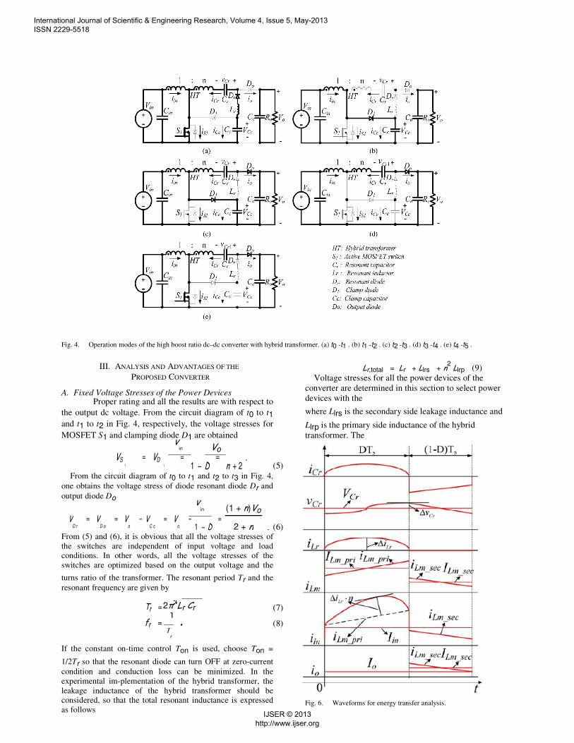
Fig. 4. Operation modes of the high boost ratio dc–dc converter with hybrid transformer. (a) t0 -t1 . (b) t1 -t2 . (c) t2 -t3 . (d) t3 -t4 . (e) t4 -t5 .
III. ANALYSIS AND ADVANTAGES OF THE PROPOSED CONVERTER
A. Fixed Voltage Stresses of the Power Devices
Proper rating and all the results are with respect to
the output dc voltage. From the circuit diagram of t0 to t1
and t1 to t2 in Fig. 4, respectively, the voltage stresses for
MOSFET S1 and clamping diode D1 are obtained V
in Vo
VS 1 = VD 1 = 1 − D
= n + 2 . (5)
From the circuit diagram of t0 to t1 and t2 to t3 in Fig. 4,
one obtains the voltage stress of diode resonant diode Dr and
output diode Do V
in (1 + n)Vo
VD r = VD o = Vo − VC c = Vo − 1 − D
=
. (6)
2 + n
From (5) and (6), it is obvious that all the voltage stresses of
the switches are independent of input voltage and load conditions. In other words, all the voltage stresses of the
switches are optimized based on the output voltage and the
turns ratio of the transformer. The resonant period Tr and the
resonant frequency are given by
Tr =2π₃Lr Cr (7)
fr =1 . (8)
T
r
If the constant on-time control Ton is used, choose Ton =
1/2Tr so that the resonant diode can turn OFF at zero-current
condition and conduction loss can be minimized. In the
experimental im-plementation of the hybrid transformer, the
leakage inductance of the hybrid transformer should be considered, so that the total resonant inductance is expressed
as follows
Lr,total = Lr + Llrs + n2 Llrp (9)
Voltage stresses for all the power devices of the
converter are determined in this section to select power
devices with the
where Llrs is the secondary side leakage inductance and
Llrp is the primary side inductance of the hybrid
transformer. The
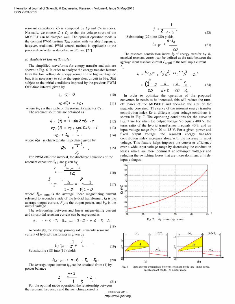
Fig. 6. Waveforms for energy transfer analysis.
International Journal of Scientific & Engineering Research, Volume 4, Issue 5, May-2013 ISSN 2229-5518
IJSER © 2013 http://www.ijser.org
resonant capacitance Cr is composed by Cr and Cc in series.
Normally, we choose Cr ₃ Cc so that the voltage stress of the
MOSFET can be clamped well. The optimal operation mode is
the constant PWM on-time Ton control with variable frequency,
however, traditional PWM control method is applicable to the
proposed converter as described in [26] and [27].
B. Analysis of Energy Transfer
The simplified waveforms for energy transfer analysis are
shown in Fig. 6. In order to analyze the energy transfer feature
from the low voltage dc energy source to the high-voltage dc
bus, it is necessary to solve the equivalent circuit in Fig. 3(a)
subject to the initial conditions imposed by the previous PWM
OFF-time interval given by
iL r (0)= 0 (10)
vC r (0)= − vC r (11)
where vC r is the ripple of the resonant capacitor Cr . The resonant solutions are obtained as
iL r (t) =i
L r sin 2πfr · t (12)
vC r (t) = vC r cos 2πfr · t (13)
vC r = RN · iL r (14)
where RN is characteristic impedance given by
RN = ₃ Lr . (15)
Cr For PWM off-time interval, the discharge equations of the
resonant capacitor Cr 1 are given by
vC r =
ILm sec Toff
(16)
2Cr
I
Lm sec = Io = P
o 1 (17)
1 − D 1 − D
Vo
where ILm sec is the average linear magnetizing current
referred to secondary side of the hybrid transformer, Io is the
average output current, Po is the output power, and Vo is the output voltage.
The relationship between and linear magne-tizing current
and sinusoidal resonant current can be expressed as
iL r = π · fr · Ts · ILm sec · (1 − D) = π · fr · Ts · Io .
(18) Accordingly, the average primary side sinusoidal resonant
current of hybrid transformer is given by
LLr pri = π1 n ·
iL r . (19)
Substituting (18) into (19) yields
LLr pri = n · fr · Ts · Io . (20) The average input current Iin can be obtained from (4) by
power balance n + 2
Iin = 1 − D
· Io . (21)For the optimal mode operation, the relationship between
the resonant frequency and the switching period is
1
fr = 2 · D · Ts . (22)
Substituting (22) into (20) yields
LLr pri = n · Io
. (23)
2D
The resonant contribution index kr of energy transfer by si-nusoidal resonant current can be defined as the ratio between the
average input resonant current LLr pri to the total input current I
in
kr = LLr
I pri =
n2
·DI
o ₃ ₃ 1n +D2 · Io ₃
in −
= (1 − D) n = n V
in . (24)
·
2D ·
2D n + 2 Vo
In order to optimize the operation of the proposed
converter, kr needs to be increased, this will reduce the turn-
off losses of the MOSFET and decrease the size of the
magnetic core used. The curve of the resonant energy transfer
contribution index Kr at different input voltage conditions is
shown in Fig. 7. The oper-ating conditions for the curve in
Fig. 7 are for when the output voltage Vo equals 400 V, the
turns ratio of the hybrid transformer n equals 40:9, and an
input voltage range from 20 to 45 V. For a given power and
fixed output voltage, the resonant energy trans-fer
contribution index increases along with the increase in input
voltage. This feature helps improve the converter efficiency
over a wide input voltage range by decreasing the conduction
losses which are more dominant at low-input voltages and
reducing the switching losses that are more dominant at high-
input voltages.
Fig. 7. Kr versus Vin curve.
Fig. 8. Input current comparison between resonant mode and linear mode.
(a) Resonant mode. (b) Linear mode.
International Journal of Scientific & Engineering Research, Volume 4, Issue 5, May-2013 ISSN 2229-5518
IJSER © 2013 http://www.ijser.org
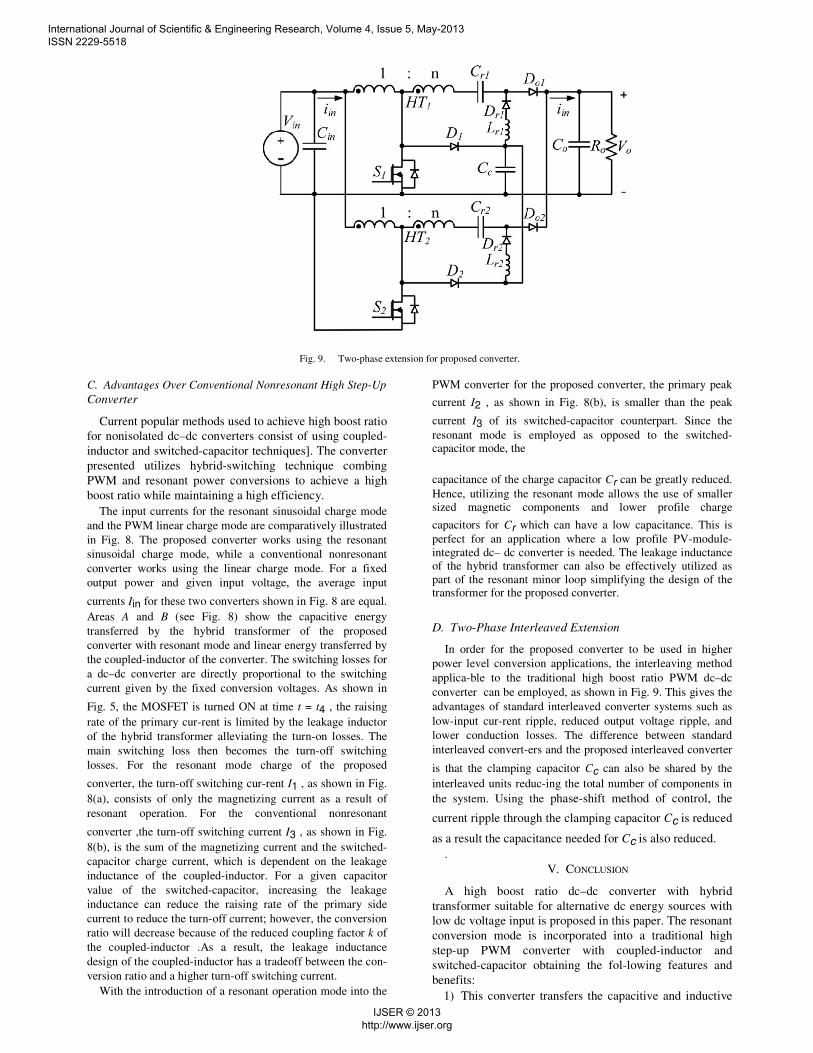
Fig. 9. Two-phase extension for proposed converter.
C. Advantages Over Conventional Nonresonant High Step-Up Converter
Current popular methods used to achieve high boost ratio
for nonisolated dc–dc converters consist of using coupled-
inductor and switched-capacitor techniques]. The converter
presented utilizes hybrid-switching technique combing
PWM and resonant power conversions to achieve a high
boost ratio while maintaining a high efficiency. The input currents for the resonant sinusoidal charge mode
and the PWM linear charge mode are comparatively illustrated
in Fig. 8. The proposed converter works using the resonant
sinusoidal charge mode, while a conventional nonresonant
converter works using the linear charge mode. For a fixed
output power and given input voltage, the average input
currents Iin for these two converters shown in Fig. 8 are equal.
Areas A and B (see Fig. 8) show the capacitive energy
transferred by the hybrid transformer of the proposed
converter with resonant mode and linear energy transferred by
the coupled-inductor of the converter. The switching losses for
a dc–dc converter are directly proportional to the switching
current given by the fixed conversion voltages. As shown in
Fig. 5, the MOSFET is turned ON at time t = t4 , the raising
rate of the primary cur-rent is limited by the leakage inductor
of the hybrid transformer alleviating the turn-on losses. The
main switching loss then becomes the turn-off switching
losses. For the resonant mode charge of the proposed
converter, the turn-off switching cur-rent I1 , as shown in Fig.
8(a), consists of only the magnetizing current as a result of
resonant operation. For the conventional nonresonant
converter ,the turn-off switching current I3 , as shown in Fig.
8(b), is the sum of the magnetizing current and the switched-
capacitor charge current, which is dependent on the leakage
inductance of the coupled-inductor. For a given capacitor
value of the switched-capacitor, increasing the leakage
inductance can reduce the raising rate of the primary side
current to reduce the turn-off current; however, the conversion
ratio will decrease because of the reduced coupling factor k of
the coupled-inductor .As a result, the leakage inductance
design of the coupled-inductor has a tradeoff between the con-
version ratio and a higher turn-off switching current. With the introduction of a resonant operation mode into the
PWM converter for the proposed converter, the primary peak
current I2 , as shown in Fig. 8(b), is smaller than the peak
current I3 of its switched-capacitor counterpart. Since the
resonant mode is employed as opposed to the switched-capacitor mode, the
capacitance of the charge capacitor Cr can be greatly reduced.
Hence, utilizing the resonant mode allows the use of smaller sized magnetic components and lower profile charge
capacitors for Cr which can have a low capacitance. This is
perfect for an application where a low profile PV-module-
integrated dc– dc converter is needed. The leakage inductance of the hybrid transformer can also be effectively utilized as
part of the resonant minor loop simplifying the design of the transformer for the proposed converter.
D. Two-Phase Interleaved Extension
In order for the proposed converter to be used in higher
power level conversion applications, the interleaving method
applica-ble to the traditional high boost ratio PWM dc–dc
converter can be employed, as shown in Fig. 9. This gives the
advantages of standard interleaved converter systems such as
low-input cur-rent ripple, reduced output voltage ripple, and
lower conduction losses. The difference between standard
interleaved convert-ers and the proposed interleaved converter
is that the clamping capacitor Cc can also be shared by the
interleaved units reduc-ing the total number of components in
the system. Using the phase-shift method of control, the
current ripple through the clamping capacitor Cc is reduced
as a result the capacitance needed for Cc is also reduced. .
V. CONCLUSION
A high boost ratio dc–dc converter with hybrid
transformer suitable for alternative dc energy sources with
low dc voltage input is proposed in this paper. The resonant
conversion mode is incorporated into a traditional high
step-up PWM converter with coupled-inductor and
switched-capacitor obtaining the fol-lowing features and
benefits: 1) This converter transfers the capacitive and inductive
International Journal of Scientific & Engineering Research, Volume 4, Issue 5, May-2013 ISSN 2229-5518
IJSER © 2013 http://www.ijser.org
en-ergy simultaneously to increase the total power
delivery reducing losses in the system. 2) The conduction loss in the transformer and MOSFET
is re-duced as a result of the low-input RMS current and switch-ing loss is reduced with a lower turn-off current. With these improved performances, the converter can maintain high efficiency under low output power and low-input voltage conditions.
3) With low-input ripple current feature, the converter is
suit-able for PV module and fuel cell PCS, where, accurate
MPPT is performed by the dc–dc converter. A prototype-circuit-targeted PV module power optimizer
with 20–45 V input voltage range and 400-V dc output was
built and tested. Experimental results show that the
MOSFET voltage was clamped at 60 V and the output
diode voltage was under 350 V. These results were
independent of the input voltage level. The conversion
efficiencies from 30 to 220 W are higher than 96% and the
peak efficiency is 97.4% under 35-V input with 160-W
output power.
REFERENCES
[1] J.-S. Lai, “Power conditioning circuit topologies,” IEEE Ind.
Electron. Mag., vol. 3, no. 2, pp. 24–34, Jun. 2009. [2] S. B. Kjaer, J. K. Pedersen, and F. Blaabjerg, “A review of single-
phase grid-connected inverters for photovoltaic modules,” IEEE Trans. Ind. Appl., vol. 41, no. 5, pp. 1292–1306, Sep./Oct. 2005.
[3] F. Blaabjerg, Z. Chen, and S. B. Kjaer, “Power electronics as efficient interface in dispersed power generation systems,” IEEE Trans. Power Electron., vol. 19, no. 5, pp. 1184–1194, Sep. 2004.
International Journal of Scientific & Engineering Research, Volume 4, Issue 5, May-2013 ISSN 2229-5518
IJSER © 2013 http://www.ijser.org