Embed Size (px)
Citation preview

High Efficiency DC-DC Converter for EV
Battery Charger Using Hybrid Resonant and
PWM Technique
Hongmei Wan
Thesis submitted to the faculty of the
Virginia Polytechnic Institute and State University
in partial fulfillment of the requirements for the degree of
Master of Science
In
Electrical and Computer Engineering
Jih-Sheng Lai, Chair
Douglas J. Nelson
Kathleen Meehan
April 30, 2012
Blacksburg, Virginia
Keywords: Electric Vehicle Battery Charger, DC-DC Converter, Phase-shifted Full
Bridge Converter, LLC Resonant Converter, Hybrid Resonant and PWM Converter
Copyright 2012, Hongmei Wan

High Efficiency DC-DC Converter for EV
Battery Charger Using Hybrid Resonant and
PWM Technique
Hongmei Wan
ABSTRACT
The battery charger plays an important role in the development of electric vehicles
(EVs) and plug-in hybrid electric vehicles (PHEVs).This thesis focuses on the DC-DC
converter for high voltage battery charger and is divided into four chapters. The
background related to EV battery charger is introduced, and the topologies of isolated DC-
DC converter possibly applied in battery charge are sketched in Chapter 1. Since the EV
battery charger is high voltage high power, the phase-shifted full bridge and LLC
converters, which are popularly used in high power applications, are discussed in detail in
Chapter 2. They are generally considered as high efficiency, high power density and high
reliability, but their prominent features are also limited in certain range of operation. To
make full use of the advantages and to avoid the limitation of the phase-shifted full bridge
and LLC converters, a novel hybrid resonant and PWM converter combining resonant
LLC half-bridge and phase shifted full-bridge topology is proposed and is described in
Chapter 3. The converter achieves high efficiency and true soft switching for the entire
operation range, which is very important for high voltage EV battery charger application.
A 3.4 kW hardware prototype has been designed, implemented and tested to verify that
the proposed hybrid converter truly avoids the disadvantages of LLC and phase-shifted
full bridge converters while maintaining their advantages. In this proposed hybrid
converter, the utilization efficiency of the auxiliary transformer is not that ideal. When the
duty cycle is large, LLC converter charges one of the capacitors but the energy stored in
the capacitor has no chance to be transferred to the output, resulting in the low utilization

iii
efficiency of the auxiliary transformer. To utilize the auxiliary transformer fully while
keeping all the prominent features of the previous hybrid converter in Chapter 3, an
improved hybrid resonant and PWM converter is proposed in Chapter 4. The idea has
been verified with simulations. The last chapter is the conclusion which summaries the
key features and findings of the two proposed hybrid converters.

iv
ACKNOWLEDGEMENTS
First, I would like to express my deep gratitude and appreciation to my advisor, Dr.
Jih-Sheng Lai. His knowledge, research attitude and ways of thinking are most valuable
during my years of study and they will keep helping me in my future life. His guidance,
expertise, patience, and encouragement were essential during my time at Virginia Tech.
The lessons I learned from him will guide me throughout my life.
I am grateful to my committee: Dr. Kathleen Meehan and Dr. Douglas J. Nelson for
their guidance and for serving on my committee. Both Dr. Kathleen Meehan and Dr.
Douglas J. Nelson help make Virginia Tech’s Bradley Department of Electrical and
Computer Engineering into the excellent program that it is.
The classes I took at Virginia Tech provided me with knowledge critical for my
graduate work. I would like to thank the Virginia Tech professors who taught the classes
for sharing their valuable experience and knowledge.
I would also like to extend my thanks to my colleagues in the Future Energy
Electronics Center (FEEC). Mr. Gary Kerr, Mr, Dr. Wensong Yu, Mr. Wei-Han Lai, Mr.
Hidekazu Miwa, Mr.YoungHoon Cho, Mr. Pengwei Sun, Mr. Jian-Liang Chen,
Mr.ThomasLaBella, Mr. Christopher Hutchens, Mr. Benjamin York, Mr. Bret Whitaker,
Mr. Hao Qian, Mr. Zidong Liu, Mr. Hsin Wang, Mr. Ahmed Koran, Mr. Cong Zheng,
Mr. Baifeng Chen, Mr. Rui Chen, ZakariyaDalala, Mr. Bin Gu , Seung-Ryul Moon ,
Yaxiao Qin, Ms.Zheng Zhao , Mr. ZakaUllahZahid ,Ms. Hyun SooKoh , and
Mr.JohnReichl, all assisted me greatly. In addition, I would like to extend my gratitude to
visiting scholars, Prof. Huang-Jen Chiu, Prof. Yen-Shin Lai, Mr. Hongbo Ma, and
Mr.Chuang Liu.
My greatest gratitude and thanks go to my family. My husband, Wensong Yu,
provides me countless amounts of support and my son, Yunlong Yu, gives me a lot of fun
and happiness. I would like to thank my father, Wenbiao Wan, mother, ChadeXiong,
brothers, Yinhua Wan and Yaohua Wan, sisters, Yinmei Wan and Xiaomei Wan, for their
encouragement and support in my life.
All photographs by author, 2012.

v
TABLE OF CONTENTS
CH1: Introduction ............................................................................................................ 1 1.1 Background .................................................................................................................................... 1
1.1.1 Typical Battery Charging Profile ............................................................................................ 2
1.1.2 Charger Classifications ........................................................................................................... 4
1.2 Charger System .............................................................................................................................. 6
1.3 Charger System Requirements for Isolated DC-DC Converters .................................................... 7
1.4 Conventional Isolated DC-DC Converters .................................................................................... 8
1.4.1 Basic Isolated PWM Converters ............................................................................................. 8
1.4.2 Basic Resonant Converters .................................................................................................... 11
1.5 Topology Selection for EV Battery Charger ................................................................................ 16
1.6 Thesis Outline .............................................................................................................................. 17
CH2: Phase-Shifted Full Bridge and LLC Resonant Converters for High Power
Application....................................................................................................................... 18 2.1 Introduction.................................................................................................................................. 18
2.2 Phase Shifted Full Bridge Converter ........................................................................................... 20
2.2.1 Topology Description ............................................................................................................ 20
2.2.2 Operating Modes ................................................................................................................... 22
2.2.3 ZVS Process .......................................................................................................................... 26
2.2.4 Relation between Duty Cycle, Transformer Turns Ratio and Switching Frequency ............. 29
2.2.5 Disadvantages of Phase-shifted Full Bridge Converter ......................................................... 30
2.3 LLC Resonant Converter ............................................................................................................. 32
2.3.1 Switching Frequency Equal to Resonant Frequency ............................................................. 36
2.3.2 Switching Frequency Lower Than Resonant Frequency ....................................................... 38
2.3.3 Switching Frequency Higher Than Resonant Frequency ...................................................... 39
2.3.4 Design Considerations of LLC Resonant Converter ............................................................. 41
2.3.5 Disadvantages of LLC Resonant Converter .......................................................................... 44
CH3: Hybrid Resonant and PWM Converter .............................................................. 46 3.1 Motivations .................................................................................................................................. 46
3.2 Proposed Hybrid Resonant and PWM Converter ........................................................................ 46
3.3 Operational Principles .................................................................................................................. 47
3.4 Design Considerations ................................................................................................................. 53
3.4.1 Transformers Turns Ratio ..................................................................................................... 53
3.4.2 ZVS under True Zero Load condition ................................................................................... 54

vi
3.4.4 Duty Cycle Loss .................................................................................................................... 55
3.4.5 Transformer Magnetizing and Leakage inductance .............................................................. 56
3.4.6 Resonant Capacitance ........................................................................................................... 59
3.4.7 Output Inductance ................................................................................................................. 60
3.5 Simulation Circuit and Simulation Results .................................................................................. 61
3.6 Performance Analysis of Hybrid Resonant and PWM Converter ................................................ 64
3.6.1 Main Components in This Circuit ......................................................................................... 66
3.6.2 MOSFETs and IGBTs Conduction Loss Analysis ................................................................ 66
3.6.3 Diode Conduction Loss Analysis .......................................................................................... 70
3.6.4 MOSFET and IGBT Switching Loss Analysis...................................................................... 70
3.6.5 Transformer Core Loss Analysis ........................................................................................... 73
3.6.6 Transformer Copper Loss Analysis ....................................................................................... 76
3.6.7 Inductor Loss ......................................................................................................................... 77
3.6.8 Other Losses .......................................................................................................................... 79
3.6.9 Efficiency Estimation ............................................................................................................ 80
3.7 Topology Variations .................................................................................................................... 81
3.8 Implemented Hardware ................................................................................................................ 83
3.8.1 Complete Circuit Structure .................................................................................................... 83
3.8.2 Implemented Hardware Prototype ......................................................................................... 83
3.8.3 Experimental Verification ..................................................................................................... 83
3.9 Summary ..................................................................................................................................... 86
CH4: Improved Hybrid Resonant and PWM Converter ............................................ 89 4.1 Issues in Previous Hybrid Resonant and PWM Converter .......................................................... 89
4.2 The Improved Hybrid Resonant and PWM Converter................................................................. 90
4.2.1 Operational Principles ........................................................................................................... 90
4.2.2 Design Considerations ................................................................................................. 96
4.3 Simulation Verification ...............................................................................................................100
4.4 Comparisons between the Proposed and Improved Converters ..................................................103
4.5 Summary .....................................................................................................................................106
Conclusion ..................................................................................................................... 108
References ...................................................................................................................... 110

vii
LIST OF FIGURES
Fig.1.1 Electric vehicle and its main modules ....................................................................................... 1 Fig.1.2 System architecture of HEV/EV ............................................................................................... 2 Fig.1.3 Typical charging profile of Li-Ion cell ...................................................................................... 3 Fig.1.4 Block diagram of off-board charger .......................................................................................... 4 Fig.1.5 Block diagram of on-board charger ........................................................................................... 5 Fig.1.6 Battery charger system ............................................................................................................ 6 Fig.1.7 Half bridge SRC ................................................................................................................... 12 Fig.1.8 Half Bridge PRC ................................................................................................................... 13 Fig.1.9 Half Bridge SPRC ................................................................................................................. 14 Fig.1.10 Half Bridge LLC Resonant Converter ................................................................................... 15 Fig.2.1 Phase-shifted Full bridge converter ......................................................................................... 20 Fig.2.2 The difference between regular Full Bridge and PH-Full Bridge ZVS PWM DC/DC converter topologies control switching .............................................................................................................. 21 Fig.2.3 Phase-shifted Full bridge converter ........................................................................................ 22 Fig.2.4 Mode1: at time t1 .................................................................................................................. 23 Fig.2.5 Mode2: at interval t1~t2 .......................................................................................................... 23 Fig.2.6 Mode3: at interval t2~t3 ........................................................................................................ 24 Fig.2.7 Mode4: at interval t3~t4 .......................................................................................................... 24 Fig.2.8 Mode5: at time t4................................................................................................................... 25 Fig.2.9 Mode6: interval t4~t5 ............................................................................................................. 25 Fig.2.10 Detail of the rising edge of the voltage across the switch of lagging leg ................................... 26 Fig.2.11 Detail of the rising edge of the voltage across the switch of leading leg .................................... 28 Fig.2.12 Relation between duty cycle, transformer turns ratio and switching frequency .......................... 30 Fig.2.13 Key waveforms and formula of conventional PSFB converter ................................................. 30 Fig.2.14 Half Bridge LLC Resonant Converter ................................................................................... 32 Fig.2.15 Equivalent Circuit for Half Bridge LLC Resonant Converter................................................... 33 Fig.2.16 LLC Equivalent Circuit ....................................................................................................... 33 Fig.2.17 Gain curves of half bridge LLC ............................................................................................ 34 Fig.2.18 Operating Regions for LLC Resonant Converter .................................................................... 35 Fig.2.19 DC Characteristic of LLC Resonant Converter ...................................................................... 35 Fig.2.20 The switching frequency vs. the peak gain frequency ............................................................. 36 Fig.2.21 LLC converter operating at resonant frequency ..................................................................... 37 Fig.2.22 LLC converter operating at lower resonant frequency ............................................................ 38 Fig.2.23 Topological modes for LLC converter operating at lower resonant frequency .......................... 39 Fig.2.24 LLC converter operating at higher resonant frequency ........................................................... 39 Fig.2.25 Topological modes for LLC converter operating at higher resonant frequency ......................... 40 Fig.2.26 Dead-time requirement ....................................................................................................... 42 Fig.2.27 Peak Gain vs Q for different m values .................................................................................. 43 Fig.2.28 Determining the Maximum Gain .......................................................................................... 44 Fig.2.29 Key characteristics and formula of HB LLC converter ............................................................ 45 Fig. 3.1 Hybrid Resonant and PWM Converter ................................................................................... 47 Fig. 3.2 Hybrid Resonant and PWM Converter ................................................................................... 48 Fig. 3.3 Topological modes of the proposed converter in half switching cycle ....................................... 48 Fig.3.4 (a), (b) The equivalent circuit for Mode [t0, t1]; (c) the key waveforms ....................................... 49 Fig.3.5 The simplified circuit for the primary side of Fig.3.4 (b) ........................................................... 50 Fig.3. 6 The simplified circuit for the secondary side of Fig.3.5 (b) ...................................................... 50 Fig.3.7 The equivalent circuit under zero load condition (worst case) ................................................... 51 Fig.3.8 (a), (b)The equivalent circuit for Mode [t2, t3];(c) zoomed key waveforms ................................ 52 Fig.3.9 (a), (b) the equivalent circuit for Mode [t5, t6]; (c) zoomed key waveforms ................................. 53 Fig.3. 10 The secondary rectifier voltage waveform ............................................................................ 54 Fig.3.11 Voltage gain vs. effective duty cycle ..................................................................................... 54

viii
Fig. 3.12 ZVS condition under no load ............................................................................................... 55 Fig. 3.13 Waveforms of rectified voltage vrect, main transformer TR1 primary voltage vpri1 and main transformer TR1 primary current ipri1 .................................................................................................. 56 Fig. 3.14 Alternative transformer winding configurations .................................................................... 57 Fig.3.15 DC characteristics of half bridge LLC ................................................................................... 58 Fig.3.16 LLC converter voltage gain vs. normalized frequency ............................................................ 59 Fig. 3.17 Voltage waveforms of rectifier ............................................................................................ 60 Fig.3.18 Normalized peak-to-peak output inductor current vs. normalized output voltage. ...................... 60 Fig.3.19 Power stage of the simulation circuit ..................................................................................... 61 Fig.3.20 IGBT waveforms of the voltage, current, and its gate at full load ............................................. 62 Fig.3.21 MOSFET waveforms of the voltage, current, gate and output current at full load ...................... 62 Fig.3.22 MOSFET waveforms of the voltage, current, gate and output current at no load ....................... 63 Fig. 3.23 Full-bridge diode D1 waveforms of voltage, current and its associated transformer secondary current at full load ............................................................................................................................ 63 Fig. 3.24 Half-bridge diode D5 waveforms of voltage and its associated transformer secondary current at full load ........................................................................................................................................... 64 Fig. 3.25 Reading data from data sheet ............................................................................................... 67 Fig.3.26 Reading RDS(on)max (25°C) from the data-sheet ........................................................................ 68 Fig. 3.27 Diode resistance vs. the diode current .................................................................................. 68 Fig. 3.28 Reading data from datasheet ................................................................................................ 69 Fig. 3.29 Definitions of MOSFET switching times and energies ........................................................... 71 Fig. 3.30 Definitions of IGBT switching times and energies ................................................................. 72 Fig.3.31 An arbitrary voltage waveforms ............................................................................................ 73 Fig. 3.32 Core loss density curves of the output inductor ..................................................................... 78 Fig.3.33 Calculated total loss and efficiency vs. output power .............................................................. 81 Fig. 3.34 Estimated power losses at 3.4 kW rated output power with two different output voltage levels.. 81 Fig.3.35 Several variations hybrid resonant and PWM converters ......................................................... 82 Fig.3.36 Complete structure of the implemented hardware ................................................................... 83 Fig.3.37 Prototype of the implemented hardware ................................................................................ 83 Fig. 3.38 Power circuit and the parameters of the prototype ................................................................. 84 Fig.3.39 IGBT ZCS experiment waveforms of device voltage, current, and its gate ............................... 84 Fig. 3.40 MOSFET ZVS load adaptability experiments with different load conditions ........................... 85 Fig.3.41 Full-bridge diode D1 waveforms of voltage, current and its associated transformer secondary current. ............................................................................................................................................ 85 Fig. 3.42 Half-bridge diode D5 experimental waveforms of voltage and its associated transformer secondary current. ............................................................................................................................ 86 Fig. 3.43 Experimental results of efficiency as a function of the output power. ...................................... 86 Fig.3.44 Key waveforms and formulaof the proposed hybrid converter ................................................. 87 Fig. 4.1 Hybrid resonant and PWM converter in CH3 .......................................................................... 89 Fig. 4.2 Mode [t0, t1] for the hybrid resonant and PWM converter ....................................................... 89 Fig. 4.3 The improved circuit configuration ........................................................................................ 90 Fig. 4.4 The improved converter ........................................................................................................ 91 Fig. 4.5 Topological modes of the improved converter in half switching cycle....................................... 91 Fig.4.6 (a), (b) The equivalent circuit for Mode [t0, t1];(c) The key waveforms ...................................... 92 Fig.4.7 The simplified circuit for the primary side of Fig.4.6 (b) ........................................................... 93 Fig.4.8 The simplified circuit for the secondary side of Fig.4.6 (b) ....................................................... 93 Fig.4.9 The equivalent circuit under zero load condition (worst case) ................................................... 94 Fig.4.10 (a), (b) the equivalent circuit for Mode [t2, t3]; (c) the key zoomed waveforms .......................... 95 Fig.4.11 (a), (b) the equivalent circuit for Mode [t5, t6];(c)the key zoomed waveforms ........................... 96 Fig.4.12 The secondary rectifier voltage waveform ............................................................................. 97 Fig.4.13 Voltage gain vs. effective duty cycle ..................................................................................... 97 Fig. 4.14 Waveforms of rectified voltage vrect, main transformer TR1 primary voltage vpri1 and main transformer TR1 primary current ipri1 .................................................................................................. 98 Fig. 4.15 Voltage waveforms of rectifier ............................................................................................ 98 Fig. 4.16 Normalized peak-to-peak output inductor current vs. normalized output voltage. ..................... 99 Fig.4.17 Power stage of the simulation circuit ................................................................................... 100

ix
Fig.4.18 IGBT waveforms of the voltage, current, and its gate at full load ........................................... 101 Fig.4.19 MOSFET waveforms of the voltage, current, gate and output current at full load .................... 101 Fig.4.20 MOSFET waveforms of the voltage, current, gate and output current at no load ..................... 102 Fig. 4.21 Full-bridge diode D1 waveforms of voltage, current and its associated transformer secondary current at full load .......................................................................................................................... 102 Fig. 4.22 Half-bridge diode D5 waveforms of voltage and its associated transformer secondary current at full load ......................................................................................................................................... 103 Fig. 4.23 Circuit configurations of the two converters ........................................................................ 104 Fig.4.24 The secondary rectifier voltage waveform .......................................................................... 105 Fig. 4.25 Normalized peak-to-peak output inductor current vs. normalized output voltage ................... 105

x
LIST OF TABLES
Table1.1: Battery charger classification ................................................................................................ 4 Table 1.2: Battery charging levels ........................................................................................................ 6 Table 1.3: Power Supply Topologies from www.ti.com ....................................................................... 10 Table 3.1: Simulation specifications ................................................................................................... 61 Table 3.2: main components used in the circuit ................................................................................... 66 Table 3.3: factors applied to the above formula (3.49) ......................................................................... 75 Table 3.4: Efficiency estimation conditions ........................................................................................ 80 Table 3.5: phase-shifted full bridge, LLC and Proposed Converters ...................................................... 87 Table 4.1: Simulation specifications ................................................................................................. 100 Table 4.2: Phase-shifted full bridge, LLC, Previous Proposed and Improved Converters ...................... 106

1
CH1: Introduction
1.1 Background
As generally recognized, electric vehicles can achieve higher energy conversion
efficiency, motor-regenerative braking capability, fewer local exhaust emissions, and less
acoustic noise and vibration, as compared to gas-engine vehicles. The battery has an
important role in the development of electric vehicles (EVs) and plug-in hybrid electric
vehicles (PHEVs).
Fig.1.1 Electric vehicle and its main modules
An EV shown in Fig.1.1 [1] is a vehicle propelled by electricity, unlike the
conventional vehicles on road today which are major consumers of fossil fuels. This
electricity can be either produced outside the vehicle and stored in a battery or produced
on board with the help of fuel cells (FC’s). The development of EV’s started as early as
1834 when the first battery powered EV (tricycle) was built by Thomas Davenport [2],
which appeared to be appalling, as it even preceded the invention of the ICE based on
gasoline or diesel fuel. The development of EV’s was discontinued as they were not very
convenient and efficient to use as they were very heavy and took a long time to recharge.
Moreover, from the end of the year 1910, they also became more expensive than ICE

2
vehicles. This led to the development of gasoline based vehicles. However, there are
concerns over the depletion of fossil fuel and green house gases causing long term global
crisis like climatic changes and global warming. These concerns are shifting the focus
back to development of automotive vehicles which use alternative fuels for operations.
The development of such vehicles has become imperative not only for the scientists but
also for the governments around the globe as can be substantiated by the Kyoto Protocol
which has a total of 183 countries ratifying it (As on January 2009). The BEV has been
since few years a very attractive research area both by car manufacturers and scientific
researchers. The system architecture of HEV/EV is shown in Fig.1.2 [1].
Fig.1.2 System architecture of HEV/EV
1.1.1 Typical Battery Charging Profile
A battery is a device which converts chemical energy directly into electricity. It is an
electrochemical galvanic cell or a combination of such cells which is capable of storing
chemical energy. Batteries are more desirable for the use in vehicles, and particular
traction batteries are most commonly used by EV manufacturers. Traction batteries
include Lead Acid type, Nickel and Cadmium, Lithium ion/polymer, Sodium and Nickel
Chloride, Nickel and Zinc. Batteries are expected to meet certain criteria in terms of
energy density, power density, safety, and cycle life in order to be feasible for use in EVs
and PHEVs. For this reason, the United States Advanced Battery Consortium (USABC)
and Electrochemical Energy Storage Tech Team (EESTT) collaborated in 2006 to develop
PHEV end of life battery requirements [3]. The battery for EVs should ideally provide a
3
high autonomy (i.e. the distance covered by the vehicle for one complete discharge of the
battery starting from its potential) to the vehicle and have a high specific energy and a
high specific power (i.e. light weight, compact and capable of storing and supplying high
amounts of energy and power respectively). These batteries should also have a long life
cycle (i.e. they should be able to discharge to as near as it can be to being empty and
recharge to full potential as many number of times as possible) without showing any
significant deterioration in the performance and should recharge in minimum possible
time. They should be able to operate over a considerable range of temperature and should
be safe to handle and recyclable with low costs. Unlike batteries used in traditional low
power/energy applications, EV batteries require extra care in terms of safety since
frequent fast charge/discharge cycles and high amounts of delivered power may cause
excess heat generation. Advanced thermal management and cell balancing, plus the
selection of an appropriate chemistry are all factors that affect cell losses. One passive
solution is to use phase change materials, which remove large amounts of heat through
latent heat of fusion [4].
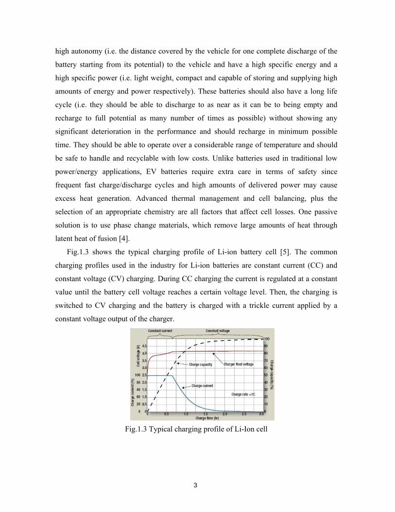
Fig.1.3 shows the typical charging profile of Li-ion battery cell [5]. The common
charging profiles used in the industry for Li-ion batteries are constant current (CC) and
constant voltage (CV) charging. During CC charging the current is regulated at a constant
value until the battery cell voltage reaches a certain voltage level. Then, the charging is
switched to CV charging and the battery is charged with a trickle current applied by a
constant voltage output of the charger.
Fig.1.3 Typical charging profile of Li-Ion cell

4
1.1.2 Charger Classifications
Since the inception of the first EVs, there have been many different charging systems
proposed. Due to many different configurations of the chargers, it is required to classify
them based on some common design and application features. Table1.1 [6] lists five
different methods of classifying chargers.
Table1.1: Battery charger classification
Classification type Options
Topology Dedicated, Integrated
Location On-board, Off-board
Connection type Conductive, Inductive, Mechanical
Electrical waveform AC, DC
Direction of power flow Unidirectional, Bidirectional
Power level Level1, Level2, Level3
The chargers can be classified based on the circuit topologies [7]. A dedicated circuit
solely operates to charge the battery. In comparison, the traction inverter drive can serve
as the charger at the same time when the vehicle is not working and plugged into the grid
for charging. This option is commonly known as integral/integrated chargers.
A second classification is the location of the charger. Carrying the charger on-board
greatly increases the charging availability of the vehicle. Off-board chargers can make use
of higher amperage circuits and can charge a vehicle in a considerably shorter amount of
time.
Fig.1.4 Block diagram of off-board charger
For off-board charger shown in Fig.1.4 [7], the charger is an external unit, rather than
a component of the EV. Furthermore an off-board charger produces a high DC voltage.
The internal battery management system (BMS) must be able to charge the battery using
this voltage. The major drawback of this topology is that the charger is not integrated in

5
the EV. Hence, it is impossible to charge the battery of an EV without an appropriate
charger which provides the needed high DC voltage on-site.
Fig.1.5 Block diagram of on-board charger
For on-board charger shown in Fig.1.5 [7], the charger is a component of the EV. The
EV can be charged almost everywhere using a single-phase or three-phase supply. The
major drawback of this topology is that this simple on-board charger requires an additional
DC/AC inverter. One inverter enables the vehicle-to-grid (V2G) capability and the second
drives the AC propulsion machine.
Third is the connection method [8]. Conductive charging contains metal to metal
contact, inductive charging connects ac grid to vehicle indirectly via a take-apart high
frequency transformer, and mechanical charging replaces the depleted battery pack with a
full one in battery swap stations.
Fourth, the electrical waveform at the connection port of the vehicle to the grid can be
either a dc connection or an ac connection [6]. Currently, the PHEVs and EVs in the
market employ an ac connection type. However, in the future the availability and
commonality of the dc sources may change the connection type.
Fifth, the charger can deliver power in unidirectional way by just charging the battery.
More advanced designs introduce bidirectional power transfer [9]. Again, all of the
chargers in the market employ unidirectional chargers.
Last, three charging levels have been defined for EVs and PHEVs [10]. These are
detailed in Table 1.2. Level 1 and level 2 charging are assumed to be the normal charging
levels which will take place where the vehicle will sit for a substantial amount of time
such as the home or office [11]. However, the drawback of charging a vehicle with these
normal charging levels is that it can take 4 to 20 hours depending on available power,
battery size and SOC of the battery [12] and this is not a viable option when long travel
distances are considered. The solution to this lengthy charging time issue is the level 3 fast
charging. Level 3 charging makes battery powered vehicles more competitive against

6
conventional ICE vehicles by charging the battery in less than 30 minutes [13]. Typically,
level 3 charging is accomplished via an off-board charger by means of converting three-
phase 480-V AC to a regulated DC. Although there have not been any adopted standards
for level 3 charging in the US [14] or internationally other than Japan [15], a Japanese
protocol known as CHAdeMO [16] is gaining international recognition. CHAdeMO
supplies the vehicle with a regulated DC voltage requiring an external charging station,
and interfaces directly with the vehicle battery and battery management system (BMS).
Alternatively, several European automakers are focusing on supplying vehicles directly
with 3-phase and processing it via an on-board battery charger [17].
Table 1.2: Battery charging levels
AC Voltage (V) Max. Current (A) Max. Power (kW) Level 1 120 16 1.92 Level 2 240 80 19.2 Level 3 300-600 400 240
1.2 Charger System
The charging time and lifetime of the battery have a strong dependency on the
characteristics of the battery charger [18]-[20]. Several manufacturers are working
worldwide on the development of various types of battery modules for electric and hybrid
vehicles. However, the performance of battery modules depends not only on the design of
modules, but also on how the modules are used and charged. In this sense, battery
chargers play a critical role in the evolution of this technology.
Fig.1.6 Battery charger system
The conventional battery charger system is shown in Fig. 1.6 [44]. Because batteries
have a finite energy capacity, PHEVs and BEVs must be recharged on a periodic basis,
typically by connecting to the power grid. The charging system for these vehicles consists
of an AC/DC rectifier to generate a DC voltage from the AC line, followed by a DC/DC
converter to generate the DC voltage required by the battery pack. Additionally, advanced
charging systems might also communicate with the power grid using power line
Battery Charger: AC/DC converter

7
communication (PLC) modems to adjust charging based on power grid conditions. The
battery pack must also be carefully monitored during operation and charging in order to
maximize energy usage and prolong battery life.
The focus of this thesis is to design and implement the DC-DC converter which
charges the high-voltage battery.
1.3 Charger System Requirements for Isolated DC-DC Converters
In EV applications, the propulsion battery is required to undergo a continuous
sequence of deep discharges followed by recharge to maximum capacity. The prime
requirement is therefore a system that provides a rapid and efficient charge, using as
simple equipment as possible and avoiding damage to the battery. The entire charging
process should be arranged in two phases. The first charging phase is at constant current
and with the battery voltage progressively rises. As soon as the battery voltage reaches the
trickle level, the constant-voltage charging method should be applied, with the charging
current progressively falling down to the maintenance level. The constant voltage charge
phase requires a decoupled and very accurate (i.e., close to 1/1000) measure of the battery
array voltage involving an expensive control system.
There are significant challenges associated with the design of the EV battery chargers,
such as high power density, high efficiency, low cost, isolation and voltage adaption while
complying with harsh environment automotive. Although the cost of passive elements can
usually be decreased by simply increasing the switching frequency, frequency is mostly
limited by the switching losses and turn on / turn-off time. Therefore, soft switching
methods and resonant circuits are widely used to increase the switching frequency [21].
Operating from a high input voltage requires a soft transition topology to minimize the
switching losses and reduce the high frequency EM1 caused by a high dv/dt. Another
challenge of such design is associated with the reverse recovery losses and the noise
caused by the high di/dt and dv/dt in the output rectifiers. And also it is necessary to
choose a topology that is also capable of controlling high output current.
In addition, galvanic isolation is required to disconnect grid from vehicle electrically.
Galvanic isolation can be achieved by means of using a high frequency (HF) transformer
integrated into DC-DC converter.

8
1.4 Conventional Isolated DC-DC Converters
1.4.1 Basic Isolated PWM Converters
The DC-DC converter topologies can be divided in two major parts: non-isolated and
insolated converter as tabulated in Table 1.2 [35], depending on whether or not they have
galvanic isolation between the input supply and the output circuitry. Isolated power
converter topologies can be classified as either single-ended or double-ended depending
on the usage of the B-H curve. During the operation, if the flux swings in only one
quadrant of the B-H curve, then the topology is classified as single-ended. If the flux
swings in two quadrants of the B-H curve, then the topology is classified as double-ended.
For a given set of requirements, a double-ended topology requires a smaller core than a
single-ended topology and does not need an additional reset winding. When designing an
isolated dc-dc power converter, the first and most critical choice is selection of the
topology. Historically, topology selection was based upon the desired output power level.
For the basic topologies, the order from lower power to higher power was usually flyback,
forward, push-pull, half-bridge and full-bridge.
The flyback may be the most commonly used isolated topology. It is generally found
in low cost, low power applications. Flyback topology requires only a single active switch
and does not require a separate output inductor in addition to the transformer. This makes
the topology easy to use and low cost. The disadvantages of the flyback topology are poor
transformer utilization, as it is a single-ended topology, and extra capacitors are required
at both the input and the output due to the high input and output ripple currents. The
forward and active clamp forward topologies are often employed in medium power
applications. The forward topology also suffers from poor transformer utilization due to
the limited duty cycle and as it is also single-ended topology. The active clamp forward
transformer does operate in two quadrants during steady state operation however peak flux
can reach high levels during startup and transient conditions. In order to reset the
transformer the maximum duty cycle is limited in both the forward topology and the
active clamp forward topology.
The remaining three topologies; push-pull, half-bridge and full-bridge are true double-
ended topologies whereby power transfer occurs in two quadrants of the BH curve and
does not require special provisions to reset the transformer. These double-ended

9
topologies are the best choice for applications where the highest power density is desired,
since the transformer core can be fully utilized. Another advantage of double-ended
topologies is the transformer can be further optimized because of the larger available duty
cycle range. Double-ended topologies can operate at a maximum duty cycle of almost
50% per side which equates to an effective maximum duty cycle of nearly 100% at the
output filter inductor. Designing the transformer turns ratio to maximize the effective duty
cycle greatly reduces the RMS current in the transformer and reduces the size of the
output filter.
For push-pull topology configuration, diodes D1 and D2 are shown for simplicity
however most modern, high efficiency power converters use synchronous MOSFETs as
secondary rectifiers. The push-pull topology has the advantage of being double-ended
however the peak voltage stress placed upon the primary switches during the off state is
very high, well over two times the input voltage.
The advantage of the half-bridge over the push-pull is the primary switch voltage
stress does not exceed the input voltage. Another advantage is there is only one primary
winding, allowing the transformer core window to be better utilized. The half-bridge
topology is only compatible with voltage-mode control. The ½Vin voltage balance at the
midpoint between C1 and C2 is not maintained with current-mode control or when
operating in cycle-by-cycle current limiting. Active midpoint balancing circuits can be
added to allow a half-bridge to operate with current-mode control; however these circuits
can be fairly complex.
For the full-bridge topology, it has all of the double-ended benefits. The primary
switch voltage does not exceed the input voltage. Transformer window utilization is very
good since there is only a single primary winding. When one of the primary switches is
active for the Half-Bridge topology the voltage across the primary winding is ½Vin. For
the Full-Bridge topology, the switches are activated as diagonal pairs. When a pair of
diagonal switches is active, the voltage across the primary winding is the full value of Vin.
Therefore for a given power, the primary current will be half as much for the Full-Bridge
as compared to the Half-Bridge. The reduced current enables higher efficiency as
compared to a Half-Bridge especially at high load currents.

10
Table 1.3: Power Supply Topologies from www.ti.com

11
The disadvantage of the full-bridge topology is the added complexity of driving four
primary switches and the cost of the additional switches. Relative to the Half-Bridge, part
of this additional cost is offset with reduction of input capacitors.
Another full-bridge configuration, which is used in high input voltage and high power
applications, is the phase-shifted full-bridge. This topology is similar to the conventional
full-bridge. However, the control methodology is different; the phase-shifted Full-Bridge
(PSFB) results in zero-voltage transitions of the primary switches while keeping the
switching frequency constant. Zero-volt switching is especially beneficial at high input
voltage applications. Often this topology needs an extra commutating inductor in series
with primary of the power transformer to ensure zero-volt switching at light load
conditions. A disadvantage of this topology is increased conduction losses in the primary
during the freewheeling time.
1.4.2 Basic Resonant Converters
Resonant converter, which were investigated intensively in the 80's [36]-[43], can
achieve very low switching loss thus enable resonant topologies to operate at high
switching frequency. In resonant topologies, Series Resonant Converter (SRC), Parallel
Resonant Converter (PRC) and Series Parallel Resonant Converter (SPRC, also called
LCC resonant converter) are the three most popular topologies. The analysis and design of
these topologies have been studied thoroughly.
1) Series Resonant Converter
The circuit diagram of a half bridge Series Resonant Converter is shown in Fig.1.7 (a)
[45]-[50] and the gain curve of SRC is shown in Fig.1.7 (b). The resonant inductor Lr and
resonant capacitor Cr are in series. They form a series resonant tank. The resonant tank
will then in series with the rectifier-load network. In this configuration, the resonant tank
and the load act as a voltage divider. By changing the frequency of driving voltage Vd, the
impedance of resonant tank will change. The input voltage is split between this impedance
and the reflected load. Since it is a voltage divider, the DC gain of SRC is always lower
than 1. At light-load condition, the impedance of the load is very large compared to the
impedance of the resonant network; all the input voltage is imposed on the load. This
makes it difficult to regulate the output at light load. Theoretically, frequency should be
infinite to regulate the output at no load.

12
(a) Circuit configuration (b) Gain curves
Fig.1.7 Half bridge SRC
When switching frequency is lower than resonant frequency, the converter will work
under zero current switching (ZCS) condition. When switching frequency is higher than
resonant frequency, the converter will work under zero voltage switching (ZVS)
condition. For power MOSFET, zero voltage switching is preferred. It can be seen from
the operating region that at light load, the switching frequency need to increase to very
high to keep output voltage regulated. This is a big problem for SRC. To regulate the
output voltage at light load, some other control method has to be added. As input voltage
increases, the converter is working at higher frequency away from resonant frequency.
As frequency increases, the impedance of the resonant tank is increased. This means
more and more energy is circulating in the resonant tank instead of transferred to output.
Here the circulating energy is defined as the energy send back to input source in each
switching cycle. The more energy is sending back to the source during each switching
cycle, the higher the energy needs to be processed by the semiconductors, the higher the
conduction loss. Also the turn off current is much smaller at lower input. When input
voltage increases, the turn off current is increased.
With above analysis, we can see that the major problems of SRC are: light load
regulation, high circulating energy and turn off current at high input voltage condition.
2) Parallel Resonant Converter
The schematic of parallel resonant converter is shown in Fig. 1.8 (a) [51]-[54] and its
gain curve is shown in Fig. 1.8 (b). For parallel resonant converter, the resonant tank is
still in series. It is called parallel resonant converter because in this case the load is in
parallel with the resonant capacitor. More accurately, this converter should be called series
resonant converter with parallel load. Since transformer primary side is a capacitor, an
inductor is added on the secondary side to match the impedance.
1S
2S oRoCinV
rC
acv−
+rL
oV−
+pN sN
TRdv
Square wave generator
Resonant networkRectifier network Voltage load
SRC
0 0.2 0.4 0.6 0.8 1 1.2 1.4 1.6 1.8 20
0.2
0.4
0.6
0.8
1
1.2
Q=0Q=1Q=2Q=3Q=4Q=5
Gain (2nVo/Vin)
fs/fr
Q=Zr/Ro
Q increasingRo decreasing
ZVS regionZCS region

13
(a) Circuit configuration (b) Gain curves
Fig.1.8 Half Bridge PRC
From the gain curves in 1.8 (b), Similar to SRC, the operating region is also designed
on the right hand side of resonant frequency to achieve Zero Voltage Switching. Compare
with SRC, the operating region is much smaller because the mountain is much steeper. At
light load, the frequency doesn't need to change too much to keep output voltage
regulated. So light load regulation problem doesn't exist in PRC. At high input voltage, the
converter is working at higher frequency far away from resonant frequency. Also from the
MOSFET current we can see that the turn off current is much smaller at lower input.
Compare with SRC, it can be seen that for PRC, the circulating energy is much larger.
For PRC, a big problem is the circulating energy is very high even at light load. Since the
load is in parallel with the resonant capacitor, even at no load condition, the input still see
a pretty small impedance of the series resonant tank. This will induce pretty high
circulating energy even when the load is zero.
The major problems of PRC are: high circulating energy, high turn-off current at high
input voltage condition.
3) Series Parallel Resonant Converter
The schematic of series parallel resonant converter is shown in Fig.1.9 (a). [55]- [57]
and the gain curve of SPRC is shown in Fig.1.9 (b). Its resonant tank consists of three
resonant components: Lr, Csr and Cpr. The resonant tank of SPRC can be looked as the
combination of SRC and PRC. Similar as PRC, an output filter inductor is added on
secondary side to match the impedance. For SPRC, it combines the good characteristic of
PRC and SRC. With load in series with series tank Lr and Csr, the circulating energy is
smaller compared with PRC. With the parallel capacitor Cpr, SPRC can regulate the output
voltage at no load condition.
1S
2S oRoCinV
rC
rL
oV−
+pN sN
TRdV
Square wave generator
Resonant networkRectifier network
fL
Current loadPRC
aci
0 0.5 1 1.5 2-0.5
0
0.5
1
1.5
2
2.5
3
3.5
4
fs/fr
SPRC Voltage Gain at Cn=1
Q=0.2Q=0.6Q=1Q=2Q=0Q=5
Gain(2nVo/Vin)
Q=Ro/Zr
Q decreasingRo decreasing
ZVS regionZCS region

14
(a) Circuit configuration (b) Gain curves
Fig.1.9 Half Bridge SPRC
Similar to SRC and PRC, the operating region is also designed on the right hand side
of resonant frequency to achieve Zero Voltage Switching. From the operating region
graph, it can be seen that SPRC narrow switching frequency range with load change
compare with SRC.
The input current is much smaller than PRC and a little larger than SRC. This means
for SPRC, the circulating energy is reduced compare with PRC.
Same as SRC and PRC, at high input voltage, the converter is working at higher
frequency far away from resonant frequency. Same as PRC and SRC, the circulating
energy and turn off current of MOSFET also increase at high input voltage.
With above analysis, we can see that SPRC combines the good characteristics of SRC
and PRC. Smaller circulating energy and not so sensitive to load change.
Unfortunately, SPRC still will see big penalty with wide input range design. With
wide input range, the conduction loss and switching loss will increase at high input
voltage. The switching loss is similar to that of PWM converter at high input voltage.
These three converters all cannot be optimized at high input voltage. High conduction
loss and switching loss will be resulted from wide input range.
4) LLC Resonant Converter
Three traditional resonant topologies analyzed above have a major penalty for wide
input range design. High circulating energy and high switching loss will occur at high
input voltage. There are some lessons learned from the above analyses. For a resonant
tank, working at its resonant frequency is the most efficient way. This rule applies to SRC
and PRC very well. For SPRC, it has two resonant frequencies. Normally, working at its
highest resonant frequency will be more efficient.
1S
2S oRoCinV
prC
rL
oV−
+pN sN
TRdV
Square wave generator
Resonant networkRectifier network
fL
Current loadSPRC
aci
srC
0 0.5 1 1.5 2-0.5
0
0.5
1
1.5
2
2.5
3
3.5
4
fs/fr
SPRC Voltage Gain at Cn=1
Q=0.2Q=0.6Q=1Q=2Q=0Q=5
Gain(2nVo/Vin)
Q=Ro/Zr
Q decreasingRo decreasing
ZVS regionZCS region

15
To achieve zero voltage switching, the converter has to work on the negative slope of
DC characteristic. From above analysis, SPRC resonant converter also could not be
optimized for high input voltage. The reason is same as for SRC and PRC; the converter
will work at switching frequency far away from resonant frequency at high input voltage.
Look at DC characteristic of SPRC resonant converter, it can be seen that there are two
resonant frequencies. One low resonant frequency determined by series resonant tank Lr
and Csr. One high resonant frequency determined by Lr and equivalent capacitance of Csr
and Cpr in series. For a resonant converter, it is normally true that the converter could
reach high efficiency at resonant frequency. For SPRC resonant converter, although it has
two resonant frequencies, unfortunately, the lower resonant frequency is in ZCS region.
For this application, we are not able to design the converter working at this resonant
frequency. Although the lower frequency resonant frequency is not usable, the idea is how
to get a resonant frequency at ZVS region. An LLC resonant converter could be
configured in Fig.1.10 (a) [58]-[60]. The DC characteristic of LLC converter is like a flip
of DC characteristic of SPRC resonant converter. There are still two resonant frequencies.
In this case, Lsr and Cr determine the higher resonant frequency. The lower resonant
frequency is determined by Cr and the series inductance of Lpr and Lsr. Now the higher
resonant frequency is in the ZVS region, which means that the converter could be
designed to operate around this frequency.
(a) Circuit configuration (b) Gain curves
Fig.1.10 Half Bridge LLC Resonant Converter
Applications in which the LLC converter is used can take advantage of these two main
features:
a. Narrow switching frequency range with light load and ZVS capability with even
no load, thus very low switching losses (high efficiency).
b. The capability to control the output voltage at all load and line conditions.
1S
2S oRoCinV
mL
rL
oV−
+pN sN
TRdV
Square wave generator
Resonant networkRectifier network Voltage load
LLC
rC
acv−
+pi
0.2 0.4 0.6 0.8 1 1.2 1.4 1.6
0
1
2
3
fs/fr
Gai
n(2n
Vo/V
in)
Gain Curves of LLC Resonant Converter at Lpr/Lsr= 2
2
53
1
0.5
0.3
0.1
0.7
12o r
r r
f fL Cπ
= =
( )1
2p
r m r
fL L Cπ
=+
of
pf
r
ac
ZQR
=
Q increasingRo decreasing

16
1.5 Topology Selection for EV Battery Charger
A topological overview of the different configurations used in EV power conversion
systems and general system block diagrams are presented in [61]-[65]. For the DC-DC
stage, many topologies can be considered as candidates. Among them, the most attractive
topologies are [22]-[24]:
1) A soft-switched full-bridge (FB) DC-DC converter;
2) An asymmetrically controlled zero-voltage switched (ZVS) half-bridge (HB)
converter;
3) An active-clamped soft-switched forward converter.
All these three DC-DC converters can achieve very high efficiency and very good
device utilization. Further selection of the dc-dc converter will depend on application
specifications, including power level, input line voltage, battery voltage, initial capital cost,
long term operation expense, and some economics and business philosophy.
Resonant converters are included in a wide range of converters. The strategy of using
one is to design a highly efficient converter while eliminating a common disadvantage of
traditional implementations based on Pulse-Width Modulation (PWM) – high switching
losses. Many different solutions have been suggested, implemented, and tested in recent
years, and many of them are now widely used in commercial products. Different battery
chargers based on resonant topologies have been reported in [25]–[27]. Generally
speaking, in order to guarantee ZVS in resonant converters, a high value of reactive
current circulation is required, particularly for a wide range of load variations. This leads
to a bulky resonant tank, lower power density, and lower efficiency.
Auxiliary commutated ZVS full-bridge converter topologies suitable for low-power
applications have been reported in [28] and [29] and further developed in [30]. In these
converters, an auxiliary circuit is used to produce the reactive current for the full-bridge
switches. The auxiliary circuit is working independent of the system operating conditions
and is able to guarantee ZVS from no load to full load. Although this topology seems very
suitable for the battery charger application, there are some setbacks related to the auxiliary
circuit. Since the auxiliary circuit should provide enough reactive power to guarantee ZVS
at all operating conditions, the peak value of the current flowing through the auxiliary
inductor is very high, which increases the MOSFET conduction losses drastically. Also,

17
due to the fact that the voltage and frequency across the auxiliary inductor are very high,
the core losses of this inductor are also high. In addition, too much reactive current leads
to large voltage spikes on the semiconductor switches due to the delay in the body diode
turn-on. [31] presents a control method, which optimizes the required reactive current
provided by the auxiliary circuit. The proposed control circuit adaptively controls the
reactive current required to guarantee ZVS under different load conditions. This leads to
significantly reduced semiconductor conduction losses as well as reduced auxiliary circuit
losses.
This thesis works on the power stage, presenting a hybrid phase-shifted full-bridge and
LLC resonant converter, which guarantees ZVS under any load conditions, and then gets it
further improved. This hybrid converter can achieve ZVS operation in the entire load
range by using the magnetizing inductance of the transformer. In addition, the converter
can operate with wide input-voltage variations without penalizing the efficiency.
Therefore, the converter is suitable for applications in which high efficiency and high
power density are required such as EV battery charger.
1.6 Thesis Outline
This thesis is divided into four chapters. They are organized as follows.
The first chapter is background of battery charger. Since the DC-DC converter is the
key element in battery charger system and this thesis mainly deals with the DC-DC
converter for EV battery charger, the isolated DC-DC converters are also simply
overviewed.
In second chapter, two basic types of DC-DC converters, which are applied in high
power application such as high voltage battery for electric vehicle, are analyzed
theoretically in detail.
The third chapter gives the novel converter topology for EV battery charger and its
corresponding detailed analysis. A 3.4 kW hardware prototype for battery charger has been
designed, fabricated and tested to verify the circuit validity and the improved performance
of the proposed converter.
In fourth chapter, an improved converter based on the one in chapter3 is developed and
analyzed theoretically.

18
CH2: Phase-Shifted Full Bridge and LLC Resonant
Converters for High Power Application
2.1 Introduction
In this chapter, two basic types of DC-DC converters, which are applied in high power
application such as high voltage battery for electric vehicle, are analyzed theoretically in
detail.
The full-bridge and half-bridge converters are mostly used in high power applications.
In both converters, the input voltage appears across the switching transistors. However,
they are required to carry twice as much current in the half–bridge converter. Therefore, in
high power applications, it may be advantageous to use a full bridge over a half bridge.
Efficiency, power density, reliability, and cost are important for the switched mode
power supply market. The effort to obtain ever-increasing power density of switched-
mode power supplies has been limited by the size of passive components. Operation at
higher frequencies considerably reduces the size of passive components, such as
transformers and filters. In order to achieve converters with high power densities, it is
usually required that they operate at higher switching frequencies, However, the high
transistor switching frequencies increase the total switching loss and lower the supply
efficiency. As switching frequencies increase, the switching losses associated with the
turn-on and turn-off of the devices also increases.
Therefore, zero voltage or zero current switching topologies allow for high frequency
switching while minimizing the switching loss. The ZVS topology operating at high
frequency can improve the efficiency and reduce the size and cost of the power supply
resulting in higher power densities. ZVS also reduces the stress on the semiconductor
switch, which improves the converter reliability. The Phase-Shifted ZVS Full Bridge
DC/DC Converter has become a very popular topology due to above advantages. [32]-
[33]analyzed the operation of the phase shift full bridge (PSFB) ZVS dc-dc converter. The
major problems are the high circulating current during normal operation, hard switching
on the secondary side and light load efficiency. In addition, due to duty cycle loss problem,
the effective duty cycle is even smaller. More conduction loss deteriorates the efficiency.

19
On the other hand, although soft switching is achieved at the primary side, hard switching
problems still remain for the secondary side devices. Switching loss and voltage stress of
secondary side devices are severe issues. At light-load conditions, ZVS may be lost. Thus,
the efficiency under light loads is another concern.
To reduce switching losses and allow high-frequency operation, resonant switching
techniques have been developed. In switch-mode PWM power supplies, the switching
losses can be high enough that they prohibit the operation of the power supply at very high
frequencies, even when soft-switching techniques are used. In resonant-mode power
supplies, however, the switching losses can be lower, allowing the resonant converter to
operate at higher frequencies [34]-[35]. Therefore, the use of resonant converters remains
an interesting option for some applications requiring high efficiency, high reliability, high
power density and low cost. These techniques process power in a sinusoidal manner and
the switching devices are softly commutated. Therefore, the switching losses and noise
can be dramatically reduced. For conventional PWM converters, LLC resonant converter
becomes the most attractive topology for medium power applications due to its high
efficiency and wide input range.
In general, LLC resonant converter can be employed in all applications with variable
input and output voltages, demand of high efficiency and power density as well as low
EMI. It exhibits superior performance, such as low switching loss and low voltage stress
on the secondary side rectifiers, as well as higher efficiency, than PWM converters. LLC
resonant converters can achieve ZVS from zero load to full load conditions. The LLC
resonant tank can be considered as a band pass filter, but the frequency selectivity of the
LLC tank is poor. For a resonant tank, working at its resonant frequency is the most
efficient way. Due to very wide bandwidth, the frequency has to be increased very high to
achieve enough voltage gain controllability. However, this is not practical for DC-DC
converters due to the limitation of driving circuits and the excessive switching & driving
losses.
Although there are some disadvantages in these two kinds of converters, they are widely
used in high power application. Next, the conventional phase shifted full bridge converter
and LLC converter will be discussed in detail in the following sections.

20
2.2 Phase Shifted Full Bridge Converter
When conventional PWM converters are operated at higher frequencies, the circuit
parasitics are shown to have detrimental effects on the converter performance. Switching
losses are especially pronounced in high-power, high-voltage applications. To achieve
ZVS, the two legs of the bridge are operated with a phase shift. This operation allows a
resonant discharge of the output capacitance of the MOSFETs, and, subsequently, forces
the conduction of each MOSFET’s anti-parallel diode prior to the conduction of the
MOSFET. It provides ZVS for the switches by using the leakage inductance of the
transformer and the output capacitance of the switches. It has a somewhat higher rms
current than the conventional full-bridge PWM converter, but has much lower rms
currents than the resonant converters. The ZVS allows operation with much reduced
switching losses and stresses, and eliminates the need for primary snubbers. It enables
high switching frequency operation for improved power density and conversion efficiency.
These advantages make this converter well suited for high-power, high-frequency
applications.
2.2.1 Topology Description
(a) Circuit configuration (b) Key operating waveforms
Fig.2.1 Phase-shifted Full bridge converter
Phase shift full bridge converter shown in Fig.2.1, as one of the most promising
topology for high frequency, high power application, has many good characteristics. It is a
soft switching converter. All four switches on primary side can achieve Zero Voltage
Switching (ZVS) with proper design. This is very helpful for high frequency operation.
This topology has lower volt-sec on the output filter inductor. Phase shift full bridge can
TR
secv oV−
+
−
+
1S
2S
1D
2D
oL
oRoC
inV
oi
pi3S
4S
lkL
3D
4DA B
0
0
0
0
0
0
ABv
secv
1G
2G
3G
4G
t
t
t
t
t
t
21
achieve smallest volt-sec for same design specification compared with two-switch forward
and half bridge converter. Another benefit of phase shift full bridge is its capability to
cover wide power range. For power from several hundred watts to kilowatts, full bridge
converter can perform very well. In recent years, even for low power application like
Voltage Regulator Module, full bridge topology has been investigated and showed
benefits.
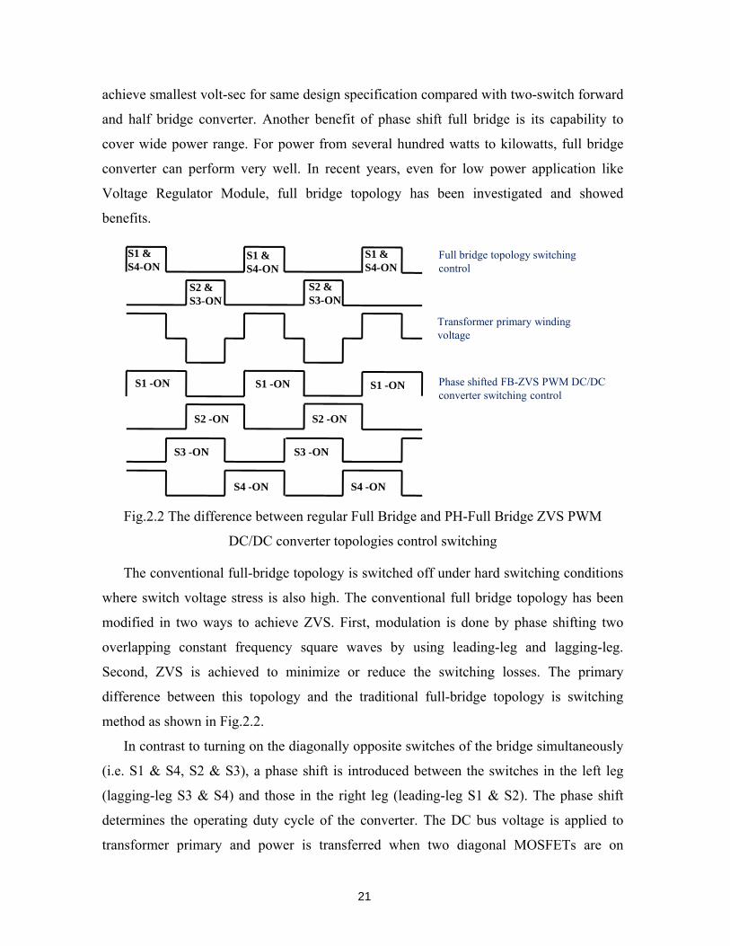
Fig.2.2 The difference between regular Full Bridge and PH-Full Bridge ZVS PWM
DC/DC converter topologies control switching
The conventional full-bridge topology is switched off under hard switching conditions
where switch voltage stress is also high. The conventional full bridge topology has been
modified in two ways to achieve ZVS. First, modulation is done by phase shifting two
overlapping constant frequency square waves by using leading-leg and lagging-leg.
Second, ZVS is achieved to minimize or reduce the switching losses. The primary
difference between this topology and the traditional full-bridge topology is switching
method as shown in Fig.2.2.
In contrast to turning on the diagonally opposite switches of the bridge simultaneously
(i.e. S1 & S4, S2 & S3), a phase shift is introduced between the switches in the left leg
(lagging-leg S3 & S4) and those in the right leg (leading-leg S1 & S2). The phase shift
determines the operating duty cycle of the converter. The DC bus voltage is applied to
transformer primary and power is transferred when two diagonal MOSFETs are on
Full bridge topology switching control
Transformer primary winding voltage
Phase shifted FB-ZVS PWM DC/DC converter switching control
S1 &S4-ON
S1 &S4-ON
S1 &S4-ON
S2 &S3-ON
S2 &S3-ON
S1 -ON S1 -ON S1 -ON
S2 -ON S2 -ON
S3 -ON S3 -ON
S4 -ON S4 -ON

22
simultaneously. When two high side switches or two low side switches are on
simultaneously (called freewheel state) the transformer primary is shorted. This results in
zero voltage across primary and secondary. The transformer primary current rising edge
slope as well as the falling edge slope reduces the duty cycle of the secondary voltage.
This reduces the output voltage of the DC/DC converter so transformer turns ratio is
effected and hence the secondary side power devices voltage. Llk and Lo affect this so their
values should be selected properly and effect should be analyzed.
2.2.2 Operating Modes
The schematic and operating waveforms of phase shift full bridge converter are
repeated in Fig.2.3. Based on this, operating modes are given.
(a) Circuit configuration (b) Key operating waveforms
Fig.2.3 Phase-shifted Full bridge converter
1) At time t1
• S4 turns off, S3 turns on, and S2 remains on.
• The equivalent capacitor Cs3 of S3 gets sinusoidal discharged and the equivalent
capacitor Cs4 of S4 gets sinusoidal charged by the leakage inductor (Llk ) current which
is relatively small. Thus, these two capacitors Cs3 and Cs4 are much harder to get fully
charged and discharged. S3 and S4 are much harder to be turned on at zero-voltage
condition. These two switches S1, S2 form the lagging leg in the circuit.
• The 4 diodes at the secondary side conduct.
• The transformer is shorted.
TR
secv oV−
+
−
+
1S
2S
1D
2D
oL
oRoC
inV
oi
pi3S
4S
lkL
3D
4DA B
0
0
0
0
ABv
secv
3G
4G
t
t
t
t
pi
0
0 1G
2G
t
t
1t 2t 3t 4t 5t
4
2
SD
3
2
DD 2 3S S
3
1
SD
4
1
DD 1 4S S
1I2I
p ea kI

23
Fig.2.4 Mode1: at time t1
2) At interval t1~t2
• The equivalent capacitor of S3 gets fully discharged and the equivalent capacitor of S4
gets fully charged. To make sure the equivalent capacitors get fully charged and
discharged, it requires a period of time during which both S3 and S4 are off. The period
is called dead time.
• The body diode D3 of S3 is on, which can make S3 turn on at zero-voltage condition.
• The 4 diodes at the secondary side are still conducting.
• The transformer is still shorted.
Fig.2.5 Mode2: at interval t1~t2
3) At interval t2~t3
• Llkis charged.
• The primary current switches from D2-D3 to S3-S2.
• The 4 diodes at the secondary side are still conducting.
• The transformer is still shorted.
0
0 ABv
secv
t
t
pi
1t 2t 3t 4t 5t
4
2
SD
3
2
DD 2 3S S
3
1
SD 4
1
DD
1 4S S
TRsecv oV
−
+
−
+
1S
2S
1D
2D
oL
oRoC
inVpi
3S
4S
lkL
3D
4D
A B
1sC
2sC
3sC
4sC
0
0 ABv
secv
t
t
pi
1t 2t 3t 4t 5t
4
2
SD
3
2
DD 2 3S S
3
1
SD 4
1
DD
1 4S S
TRsecv oV
−
+
−
+
1S
2S
1D
2D
oL
oRoC
inVpi
3S
4S
lkL
3D
4D
A B
1sC
2sC
3sC
4sC

24
Fig.2.6 Mode3: at interval t2~t3
4) At interval t3~t4
• Llk keeps charged.
• The output inductor Lo gets charged and the voltage at the secondary side vsec builds up.
• The energy is transferred to output load. This is power processing stage.
• The 2 diodes at the secondary side are conducting.
Fig.2.7 Mode4: at interval t3~t4
5) At interval t4
• S2 is turned off, S1 is turned on and S3 is still on.
• The equivalent capacitor (Cs1) of S1 gets linear discharged and the equivalent capacitor
(Cs2) of S2 gets linear charged by the output inductor (Lo ) current which is relatively
large. Thus, these two capacitors Cs1 and Cs2 are much easier to get fully charged and
discharged. S1 and S2 are much easier to be turned on at zero-voltage condition. These
two switches S1, S2 form the leading leg in the circuit.
• The voltage at the secondary side vsec drops. The circuit is going to freewheeling stage
from power processing stage.
• The 2 diodes at the secondary side are conducting at this moment.
0
0 ABv
secv
t
t
pi
1t 2t 3t 4t 5t
4
2
SD
3
2
DD 2 3S S
3
1
SD 4
1
DD
1 4S S
TRsecv oV
−
+
−
+
1S
2S
1D
2D
oL
oRoC
inVpi
3S
4S
lkL
3D
4D
A B
1sC
2sC
3sC
4sC
0
0 ABv
secv
t
t
pi
1t 2t 3t 4t 5t
4
2
SD
3
2
DD 2 3S S
3
1
SD 4
1
DD
1 4S S
TRsecv oV
−
+
−
+
1S
2S
1D
2D
oL
oRoC
inV
oi
pi3S
4S
lkL
3D
4D
A B
1sC
2sC
3sC
4sC

25
Fig.2.8 Mode5: at time t4
6) At interval t4~t5
• The equivalent capacitor of S1 gets fully discharged and the equivalent capacitor of S2
gets fully charged. To make sure the equivalent capacitors get fully charged and
discharged, it requires dead time between S1 and S2.
• The body diode D1 of S1 is on, which can make S1 is turned on at zero-voltage
condition.
• The voltage at the primary side vpri is clamped to zero.
• The 4 diodes at the secondary side are conducting.
Fig.2.9 Mode6: interval t4~t5
In order to avoid shoot through and ensure that S4 will turn-on with ZVS a dead time
is needed between the turn-off of S3 and turn-on of S4 and also make sure that diode D4
has started conducting. The resonance between Llk, Cs (Cs3//Cs4) and Ctr provides
sinusoidal voltage across S3 and D3 and this voltage peaks at one fourth of the resonant
period.
( )3 41 // //4 2peak lk s s trT L C C Cπτ = = (2.1)
0
0 ABv
secv
t
t
pi
1t 2t 3t 4t 5t
4
2
SD
3
2
DD 2 3S S
3
1
SD 4
1
DD
1 4S S
TRsecv oV
−
+
−
+
1S
2S
1D
2D
oL
oRoC
inV
oi
pi3S
4S
lkL
3D
4D
A B
1sC
2sC
3sC
4sC
0
0 ABv
secv
t
t
pi
1t 2t 3t 4t 5t
4
2
SD
3
2
DD 2 3S S
3
1
SD 4
1
DD
1 4S S
TRsecv oV
−
+
−
+
1S
2S
1D
2D
oL
oRoC
inVpi
3S
4S
lkL
3D
4D
A B
1sC
2sC
3sC
4sC

26
2.2.3 ZVS Process
Zero-voltage turn-on is achieved by using the energy stored in the leakage and series
inductance of the transformer to discharge the output capacitance of the switches through
resonant action. In order to achieve ZVS turn-on the energy stored in the leakage and
series inductance has to be larger than the energy stored in the output capacitances. The
resonance forces the body diode into forward conduction prior to gating on the switch.
Two different mechanisms exist which provide ZVS for the lagging-leg and leading leg.
a. ZVS for Lagging Leg
Fig.2.10 Detail of the rising edge of the voltage across the switch of lagging leg
where
(a) corresponds to the limit case when the energy in Llk is equal to the energy required
to charge the capacitances.
(b) corresponds to the case when the energy in Llk is larger than the energy required to
charge/discharge the capacitors. The switch output capacitances are
charged/discharged in less than one fourth of the resonant period, and the voltage
is clamped to the input voltage.
(c) corresponds to the case when the energy in Llk is not sufficient to charge/discharge
the output capacitances, and ZVS is lost.
During light loads, very little energy is stored in the primary side inductance Llk (can
be sum of the transformer leakage inductance and external inductance in series with the
primary of the transformer). This causes the lagging-leg to turn on under a hard switching
condition which can be seen from Fig.2.10 (c) and Loss of ZVS means extremely high
pi
0 ABv t3S
( / 2)D T
/ 2T
3D
0 0 0dt dt dt
pI
1I2I
( )a ( )b ( )c

27
switching losses at high switching frequencies and very high electromagnetic interference
(EMI) due to the high di/dt of the discharge current. Loss of ZVS can also cause a very
noisy control circuit, which leads to shoot-through and loss of the semiconductor switches.
As the load increases the energy stored in inductor Llk increases. This energy is used to
charge the output capacitance of the devices that are turning off, and to discharge the
output capacitance of the complementary device, thus forward biasing the freewheeling
diode. Full output capacitive discharge is necessary to cause the lagging-leg to start
turning-on under the ZVS condition. The turn-off under the ZVS condition closely mimics
that of resistive turn-off. A switch with low output capacitance helps to achieve ZVS
process at light load, improving the efficiency. Hard switching occurs when the output
capacitance of the switch requires more energy than is available in the inductance Llk to
fully charge and discharge the switches. And the energy stored available to turn on
lagging-leg the diode is very small so its conduction time is very small even at full load.
The energy stored in Llk increases by a square law as load current increases. Therefore, the
stored energy in Llk increases rapidly at loads higher than the minimum load required for
ZVS. The large amount of available charging energy causes the switch drain-source
voltage to rise and fall at a linear rate.
To achieve soft turn-on and turn-off of the lagging leg, the following equation should
be satisfied.
( )2 2 21 3 4
1 1 12 2 2lk s s in tr inL I C C V C V> + + (2.2)
Where Cs3, Cs4 is effective output capacitance of the power switches S3, S4 respectively. I1
is Primary transformer current at turn-on and turnoff for S3&S4. Ctr is transformer winding
capacitance.
Thus, the critical load at which ZVS is lost is
3 4//s s trZVS in
lk
C C CI VL
+= (2.3)
To make sure not to lose ZVS, the leakage inductance is adjusted to obtain a desired
value of IZVS

28
The lagging leg switch transition occurs due to resonance. The primary current during
this transition is sinusoidal with peak amplitude occurring at the start. Cs (Cs3//Cs4) and Llk
form the resonant tank and its oscillating frequency is given as follows.
( )3 4
1//
rlk s sL C C
ω = (2.4)
There must be enough time to get the output capacitor of the to-be turned on switch
fully discharged to make sure the switch can operate at ZVS condition. Meanwhile, the
discharge time should not be too long in case of another oscillating cycle starts, which is
clear in Fig.2.10 (b). The maximum discharge is at ¼ of the period as follows, which is
also graphically shown in Fig.2.10 (a).
( )max3 4
1 // //4 2d lk s s trt T L C C Cπ
= = (2.5)
b. ZVS for Leading Leg
For the leading-leg switches (S1& S2), a different process provides the ZVS as
explained below. Before S1 turns off, the current in the primary reaches its peak value of
the reflected filter inductor (Lo) current. When S1 is turned off, the energy available to
charge the output capacitance of S1 and to discharge the output capacitance of S2 is the
sum of the energy stored in the output filter inductor Lo and the primary side inductor Llk.
The energy stored in filter inductor Lo is available because the filter inductor current does
not freewheel through the diode until the voltage across the secondary has fallen to zero.
Fig.2.11 Detail of the rising edge of the voltage across the switch of leading leg
Accordingly, for soft turn on and turn-off of the leading leg the following equation
should satisfy.
pi
0 ABv t1S
( / 2)D T
/ 2T
1D
0
dt
pI1I
2I

29
( ) ( )2 2 2_ 2 1 2
1 1 1//2 2 2o p lk s s in tr inL L I C C V C V+ > + (2.6)
whereCs1, Cs2 is effective output capacitance of the power switches S1, S2respectively. I2 is
Primary transformer current at turn-on and turnoff for S1&S2. Ctr is transformer winding
capacitance. Lo_p is the output filter inductance referred to primary.
Since the stored energy in the output filter inductor is large when compared to that
required to charge and discharge the output capacitances of the leg and capacitance of the
transformer windings, the switch capacitance is charged and discharged at a linear rate.
The resulting leading leg transition time in liner ramp is given as
22
s sdv dvI C or dt Cdt I
= = (2.7)
Where 22
s sdv dvI C or dt Cdt I
= =
indv V= , which is input to the bridge and dt is switch transition time.
In this mode, even at lighter loads, much more stored energy is available to turn-on
and turn-off the leading-leg switches than is available for the lagging leg switches.
Therefore, the body diode in the leading leg turns on before the MOSFET is gated on even
at light loads. Since the energy stored in output filter is so high that a small snubber
capacitor can be put across leading leg switches and these devices can be turned off under
real ZVS condition. This will reduce the turn-off loss of these switches. The leading leg
free-wheeling diode (FWD) conduction duty cycle is higher than lagging led diodes so
leading-leg diodes will also dissipate a fair amount of power.
2.2.4 Relation between Duty Cycle, Transformer Turns Ratio and Switching
Frequency
Fig.2.12 shows the relationship between duty cycle, transformer turns ratio and
switching frequency for the phase-shifted full bridge converter.
( )
sec
sec
1 2 sec 2
4/2
o
in
eff pri
in lks
lk o
NVDV
D D D D
V LTD I I D fL N R
⎧⎪ =⎪⎪ = = −Δ⎨⎪
⎛ ⎞⎪Δ = + =⎜ ⎟⎪ ⎝ ⎠⎩
(2.8)

30
where N is the primary-to-secondary turns ratio; effD is effective duty cycle on the
secondary, that is secD ; DΔ is called duty cycle loss. Increasing lkL or sf will increase
DΔ . And since DΔ cannot exceed secD and sec _ max 1priD D D+ Δ < < , there is a limit on the
switching frequency. Although some drawbacks for phase shift full bridge, it is still a
popular topology. Its capability to operate at high frequency and wide power range enable
it to be used for multi applications.
Fig.2.12 Relation between duty cycle, transformer turns ratio and switching frequency
2.2.5 Disadvantages of Phase-shifted Full Bridge Converter
Fig.2.13 Key waveforms and formula of conventional PSFB converter
ZVS FULL-BRIDGE topology is the most popular topology used in the power range
of a few kilowatts (1–5 kW) for DC/DC converters [31]. Since the switch ratings are
optimized for the full-bridge topology, this topology is extensively used in industrial
applications. High efficiency, high power density, and high reliability are the prominent
features of this topology. But since ZVS in conventional full-bridge pulse width
modulation (PWM) converters is achieved by utilizing the energy stored in the leakage
pi0 ABv t
( / 2)D T
/ 2T( / 2)effD T
( / 2)D TΔ
/in o
o
V N VslopeNL
−=
/in lkslope V L=
pI1I
2I
o
o
VslopeNL−
=
pi
0 ABv t( / 2)D T
/ 2T( / 2)effD T
( / 2)D TΔ
/in o
f
V N VslopeNL
−=
/in lkslope V L=
pI1I
2I
o
f
VslopeNL−
=
Circulating current3 4
1//s s tr
ZVS inlk
C C CI I VL
+≥ =
sec 2
4 lks
o
LD D fN R
Δ =

31
inductance to discharge the output capacitance of the MOSFETs, the range of the ZVS
operation is highly dependent on the load and the transformer leakage inductance. It is
difficult to design a wide-operation-range PWM converter with high efficiency. According
to the key waveforms shown in Fig.2.13 of the phase-shifted full bridge converter, the
disadvantages are summarized as follows.
• It is not able to ensure ZVS operation at light loads. In battery charger applications,
ZVS is vitally important since the converter might be operating at absolutely no load
for a long period of time. In this application, when the battery is charged, the load is
absolutely zero, and the converter should be able to safely operate under the zero-load
condition.
• The magnitude of Llk of the transformer determines the ZVS load range and the ZVS
range can be extended by increasing the leakage inductance Llk. Since Llk limits the
rising and falling times of the primary currents, the available duty cycle in the
secondary is reduced. A large leakage inductance limits the power transfer capability
of the converter and reduces the effective duty ratio of the converter. This limits the
maximum Llk to be used in a particular design.
• The transformer turns ratio Ns/Np can be maximized to reduce the voltage stress of the
rectifiers. However, increasing Ns/Np reduces the primary current and consequently
increases the value of the Llk required for achieving a desired ZVS range.
• There is a limit on the switching frequency. Increasing the switching frequency also
increase the duty cycle loss.
• It has high circulating current during normal operation. During every switching cycle,
there is a time interval during which two up switches or low switches are turned on at
the same time. This will short the transformer primary side. During this time interval,
secondary is freewheeling and no energy transfer from input to output. Primary current
during this period is pretty high. This current circulates through the primary two
switches and transformer winding. This primary circulating current will increase
conduction loss and should be minimized to achieve high efficiency. The smaller the
duty cycle, the higher circulating current will be.

32
• Due to ZVS operation the primary side waveforms are free from switching noise and
require no snubber. The secondary voltage waveform for a high output voltage (360 V)
has a substantial ringing due to the reverse recovery of the diodes. The ringing
frequency is usually too close to the switching frequency which makes it difficult to
snub the ringing effectively using a RC snubber. An energy recovery snubber network
is employed to keep the snubber loss below 1% of the output power.
2.3 LLC Resonant Converter
Fig.2.14shows the circuit configuration of half bridge LLC resonant converter.With
variable frequency control, the voltage gain of LLC resonant converter can be controlled
as boost mode or buck mode. During the holdup time, the LLC resonant converter can
operate in boost mode. Thus, high voltage gain is achieved, which means that bulky
capacitors can be reduced considerably. Meanwhile, at the nominal condition, the LLC
resonant converter operates very close to the resonant frequency, which is the best
operation point to accomplish high efficiency. In addition, voltage gains of different Q
converge at the series resonant point. The LLC resonant tank parameters can be optimized
to achieve high efficiency for a wide load range. The LLC resonant converter is
considered as one of the most desirable topologies for wide input voltage range.
Fig.2.14 Half Bridge LLC Resonant Converter
LLC resonant converter has small switching loss. In LLC resonant converter,
magnetizing inductor current is used to realize ZVS and ZVS can be achieved from the
zero load to the full load conditions with small turnoff current. Therefore, zero turn-on
loss and small turn-off loss can be achieved. Furthermore, secondary side diode of LLC
resonant converter turns off with low di/dt. Thus, reverse recovery loss can be small on
1S
2S oRoCinV
mL
rL
oV−
+pN sN
T RdV
Square wave generator
Resonant networkRectifier network Voltage load
LLC
rC
acv−
+ri

33
secondary side. Combining smaller switching loss on both primary and secondary side,
LLC resonant converter efficiency is not sensitive to the switching loss and the circuit is
able to achieve high switching frequency operation.
Suppose / 1p sN N = , by using the same previous method discussed before, the
equivalent circuit for LLC in Fig.2.15 can be obtained and the voltage gain, M, can be
derived.
Fig.2.15 Equivalent Circuit for Half Bridge LLC Resonant Converter
By using the equivalent load resistance, the LLC AC equivalent circuit is obtained, as
illustrated in Fig.2.16 (a) and Fig.2.16 (b) shows how to obtain the equivalent load
resistance, Rac.
(a) Primary side AC equivalent circuit (b) Secondary side AC equivalent circuit
Fig.2.16 LLC Equivalent Circuit
By using exactly the same method as that applied in SRC,2
8Fac
ac oac
VR Ri π
= =
(Considering the transformer turns ratio ( /p sn N N= ), the equivalent load resistance is
2
2
8Fac
ac oac
V nR Ri π
= = ), and according to the LLC AC equivalent circuit of Fig.2.16 (a), the
LLC voltage gain, M, is obtained as: 2
,
2 2,
2 2
4 ( 1)
4/ 21 1 ( 1)2
F oac pk oo
Finin d pk
p o o
mVvVM VV vj m Q
ωωπ
ω ω ωπ ω ω ω
⎛ ⎞−⎜ ⎟
⎝ ⎠= = = =⎛ ⎞ ⎛ ⎞
− + − −⎜ ⎟ ⎜ ⎟⎜ ⎟ ⎝ ⎠⎝ ⎠
(2.9)
where 1 1, , , , , .p r rp m r r o p
r r ac r r p r
L L ZL L L m Z QL C R L C L C
ω ω= + = = = = =
rCrL
dV
−
+
a cv
−
+oV
oV−mLinV
0
rCrL
Fdv F
acv−
+acR
−
+oRoC
oV−
+
acvaci +−
oI
mL
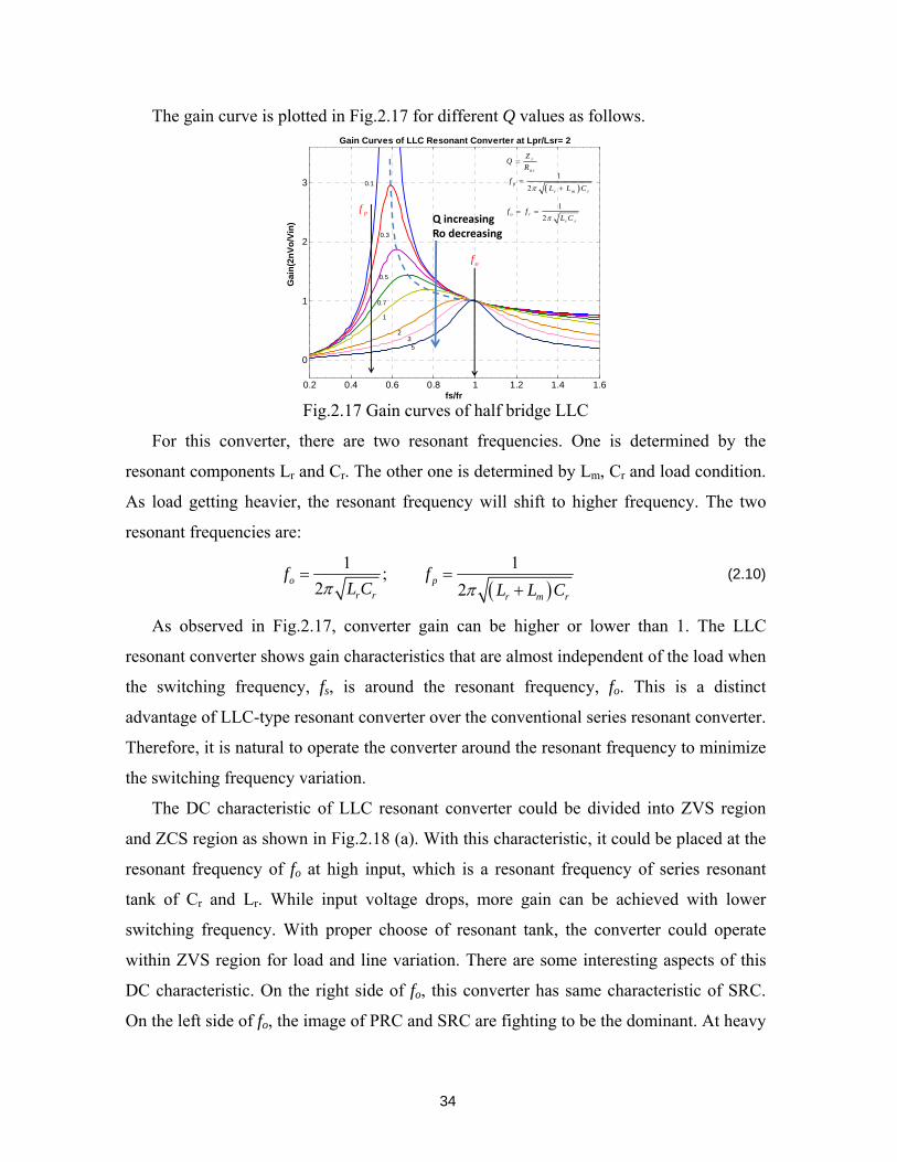
34
The gain curve is plotted in Fig.2.17 for different Q values as follows.
Fig.2.17 Gain curves of half bridge LLC
For this converter, there are two resonant frequencies. One is determined by the
resonant components Lr and Cr. The other one is determined by Lm, Cr and load condition.
As load getting heavier, the resonant frequency will shift to higher frequency. The two
resonant frequencies are:
( )1 1;
2 2o p
r r r m r
f fL C L L Cπ π
= =+
(2.10)
As observed in Fig.2.17, converter gain can be higher or lower than 1. The LLC
resonant converter shows gain characteristics that are almost independent of the load when
the switching frequency, fs, is around the resonant frequency, fo. This is a distinct
advantage of LLC-type resonant converter over the conventional series resonant converter.
Therefore, it is natural to operate the converter around the resonant frequency to minimize
the switching frequency variation.
The DC characteristic of LLC resonant converter could be divided into ZVS region
and ZCS region as shown in Fig.2.18 (a). With this characteristic, it could be placed at the
resonant frequency of fo at high input, which is a resonant frequency of series resonant
tank of Cr and Lr. While input voltage drops, more gain can be achieved with lower
switching frequency. With proper choose of resonant tank, the converter could operate
within ZVS region for load and line variation. There are some interesting aspects of this
DC characteristic. On the right side of fo, this converter has same characteristic of SRC.
On the left side of fo, the image of PRC and SRC are fighting to be the dominant. At heavy
0.2 0.4 0.6 0.8 1 1.2 1.4 1.6
0
1
2
3
fs/fr
Gai
n(2n
Vo/V
in)
Gain Curves of LLC Resonant Converter at Lpr/Lsr= 2
2
53
1
0.5
0.3
0.1
0.7
12o r
r r
f fL Cπ
= =
( )1
2p
r m r
fL L Cπ
=+
of
pf
r
ac
ZQR
=
Q increasingRo decreasing

35
load, SRC will dominant. When load get lighter, characteristic of PRC will floating to the
top. With these interesting characteristics, we could design the converter working at the
resonant frequency of SRC to achieve high efficiency. Then we are able to operate the
converter at lower than resonant frequency of SRC still get ZVS because of the
characteristic of PRC will dominant in that frequency range. From above discussion, the
DC characteristic of LLC resonant converter could be also divided into three regions,
region 1 and region 2 and Region 3, according to different mode of operation as shown in
Fig.2.18 (b).
(a) (b)
Fig.2.18 Operating Regions for LLC Resonant Converter
(a) At given Lm/Lr (b) At given Q
Fig.2.19 DC Characteristic of LLC Resonant Converter
The operating range of the LLC resonant converter is limited by the peak gain
(attainable maximum gain), which is indicated with “·” and connected as the boundary of
ZVS and ZCS in Fig.2.18 (a). It should be noted that the peak gain does not occur at fo
0.4 0.6 0.8 1 1.2 1.40
0.5
1
1.5
2
2.5
3
fs/fr
Volta
ge G
ain
(Vo/
Vin)
DC Characteristic of LLC Resonant Converter
Q=0.1Q=0.3Q=0.5Q=0.7Q=1Q=2Q=3Q=5
ZCS Region
ZVS Region
0.4 0.6 0.8 1 1.2 1.40
0.5
1
1.5
2
2.5
3
fs/fr
Volta
ge G
ain
(Vo/
Vin)
DC Characteristic of LLC Resonant Converter
Q=0.1Q=0.3Q=0.5Q=0.7Q=1Q=2Q=3Q=5
ZCS Region
ZVS Region
Region 1
Region 2
Region 3
0.2 0.4 0.6 0.8 1 1.2 1.4 1.60
0.5
1
1.5
2
2.5
3
fs/fo
Volta
ge G
ain
(Vo/
Vin)
Gain Curves of LLC Resonant Converter at Lm/Lr= 4
Q=0.1Q=0.3Q=0.5Q=0.7Q=1Q=2Q=3Q=5
Q increasingPeak gain decreasing
of
0.2 0.4 0.6 0.8 1 1.2 1.4 1.60
0.5
1
1.5
2
fs/fo
Volta
ge G
ain
(Vo/
Vin)
Gain Curves of LLC Resonant Converter at Q=0.33
m=3m=4m=5m=6m=7m=8m=9m=10
m=Lm/Lr
m increasingPeak gain decreasing
of

36
nor fp. The peak gain frequency where the peak gain is obtained exists between fp and fo, as
shown in Fig.2.18 (a). As Q decreases (as load decreases), the peak gain frequency moves
to fp and higher peak gain is obtained. Meanwhile, as Q increases (as load increases), the
peak gain frequency moves to fo and higher peak gain drops; thus, the full load condition
should be the worst case for the resonant network design. And from Fig.2.19, it can be
seen that the voltage gain is unity at resonant frequency, fo, regardless of the Q or m
variation.
The converter should be prevented from entering region 3 which is ZCS region, as
illustrated with one gain curve in Fig.2.20.
Fig.2.20 The switching frequency vs. the peak gain frequency
Above the peak gain frequency also called here inductive region, the input impedance
of the resonant tank is inductive and the input current of the resonant network (ip) lags the
voltage applied to the resonant tank (Vd). This permits the MOSFETs to turn on with zero
voltage (ZVS). Meanwhile, the input impedance of the resonant tank becomes capacitive
and the input current of the resonant network (ip) leads the voltage applied to the resonant
tank (Vd). below the peak gain frequency also called here capacitive region. When
operating in capacitive region, the MOSFET body diode is reverse recovered during the
switching transition, which results in severe noise. Another problem of entering into the
capacitive region is that the output voltage easily becomes out of control since the slope of
the gain is reversed.
Due to different operation mode of LLC resonant converter, its operation principles
are quite complex. According to its switching frequency, LLC operation modes can be
separated into above, below and equal to the resonant frequency.
2.3.1 Switching Frequency Equal to Resonant Frequency
For conventional resonant converters, such as SRC and PRC, it is desired to make the
converter operate at the resonant frequency to maximize the circuit efficiency. However,
sf
( )Gain M
inductive regioncapacitiveregion peak gain
ZCS region ZVS region

37
when these circuits operate on the left hand side of resonant frequency, circuits work
under zero current switching. To ensure ZVS operation enough design margins has to be
considered during design stage. Thus, the circuit would not be able to operate at the
optimal operation point. For LLC resonant converter, ZVS switching can be achieved for
the switching frequency either higher or lower than the resonant frequency. Thus, there is
no such requirement for the design margin, and the circuit is able to operate at the resonant
frequency while achieving optimal efficiency. For the circuit diagram shown in Fig.2.21
(a), operating principle at resonant frequency can be demonstrated in Fig.2.21 (b) and the
corresponding topological modes can be summarized as in Fig.2.21 (c).
(a) Topology; (b) Key waveforms; (c) Topological modes
Fig.2.21 LLC converter operating at resonant frequency
At interval between t0 and t1, switch S1 is conducting. In this period, the resonant tank
current is larger than the magnetizing inductor current. According to the polarity of the
transformer, secondary diodes D1 and D4 are conducting. Therefore, voltage applied to the
transformer magnetizing inductance is the output voltage reflected to transformer primary
side. Thus, magnetizing current linearly increases. During this period, the difference
between the input voltage and output voltage is applied to the resonant tank, and resonant
tank current is a sinusoidal waveform. At time t1, resonant tank current reaches
1_g sV _ 2g sV
dV
miri
seci
t
t
t
t
0t 1t2t
3t
1S
2S oRoCinV
mL
rL
oV−
+pN sN
T R
dV rCseci
1S
2S oRoCinV
mL
rL
oV−
+pN sN
TR
dV rC
2sC
1sC
oV
1S
2S oRoCinV
mL
rL
−
+pN sN
T RdV rC seci
1S
2S oRoCinV
mL
rL
oV−
+pN sN
TRdV rC
ri
mi
seci( )0 1~t t
( )1 2~t t
( )2 3~t t
( )a
( )b ( )c
1D
2D
3D
4D
1D
4D
2D
3D

38
magnetizing current and S1 turns off. At interval t1 and t2, secondary diodes are off,
because the resonant tank current is the same as magnetizing current and there is no
current transferred to load. Due to the junction capacitors of S1 and S2, magnetizing
current discharges the capacitors and help to achieve ZVS turn on of S2. Both S1 and S2
are off. This period is known as the dead-time, which is used to allow enough time to
achieve ZVS, as well as prevent shoot through of two switches. At time t2, S2 turn on with
zero voltage switching. At interval between t2 and t3, the difference between the resonant
tank current and the magnetizing inductor current is transferred to load. After t3, S2 is turn
off and circuit operates into another half cycle. At resonant frequency, LLC resonant
converter is able to achieve ZVS turn on for the primary side switches. Meanwhile, the
switching turn-off current is maximum transformer magnetizing inductor current. By
choosing a suitable magnetizing inductor, small turn-off loss can be realized. Moreover,
secondary diodes turn off with low di/dt, which means smaller reverse recovery loss.
Therefore, at resonant frequency, optimal performance of LLC resonant converter is
expected. At resonant frequency, the series resonant tank impedance is equal to zero.
Therefore, the input and output voltages are virtually connected together. Thus, the
voltage gain at resonant frequency is equal to 1.
2.3.2 Switching Frequency Lower Than Resonant Frequency
When the switching frequency of LLC resonant converter is lower than the resonant
frequency, magnetizing inductor participates in the circuit operation, which modifies the
converter voltage gain characteristics. The equivalent circuit and key waveforms are
shown in Fig.2.22 and the topological modes are shown in Fig.2.23.
(a) Topology (b) Key waveforms
Fig.2.22 LLC converter operating at lower resonant frequency
At interval between t0 and t1, switching S1 and diodes D1and D4 are conducting, and
the converter deliveries energy to load. At time t2, the resonant tank current resonates back
1_g sV _ 2g sV
dV
miri
seci
t
t
t
t
0t 1t2t
3t
1S
2S oRoCinV
mL
rL
oV−
+pN sN
TRdV rC
ri
mi
seci1D
2D
3D
4D 4t

39
with a magnitude equal to the magnetizing current. After that, the magnetizing inductor
begins to participate in the resonance. Since the resonant current is equal to magnetizing
inductor current, the secondary diodes are turned off. At interval between t2 and t3, S1turns
off and the magnetizing inductor transfers its stored energy to the resonant capacitor.
Therefore, in this operation mode, the converter is able to boost the gain up. And the
junction capacitors Cs1, Cs2 of the switches get fully charged and discharged before t3.
Then resonant tank transfers to the body diode of S2. Thus S2 achieves ZVS turn on. At
interval t3 and t4, circuit enters the other half cycle.
Fig.2.23 Topological modes for LLC converter operating at lower resonant frequency
2.3.3 Switching Frequency Higher Than Resonant Frequency
When LLC resonant converter operates with switching frequency higher than the
resonant frequency, the circuit operates as a SRC circuit. The equivalent circuit and key
waveforms are shown in Fig.2.24 and the topological modes shown in Fig.2.25,
respectively.
(a) Topology (b) Key waveforms
Fig.2.24 LLC converter operating at higher resonant frequency
1S
2S oRoCinV
mL
rL
oV−
+pN sN
T R
dV rCseci
oV
1S
2S oRoCinV
mL
rL
−
+pN sN
T RdV rC seci
( )0 1~t t
( )3 4~t t
( )a
1D
4D
2D
3D
( )c ( )d
( )b
1S
2S oRoCinV
mL
rL
oV−
+pN sN
T R
dV rC( )1 2~t t
1S
2SinV
mL
rLdV rC
2sC
1sC ( )2 3~t t
oRoCoV−
+pN sN
TR4D
1_g sV _ 2g sV
dV
miri
seci
t
t
t
t
0t 1t2t
3t
1S
2S oRoCinV
mL
rL
oV−
+pN sN
T RdV rC
ri
mi
seci1D
2D
3D
4D4t

40
At interval t0 and t1, switch S1 is conducting and the circuit is transferring energy to
load through diode D1 and D4. At time t1, S1 is turned off. Because the switching
frequency is higher than resonant frequency, the resonant tank current is higher than the
magnetizing current. At interval between t1 and t2, both S1 and S2 are off, the resonant tank
current is charging and discharging the junction capacitors of primary side switches. At
time t2, voltage on junction capacitor of switch S2 is discharged to zero. At interval
between t2 and t3, the body diode of switch S2 is turned on, the resonant tank current
decreases quickly. At time t3, the resonant tank current is equal to magnetizing current and
diodes D1 and D4 turn off. At interval t3 and t4, S2 can be turned on with zero voltage
switching and diodes D2 and D3 turn on and the circuit begins to transfer energy to load. In
this operation mode, ZVS switching on primary side switches can be guaranteed due to the
large turn off current. However, the large turn off current generates excessive turn-off loss
on the primary side switches. Moreover, the secondary side diode turns off with large
di/dt, which can cause large reverse recovery on the diodes. Furthermore, the high di/dt
turn off of the diodes cause extra voltage stress on the diode, which makes the circuit less
reliable.
Fig.2.25 Topological modes for LLC converter operating at higher resonant frequency
From previous analysis, it can be seen that LLC resonant converter is able to achieve a
larger gain below resonance operation, smaller above resonance operation or equal to 1 at
resonance operation. When the circuit operates at resonant frequency, the converter
voltage gain is equal to one, and circuit operates optimally. Operation below the resonant
1S
2S oRoCinV
mL
rL
oV−
+pN sN
T R
dV rCseci
1S
2SinV
mL
rLdV rC
2sC
1sC
oV
1S
2S oRoCinV
mL
rL
−
+pN sN
T RdV rC seci
( )0 1~t t ( )1 2~t t
( )3 4~t t
( )a
1D
4D
2D
3D
oRoCoV−
+pN sN
T R
seci1D
4D
mL
rLrC
2sC
( )2 3~t t
oRoCoV−
+pN sN
T R
seci1D
4D
1S
2SinV dV
( )c ( )d
( )b

41
frequency allows the soft commutation of the rectifier diodes in the secondary side, while
the circulating current is relatively large. The circulating current increases more as the
operation frequency moves downward from the resonant frequency. Below resonance
operation also has a narrow frequency range with respect to the load variation since the
frequency is limited below the resonant frequency even at the no-load condition.
Operation above the resonant frequency allows the circulating current to be minimized,
but the rectifier diodes are not softly commutated such that the reverse recovery loss might
be severe. Above resonance operation has less conduction loss than the below resonance
operation. However, operation at above the resonant frequency may cause too much
frequency increase at light-load condition.
2.3.4 Design Considerations of LLC Resonant Converter
Since LLC resonant converter operates with switching frequency higher than resonant
frequency, the circuit operates as a SRC circuit which cannot demonstrate the benefits of
LLC resonant converter. In this case, ZVS switching on primary side switches can be
guaranteed due to the large turn off current but it is very difficult to regulate the output at
light load. Therefore, the LLC resonant converter is always designed to operate at region2,
which is below or equal to the resonant frequency but in ZVS region.
a. Determine Transformer Turns Ratio n
By choosing a suitable transformer turns-ratio, LLC resonant converter could operate
with resonant frequency at normal condition and achieve high efficiency. Since at the
resonant frequency, the converter voltage gain is equal to 1. To allow LLC converter
operating with resonant frequency at normal condition, transformer turns-ratio in turn
requires meeting the equation
o
in
VnV
= (2.11)
In this equation, Vo is the desired output voltage, Vin is the resonant tank input voltage
at normal operation condition, which is equal to the bus voltage for full bridge structure
and is equal to half of the bus voltage for half bridge structure.
b. ZVS Operation
In region 2, to achieve ZVS, there should be enough dead-time during which both
switches S1 and S2 are off and duty cycle loss occurs because no power is delivered to load.

42
Fig.2.26 shows how to get enough dead-time to guarantee ZVS, where Cs1 and Cs2 is the
equivalent output junction capacitance of S1 and S2, respectively.
Fig.2.26 Dead-time requirement
To realize ZVS, the turn-off current should be able to discharge and charge the
junction capacitors during dead-time. It requires the turn-off current is smaller than the
maximum current of the magnetizing inductor, thus,
1 21 2 _ max 4
cs cs os s r Lm
m
du du nV TC C i Idt dt L
+ = ≤ = (2.12)
So the dead-time should meet
( )1 18dead m s s st L C C f≥ + (2.113)
c. Determine Magnetizing Inductance
Given the dead-time and switching frequency, to achieve ZVS it requires the
magnetizing inductance to meet
( )1 18dead s
ms s
t TLC C
≤+
(2.14)
Comparing with series resonant converter, LLC resonant largely reduces the
magnetizing inductance. In this way, the magnetizing inductor can be used to realize soft
switching for primary side switches. Furthermore, the magnetizing inductor participates
into the resonance and modifies voltage gain characteristic. Lm needs to be designed very
properly. Switching loss is a controlled parameter. the turn-off current of primary
switching is determined bythe choice of resonant inductor Lm.Alarger Lm can produce less
magnetizing current and less circulating energy, and RMS current can be minimized. But a
larger Lm can lead to smaller attainable maximum voltage gain, causing the output voltage
not able to be regulated to meet the desired requirements.
d. Determine the Ratio /m rL L
1_g sV _ 2g sV
miri
t
t
deadt
1S
2SinV
2sC
1sC
( )a
_ maxLmI_ maxLmIdsv
( )b
_ max 4o
Lmm
nV TIL
=
dsv
1csv−+
2csv+−
ri

43
While determining the maximum gain (Attainable Maximum Gain), the ratio m
(m=Lm/Lr) and Q need to be chosen properly.
From Fig.2.27, it shows that higher peak gain can be obtained by reducing Q or m
values. With a given resonant frequency (fo) and Q value, decreasing m means reducing
the magnetizing inductance, which results in increasing circulating current. Accordingly,
there is a trade-off between the available gain range and conduction loss. However, once
magnetizing inductor is chosen, the relationship between Ln and Q has been fixed. From
the definition of mand Q, their product is
2r
rm om
r o o
LCL fm Q L
L R Rπ
= =i i (2.15)
Fig.2.27 Peak Gain vs Q for different m values
Once converter specification is defined and switching frequency is chosen, the product
of m and Q is only determined by the magnetizing inductor. Therefore, for the designed
magnetizing inductor, the product of m and Q is set. Usually small m and large Q is
preferred to get narrower fs operation range which can be observed from Fig.2.19.
e. Maximum Operation Gain
The minimum switching frequency should be well limited above the peak gain
frequency, which can be referred to Fig.2.28.
The available input voltage range of the LLC resonant converter is determined by the
peak voltage gain. Thus, the resonant tank should be designed so that the gain curve has
0.2 0.4 0.6 0.8 1 1.2 1.41
1.1
1.2
1.3
1.4
1.5
1.6
1.7
1.8
1.9
2
2.1
2.2
2.3
2.4
2.5
Q
Pea
k G
ain
Peak Gain vs Q for Different m Values
m increasingPeak Gain decreasing
m=2m=2.5m=3m=3.5m=4m=5m=6m=7m=8m=9
m
r
LmL
=

44
an enough peak gain to cover the input voltage range. However, ZVS condition is lost
below the peak gain point as depicted in Fig.2.28. Therefore, some margin is required
when determining the maximum gain to guarantee stable ZVS operation during the load
transient and start-up. Typically 10~20% of the maximum gain is used as a margin for
practical design, as shown in Fig.2.28.
Fig.2.28 Determining the Maximum Gain
2.3.5 Disadvantages of LLC Resonant Converter
LLC is very attractive to overcome the issues of conventional circuits. With LLC
resonant converter, performance at high input voltage could be optimized and the
converter still could cover wide input voltage range. Fig.2.29 illustrates the key
characteristics and formula of half-bridge LLC converter under ZVS conditions.
• Operation below the resonant frequency allows the soft commutation of the rectifier
diodes in the secondary side, while the circulating current is relatively large. The
circulating current increases more as the operation frequency moves downward
from the resonant frequency.
• Larger m leads to wider frequency range. To get the frequency range narrower, m
can be reduced. Decreasing m means reducing magnetizing inductance, Lm, which
results in increased circulating current, thus, switching loss and conduction loss will
increase. And larger Lm means larger duty cycle loss because there is no power
delivery during deadtime.
• Since the product of m and Q is fixed once Lm and switching frequency are given,
smaller m and larger Q is preferred to get narrower frequency range but results in
smaller attainable peak gain. The problem with switching frequency lower than
sf
( )Gain M
of
max10 ~ 20% of MmaxM
peak gainmaximum operation gain( )

45
resonant frequency is the conduction loss will increase as switching frequency
drops.
(a) DC characteristics of half bridge LLC
(b) Peak Gain vs Q for different m values and key formula for half bridge LLC
Fig.2.29 Key characteristics and formula of HB LLC converter
• For same specification, Lr and Cr can have different values, which will work. Although there is a limit on how small Cr can be in order to keep Q reasonable, Cr can be chosen larger, which makes smaller voltage stress on Cr, but the impedance of the resonant tank will be small too. With smaller tank impedance, the short circuit current will be higher and higher switching frequency is needed to limit the output current, which will affect the short circuit performance.
0.2 0.4 0.6 0.8 1 1.2 1.4 1.60
0.5
1
1.5
2
fs/fo
Volta
ge G
ain
(Vo/
Vin)
Gain Curves of LLC Resonant Converter at Q=0.33
m=3m=4m=5m=6m=7m=8m=9m=10
m=Lm/Lr
m increasingPeak gain decreasing
of
0.2 0.4 0.6 0.8 1 1.2 1.4 1.60
0.5
1
1.5
2
2.5
3
fs/fo
Volta
ge G
ain
(Vo/
Vin)
Gain Curves of LLC Resonant Converter at Lm/Lr= 4
Q=0.1Q=0.3Q=0.5Q=0.7Q=1Q=2Q=3Q=5
Q increasingRo decreasingPeak gain decreasing
of
12o
r r
fL Cπ
=
r
ac
ZQR
=
Border line
0.2 0.4 0.6 0.8 1 1.2 1.41
1.1
1.2
1.3
1.4
1.5
1.6
1.7
1.8
1.9
2
2.1
2.2
2.3
2.4
2.5
Q
Pea
k G
ain
Peak Gain vs Q for Different m Values
m increasingPeak Gain decreasing
m=2m=2.5m=3m=3.5m=4m=5m=6m=7m=8m=9
m
r
LmL
=
2r
rm om
r o o
LCL fm Q L
L R Rπ
= =i i
( )1 28dead s
ms s
t TLC C
≤+
_ max 4o
Lmm
nV TIL
=
( )1 28dead m s s st L C C f≥ +

46
CH3: Hybrid Resonant and PWM Converter
3.1 Motivations
From the previous chapter 2, it can be concluded that the phase shifted full bridge
converter and LLC half-bridge resonant converter have their own merits and demerits,
some of which are considered important for EV battery charger and summarized in Table
3.1, and none of the two are perfect.
Table 3.1: Phase-Shifted Full Bridge vs. LLC Converters
Control method
ZVS range
Circulating current
Constant Current and
Voltage
Output diode voltage stress
PS FB Fixed frequency
Limited range High Yes High
LLC Variable frequency
Full range Low No Low
Note: PS FB represents phase-shifted full bridge converter; LLC represents LLC converter.
In battery charger applications, ZVS is vitally important since the converter might be
operating at absolutely no load for a long period of time. In this application, when the
battery is charged, the load is absolutely zero, and the converter should be able to safely
operate under the zero-load condition. From this view, the phase-shifted full bridge
converter is very hard to meet this requirement. LLC seems a good candidate, but the
variable frequency control makes it very complicated to handle all the conditions, and it is
not easy to regulate the output current, which cannot meet the constant current charging
requirement for EV battery charger.
So, what if they are hybrid together? Let LLC operate at fixed frequency very close to
the resonant frequency, which is the best operating point to accomplish high efficiency. It
can achieve ZVS from zero load to full load which is very vital in the battery charger
system. It seems a good idea to make LLC solve soft switching problem and make the
phase-shifted full bridge converter adjust the output voltage and the power levels.
3.2 Proposed Hybrid Resonant and PWM Converter
A novel Hybrid Resonant and PWM Converter in Fig.3.1is presented to keep the
advantages of high efficiency and small output inductance. The major features of the

47
hybrid resonant and PWM converter are as follows: 1) zero-voltage switching of
MOSFETs in the leading-leg can be achieved from true zero to full load because of the
parallel LLC resonant half-bridge configuration; 2) zero-current switching of IGBTs in the
lagging-leg is realized in full line and load range with minimum circulating conduction loss
due to effectively resetting of the parallel secondary-side constant DC voltage source; 3)
duty cycle loss is negligible since the ZVS operation can be ensured even without the
leakage inductance of the main transformer; 4) conduction loss during the output inductor
freewheeling interval is significantly reduced because of no need for series diodes.
Fig. 3.1 Hybrid Resonant and PWM Converter
3.3 Operational Principles
Fig.3.2 (a) show the circuit diagram of the Hybrid Resonant and PWM Converterwhich
composed of two parts: 1) the resonant half-bridge circuit including two MOSFETs S1 and
S2, loosely coupled transformer TR2, resonant capacitor C3, and the secondary rectifier D5,
D6, and C1, C2; 2) the phase shifted full-bridge circuit including two MOSFETs S1 and S2
as leading-lag, two IGBTs as lagging-leg, tightly coupled transformer TR1, the secondary
rectifier D1~4, and D7, and the LC output filter. The topology operating principle can be
explained by the gating sequence and associated key voltage and current waveforms shown
in Fig.3.2 (b). Where Cs1, Cs2 are the equivalent capacitance of the MOSFETs S1, S2,
respectively; vrect is voltage of the output inductor left-side point referred to the output
ground; Vo is the output voltage; ipri1 and ipri2 are the primary current of the transformer TR1
and TR2 respectively; iLm2is the magnetizing current of the transformer TR2; and the vds1 is
the device S1 drain-to-source voltage.
oV
rectV
0 t
TR1 TR2
1S
2S
3S
4S
1D
2D4D
3D 5D
6D
7D
3C
1C
2C
oL
oRoC
inV
rectv
−
+
oV
−
+

48
(a) Circuit configuration (b) Key operating waveforms
Fig. 3.2 Hybrid Resonant and PWM Converter
Fig. 3.3 Topological modes of the proposed converter in half switching cycle
1prii 2prii
rectv oV−
+
−
+
1S
2S
3S
4S
1D
2D4D
3D 5D
6D
7D
3C
1C
2C
oL
oRoC
m2Llk1L lk2L
inV1TR
2TR
1SC
2SC
2Lmi1dsv−+
1prii
2prii
rectvoV
t
t
t
t
t
0
0
0
2S 1S 2S
3S 4S 3S
GSv
GSv
0t 1t 2t 3t 4t 5t 6t
2mLi
t1dsv0
1prii 2prii
rectv ov−
+
−
+
1S
2S
3S
4S
1D
2D4D
3D 5D
6D
7D
3C
1C
2C
oL
oRoC
m2Llk1L lk2LinV
1TR 2TR
[ ]0 1,t t1SC
2SC
1prii 2prii
rectv ov−
+
−
+
1S
2S
3S
4S
1D
2D4D
3D 5D
6D
7D
3C
1C
2C
oL
oRoC
m2Llk1L lk2LinV
1TR 2TR
[ ]1 2,t t1SC
2SC
1prii 2prii
rectv ov−
+
−
+
1S
2S
3S
4S
1D
2D4D
3D 5D
6D
7D
3C
1C
2C
oL
oRoC
m2Llk1L lk2LinV
1TR 2TR
[ ]2 3,t t1SC
2SC
2prii
[ ]3 4,t t
rectv ov−
+
−
+
1S
2S
3S
4S
1D
2D4D
3D 5D
6D
7D
3C
1C
2C
oL
oRoC
m2Llk1L lk2LinV
1TR 2TR
1SC
2SC
2prii
rectv ov−
+
−
+
1S
2S
3S
4S
1D
2D4D
3D 5D
6D
7D
3C
1C
2C
oL
oRoC
m2Llk1L lk2LinV
1TR 2TR
[ ]4 5,t t1SC
2SC
2prii
rectv ov−
+
−
+
1S
2S
3S
4S
1D
2D4D
3D 5D
6D
7D
3C
1C
2C
oL
oRoC
m2Llk1L lk2LinV
1TR 2TR
[ ]5 6,t t1SC
2SC
1prii

49
This Hybrid Resonant and PWM Converter combines the behavior of two different
converter topologies: LLC half-bridge converter operating at the load-independent resonant
frequency which makes the circuit operate at optimal condition to achieve maximum
efficiency and the constant frequency phase shifted full-bridge converter which is used to
regulate the output by means of the phase shift. There are six distinct operation modes for
this topology in the PWM half cycle, as shown as Fig.3.3.
Mode [t0, t1]: At t0, Diode D7 turns off since the secondary current of transformer TR1
reaches at the output inductor current. Switches S3 and S2 remain on. Suppose the leakage
inductance of the main transformer is zero, that is 1 0lkL = . Thus, the equivalent circuit at
this interval is shown in Fig.3.4, as well as the key waveforms.
Fig.3.4 (a), (b) The equivalent circuit for Mode [t0, t1]; (c) the key waveforms
Clearly from Fig.3.4 (a), the reflected input voltage applies to the left-side of the output
inductor called the rectified voltage, vrect, which can be expressed as
1rect inv n V= ⋅ (3.1)
where n1 is the secondary-to-primary turns ratio of TR1. vrect is the rectified voltage and Vin
is input voltage shown in Fig.3.2(b). The primary current of the main transformer reaches
the reflected current of the output inductor, Lo, and increases with the slope as
( ) ( )11 1/pri
in o o
din V V L n
dt= −
(3.2)
According to half bridge LLC characteristics, the sec2v shown in from Fig.3.4 (b) can
be expressed as
1prii
2prii
rectv ov−
+
−
+
3C 2C
oL
oRoC
m2L
lk2L
inV
2TR
11: n
1TR
21: n
2Lmi sec2v−
+
xi
(a)
(b)
1prii
2prii
rectvov
t
t
t
t
t
0
0
0
2S 1S 2S
3S 4S
GSv
GSv
0t 1t 2t 3t 4t 5t 6t
2mi
t1dsv0
(c)

50
sec 2 212 inv n V⎛ ⎞= ⋅ ⎜ ⎟
⎝ ⎠ (3.3)
Suppose output capacitors, C1 and C2, are large enough. Thus, the primary side of
Fig.3.4 (b) can be simplified as Fig.3.6as follows.
Fig.3.5 The simplified circuit for the primary side of Fig.3.4 (b)
The magnetizing current iLm2can be simplified as a triangle wave with a constant
upward slope as follows.
2 / 2Lm in
m
di Vdt L
=
(3.4)
where n2 are the secondary-to-primary turns ratio TR2. Thus,
( ) ( )2 2 0 0/ 2 ( )in
Lm Lmm
Vi t i t t tL
⎡ ⎤= + −⎢ ⎥⎣ ⎦
(3.5)
2 0( )Lmi t is the current flowing the resonant capacitor Lm2 at t0.
Since the circuit operates at resonant frequency, where the voltage gain is constant, a
little bit higher than unity, which is independent of load and ratio of m ( /m lkm L L= , mL is
the transformer magnetizing inductance and lkL is the transformer leakage inductance),
Lm2 can be relatively large as needed. Suppose output capacitors, C1 and C2, are large
enough. Then the secondary side of Fig.4 (b) can be simplified as Fig.3.6 as follows.
Fig.3. 6 The simplified circuit for the secondary side of Fig.3.5 (b)
3C m2L
lk2L
2inV
−
+
2priixi
2Lmi
23 2/C n
22
lk2n L−
+
2/xi n
212 inn V⎛ ⎞
⎜ ⎟⎝ ⎠

51
Suppose the voltage across the resonant capacitor C3 at t0 is 3 0( )cV t , the xi can be
derived as follows by means of the Laplace model of the circuit in Fig.3.5.
[ ] ( )3 01
/ 2 ( )sinin c
x ro
V V ti t t
Zω
−⎡ ⎤= −⎣ ⎦ (3.6)
Thus, the auxiliary transformer primary current, ipri2, which increases with resonance
between the leakage inductor, Llk2, and the resonant capacitor, C3, is given by
[ ] ( ) ( )3 02 1 2
/ 2 ( )sinin c
pri r Lmo
V V ti t t i t
Zω
−⎡ ⎤= − +⎣ ⎦ (3.7)
where 2 3/o lkZ L C= and 2 3
1r
lkL Cω = , 3 0( )cV t is the voltage across the resonant
capacitor C3 at t0.
Mode [t1, t2]: At t1, S2 is turned off by the PWM command, and the sum of two
transformers primary current will charge and discharge the MOSFET capacitors Cs2 and
Cs1, respectively. At t2, Cs1 and Cs2 can be fully discharged and charged under any output
current condition due to load-independent magnetizing current iLm2. With Cs1 being
discharged, switch voltage vds1 starts falling. Under zero-load condition which the worse
case for this circuit, the main transformer (TR1) primary current is zero, 1 0prii = and the
auxiliary transformer (TR2) primary current, ipri2 equivalent to iLm2, is designed to have the
ability to fully charge and discharge the output capacitors of the switches to guarantee the
devices under ZVS condition.
Fig.3.7 The equivalent circuit under zero load condition (worst case)
Fig.3.7 shows how the circuit guarantees the devices under ZVS condition only if the
Lm is designed well to guarantee the current, 2Lmi , is big enough to fully charge and
discharge the output capacitors of the switches.
1S
2SinV
2sC
1sC
2dsv1dsv−
+
2 2pri Lmi i=
m2L

52
In this case, Lm2 is resonant with Cs1//Cs2 and the maximum resonant time is a quarter of
the switching period.
( )1 2 1cosds in mv V t tω⎡ ⎤= −⎣ ⎦ (3.8)
where ( )2 2 1 21/m m s sL C Cω = +
The rectified voltage, vrect, starts falling to the valley as
2rec t inv n V= ⋅ (3.9)
Mode [t2, t3]: The body diode of S1 is on and switch S1 voltage vds1 keeps zero. The TR1
primary current starts to be resetting effectively by the parallel secondary-side DC voltage
source produced by LLC half-bridge converter. The equivalent circuit at this interval is
shown in Fig.3.8, as well as the key zoomed waveforms.
Fig.3.8 (a), (b)The equivalent circuit for Mode [t2, t3];(c) zoomed key waveforms
From Fig.3.8, it can be seen that the primary current of the main transformer decreases
with the slope as follows.
1 21
1
priin lk
di n V Lndt
− =
(3.10)
Since Llk1 can be designed very small because there is no need to consider the tradeoff
resulting from Llk1 in this proposed circuit, the resetting time can be very short.
And the magnetizing current iLm2starts to decrease with a constant slope as
2 / 2L m in
m
d i Vdt L
− =
(3.11)
Mode [t3, t4]: At t3, S1 can be turned on under zero-voltage condition by PWM
1prii
2prii
rectv ov−
+
−
+
3C 2C
oL
oRoC
m2L
lk2L
2TR
11: n
1TR
21: n
2Lmi sec2v−
+
xi
(a)
(b) (c)
1prii
2prii
rectv ov
t
t
t
t
t
0
0
0
2S 1S
3S 4S
G Sv
GSv
1t 2t 3t 4t 5t6t
2mi
t1dsv0
lk1L

53
command. The gate of S3 remains on but no current flowing through S3.
Mode [t4, t5]: At t4, the switch S3is turned off by PWM command under zero current
condition since the transformer TR1 current keeps zero. During the intervals [t3, t4] and [t4,
t5], the energy is still being transferred from input to the output even when the output
inductor is freewheeling because the LLC half-bridge is working.
Mode [t5, t6]: At t5, IGBT S4 is turned on. The TR1 secondary current value starts
increasing until it arrives at current level of the output inductor. The equivalent circuit at
this interval is shown in Fig.3.9, as well as the key zoomed waveforms.
Fig.3.9 (a), (b) the equivalent circuit for Mode [t5, t6]; (c) zoomed key waveforms
From Fig.3.9, it can be seen that the slope of the TR1 primary current can be simply
expressed as
1 1 2
1 1
pri in
lk
di Vn ndt n L
−− = (3.12)
where n1 and n2 are the secondary-to-primary turns ratio of TR1 and TR2 respectively;
Llk1 is the primary leakage inductance of TR1 and ipri1 is the primary current of the main
transformer TR1. Duty cycle loss occurs during this interval. This proposed circuit can have
the potential to get very small duty cycle loss because the leakage inductance of the main
transformer is independent of the zero-voltage-switching and can be minimized.
3.4 Design Considerations
3.4.1 Transformers Turns Ratio
1prii
2prii
rectv ov−
+
−
+
3C 1C
oL
oRoC
m2L
lk2L
2TR
11: n
1TR
21: n
2Lmi sec 2v−
+
xi
(a)
(b) (c)
1prii
2prii
rectv ov
t
t
t
t
t
0
0
0
2S 1S
3S 4S
G Sv
GSv
1t 2t 3t 4t 5t6t
2mi
t1dsv0
lk1L
inV

54
According to the voltage-second balance across the output inductor and the secondary
rectifier voltage waveform shown in Fig. 3.10, we can obtain
1 2( - ) ( - ) (1 - )in o e ff o in e ffn V V D V n V D= (3.13)
whereDeff is the effective duty cycle.
Fig.3. 10 The secondary rectifier voltage waveform
Then, the steady state voltage gain in continuous conduction mode can be described as
1 2 2/ ( - )o in effV V D n n n= + (3.14)
where n2< n1. This equation shows that the voltage gain varies between n1 (when D=1) and
n2 (when D=0) as illustrated in Fig.3.11.
Fig.3.11 Voltage gain vs. effective duty cycle
Therefore, the secondary-to-primary turns ratio n1 of TR1 and n2 of TR2 should be chosen as
1 ,m ax ,m in/o inn V V= (3.15)
2 ,m in ,m ax/ o inn V V= (3.16)
3.4.2 ZVS under True Zero Load condition
It can be seen from topology mode [t1, t2] shown in Fig. 3.3 that the half-bridge and
full-bridge are in parallel during the leading leg transition. The ZVS energy and time
conditions can be satisfied from true zero to full load because the peak value of
magnetizing current in the auxiliary transformer is independent of the output voltage and
output current as follows.
2 _2
/ 24m
inL p e a k
m s
VIL f
= (3.17)
1 inn V
2 inn VoV
rectV
0 t
1n
2n
/o inV V
0 effD1

55
where ILm2_peak is the peak magnetizing current of the auxiliary transformer TR2, Lm2 is the
magnetizing inductance of the auxiliary transformer TR2, fs is switching frequency.
Equation (17) shows that the magnetizing inductance, Lm2 , should be designed well to get
lower conduction loss under ZVS condition.
To guarantee ZVS under no load condition, the turn-off current should be able to
discharge and charge the junction capacitors during dead-time as illustrated in Fig.3.12.
Fig. 3.12 ZVS condition under no load
It requires the turn-off current is smaller than the maximum current of the magnetizing
inductor, thus,
1 21 1 2 _
ds dss s off Lm peak
dv dvC C i Idt dt
+ = ≤ (3.18)
So the dead-time should meet
( )2 1 28dead m s s st L C C f≥ + (3.19)
where tdead is dead time.
Equations (3.17) and (3.19) show that magnetizing inductance selection Lm2 is a trade-
off between the minimum dead time limitation for ZVS under no load condition and the
current stress of MOSFETs.
3.4.4 Duty Cycle Loss
From Fig.3.13 and the topology mode [t5, t6] shown in Fig.3.3, the duty cycle loss seen
by the output inductor can be derived as
( )2
1 1
1 2
2 lk o sloss
in
n L I fDn n V
Δ =−
(3.20)
where Io is the output current. It is clear from the equation (3.20) that if Llk1 is close to zero,
the duty cycle loss is close to zero. Here, Llk1 can be designed very small because the zero-
voltage-switching range is independent of the value of Llk1 in this circuit.
1S
2SinV
2sC
1sC
2dsv1dsv
−+
offi
2 _Lm peaki

56
Fig. 3.13 Waveforms of rectified voltage vrect, main transformer TR1 primary voltage vpri1
and main transformer TR1 primary current ipri1
3.4.5 Transformer Magnetizing and Leakage inductance
The fundamental purpose of any magnetic core is to provide an easy path for flux in
order to facilitate flux linkage, or coupling, between two or more magnetic elements. It
serves as a "magnetic bus bar" to connect a magnetic source to a magnetic "load". In a true
transformer application, the magnetic source is the primary winding -ampere-turns and
volts/turn. The magnetic "load" is the secondary winding (or windings). The flux through
the core links the windings to each other. It also enables electrical isolation between
windings, and enables adaptation to different voltage levels by adjusting the turns ratio.
Ideally, a transformer stores no energy, but transfers energy immediately from input to
output. In a practical transformer, undesired stored energy does occur in parasitic leakage
inductances (outside the core), and magnetizing inductance (within the core). Energy
storage in a transformer core is an undesired parasitic element. With a high permeability
core material, energy storage is minimal. Magnetizing inductance is maximized by using a
gapless, high permeability core material.
a. Magnetizing and Leakage inductance of Main Transformer TR1
The larger magnetizing inductance is, the less energy storage in a transformer core is
and the less circulating current is, thus, the main transformer magnetizing is better
designed very large. In this circuit, zero-voltage-switching range is independent of the
value of Llk1. Thus, the optimal is making the leakage inductance very small. How to get it
desired? The magnetizing inductance and leakage inductance of the main transformer can
be designed naturally. The magnetizing inductance can be designed well by using a
gapless, high permeability core material to get it as large as possible. The leakage
inductance can be reduced by extensive interleaving of primary and secondary windings
1privrectv
1prii
0
/ 2sT
( )/ 2slossD TΔ resetTZC ST
t
1 inn VinV
2 inn V

57
as shown in Fig.3.14, where MMF is magneto- motive force or Ampere turns and M is
number of primary–secondary intersections. The main transformer leakage inductance,
Llk1, can be expressed analytically as follows. 2 2
1 2 1 1
13
M Mw
lk o pPw
N lL h hM b
μ Δ= =
⎛ ⎞= ∑ + ∑⎜ ⎟⎝ ⎠
(3.21)
If ph hΔ , transformer leakage inductance is approximately
2
1 23w w
lk ow
l h NLb M
μ= (3.22)
where hΔ is height of primary-secondary intersection; ph is height of thP winding portion;
wh is total height of transformer winding; wl is mean turn length; wb is breadth of winding;
M is number of primary–secondary intersections; N is number of winding turns; 0μ is
permeability of free space. From (3.21) and (3.22), it is clear that the extensive
interleaving of primary and secondary windings, as required in high-power low-voltage
transformers, will lead to very small stored energy in transformer leakage inductance.
Furthermore, it becomes clear that, with leakage inductance being proportional to the
squared number of turns N2, the few primary turns of low voltage high-power transformers
have inherently extremely small leakage inductance.
Fig. 3.14 Alternative transformer winding configurations
MMF
MMF MMF
MMF
M=1
(a) Without interleaving (b) Single interleaving
(c) Double interleaving (d) Quadruple interleaving

58
b. Magnetizing and Leakage inductance of Auxiliary Transformer TR2
First, let us go over the design considerations of LLC at resonant frequency which is
the best operating point to get highest efficiency. From Fig.3.15, it can be seen that the
voltage gain of LLC keeps constant while operating at resonant frequency regardless the
variations of m or Q. Thus the part of LLC design becomes very easy. The LLC design at
resonant frequency is simplified a lot because only the best operating point is considered,
thus there is no trade-off to be considered during design.
Fig.3.15 DC characteristics of half bridge LLC
At full load, a reasonable Q must be set to make sure there is some margin to guarantee
stable ZVS operation since the switching frequency is not exactly the same as the
resonant frequency, practically a little bit lower than resonant frequency.
For Lm, using this formula( )1 18
dead sm
s s
t TLC C
≤+
to guarantee ZVS realization, Lm can
be larger under this condition in the hybrid converter because there is no need to
consider frequency range where the converter operates at fixed frequency.
Since the voltage gain is independent of m (m=Lm/Lr), the ratio of magnetizing
inductance and leakage inductance of the LLC transformer, Lr is only limited by Q and
fr.
Since this circuit operates at the resonant frequency, there is no worry about the
attainable peak voltage gain of the circuit to get the desired regulated output voltage, which
is controlled by the phase –shifted full bridge converter. Because the voltage gain of LLC
converter is independent of m ( /m rm L L= ) at resonant frequency as shown in Fig.3.15, the
0.2 0.4 0.6 0.8 1 1.2 1.4 1.60
0.5
1
1.5
2
fs/fo
Volta
ge G
ain
(Vo/
Vin)
Gain Curves of LLC Resonant Converter at Q=0.33
m=3m=4m=5m=6m=7m=8m=9m=10
m=Lm/Lr
m increasingPeak gain decreasing
of
0.2 0.4 0.6 0.8 1 1.2 1.4 1.60
0.5
1
1.5
2
2.5
3
fs/fo
Volta
ge G
ain
(Vo/
Vin)
Gain Curves of LLC Resonant Converter at Lm/Lr= 4
Q=0.1Q=0.3Q=0.5Q=0.7Q=1Q=2Q=3Q=5
Q increasingRo decreasingPeak gain decreasing
of
12o
r r
fL Cπ
=
r
a c
ZQR
=
Border line
(a) (b)

59
magnetizing inductance and leakage inductance of the auxiliary transformer can also be
designed naturally, which is much easier compared to the pure LLC converter.
The magnetizing inductance can be obtained by adjusting the gap which is physically
in series with the core under the only ZVS requirement of( )2
1 28dead
ms s s
tLC C f
≤+
. Since
the leakage inductance is resonant with the resonant capacitor to set the operating
frequency, there is no need to use interleaving windings to get the leakage inductance
reduced. The leakage inductance can be naturally obtained and precisely controlled by the
practical insulation distance between the primary and the secondary windings. When the
ETD type core with the simplest winding structure without interleaving is employed, the
leakage inductance is calculated by 2
_ 2 91 32 2
4( ) 10
3pri
lk
N l h hL hH
π −+= + × (3.23)
where l is the mean length of turn for whole coil, H is the total winding height, h1 is the
primary winding width, h2 is the insulation distance, and h3 is the secondary winding width.
Note that all dimensions are in centimeters and Llk2 is in henries.
3.4.6 Resonant Capacitance
From Fig.3.16 it can be seen that the voltage gain of LLC half-bridge converter is
independent of the load when it operates at the resonant frequency fr, the resonant capacitor
can be found to be
( )3 221 /
2 lkr
C Lfπ
= (3.24)
Fig.3.16 LLC converter voltage gain vs. normalized frequency
In this converter, the phase-shifted full bridge ZVZCS converter is responsible to get
the expected output voltage of the converter. The LLC half bridge converter is to guarantee
the leading leg, S1 and S2, to operate at ZVS from true zero load to full load. The operating
0.5 0.75 1 1.25 1.50
1
2
3
Operating point
Light load
Full load
Normalized frequency
LLC
Conv
erter
Volta
ge G
ain

60
frequency is given constant at the optimized frequency according to the LLC half bridge
converter, for example, 46.7 kHz in the following experimental prototype next chapter.
Theoretically, this hybrid converter can integrate the advantages of the LLC resonant
converter and phase-shifted PWM full bridge converter.
3.4.7 Output Inductance
Fig.3.17 (a) is the rectified voltage waveform of the conventional full bridge converter.
The peak-to-peak current ripple can be expressed as
1 11
( ) ( )s opk pk o o
o in
T Vi V n Vn L V−Δ = − (3.25)
(a) conventional full bridge converter (b) the proposed converter
Fig. 3.17 Voltage waveforms of rectifier
Fig.3.17 (b) is the rectified voltage waveform of the proposed converter. The peak-to-
peak current ripple can be expressed as
( )2 1 21 2
( ) ( )( )in s o opk pk o
o in in
V T V Vi V n nn n L V V−Δ = − −−
(3.26)
By solving the equations (25) and (26), it yields
2 ,m ax 2
1 ,m ax 1
1pk pk
pk pk
i ni n
−
−
Δ= −
Δ (3.27)
where n2<n1. And given n2:n1=4:9, the relationship of the normalized output voltage and
normalized output inductor peak-to-peak current is shown in Fig. 3.18.
Fig.3.18 Normalized peak-to-peak output inductor current vs. normalized output voltage.
rectV
oV1 inn V
0 t
1 inn V
2 inn VoV
rectV
0 t
0.0
0.2
0.4
0.6
0.8
1.0
0.5 0.6 0.7 0.8 0.9 1.0
Conventional Full Bridge
Proposed Converter
Normalized output voltage
Norm
alize
d Cur
rent R
ipple

It
ripple
bridge
full br
3.5 S
Based
in Fig
IGBTs
Figs.3
I
O
O
Swi
can be seen
in the propo
e, which mea
ridge under t
Simulation
d on the prev
g.3.19. Corre
s ZCS cond
.20~24. And
Input Voltag
Output Volta
Output Powe
itching freq.
n from the e
osed convert
ans the induc
the same curr
Circuit an
vious analysi
espondingly,
dition) and n
d the specific
Fig.3.19
Ta
(wor
ge
age
er
equation (3.2
ter can be re
ctance can b
rent ripple c
nd Simulat
is, the circui
, the simulat
no load (wor
cations are g
9 Power stag
able 3.1: Sim
Full loarst case for IG
390V
385V
6.6kW
46.7kH
61
27) and Fig.
educed by n2
be reduced b
ondition.
tion Resul
it is designed
tion results a
rst case for M
given in tabl
ge of the sim
mulation spec
ad GBT ZCS)
V
V
W
Hz
3.18 that the
2/n1 compare
y n2/n1 comp
lts
d and the sim
are given at
MOSFETs Z
e 3.1.
mulation circ
cifications
(worst cas
e output ind
d to the con
pared to the
mulation cir
full load (w
ZVS conditi
cuit
No load se for MOSF
390V
385V
0W
46.7kHz
ductor curren
nventional fu
conventiona
rcuit is show
worst case fo
on) shown i
FET ZVS)
nt
ull
al
wn
or
in

62
From Fig.3.20, it can be seen that ZCS operation of the main device IGBTs is verified
by the simulation waveforms of the IGBT (S4) voltage Vce4, device current ic4, and gate
voltage G4. Before the gate is turned off, the device current ic4 is zero, so the IGBT operates
at zero-current switching condition in the worst case of the maximum output power.
Fig.3.20 IGBT waveforms of the voltage, current, and its gate at full load
Fig.3.21 MOSFET waveforms of the voltage, current, gate and output current at full load
IGBT ZCS turn‐off
MOSFET ZVS turn‐on
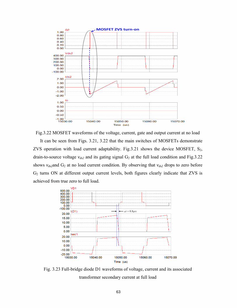
63
Fig.3.22 MOSFET waveforms of the voltage, current, gate and output current at no load
It can be seen from Figs. 3.21, 3.22 that the main switches of MOSFETs demonstrate
ZVS operation with load current adaptability. Fig.3.21 shows the device MOSFET, S2,
drain-to-source voltage vds2 and its gating signal G2 at the full load condition and Fig.3.22
shows vds2and G2 at no load current condition. By observing that vds2 drops to zero before
G2 turns ON at different output current levels, both figures clearly indicate that ZVS is
achieved from true zero to full load.
Fig. 3.23 Full-bridge diode D1 waveforms of voltage, current and its associated
transformer secondary current at full load
MOSFET ZVS turn‐on
0.8t sμ=

64
The fast reset of the circulating current of the transformer TR1 during the output
inductor freewheeling interval is illustrated in Fig.3.23. The secondary side current isec1 of
transformer TR1 drops to zero in 0.8µs with the low leakage inductance because that ZVS
of MOSFET can be achieved in the converter even while the leakage inductance is zero. It
also can be seen that full-bridge diode D1 is turned off under relatively low voltage without
severe reverse current.
Fig. 3.24 Half-bridge diode D5 waveforms of voltage and its associated transformer
secondary current at full load
Fig. 3.24 shows the waveforms of the half-bridge diode ZCS turn-on and turn-off in the
worst case of full load condition. The well-clamped voltage stress and ZCS operation of the
half-bridge diode imply that the diode voltage stress is low and the low-voltage drop diode
can be utilized to further improve the efficiency.
3.6 Performance Analysis of Hybrid Resonant and PWM Converter
As mentioned previously, this converter is able to achieve very high efficiency. In
order to obtain high efficiency, proper topology selection is critical but understand the
sources of system loss is also crucial. Many sources of loss exist in a system. First,
primary sources of loss will be considered. Some primary sources of loss are easy to
model while others may be more difficult. Primary sources of loss include the following.
• Active device conduction loss
• Diode conduction loss
ZCS turn‐onZVS turn‐off

65
• Switching loss
• Transformer core loss
• Transformer winding loss
• Inductor loss
Both active device conduction loss and diode conduction losses are fairly easy to
estimate as long as circuit operation is properly understood. Complications arise when
temperature effects are taken into account. Losses increase for MOSFETs and IGBTs at
higher temperatures and losses decrease for diodes at higher temperatures. A rough
temperature prediction can be used to improve the models. Switching loss may be difficult
to estimate accurately due to various parasitics. Package and PCB parasitic inductances
may alter switching times and switching waveforms. Both core and dc transformer
winding losses are relatively easy to estimate, although thermal effects can create
inaccuracies.
In addition to the above mentioned primary sources of loss, several parasitic sources of
loss exist. The parasitic losses include but are not limited to the following:
• Snubber loss
• Capacitor ESR loss
• Body diode conduction loss
• Skin effect
• Proximity effect
• Contact and termination loss
• Switching losses due to loss of soft switching condition
• Various losses due to temperature variation
The parasitic losses mentioned above are particularly difficult to characterize. The
losses due to skin effect and proximity effect are very difficult to model. Skin effect losses
can be prevented for the most part by utilizing copper windings which are thin enough to
ensure that sufficient surface area is available. Proximity effects are difficult to predict as
the effect is heavily dependent on how the transformer is wound. Contact and termination
losses are also difficult to model and predict. The resistance of a contact may be very
small but under high current conditions, the loss can be substantial. Switching losses due
to non-full ZVS condition is once again, difficult to predict. Partial ZVS conditions are

66
possible as shown previously. Therefore, the actual loss is very difficult to model. Finally,
the system suffers from losses due to temperature variations. It is difficult to know exact
junction temperatures of devices or core temperatures. The temperature is also dependant
on cooling and environmental factors as well. Temperature effects are partially considered
in order to form better models.
3.6.1 Main Components in This Circuit
The prototype converter has the following specifications: input voltage
380 ~ 400inV V V= ; output voltage 250 ~ 450oV V V= ; Maximum output current
_ max 15oI A= ; switching frequency 46.7sf kHz= . And the main components are tabulated
as follows.
Table 3.2: main components used in the circuit Designator MFN# Manufacturer Description
MOSFETs S1, 2 IPW60R045 Infineon
Technologies
MOSFET N-CH 650V
60A TO-247
IGBTs S3, 4 IRGP4063 International
Rectifier
IGBT PDP N-CH 600V
96A TO-247AC
Diodes D1,2,3,4 80EPF06 Vishay/
Semiconductors
DIODE FAST REC
600V 80A TO-247AC
Diodes D5,6 APT30S20 Microsemi Power
Products Group
DIODE SCHOTTKY
45A 200V TO-247
Diodes D7 APT75DQ60 Microsemi Power
Products Group
DIODE ULT FAST 75A
600V TO-247
Transformers and inductor information:
Transformer TR1 Core:
Ferrite EE80
Pri. wire #: 12
Sec. wire#: 12 Main transformer
Transformer TR2 Core:
Ferrite EE80
Pri. wire #: 12
Sec. wire#: 14 Auxiliary transformer
Inductor Lo Core:
C058195A2(High flux)
Wire#:11
(Litz wire) Output inductor
3.6.2 MOSFETs and IGBTs Conduction Loss Analysis
According datasheet, the power losses of MOSFETs and IGBTs can be calculated
[68], [69].
(a) MOSFETs Conduction Loss Analysis

67
Conduction losses in power MOSFET can be calculated using an MOSFET-
approximation with the drain source on-state resistance ( ( )DS onR ):
( )( ) ( )DS D DS on D Dv i R i i= ⋅ (3.28)
where DSv and Di are drain-source voltage and the drain current, respectively.
The typical ( )DS onR can be read from the data-sheet diagram, as shown in Fig. 3.25(a),
where DI is the MOSFET on-state current as defined by the application. Therefore, power
losses over the switching cycle gives an average value of the MOSFET conduction losses: 2
( )CM DS on DrmsP R I= ⋅ (3.29)
where DrmsI is the rms value of the MOSFET on-state current.
(a) RDS(on)vs. drain current (b) Tjvs. RDS(on)
Fig. 3.25 Reading data from data sheet
The procedure for ( )DS onR determination, shown in Fig.3.25 (b), refers to the ( )DS onR
typical values. While this procedure should be satisfying for the majority of applications,
the ( )DS onR value can be calculated by taking into account the temperature and production
variations. It can be done using following equation:
25( ) ( )max( ) (25 ) (1 )
100jT C
DS on j DS onR T R C α −= ⋅ + (3.30)
Where Tj is the junction temperature and ( )maxDS onR (25°C) is the maximum value of
( )DS onR at 25°C, which can be read from the product summary table in the data-sheet as
shown in the Fig.3.26.
( )D S o nR
DI
( ) 1D S o nR
( ) 2D S o nR
1jT 1jT

68
Fig.3.26 Reading RDS(on)max (25°C) from the data-sheet
The temperature coefficient α can be calculated in the following manner: Two sets of
values ( )1 ( )1,j DS onT R and ( )2 ( )2,j DS onT R can be read from the data sheet as shown in
Fig.3.27. These values can be used to determine α in equation (3.29).
The conduction losses of the anti-parallel diode can be estimated using a diode
approximation with a series connection of DC voltage source ( 0Dv ) representing diode on-
state zero-current voltage and a diode on-state resistance ( DR ), Dv being the voltage
across the diode and Fi the current through the diode:
0( )D F D D Fv i V R i= + ⋅ (3.31)
These parameters can be read from the diagrams in the MOSFET datasheet as shown
in Fig.3.27. In order to take the parameter variation into account, and thus to have a
conservative calculation, the 0DV value read from the diagram have to be scaled with (
max /D DtypV V ). Those exact values can be read from the datasheet tables, but for an
engineering calculation a typical safety margin value of (10%-20%) can also be used.
If the average diode current is FavI , and the rms diode current is FrmsI , the average
diode conduction losses across the switching period ( 1/sw swT f= ) are:
20CD D Fav D FrmsP V I R I= + (3.32)
Fig. 3.27 Diode resistance vs. the diode current
DD
F
VRI
=
DV
FI
0DV

69
(b) IGBTs Conduction Loss Analysis
IGBT Conduction losses can be calculated using an IGBT approximation with a series
connection of DC voltage source ( 0CEV ) representing IGBT on-state zero-current
collector-emitter voltage and a collector-emitter on-state resistance ( Cr ):
0( )CE C CE C Cv i V r i= + ⋅ (3.33)
The same approximation can be used for the anti-parallel diode, giving:
0( )D D D D Dv i V r i= + ⋅ (3.34)
These important parameters can be read directly from the IGBT Datasheet (see
Fig.3.28 (a) for the IGBT and Fig.3.28 (b) for the Diode). In order to take the parameter
variation into account, and thus to have a conservative calculation, the 0CEV and 0DV
values read from the diagram have to be scaled with ( max /CE CEtypV V ) or ( max /D DtypV V )
values. Those exact values can be read from the datasheet tables, but for an engineering
calculation a typical safety margin value of (1.1-1.2) can be used.
If the average IGBT current value is CavI , and the rms value of IGBT current is CrmsI ,
then the average losses can be expressed as: 2
0CT CE Cav C CrmsP V I r I= + (3.35)
If the average diode current is DavI , and the rms diode current is DrmsI , the average diode
conduction losses across the switching period ( 1/sw swT f= ) are:
20CD D Dav D DrmsP V I r I= + (3.36)
(a) VCE0 vs. rc (b) VD0 vs. rD
Fig. 3.28 Reading data from datasheet
CEVcI
0CEV
CEC
C
VrI
=
DD
D
VrI
=
DVDI
0DV

70
3.6.3 Diode Conduction Loss Analysis
In addition to MOSFETs and IGBTs conduction losses, there are diode conduction
losses on the secondary side.
When the forward current maxI is lower than 3 FavI⋅ , similar to the anti-parallel diode
loss calculation of the active device, the diode conduction loss can be calculated as
2CD F Fav ak FrmsP V I R I= + (3.37)
where FV is Diode fixed voltage drop under zero current condition; FavI is average
forward current in the diode; FrmsI is RMS forward current in the diode; akR Diode on-
drop resistance.
When the forward current maxI is higher than 3 FavI⋅ , diode on-drop resistance, akR ,
becomes very pessimistic. The diode conduction loss can be calculated as
( )CD FM M FavP V I I= ⋅ (3.38)
where ( )FM MV I is the FMV value when FM MI I= ; FavI is average forward current in the
diode.
3.6.4 MOSFET and IGBT Switching Loss Analysis
Switching loss is also a common source of loss in switching converters. Loss must be
calculated for both turn-on and turn-off conditions to find the total switching loss. During
commutation, voltage and current can be high as each crosses over the other. The
switching energy loss, Esw, is the integration of the V Ii product during the commutation
state.
_ _
( ) ( ) ( ) ( ) ( ) ( )i on i off
sw sw sw on off sw sw sw swswitching time t t
E v t i t dt E E v t i t dt v t i t dt= = + = +∫ ∫ ∫ (3.39)
where _i ont is used for the unambiguous definition of integration limits for the
determination turn-on switching losses; _i offt is used for the unambiguous definition of
integration limits for the determination turn-off switching losses; onE is turn-on energy
loss; offE is turn-off energy loss.

71
If soft switching is achieved, the switching loss for that particular device can be
reduced significantly. Under ZVS or Zero Current Switching (ZCS) conditions, the
switching loss can be considered zero.
Then the average switching loss can be expressed as
swsw sw sw
sw
EP f ET
= = (3.40)
The switching times are defined as follows:
( )d ont is turn-on delay time; ( )d offt is turn-off delay time; rt is rise time; ft is fall time; and
( )on d on rt t t= + is turn-on time; ( )off d off ft t t= + is turn-off time.
The values for toff and ton should ideally be measured. Sometimes, measurement may
be difficult. Typically, the device manufacturer will provide some typical values for toff
and ton and values for Eoff and Eon maybe provided as well. Unfortunately, the values for
toff, ton, and Eoff, and Eon are dependent on many factors including temperature, current, gate
resistor, gate voltage, load type (resistive or inductive), etc. Typically, the values provided
by the manufacturer will not match exactly. If the test conditions are very similar, then the
manufacturer’s datasheet may provide a reasonable estimate. The manufacturer does
provide a plot of switching energy vs. load current based on inductive switching.
Fig.3.29 shows MOSFET typical characteristic of gate-source voltage VGS, drain-
source voltage VDS and drain-source current IDS, and its definition of switching times and
switching energies.
Fig. 3.29 Definitions of MOSFET switching times and energies
Eon is turn-on switching energy with diode, which is the integral of the product of drain
current and drain-source voltage over the interval ( _i ont ) from when the drain current
starts to rise to when the voltage falls to zero in order to exclude any losses. Eoff is Turn-
off Switching Energy, which is the integral of the product of drain current and drain-
10%DSV GSVrt ft
( )d offt
10% 10% 10%
10% 10%
t
DSI
( )d ont
_i o f ft_i o nt( )
o n
o n
PE ( )
o f f
o ff
P
E
ont offt

72
source voltage over the interval ( _i offt ) starting from when the gate-source voltage drops
below 90% to when the drain current reaches zero.
In our circuit, MOSFETs operate at ZVS conditions, so there is no turn-on loss, which
means 0onE = .
Switching energy can be scaled directly for variation between application voltage and
the datasheet switching energy test voltage. So if the datasheet tests were done at 330
Volts for example, and the application is at 400 Volts, simply multiply the datasheet
switching energy values by the ratio 400/330 to scale.
MOSFET switching loss may be estimated by calculating the area underneath the VDS
and ID waveforms and multiplying by the switching frequency and switching times.
The equations [67] below can be used as crude estimates of the area underneath the
VDS and ID waveforms or the switching energy.
_12o n D S D S i o nE V I t= (3.41)
_12o f f D S D S i o f fE V I t= (3.42)
( )_ _lo s s sw M O S F E T o n o ff sP E E f= + (3.43)
Fig.3.30 shows IGBT typical characteristic of gate-emitter voltage VGE, collector-
emitter voltage VCE and collector current Ic, and its definition of switching times and
switching energies.
Fig. 3.30 Definitions of IGBT switching times and energies
Eon is Turn-On Switching Loss, which is the amount of total energy loss, including the
loss from the diode reverse recovery, measured from the point where the collector current
begins to flow to the point where the collector-emitter voltage completely falls to zero in
10%
CEV
GEV
rt ft( )d offt
10%
10%
10%
t
CI
( )d ontont offt
( )o n
o n
PE
0.1 cI( )
o ff
o f f
P
E
10%
i o nt i o f ft

73
order to exclude any conduction loss. Eoff is turn-off Switching Loss, which is the amount
of total energy measured from the point where the collector-emitter voltage begins to rise
from zero to the point where the collector current falls completely to zero.
In our circuit, IGBTs operate at ZCS conditions, so there is no turn-off loss, which
means 0offE = .
Similarly, IGBT switching loss may be estimated by calculating the area underneath
the VCE and IC waveforms and multiplying by the switching frequency and switching
times.
The equations [67] below can be used as crude estimates of the area underneath the
VCE and IC waveforms or the switching energy.
_12o n C E C i o nE V I t= (3.44)
_12o ff C E C i o ffE V I t= (3.45)
( )_ _lo ss sw IG B T o n o ff sP E E f= + (3.46)
Time and loss components which cannot be unambiguously described by the switching
time definitions can be taken in consideration practically (e.g. the tail current characteristic
for the IGBT).
3.6.5 Transformer Core Loss Analysis
Magnetic components such as inductors and transformers typically have core loss
associated with them. The first step is to find the applied voltage-seconds. The voltage
seconds is dependent on the duty cycle.
Fig.3.31 An arbitrary voltage waveforms
area λ( )v t
t1t 2t

74
An arbitrary periodic transformer primary voltage waveform ( )v t is illustrated in
Fig.3.31. The volt-seconds applied during the positive potion of the waveform is denoted
λ :
( )2
1
t
tv t d tλ = ∫ (3.47)
These volt-seconds, or flux-linkages, cause the flux density to change from its
negative peak to its positive peak value. Hence, from Faraday’ law, the peak value ( BΔ )
of the ac component of the flux density is
12 e
Bn Aλ
Δ = (3.48)
1n = Number of Primary Transformer Turns
eA = Effective Core Area of Transformer
Some key trends may be noticed from equations (3.46), (3.47):
• Increases in input voltage increases peak flux density.
• Increases in switching frequency decreases peak flux density.
• Increasing the number of primary turns decreases peak flux density
The peak flux density is dependent on applied voltage-seconds, primary transformer
turns ratio, and effective core area. Since peak flux density is directly related to core loss,
one can easily see how to modify the transformer design to reduce core loss. Typically, the
input voltage cannot be changed but switching frequency can be increased to reduce
applied voltage-seconds. Unfortunately, increases in switching frequency may lead to
increased switching loss. Primary turns ratio can easily be increased as long as there is
sufficient space, but resistance and losses will increase due to increased winding lengths.
Larger cores may be used to increase effective core area but size and cost of the
transformer will increase.
Once the ac peak flux density is known, the core loss can be estimated. The following
equation for core loss calculation offers a close approximation.
dcL BafP = (3.49)

75
where LP is Power loss in 3/m W c m ; B is Peak flux density in kG; f is frequency in
kHz. In our circuit, a ferrite EE80 core is used and the loss parameters can be looked up in
the table as follows provided by Magnetics Inc.
Table 3.3: factors applied to the above formula (3.49)
Material type Frequency range a c d
R Material
100f kHz<
100 500kHz f kHz≤ <
500f kHz≥
0.074
0.036
0.014
1.43
1.64
1.84
2.85
2.68
2.28
P Material
100f kHz<
100 500kHz f kHz≤ <
500f kHz≥
0.158
0.0434
7.36×10⁻⁷
1.36
1.63
3.47
2.86
2.62
2.54
F Material
10f kHz<
10 100kHz f kHz≤ <
100 500kHz f kHz≤ <
500f kHz≥
0.790
0.0717
0.0573
0.0126
1.06
1.72
1.66
1.88
2.85
2.66
2.68
2.29
J Material 20f kHz≤
20f kHz>
0.245
0.00458
1.39
2.42
2.50
2.50
W Material 20f kHz≤
20f kHz>
0.300
0.00382
1.26
2.32
2.60
2.62
H Material 20f kHz≤
20f kHz>
0.148
0.135
1.50
1.62
2.25
2.15
Then we can estimate approximately the total core loss as follows. c d
fe L c e mP P V a f B A l= = (3.50)
eA = Effective Core Area of Transformer (cm2)
ml =Magnetic path length (cm)
Like many other devices components, core loss is heavily dependent on temperature.
The transformer core temperature coefficient varies and may be negative or positive over
different temperature ranges. At low temperatures, the core loss is typically high. The core

76
loss decreases as temperature increases. At a certain point, there is an inflection point and
the core loss increases again as temperature increases. The temperature range that
minimizes the core loss is dependent on the material of the core. The core loss variation
due to temperature is also dependent on frequency and peak flux density which core loss
estimations even further.
3.6.6 Transformer Copper Loss Analysis
Transformers also have copper loses in addition to core losses. The copper losses are
increased further due to skin and proximity effects if the transformer is not properly
designed. Copper loss simply due to current is easy to estimate, but the loss estimation
becomes substantially more difficult when other factors such as skin effect and proximity
effects are considered. Ignoring the copper losses due to skin and proximity effects, the
total copper loss can be expressed in the form
( ) 2 21 tot
cuA u
MLT n IP
W Kρ
= (3.51)
Combining equations (47) and (49), it yields
( ) 22 2
2
14
totcu
u A e
MLTIPK W A B
ρλ ⎛ ⎞⎛ ⎞ ⎛ ⎞= ⎜ ⎟⎜ ⎟ ⎜ ⎟⎝ ⎠⎝ ⎠ ⎝ ⎠
(3.52)
1 1
kj
tot jj
nI I
n=
=∑ , is the sum of the rms winding currents, referred to the primary winding.
=ρ Resistivity of copper = 61.724 10 cm−× Ω ⋅ @25°C and 62.3 10 cm−× Ω ⋅ @100°C.
MLT = Mean length per turn.
n1 = Number of primary winding turns.
WA = Bobbin winding area.
Ku = Winding fill factor, is the fraction of the core window area that is filled with copper.
The dc resistance of a transformer winding can be calculated with the following
equation.
c
lRA
ρ= (3.53)
=l Length of winding
cA = Cross-sectional area of copper

77
Under given core type and size, winding turns and the wire that is used, we can look
up the data we need from the core data and wire gauge data provided by the manufacturer.
The DC resistance of primary and secondary windings can also be obtained as follows.
The DC winding resistance for the primary side is:
( )( )1 _ #pri pri A W GR n M L T R= (3.54)
The DC winding resistance for the secondary side is
( ) ( )sec 2 sec_ #A W GR n M L T R= (3.55)
If the primary and secondary currents are known, then the total copper loss is given 2 2
sec seccu pri priP I R I R= + (3.56)
n1 = Number of primary winding turns.
n2 = Number of secondary winding turns.
_ #pri AWGR is the primary wire resistance in 610 / cm− Ω .
sec_ #AWGR is the secondary wire resistance in 610 / cm− Ω .
Losses such as core loss, contact loss, and copper loss, create heat and raise the
temperature of the transformer windings. This in turn causes copper losses to increase.
The increase in temperature also makes copper more susceptible to skin effect. Skin effect
can greatly increase the effective resistance of a high frequency transformer winding and,
therefore, creating additional losses. Even if wire is selected such that skin depth matches
the copper thickness, the current density varies throughout the depth. Therefore, greater
amounts of current will flow at the surface and less current at the center of the conductor.
The conductor is still not fully utilized and therefore, the effective resistance will increase.
3.6.7 Inductor Loss
Inductors dissipate power in the core and in the windings. Though determining these
losses with precision can require complex measurements, an easier alternative exists.
Inductor losses may be estimated using readily available data from core and inductor
suppliers along with the relevant power supply application parameters.
The power loss of an inductor is defined by the basic formula:
_loss inductor core dcr acrP P P P= + + (3.57)

78
The calculated and/or measured core loss, coreP , is often directly provided by the
inductor supplier. If not, a formula can be used to calculate the core loss. First of all, the
ac peak flux density (B in Telsa) needs to be obtained and it is given as follows.
I
e
NBlμ
= (3.58)
where
N=number of turns
le=effective magnetic length
Measuring core loss and getting repeatable results can be a tedious task depending on the
test frequency. A general form of the core loss formula for ferrite cores is:
( ) x ycore eP mW af B V= (3.59)
where:
a= Constant for core material
f = Frequency in kHz
B = Peak Flux Density in kGauss
x = Frequency exponent
y = Flux Density exponent
Ve= Effective core volume (cm3)
The core loss can be calculated by entering the ‘a’ coefficient and the frequency and
flux density exponents, which are unique to each core material. For example, in this
circuit, high flux core is used and B in the formula is in Tesla and the core loss density
curves can be obtained from the supplier (Magnetics) as shown in Fig.3.32.
Fig. 3.32 Core loss density curves of the output inductor

79
The wire loss ( dcrP ) caused by dc resistance is easy to calculate. It is defined by this
basic formula: 2
dcr rms dcP I R= (3.60)
where:
Irms= Therms value of the peak current applied to the inductor
Rdc= The dc resistance of the inductor
The wire loss ( acrP ) caused by ac resistance is more difficult to calculate since ac
winding resistance values are not always readily available from magnetics vendors. Pacr is
defined by the following formula: 2
acr rms acP I R= (3.61)
where:
Irms= Therms value of the peak-peak ripple current applied to the inductor
Rac= The ac resistance of the inductor
In many cases Pacr is a small percentage of the overall inductor power loss, thus, the
power loss of an inductor is defined by the simple formula
_loss inductor core dcrP P P= + (3.62)
3.6.8 Other Losses
Calculating power loss for the snubber is rather difficult since it can be dependent on
switching characteristics. When full ZVS condition is obtained, the snubber loss decreases
due to less severe perturbations. Hard switching conditions create heavy voltage spikes
and ripples, which must be damped by the snubber.
Many other parasitic losses exist within the system. For example, capacitor ESR is a
concern, particularly for high current systems. Capacitors are important for maintaining
waveform quality and reducing voltage spikes and ripples. These capacitors may have to
supply and draw large amounts of current. The capacitor ESR losses can become
significant when the current is large. Paralleling additional capacitors can help reduce
losses due to capacitor ESR since RMS current through individual capacitors is reduced.
Another source of loss, which is difficult to be estimated is parasitic inductance.
Parasitic inductance can cause excessive voltage spikes during switching. Switching
waveforms affected will see larger losses in addition to higher voltage stress. Higher

80
voltage stress may lead to device failure. If higher voltage rating devices are used,
typically conduction loss of the device increases since the voltage rating has increased.
Termination is another major parasitic loss, especially for high current situation. Each
mechanical connection made introduces termination losses. Mechanical connections do
not have perfect contact and a small resistance exists between the two contacts. Ideally,
mechanical contacts should be eliminated where possible and one piece of copper should
be used for connection. The mechanical contacts may have a small resistance but the loss
can become very high due to the large currents of high current systems. The loss would be
simple to calculate with the conduction loss equation, but the resistance is difficult to
predict since the resistance is due to the physical construction. Under high current
conditions, the terminals can get hot due to the power loss. The higher temperature
increases the resistance of copper, further increasing parasitic losses. In addition to
mechanical contact resistance, the resistance increases further if two different materials are
used for contacts.
Skin effect and proximity effect can also create significant amounts of loss. Skin effect
raises the effective resistance of the transformer winding. Since large currents are flowing
through the transformer, an increase in resistance can create large amounts of loss.
3.6.9 Efficiency Estimation
Based on the loss estimations above, the efficiency can be estimated. Once again, the
temperature and other factors have a significant effect on system efficiency. For this
estimation, the following conditions will be assumed.
Table 3.4: Efficiency estimation conditions
Input Voltage 380~400V
Output Voltage 250~450V
Maximum Output Power 6.6kW
Switching frequency 46.7kHz
The total power loss can be calculated shown in Fig.3.33 (a) and the efficiency of the
system can be estimated shown in Fig.3.33 (b).

81
(a) Calculated total loss vs. Po (b) Calculated efficiency vs. Po
Fig.3.33 Calculated total loss and efficiency vs. output power
As an example, specifically the estimated power losses at 3.4-kW rated output power
with two different output voltage levels are listed in the Fig. 3.34. It indicates that the
output diodes and IGBTs are the dominant sources of the power losses under full-load
condition.
Fig. 3.34 Estimated power losses at 3.4 kW rated output power with two different output
voltage levels
3.7 Topology Variations
Fig.3.35 demonstrates several ZVZCS full-bridge combining resonant half-bridge
converters with different rectifier configurations, which share the common feature that the
full-bridge converter changes to half-bridge converter and keeps transferring energy from
the input to the output during the freewheeling interval of the output inductor. It is worth to
0 0.5 1 1.5 2 2.5 3 3.5 4 4.5 5 5.5 6 6.5 7
20
40
60
80
100
120
140
160
Po (kW)
Tota
l los
s (W
)
0 0.5 1 1.5 2 2.5 3 3.5 4 4.5 5 5.5 6 6.5 70.8
0.82
0.84
0.86
0.88
0.9
0.92
0.94
0.96
0.98
1
Po (kW)
Effi
cien
cy
12.59.5
16.6
2.3 2.5
14.4
8.0 8.0
24.0
5.0
11.39.2
14.4
20.7
0
5
10
15
20
25
30
IGBTs MOSFETs Maintransformer
Auxiliarytrans.
Outputinductor
Outputdiodes
Others
Po=3400W;Vin=390V; Vo=385VPo=3400W;Vin=390V;Vo=280V
Pow
er lo
ss (W
)
12.59.5
16.6
2.3 2.5
14.4
8.0 8.0
24.0
5.0
11.39.2
14.4
20.7
0
5
10
15
20
25
30
IGBTs MOSFETs Maintransformer
Auxiliarytrans.
Outputinductor
Outputdiodes
Others
Po=3400W;Vin=390V; Vo=385VPo=3400W;Vin=390V;Vo=280V
Pow
er lo
ss (W
)

82
note that the resonant converter can be half-bridge or full-bridge or other high efficiency
parallel or series or multi-element resonant converters, and that the switches leg
configuration can be two-level or three-level with IGBT or MOSFET or hybrid devices.
(a) with two central tapped rectifiers
(b) with full-bridge and central tapped rectifiers
(c) with full-bridge and central tapped synchronous rectifiers
Fig.3.35 Several variations hybrid resonant and PWM converters
1S
2S
3S
4S
1D 2D 3D
1C
2C
oL
oRoC
inV TR1 TR1
4D
5D
TR1
1S
2S
3S
4S
1D
2D 4D
3D
inV
1C
2C
oL
oRoC
TR2
4D5D 6D
TR1
1S
2S
3S
4S
1D
2D 4D
3D
inV
1C
2C
oL
oRoC
TR2
5D
5S6S
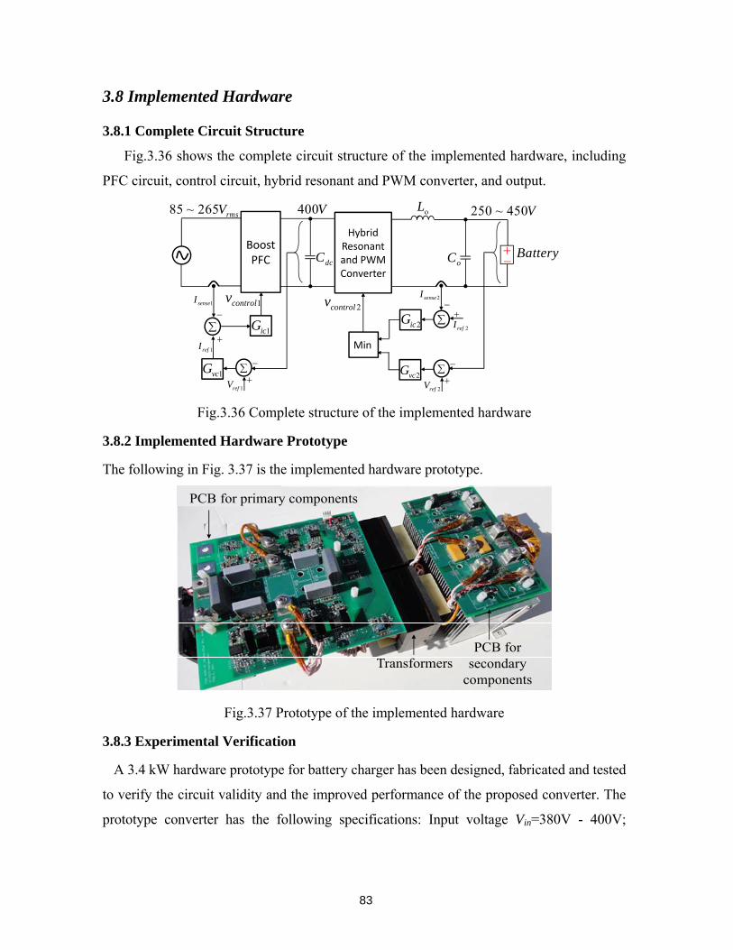
83
3.8 Implemented Hardware
3.8.1 Complete Circuit Structure
Fig.3.36 shows the complete circuit structure of the implemented hardware, including
PFC circuit, control circuit, hybrid resonant and PWM converter, and output.
Fig.3.36 Complete structure of the implemented hardware
3.8.2 Implemented Hardware Prototype
The following in Fig. 3.37 is the implemented hardware prototype.
Fig.3.37 Prototype of the implemented hardware
3.8.3 Experimental Verification
A 3.4 kW hardware prototype for battery charger has been designed, fabricated and tested
to verify the circuit validity and the improved performance of the proposed converter. The
prototype converter has the following specifications: Input voltage Vin=380V - 400V;
oL
BatteryoC
Hybrid Resonant and PWM Converter
Min
2icG
2vcG
+
+
−
−
2refI
2refV
∑
∑
2controlv
Boost PFC
250 ~ 450V85 ~ 265 rmsV
+−dcC
−
1vcG+
−
1refV∑
1icG∑+
400V
1refI
1senseI 2senseI1controlv
PCB for primary components
PCB for secondary
components Transformers

84
Output voltage Vo=250V – 450V; Maximum output current Io-max =15A; Switching
frequency fs=46.7kHz.
Fig. 3.38 Power circuit and the parameters of the prototype
Fig.3.38 shows the power circuit and the parameters of the prototype with the part
numbers of the components used. All power semiconductor devices including MOSFETs
(S1 and S2), IGBTs (S3 and S4) and diodes (D1~D7) are mounted on the heat-sink with the
same TO247 package. The transformer TR1 is designed with tightly coupling and without
airgap in the Ferrite EE80 core (magnetizing inductance Lm1=7.1mH, leakage inductance
Llk1=3.9µH), and the transformer TR2 with loosely coupling and airgap in the core
(magnetizing inductance Lm2=566µH, leakage inductance Llk2=35µH).
ZCS operation of the main device IGBT is verified by the experimental waveforms of the
IGBT (S4) voltage Vce4, device current ic4, and gate voltage G4, shown in Fig.3.39. Before
the gate is turned off, the device current ic4 is nearly zero, so the IGBT operates at zero-
current switching condition in the worst case of the maximum output power.
Fig.3.39 IGBT ZCS experiment waveforms of device voltage, current, and its gate.
TR1 TR2
oV−
+
1S
2S
3S
4S
1D
2D4D
3D 5D
6D7D
3C
1C
2C
oL
oRoC
inV
1
1
7.13.9
m
k
L mHL Hμ
==
2
2
56635
m
k
L HL H
μμ
==
3 ,4 :30 60
SH G T G N
2934
1,2 : 60 045S IP W R
4013
0.33 Fμ
10 Fμ
10 Fμ20 Fμ
0.2mH
1~ 4 :80 06D
E P F5 , 6 :
8 0 1 5 0D
C P Q7 :
75 60D
A P T D Q
C3
G4 (10V/div)
Vce4 (200V/div)
ic4 (10A/div)
t (2µs/div)
ZCS
C3C3
G4 (10V/div)
Vce4 (200V/div)
ic4 (10A/div)
t (2µs/div)
ZCS

85
Fig. 3.40 shows the experimental verification of the MOSFETs main switches ZVS
operation with load current adaptability. Fig.3.40 (a) shows the device MOSFET, S2, drain-
to-source voltage vds2 and its gating signal G2 at no load condition, and Fig.3.40 (b) shows
vds2and G2 at the full load current condition (8.8A). The gate voltage is 15V for turn on and
-5V for turn off. By observing that vds2 drops to zero before G2 turns ON at different output
current levels, both figures clearly indicate that ZVS is achieved from zero to full load.
The fast reset of the circulating current of the transformer TR1 during the output inductor
freewheeling interval is illustrated in Fig3.41. The secondary side current isec1 of
transformer TR1 drops to zero in 0.7µs with the low leakage inductance because that ZVS
of MOSFET can be achieved in the proposed converter even while the leakage inductance
is zero. It also can be seen that full-bridge diode D1 is turned off under relatively low
voltage without severe reverse current.
(a)zero load(b) full load Io= 8.8A
Fig. 3.40 MOSFET ZVS load adaptability experiments with different load conditions
Fig.3.41 Full-bridge diode D1 waveforms of voltage, current and its associated
transformer secondary current.
Fig. 3.42 shows tested waveforms of the half-bridge diode ZCS turn-on and turn-off in
the worst case of the maximum output current. The well-clamped voltage stress and ZCS
G2 (10V/div)
Vds2 (250V/div)
io (5A/div)0
t (2µs/div)
ZVSG2 (10V/div)
Vds2 (250V/div)
io (5A/div)
8.8A
t (2µs/div)
ZVS
C3C3
VD1 (200V/div)
iD1 (10A/div)
t (5µs/div)isec1 (10A/div)
Δt=0.7 µs

86
operation of the half-bridge diode imply that the diode voltage stress is low and the low-
voltage drop diode can be utilized to further improve the efficiency.
Fig. 3.42 Half-bridge diode D5 experimental waveforms of voltage and its associated
transformer secondary current.
The measured efficiency at different loads under the condition of 46.7 kHz switching
frequency, 390 V input, 385 V and 280 V output is given in Fig. 3.43. It can be seen that
high efficiency over wide load current and output voltage range is achieved. The efficiency
with load range from 20% to 100% maintains 96% or higher, and the maximum efficiency
achieves 98% under the conditions of 385V output voltage and 3.4 kW output power. The
efficiency is higher with a higher output voltage because that the conduction losses of the
active switches and output diodes are reduced with the lower current stresses.
Fig. 3.43 Experimental results of efficiency as a function of the output power.
3.9 Summary
A novel hybrid resonant and PWM converter combining resonant half-bridge and phase
shifted full-bridge topology has been proposed to achieve high efficiency and true full soft-
ZCS turn-onZCS turn-off
VD5 (100V/div)
isec2 (5A/div)
t (5µs/div)
86%
88%
90%
92%
94%
96%
98%
100%
0 500 1000 1500 2000 2500 3000 3500
Vo = 385V
Vo = 280V
Output power (W)
Effic
ienc
y
@ f = 46.7 kHz, Vin = 390V

87
switching range, which is also verified by a 3.4 kW hardware prototype. Table 3.2
summarizes the factors that determine the performances of the three converters.
Table 3.5: phase-shifted full bridge, LLC and Proposed Converters
Control
method
ZVS
range
Circulating
current
Constant Current
and Voltage
Output diode
voltage stress
PS FB Fixed
frequency
Limited
range High Yes High
LLC Variable
frequency
Full
range Low No Low
Proposed
converter
Fixed
frequency
Full
range Low Yes Low
NOTE: PS HB represents phase-shifted full bridge converter; LLC represents LLC
converter; Llk1 is Leakage inductance of the transformer in PS FB; Lm2 is Magnetizing
inductance the transformer in LLC; Lf is Output inductor; Ro is output load.
From Table 3.5 and Fig.3.44, it can be seen that the proposed hybrid converter can
realize the full range ZVS by designing suitable magnetizing inductanceLm2used in LLC
and the leakage inductance Llk1 of the transformer used in phase-shifted full bridge called
main transformer TR1 is independent of the ZVS. Since Llk1 is no longer related to the
ZVS, it can be minimized to reduce the duty cycle loss and circulating current.
Fig.3.44 Key waveforms and formulaof the proposed hybrid converter
The distinctive features of the proposed circuit are summarized as follows:
21
1in lk
nslope V Ln
= −
1privrectv
1prii0
/ 2sT
( )/ 2slossD TΔ resetTZC ST
t
1 inn V
inV
2 inn V
t0
( ) ( )1 1/in o oslope n V V L n= −1 2
11
/in lkn nslope V L
n⎛ ⎞−
= ⎜ ⎟⎝ ⎠

88
1) With the parallel LLC resonant half-bridge configuration, zero-voltage switching of
MOSFETs in the leading-leg can be ensured from true zero to full load, and thus, the
super-junction MOSFET with slow reverse recovery body diode can be reliably used.
2) IGBTs in the lagging-leg work at zero-current switching with minimum circulating
conduction loss because the parallel secondary-side DC voltage source effectively reset
the circulating current, therefore, the turn-off loss and the conduction loss of the IGBTs
are significantly reduced.
3) Duty cycle loss is negligible since the leakage inductance of the main transformer can
be minimized without losing ZVS operation, thus, the current stresses through the
primary-side semiconductors are minimized by the optimized turns ratio of the main
transformer.
4) The topology is suitable for wide-range output voltage or current source applications
because of the buck-type configuration with the simple phase-shift pulse width
modulation, and thus, it is a good candidate for the electrical vehicle battery charger.

89
CH4: Improved Hybrid Resonant and PWM Converter
4.1 Issues in Previous Hybrid Resonant and PWM Converter
The hybrid LLC resonant and phase-shifted full bridge PWM converter described in
CH3 is repeated here as shown in Fig.4.1 (a) and the key operation waveforms is shown in
Fig. 4.1(b).
(a)The circuit configuration (b) Key operation waveforms
Fig. 4.1 Hybrid resonant and PWM converter in CH3
Fig.4.3 is the topological mode [t0, t1] repeated here in which the blue regular indicates
the effective duty cycle in the operation waveforms as shown in Fig.4.3 (b).
(a)The circuit mode topology (b) Key operation waveforms
Fig. 4.2 Mode [t0, t1] for the hybrid resonant and PWM converter
From Fig.4.2, it can be concluded that if the effective duty cycle is large for the main
transformer, the energy stored in capacitor C1 or C2 charged by LLC converter has no chance
to be transferred to the output, which means the utilization efficiency of the auxiliary
1prii 2prii
rectv oV−
+
−
+
1S
2S
3S
4S
1D
2D4D
3D 5D
6D
7D
3C
1C
2C
oL
oRoC
m2Llk1L lk2L
inV1TR
2TR
1SC
2SC
2Lmi1dsv−+
1prii
2prii
rectvoV
t
t
t
t
t
0
0
0
2S 1S 2S
3S 4S 3S
GSv
GSv
0t 1t 2t 3t 4t 5t 6t
2mLi
t1dsv0
1prii 2prii
rectv ov−
+
−
+
1S
2S
3S
4S
1D
2D4D
3D 5D
6D
7D
3C
1C
2C
oL
oRoC
m2Llk1L lk2LinV
1TR 2TR
[ ]0 1,t t1SC
2SC
1prii
2prii
rectvov
t
t
t
t
t
0
0
0
2S 1S 2S
3S 4S 3S
GSv
GSv
0t 1t 2t 3t 4t 5t 6t
2mi
t1dsv0

90
transformer is very low in this case. When it is high power application, it requires the duty
cycle large, then the auxiliary transformer TR2 charges the capacitor C2 or C1 while the main
transformer TR1 is transferring the energy to the output load. So the issue is how to get the
auxiliary transformer TR2 utilized more efficiently?
4.2 The Improved Hybrid Resonant and PWM Converter
Fig.4.3 is a solution for the previous issues, in which the output of the LLC resonant
converter is in series with the output load, theoretically transferring energy to the output all
the time.
Fig. 4.3 The improved circuit configuration
4.2.1 Operational Principles
Fig.4.4 (a) show the circuit diagram of the improved Hybrid Resonant and PWM
Converter which composed of two parts similar to the previous hybrid resonant and PWM
converter: 1) the resonant half-bridge circuit including two MOSFETs S1 and S2, loosely
coupled transformer TR2, resonant capacitor C3, and the secondary rectifier D5, D6, and C1,
C2; 2) the phase shifted full-bridge circuit including two MOSFETs S1 and S2 as leading-
lag, two IGBTs as lagging-leg, tightly coupled transformer TR1, the secondary rectifier
D1~4, and the LC output filter. The topology operating principle can be explained by the
gating sequence and associated key voltage and current waveforms shown in Fig.4.4 (b).
Where Cs1, Cs2 are the equivalent capacitance of the MOSFETs S1, S2, respectively; vrect is
voltage of the output inductor left-side point referred to the output ground; Vo is the output
voltage; ipri1 and ipri2 are the primary current of the transformer TR1 and TR2 respectively;
iLm2is the magnetizing current of the transformer TR2; and the vds1 is the device S1 drain-to-
source voltage.
oV
rectV
t0
TR1TR2
1S
2S
3S
4S
1D
2D
5D
6D
3C
4D
3D
1C
2C
oL
oRoC
inV
rectv
−
+
oV−
+
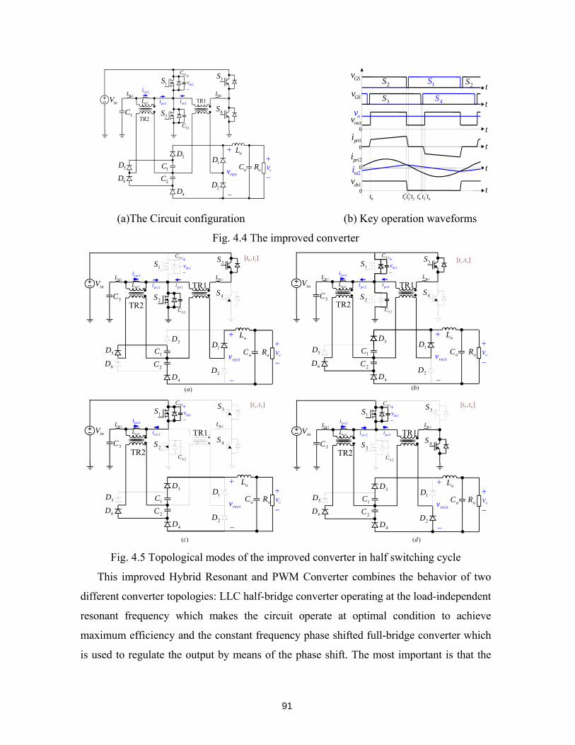
91
(a)The Circuit configuration (b) Key operation waveforms
Fig. 4.4 The improved converter
Fig. 4.5 Topological modes of the improved converter in half switching cycle
This improved Hybrid Resonant and PWM Converter combines the behavior of two
different converter topologies: LLC half-bridge converter operating at the load-independent
resonant frequency which makes the circuit operate at optimal condition to achieve
maximum efficiency and the constant frequency phase shifted full-bridge converter which
is used to regulate the output by means of the phase shift. The most important is that the
TR1
TR2
1S
2S
3S
4S
1D
2D
5D
6D
3C
4D
3D
1C
2C
oL
oRoC
inV
rectv
−
+
−
+
1prii2priim2Llk1Llk2L
1SC
2SC
1dsv−
+
oV
2Lmi
1prii
2prii
rectv ov
t
t
t
t
t
0
0
0
2S 1S 2S
3S 4S
GSv
GSv
0t 1t 2t 3t 4t
2mi
t1dsv0
5t 6t
TR1
TR2
1S
2S
3S
4S
1D
2D
5D
6D
3C
4D
3D
1C
2C
oL
oRoC
inV
rectv
−
+
−
+
1prii2priim2Llk1Llk2L
1SC
2SC
1dsv−
+
oV
2Lmi
TR1
TR2
1S
2S
3S
4S
1D
2D
5D
6D
3C
4D
3D
1C
2C
oL
oRoC
inV
rectv
−
+
−
+
1prii2priim2Llk1Llk2L
1SC
2SC
1dsv−
+
oV
2Lmi
TR1
TR2
1S
2S
3S
4S
1D
2D
5D
6D
3C
4D
3D
1C
2C
oL
oRoC
inV
rectv
−
+
−
+
2priim2Llk1Llk2L
1SC
2SC
1dsv−
+
oV
2Lmi
0 1[ , ]t t1 3[ , ]t t
3 5[ , ]t t
( )a ( )b
( )c
TR1
TR2
1S
2S
3S
4S
1D
2D
5D
6D
3C
4D
3D
1C
2C
oL
oRoC
inV
rectv
−
+
−
+
1prii2priim2Llk1Llk2L
1SC
2SC
1dsv−
+
oV
2Lmi
5 6[ , ]t t
( )d

92
output of the LLC half bridge is in series with the output of the converter, thus the auxiliary
transformer TR2 can get improved greatly. Whatever the duty cycle is, the energy stored in
the capacitor C2 or C1 through the auxiliary transformer TR2 can be transferred to the
output load. There are six distinct operation modes for this topology in the PWM half
cycle, as shown as Fig.4.5.
Mode [t0, t1]: At t0, the secondary current of transformer TR1 reaches at the reflected
output inductor current. Switches S3 and S2 remain on. Suppose the leakage inductance of
the main transformer is zero, that is 1 0lkL = . Thus, the equivalent circuit at this interval is
shown in Fig.4.6, as well as the key waveforms.
Fig.4.6 (a), (b) The equivalent circuit for Mode [t0, t1];(c) The key waveforms
According to half bridge LLC characteristics, the sec2v shown in from Fig.4.6 (b) can be
expressed as
sec 2 2 1 212 in c cv n V V V⎛ ⎞= ⋅ = =⎜ ⎟
⎝ ⎠ (4.1)
where n2 is the secondary-to-primary turns ratio of TR2.
Clearly from Fig.4.6 (a), the reflected input voltage applies to the left-side of the output
inductor called the rectified voltage, vrect, which can be expressed as
1 212rect in inv n V n V= ⋅ + (4.2)
where n1 is the secondary-to-primary turns ratio of TR1. vrect is the rectified voltage and Vin
is input voltage shown in Fig.4.4. The primary current of the main transformer reaches the
reflected current of the output inductor, Lo, and increases with the slope as
1prii
2prii
rectv ov
t
t
t
t
t
0
0
0
2S 1S 2S
3S 4S
GSv
GSv
0t 1t 2t 3t 4t
2mi
t1dsv0
5t 6t
1prii
2prii
rectv ov−
+
3C 1C
oLoRoC
m2L
lk2L
inV
2TR
11: n
1TR
21: n
2Lmi sec2v−
+
xi
(a)
(b)
2C
2cv −+−
+

93
( )11 2 1
1 /2
priin in o o
din V n V V L n
dt⎛ ⎞= + −⎜ ⎟⎝ ⎠
(4.3)
Suppose output capacitors, C1 and C2, are large enough. Thus, the primary side of
Fig.4.6 (b) can be simplified as Fig.4.7 as follows.
Fig.4.7 The simplified circuit for the primary side of Fig.4.6 (b)
The magnetizing current iLm2can be simplified as a triangle wave with a constant slope
as follows.
2 / 2Lm in
m
di Vdt L
=
(4.4)
where n2 are the secondary-to-primary turns ratio TR2. Thus,
( ) ( )2 2 0 0/ 2 ( )in
Lm Lmm
Vi t i t t tL
⎡ ⎤= + −⎢ ⎥⎣ ⎦
(4.5)
2 0( )Lmi t is the current flowing the resonant capacitor Lm2 at t0.
Since the circuit operates at resonant frequency, where the voltage gain is constant, a
little bit higher than unity, which is independent of load and ratio of m ( /m lkm L L= , mL is
the transformer magnetizing inductance and lkL is the transformer leakage inductance),
Lm2 can be relatively large as needed. Suppose output capacitors, C1 and C2, are large
enough. Then the secondary side of Fig.4.6 (b) can be simplified as Fig.4.8 as follows.
Fig.4.8 The simplified circuit for the secondary side of Fig.4.6 (b)
Suppose the voltage across the resonant capacitor C3 at t0 is 3 0( )cV t , the xi can be
derived as follows by means of the Laplace model of the circuit in Fig.4.7.
3C m2L
lk2L
2inV
−
+
2priixi
2Lmi
23 2/C n
22
lk2n L−
+
2/xi n
212 inn V⎛ ⎞
⎜ ⎟⎝ ⎠

94
[ ] ( )3 01
/ 2 ( )sinin c
x ro
V V ti t t
Zω
−⎡ ⎤= −⎣ ⎦ (4.6)
Thus, the auxiliary transformer primary current, ipri2, which increases with resonance
between the leakage inductor, Llk2, and the resonant capacitor, C3, is given by
[ ] ( ) ( )3 02 1 2
/ 2 ( )sinin c
pri r Lmo
V V ti t t i t
Zω
−⎡ ⎤= − +⎣ ⎦ (4.7)
where 2 3/o lkZ L C= and 2 3
1r
lkL Cω = , 3 0( )cV t is the voltage across the resonant
capacitor C3 at t0.
Mode [t1, t3]: At t1, S2 is turned off by the PWM command, and the sum of two
transformers primary current will charge and discharge the MOSFET capacitors Cs2 and
Cs1, respectively. At t2, Cs1 and Cs2 can be fully discharged and charged under any output
current condition due to load-independent magnetizing current iLm2, then the body diode of
switch S1 is on, thus S1 can be turned on at zero-voltage condition at interval [t2, t3]. With
Cs1 being discharged, switch voltage vds1 starts falling. The energy stored in C1, C2 is
transferred to the output load.
At interval [t1, t2], the MOSFET capacitors Cs2 and Cs1 get charged and discharged,
respectively. Under zero-load condition which the worse case for this circuit, the main
transformer (TR1) primary current is zero, 1 0prii = and the auxiliary transformer (TR2)
primary current, ipri2, is designed to have the ability to fully charge and discharge the output
capacitors of the switches to guarantee the devices under ZVS condition.
Fig.4.9 The equivalent circuit under zero load condition (worst case)
Fig.4.9 shows how the circuit guarantees the devices under ZVS condition only if the
Lm is designed well to guarantee the current, 2Lmi , is big enough to fully charge and
1S
2SinV
2sC
1sC
2dsv1dsv
−+
2 2pri Lmi i=
m2L

95
discharge the output capacitors of the switches.
In this case, Lm2 is resonant with Cs1//Cs2 and the maximum resonant time is a quarter of
the switching period.
( )1 2 1cosds in mv V t tω⎡ ⎤= −⎣ ⎦ (4.8)
where ( )2 2 1 21/m m s sL C Cω = +
The rectified voltage, vrect, starts falling to the valley as
2rect inv n V= ⋅ (4.9)
At interval [t2, t3]: The body diode of S1 is on and switch S1 voltage vds1 is zero. The
TR1 primary current starts to be resetting effectively by the parallel secondary-side DC
voltage source produced by LLC half-bridge converter. The equivalent circuit at this
interval is shown in Fig.4.10, as well as the key zoomed waveforms.
Fig.4.10 (a), (b) the equivalent circuit for Mode [t2, t3]; (c) the key zoomed waveforms
From Fig.4.10, it can be seen that the primary current of the main transformer decreases
with the slope as follows.
1 21
12pri
in lk
di n V Lndt
− =
(4.10)
Since Llk1 can be designed very small because there is no need to consider the tradeoff
resulting from Llk1 in this proposed circuit, the resetting time can be very short.
And the magnetizing current iLm2 starts to decrease with a constant slope as
1prii
2prii
rectv ov−
+
3C 1C
oLoRoC
m2L
lk2L
2TR
11: n
1TR
21: n
2Lmi sec2v−
+
xi
(a)
(b)
2C
2cv −+−
+
lk1L
1prii
2prii
rectv ov
t
t
t
t
t
0
0
0
2S 1S
3S 4S
G Sv
GSv
1t 2t 3t 4t 5t6t
2mi
t1dsv0

96
2 / 2Lm in
m
di Vdt L
− =
(4.11)
Mode [t3, t5]: At t3, S1 can be turned on under zero-voltage condition by PWM
command. The gate of S3 remains on but no current flowing through S3. At t4, the switch S3
turns off by PWM command under zero current condition since the transformer TR1
current keeps zero. The energy stored in C1, C2 is transferred to the output load.
Mode [t5, t6]: At t5, IGBT S4 is turned on. The TR1 secondary current value starts
increasing until it arrives at current level of the output inductor. The equivalent circuit at
this interval is shown in Fig.4.11, as well as the key zoomed waveforms.
Fig.4.11 (a), (b) the equivalent circuit for Mode [t5, t6];(c)the key zoomed waveforms
From Fig.4.11, it can be seen that the slope of the TR1 primary current can be simply
expressed as
1 1 2
1 1
0.5pri in
lk
di Vn ndt n L
−− = (4.12)
where n1 and n2 are the secondary-to-primary turns ratio of TR1 and TR2 respectively;
Llk1 is the primary leakage inductance of TR1 and ipri1 is the primary current of the main
transformer TR1. Duty cycle loss occurs during this interval. This proposed circuit can have
the potential to get very small duty cycle loss because the leakage inductance of the main
transformer is independent of the zero-voltage-switching and can be minimized.
4.2.2 Design Considerations
The design considerations and steps are the same as the one proposed in chapter 3, but
some of results are different and better as follows.
1prii
2prii
rectv ov
t
t
t
t
t
0
0
0
2S 1S
3S 4S
G Sv
GSv
1t 2t 3t 4t 5t6t
2mi
t1dsv0
1prii
2prii
rectv ov−
+
3C 2C
oLoRoC
m2L
lk2L
inV
2TR
11: n
1TR
21: n
2Lmi sec2v−
+
xi(a)
(b)
1C
1cv −+−
+lk1L

97
All the other circuit parameter designs are referred to chapter3.
a) Transformers Turns Ratio
According to the voltage-second balance across the output inductor and the secondary
rectifier voltage waveform shown in Fig. 4.12, we can obtain
1 2 2( 0.5 - ) ( - ) (1 - )in in o eff o in effn V n V V D V n V D+ = (4.13)
where Deff is the effective duty cycle.
Fig.4.12 The secondary rectifier voltage waveform
Then, the steady state voltage gain in continuous conduction mode can be described as
1 2 2/ ( - 0.5 )o in effV V D n n n= + (4.14)
where n2< n1. This equation shows that the voltage gain varies between n2 (when D=1) and
n1 (when D=0) as illustrated in Fig.4.13.
Fig.4.13 Voltage gain vs. effective duty cycle
Therefore, the secondary-to-primary turns ratio n1 of TR1 and n2 of TR2 should be chosen as
1 ,max ,min ,min ,max/ 0.5 / o in o inn V V V V= − (4.15)
2 ,min ,max/ o inn V V= (4.16)
b) Duty Cycle Loss
From Fig.4.14 and the topology mode [t5, t6] shown in Fig.4.5, the duty cycle loss seen
by the output inductor can be derived as
( )2
1 1
1 2
20.5
lk o sloss
in
n L I fDn n V
⋅Δ =
− ⋅ (4.17)
1 20.5in inn V n V+
2 inn VoV
rectV
0 t
1 20.5n n+
2n
/o inV V
0 effD1

98
where Io is the output current. It is clear from the equation (17) that if Llk1 is close to zero,
the duty cycle loss is close to zero. Here, Llk1 can be designed very small because the zero-
voltage-switching range is independent of the value of Llk1 in this circuit.
Fig. 4.14 Waveforms of rectified voltage vrect, main transformer TR1 primary voltage vpri1
and main transformer TR1 primary current ipri1
Suppose n1 and n2 are the secondary-to-primary turns ratio of TR1 and TR2 in the
proposed one in chapter 3, respectively, and then the equation (4.17) becomes
( )( )
21 2 1
1 2
2 0.5 lk o sloss
in
n n L I fD
n n V− ⋅
Δ =− ⋅
(4.18)
c) Output Inductance
Fig.4.15 (a) is the rectified voltage waveform of the conventional full bridge converter.
The peak-to-peak current ripple can obtained from chapter3, repeated here as follows.
1 11
( ) ( )s opk pk o o
o in
T Vi V n Vn L V−Δ = − (4.19)
Fig.4.15 (b) is the rectified voltage waveform of the proposed converter. The peak-to-
peak current ripple can obtained from chapter3, repeated here as follows.
( )2 1 21 2
( ) ( )( )in s o opk pk o
o in in
V T V Vi V n nn n L V V−Δ = − −−
(4.20)
(a) Conventional FB converter; (b) the proposed converter; (c) the improved converter
Fig. 4.15 Voltage waveforms of rectifier
1privrectv
1prii
0
/ 2sT
( )/ 2slossD TΔ resetTZCST
t
inV
2 inn V
1 20.5in inn V n V+
rectV
oV1 inn V
0 t
1 inn V
2 inn VoV
rectV
0 t
1 20.5in inn V n V+
2 inn VoV
rectV
0 t(a) (b) (c)

99
Fig.4.15 (c) is the rectified voltage waveform of the improved converter. The peak-to-
peak current ripple can be expressed as
( )3 1 2 21 2
( ) ( 0.5 )( )0.5
in s o opk pk o
o in in
V T V Vi V n n nn n L V V−Δ = + − −−
(4.21)
By solving the equations (21) and (19), it yields
3 ,m ax 2
1 ,m ax 1
12
pk pk
pk pk
i ni n
−
−
Δ= −
Δ (4.22)
Suppose n1 and n2 are the secondary-to-primary turns ratio of TR1 and TR2 in the
proposed one in chapter 3, respectively, and then the equation (4.22) becomes
( )3 ,m ax 2
1 ,m ax 1 1 2
1pk pk
pk pk
i ni n n n
−
−
Δ= −
Δ + − (4.23)
And the ratio of the proposed one in Chapter 3 to the conventional one is repeated as
follows.
2 ,max 2
1 ,max 1
1pk pk
pk pk
i ni n
−
−
Δ= −
Δ (4.24)
where n2<n1. And given n2:n1=4:9, the relationship of the normalized output voltage and
normalized output inductor peak-to-peak current is shown in Fig. 4.16.
Fig. 4.16 Normalized peak-to-peak output inductor current vs. normalized output voltage.
It can be seen from Fig.4.16 that the output inductor current ripple in the proposed
converter can be reduced by n2/n1 compared to the conventional full bridge, which means
the inductance can be reduced by n2/n1 compared to the conventional full bridge under the
same current ripple condition, and the output inductor current ripple in the improved
converter can be reduced by n2/(2n1-n2)compared to the conventional full bridge, which
0
0.2
0.4
0.6
0.8
1
0.5 0.6 0.7 0.8 0.9 1
ConventionalProposedImproved
Normalized output voltage
Nor
mal
ized
curr
ent r
ippl
e

means
bridge
improv
4.3 S
Based
in Fig
IGBT
Figs.4
The sp
O
Swi
From
the sim
s the induct
e under the
ved converte
Simulation
d on the prev
g.4.17. Corr
Ts ZCS cond
4.18~22.
pecifications
Input Voltag
Output Volta
Output Pow
itching Frequ
m Fig.4.18, i
mulation wa
tance can be
same curre
er has smalle
Verificatio
vious analys
respondingly
dition) and n
Fig.4.17
s are given in
Ta
( w
ge
age
wer
uency
it can be see
aveforms of
e reduced b
ent ripple co
est current ri
on
sis, the circu
y, the simula
no load (wor
7 Power stag
n table 4.1 a
able 4.1: Sim
Full lo
worst case for
390V
385V
6.6kW
46.7k
en that ZCS o
f the IGBT
100
by n2/(2n1-n2
ondition. Si
ipple.
uit is designe
ation results
rst case for M
ge of the sim
s follows.
mulation spec
oad
IGBT ZCS )
V
V
W
Hz
operation of
(S4) voltag
2)compared
ince n2<n1,
ed and the sim
are given at
MOSFETs Z
mulation circ
cifications
( worst c
the main de
ge Vce4, dev
to the conv
it can be s
mulation cir
t full load (w
ZVS conditi
cuit
No load
case for MOS
390V
385V
0W
46.7kHz
vice IGBTs
vice current
ventional fu
seen that th
rcuit is show
worst case fo
ion) shown i
FET ZVS )
is verified b
ic4, and gat
ull
he
wn
or
in
by
te
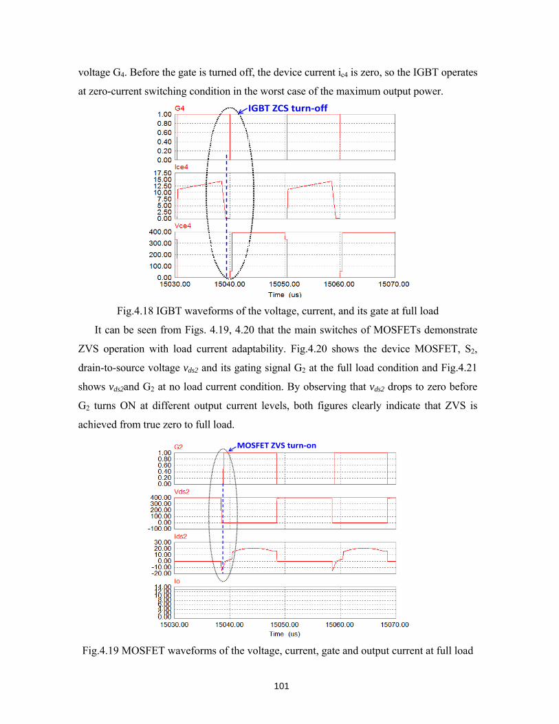
101
voltage G4. Before the gate is turned off, the device current ic4 is zero, so the IGBT operates
at zero-current switching condition in the worst case of the maximum output power.
Fig.4.18 IGBT waveforms of the voltage, current, and its gate at full load
It can be seen from Figs. 4.19, 4.20 that the main switches of MOSFETs demonstrate
ZVS operation with load current adaptability. Fig.4.20 shows the device MOSFET, S2,
drain-to-source voltage vds2 and its gating signal G2 at the full load condition and Fig.4.21
shows vds2and G2 at no load current condition. By observing that vds2 drops to zero before
G2 turns ON at different output current levels, both figures clearly indicate that ZVS is
achieved from true zero to full load.
Fig.4.19 MOSFET waveforms of the voltage, current, gate and output current at full load
IGBT ZCS turn‐off
MOSFET ZVS turn‐on
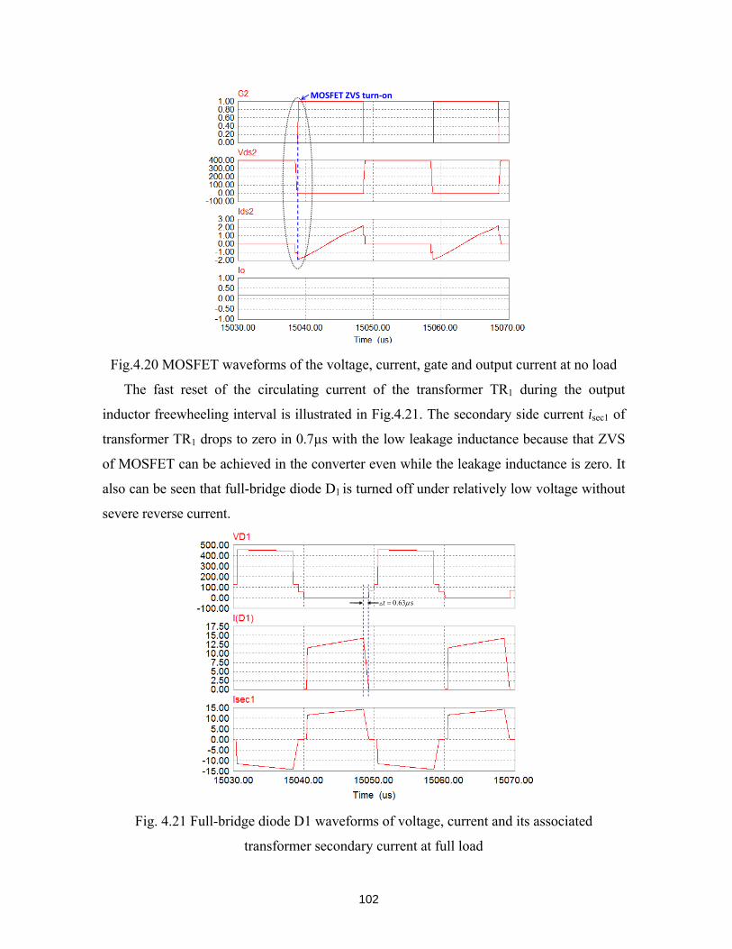
102
Fig.4.20 MOSFET waveforms of the voltage, current, gate and output current at no load
The fast reset of the circulating current of the transformer TR1 during the output
inductor freewheeling interval is illustrated in Fig.4.21. The secondary side current isec1 of
transformer TR1 drops to zero in 0.7µs with the low leakage inductance because that ZVS
of MOSFET can be achieved in the converter even while the leakage inductance is zero. It
also can be seen that full-bridge diode D1 is turned off under relatively low voltage without
severe reverse current.
Fig. 4.21 Full-bridge diode D1 waveforms of voltage, current and its associated
transformer secondary current at full load
MOSFET ZVS turn‐on
0.63t sμ=

103
Fig. 4.22 Half-bridge diode D5 waveforms of voltage and its associated transformer
secondary current at full load
Fig. 4.22 shows the waveforms of the half-bridge diode ZCS turn-on and turn-off in the
worst case of full load condition. The well-clamped voltage stress and ZCS operation of the
half-bridge diode imply that the diode voltage stress is low and the low-voltage drop diode
can be utilized to further improve the efficiency.
4.4 Comparisons between the Proposed and Improved Converters
These two converters have many similarities, which are also their advantages, as follows.
1) With the parallel LLC resonant half-bridge configuration, zero-voltage switching of
MOSFETs in the leading-leg can be ensured from true zero to full load, and thus, the
super-junction MOSFET with slow reverse recovery body diode can be reliably used.
2) IGBTs in the lagging-leg work at zero-current switching with minimum circulating
conduction loss because the parallel secondary-side DC voltage source effectively reset
the circulating current, therefore, the turn-off loss and the conduction loss of the IGBTs
are significantly reduced.
ZCS turn‐onZVS turn‐off

104
3) Duty cycle loss is negligible since the leakage inductance of the main transformer can be
minimized without losing ZVS operation, thus, the current stresses through the primary-
side semiconductors are minimized by the optimized turns ratio of the main transformer.
4) The topologies are suitable for wide-range output voltage or current source applications
because of the buck-type configuration with the simple phase-shift pulse width
modulation, and thus, they are a good candidate for the electrical vehicle battery charger.
And this improved converter demonstrates better performances than the previous
proposed one does.
a) Energy Transfer Method
These two converter topologies are repeated here in Fig.4.23 (a),(b).
(a)The converter proposed in CH3 (b) The improved converter in CH4
Fig. 4.23 Circuit configurations of the two converters
Fig.4.23 (a) shows that the output of LLC half bridge converter and the output of the
phase shifted full bridge are in parallel to get the energy transferred. When it operates at
( )0 / 2eff st D T< < , the phase shifted full bridge converter is in charge to transfer the
energy to the load and no energy stored in C2 or C1 get transferred while the LLC converter
charges the capacitors C1 or C2. Only when it operates at ( )/ 2 1eff sD T t≤ < , the energy
stored in C2 or C1 gets transferred to the load by the LLC converter. Thus when the
effective duty cycle effD approaches one, the energy stored in C2 or C1 has no chance to be
transferred to the load.
1prii 2prii
rectv oV−
+
−
+
1S
2S
3S
4S
1D
2D4D
3D 5D
6D
7D
3C
1C
2C
oL
oRoC
m2Llk1L lk2L
inV1TR
2TR
1SC
2SC
2Lmi1dsv−+
TR1
TR2
1S
2S
3S
4S
1D
2D
5D
6D
3C
4D
3D
1C
2C
oL
oRoC
inV
rectv
−
+
−
+
1prii2priim2Llk1Llk2L
1SC
2SC
1dsv−
+
oV
2Lmi

105
Fig.23 (b) shows that the LLC half bridge converter and the the phase shifted full
bridge are in series to get the energy transferred. When it operates at ( )0 / 2eff st D T< < ,
the phase shifted full bridge converter transfers the energy to the load and also energy
stored in C2 or C1 get transferred to the load while the LLC converter charges the capacitors
C1 or C2. When it operates at ( )/ 2 1eff sD T t≤ < , the energy stored in C2 or C1 gets
transferred to the load by the LLC converter. Thus whatever the effective duty cycle effD
is, the energy stored in C2 or C1 is always transferred to the load.
b) Transformer Size
The secondary rectifier voltage waveforms for these two converters are repeated here
in Fig.4.24.
(a) The converter proposed in CH3 (b) The improved converter in CH4
Fig.4.24 The secondary rectifier voltage waveform
From Fig.4.24, it can be seen that the ratio of the main transformer in the improved
converter can be 0.5n2 smaller than that in the converter proposed in Chapter3 under the
same specifications due to the energy stored in C2 or C1transferred to the load during the
interval ( )0 / 2eff st D T< < .
c) Output Inductor Size
Fig. 4.25 Normalized peak-to-peak output inductor current vs. normalized output voltage
1 inn V
2 inn VoV
rectV
0 t
1 20.5in inn V n V+
2 inn VoV
rectV
0 t(a) (b)
0
0.2
0.4
0.6
0.8
1
0.5 0.6 0.7 0.8 0.9 1
Conventional
Proposed
Improved
Normalized output voltage
Nor
mal
ized
curr
ent r
ippl
e

106
Suppose n1 is the same in the conventional full bridge, the proposed one in Chapter3
and the improved one in this chapter, it can be seen from Fig.4.25 that the output inductor
current ripple in the proposed converter can be reduced by n2/n1 compared to the
conventional full bridge, which means the inductance can be reduced by n2/n1 compared to
the conventional full bridge under the same current ripple condition, and the output
inductor current ripple in the improved converter can be reduced by n2/(2n1-n2)compared to
the conventional full bridge, which means the inductance can be reduced by n2/(2n1-
n2)compared to the conventional full bridge under the same current ripple condition. Thus
the inductance can be reduced by 2 1 2
1 1 2
( )(2 )
n n nn n n
−−
compared to the proposed converter. Since
n2<n1, it can be seen that the improved converter has smallest current ripple.
4.5 Summary
To solve the problem at the certain case in the previous proposed novel hybrid resonant
and PWM converter in chapter 3, an improved hybrid resonant and PWM converter has
been proposed. Its basic operation has been analyzed and verified by simulations. Table 4.2
summarizes the performances of these four converters.
Table 4.2: Phase-shifted full bridge, LLC, Previous Proposed and Improved Converters
Control
method
ZVS
range
Circulating
current
Constant Current
and Voltage
Output diode
voltage stress
PS FB Fixed
frequency
Limited
range High Yes High
LLC Variable
frequency
Full
range Low No Low
Proposed
converter
Fixed
frequency
Full
range Low Yes Low
Improved
converter
Fixed
frequency
Full
range Low Yes Low
From Table 4.2 it can be seen that the improved hybrid converter can keep all the
advantages of the previous proposed converter in chapter 3 repeated as follows:

107
1) With the parallel LLC resonant half-bridge configuration, zero-voltage switching of
MOSFETs in the leading-leg can be ensured from true zero to full load, and thus, the
super-junction MOSFET with slow reverse recovery body diode can be reliably used.
2) IGBTs in the lagging-leg work at zero-current switching with minimum circulating
conduction loss because the parallel secondary-side DC voltage source effectively reset
the circulating current, therefore, the turn-off loss and the conduction loss of the IGBTs
are significantly reduced.
3) Duty cycle loss is negligible since the leakage inductance of the main transformer can
be minimized without losing ZVS operation, thus, the current stresses through the
primary-side semiconductors are minimized by the optimized turns ratio of the main
transformer.
4) The topology is suitable for wide-range output voltage or current source applications
because of the buck-type configuration with the simple phase-shift pulse width
modulation, and thus, it is a good candidate for the electrical vehicle battery charger.
And theoretically the improved converter demonstrates better performances than the
previous proposed one does.
1) The auxiliary transformer is utilized fully since the LLC half bridge converter and the
phase shifted full bridge are in series to get the energy transferred. When it operates at
( )0 / 2eff st D T< < , the phase shifted full bridge converter transfers the energy to the
load and also energy stored in C2 or C1 get transferred to the load while the LLC
converter charges the capacitors C1 or C2. When it operates at ( )/ 2 1eff sD T t≤ < , the
energy stored in C2 or C1 gets transferred to the load by the LLC converter. Thus
whatever the effective duty cycle effD is, the energy stored in C2 or C1 is always
transferred to the load.
2) The main transformer can be smaller. It is 0.5n2 smaller than that in the converter
proposed in Chapter3 under the same specifications due to the energy stored in C2 or
C1transferred to the load during the interval ( )0 / 2eff st D T< < .
3) The output inductor can be smaller than that in the proposed converter in chapter 3.

108
Conclusion
In this thesis, key features of different isolated DC-DC converters are discussed, and
two new hybrid isolated converters are proposed for the EV battery charger application.
The conventional isolated DC-DC converters suitable for high power applications are
phase-shifted full-bridge and LLC converter. Although they are suitable for high efficiency,
high power density and high reliability, they are also limited in some operating ranges. To
make full use of their advantages and to avoid their drawbacks of losing zero-voltage
switching and output regulation, a novel hybrid resonant and PWM converter combining
resonant LLC half-bridge and phase shifted full-bridge topology is proposed for high
efficiency and true full soft-switching range, which is very critical for the battery charger
application because the battery requires a constant current charging with variable voltage
and a constant voltage charging with variable current. A 3.4-kW hardware prototype has
been designed, implemented and tested to verify that the proposed hybrid converter truly
avoids the conventional converters while maintaining their advantages. In this proposed
hybrid converter, the utilization efficiency of the auxiliary transformer is not that ideal.
When the duty cycle is large, LLC converter charges one of the capacitors but the energy
stored in the capacitor has no chance to be transferred to the output, resulting in the low
utilization efficiency of the auxiliary transformer. To utilize the auxiliary transformer fully
while keeping all the prominent features of the previous hybrid converter, an improved
hybrid resonant and PWM converter is proposed, and its basic operation is analyzed and
simulated to verify the validity.
These two proposed converters show some common advantages as described below.
1) With the parallel LLC resonant half-bridge configuration, zero-voltage switching of
MOSFETs in the leading-leg can be ensured from true zero to full load, and thus, the
super-junction MOSFET with slow reverse recovery body diode can be reliably used.
2) IGBTs in the lagging-leg work at zero-current switching with minimum circulating
conduction loss because the parallel secondary-side DC voltage source effectively reset
the circulating current, therefore, the turn-off loss and the conduction loss of the IGBTs
are significantly reduced.

109
3) Duty cycle loss is negligible since the leakage inductance of the main transformer can be
minimized without losing ZVS operation, thus, the current stresses through the primary-
side semiconductors are minimized by the optimized turns ratio of the main transformer.
4) The topologies are suitable for wide-range output voltage or current source applications
because of the buck-type configuration with the simple phase-shift pulse width
modulation, and thus, they are a good candidate for the electrical vehicle battery charger.
The improved hybrid converter demonstrates some additional advantages:
1) The auxiliary transformer is utilized fully since the output of the LLC resonant converter
is in series with the output load, thus the energy stored in the capacitor can be transferred
to the output.
2) The main transformer can be smaller because the energy stored in the capacitor, which
was charged by the LLC converter in the last effective duty cycle, can be transferred to
the output during the effective duty cycle.
3) The output inductor of the improved hybrid converter can be smaller than that of the
first proposed hybrid converter.

110
References [1] Texas Instruments, “Hybrid and Electric Vehicle Solutions Guide”,
http://www.ti.com/lit/ml/szza058a/szza058a.pdf
[2] K. T. Chau and Y. S. Wong, “Overview of power management in hybrid electric
vehicles”, Energy Conversion and Management, vol. 43, Issue 15, pp. 1953-1968,
2002.
[3] Pesaran, “Battery Requirements for Plug-In Hybrid Electric Vehicles – Analysis and
Rational”, presented in Sustainability: The Future of Transportation, EVS, Dec. 2007.
[4] L. Siguang, Z. Chengning, and X. Shaobo, “Research on Fast Charge Method for
Lead-acid Electric Vehicle Batteries”, in Proc. IEEE ISA’09, May 2009, pp. 1-5.
[5] Richard Redl, “Batteries for Beginners” in Proc. APEC, Feb.5-9, 2012, pp.
[6] M.C. Kisacikoglu, B. Ozpineci, L.M. Tolbert, “Reactive power operation analysis of
a single-phase EV/PHEV bidirectional battery charger,” Power Electronics and
ECCE Asia (ICPE & ECCE), 2011 IEEE 8th International Conference on , vol., no.,
pp.585-592, May 30 2011-June 3 2011
[7] G. Glanzer, T. Sivaraman, J.I. Buffalo, M. Kohl, H. Berger, "Cost-efficient
integration of electric vehicles with the power grid by means of smart charging
strategies and integrated on-board chargers," Environment and Electrical
Engineering (EEEIC), 2011 10th International Conference on , vol., no., pp.1-4, 8-
11 May 2011
[8] C.B. Toepfer, “Charge! EVs power up for the long haul,” Spectrum, IEEE , vol.35,
no.11, pp.41-47, Nov 1998
[9] Erb, D.C.; Onar, O.C.; Khaligh, A.; , "Bi-directional charging topologies for plug-in
hybrid electric vehicles," Applied Power Electronics Conference and Exposition
(APEC), 2010 Twenty-Fifth Annual IEEE , vol., no., pp.2066-2072, 21-25 Feb. 2010
[10] Jim Francfort, Electric Vehicle Charging Levels and Requirements Overview” ,
Clean Cities December 2010 Webinar, http://www1.eere.energy.gov
[11] Ingram, “Charging your electric car at home: What you need to know”, Venture Beat,
August 13, 2010.

111
[12] Nissan; “Charging FAQ”, [online]. Available: http://www.nissanusa.com/leaf-
electriccar/faq/list/charging#/leaf-electric-car/faq/list/charging
[13] NEC Corporation of America, “Portland General Electric Opens North America’s
First Public-Use Quick-Charge Station,” Portland, OR, August 5, 2010.
[14] SAE International, “Ground Vehicle Standards Newsletter”,vol. 1, issue 3, October
2010.
[15] X. Navarro, “The European standard charging plug for cars is selected after
Mennekes design” Autoblog, May 20, 2009.
[16] CHAdeMO, “What is CHAdeMO?” [Online]. Available:
http://chademo.com/01_What_is_CHAdeMO.html
[17] R.Surada, and A. Khaligh, "A novel approach towards integration of propulsion
machine inverter with energy storage charger in plug-in hybrid electric vehicles," in
Proc.IECON’10, Nov. 7-10, 2010, pp. 2493-2498.
[18] Chan, C.C. and Chau, K.T., "An overview of power electronics in electric vehicles,"
IEEE Trans. on Industrial Electronics, Volume 44, Issue 1, February 1997, Page(s):
3 – 13.
[19] J. G. Hayes, "Battery Charging Systems for Electric Vehicles," Electric Vehicles - A
Technology Roadmap for the Future," Digest No. 1998/262, IEE Colloquium on
page(s): 4/1-4/8, May 1998.
[20] I.A. Khan, "Battery chargers for electric and hybrid vehicles," Power Electronics in
Transportation, Proceedings, 20-21 Oct. 1994, Page(s): 103-112.
[21] K. Jin, X. Ruan, M. Yang, and M. Xu, “A Hybrid Fuel Cell Power System”, IEEE
Trans Ind. Electron., vol. 56, no. 4, pp. 1212-1222, 2009.
[22] J. Zhang, C.Y. Lin, X. Zhuang, K. Rinne, D. Sable, G. Hua and F.C. Lee, “Design of
A 4kw On-Board Battery Charger for Electric Vehicle,” Annual VPEC Seminar,
September 1995.
[23] W. Andreycak, “Active Clamp and Reset Technique Enhances Forward Converter
Performance,” in Unitrode Power Supply Design Seminar, 1994.
[24] T. Ninomiya, N. Matsumoto, M. Nakahara, and K. Harada, “Static And Dynamic
analysis of Zero-Voltage-Switched Half-Bridge Converter with PWM Control,”
IEEE PESC, 1991.

112
[25] Y.-C. Chuang and Y.-L. Ke, “A novel high-efficiency battery charger with a buck
zero-voltage-switching resonant converter,” IEEE Trans. Energy Convers., vol. 22,
no. 4, pp. 848–854, Dec. 2007.
[26] Y.-C. Chuang and Y.-L. Ke, “High-efficiency and low-stress ZVT-PWM DC-to-DC
converter for battery charger,” IEEE Trans. Ind. Electron., vol. 55, no. 8, pp. 3030–
3037, Aug. 2008.
[27] Y.-C. Chuang, Y.-L. Ke, and S.-Y. Chang, “Highly-efficient battery chargers with
parallel-loaded resonant converters,” in Conf. Rec. IEEE IAS Annu. Meeting, Oct.
4–8, 2009, pp. 1–10.
[28] O. D. Patterson and D. M. Divan, “Pseudo-resonant full bridge DC/DC converter,”
IEEE Trans. Power Electron., vol. 6, no. 4, pp. 671–678, Oct. 1991.
[29] M. Nakaoka, S. Nagai, Y. J. Kim, Y. Ogino, and Y. Murakami, “The state-of-the-art
phase-shifted ZVS-PWM series and parallel resonant DC–DC power converters
using internal parasitic circuit components and new digital control,” in Conf. Rec.
IEEE 23rd Annu. PESC, Jun. 29–Jul. 3, 1992, vol. 1, pp. 62–70.
[30] P. K. Jain, W. Kang, H. Soin, and Y. Xi, “Analysis and design considerations of a
load and line independent zero voltage switching full bridge DC/DC converter
topology,” IEEE Trans. Power Electron., vol. 17, no. 5, pp. 649–657, Sep. 2002.
[31] M. Pahlevaninezhad, J. Drobnik, P.K. Jain, A. Bakhshai, “A Load Adaptive Control
Approach for a Zero-Voltage-Switching DC/DC Converter Used for Electric
Vehicles,” Industrial Electronics, IEEE Transactions on , vol.59, no.2, pp.920-933,
Feb. 2012
[32] Loveday.H,Weene; chris A. Wright; “A 1 kW, 500 kHr front-end convener for a
distributed power supply system” APEC’ 89 1989. pp.423-432
[33] J.A. sabate; V.Vlatkovic; R.B, Redley; F.C,Lee; “Design considerations for high-
voltage high-power full-bridge zero-voltage-switched PWM converter” 1990.
APEC‘90.pp.275-284
[34] R. Steigerwald, “A Comparison of Half-Bridge Resonant Converter Topologies,” in
IEEE Trans. on Power Electronics, Vol. 3, No. 2, pp. 174-182, April 1988.
[35] Texas Instrument, “Power supply topologies”, [Online], available:
http://www.ti.com/lit/sg/sluw001d/sluw001d.pdf

113
[36] R. Severns, “Topologies for Three Elements Resonant Converters,” in IEEE APEC
Rec., 1990, pp. 712-722.
[37] R. Oruganti and F.C. Lee, “Resonant Power Processors, Part 2: Methods of Control,”
IEEE Trans. on Industrial Application, 1985.
[38] R. Severns, “Topologies For Three Element Resonant Converters,” Proc. IEEE
APEC ’90, 1990, pp. 712-722.
[39] VatcheVorperian, Analysis Of Resonant Converters, Dissertation, California
Institute of Technology, 1984.
[40] R. Farrington, M.M. Jovanovic, and F.C. Lee, “Analysis of Reactive Power in
Resonant Converters,” Proc. IEEE PESC ’92, 1992.
[41] P. Calderira, R. Liu, D. Dalal, W.J. Gu, “Comparison of EMI Performance of PWM
and Resonant Power Converters,” Proc. IEEE PESC ’93, 1993, pp. 134-140.
[42] T. Higashi, H. Tsuruta, M. Nakahara, “Comparison of Noise Characteristics for
Resonant and PWM Flyback Converters,” Proc. IEEE PESC ’98, 1998, pp. 689-695.
[43] K.H. Liu, “Resonant Switches Topologies and Characteristics,” Proc. IEEE
PESC’85, 1985, pp. 106-116.
[44] Gyu-YeongChoe; Jong-Soo Kim; Byoung-Kuk Lee; Chung-Yuen Won; Tea-Won
Lee; , "A Bi-directional battery charger for electric vehicles using photovoltaic PCS
systems," Vehicle Power and Propulsion Conference (VPPC), 2010 IEEE , vol., no.,
pp.1-6, 1-3 Sept. 2010
[45] J. O. Groves and F. C. Lee, “Small Signal Analysis of Systems with Periodic
Operating Trajectories,” Proc. VPEC Annual Seminar, 1988, pp. 224-235.
[46] J. O. Groves, “Small-Signal Analysis Using Harmonic Balance Methods,” Proc.
IEEE PESC, 1991, pp. 74–79.
[47] E. X. Yang, “Extended Describing Function Method for Small-Signal Modeling of
Switching Power Circuit,” Proc. VPEC Annual Seminar, 1994, pp.87-96.
[48] E. X. Yang, F. C. Lee and M. Jovanovic, “Small-Signal Modeling of Series and
Parallel Resonant Converters,” Proc. IEEE APEC, 1992, pp. 785-792.
[49] Eric X. Yang,Extended Describing Function Method for Small-Signal Modeling of
Resonant and Multi-Resonant Converters, Dissertation, Virginia Tech, Blacksburg,
VA, February 1994.

114
[50] R.C. Wong and J. O. Groves, “An Automated Small-Signal Frequency- Domain
Analyzer for General Periodic-Operating Systems as Obtained via Time-Domain
Simulation,” Proc. IEEE PESC, 1995, pp. 801-808.
[51] R. Oruganti, J. Yang, and F.C. Lee, “State Plane Analysis of Parallel Resonant
Converters,” Proc. IEEE PESC ’85, 1985.
[52] R. Liu, I. Batarseh, C.Q. Lee, “Comparison of Capacitively and Inductively Coupled
Parallel Resonant Converters,” IEEE Trans. on Power Electronics, 1993, pp. 445-
454, vol.8, issue 4.
[53] M. Emsermann, “An Approximate Steady State and Small Signal Analysis of the
Parallel Resonant Converter Running Above Resonance,” Proc. Power Electronics
and Variable Speed Drives ’91, 1991, pp. 9-14.
[54] Y.G. Kang, A.K. Upadhyay, D. Stephens, “Analysis and Design of a Half Bridge
Parallel Resonant Converter Operating Above Resonance,” Proc. IEEE IAS ’98,
1998, pp. 827-836.
[55] Robert L. Steigerwald, “A Comparison of Half Bridge Resonant Converter
Topologies,” IEEE Trans. on Power Electronics, 1988, pp. 174-182.
[56] M. Zaki, A. Bonsall, I. Batarseh, “Performance Characteristics for the Series Parallel
Resonant Converter,” Proc. Southcon ’94, 1994, pp.573-577.
[57] A.K.S. Bhat, “Analysis, Optimization and Design of a Series Parallel Resonant
Converter,” Proc. IEEE APEC ’90, 1990, pp. 155-164.
[58] Fairchild Semiconductor Corporation, “Application Note AN-4151: Half Bridge
LLC Resonant Converter Design Using FSFR-series Fairchild Power Switch”
Rev1.0.0, 10/09/2007
[59] STMicroelectronics, “Application Note AN-2450: LLC resonant half-bridge
converter design guideline”, Rev5, 10/2007
[60] Microchip Technology Inc. “AN1336: DC/DC LLC Reference Design Using the
dsPIC® DSC” , 2010
[61] R. Ayyanar and N. Mohan, “Novel soft-switching DC–DC converter with full ZVS-
range and reduced filter requirement. I. Regulated-output applications,” IEEE Trans.
Power Electron., vol. 16, no. 2, pp. 184–192, Mar. 2001.

115
[62] G. Hua, F. C. Lee, and M. M. Jovanovic, “An improved zero-voltage switched PWM
converter using a saturable inductor,” in Conf. Rec. IEEE 22nd Annu. PESC, Jun.
24–27, 1991, pp. 189–194.
[63] Z. Amjadi and S. S. Williamson, “Power-electronics-based solutions for plug-in
hybrid electric vehicle energy storage and management systems,” IEEE Trans. Ind.
Electron., vol. 57, no. 2, pp. 608–616, Feb. 2010.
[64] M. Van Wieringen and R. Pop-Iliev, “Development of a dual-fuel power generation
system for an extended range plug-in hybrid electric vehicle,” IEEE Trans. Ind.
Electron., vol. 57, no. 2, pp. 641–648, Feb. 2010.
[65] F. L. Mapelli, D. Tarsitano, andM.Mauri, “Plug-in hybrid electric vehicle: Modeling,
prototype realization, and inverter losses reduction analysis,” IEEE Trans. Ind.
Electron., vol. 57, no. 2, pp. 598–607, Feb. 2010.
[66] Bo Yang, “Topology Investigation for Front End DC/DC Power Conversion for
Distributed Power System”, Ph.D Dissertation 2003, Virginia Polytechnic Institute
and State University.
[67] Hidekazu Miwa, “High-Efficiency Low-Voltage High-Current Power Stage Design
Considerations for Fuel Cell Power Conditioning Systems”, M.S Thesis 2009,
Virginia Polytechnic Institute and State University.
[68] Infineon, “Application Note: MOSFET Power Losses Calculation Using the Data-
Sheet Parameters”, Rev1.1, July, 2006.
[69] Infineon, “Application Note: IGBT Power Losses Calculation Using the Data-
Sheet Parameters”, Rev1.1, January, 2009.