Embed Size (px)
Citation preview

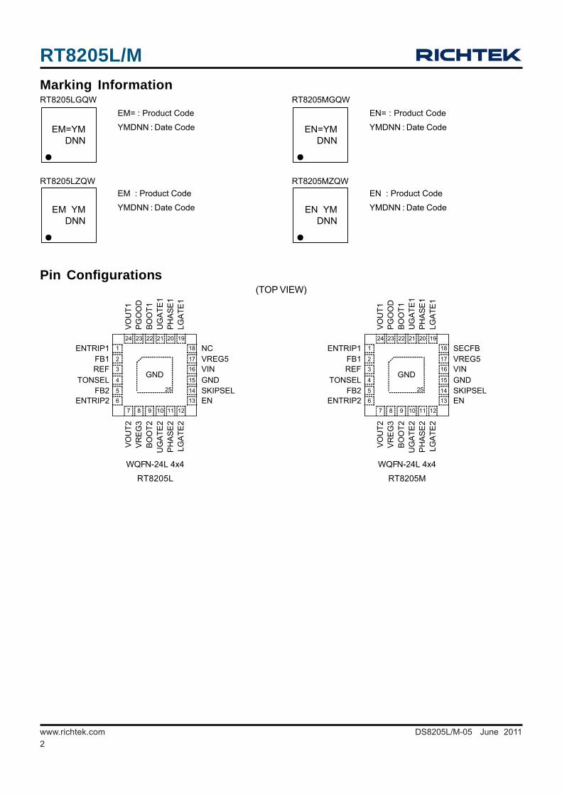
RT8205L/M
1DS8205L/M-05 June 2011 www.richtek.com
ApplicationsNotebook and Sub-Notebook Computers3-Cell and 4-Cell Li+ Battery-Powered Devices
High Efficiency, Main Power Supply Controllerfor Notebook ComputerGeneral DescriptionThe RT8205L/M is a dual step-down, switch mode powersupply controller generating logic-supply voltages inbattery powered systems. It includes two Pulse-WidthModulation (PWM) controllers adjustable from 2V to 5.5V,and also features fixed 5V/3.3V linear regulators. Eachlinear regulator provides up to 100mA output current withautomatic linear regulator bootstrapping to the PWMoutputs. An optional external charge pump can bemonitored through SECFB (RT8205M). The RT8205L/Mincludes on-board power up sequencing, a power goodoutput, internal soft-start, and internal soft-dischargeoutput that prevents negative voltage during shutdown.
The constant on-time PWM control scheme operateswithout sense resistors and provides 100ns response toload transient response while maintaining nearly constantswitching frequency. To eliminate noise in audioapplications, an ultrasonic mode is included, whichmaintains the switching frequency above 25kHz. Moreover,the diode-emulation mode maximizes efficiency for lightload applications. The RT8205L/M is available in aWQFN-24L 4x4 package.
FeaturesConstant On-time Control with 100ns Load StepResponseWide Input Voltage Range : 6V to 25VDual Adjustable Outputs from 2V to 5.5VSecondary Feedback Input Maintains Charge PumpVoltage (RT8205M)Fixed 3.3V and 5V LDO Output : 100mA2V Reference VoltageFrequency Selectable via TONSEL Setting4700ppm/°°°°°C RDS(ON) Current SensingProgrammable Current Limit Combined withEnable ControlSelectable PWM, DEM, or Ultrasonic ModeInternal Soft-Start and Soft-DischargeHigh Efficiency up to 97%5mW Quiescent Power DissipationThermal ShutdownRoHS Compliant and Halogen Free
Ordering Information
Note :
Richtek products are :
RoHS compliant and compatible with the current require-
ments of IPC/JEDEC J-STD-020.
Suitable for use in SnPb or Pb-free soldering processes.
Package TypeQW : WQFN-24L 4x4 (W-Type)
Lead Plating SystemG : Green (Halogen Free and Pb Free)Z : ECO (Ecological Element with Halogen Free and Pb free)
RT8205
Pin FunctionL : DefaultM : With SECFB
RT8205L/M
2DS8205L/M-05 June 2011www.richtek.com
Pin Configurations(TOP VIEW)
WQFN-24L 4x4
RT8205M
WQFN-24L 4x4
RT8205L
ENTRIP1FB1REF
TONSELFB2
ENTRIP2
LGAT
E2
VOU
T2V
RE
G3
BO
OT2
PH
AS
E2
UG
ATE
2
NCVREG5
GNDSKIPSELEN
VIN
UG
ATE
1
LGA
TE1
VOU
T1PG
OO
DBO
OT1
PHA
SE1
GND
1
2
3
4
5
6
7 8 9 10 1211
18
17
16
15
14
13
21 20 1924 2223
25
ENTRIP1FB1REF
TONSELFB2
ENTRIP2
LGAT
E2
VOU
T2V
RE
G3
BO
OT2
PH
AS
E2
UG
ATE
2
SECFBVREG5
GNDSKIPSELEN
VIN
UG
ATE
1
LGA
TE1
VOU
T1PG
OO
DBO
OT1
PHA
SE1
GND
1
2
3
4
5
6
7 8 9 10 1211
18
17
16
15
14
13
21 20 1924 2223
25
EM=YMDNN
EN=YMDNN
Marking Information
EM= : Product Code
YMDNN : Date Code
EN= : Product Code
YMDNN : Date Code
RT8205MGQWRT8205LGQW
EM : Product Code
YMDNN : Date Code
EN : Product Code
YMDNN : Date Code
RT8205MZQWRT8205LZQW
EM YMDNN
EN YMDNN
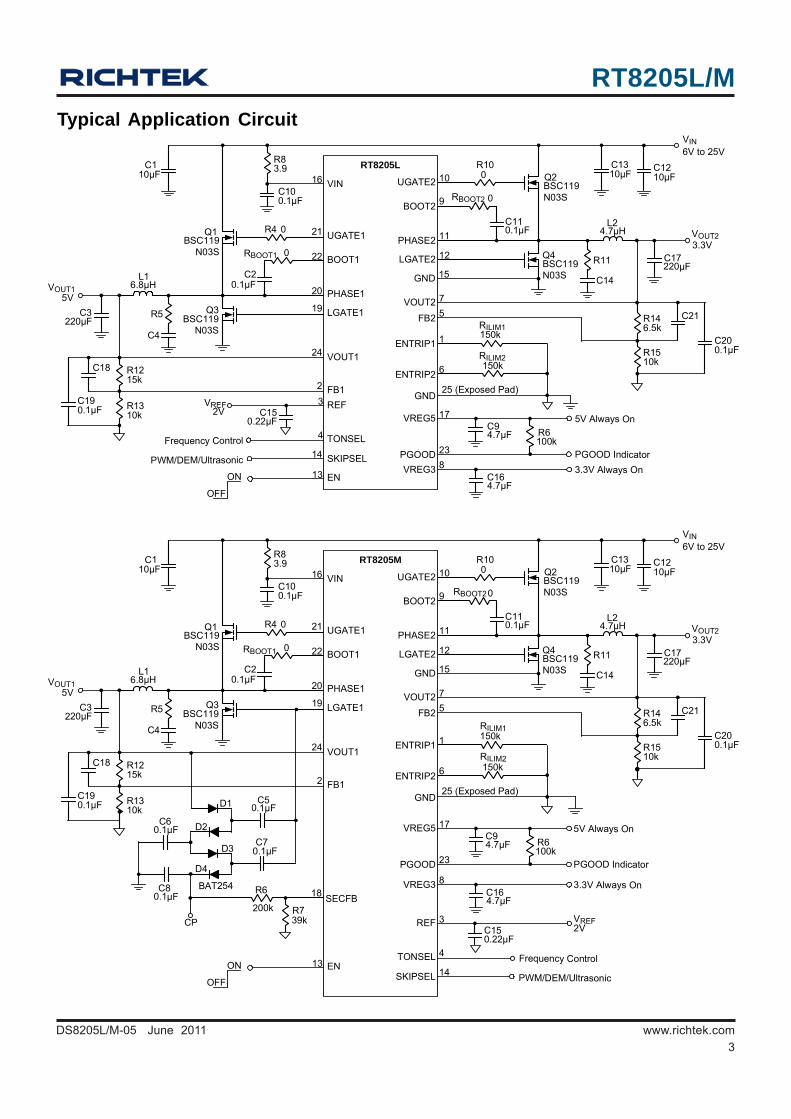
RT8205L/M
3DS8205L/M-05 June 2011 www.richtek.com
Typical Application Circuit
RT8205L
PHASE1
LGATE1
BOOT1
UGATE1
VOUT1
VOUT15V
VIN
VREG5
VREG3PGOOD
GND
16
25 (Exposed Pad)
19
22
20
21
24
23
17
8
PHASE2
LGATE2
BOOT2
UGATE2
VOUT2
VOUT2
Q2
L2C11
C173.3V
R10 C12
VIN
10µF 10µF
0.1µF
R11
C14
10
11
9
12
7
BSC119N03S
Q4BSC119N03S
0
RBOOT2 0
C13
4.7µH
220µF
Q1
L1 C2
C3
R4
10µF
0.1µF
R5
C4
BSC119N03S
Q3BSC119
N03S
0
RBOOT1 0
C1
6.8µH
220µF
R83.9
C100.1µF
5V Always On
3.3V Always On
ENTRIP1
ENTRIP2
1
6
FB2
FB12
5RILIM1150k
150k
C94.7µF R6
100kPGOOD Indicator
C164.7µF
REF3C15
0.22µF
TONSEL
SKIPSEL
4
14Frequency Control
PWM/DEM/Ultrasonic
ENON
OFF
13
R146.5k
R1510k
C21
C200.1µF
R1215k
R1310k
C18
C190.1µF
GND 15
6V to 25V
VREF2V
RILIM2
RT8205M
PHASE1
LGATE1
BOOT1
UGATE1
VOUT1
VOUT15V
VIN
VREG5
VREG3
PGOOD
GND
16
25 (Exposed Pad)
19
22
20
21
24
23
17
8
PHASE2
LGATE2
BOOT2
UGATE2
VOUT2
VOUT2
Q2
L2C11
C173.3V
R10 C12
VIN
10µF 10µF
0.1µF
R11
C14
10
11
9
12
7
BSC119N03S
Q4BSC119N03S
0
0
C13
4.7µH
220µF
Q1
L1 C2
C3
R4
10µF
0.1µF
R5
C4
BSC119N03S
Q3BSC119
N03S
0
0
C1
6.8µH
220µF
R83.9
C100.1µF
5V Always On
3.3V Always On
ENTRIP1
ENTRIP2
1
6
FB2
FB12
5
150k
150k
C94.7µF R6
100kPGOOD Indicator
C164.7µF
ENON
OFF
13
R146.5k
R1510k
C21
C200.1µF
R1215k
R1310k
C18
C190.1µF
GND 15
6V to 25V
C50.1µF
C70.1µF
SECFB18R6
R739kCP
D1
D2
D3
D4
C60.1µF
C80.1µF
BAT254
200kREF 3
C150.22µF
TONSEL
SKIPSEL
4
14Frequency Control
PWM/DEM/Ultrasonic
VREF2V
RBOOT1
RBOOT2
RILIM1
RILIM2
RT8205L/M
4DS8205L/M-05 June 2011www.richtek.com
Functional Pin DescriptionPin No. Pin Name Pin Function
1 ENTRIP1
Channel 1 Enable and Current Limit Setting Input. Connect a resistor to GND to set the threshold for channel 1 synchronous RDS(ON) sense. The GND − PHASE1 current limit threshold is 1/10th the voltage seen at ENTRIP1 over a 0.515V to 3V range. There is an internal 10μA current source from VREG5 to ENTRIP1. Leave ENTRIP1 floating or drive it above 4.5V to shutdown channel 1.
2 FB1 SMPS1 Feedback Input. Connect FB1 to a resistive voltage divider from VOUT1 to GND to adjust output from 2V to 5.5V.
3 REF 2V Reference Output. Bypass to GND with a minimum 0.22μF capacitor. REF can source up to 100μA for external loads. Loading REF degrades FBx and output accuracy according to the REF load regulation error.
4 TONSEL
Frequency Selectable Input for VOUT1/VOUT2 respectively. 400kHz/500kHz : Connect to VREG5 or VREG3 300kHz/375kHz : Connect to REF 200kHz/250kHz : Connect to GND
5 FB2 SMPS2 Feedback Input. Connect FB2 to a resistive voltage divider from VOUT2 to GND to adjust output from 2V to 5.5V.
6 ENTRIP2
Channel 2 Enable and Current Limit Setting Input. Connect a resistor to GND to set the threshold for channel 2 synchronous RDS(ON) sense. The GND − PHASE2 current limit threshold is 1/10th the voltage seen at ENTRIP2 over a 0.515V to 3V range. There is an internal 10μA current source from VREG5 to ENTRIP2. Leave ENTRIP2 floating or drive it above 4.5V to shutdown channel 1.
7 VOUT2 Bypass Pin for SMPS2. Connect to the SMPS2 output to bypass efficient power for VREG3 pin. VOUT2 is also for the SMPS2 output soft-discharge.
8 VREG3 3.3V Linear Regulator Output.
9 BOOT2 Boost Flying Capacitor Connection for SMPS2. Connect to an external capacitor according to the typical application circuits.
10 UGATE2 Upper Gate Driver Output for SMPS2. UGATE2 swings between PHASE2 and BOOT2.
11 PHASE2 Switch Node for SMPS2. PHASE2 is the internal lower supply rail for the UGATE2 high side gate driver. PHASE2 is also the current sense input for the SMPS2.
12 LGATE2 Lower Gate Drive Output for SMPS2. LGATE2 swings between GND and VREG5.
13 EN Master Enable Input. The REF/VREG5/VREG3 are enabled if it is within logic high level and disabled if it is less than the logic low level.
14 SKIPSEL
Operation Mode Selectable Input. Connect to VREG5 or VREG3 : Ultrasonic Mode Connect to REF : DEM Mode Connect to GND : PWM Mode
15, 25 (Exposed Pad) GND Ground for SMPS Controller. The exposed pad must be soldered to a large PCB
and connected to GND for maximum power dissipation. 16 VIN Supply Input for 5V/3.3V LDO and Feed Forward On Time Circuitry.
17 VREG5 5V Linear Regulator Output. VREG5 is also the supply voltage for the lower gate driver and analog supply voltage for the device.
To be continued
RT8205L/M
5DS8205L/M-05 June 2011 www.richtek.com
Pin No. Pin Name Pin Function NC (RT8205L) No Internal Connection.
18 SECFB (RT8205M)
Charge Pump Control Pin. The SECFB is used to monitor the optional external 14V charge pump. Connect a resistive voltage divider from the 14V charge pump output to GND to detect the output. If SECFB drops below the threshold voltage, LGATE1 will provide 33kHz switching frequency for the charge pump. This will refresh the external charge pump driven by LGATE1 without over discharging the output voltage.
19 LGATE1 Lower Gate Drive Output for SMPS1. LGATE1 swings between GND and VREG5.
20 PHASE1 Switch Node for SMPS1. PHASE1 is the internal lower supply rail for the UGATE1 high side gate driver. PHASE1 is also the current sense input for the SMPS1.
21 UGATE1 Upper Gate Driver Output for SMPS1. UGATE1 swings between PHASE1 and BOOT1.
22 BOOT1 Boost Flying Capacitor Connection for SMPS1. Connect to an external capacitor according to the typical application circuits.
23 PGOOD Power Good Output for Channel 1 and Channel 2. (Logical AND)
24 VOUT1 Bypass Pin for SMPS1. Connect to the SMPS1 output to bypass efficient power for VREG5 pin. VOUT1 is also for the SMPS1 output soft-discharge.
Function Block Diagram
SMPS2 PWM Buck Controller
BOOT2
UGATE2
PHASE2
LGATE2
GND
VREG5
VOUT2FB2ENTRIP2
PGOOD
SMPS1 PWM Buck Controller
BOOT1
UGATE1
PHASE1
LGATE1
VREG5
VOUT1
FB1ENTRIP1
VREG5
ThermalShutdown
REF
SW5 Threshold
TONSEL SKIPSEL
VIN
VREG5
Power-OnSequence
Clear Fault Latch
EN
VREG3
SW3 Threshold
REF
VREG3
VREG5VREG5
RT8205L/M
6DS8205L/M-05 June 2011www.richtek.com
Absolute Maximum Ratings (Note 1)
VIN, EN to GND ----------------------------------------------------------------------------------------------- −0.3V to 30VPHASEx to GND
DC ---------------------------------------------------------------------------------------------------------------- −0.3V to 30V < 20ns----------------------------------------------------------------------------------------------------------- −8V to 38V
BOOTx to PHASEx ------------------------------------------------------------------------------------------ −0.3V to 6VENTRIPx, SKIPSEL, TONSEL, PGOOD to GND ------------------------------------------------------ −0.3V to 6VVREG5, VREG3, FBx , VOUTx, SECFB, REF to GND---------------------------------------------- −0.3V to 6VUGATEx to PHASEx
DC ---------------------------------------------------------------------------------------------------------------- −0.3V to (VREG5 + 0.3V) < 20ns----------------------------------------------------------------------------------------------------------- −5V to 7.5V
LGATEx to GND DC ---------------------------------------------------------------------------------------------------------------- −0.3V to (VREG5 + 0.3V) < 20ns----------------------------------------------------------------------------------------------------------- −2.5V to 7.5V
Power Dissipation, PD @ TA = 25°C WQFN-24L-4x4 ------------------------------------------------------------------------------------------------ 1.923W
Package Thermal Resistance (Note 2)WQFN-24L-4x4, θJA ------------------------------------------------------------------------------------------ 52°C/WWQFN-24L-4x4, θJC ------------------------------------------------------------------------------------------ 7°C/WLead Temperature (Soldering, 10 sec.) ------------------------------------------------------------------ 260°CJunction Temperature ---------------------------------------------------------------------------------------- 150°CStorage Temperature Range -------------------------------------------------------------------------------- −65°C to 150°CESD Susceptibility (Note 3)HBM (Human Body Mode) ---------------------------------------------------------------------------------- 2kVMM (Machine Mode) ----------------------------------------------------------------------------------------- 200V
Recommended Operating Conditions (Note 4)
Supply Input Voltage, VIN ----------------------------------------------------------------------------------- 6V to 25VJunction Temperature Range ------------------------------------------------------------------------------- −40°C to 125°CAmbient Temperature Range ------------------------------------------------------------------------------- −40°C to 85°C
RT8205L/M
7DS8205L/M-05 June 2011 www.richtek.com
To be continued
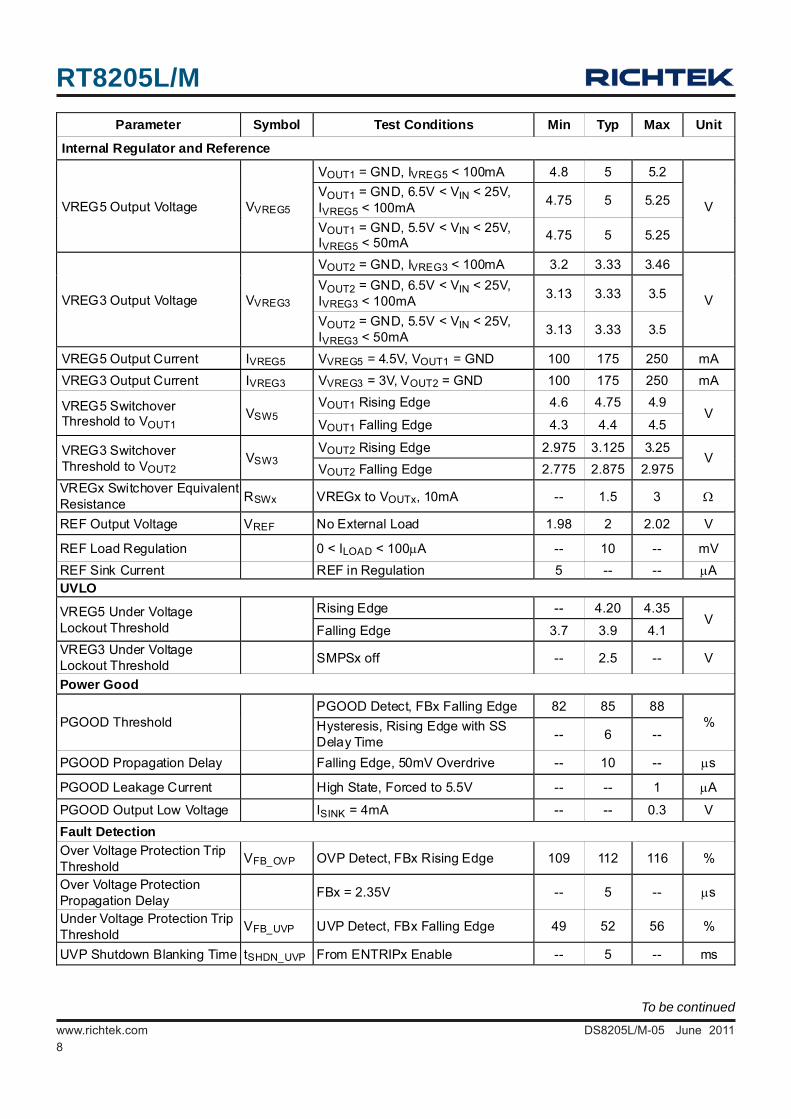
Electrical Characteristics (VIN = 12V, VEN = 5V, VENTRIP1 = VENTRIP2 = 2V, No Load, TA = 25°C, unless otherwise specified)
Parameter Symbol Test Conditions Min Typ Max Unit Input Supply
VIN Standby Current IVIN_SBY VIN = 6V to 25V, ENTRIPx = GND -- 200 -- μA
VIN Shutdown Supply Current IVIN_SHDN VIN = 6V to 25V,
ENTRIPx = EN = GND -- 20 40 μA
Quiescent Power Consumption
PVIN +PPVCC
Both SMPS On, VFBx = 2.1V, SKIPSEL = REF, VOUT1 = 5V, VOUT2 = 3.3V (Note 5)
-- 5 7 mW
SMPS Output and FB Voltage DEM Mode 1.975 2 2.025
PWM Mode (Note 6) -- 2 -- FBx Voltage VFBx
Ultrasonic Mode -- 2.032 --
V
SECFB Voltage VSECFB 1.92 2 2.08 V Output Voltage Adjust Range VOUTx SMPS1, SMPS2 2 -- 5.5 V
VOUTx Discharge Current VOUTx = 0.5V, VENTRIPx = 0V 10 45 -- mA
On-Time VOUT1 = 5.05V (200kHz) 1895 2105 2315
TONSEL = GND VOUT2 = 3.33V (250kHz) 999 1110 1221 VOUT1 = 5.05V (300kHz) 1227 1403 1579
TONSEL = REF VOUT2 = 3.33V (375kHz) 647 740 833 VOUT1 = 5.05V (400kHz) 895 1052 1209
On-Time Pulse Width tON
TONSEL = VREG5 VOUT2 = 3.33V (500kHz) 475 555 635
ns
Minimum Off-Time tOFF FBx = 1.9V 200 300 400 ns Ultrasonic Mode Frequency SKIPSEL = VREG5 or VREG3 22 33 -- kHz
Soft-Start Soft-Start Time tSSx Internal Soft-Start -- 2 -- ms Current Sense ENTRIPx Source Current IENTRIPx VENTRIPx = 0.9V 9.4 10 10.6 μA
ENTRIPx Current Temperature Coefficient
TCIENTRIPx In Comparison with 25°C (Note 6) -- 4700 -- ppm/°C
ENTRIPx Adjustment Range VENTRIPx = IENTRIPx x RENTRIPx 0.515 -- 3 V
Current Limit Threshold GND − PHASEx, VENTRIPx = 2V 180 200 220 mV
Zero-Current Threshold GND − PHASEx in DEM -- 3 -- mV
RT8205L/M
8DS8205L/M-05 June 2011www.richtek.com
To be continued
Parameter Symbol Test Conditions Min Typ Max Unit
Internal Regulator and Reference
VREG5 Output Voltage VVREG5
VOUT1 = GND, IVREG5 < 100mA 4.8 5 5.2
V VOUT1 = GND, 6.5V < VIN < 25V, IVREG5 < 100mA 4.75 5 5.25
VOUT1 = GND, 5.5V < VIN < 25V, IVREG5 < 50mA 4.75 5 5.25
VREG3 Output Voltage VVREG3
VOUT2 = GND, IVREG3 < 100mA 3.2 3.33 3.46
V VOUT2 = GND, 6.5V < VIN < 25V, IVREG3 < 100mA 3.13 3.33 3.5
VOUT2 = GND, 5.5V < VIN < 25V, IVREG3 < 50mA 3.13 3.33 3.5
VREG5 Output Current IVREG5 VVREG5 = 4.5V, VOUT1 = GND 100 175 250 mA VREG3 Output Current IVREG3 VVREG3 = 3V, VOUT2 = GND 100 175 250 mA
VREG5 Switchover Threshold to VOUT1 VSW5
VOUT1 Rising Edge 4.6 4.75 4.9 V
VOUT1 Falling Edge 4.3 4.4 4.5
VREG3 Switchover Threshold to VOUT2 VSW3
VOUT2 Rising Edge 2.975 3.125 3.25 V
VOUT2 Falling Edge 2.775 2.875 2.975 VREGx Switchover Equivalent Resistance RSWx VREGx to VOUTx, 10mA -- 1.5 3 Ω
REF Output Voltage VREF No External Load 1.98 2 2.02 V
REF Load Regulation 0 < ILOAD < 100μA -- 10 -- mV REF Sink Current REF in Regulation 5 -- -- μA UVLO
VREG5 Under Voltage Lockout Threshold
Rising Edge -- 4.20 4.35 V
Falling Edge 3.7 3.9 4.1 VREG3 Under Voltage Lockout Threshold SMPSx off -- 2.5 -- V
Power Good
PGOOD Threshold PGOOD Detect, FBx Falling Edge 82 85 88
% Hysteresis, Rising Edge with SS Delay Time -- 6 --
PGOOD Propagation Delay Falling Edge, 50mV Overdrive -- 10 -- μs
PGOOD Leakage Current High State, Forced to 5.5V -- -- 1 μA
PGOOD Output Low Voltage ISINK = 4mA -- -- 0.3 V Fault Detection Over Voltage Protection Trip Threshold VFB_OVP OVP Detect, FBx Rising Edge 109 112 116 %
Over Voltage Protection Propagation Delay FBx = 2.35V -- 5 -- μs
Under Voltage Protection Trip Threshold VFB_UVP UVP Detect, FBx Falling Edge 49 52 56 %
UVP Shutdown Blanking Time tSHDN_UVP From ENTRIPx Enable -- 5 -- ms
RT8205L/M
9DS8205L/M-05 June 2011 www.richtek.com
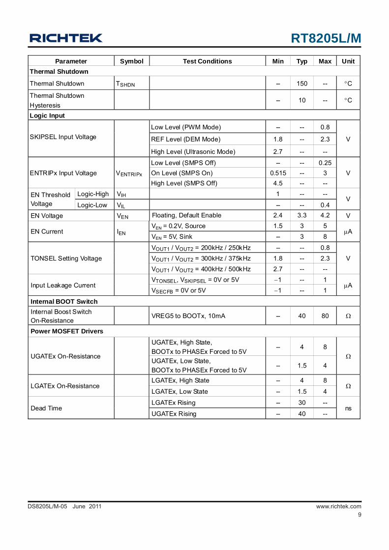
Parameter Symbol Test Conditions Min Typ Max Unit Thermal Shutdown
Thermal Shutdown TSHDN -- 150 -- °C
Thermal Shutdown Hysteresis
-- 10 -- °C
Logic Input
Low Level (PWM Mode) -- -- 0.8
REF Level (DEM Mode) 1.8 -- 2.3 SKIPSEL Input Voltage
High Level (Ultrasonic Mode) 2.7 -- --
V
Low Level (SMPS Off) -- -- 0.25 On Level (SMPS On) 0.515 -- 3 ENTRIPx Input Voltage VENTRIPx High Level (SMPS Off) 4.5 -- --
V
Logic-High VIH 1 -- -- EN Threshold Voltage Logic-Low VIL -- -- 0.4
V
EN Voltage VEN Floating, Default Enable 2.4 3.3 4.2 V VEN = 0.2V, Source 1.5 3 5
EN Current IEN VEN = 5V, Sink -- 3 8
μA
VOUT1 / VOUT2 = 200kHz / 250kHz -- -- 0.8 VOUT1 / VOUT2 = 300kHz / 375kHz 1.8 -- 2.3 TONSEL Setting Voltage VOUT1 / VOUT2 = 400kHz / 500kHz 2.7 -- --
V
VTONSEL, VSKIPSEL = 0V or 5V −1 -- 1 Input Leakage Current
VSECFB = 0V or 5V −1 -- 1 μA
Internal BOOT Switch Internal Boost Switch On-Resistance
VREG5 to BOOTx, 10mA -- 40 80 Ω
Power MOSFET Drivers UGATEx, High State, BOOTx to PHASEx Forced to 5V
-- 4 8 UGATEx On-Resistance
UGATEx, Low State, BOOTx to PHASEx Forced to 5V
-- 1.5 4 Ω
LGATEx, High State -- 4 8 LGATEx On-Resistance
LGATEx, Low State -- 1.5 4 Ω
LGATEx Rising -- 30 -- Dead Time
UGATEx Rising -- 40 -- ns

RT8205L/M
10DS8205L/M-05 June 2011www.richtek.com
Note 1. Stresses listed as the above “Absolute Maximum Ratings” may cause permanent damage to the device. These are for
stress ratings. Functional operation of the device at these or any other conditions beyond those indicated in the
operational sections of the specifications is not implied. Exposure to absolute maximum rating conditions for extended
periods may remain possibility to affect device reliability.
Note 2. θJA is measured in natural convection at TA = 25°C on a high effective four layers thermal conductivity four-layer test
board of JEDEC 51-7 thermal measurement standard. The measurement case position of θJC is on the exposed pad
of the package.
Note 3. Devices are ESD sensitive. Handling precaution is recommended.
Note 4. The device is not guaranteed to function outside its operating conditions.
Note 5. PVIN + PVREG5
Note 6. Guaranteed by Design.
RT8205L/M
11DS8205L/M-05 June 2011 www.richtek.com
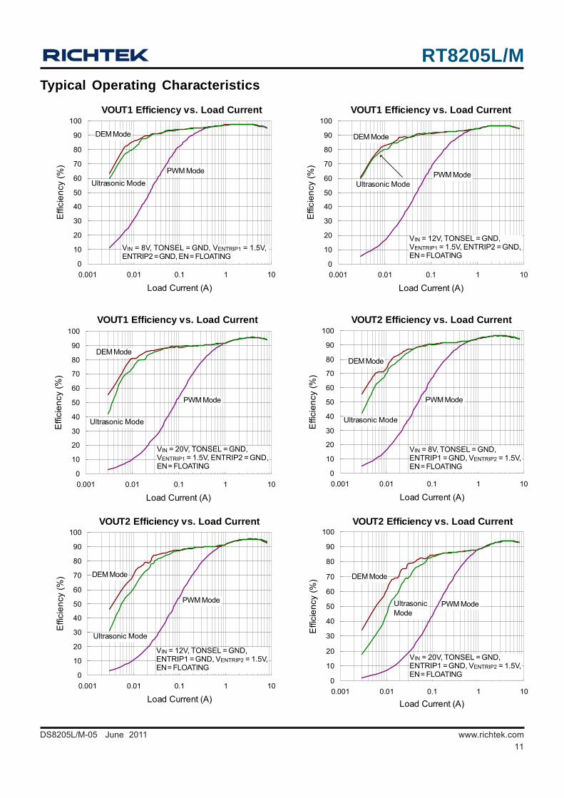
Typical Operating Characteristics
VOUT1 Efficiency vs. Load Current
0
10
20
30
40
50
60
70
80
90
100
0.001 0.01 0.1 1 10
Load Current (A)
Effi
cien
cy (%
)
VIN = 8V, TONSEL = GND, VENTRIP1 = 1.5V,ENTRIP2 = GND, EN = FLOATING
DEM Mode
Ultrasonic ModePWM Mode
VOUT1 Efficiency vs. Load Current
0
10
20
30
40
50
60
70
80
90
100
0.001 0.01 0.1 1 10
Load Current (A)
Effi
cien
cy (%
)
VIN = 12V, TONSEL = GND,VENTRIP1 = 1.5V, ENTRIP2 = GND,EN = FLOATING
DEM Mode
Ultrasonic ModePWM Mode
VOUT1 Efficiency vs. Load Current
0
10
20
30
40
50
60
70
80
90
100
0.001 0.01 0.1 1 10
Load Current (A)
Effi
cien
cy (%
)
VIN = 20V, TONSEL = GND,VENTRIP1 = 1.5V, ENTRIP2 = GND,EN = FLOATING
DEM Mode
Ultrasonic Mode
PWM Mode
VOUT2 Efficiency vs. Load Current
0
10
20
30
40
50
60
70
80
90
100
0.001 0.01 0.1 1 10
Load Current (A)
Effi
cien
cy (%
)
VIN = 8V, TONSEL = GND,ENTRIP1 = GND, VENTRIP2 = 1.5V,EN = FLOATING
DEM Mode
Ultrasonic Mode
PWM Mode
VOUT2 Efficiency vs. Load Current
0
10
20
30
40
50
60
70
80
90
100
0.001 0.01 0.1 1 10
Load Current (A)
Effi
cien
cy (%
)
VIN = 12V, TONSEL = GND,ENTRIP1 = GND, VENTRIP2 = 1.5V,EN = FLOATING
DEM Mode
Ultrasonic Mode
PWM Mode
VOUT2 Efficiency vs. Load Current
0
10
20
30
40
50
60
70
80
90
100
0.001 0.01 0.1 1 10
Load Current (A)
Effi
cien
cy (%
)
VIN = 20V, TONSEL = GND,ENTRIP1 = GND, VENTRIP2 = 1.5V,EN = FLOATING
DEM Mode
UltrasonicMode
PWM Mode
RT8205L/M
12DS8205L/M-05 June 2011www.richtek.com
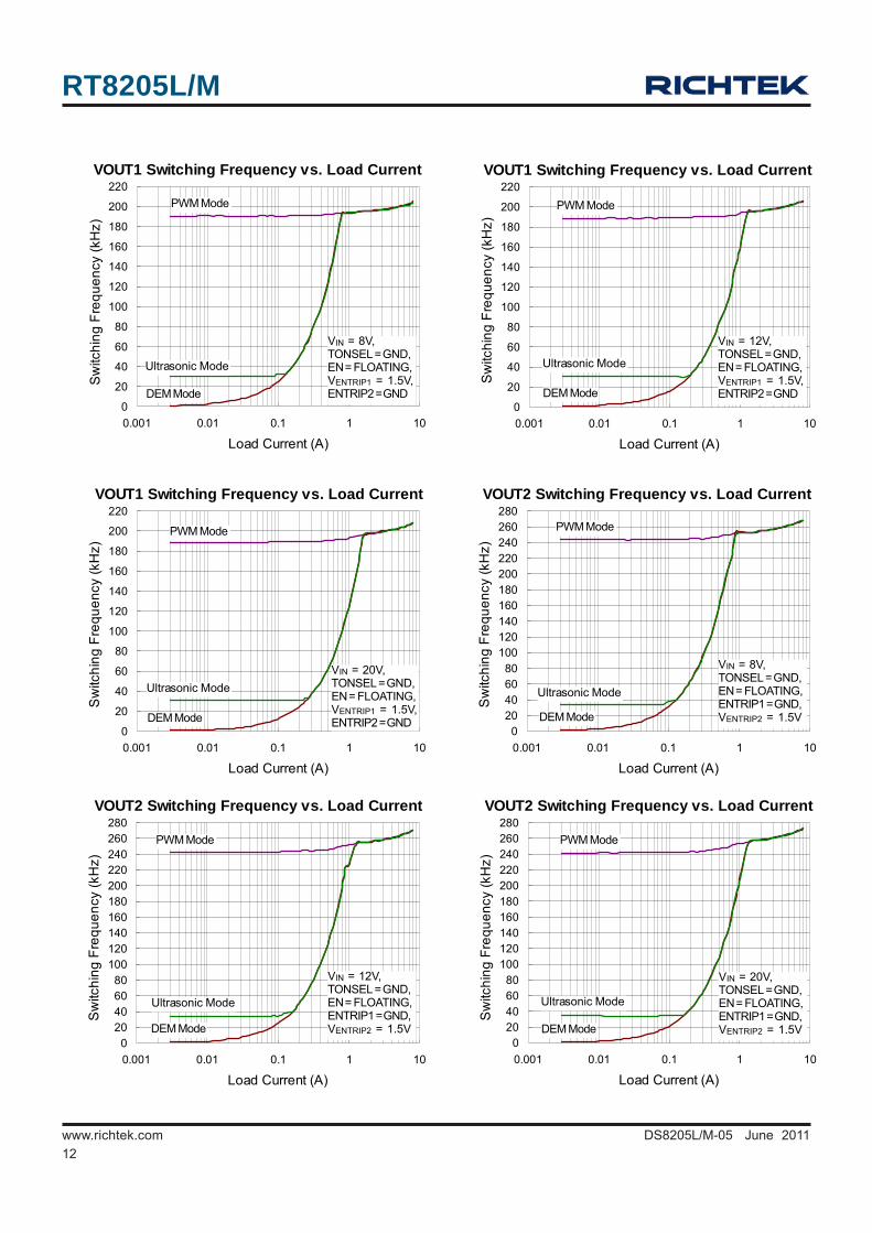
VOUT2 Switching Frequency vs. Load Current
020406080
100120140160180200220240260280
0.001 0.01 0.1 1 10
Load Current (A)
Sw
itchi
ng F
requ
ency
(kH
z) 1
VIN = 20V,TONSEL = GND,EN = FLOATING,ENTRIP1 = GND,VENTRIP2 = 1.5VDEM Mode
Ultrasonic Mode
PWM Mode
VOUT2 Switching Frequency vs. Load Current
020406080
100120140160180200220240260280
0.001 0.01 0.1 1 10
Load Current (A)
Sw
itchi
ng F
requ
ency
(kH
z) 1
VIN = 12V,TONSEL = GND,EN = FLOATING,ENTRIP1 = GND,VENTRIP2 = 1.5VDEM Mode
Ultrasonic Mode
PWM Mode
VOUT2 Switching Frequency vs. Load Current
020406080
100120140160180200220240260280
0.001 0.01 0.1 1 10
Load Current (A)
Sw
itchi
ng F
requ
ency
(kH
z) 1
VIN = 8V,TONSEL = GND,EN = FLOATING,ENTRIP1 = GND,VENTRIP2 = 1.5VDEM Mode
Ultrasonic Mode
PWM Mode
VOUT1 Switching Frequency vs. Load Current
0
20
40
60
80
100
120
140
160
180
200
220
0.001 0.01 0.1 1 10
Load Current (A)
Sw
itchi
ng F
requ
ency
(kH
z) 1
VIN = 12V,TONSEL = GND,EN = FLOATING,VENTRIP1 = 1.5V,ENTRIP2 = GNDDEM Mode
Ultrasonic Mode
PWM Mode
VOUT1 Switching Frequency vs. Load Current
0
20
40
60
80
100
120
140
160
180
200
220
0.001 0.01 0.1 1 10
Load Current (A)
Sw
itchi
ng F
requ
ency
(kH
z) 1
VIN = 8V,TONSEL = GND,EN = FLOATING,VENTRIP1 = 1.5V,ENTRIP2 = GNDDEM Mode
Ultrasonic Mode
PWM Mode
VOUT1 Switching Frequency vs. Load Current
0
20
40
60
80
100
120
140
160
180
200
220
0.001 0.01 0.1 1 10
Load Current (A)
Sw
itchi
ng F
requ
ency
(kH
z) 1
VIN = 20V,TONSEL = GND,EN = FLOATING,VENTRIP1 = 1.5V,ENTRIP2 = GNDDEM Mode
Ultrasonic Mode
PWM Mode
RT8205L/M
13DS8205L/M-05 June 2011 www.richtek.com
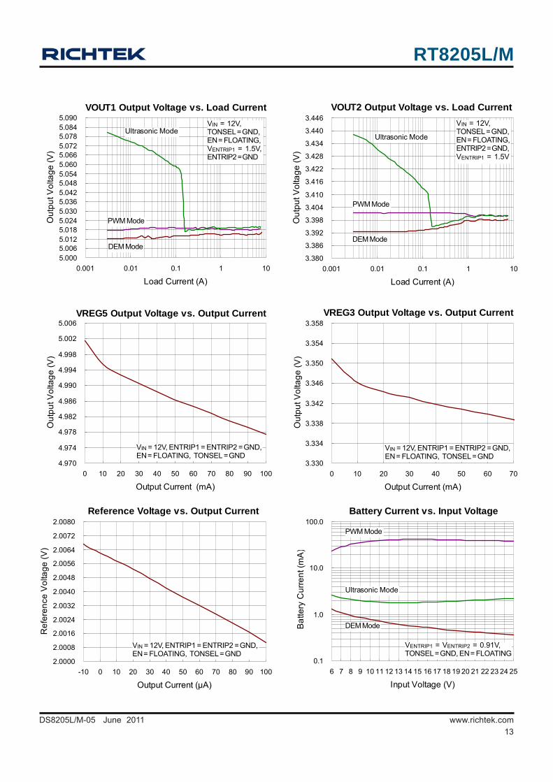
VOUT1 Output Voltage vs. Load Current
5.0005.0065.0125.0185.0245.0305.0365.0425.0485.0545.0605.0665.0725.0785.0845.090
0.001 0.01 0.1 1 10
Load Current (A)
Out
put V
olta
ge (V
)
VIN = 12V,TONSEL = GND,EN = FLOATING,VENTRIP1 = 1.5V,ENTRIP2 = GND
DEM Mode
Ultrasonic Mode
PWM Mode
VOUT2 Output Voltage vs. Load Current
3.380
3.386
3.392
3.398
3.404
3.410
3.416
3.422
3.428
3.434
3.440
3.446
0.001 0.01 0.1 1 10
Load Current (A)O
utpu
t Vol
tage
(V)
VIN = 12V,TONSEL = GND,EN = FLOATING,ENTRIP2 = GND,VENTRIP1 = 1.5V
DEM Mode
Ultrasonic Mode
PWM Mode
VREG5 Output Voltage vs. Output Current
4.970
4.974
4.978
4.982
4.986
4.990
4.994
4.998
5.002
5.006
0 10 20 30 40 50 60 70 80 90 100
Output Current (mA)
Out
put V
olta
ge (V
)
VIN = 12V, ENTRIP1 = ENTRIP2 = GND,EN = FLOATING, TONSEL = GND
VREG3 Output Voltage vs. Output Current
3.330
3.334
3.338
3.342
3.346
3.350
3.354
3.358
0 10 20 30 40 50 60 70
Output Current (mA)
Out
put V
olta
ge (V
)
VIN = 12V, ENTRIP1 = ENTRIP2 = GND,EN = FLOATING, TONSEL = GND
Reference Voltage vs. Output Current
2.0000
2.0008
2.0016
2.0024
2.0032
2.0040
2.0048
2.0056
2.0064
2.0072
2.0080
-10 0 10 20 30 40 50 60 70 80 90 100
Output Current (μA)
Ref
eren
ce V
olta
ge (V
)
VIN = 12V, ENTRIP1 = ENTRIP2 = GND,EN = FLOATING, TONSEL = GND
Battery Current vs. Input Voltage
0.1
1.0
10.0
100.0
6 7 8 9 10 11 12 13 14 15 16 17 18 19 20 21 22 23 24 25
Input Voltage (V)
Bat
tery
Cur
rent
(mA
)
VENTRIP1 = VENTRIP2 = 0.91V,TONSEL = GND, EN = FLOATING
DEM Mode
Ultrasonic Mode
PWM Mode
RT8205L/M
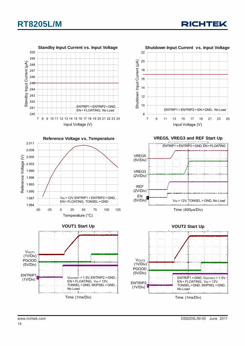
14DS8205L/M-05 June 2011www.richtek.com
Time (1ms/Div)
VOUT2 Start Up
ENTRIP1 = GND, VENTRIP2 = 1.5V,EN = FLOATING, VIN = 12V,TONSEL = GND, SKIPSEL = GND,No Load
VOUT2(1V/Div)PGOOD(5V/Div)
ENTRIP2(1V/Div)
Time (400μs/Div)
VREG5, VREG3 and REF Start Up
VIN = 12V, TONSEL = GND, No Load
ENTRIP1 = ENTRIP2 = GND, EN = FLOATING
VREG5(5V/Div)
VREG3(2V/Div)
REF(2V/Div)
EN(5V/Div)
Reference Voltage vs. Temperature
1.984
1.987
1.990
1.993
1.996
1.999
2.002
2.005
2.008
2.011
-50 -25 0 25 50 75 100 125
Temperature (°C)
Ref
eren
ce V
olta
ge (V
)
VIN = 12V, ENTRIP1 = ENTRIP2 = GND,EN = FLOATING, TONSEL = GND
Standby Input Current vs. Input Voltage
240
241
242
243
244
245
246
247
248
249
250
7 8 9 10 11 12 13 14 15 16 17 18 19 20 21 22 23 24
Input Voltage (V)
Sta
ndby
Inpu
t Cur
rent
(μA
) 1
ENTRIP1 = ENTRIP2 = GND,EN = FLOATING, No Load
Shutdown Input Current vs. Input Voltage
8
10
12
14
16
18
20
22
7 9 11 13 15 17 19 21 23 25
Input Voltage (V)
Shu
tdow
n In
put C
urre
nt (μ
A) 1
ENTRIP1 = ENTRIP2 = EN = GND, No Load
Time (1ms/Div)
VOUT1 Start Up
VENTRIP1 = 1.5V, ENTRIP2 = GND,EN = FLOATING, VIN = 12V,TONSEL = GND, SKIPSEL = GND,No Load
VOUT1(1V/Div)PGOOD(5V/Div)
ENTRIP1(1V/Div)
RT8205L/M
15DS8205L/M-05 June 2011 www.richtek.com
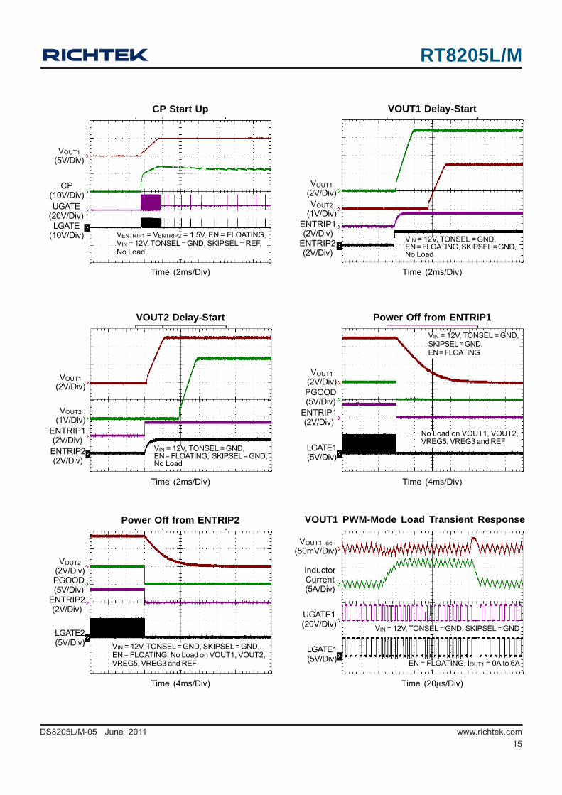
Time (4ms/Div)
Power Off from ENTRIP2
VIN = 12V, TONSEL = GND, SKIPSEL = GND,EN = FLOATING, No Load on VOUT1, VOUT2,VREG5, VREG3 and REF
VOUT2(2V/Div)
ENTRIP2(2V/Div)
LGATE2(5V/Div)
PGOOD(5V/Div)
Time (4ms/Div)
Power Off from ENTRIP1
VIN = 12V, TONSEL = GND,SKIPSEL = GND,EN = FLOATING
No Load on VOUT1, VOUT2,VREG5, VREG3 and REF
VOUT1(2V/Div)
ENTRIP1(2V/Div)
LGATE1(5V/Div)
PGOOD(5V/Div)
Time (2ms/Div)
VOUT1 Delay-Start
VIN = 12V, TONSEL = GND,EN = FLOATING, SKIPSEL = GND,No Load
VOUT1(2V/Div)
ENTRIP1(2V/Div)
ENTRIP2(2V/Div)
VOUT2(1V/Div)
Time (2ms/Div)
VOUT2 Delay-Start
VIN = 12V, TONSEL = GND,EN = FLOATING, SKIPSEL = GND,No Load
VOUT1(2V/Div)
ENTRIP1(2V/Div)
ENTRIP2(2V/Div)
VOUT2(1V/Div)
Time (2ms/Div)
CP Start Up
VENTRIP1 = VENTRIP2 = 1.5V, EN = FLOATING,VIN = 12V, TONSEL = GND, SKIPSEL = REF,No Load
VOUT1(5V/Div)
UGATE(20V/Div)LGATE
(10V/Div)
CP(10V/Div)
Time (20μs/Div)
VOUT1 PWM-Mode Load Transient Response
EN = FLOATING, IOUT1 = 0A to 6A
VIN = 12V, TONSEL = GND, SKIPSEL = GND
VOUT1_ac(50mV/Div)
UGATE1(20V/Div)
LGATE1(5V/Div)
InductorCurrent(5A/Div)
RT8205L/M
16DS8205L/M-05 June 2011www.richtek.com
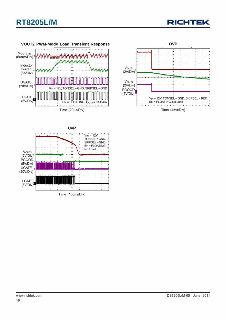
Time (4ms/Div)
OVP
VIN = 12V, TONSEL = GND, SKIPSEL = REF,EN = FLOATING, No Load
VOUT1(2V/Div)
PGOOD(5V/Div)
VOUT2(2V/Div)
Time (100μs/Div)
UVP
VIN = 12V,TONSEL = GND,SKIPSEL = GND,EN = FLOATING,No Load
VOUT1(2V/Div)
UGATE(20V/Div)
LGATE(5V/Div)
PGOOD(5V/Div)
Time (20μs/Div)
VOUT2 PWM-Mode Load Transient Response
EN = FLOATING, IOUT2 = 0A to 6A
VIN = 12V, TONSEL = GND, SKIPSEL = GND
VOUT2_ac(50mV/Div)
UGATE(20V/Div)
LGATE(5V/Div)
InductorCurrent(5A/Div)
RT8205L/M
17DS8205L/M-05 June 2011 www.richtek.com
Application InformationThe RT8205L/M is a dual, Mach ResponseTM DRVTM dualramp valley mode synchronous buck controller. Thecontroller is designed for low-voltage power supplies fornotebook computers. Richtek's Mach ResponseTM
technology is specifically designed for providing 100ns“instant-on” response to load steps while maintaining arelatively constant operating frequency and inductoroperating point over a wide range of input voltages. Thetopology circumvents the poor load-transient timingproblems of fixed-frequency current-mode PWMs whileavoiding the problems caused by widely varying switchingfrequencies in conventional constant-on-time and constant-off-time PWM schemes. The DRVTM mode PWMmodulator is specifically designed to have better noiseimmunity for such a dual output application. The RT8205L/M includes 5V (VREG5) and 3.3V (VREG3) linearregulators. VREG5 linear regulator can step down thebattery voltage to supply both internal circuitry and gatedrivers. The synchronous-switch gate drivers are directlypowered from VREG5. When VOUT1 voltage is above4.66V, an automatic circuit will switch the power of thedevice from VREG5 linear regulator to VOUT1.
PWM OperationThe Mach ResponseTM DRVTM mode controller relies onthe output filter capacitor's Effective Series Resistance(ESR) to act as a current-sense resistor, so the outputripple voltage provides the PWM ramp signal. Referring tothe RT8205L/M's function block diagram, the synchronoushigh side MOSFET will be turned on at the beginning ofeach cycle. After the internal one-shot timer expires, theMOSFET will be turned off. The pulse width of this oneshot is determined by the converter's input voltage andthe output voltage to keep the frequency fairly constantover the input voltage range. Another one-shot sets aminimum off-time (300ns typ.). The on-time one-shot willbe triggered if the error comparator is high, the low sideswitch current is below the current limit threshold, andthe minimum off-time one-shot has timed out.
PWM Frequency and On-Time ControlThe Mach ResponseTM control architecture runs withpseudo constant frequency by feed forwarding the input
and output voltage into the on-time one shot timer. Thehigh side switch on-time is inversely proportional to theinput voltage as measured by VIN, and proportional to theoutput voltage. There are two benefits of a constantswitching frequency. First, the frequency can be selectedto avoid noise-sensitive regions such as the 455kHz IFband. Second, the inductor ripple-current operating pointremains relatively constant, resulting in easy designmethodology and predictable output voltage ripple.Frequency for the 3V SMPS is set at 1.25 times higherthan the frequency for 5V SMPS. This is done to preventaudio frequency “beating” between the two sides, whichswitches asynchronously for each side. The frequenciesare set by the TONSEL pin connection as shown in Table1. The on-time is given by :
/ON OUT INt K (V V )= ×
where “K” is set by the TONSEL pin connection (Table1).
The on-time guaranteed in the Electrical Characteristicstable is influenced by switching delays in the externalhigh side power MOSFET. Two external factors thatinfluence switching frequency accuracy are resistive dropsin the two conduction loops (including inductor and PCboard resistance) and the dead time effect. These effectsare the largest contributors to the change frequency withchanging load current. The dead time effect increases theeffective on-time by reducing the switching frequency. Itoccurs only in PWM mode (SKIPSEL = GND) when theinductor current reverses at light or negative load currents.With reversed inductor current, the inductor's EMF causesPHASEx to go high earlier than normal, thus extendingthe on-time by a period equal to the low-to-high dead time.For loads above the critical conduction point, the actualswitching frequency is :
/OUT DROP1 ON IN DROP1 DROP2f (V V ) (t (V V V ))= + × + −
where VDROP1 is the sum of the parasitic voltage drops inthe inductor discharge path, which includes thesynchronous rectifier, inductor, and PC board resistances.VDROP2 is the sum of the resistances in the charging path;and tON is the on-time.
RT8205L/M
18DS8205L/M-05 June 2011www.richtek.com
Table 1. TONSEL Connection and Switching Frequency
TONSEL SMPS 1 K-Factor (μs)
SMPS 1 Frequency (kHz)
SMPS 2 K-Factor (μs)
SMPS 2 Frequency (kHz)
Approximate K-Factor Error (%)
GND 5 200 4 250 ±10
REF 3.33 300 2.67 375 ±10 VREG5 or
VREG3 2.5 400 2 500 ±10
Operation Mode Selection (SKIPSEL)The RT8205L/M supports three operation modes: Diode-Emulation Mode, Ultrasonic Mode, and Forced-CCMMode. User can set operation mode via the SKIPSEL pin.
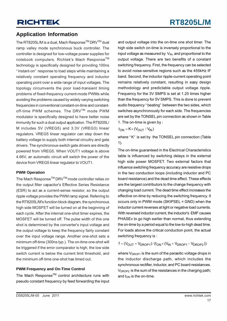
Diode-Emulation Mode (SKIPSEL = REF)In Diode-Emulation Mode, the RT8205L/M automaticallyreduces switching frequency at light load conditions tomaintain high efficiency. This reduction of frequency isachieved smoothly. As the output current decreases fromheavy load condition, the inductor current is also reducedand eventually comes to the point when its valley toucheszero current, which is the boundary between continuousconduction and discontinuous conduction modes. Byemulating the behavior of diodes, the low side MOSFETallows only partial negative current when the inductor freewheeling current becomes negative. As the load currentis further decreased, it takes longer and longer to dischargethe output capacitor to the level that requires the next“ON” cycle. The on-time is kept the same as that in theheavy-load condition. In reverse, when the output currentincreases from light load to heavy load, the switchingfrequency increases to the preset value as the inductorcurrent reaches the continuous conduction. The transitionload point to the light load operation as follows (Figure 1) :
Figure 1. Boundary Condition of CCM/DEM
IN OUTLOAD(SKIP) ON
(V V )I t
2L−
≈ ×
where tON is the On-time.
The switching waveforms may appear noisy andasynchronous when light loading causes Diode-EmulationMode operation. However, this is normal and results inhigh efficiency. Trade offs in PFM noise vs. light loadefficiency is made by varying the inductor value. Generally,low inductor values produce a broader efficiency vs. loadcurve, while higher values result in higher full load efficiency(assuming that the coil resistance remains fixed) and lessoutput voltage ripple. Penalties for using higher inductorvalues include larger physical size and degraded loadtransient response (especially at low input voltage levels).
Ultrasonic Mode (SKIPSEL = VREG5 or VREG3)The RT8205L/M activates an unique Diode-Emulation Modewith a minimum switching frequency of 25kHz, called theUltrasonic Mode. The Ultrasonic Mode avoids audio-frequency modulation that would otherwise be presentwhen a lightly loaded controller automatically skipspulses. In Ultrasonic Mode, the high side switch gate driversignal is ORed with an internal oscillator (>25kHz). Oncethe internal oscillator is triggered, the controller entersconstant off-time control. When output voltage reachesthe setting peak threshold, the controller turns on the lowside MOSFET until the controller detects that the inductorcurrent has dropped below the zero crossing threshold.The internal circuitry provides a constant off-time control,and it is effective to regulate the output voltage under lightload condition.
Forced CCM Mode (SKIPSEL = GND)The low noise, Forced CCM mode (SKIPSEL = GND)disables the zero crossing comparator, which controlsthe low side switch on-time. This causes the low side
IL
t0 tON
Slope = (VIN -VOUT) / LIL, PEAK
ILoad = IL, PEAK / 2
RT8205L/M
19DS8205L/M-05 June 2011 www.richtek.com
ILIMx ILIMx ILIMx DS(ON)V (R 10 A)/10 I Rμ= × = ×
/ILIMx ILIMx DS(ON)R (I R ) 10 10 Aμ= × ×
Carefully observe the PC board layout guidelines toensures that noise and DC errors do not corrupt the currentsense signal at PHASEx and GND. Mount or place the ICclose to the low side MOSFET.
Charge Pump (SECFB)The external 14V charge pump is driven by LGATEx (Figure3). When LGATEx is low, C1 will be charged by D1 fromVOUT1. C1 voltage is equal to VOUT1 minus a diode drop.When LGATEx transitions to high, the charges from C1will transfer to C2 through D2 and charge it to VLGATEX plusVC1. As LGATEx transitions low on the next cycle, C2will charge C3 to its voltage minus a diode drop through
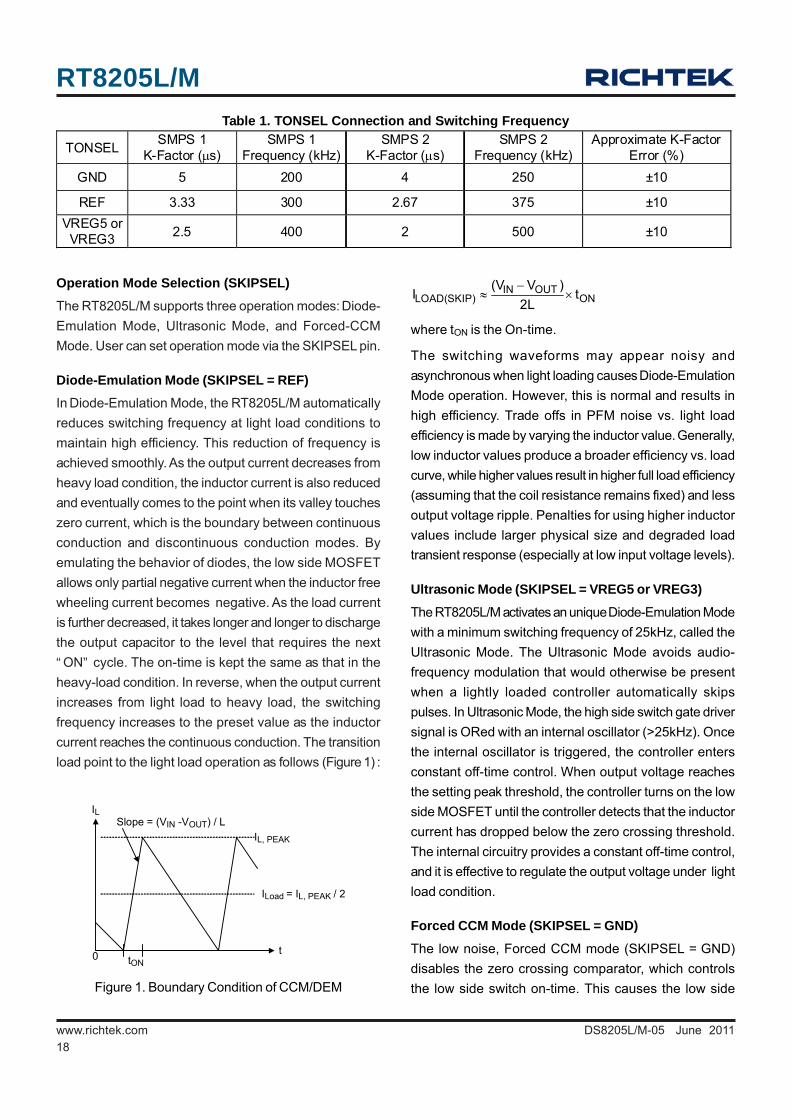
Figure 2. “ Valley” Current Limit
The RT8205L/M uses the on resistance of the synchronousrectifier as the current sense element and supportstemperature compensated MOSFET RDS(ON) sensing. TheRILIMx resistor between the ENTRIPx pin and GND setsthe current limit threshold. The resistor RILIMx is connectedto a current source from ENTRIPx, which is typically10μAat room temperature. The current source has a 4700ppm/°C temperature slope to compensate the temperaturedependency of the RDS(ON). When the voltage drop acrossthe sense resistor or low side MOSFET equals 1/10 thevoltage across the RILIMx resistor, positive current limitwill be activated. The high side MOSFET will not be turnedon until the voltage drop across the MOSFET falls below1/10 the voltage across the RILIMx resistor.
Choose a current limit resistor by following equation :
gate driver waveform to become the complement of thehigh side gate driver waveform. This in turn causes theinductor current to reverse at light loads as the PWM loopto maintain a duty ratio of VOUT/VIN. The benefit of forcedCCM mode is to keep the switching frequency fairlyconstant, but it comes at a cost. The no-load batterycurrent can be from 10mA to 40mA, depending on theexternal MOSFETs.
Reference and Linear Regulators (REF, VREGx)The 2V reference (REF) is accurate within ±1% over theentire operating temperature range, making REF usefulas a precision system reference. Bypass REF to GNDwith a minimum 0.22μF ceramic capacitor. REF can supplyup to 100μA for external loads. Loading REF reduces theVOUTx output voltage slightly because of the referenceload regulation error.
The RT8205L/M includes 5V (VREG5) and 3.3V (VREG3)linear regulators. The VREG5 regulator supplies a total of100mA for internal and external loads, including theMOSFET gate driver and PWM controller. The VREG3regulator supplies up to 100mA for external loads. BypassVREG5 and VREG3 with a minimum 4.7μF ceramiccapacitor.
When the 5V main output voltage is above the VREG5switchover threshold (4.75V), an internal 1.5Ω P- MOSFETswitch connects VOUT1 to VREG5, while simultaneouslyshutting down the VREG5 linear regulator. Similarly, whenthe 3.3V main output voltage is above the VREG3switchover threshold (3.125V), an internal 1.5ΩP-MOSFET switch connects VOUT2 to VREG3, whilesimultaneously shutting down the VREG3 linear regulator.It can decrease the power dissipation from the samebattery, because the converted efficiency of SMPS isbetter than the converted efficiency of the linear regulator.
Current Limit Setting (ENTRIPx)The RT8205L/M has a cycle-by-cycle current limit control.The current limit circuit employs an unique “Valley” currentsensing algorithm. If the magnitude of the current sensesignal at PHASEx is above the current limit threshold,the PWM is not allowed to initiate a new cycle (Figure 2).The actual peak current is greater than the current limitthreshold by an amount equal to the inductor ripple current.
Therefore, the exact current limit characteristic andmaximum load capability are functions of the senseresistance, inductor value, and battery and output voltage.
IL
t0
IL, peak
ILIM
ILoad
RT8205L/M
20DS8205L/M-05 June 2011www.richtek.com
CP LGATEX DV VOUT1 2 V 4 V= + × − ×
where VLGATEX is the peak voltage of LGATEx driver and isequal to the VREG5; VD is the forward diode droppedacross the Schottky.
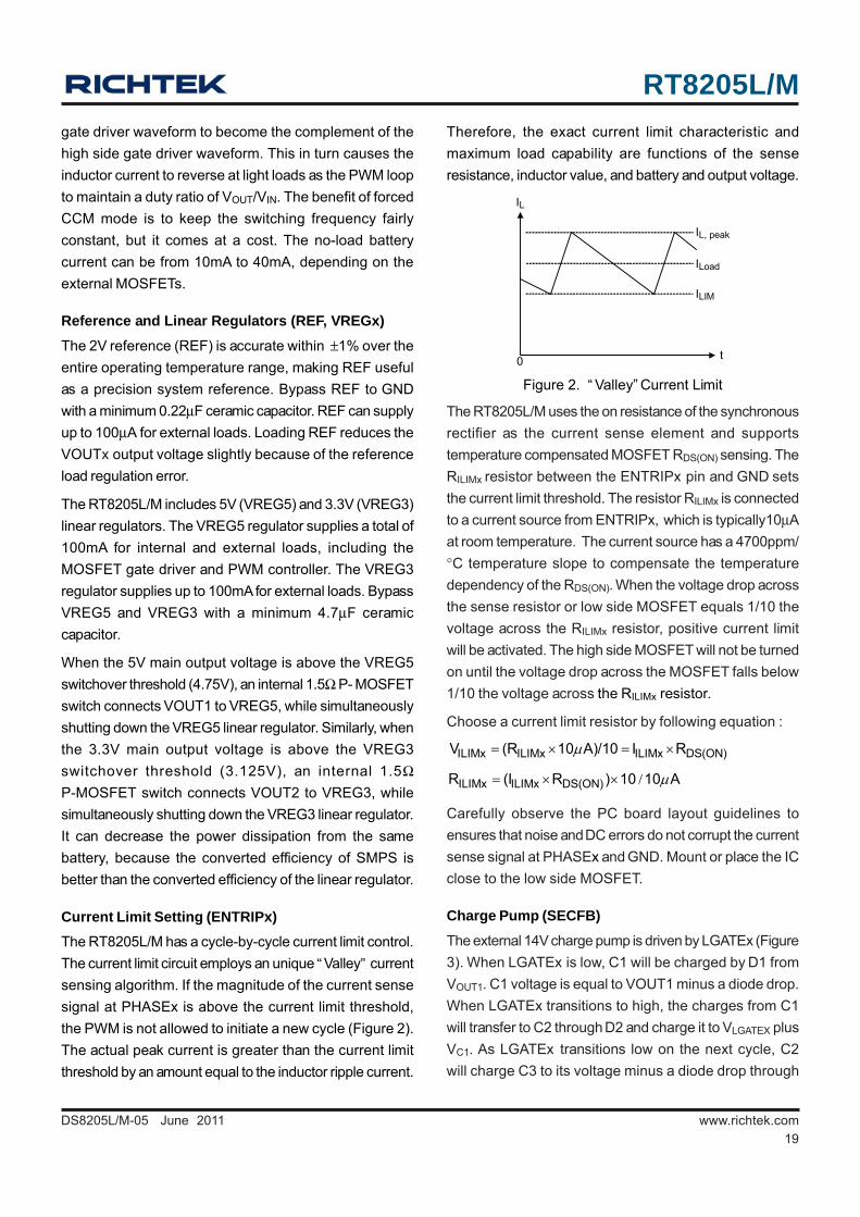
SECFB in the RT8205M is used to monitor the chargepump through the resistive divider (Figure 3) to generateapproximately 14V DC voltage and the clock driver usesVOUT1 as its power supply. In the event when SECFBdrops below its feedback threshold, an ultrasonic pulsewill occur to refresh the charge pump driven by LGATEx.In the event of an overload on charge pump where SECFBcan not reach more than its feedback threshold, thecontroller will enter the ultrasonic mode. Special careshould be taken to ensure enough normal ripple voltageon each cycle as to prevent charge pump shutdown.
Reducing the charge pump decoupling capacitor andplacing a small ceramic capacitor (47 pF to 220pF) (CF ofFigure 3) in parallel with the upper leg of the SECFBresistor feedback network (RCP1 of Figure 3) will alsoincrease the robustness of the charge pump.
Figure 3. Charge Pump Circuit Connected to SECFB
MOSFET Gate Driver (UGATEx, LGATEx)
The high side driver is designed to drive high current, lowRDS(ON) N-MOSFET(s). When configured as a floating driver,a 5V bias voltage is delivered from the VREG5 supply.The average drive current is calculated by the gate chargeat VGS = 5V times the switching frequency. Theinstantaneous drive current is supplied by the flyingcapacitor between the BOOTx and PHASEx pins. A deadtime to prevent shoot through is internally generatedbetween the high side MOSFET off to, the low sideMOSFET on, and the low side MOSFET off to the highside MOSFET on.
Figure 4. Reducing the UGATEx Rise Time
D3. Finally, C3 charges C4 through D4 when LGATExswitches to high. So, VCP voltage is :
The low side driver is designed to drive high current, lowRDS(ON) N-MOSFET(s). The internal pull down transistorthat drives LGATEx low is robust, with a 1.5Ω typical onresistance. A 5V bias voltage is delivered from the VREG5supply. The instantaneous drive current is supplied by aninput capacitor connected between VREG5 and GND.
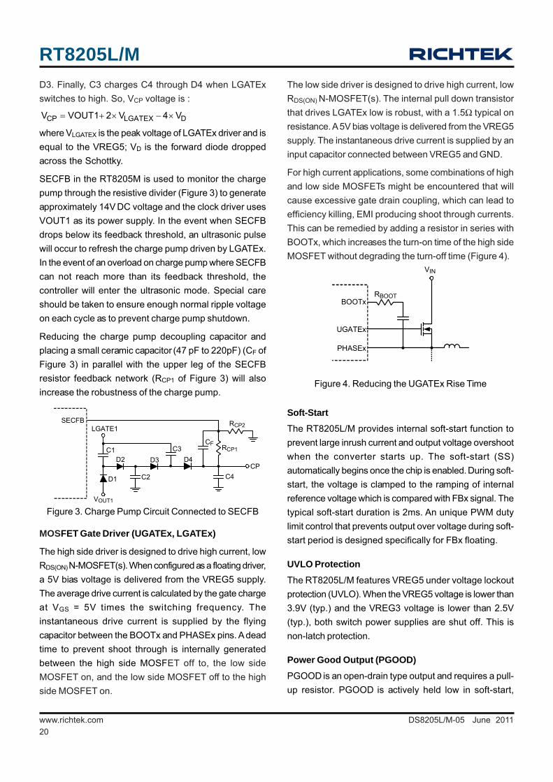
For high current applications, some combinations of highand low side MOSFETs might be encountered that willcause excessive gate drain coupling, which can lead toefficiency killing, EMI producing shoot through currents.This can be remedied by adding a resistor in series withBOOTx, which increases the turn-on time of the high sideMOSFET without degrading the turn-off time (Figure 4).
Soft-StartThe RT8205L/M provides internal soft-start function toprevent large inrush current and output voltage overshootwhen the converter starts up. The soft-start (SS)automatically begins once the chip is enabled. During soft-start, the voltage is clamped to the ramping of internalreference voltage which is compared with FBx signal. Thetypical soft-start duration is 2ms. An unique PWM dutylimit control that prevents output over voltage during soft-start period is designed specifically for FBx floating.
UVLO ProtectionThe RT8205L/M features VREG5 under voltage lockoutprotection (UVLO). When the VREG5 voltage is lower than3.9V (typ.) and the VREG3 voltage is lower than 2.5V(typ.), both switch power supplies are shut off. This isnon-latch protection.
Power Good Output (PGOOD)PGOOD is an open-drain type output and requires a pull-up resistor. PGOOD is actively held low in soft-start,
BOOTx
UGATEx
PHASEx
RBOOT
VIN
SECFB
VOUT1
C1
C2
C3
C4D1
D2 D3 D4CP
RCP1CF
RCP2LGATE1
RT8205L/M
21DS8205L/M-05 June 2011 www.richtek.com
standby, and shutdown. It is released when both outputvoltages are above 91% of the nominal regulation point.The PGOOD goes low if either output turns off or is 15%below its nominal regulator point.
Output Over Voltage Protection (OVP)The output voltage can be continuously monitored for overvoltage. If the output voltage exceeds 12% of its set voltagethreshold, the over voltage protection is triggered and theLGATEx low side gate drivers are forced high. Thisactivates the low side MOSFET switch, which rapidlydischarges the output capacitor and pulls the input voltagedownward.
The RT8205L/M is latched once OVP is triggered and canonly be released by toggling EN, ENTRIPx or cycling VIN.There is a 5μs delay built into the over voltage protectioncircuit to prevent false alarm.
Note that the latching LGATEx high causes the outputvoltage to dip slightly negative when energy has beenpreviously stored in the LC tank circuit. For loads thatcannot tolerate a negative voltage, place a power Schottkydiode across the output to act as a reverse polarity clamp.
If the over voltage condition is caused by a short in thehigh side switch, completely turning on the low sideMOSFET can create an electrical short between thebattery and GND, which will blow the fuse and disconnectthe battery from the output.
Output Under Voltage Protection (UVP)The output voltage can be continuously monitored for undervoltage protection. If the output is less than 52% of its setvoltage threshold, under voltage protection will be triggered,and then both UGATEx and LGATEx gate drivers will beforced low. The UVP will be ignored for at least 5ms (typ.)after start up or a rising edge on ENTRIPx. Toggle ENTRIPxor cycle VIN to reset the UVP fault latch and restart thecontroller.
Thermal ProtectionThe RT8205L/M features thermal shutdown protection toprevent overheat damage to the device. Thermal shutdownoccurs when the die temperature exceeds 150°C. Allinternal circuitry is inactive during thermal shutdown. TheRT8205L/M triggers thermal shutdown if VREGx is not
supplied from VOUTx, while the input voltage on VIN andthe drawing current from VREGx are too high. Even ifVREGx is supplied from VOUTx, large power dissipationon automatic switches caused by overloading VREGx,which may also result in thermal shutdown.
Discharge Mode (Soft-Discharge)When ENTRIPx is low and a transition to standby orshutdown mode occurs, or the output under voltage faultlatch is set, the output discharge mode will be triggered.During discharge mode, the output capacitors' residualcharge will be discharge to GND through an internal switch.
Shutdown ModeThe RT8205L/M SMPS1, SMPS2, VREG3 and VREG5have independent enabling control. Drive EN, ENTRIP1and ENTRIP2 below the precise input falling edge trip levelto place the RT8205L/M in its low power shutdown state.The RT8205L/M consumes only 20μA of input current whilein shutdown. When shutdown mode is activated, thereference turns off. The accurate 0.4V falling edge thresholdon the EN pin can be used to detect a specific analogvoltage level as well as to shutdown the device. Once inshutdown, the 1V rising edge threshold activates, providingsufficient hysteresis for most applications.
Power Up Sequencing and On/Off Controls(ENTRIPx)ENTRIP1 and ENTRIP2 control the SMPS power upsequencing. When the RT8205L/M is in single channelmode, ENTRIP1 or ENTRIP2 enables the respectiveoutputs when ENTRIPx voltage rises above 0.515V.
Since current source form ENTRIPx has 4700ppm/°Ctemperature slope, please make sure that ENTRIPx voltageis high enough to enable the respective output in lowtemperature application.
If ENTRIPx pin becomes higher than the enable thresholdvoltage while another channel is starting up, soft-start ispostponed until the other channel's soft-start hascompleted. If both ENTRIP1 and ENTRIP2 become higherthan the enable threshold voltage simultaneously (within60μs), both channels will be start up simultaneously. Thetiming diagrams of the power sequence is shown below(Figure 5).
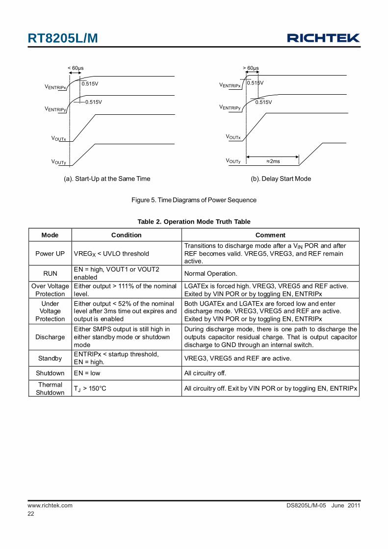
RT8205L/M
22DS8205L/M-05 June 2011www.richtek.com
(a). Start-Up at the Same Time (b). Delay Start Mode
Figure 5. Time Diagrams of Power Sequence
Table 2. Operation Mode Truth Table
Mode Condition Comment
Power UP VREGX < UVLO threshold Transitions to discharge mode after a VIN POR and after REF becomes valid. VREG5, VREG3, and REF remain active.
RUN EN = high, VOUT1 or VOUT2 enabled Normal Operation.
Over Voltage Protection
Either output > 111% of the nominal level.
LGATEx is forced high. VREG3, VREG5 and REF active. Exited by VIN POR or by toggling EN, ENTRIPx
Under Voltage
Protection
Either output < 52% of the nominal level after 3ms time out expires and output is enabled
Both UGATEx and LGATEx are forced low and enter discharge mode. VREG3, VREG5 and REF are active. Exited by VIN POR or by toggling EN, ENTRIPx
Discharge Either SMPS output is still high in either standby mode or shutdown mode
During discharge mode, there is one path to discharge the outputs capacitor residual charge. That is output capacitor discharge to GND through an internal switch.
Standby ENTRIPx < startup threshold, EN = high. VREG3, VREG5 and REF are active.
Shutdown EN = low All circuitry off.
Thermal Shutdown TJ > 150°C All circuitry off. Exit by VIN POR or by toggling EN, ENTRIPx
VENTRIPx
VENTRIPy
< 60µs
VOUTx
VOUTy
0.515V
0.515V
VOUTx
> 60µs
0.515V
0.515V
VOUTy 2ms
VENTRIPx
VENTRIPy
≈
RT8205L/M
23DS8205L/M-05 June 2011 www.richtek.com
Output Inductor SelectionThe switching frequency (on-time) and operating point (%ripple or LIR) determine the inductor value as shown inthe following equation :
ON IN OUTx
LOAD(MAX)
t (V V )L
LIR I× −
=×
where LIR is the ratio of the peak to peak ripple current tothe average inductor current.
Find a low loss inductor having the lowest possible DCresistance that fits in the allotted dimensions. Ferrite coresare often the best choice, although powdered iron isinexpensive and can work well at 200kHz. The core mustbe large enough not to saturate at the peak inductor current(IPEAK) :
/ )⎡ ⎤= + ×⎣ ⎦PEAK LOAD(MAX) LOAD(MAX)I I (LIR 2 I
The calculation above shall serve as a general reference.To further improve the transient response, the outputinductance can be reduced even further. This needs to beconsidered along with the selection of the output capacitor.
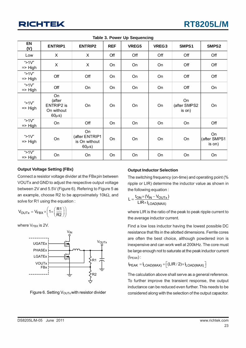
Table 3. Power Up SequencingEN (V) ENTRIP1 ENTRIP2 REF VREG5 VREG3 SMPS1 SMPS2
Low X X Off Off Off Off Off
“>1V” => High X X On On On Off Off
“>1V” => High Off Off On On On Off Off
“>1V” => High Off On On On On Off On
“>1V” => High
On (after
ENTRIP2 is On without
60μs)
On On On On On
(after SMPS2 is on)
On
“>1V” => High On Off On On On On Off
“>1V” => High On
On (after ENTRIP1 is On without
60μs)
On On On On On
(after SMPS1 is on)
“>1V” => High On On On On On On On
Output Voltage Setting (FBx)Connect a resistor voltage divider at the FBx pin betweenVOUTx and GND to adjust the respective output voltagebetween 2V and 5.5V (Figure 6). Refering to Figure 5 asan example, choose R2 to be approximately 10kΩ, andsolve for R1 using the equation :
OUTx FBXR1V V 1R2
⎛ ⎞⎛ ⎞= × +⎜ ⎟⎜ ⎟⎝ ⎠⎝ ⎠
where VFBX is 2V.
Figure 6. Setting VOUTx with resistor divider
PHASEx
LGATExR1
R2
VOUTx
VIN
UGATEx
VOUTxFBx
RT8205L/M
24DS8205L/M-05 June 2011www.richtek.com
2 OUTxLOAD OFF(MIN)
INSAG
IN OUTxOUT OUTx OFF(MIN)
IN
V( I ) L (K t )VV
V V2 C V K tV
Δ × × +=
⎡ ⎤⎛ ⎞−× × × −⎢ ⎥⎜ ⎟
⎝ ⎠⎣ ⎦2
LOADSOAR
OUT OUTx
( I ) LV
2 C VΔ ×
=× ×
P P LOAD(MAX)OUT
1V LIR I ESR8 C f−
⎛ ⎞= × × +⎜ ⎟× ×⎝ ⎠
where VSAG and VSOAR are the allowable amount ofundershoot voltage and overshoot voltage in the loadtransient, Vp-p is the output ripple voltage, tOFF(MIN) is theminimum off-time, and K is a factor listed in from Table 1.
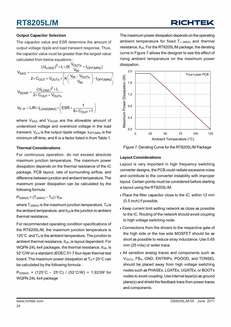
Thermal ConsiderationsFor continuous operation, do not exceed absolutemaximum junction temperature. The maximum powerdissipation depends on the thermal resistance of the ICpackage, PCB layout, rate of surrounding airflow, anddifference between junction and ambient temperature. Themaximum power dissipation can be calculated by thefollowing formula :
PD(MAX) = (TJ(MAX) − TA) / θJA
where TJ(MAX) is the maximum junction temperature, TA isthe ambient temperature, and θJA is the junction to ambientthermal resistance.
For recommended operating condition specifications ofthe RT8205L/M, the maximum junction temperature is125°C and TA is the ambient temperature. The junction toambient thermal resistance, θJA, is layout dependent. ForWQFN-24L 4x4 packages, the thermal resistance, θJA, is52°C/W on a standard JEDEC 51-7 four-layer thermal testboard. The maximum power dissipation at TA = 25°C canbe calculated by the following formula :
PD(MAX) = (125°C − 25°C) / (52°C/W) = 1.923W forWQFN-24L 4x4 package
Figure 7. Derating Curve for the RT8205L/M Package
Output Capacitor SelectionThe capacitor value and ESR determine the amount ofoutput voltage ripple and load transient response. Thus,the capacitor value must be greater than the largest valuecalculated from below equations :
Layout ConsiderationsLayout is very important in high frequency switchingconverter designs, the PCB could radiate excessive noiseand contribute to the converter instability with improperlayout. Certain points must be considered before startinga layout using the RT8205L/M.
Place the filter capacitor close to the IC, within 12 mm(0.5 inch) if possible.
Keep current limit setting network as close as possibleto the IC. Routing of the network should avoid couplingto high voltage switching node.
Connections from the drivers to the respective gate ofthe high side or the low side MOSFET should be asshort as possible to reduce stray inductance. Use 0.65mm (25 mils) or wider trace.
All sensitive analog traces and components such asVOUTx, FBX, GND, ENTRIPx, PGOOD, and TONSELshould be placed away from high voltage switchingnodes such as PHASEx, LGATEx, UGATEx, or BOOTxnodes to avoid coupling. Use internal layer(s) as groundplane(s) and shield the feedback trace from power tracesand components.
The maximum power dissipation depends on the operatingambient temperature for fixed TJ (MAX) and thermalresistance, θJA. For the RT8205L/M package, the deratingcurve in Figure 7 allows the designer to see the effect ofrising ambient temperature on the maximum powerdissipation.
0.0
0.4
0.8
1.2
1.6
2.0
0 25 50 75 100 125
Ambient Temperature (°C)
Max
imum
Pow
er D
issi
patio
n (W
) 1 Four-Layer PCB
RT8205L/M
25DS8205L/M-05 June 2011 www.richtek.com
Place the ground terminal of VIN capacitor(s), VOUTx
capacitor(s), and source of low side MOSFETs as closeas possible. The PCB trace defined as PHASEx node,which connects to source of high side MOSFET, drainof low side MOSFET and high voltage side of theinductor, should be as short and wide as possible.
RT8205L/M
26DS8205L/M-05 June 2011www.richtek.com
Information that is provided by Richtek Technology Corporation is believed to be accurate and reliable. Richtek reserves the right to make any change in circuit
design, specification or other related things if necessary without notice at any time. No third party intellectual property infringement of the applications should be
guaranteed by users when integrating Richtek products into any application. No legal responsibility for any said applications is assumed by Richtek.
Richtek Technology CorporationHeadquarter5F, No. 20, Taiyuen Street, Chupei CityHsinchu, Taiwan, R.O.C.Tel: (8863)5526789 Fax: (8863)5526611
Richtek Technology CorporationTaipei Office (Marketing)5F, No. 95, Minchiuan Road, Hsintien CityTaipei County, Taiwan, R.O.C.Tel: (8862)86672399 Fax: (8862)86672377Email: [email protected]
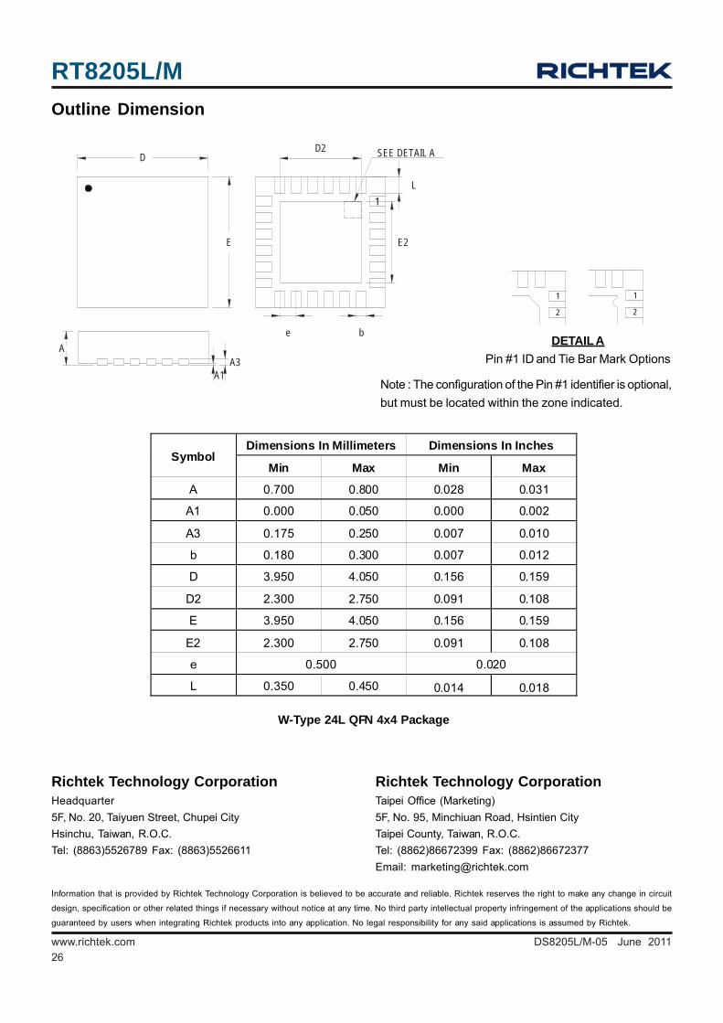
Outline Dimension
A
A1A3
D
E
D2
E2
L
be
1
SEE DETAIL A
Dimensions In Millimeters Dimensions In Inches Symbol
Min Max Min Max
A 0.700 0.800 0.028 0.031
A1 0.000 0.050 0.000 0.002
A3 0.175 0.250 0.007 0.010
b 0.180 0.300 0.007 0.012
D 3.950 4.050 0.156 0.159
D2 2.300 2.750 0.091 0.108
E 3.950 4.050 0.156 0.159
E2 2.300 2.750 0.091 0.108
e 0.500 0.020
L 0.350 0.450 0.014 0.018
W-Type 24L QFN 4x4 Package
Note : The configuration of the Pin #1 identifier is optional,but must be located within the zone indicated.
DETAIL APin #1 ID and Tie Bar Mark Options
11
2 2