Embed Size (px)
Citation preview
1
LTC1923
1923f
High Efficiency ThermoelectricCooler Controller
High Efficiency, Low Noise Topology Adjustable Output Slew Rate Reduces EMI Full-Bridge Controller for Bidirectional
Current Control Adjustable Pulse-by-Pulse Bidirectional TEC
Current Limit Open/Shorted Thermistor Indication Solution Footprint in Less Than 0.6" × 0.8"
(Double-Sided PCB) Available in 5mm x 5mm QFN and
28-Pin SSOP Packages TEC Voltage Clamping TEC Current, Voltage and Heat/Cool Status Outputs Adjustable/Synchronizable Oscillator Frequency
Reduces Filter Component Size and System Noise 2.5V Reference Voltage Output 2.7V Minimum Operating Voltage
, LTC and LT are registered trademarks of Linear Technology Corporation. Laser-Based Fiber Optic Links Medical Instruments CPU Temperature Regulators
Laser Temperature Control Loop Achieving Setpoint Stability of 0.01°C
The LTC®1923 is a pulse width modulator intended forthermoelectric cooler (TEC) or heater applications requir-ing either unidirectional or bidirectional drive circuits. Allof the necessary control circuitry and two sets of comple-mentary output drivers are integrated into the LTC1923 todrive a full bridge, providing an efficient means of bidirec-tional current flow to the TEC. An accurate temperaturecontrol loop to stabilize the temperature of a laser diodesystem is easily achieved with the addition of just a fewexternal components. Typical temperature setpoint accu-racy of 0.1°C is achievable with the LTC1923. Adding aninstrumentation amplifier front end allows setpoint stabil-ity of 0.01°C.
The part features independent adjustable heating andcooling pulse-by-pulse current limit, current soft-start forcontrolled start-up, output slew rate control to reducesystem noise, differential current sense and voltage am-plifiers and a host of auxiliary circuits to protect the laserand provide redundant system monitoring.
4
3
2
1
PLLLPF
RSLEW
SDSYNC
CNTRL
EAOUT
FB
AGND
SS
ILIM
VSET
FAULT
VTHRM
H/CVTEC
RT
CT
VREF
PDRVB
NDRVB
VDD
PGND
NDRVA
PDRVA
CS+
CS–
ITEC
TEC+
TEC–
LTC1923
VDD
–
+LTC2053A = 10
REF
LTC1658
REF
10k0.1%
10kNTC
VOUTTMPCMD
330pF
1µF
10µF
L110µH
VDD
RS
C1, C2: TAIYO YUDEN JMK325BJ226MM-T (X7R)L1, L2: SUMIDA CDRH6D2B-220NC*MNA, MPA: SILICONIX Si9801**MNB, MPB: SILICONIX Si9801
1923 TA01
4.7µF
1µF
10M100k
10k
1µF
L210µH
C122µF
C222µF
MPA*
VREF
MPB**
MNA*
MNB**
TEC
COOLER
82k
APPLICATIO SU
FEATURES
TYPICAL APPLICATIO
U
DESCRIPTIO
U
2
LTC1923
1923f
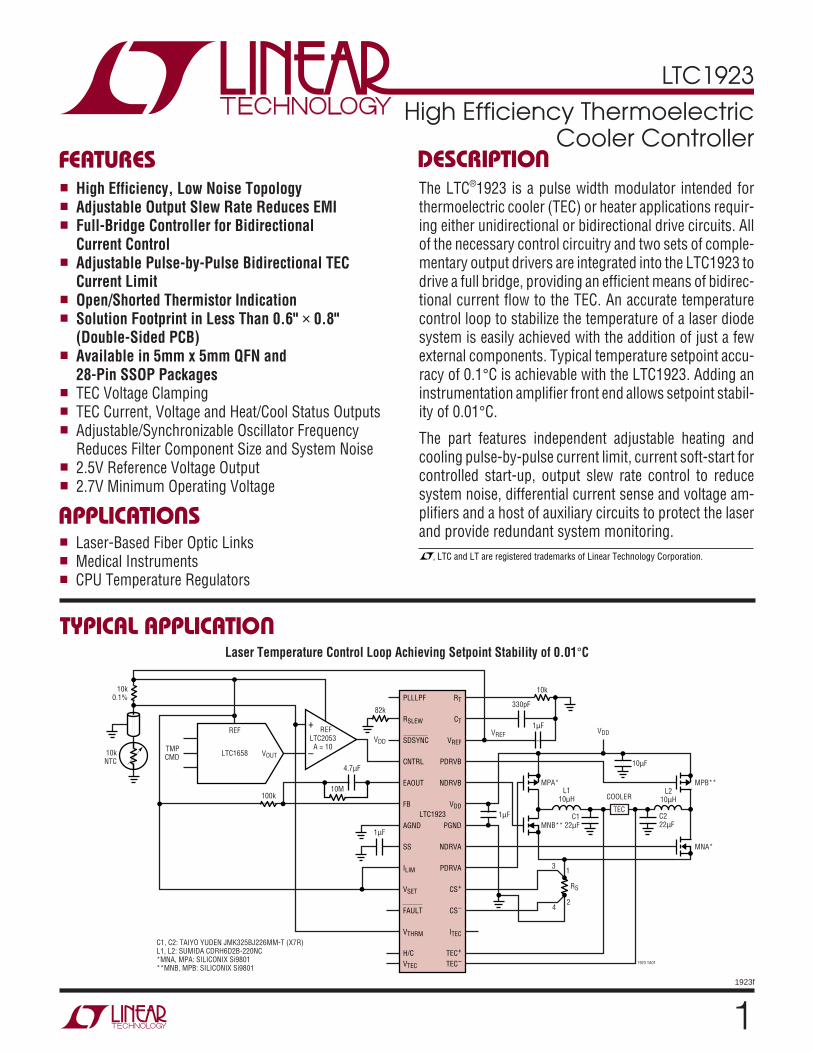
VDD to GND................................................. –0.3V to 6VSDSYNC, RSLEW ......................................... –0.3V to 6VFB, CNTRL, VTHRM, ILIM, VSET..................... –0.3V to 6VCS +, CS –, TEC+, TEC – .................................–0.3V to 6V
ORDER PARTNUMBER
LTC1923EGN
TJMAX = 125°C, θJA = 120°C/W
ABSOLUTE AXI U RATI GS
W WW U
PACKAGE/ORDER I FOR ATIOU UW
The denotes specifications which apply over the full operating temperature range, otherwise specifications are TA = 25°C.VDD = 5V, RSLEW = VDD, SDSYNC = VDD, RT = 10k, CT = 330pF unless otherwise noted.
ELECTRICAL CHARACTERISTICS
1
2
3
4
5
6
7
8
9
10
11
12
13
14
TOP VIEW
GN PACKAGE28-LEAD PLASTIC SSOP
28
27
26
25
24
23
22
21
20
19
18
17
16
15
PLLLPF
RSLEW
SDSYNC
CNTRL
EAOUT
FB
AGND
SS
ILIM
VSET
FAULT
VTHRM
H/C
VTEC
RT
CT
VREF
PDRVB
NDRVB
VDD
PGND
NDRVA
PDRVA
CS+
CS–
ITEC
TEC+
TEC–
Consult LTC Marketing for parts specified with wider operating temperature ranges.
(Note 1)
FAULT, H/C ................................................. –0.3V to 6VOperating Temperature Range (Note 2) .. –40°C to 85°CStorage Temperature Range ................. –65°C to 125°CLead Temperature (Soldering, 10 sec).................. 300°C
ORDER PARTNUMBER
LTC1923EUH32 31 30 29 28 27 26 25
9 10 11 12 13 14 15 16
17
18
19
20
21
22
23
24
8
7
6
5
4
3
2
1CNTRL
EAOUT
FB
AGND
NC
SS
ILIM
VSET
PDRVB
NDRVB
VDD
VDD
PGND
NDRVA
PDRVA
CS +
SDSY
NC
R SLE
W
PLLL
PF
R T C T V REF
NC NC
FAUL
T
V THR
M
H/C
V TEC
TEC
–
TEC
+
I TEC
CS–
UH PACKAGE32-LEAD PLASTIC QFN
PIN 1TOP VIEW
TJMAX = 125°C, θJA = 34°C/WEXPOSED PAD IS PGND
(MUST BE SOLDERED TO PCB)
SYMBOL PARAMETER CONDITIONS MIN TYP MAX UNITS
Input Supply
VDD Operating Supply Voltage 2.7 5.5 V
UVLO Undervoltage Lockout Low to High Threshold 2.6 2.7 V
UVHYST Hysteresis High to Low 50 130 mV
IDD Operating Supply Current No Output Load, Outputs Not Switching 2 4 mA
IDDSHDN Shutdown IDD SDSYNC = 0V 10 25 µA
SHDNTH Shutdown Threshold Measured at PDRVA, PDRVB 0.3 0.8 1.4 V
3
LTC1923
1923f
The denotes specifications which apply over the full operating temperature range, otherwise specifications are TA = 25°C.VDD = 5V, RSLEW = VDD, SDSYNC = VDD, RT = 10k, CT = 330pF unless otherwise noted.
ELECTRICAL CHARACTERISTICS
SYMBOL PARAMETER CONDITIONS MIN TYP MAX UNITS
Reference
VREF Reference Output Voltage No Load 2.462 2.5 2.538 V 2.450 2.550 V
VREFGD VREF Good Threshold VREF Rising Threshold 2.25 2.45 V
LDREG Load Regulation ILOAD = –1mA to –10mA 10 25 mV
LINEREG Line Regulation VDD = 2.7V to 5.5V 5 20 mV
VREFISC Short-Circuit Current VREF = 0V 10 20 mA
Oscillator and Phase-Locked Loop
fOSCI Initial Oscillator Frequency RT = 10k, CT = 330pF 190 225 260 kHz
fOSC Frequency Variation VDD = 2.7V to 5V, CT = 330pF, RT = 10k 165 225 270 kHz
OSCPK CT Ramp Peak 1.4 1.5 1.6 V
OSCVLY CT Ramp Valley 0.4 0.5 0.6 V
CTICH CT Charge Current CT = 0.3V, RT = 10k –150 µA
CTIDIS CT Discharge Current CT = 1.8V, RT = 10k 150 µAPLLGAIN Gain from PLLLPF to RT –1.1 –0.9 –0.7 V/VIPLLLPF Phase Detector Output Current
Sinking fSYNC < fOSC 12 µA Sourcing fSYNC > fOSC –12 µA
MSTTH Master Threshold On PLLLPF Pin Measured at SDSYNC Pin VDD – 0.7 VDD – 0.4 VSDDLY Shutdown Delay to Output 20 45 µsError AmplifierVOS Input Offset Voltage EAOUT = 1V, VCM = 2.5V –18 18 mVAOL Open-Loop Gain EAOUT = 0.45V to 1.55V, CNTRL = 2.5V 80 dBVCM Common Mode Input Range EAOUT = 1V 0.2 VDD + 0.2 VIIB FB and CNTRL Input Bias Currents FB = CNTRL = 1.25 –100 100 nAVOH Output High ILOAD = –100µA 1.65 VVOL Output Low ILOAD = 100µA 0.3 0.45 VISOURCE Sourcing Current EAOUT = 1V, FB = 2.4V, CNTRL = 2.5V –1.5 –0.5 mAISINK Sinking Current EAOUT = 1V, FB = 5V, CNTRL = 2.5V 1 2 mAGBW Gain-Bandwidth Product f = 100kHz (Note 3) 2 MHzCurrent Sense AmplifierACS Amplifier Gain 10 V/VCSOFF Amplifier Offset Measured at ITEC – 15 –2 10 mVITECH Output Sourcing Load Regulation CS + - CS– = 100mV, ILOAD = 0 to –50µA 0.1 0.2 VITECL Output Sinking Load Regulation CS + - CS– = 100mV, ILOAD = 0 to 50µA 0.1 0.2 Vf3dB –3dB Frequency (Note 3) 500 kHzILIMTH Current Limit Threshold Measured at CS+, CS– 125 145 165 mV
ILIMDLY Current Limit Delay to Output 300 450 nsSSICHG Soft-Start Charge Current SS = 0.75V –2.5 –1.5 –0.5 µASSILIM Soft-Start Current Limit Threshold SS = 0.5V, Measured at CS+, CS– 50 70 90 mVILIM ILIM Current Limit Threshold ILIM = 0.5V, Measured at CS+, CS– 50 70 90 mV
4
LTC1923
1923f
Note 1: Absolute Maximum Ratings are those values beyond which the lifeof a device may be impaired.Note 2: The LTC1923E is guaranteed to meet specifications from 0°C to70°C. Specifications over the –40°C to 85°C operating temperature rangeare assured by design, characterization and correlation with statisticalprocess controls.
ELECTRICAL CHARACTERISTICS
Note 3: Guaranteed by design, not tested in production.
The denotes specifications which apply over the full operating temperature range, otherwise specifications are TA = 25°C.VDD = 5V, RSLEW = VDD, SDSYNC = VDD, RT = 10k, CT = 330pF unless otherwise noted.
SYMBOL PARAMETER CONDITIONS MIN TYP MAX UNITSTEC Voltage AmplifierATEC Amplifier Gain 0.98 1 1.02 V/VTECOFF Amplifier Offset Measured at VTEC, VCM = 2.5V –7 mVTECCMR Common Mode Rejection 0.1V < VCM < 4.9V 60 dBVTECH Output High Voltage ILOAD = –50µA 4.7 4.9 VVTECL Output Low Voltage ILOAD = 50µA 0.1 0.3 Vf3dB –3dB Frequency (Note 3) 1 MHzOutput DriversOUTH Output High Voltage IOUT = –100mA 4 4.5 VOUTL Output Low Voltage IOUT = 100mA 0.7 1.2 VtRISE Output Rise Time CLOAD = 1nF 20 nstFALL Output Fall Time CLOAD = 1nF 20 nstrSLEW Output Rise Time CLOAD = 1nF, RSLEW = 10k 20 nstfSLEW Output Fall Time CLOAD = 1nF, RSLEW = 10k 20 nstrSLEW Output Rise Time CLOAD = 1nF, RSLEW = 100k 90 nstfSLEW Output Slew Fall Time CLOAD = 1nF, RSLEW = 100k 90 nsSLEWVT RSLEW Disable Threshold 2.75 VDLY Output Dead Time RT = 10k 90 nsFaultOPENTH Open Thermistor Threshold VSET = 5V, Measured with Respect to VSET –410 mVSHRTTH Shorted Thermistor Threshold VSET = 5V, Measured with Respect to GND 0.975 VFLTV Fault Output Low Voltage 1mA Into FAULT, During Fault 150 300 mVDirection ComparatorDIRH Low-to-High Threshold TEC – = 2.5V, Measured with Respect to TEC – 50 mV
Sensed When H/C Toggles LowDIRL High-to-Low Threshold TEC – = 2.5V, Measured with Respect to TEC – – 50 mV
Sensed When H/C Toggles HighHCV H/C Output Low Voltage 1mA Into Pin 150 300 mV
5
LTC1923
1923f
TEMPERATURE (°C)–50
165
OSCI
LLAT
OR F
REQU
ENCY
(kHz
)
185
205
225
265
–20 10 40 70
1923 G01
100 130
245
CT = 330pFRT = 10k
RT (kΩ)5
0
OSCI
LLAT
OR F
REQU
ENCY
(kHz
)
200
600
800
1000
15
1800
1923 G02
400
10 20
1200
1400
1600
CT = 68pF
CT = 150pF
CT = 330pF
VDD = 2.7V, 5VTA = 25°C
TEMPERATURE (°C)
V REF
(V)
2.495
2.500
1923 G03
2.490
2.485
2.510
2.505
–50 –20 10 40 70 100 130
TYPICAL PERFOR A CE CHARACTERISTICS
UW
VREF vs IREF for DifferentTemperatures Output Dead Time vs RT
Error Amplifier Offset Voltagevs Temperature
Open Thermistor Thresholdvs Temperature
Output Rise/Fall Time vs RSLEW
Shorted Thermistor Thresholdvs Temperature
IREF (mA)0
V REF
(V)
10
2.515
2.510
2.505
2.500
2.495
2.490
2.485
2.480
2.475
2.470
1923 G04
5 15
TA = 125°C
TA = 25°C
TA = –50°C
RT (kΩ)5
DEAD
TIM
E (n
s)
125
15
1923 G05
100
75
257.5 10 12.5
50
150
VDD = 2.7V
VDD = 5V
TA = 25°C
0
RISE
TIM
E (n
s)
100
150
1923 G06
50
0100 200 300
250
200
RSLEW (kΩ)
TA = 25°C
TEMPERATURE (°C)–50
–1.0
ERRO
R AM
PLIF
IER
V IO
(mV)
–0.5
0
0.5
1.0
1.5
–20 10 40 70
1923 G07
100 130TEMPERATURE (°C)
–504.55
OPEN
THE
RMIS
TOR
THRE
SHOL
D (V
)
4.56
4.57
4.58
4.59
4.60
–20 10 40 70
1923 G08
100 130
VSET = 5V
TEMPERATURE (°C)–50
0.95
SHOR
TED
THER
MIS
TOR
THRE
SHOL
D (V
)
0.96
0.97
0.98
0.99
1.00
–20 10 40 70
1923 G09
100 130
VSET = 5V
Oscillator Frequencyvs Temperature Oscillator Frequency vs RT VREF vs Temperature
6
LTC1923
1923f
TYPICAL PERFOR A CE CHARACTERISTICS
UW
Representative Waveforms for NDRVA,NDRVB, TEC Current and CS+ – CS–
Representative Waveforms forTEC Current, CS+ – CS– and ITEC
VDD = 5V 1923 G15.tif
RTEC = 2.5ΩRS = 0.1Ω
CH1: TEC CURRENT (500mA/DIV)
CH2: VOLTAGE ACROSS0.1Ω SENSE RESISTOR(CS + – CS –) 100mV/DIV
CH3: NDRVA (5V/DIV)
CH4: NDRVB (5V/DIV)
CH2: VOLTAGE ACROSS 0.1Ω SENSERESISTOR RS (CS + – CS –) 100mV/DIV
CH3: VOLTAGE ON ITEC PIN EQUAL TOTEN TIMES THE ABSOLUTE VALUE OFCH2 (200mV/DIV)
CH1: TEC CURRENT (500mA/DIV)
CH1, CH3
CH2
VDD = 5V 1923 G16.tif
RTEC = 2.5ΩRS = 0.1Ω
System Power Lossvs TEC Current
TEC Clamp Voltagevs Temperature
Current Limit Thresholdvs Temperature
TEMPERATURE (°C)–50
CURR
ENT
LIM
IT T
HRES
HOLD
(mV)
130
1923 G10
–20 4010 70 100
165
160
155
150
145
140
135
130
125
TEC CURRENT (A)0
0.4
0.5
0.7
1923 G11
0.3
0.2
0.5 1
0.1
0
0.6
POW
ER L
OSS
(W)
VDD = 5V
VDD = 3.3V
TA = 25°C
TEMPERATURE (°C)–50
TEC
CLAM
P VO
LTAG
E (V
)
130
1923 G12
–20 4010 70 100
2.550
2.530
2.510
2.490
2.470
2.450
7
LTC1923
1923f
Identical Test Conditions as Above, Except in Heating Mode. TEC’s Higher Heating Mode EfficiencyResults in Higher Thermal Gain. 0.002°C Peak-to-Peak Variation Is 4x Stability Improvement.Baseline Tilt, Just Detectable, Shows Similar 4x Improvement vs Above
Long-Term Cooling Mode Stability Measured in Environment that Steps 20 Degrees Above AmbientEvery Hour. Data Shows Resulting 0.008°C Peak-to-Peak Variation, Indicating Thermal Gain of2500. 0.0025°C Baseline Tilt Over Plot Length Derives From Varying Ambient Temperature
1923 G13.tif
1923 G14.tif
TYPICAL PERFOR A CE CHARACTERISTICS
UW
8
LTC1923
1923f
UUU
PI FU CTIO SPLLLPF (Pin 1/Pin 30): This pin serves as the lowpassfilter for the phase-locked loop when the part is beingsynchronized. The average voltage on this pin equallyalters both the oscillator charge and discharge currents,thereby changing the frequency of operation. Bringing thevoltage on this pin above VDD – 0.4V signifies that the partwill be used as the synchronization master. This allowsmultiple devices on the same board to be operated at thesame frequency. The SDSYNC pin will be pulled low duringeach CT charging cycle to facilitate synchronization.
RSLEW (Pin 2/Pin 31): Placing a resistor from this pin toAGND sets the voltage slew rate of the output driver pins.The minimum resistor value is 10k and the maximumvalue is 300k. Slew rate limiting can be disabled by tyingthis pin to VDD, allowing the outputs to transition at theirmaximum rate.
SDSYNC (Pin 3/Pin 32): This pin can be used to disable theIC, synchronize the internal oscillator or be the master tosynchronize other devices. Grounding this pin will disableall internal circuitry and cause NDRVA and NDRVB to beforced low and PDRVA and PDRVB to be forced to VDD.EAOUT will be forced low. FAULT will also be asserted lowindicating a fault condition. The pin can be pulled low forup to 20µs without triggering the shutdown circuitry. Thepart can either be slaved to an external clock or can be usedas the master (see Applications Information for a moredetailed explanantion).
CNTRL (Pin 4/Pin 1): Noninverting Input to the ErrorAmplifier.
EAOUT (Pin 5/Pin 2): Output of the Error Amplifier. Theloop compensation network is connected between this pinand FB. The voltage on this pin is the input to the PWMcomparator and commands anywhere between 0% and100% duty cycle to control the temperature of the tem-perature sense element.
FB (Pin 6/Pin 3): The Inverting Input to the Error Amplifier.This input is connected to EAOUT through a compensatingfeedback network.
AGND (Pin 7/Pin 4): Signal Ground. All voltages aremeasured with respect to AGND. Bypass VDD and VREFwith low ESR capacitors to the ground plane near this pin.
SS (Pin 8/Pin 6): The TEC current can be soft-started byadding a capacitor from this pin to ground. This capacitorwill be charged by a 1.5µA current source. This pin connectsto one of the inverting inputs of the current limit compara-tor and allows the TEC current to be linearly ramped up fromzero. The voltage on this pin must be greater than 1.5V toallow the open/shorted thermistor window comparitor tosignal a fault.
ILIM (Pin 9/Pin 7): A voltage divider from VREF to this pinsets the current limit threshold for the TEC. If the voltageon this pin is set higher than 1V, then ILIMIT = 150mV/RSas that is the internal current limit comparator level. If thevoltage on this pin is set less than 1V, the current limitvalue where the comparator trips is:
ILIMIT = [0.15 • RILIM1 • VREF]/[(RILIM1 + RILIM2) • RS]
VSET (Pin 10/Pin 8): This is the input for the setpointreference of the temperature sense element divider net-work or bridge. This pin must be connected to the biassource for the thermistor divider network.
FAULT (Pin 11/Pin 9): Open-drain output that indicates bypulling low when the voltage on VTHRM is outside thespecified window, the part is in shutdown, undervoltagelockout (UVLO), or the reference is not good. When thevoltage on VTHRM is outside the specified window, itsignifies that the thermistor impedance is out of its accept-able range. This signal can be used to flag a microcontrollerto shut the system down or used to disconnect power fromthe bridge. See Applications Information for using thissignal for redundant protection.
VTHRM (Pin 12/Pin 10): Voltage Across the Thermistor. Ifthe voltage on this pin is outside the range between 410mVbelow VSET and 0.2 • VSET, the FAULT pin will be asserted(and latched) low indicating that the thermistor tempera-ture has moved outside the acceptable range.
H/C (Pin 13/Pin 11): This open-drain output provides thedirection information of the TEC current flow. If TEC+ isgreater than TEC –, which typically corresponds to thesystem cooling, this output will be a logic low. If theopposite is the case, this pin will pull to a logic high.
(GN Package/UH Package)
9
LTC1923
1923f
UUU
PI FU CTIO SNDRVA, NDRVB (Pins 21, 24/Pins 19, 23): These push-pull outputs are configured to drive the opposite low sideswitches in a full-bridge arrangement.
PGND (Pin 22/Pin 20): This is the high current ground forthe IC. The external current sense resistor should bereferenced to this point.
VDD (Pin 23/Pins 21, 22): Positive Supply Rail for the IC.Bypass this pin to PGND and AGND with >10µF low ESL,ESR ceramic capacitors. The turn on voltage level for VDDis 2.6V with 130mV of hysteresis.
VREF (Pin 26/Pin 27): This is the output of the Reference.This pin should be bypassed to GND with a 1µF ceramiccapacitor. The reference is able to supply a minimum of10mA of current and is internally short-circuit currentlimited.
CT (Pin 27/Pin 28): The triangular wave oscillator timingcapacitor pin is used in conjunction with RT to set theoscillator frequency. The equation for calculating fre-quency is:
fR C
HzOSCT T
= 0 75.•
RT (Pin 28/Pin 29): A single resistor from RT to AGND setsthe charging and discharging currents for the triangleoscillator. This pin also sets the dead time between turningone set of outputs off and turning the other set on to ensurethe outputs do not cross conduct. The voltage on this pinis regulated to 0.5V. For best performance, the currentsourced from the RT pin should be limited to a maximum150µA. Selecting RT to be 10k is recommended andprovides 90ns of dead time.
VTEC (Pin 14/Pin 12): Output of the differential TEC voltageamplifier equal to the magnitude of the voltage acrossthe TEC.
TEC– (Pin 15/Pin 13): Inverting Input to the Differential TECVoltage Amplifier. This amplifier has a fixed gain of 1 with itsoutput being the voltage across the TEC with respect toAGND. This input, along with TEC+, signifies whether theTEC is heating or cooling the laser as indicated by theH/C pin.
TEC+ (Pin 16/Pin 14): Noninverting Input to the Differen-tial TEC Voltage Amplifier.
ITEC (Pin 17/Pin 15): Output of the Differential CurrentSense Amplifier. The voltage on this pin is equal to 10 •(ITEC + IRIPPLE) • RS, where ITEC is the thermoelectriccooler current, IRIPPLE is the inductor ripple current and RSis the sense resistor used to sense this current. Thisvoltage represents only the magnitude of the current andprovides no direction information. Current limit occurswhen the voltage on this pin exceeds the lesser of 1.5times the voltage on SS, 1.5 times the voltage on ILIM or1.5V. When this condition is present, the pair of outputs,which are presently conducting, are immediately turnedoff. The current limit condition is cleared when the CT pinreaches the next corresponding peak or valley (see Cur-rent Limit section).
CS – (Pin 18/Pin 16): Inverting Input to the DifferentialCurrent Sense Amplifier.
CS+ (Pin 19/Pin 17): Noninverting Input of the DifferentialCurrent Sense Amplifier. The amplifier has a fixed gainof 10.
PDRVA, PDRVB (Pins 20, 25/Pins 18, 24): These push-pull outputs are configured to drive the opposite high sidePMOS switches in a full-bridge arrangement.
(GN Package/UH Package)
10
LTC1923
1923f
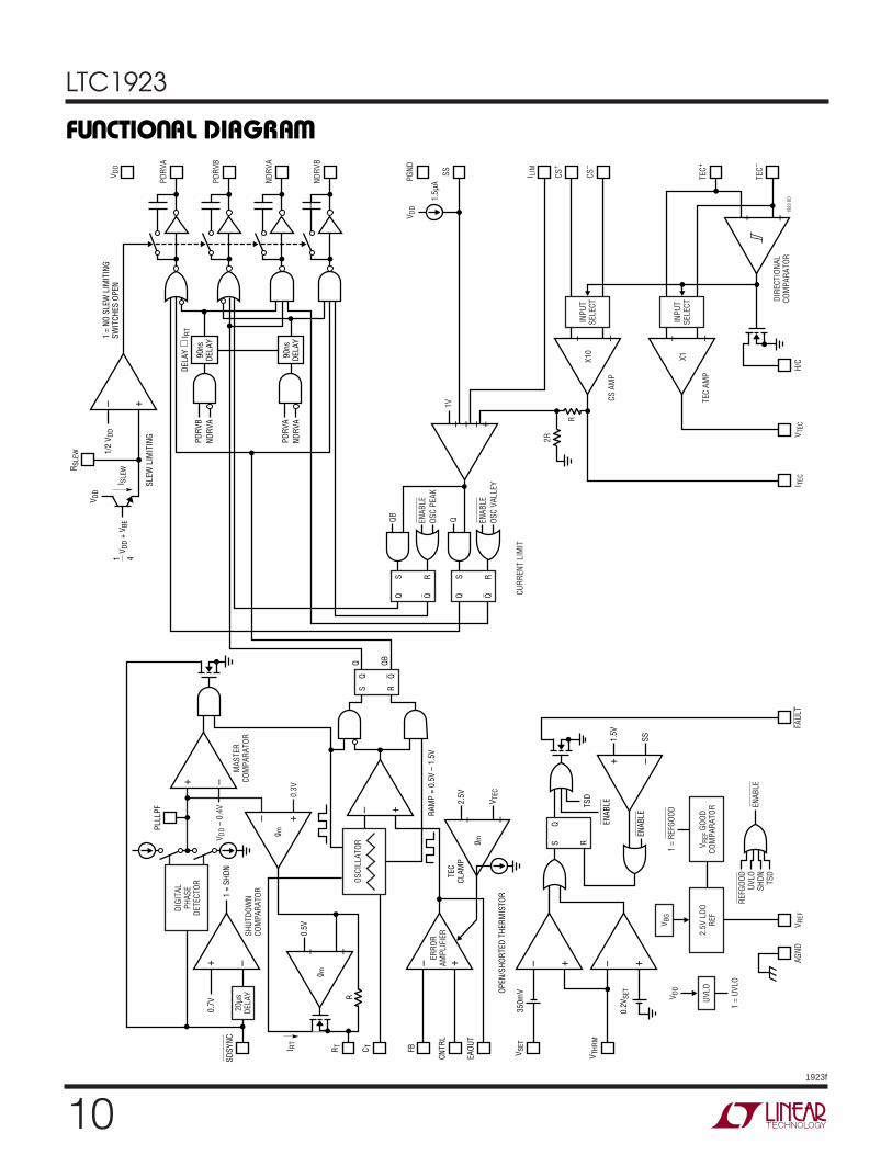
FU CTIO AL DIAGRA
UU W
– + – +
–+
– +
– +
– +
– – – +
TSD
1.5V
SS
ENAB
LE
ENAB
LE
S R
Q
SQ
1/2
V DD
1 =
NO S
LEW
LIM
ITIN
GSW
ITCH
ES O
PEN
QBR
Q Q
350m
VOPEN
/SHO
RTED
THE
RMIS
TOR
0.2V
SET
V SET
CNTR
L
–+
SDSY
NC
PLLL
PF
R SLE
W
SLEW
LIM
ITIN
G
V DD
I SLE
W
0.7V
1 =
SHDN
V DD
+ V B
E
EAOU
T
FBC T
RAM
P =
0.5V
– 1
.5V
R T
0.5V
I RT
R
V THR
M
DIGI
TAL
PHAS
EDE
TECT
OR
SHUT
DOW
NCO
MPA
RATO
R
MAS
TER
COM
PARA
TOR
OSCI
LLAT
OR
ERRO
RAM
PLIF
IER
FAUL
TI T
ECV T
ECH/
C19
23 B
D
TEC+
CS–
CS+
I LIMSS
1.5µ
APGND
NDRV
B
V DD
TEC–
2.5V
LDO
REF
V REF
AGND
REFG
OOD
UVLO
SHDN TS
D
V BG
V REF
GOO
DCO
MPA
RATO
R
1 =
REFG
OOD EN
ABLE
UVLO
1 =
UVLO
V DD
20µs
DELA
Y
R
2R
Q ENAB
LEOS
C VA
LLEY
CURR
ENT
LIM
IT
1V
–+
INPU
TSE
LECT
X10
CS A
MP
TEC
AMP
–+
–+
INPU
TSE
LECT
DIRE
CTIO
NAL
COM
PARA
TOR
X1
–+
– +
0.3V
V DD
– 0.
4V
–+
g m
2.5V
TEC
CLAM
P
V TEC
–+
g m
g m
Q Q
S R
QB ENAB
LEOS
C PE
AK
Q Q
S R
NDRV
A
PDRV
B
PDRV
A
V DD
90ns
DELA
YPD
RVA
PDRV
B
NDRV
A
90ns
DELA
Y
DELA
Y ∝
I RT
NDRV
A
1 4
11
LTC1923
1923f
OPERATIOU
MAIN CONTROL LOOP
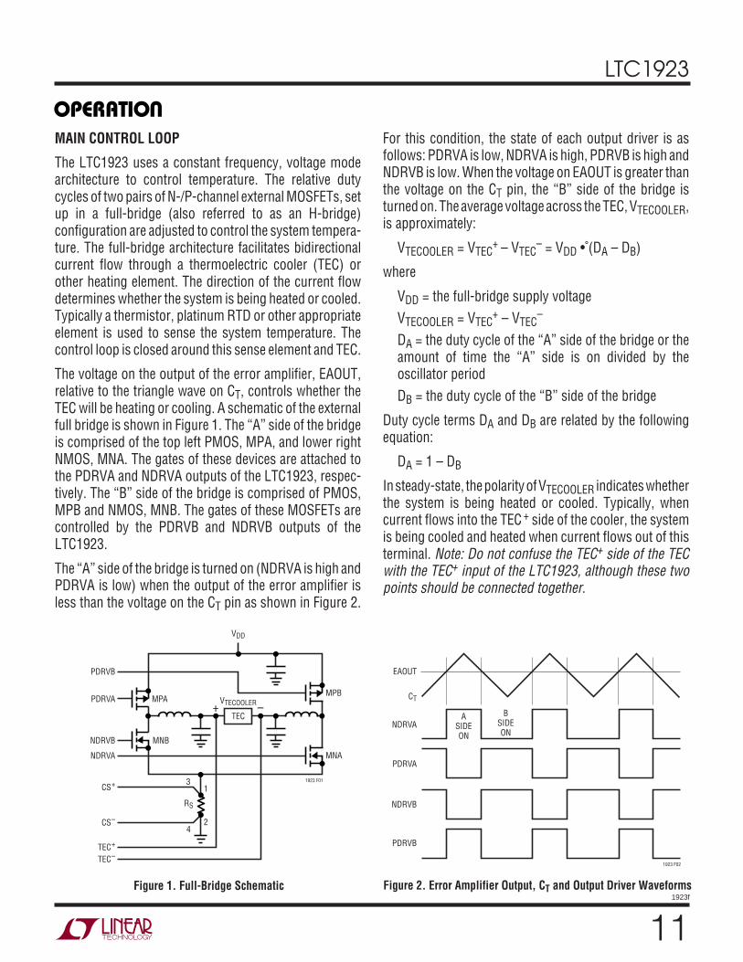
The LTC1923 uses a constant frequency, voltage modearchitecture to control temperature. The relative dutycycles of two pairs of N-/P-channel external MOSFETs, setup in a full-bridge (also referred to as an H-bridge)configuration are adjusted to control the system tempera-ture. The full-bridge architecture facilitates bidirectionalcurrent flow through a thermoelectric cooler (TEC) orother heating element. The direction of the current flowdetermines whether the system is being heated or cooled.Typically a thermistor, platinum RTD or other appropriateelement is used to sense the system temperature. Thecontrol loop is closed around this sense element and TEC.
The voltage on the output of the error amplifier, EAOUT,relative to the triangle wave on CT, controls whether theTEC will be heating or cooling. A schematic of the externalfull bridge is shown in Figure 1. The “A” side of the bridgeis comprised of the top left PMOS, MPA, and lower rightNMOS, MNA. The gates of these devices are attached tothe PDRVA and NDRVA outputs of the LTC1923, respec-tively. The “B” side of the bridge is comprised of PMOS,MPB and NMOS, MNB. The gates of these MOSFETs arecontrolled by the PDRVB and NDRVB outputs of theLTC1923.
The “A” side of the bridge is turned on (NDRVA is high andPDRVA is low) when the output of the error amplifier isless than the voltage on the CT pin as shown in Figure 2.
For this condition, the state of each output driver is asfollows: PDRVA is low, NDRVA is high, PDRVB is high andNDRVB is low. When the voltage on EAOUT is greater thanthe voltage on the CT pin, the “B” side of the bridge isturned on. The average voltage across the TEC, VTECOOLER,is approximately:
VTECOOLER = VTEC+ – VTEC
– = VDD • (DA – DB)
where
VDD = the full-bridge supply voltageVTECOOLER = VTEC
+ – VTEC–
DA = the duty cycle of the “A” side of the bridge or theamount of time the “A” side is on divided by theoscillator periodDB = the duty cycle of the “B” side of the bridge
Duty cycle terms DA and DB are related by the followingequation:
DA = 1 – DB
In steady-state, the polarity of VTECOOLER indicates whetherthe system is being heated or cooled. Typically, whencurrent flows into the TEC + side of the cooler, the systemis being cooled and heated when current flows out of thisterminal. Note: Do not confuse the TEC+ side of the TECwith the TEC+ input of the LTC1923, although these twopoints should be connected together.
4
3
2
1
MNA
1923 F01
MPBMPA
–+
MNBNDRVB
NDRVA
CS+
CS–
TEC+
TEC–
PDRVA
PDRVB
TEC
VTECOOLER
VDD
RS
NDRVAA
SIDEON
BSIDEON
EAOUT
CT
PDRVA
NDRVB
PDRVB
1923 F02
Figure 1. Full-Bridge Schematic Figure 2. Error Amplifier Output, CT and Output Driver Waveforms
12
LTC1923
1923f
PROTECTION FEATURES
Many protection features have been integrated into theLTC1923 to ensure that the TEC is not overstressed or thesystem does not thermally run away. These featuresinclude pulse-by-pulse current limiting, TEC voltage clamp-ing and open/shorted thermistor detection.
Current Limit
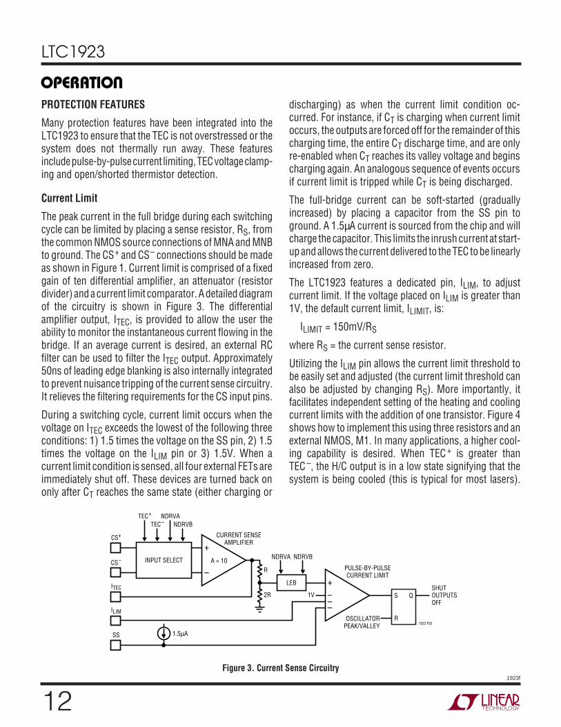
The peak current in the full bridge during each switchingcycle can be limited by placing a sense resistor, RS, fromthe common NMOS source connections of MNA and MNBto ground. The CS+ and CS– connections should be madeas shown in Figure 1. Current limit is comprised of a fixedgain of ten differential amplifier, an attenuator (resistordivider) and a current limit comparator. A detailed diagramof the circuitry is shown in Figure 3. The differentialamplifier output, ITEC, is provided to allow the user theability to monitor the instantaneous current flowing in thebridge. If an average current is desired, an external RCfilter can be used to filter the ITEC output. Approximately50ns of leading edge blanking is also internally integratedto prevent nuisance tripping of the current sense circuitry.It relieves the filtering requirements for the CS input pins.
During a switching cycle, current limit occurs when thevoltage on ITEC exceeds the lowest of the following threeconditions: 1) 1.5 times the voltage on the SS pin, 2) 1.5times the voltage on the ILIM pin or 3) 1.5V. When acurrent limit condition is sensed, all four external FETs areimmediately shut off. These devices are turned back ononly after CT reaches the same state (either charging or
OPERATIOU
discharging) as when the current limit condition oc-curred. For instance, if CT is charging when current limitoccurs, the outputs are forced off for the remainder of thischarging time, the entire CT discharge time, and are onlyre-enabled when CT reaches its valley voltage and beginscharging again. An analogous sequence of events occursif current limit is tripped while CT is being discharged.
The full-bridge current can be soft-started (graduallyincreased) by placing a capacitor from the SS pin toground. A 1.5µA current is sourced from the chip and willcharge the capacitor. This limits the inrush current at start-up and allows the current delivered to the TEC to be linearlyincreased from zero.
The LTC1923 features a dedicated pin, ILIM, to adjustcurrent limit. If the voltage placed on ILIM is greater than1V, the default current limit, ILIMIT, is:
ILIMIT = 150mV/RS
where RS = the current sense resistor.
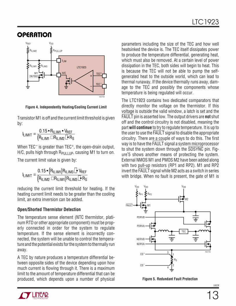
Utilizing the ILIM pin allows the current limit threshold tobe easily set and adjusted (the current limit threshold canalso be adjusted by changing RS). More importantly, itfacilitates independent setting of the heating and coolingcurrent limits with the addition of one transistor. Figure 4shows how to implement this using three resistors and anexternal NMOS, M1. In many applications, a higher cool-ing capability is desired. When TEC + is greater thanTEC –, the H/C output is in a low state signifying that thesystem is being cooled (this is typical for most lasers).
–
+A = 10
R
2R 1V
NDRVB
CURRENT SENSEAMPLIFIER
PULSE-BY-PULSECURRENT LIMIT
TEC–
CS+
CS–
NDRVATEC+
NDRVB
OSCILLATORPEAK/VALLEY
NDRVA
ITEC
ILIM
SS 1.5µA
INPUT SELECT
LEB
S
1923 F03
SHUT OUTPUTSOFF
R
Q
–––
+
Figure 3. Current Sense Circuitry
13
LTC1923
1923f
Transistor M1 is off and the current limit threshold is givenby:
IR V
R R RLIMITILIM REF
ILIM ILIM S=
+( )0 15 1
1 2
. • ••
When TEC– is greater than TEC+, the open-drain output,H/C, pulls high through RPULLUP, causing M1 to turn on.
The current limit value is given by:
IR R V
R R R RLIMITILIM ILIM REF
ILIM ILIM ILIM S=
( )+( )
0 15 1 3
2 1 3
. • •
•
reducing the current limit threshold for heating. If theheating current limit needs to be greater than the coolinglimit, an extra inversion can be added.
Open/Shorted Thermistor Detection
The temperature sense element (NTC thermistor, plati-num RTD or other appropriate component) must be prop-erly connected in order for the system to regulatetemperature. If the sense element is incorrectly con-nected, the system will be unable to control the tempera-ture and the potential exists for the system to thermally runaway.
A TEC by nature produces a temperature differential be-tween opposite sides of the device depending upon howmuch current is flowing through it. There is a maximumlimit to the amount of temperature differential that can beproduced, which depends upon a number of physical
OPERATIOU
parameters including the size of the TEC and how wellheatsinked the device is. The TEC itself dissipates powerto produce the temperature differential, generating heat,which must also be removed. At a certain level of powerdissipation in the TEC, both sides will begin to heat. Thisis because the TEC will not be able to pump the self-generated heat to the outside world, which can lead tothermal runaway. If the device thermally runs away, dam-age to the TEC and possibly the components whosetemperature is being regulated will occur.
The LTC1923 contains two dedicated comparators thatdirectly monitor the voltage on the thermistor. If thisvoltage is outside the valid window, a latch is set and theFAULT pin is asserted low. The output drivers are not shutoff and the control circuitry is not disabled, meaning thepart will continue to try to regulate temperature. It is up tothe user to use the FAULT signal to disable the appropriatecircuitry. There are a couple of ways to do this. The firstway is to have the FAULT signal a system microprocessorto shut the system down through the SDSYNC pin. Fig-ure 5 shows another means of protecting the system.External NMOS M1 and PMOS M2 have been added alongwith two pull-up resistors (RP1 and RP2). M1 and RP2invert the FAULT signal while M2 acts as a switch in serieswith bridge. When no fault is present, the gate of M1 is
–
+H/CM1
2N7002
LTC1923
ILIM
TEC+
TEC –
1923 F04
RLIM3RILIM1
RILIM2
VREF VDD
RPULLUP
Figure 4. Independently Heating/Cooling Current Limit
4
3
2
11923 F05
NDRVB
NDRVA
CS+
RS
CS–
PDRVA
PDRVB
FAULT M1
M2
RP2
TEC
VDD VDDVDD
RP1
Figure 5. Redundant Fault Protection
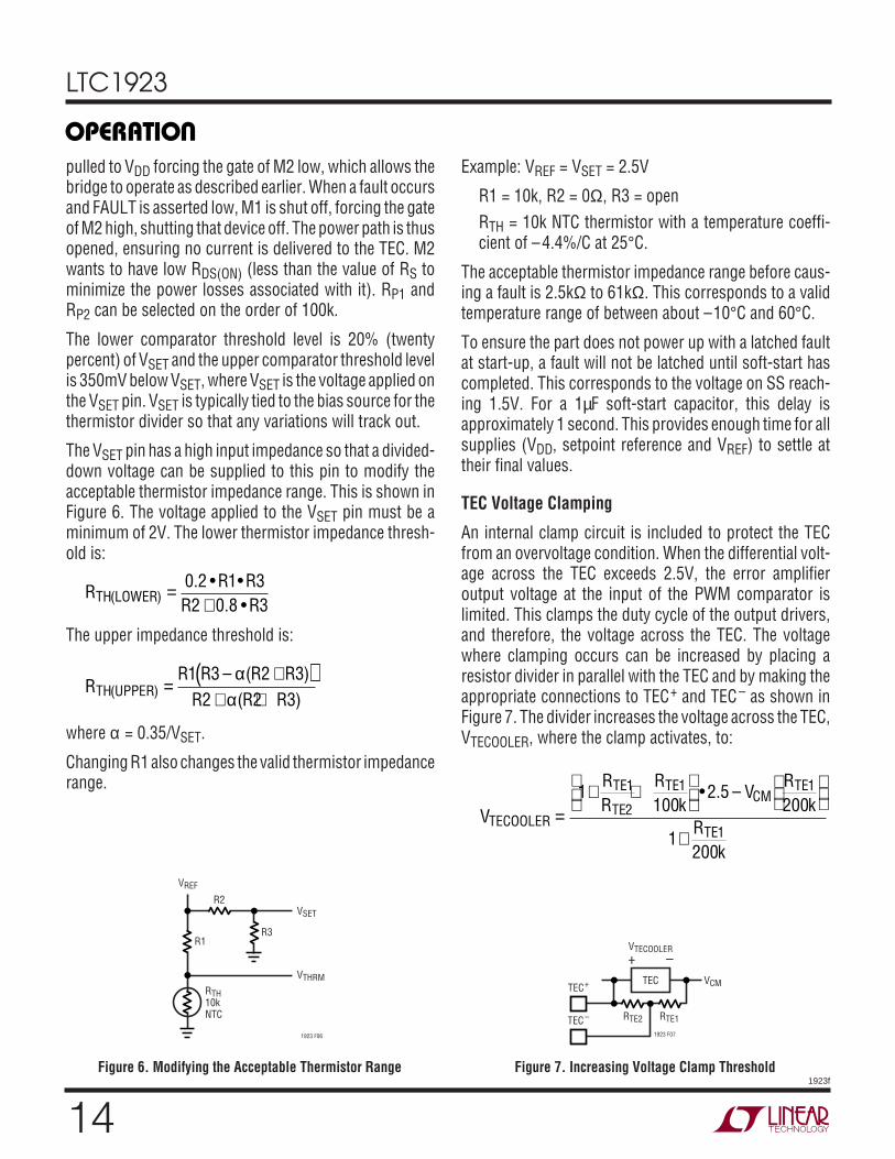
14
LTC1923
1923f
pulled to VDD forcing the gate of M2 low, which allows thebridge to operate as described earlier. When a fault occursand FAULT is asserted low, M1 is shut off, forcing the gateof M2 high, shutting that device off. The power path is thusopened, ensuring no current is delivered to the TEC. M2wants to have low RDS(ON) (less than the value of RS tominimize the power losses associated with it). RP1 andRP2 can be selected on the order of 100k.
The lower comparator threshold level is 20% (twentypercent) of VSET and the upper comparator threshold levelis 350mV below VSET, where VSET is the voltage applied onthe VSET pin. VSET is typically tied to the bias source for thethermistor divider so that any variations will track out.
The VSET pin has a high input impedance so that a divided-down voltage can be supplied to this pin to modify theacceptable thermistor impedance range. This is shown inFigure 6. The voltage applied to the VSET pin must be aminimum of 2V. The lower thermistor impedance thresh-old is:
RR R
R RTH LOWER( ). • •
. •=
+0 2 1 32 0 8 3
The upper impedance threshold is:
RR R R R
R R RTH UPPER( )– ( )
( )=
+( )+ +
1 3 2 32 2 3
αα
where α = 0.35/VSET.
Changing R1 also changes the valid thermistor impedancerange.
Example: VREF = VSET = 2.5V
R1 = 10k, R2 = 0Ω, R3 = openRTH = 10k NTC thermistor with a temperature coeffi-cient of –4.4%/C at 25°C.
The acceptable thermistor impedance range before caus-ing a fault is 2.5kΩ to 61kΩ. This corresponds to a validtemperature range of between about –10°C and 60°C.
To ensure the part does not power up with a latched faultat start-up, a fault will not be latched until soft-start hascompleted. This corresponds to the voltage on SS reach-ing 1.5V. For a 1µF soft-start capacitor, this delay isapproximately 1 second. This provides enough time for allsupplies (VDD, setpoint reference and VREF) to settle attheir final values.
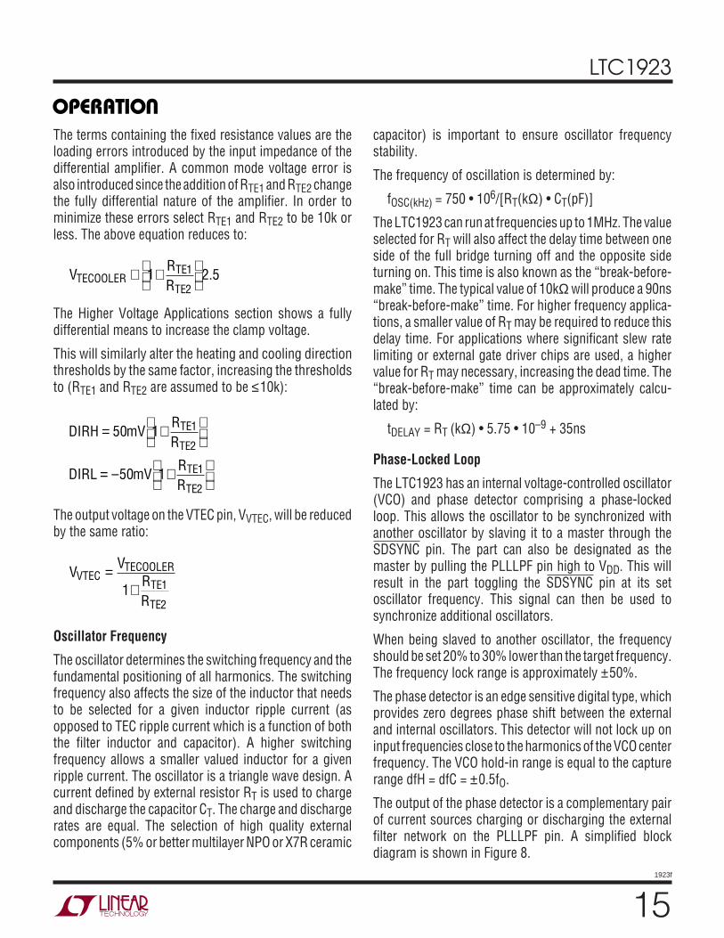
TEC Voltage Clamping
An internal clamp circuit is included to protect the TECfrom an overvoltage condition. When the differential volt-age across the TEC exceeds 2.5V, the error amplifieroutput voltage at the input of the PWM comparator islimited. This clamps the duty cycle of the output drivers,and therefore, the voltage across the TEC. The voltagewhere clamping occurs can be increased by placing aresistor divider in parallel with the TEC and by making theappropriate connections to TEC+ and TEC – as shown inFigure 7. The divider increases the voltage across the TEC,VTECOOLER, where the clamp activates, to:
V
RR
Rk
VR
kR
k
TECOOLER
TE
TE
TECM
TE
TE=
+ +
+
1100
2 5200
1200
1
2
1 1
1
• . –
VREF
VSET
VTHRM
1923 F06
R2
R1
RTH10kNTC
R3
Figure 6. Modifying the Acceptable Thermistor Range
TECTEC+
RTE2 RTE1
1923 F07
VTECOOLER
VCM
+ –
TEC –
Figure 7. Increasing Voltage Clamp Threshold
OPERATIOU
15
LTC1923
1923f
The terms containing the fixed resistance values are theloading errors introduced by the input impedance of thedifferential amplifier. A common mode voltage error isalso introduced since the addition of RTE1 and RTE2 changethe fully differential nature of the amplifier. In order tominimize these errors select RTE1 and RTE2 to be 10k orless. The above equation reduces to:
VRRTECOOLER
TE
TE≅ +
1 2 51
2.
The Higher Voltage Applications section shows a fullydifferential means to increase the clamp voltage.
This will similarly alter the heating and cooling directionthresholds by the same factor, increasing the thresholdsto (RTE1 and RTE2 are assumed to be ≤10k):
DIRH mVRR
DIRL mVRR
TE
TE
TE
TE
= +
= +
50 1
50 1
1
2
1
2–
The output voltage on the VTEC pin, VVTEC, will be reducedby the same ratio:
VV
RR
VTECTECOOLER
TE
TE
=+1 1
2
Oscillator Frequency
The oscillator determines the switching frequency and thefundamental positioning of all harmonics. The switchingfrequency also affects the size of the inductor that needsto be selected for a given inductor ripple current (asopposed to TEC ripple current which is a function of boththe filter inductor and capacitor). A higher switchingfrequency allows a smaller valued inductor for a givenripple current. The oscillator is a triangle wave design. Acurrent defined by external resistor RT is used to chargeand discharge the capacitor CT. The charge and dischargerates are equal. The selection of high quality externalcomponents (5% or better multilayer NPO or X7R ceramic
capacitor) is important to ensure oscillator frequencystability.
The frequency of oscillation is determined by:
fOSC(kHz) = 750 • 106/[RT(kΩ) • CT(pF)]
The LTC1923 can run at frequencies up to 1MHz. The valueselected for RT will also affect the delay time between oneside of the full bridge turning off and the opposite sideturning on. This time is also known as the “break-before-make” time. The typical value of 10kΩ will produce a 90ns“break-before-make” time. For higher frequency applica-tions, a smaller value of RT may be required to reduce thisdelay time. For applications where significant slew ratelimiting or external gate driver chips are used, a highervalue for RT may necessary, increasing the dead time. The“break-before-make” time can be approximately calcu-lated by:
tDELAY = RT (kΩ) • 5.75 • 10–9 + 35ns
Phase-Locked Loop
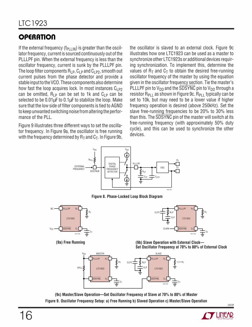
The LTC1923 has an internal voltage-controlled oscillator(VCO) and phase detector comprising a phase-lockedloop. This allows the oscillator to be synchronized withanother oscillator by slaving it to a master through theSDSYNC pin. The part can also be designated as themaster by pulling the PLLLPF pin high to VDD. This willresult in the part toggling the SDSYNC pin at its setoscillator frequency. This signal can then be used tosynchronize additional oscillators.
When being slaved to another oscillator, the frequencyshould be set 20% to 30% lower than the target frequency.The frequency lock range is approximately ±50%.
The phase detector is an edge sensitive digital type, whichprovides zero degrees phase shift between the externaland internal oscillators. This detector will not lock up oninput frequencies close to the harmonics of the VCO centerfrequency. The VCO hold-in range is equal to the capturerange dfH = dfC = ±0.5fO.
The output of the phase detector is a complementary pairof current sources charging or discharging the externalfilter network on the PLLLPF pin. A simplified blockdiagram is shown in Figure 8.
OPERATIOU
16
LTC1923
1923f
If the external frequency (fPLLIN) is greater than the oscil-lator frequency, current is sourced continuously out of thePLLLPF pin. When the external frequency is less than theoscillator frequency, current is sunk by the PLLLPF pin.The loop filter components RLP, CLP and CLP2, smooth outcurrent pulses from the phase detector and provide astable input to the VCO. These components also determinehow fast the loop acquires lock. In most instances CLP2can be omitted, RLP can be set to 1k and CLP can beselected to be 0.01µF to 0.1µF to stabilize the loop. Makesure that the low side of filter components is tied to AGNDto keep unwanted switching noise from altering the perfor-mance of the PLL.
Figure 9 illustrates three different ways to set the oscilla-tor frequency. In Figure 9a, the oscillator is free runningwith the frequency determined by RT and CT. In Figure 9b,
DIGITALPHASE
FREQUENCYDETECTOR
VDDVDD
PLLLPF
SDSYNCB
RT
RLP
CLP CLP2
OSC CT
RPLL
1923 F08
EXTERNALFREQUENCY
Figure 8. Phase-Locked Loop Block Diagram
the oscillator is slaved to an external clock. Figure 9cillustrates how one LTC1923 can be used as a master tosynchronize other LTC1923s or additional devices requir-ing synchronization. To implement this, determine thevalues of RT and CT to obtain the desired free-runningoscillator frequency of the master by using the equationgiven in the oscillator frequency section. Tie the master’sPLLLPF pin to VDD and the SDSYNC pin to VDD through aresistor RPLL as shown in Figure 9c. RPLL typically can beset to 10k, but may need to be a lower value if higherfrequency operation is desired (above 250kHz). Set theslave free-running frequencies to be 20% to 30% lessthan this. The SDSYNC pin of the master will switch at itsfree-running frequency (with approximately 50% dutycycle), and this can be used to synchronize the otherdevices.
OPERATIOU
PLLLPF
LTC1923
RT
SDSYNC
NC
VDD CT
RT
CT1923 F09a
PLLLPF
LTC1923
RT
SDSYNC
CLP2 RLP
CLP
CLKIN CT
RT
CT1923 F09b
PLLLPF
LTC1923
RT
SDSYNC
VDD
CT
RT
CT
PLLLPF
LTC1923
MASTER SLAVE
RT
1923 F09c
SDSYNC
CLP2 RLP
CLP
CT
1.2 • RT
CT
RPLL
(9a) Free Running (9b) Slave Operation with External Clock—Set Oscillator Frequency at 70% to 80% of External Clock
Figure 9. Oscillator Frequency Setup: a) Free Running b) Slaved Operation c) Master/Slave Operation(9c) Master/Slave Operation—Set Oscillator Frequency of Slave at 70% to 80% of Master
17
LTC1923
1923f
APPLICATIO S I FOR ATIO
WU UU
The thermistor may be isolated from the control circuitry.It has a relatively high input impedance and is thereforesusceptible to noise pick up. Extreme care should be takento ensure this signal is noise free by shielding the line(coaxially). A lowpass filter can be added between thethermistor and the input to the LTC2053, but since it is inthe signal path, there are limitations on how much filteringcan be added.
Inductor Ripple Current
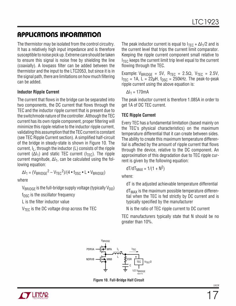
The current that flows in the bridge can be separated intotwo components, the DC current that flows through theTEC and the inductor ripple current that is present due tothe switchmode nature of the controller. Although the TECcurrent has its own ripple component, proper filtering willminimize this ripple relative to the inductor ripple current,validating this assumption that the TEC current is constant(see TEC Ripple Current section). A simplified half-circuitof the bridge in steady-state is shown in Figure 10. Thecurrent, IL, through the inductor (L) consists of the ripplecurrent (∆I1) and static TEC current (ITEC). The ripplecurrent magnitude, ∆I1, can be calculated using the fol-lowing equation:
∆I1 = (VBRIDGE2 – VTEC
2)/(4 • fOSC • L • VBRIDGE)
where
VBRIDGE is the full-bridge supply voltage (typically VDD)fOSC is the oscillator frequencyL is the filter inductor valueVTEC is the DC voltage drop across the TEC
The peak inductor current is equal to ITEC + ∆I1/2 and isthe current level that trips the current limit comparator.Keeping the ripple current component small relative toITEC keeps the current limit trip level equal to the currentflowing through the TEC.
Example: VBRIDGE = 5V, RTEC = 2.5Ω, VTEC = 2.5V,ITEC = 1A, L = 22µH, fOSC = 250kHz. The peak-to-peakripple current using the above equation is:
∆I1 = 170mA
The peak inductor current is therefore 1.085A in order toget 1A of DC TEC current.
TEC Ripple Current
Every TEC has a fundamental limitation (based mainly onthe TEC’s physical characteristics) on the maximumtemperature differential that it can create between sides.The ability to create this maximum temperature differen-tial is affected by the amount of ripple current that flowsthrough the device, relative to the DC component. Anapproximation of this degradation due to TEC ripple cur-rent is given by the following equation:
dT/dTMAX = 1/(1 + N2)
where:
dT is the adjusted achievable temperature differentialdTMAX is the maximum possible temperature differen-tial when the TEC is fed strictly by DC current and istypically specified by the manufacturerN is the ratio of TEC ripple current to DC current
TEC manufacturers typically state that N should be nogreater than 10%.
MPA
MNB
PDRVA
NDRVB ESRVTEC/2
C
1923 F10
+L
IL ITEC
TEC
1/2 VBRIDGE
VBRIDGE
Figure 10. Full-Bridge Half Circuit
18
LTC1923
1923f
APPLICATIO S I FOR ATIO
WU UU
In this application, the bridge supply voltage, oscillatorfrequency and external filter components determine theamount of ripple current that flows through the TEC.Higher valued filter components reduce the amount ofripple current through the TEC at the expense of increasedboard area. Filter capacitor ESR along with inductor ripplecurrent will determine the peak-to-peak voltage rippleacross the TEC and therefore the ripple current since theTEC appears resistive.
The ripple current through the TEC, ITEC(RIPPLE), isapproximately equal to:
IV V
f L C R V
V V ESR
f L V R
TEC RIPPLEBRIDGE TEC
OSC TEC BRIDGE
BRIDGE TEC
OSC BRIDGE TEC
( )–
• • • • •
– •
• • • •
≅
+( )
2 2
2
2 2
16
2
where:
fOSC = the oscillator frequencyL = the filter inductor valueC = the filter capacitor valueRTEC = the resistance of the TECVTEC = the DC voltage drop across the TECESR = the equivalent series resistance of the filtercapacitorVBRIDGE = the full-bridge supply voltage typically equalto VDD
The equation above shows that there are two components,which comprise TEC ripple current. The first term is theincrease in voltage from the charging of the filter capaci-tor. The second term is due to the filter capacitor ESR andis typically the dominant contributor. Therefore the filtercapacitor selected wants to have a low ESR. This capacitorcan be made of multilevel ceramic, OS-CON electrolytic orother suitable capacitor. Increasing the oscillator fre-quency will also reduce the TEC ripple current since bothterms have an inverse relationship to operating frequency.
Example: VBRIDGE = 5V, RTEC = 2.5Ω, VTEC = 2.5V,L = 22µH, C = 22µF, fOSC = 250kHz, ESR = 100mΩ
ITEC(RIPPLE) = 3.1mA + 13.6mA = 16.7mA
For this example the DC current flowing through the TECis 1A, making the ripple current equal to approximately 1.7%(this illustrates why ITEC can be approximated to be DC).
Closing the Feedback Loop
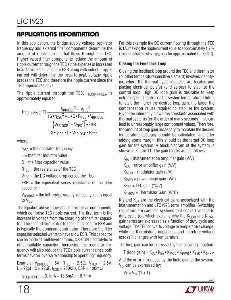
Closing the feedback loop around the TEC and thermistor(or other temperature sensitive element) involves identify-ing where the thermal system’s poles are located andplacing electrical pole(s) (and zeroes) to stabilize thecontrol loop. High DC loop gain is desirable to keepextremely tight control on the system temperature. Unfor-tunately the higher the desired loop gain, the larger thecompensation values required to stabilize the system.Given the inherently slow time constants associated withthermal systems (on the order of many seconds), this canlead to unreasonably large component values. Therefore,the amount of loop gain necessary to maintain the desiredtemperature accuracy should be calculated, and afteradding some margin, this should be the target DC loopgain for the system. A block diagram of the system isshown in Figure 11. The gain blocks are as follows:
KIA = instrumentation amplifier gain (V/V)KEA = error amplifier gain (V/V)KMOD = modulator gain (d/V)KPWR = power stage gain (V/d)KTEC = TEC gain (°C/V)KTHRM = Thermistor Gain (V/°C)
KIA and KEA are the electrical gains associated with theinstrumentation and LTC1923 error amplifier. Switchingregulators are sampled systems that convert voltage toduty cycle (d), which explains why the KMOD and KPWRgain terms are expressed as a function of duty cycle andvoltage. The TEC converts voltage to temperature change,while the thermistor’s impedance and therefore voltageacross it changes with temperature.
The loop gain can be expressed by the following equation:
T (loop gain) = KIA • KEA • KMOD • KPWR • KTEC • KTHRM
And the error introduced by the finite gain of the system,VE, can be expressed by:
VE = VIN/(1 + T)
19
LTC1923
1923f
APPLICATIO S I FOR ATIO
WU UU
VIN
+
–VE
CT
RA
RF
LTC1923LTC2053
CF
VREF
KTHRM KIA KEA KMOD KPWR KTEC
R110k
10kNTC –
+
–
+–
+POWERSTAGE
TEC
1923 F11
VTECOOLER
+
ERRORAMP
Figure 11. Simplified Loop Block Diagram
This voltage error translates back into a temperaturesetpoint error.
Example:
RTHRM = 10kNTC with 4.4%/°C at 25°CR1 = 10kVREF = 2.5VT = 25°C
For this thermistor with a 25°C temperature setpoint, thechange in thermistor voltage with temperature is given by–25mV/°C. In order to maintain a 0.01°C temperatureaccuracy, this translates into a 250µV error signal, VE. Theminimum loop gain can now be calculated from the aboveequation:
VE = VIN/(1 + T)
A 25°C setpoint temperature requires VIN = 1.25V forVREF = 2.5V. The required loop gain is 5000 or 74dB.
There are two handles to adjust the loop gain, KIA and KEA,while the other handles are fixed and depend upon the TECand thermistor characteristics (KTEC and KTHRM), VSET andR1 (KTHRM) and VDD (KMOD and KPWR). The modulator andpower gain product is given by:
KMOD • KPWR = 2 • VDD/VCT = 2 • VDD
where VCT = the CT voltage which has a fixed 1V amplitude.
The TEC gain depends upon the TEC selected and corre-sponds to the relationship between the voltage across thedevice and what temperature differential is created. Thisgain term changes with operating temperature, and whetherthe TEC is heating or cooling. TECs are inherently moreefficient at heating (and therefore have a higher gain) ascompared to cooling. A worst-case rough estimation ofthe gain can be obtained by taking the maximum TECvoltage required to force a given change in temperaturefrom the TEC specifications:
KTEC = dT/VTEC(MAX)
The thermistor gain should be linearized around tempera-ture setpoint.
Example:
Setpoint T = 25°CVDD = 5VRTHRM = 10k NTC with 4.4%/°C at 25°CR1 = 10kVREF = 2.5VdT/VTEC(MAX) = 45°C/1.5V = 30°C/V
20
LTC1923
1923f
TMPCMD
–
+–
+
REF
VOUT
LTC1658
10k
10kNTC
REFRC RA
RB
FB
CNTRL
EAOUT
LTC1923
ERRORAMPLIFIER
CA
6
5
1923 F124
A = 10
LTC2053
CB
CC
Figure 12. Alternative Compensation Method to Improve Transient Response
APPLICATIO S I FOR ATIO
WU UU
The linearized thermistor gain around 25°C is – 25mV/°C.For a minimum loop gain of 5000 as calculated above, thecombined gain of the instrumentation and error amplifierscan be calculated:
KIA • KEA = T/(KMOD • KPWR • KTEC • KTHRM)KIA • KEA = 5000/(10 • 30 • 0.025) = 667
A combined gain of 1000 can be selected to provideadequate margin. The instrumentation amplifier gain shouldbe set at typically 10, as this attenuates any errors by itsgain factor. The error amplifier gain would then be limitedto the remainder through the gain setting resistors, RF andRA shown in Figure 11.
RF/RA = KEA – 1
The multiple poles associated with the TEC/thermistorsystem makes it difficult to compensate. Compoundingthis problem is that there will be significant variations inthermal time constants for the same system, makingelaborate compensation schemes difficult to reliably imple-ment. The most robust method (i.e., least prone tooscillation) is to place a dominant pole well below thethermal system time constant (τ) (anywhere from manyseconds to minutes). This time constant will set thecapacitor value by the following equation:
CF = τ/RF
Please refer to Application Note 89 for more detailedinformation on compensating the loop. Ceramic capaci-tors are not recommended for use as the integratingcapacitor or anywhere in the signal path as they exhibit apiezoelectric effect which can introduce noise into the
system. The component values shown on the front page ofthis data sheet provide a good starting point, but someadjustment may be required to optimize the response.
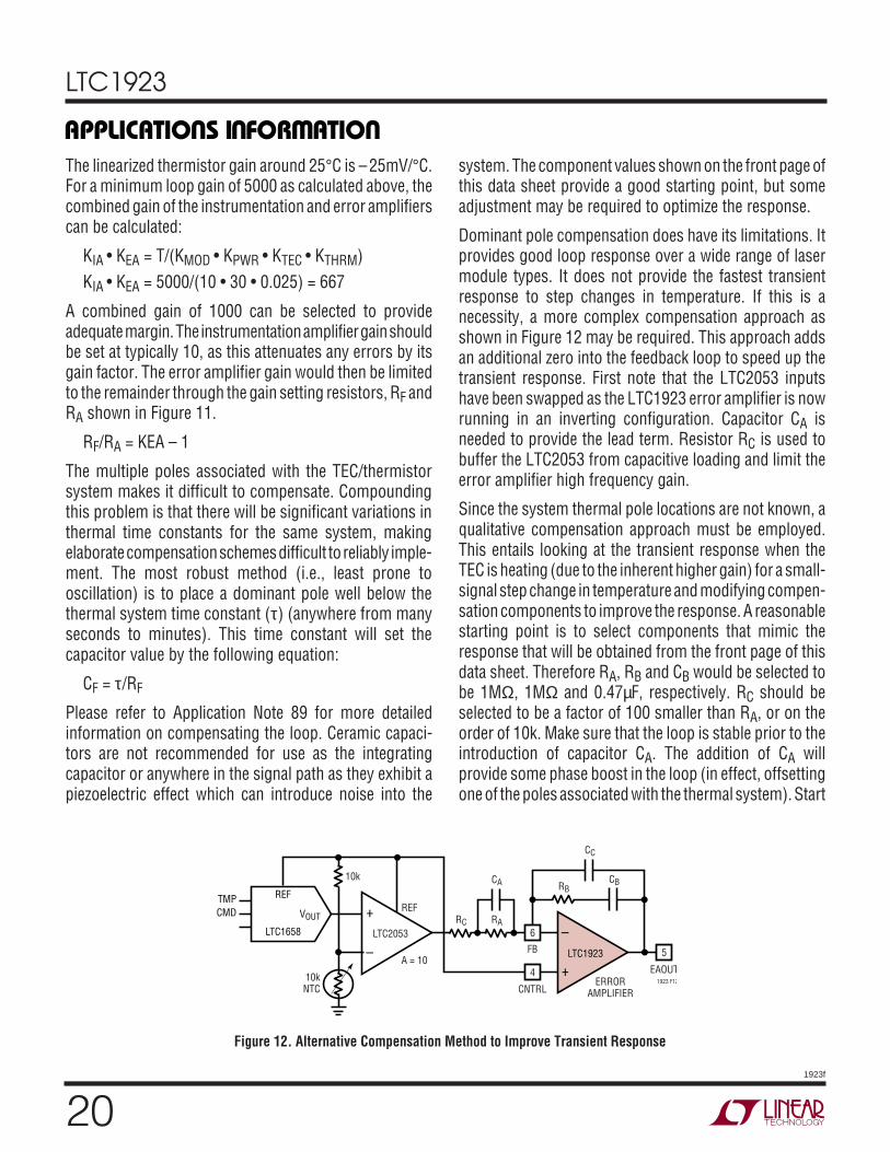
Dominant pole compensation does have its limitations. Itprovides good loop response over a wide range of lasermodule types. It does not provide the fastest transientresponse to step changes in temperature. If this is anecessity, a more complex compensation approach asshown in Figure 12 may be required. This approach addsan additional zero into the feedback loop to speed up thetransient response. First note that the LTC2053 inputshave been swapped as the LTC1923 error amplifier is nowrunning in an inverting configuration. Capacitor CA isneeded to provide the lead term. Resistor RC is used tobuffer the LTC2053 from capacitive loading and limit theerror amplifier high frequency gain.
Since the system thermal pole locations are not known, aqualitative compensation approach must be employed.This entails looking at the transient response when theTEC is heating (due to the inherent higher gain) for a small-signal step change in temperature and modifying compen-sation components to improve the response. A reasonablestarting point is to select components that mimic theresponse that will be obtained from the front page of thisdata sheet. Therefore RA, RB and CB would be selected tobe 1MΩ, 1MΩ and 0.47µF, respectively. RC should beselected to be a factor of 100 smaller than RA, or on theorder of 10k. Make sure that the loop is stable prior to theintroduction of capacitor CA. The addition of CA willprovide some phase boost in the loop (in effect, offsettingone of the poles associated with the thermal system). Start
21
LTC1923
1923f
APPLICATIO S I FOR ATIO
WU UU
–
+REF
VOUT
TMPCMD
LTC165810kNTC
LTC1923FB
ERRORAMPLIFIER
1923 F13
4.7µF10M
10k
100k6
CNTRL
4
EAOUT
5
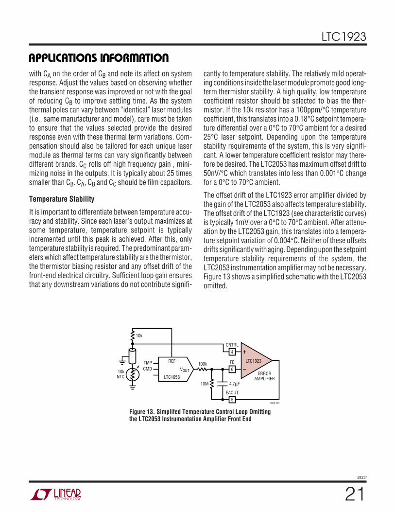
Figure 13. Simplifed Temperature Control Loop Omittingthe LTC2053 Instrumentation Amplifier Front End
with CA on the order of CB and note its affect on systemresponse. Adjust the values based on observing whetherthe transient response was improved or not with the goalof reducing CB to improve settling time. As the systemthermal poles can vary between “identical” laser modules(i.e., same manufacturer and model), care must be takento ensure that the values selected provide the desiredresponse even with these thermal term variations. Com-pensation should also be tailored for each unique lasermodule as thermal terms can vary significantly betweendifferent brands. CC rolls off high frequency gain , mini-mizing noise in the outputs. It is typically about 25 timessmaller than CB. CA, CB and CC should be film capacitors.
Temperature Stability
It is important to differentiate between temperature accu-racy and stability. Since each laser’s output maximizes atsome temperature, temperature setpoint is typicallyincremented until this peak is achieved. After this, onlytemperature stability is required. The predominant param-eters which affect temperature stability are the thermistor,the thermistor biasing resistor and any offset drift of thefront-end electrical circuitry. Sufficient loop gain ensuresthat any downstream variations do not contribute signifi-
cantly to temperature stability. The relatively mild operat-ing conditions inside the laser module promote good long-term thermistor stability. A high quality, low temperaturecoefficient resistor should be selected to bias the ther-mistor. If the 10k resistor has a 100ppm/°C temperaturecoefficient, this translates into a 0.18°C setpoint tempera-ture differential over a 0°C to 70°C ambient for a desired25°C laser setpoint. Depending upon the temperaturestability requirements of the system, this is very signifi-cant. A lower temperature coefficient resistor may there-fore be desired. The LTC2053 has maximum offset drift to50nV/°C which translates into less than 0.001°C changefor a 0°C to 70°C ambient.
The offset drift of the LTC1923 error amplifier divided bythe gain of the LTC2053 also affects temperature stability.The offset drift of the LTC1923 (see characteristic curves)is typically 1mV over a 0°C to 70°C ambient. After attenu-ation by the LTC2053 gain, this translates into a tempera-ture setpoint variation of 0.004°C. Neither of these offsetsdrifts significantly with aging. Depending upon the setpointtemperature stability requirements of the system, theLTC2053 instrumentation amplifier may not be necessary.Figure 13 shows a simplified schematic with the LTC2053omitted.
22
LTC1923
1923f
APPLICATIO S I FOR ATIO
WU UU
Noise and Slew Rate Control
One disadvantage of switching regulators is that theswitching creates wideband harmonic energy. The highfrequency content can pose problems to associated cir-cuitry. To combat this issue, the LTC1923 offers a pincalled RSLEW that controls the slew rate of the output drivewaveforms. Slowing down the transition interval reducesthe harmonic frequency content by spreading out theenergy over a longer time period. The additional transitiontime causes some efficiency loss (on the order of 2% to3%) but significantly improves the high frequency noisereflected onto the input supply.
Slew rate control is engaged by placing a resistor fromRSLEW to AGND. If slew rate control is not desired, the RSLEWpin should be tied to VDD allowing the output drivers totransition at their fastest rate. The resistor value should beset between 10k (fastest transition) and 300k (slowest tran-sition). This provides about a 10:1 slew rate range to op-timize noise performance. The “break-before-make” timemay need to be increased if slew control is implemented,especially for slower transition rates. Adjustment can bedone by increasing the value of RT (CT can be reduced tomaintain the same frequency of operation), to ensure thatthe bridge MOSFETs receive nonoverlapping drive.
Power MOSFET Selection
Four external MOSFETs must be selected for use with theLTC1923; a pair of N-channel MOSFETs for the bottom ofthe bridge and a pair of P-channel MOSFETs for the topdiagonals of the bridge. The MOSFETs should be selectedfor their RDS(ON), gate charge and maximum VDS, VGSratings. A maximum VDS rating of 20V is more thansufficient for 5V and 12V bridge applications, but asmentioned in the High Voltage Application section, a 12Vmaximum VGS rating is insufficient and higher voltageMOSFETs must be selected. There is a trade-off betweenRDS(ON) and gate charge. The RDS(ON) affects the conduc-tion losses (ITEC
2 • RDS(ON)), while gate charge is adominant contributor to switching losses. A higher RDS(ON)MOSFET typically has a smaller gate capacitance and thusrequires less current to charge the gate for the sameBVDSS. For 1A TEC applications, the Si9801DY or Si9928DYcomplimentary N- and P-channel MOSFETs provide a
good trade-off between switching and conduction losses.Above this TEC current level the MOSFETs selected shouldhave lower RDS(ON) to maintain the high end efficiency.
Efficiency Considerations
Unlike typical voltage regulators, where the output voltageis fixed, independent of load current, the output voltage ofthis regulator changes with load current. This is becausethe TEC appears resistive and the current through the TECsets the voltage. The output power of the regulator isdefined as:
POUT = ITEC2 • RTEC
The efficiency of a switching regulator is equal to theoutput power divided by the input power times 100%.Often it is useful to analyze individual losses to determinewhat is limiting the efficiency and which change wouldproduce the most significant improvement. Efficiency canbe expressed as:
Efficiency = 100% – (L1 + L2 + L3 + …)
where L1, L2, etc. are the individual losses as a percentageof input power.
For this application, the main efficiency concern is typi-cally at the high end of output power. A higher power losstranslates into a greater system temperature rise, result-ing in the need for heat sinking, increasing both the systemsize and cost.
There are three main sources which usually account formost of the losses in the application shown on the frontpage of the data sheet: Input supply current, MOSFETswitching losses and I2R losses.
1) The input supply current is comprised of the quiescentcurrent draw from the LTC1658, LTC2053, LTC1923 andany additional circuitry added. The total maximum supplycurrent for these devices is on the order of 5mA, whichgives a total power dissipation of 25mW. This power lossis independent of TEC current.
2) The MOSFET driver current results from switching thegate capacitance of the power MOSFETs. Each time a gateis switched from low to high to low again, a packet ofcharge dQ moves from VDD to ground. The gate chargingcurrent, IGATECHG = 2 • f • (QP + QN), where QP and QN are
23
LTC1923
1923f
APPLICATIO S I FOR ATIO
WU UU
the total gate charges of the NMOS and PMOS on one sideof the bridge, and f is the oscillator frequency. The factorof 2 arises from there being two sets of MOSFETs thatmake up the full bridge. Note that increasing the switchingfrequency will increase the dynamic current and thereforepower dissipation by the same factor. This power loss isindependent of TEC current.
Example: QN = 10nC max, QP = 15nC max, f = 225kHz,VDD = 5V
Power loss = 2 • f • (QP + QN) • VDD = 56mW
3) The DC resistances of the external bridge MOSFETs,filter inductors and sense resistor are typically the domi-nant loss mechanism at the high end TEC current. Theconduction path of the current includes one NMOS, onePMOS, two inductors and the sense resistor so the DCresistances associated with the components dissipatepower.
Example:
RDS(ON)NMOS at 5V = 0.055Ω max
RDS(ON)PMOS at 5V = 0.08Ω max
RS = 0.1Ω
RL = 0.1Ω,
ITEC = 1A
RTEC = 2.5Ω
Total series resistance = 0.055 + 0.08 + 2 • 0.1 + 0.1= 0.435Ω
Power Loss = (1A)2 • 0.435Ω = 0.435W
Output Power = (1A)2 • 2.5Ω = 2.5W
This represents a 17% efficiency loss due to conductionlosses. The other two power loss mechanisms comprisea little more than a 3% efficiency loss at this output powerlevel. This may sound alarming if electrical efficiency is theprimary concern and can be easily improved by choosinglower RDS(ON) MOSFETs, lower series resistance induc-tors and a smaller valued sense resistor. If temperaturerise is the primary concern, this power dissipation may beacceptable. At higher current levels, this example doesillustrate that lower resistance components should beselected.
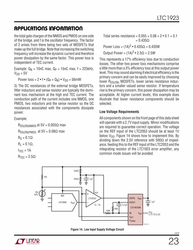
Low Voltage Requirements
All components shown on the front page of this data sheetwill operate with a 2.7V input supply. Minor modificationsare required to guarantee correct operation. The voltageon the REF input of the LTC2053 should be at least 1Vbelow VDD. Figure 14 shows how to implement this. Bydividing down the 2.5V reference with 500Ω of imped-ance, feeding this to the REF input of the LTC2053 and theintegrating resistor of the LTC1923 error amplifier, anycommon mode issues will be avoided.
REF
VOUTLTC1658
10kNTC
A = 10
100k
1923 F14
4.7µF
10M
REF
10k
1µF
VDD2.7V TO 3.3V
CNTRL VREF
VDD
EAOUT
FB
VSET
VTHRM
250Ω
250Ω
1µF
–
+LTC2053
LTC1923GN
Figure 14. Low Input Supply Voltage Circuit
24
LTC1923
1923f
APPLICATIO S I FOR ATIO
WU UU
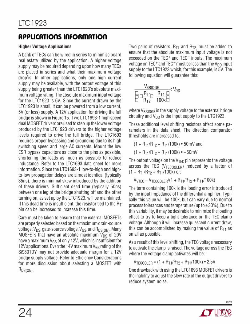
Higher Voltage Applications
A bank of TECs can be wired in series to minimize boardreal estate utilized by the application. A higher voltagesupply may be required depending upon how many TECsare placed in series and what their maximum voltagedrop is. In other applications, only one high currentsupply may be available, with the output voltage of thissupply being greater than the LTC1923’s absolute maxi-mum voltage rating. The absolute maximum input voltagefor the LTC1923 is 6V. Since the current drawn by theLTC1923 is small, it can be powered from a low current,5V (or less) supply. A 12V application for driving the fullbridge is shown in Figure 15. Two LTC1693-1 high speeddual MOSFET drivers are used to step up the lower voltageproduced by the LTC1923 drivers to the higher voltagelevels required to drive the full bridge. The LTC1693requires proper bypassing and grounding due to its highswitching speed and large AC currents. Mount the lowESR bypass capacitors as close to the pins as possible,shortening the leads as much as possible to reduceinductance. Refer to the LTC1693 data sheet for moreinformation. Since the LTC1693-1 low-to-high and high-to-low propagation delays are almost identical (typically35ns), there is minimal skew introduced by the additionof these drivers. Sufficient dead time (typically 50ns)between one leg of the bridge shutting off and the otherturning on, as set up by the LTC1923, will be maintained.If this dead time is insufficient, the resistor tied to the RTpin can be increased to increase this time.
Care must be taken to ensure that the external MOSFETsare properly selected based on the maximum drain-sourcevoltage, VDS, gate-source voltage, VGS, and RDS(ON). ManyMOSFETs that have an absolute maximum VDS of 20Vhave a maximum VGS of only 12V, which is insufficient for12V applications. Even the 14V maximum VGS rating of theSi9801DY may not provide adequate margin for a 12Vbridge supply voltage. Refer to Efficiency Considerationsfor more discussion about selecting a MOSFET withRDS(ON).
Two pairs of resistors, RT1 and RT2, must be added toensure that the absolute maximum input voltage is notexceeded on the TEC+ and TEC– inputs. The maximumvoltage on TEC+ and TEC– must be less than the VDD inputsupply to the LTC1923 which, for this example, is 5V. Thefollowing equation will guarantee this:
VRR
Rk
VBRIDGE
T
T
TDD
1100
1
2
1+ +
<
where VBRIDGE is the supply voltage to the external bridgecircuitry and VDD is the input supply to the LTC1923.
These additional level shifting resistors affect some pa-rameters in the data sheet. The direction comparatorthresholds are increased to:
(1 + RT1/RT2 + RT1/100k) • 50mV and
(1 + RT1/RT2 + RT1/100k) • –50mV
The output voltage on the VTEC pin represents the voltageacross the TEC (VTECOOLER) reduced by a factor of(1 + RT1/RT2 + RT1/100k) or:
VVTEC = VTECOOLER/(1 + RT1/RT2 + RT1/100k)
The term containing 100k is the loading error introducedby the input impedance of the differential amplifier. Typi-cally this value will be 100k, but can vary due to normalprocess tolerances and temperature (up to ±30%). Due tothis variability, it may be desirable to minimize the loadingeffect to try to keep a tight tolerance on the TEC clampvoltage. Although it will increase quiescent current draw,this can be accomplished by making the value of RT1 assmall as possible.
As a result of this level shifting, the TEC voltage necessaryto activate the clamp is raised. The voltage across the TECwhere the voltage clamp activates will be:
VTECOOLER = (1 + RT1/RT2 + RT1/100k) • 2.5V
One drawback with using the LTC1693 MOSFET drivers isthe inability to adjust the slew rate of the output drivers toreduce system noise.
25
LTC1923
1923f
Figure 15. Higher Voltage Applications with the LTC1923
4
3
2
1
PLLLPF
RSLEW
SDSYNCB
CNTRL
EAOUT
FB
AGND
SS
ILIM
VSET
FAULT
VTHRM
H/C
VTEC
RT
CT
VREF
PDRVB
NDRVB
VDD
PGND
NDRVA
PDRVA
CS+
CS–
ITEC
TEC+
TEC–
LTC1923
5V1µF
IN1
GND1
IN2
GND2
VCC1
OUT1
VCC2
OUT2
LTC1693-1
IN1
GND1
IN2
GND2
VCC1
OUT1
VCC2
OUT2
LTC1693-1
4.7µF
12V
10µF 47µF
0.1µF
4.7µF
0.1µF TEC
RT2 RT2
1923 F15
RT1
RS
RT1
APPLICATIO S I FOR ATIO
WU UU
26
LTC1923
1923f
V DD
PLLL
PF
R SLE
W
SDSY
NC
CNTR
L
EAOU
T
FB AGND
SS I LIM
V SET
FAUL
T
V THR
M
H/C
V TEC
28 27 26 25 24 23 22 21 20 19 18 17 16 15
1 2 3 4 5 6 7 8 9 10 11 12 13 14
R T C T
V REF
PDRV
B
NDRV
B
V DD
PGND
NDRV
A
PDRV
A
CS+
CS–
I TEC
TEC+
TEC–
U1LT
C192
3EGN
V DD
–+U3 LT
C205
3IM
S8
84
U2LT
C165
8IM
S814
BITRE
F
V OUT
C5 3
30pF C6
1µF
L1 1
0µH
TEC
–TE
C+
L2 1
0µH
V DD
R15
0.1Ω
0.5W
1%
C2, C
3, C
4, C
7, C
8: A
VX 0
603Y
C104
KAT1
A (X
7R, 1
6V)
C5: A
VX 0
6035
A331
KAT1
A (N
PO, 5
0V)
C6, C
14, C
18, C
19: A
VX 0
6036
D105
KAT2
A (X
5R, 6
.3V)
C9: T
AIYO
YUD
EN J
MK3
16BJ
106M
L-T
(X7R
, 6.3
V)C1
0, C
11: P
ANAS
ONIC
ECP
-U1C
104M
A5 (S
M F
ILM
, 16V
)C1
3: A
VX T
AJA4
75M
020R
(TAN
TALU
M, 2
0V)
C15,
C16
, C17
: TAI
YO Y
UDEN
JM
K325
BJ22
6MM
-T (X
7R, 6
.3V)
D3 (O
PTIO
NAL)
: PAN
ASON
IC L
N125
1-C-
TR (R
ED)
D4 (O
PTIO
NAL)
: PAN
ASON
IC L
N185
1-C-
TR (O
RANG
E)D5
(OPT
IONA
L): P
ANAS
ONIC
LN1
351-
C-TR
(GRE
EN)
L1, L
2: S
UMID
A CD
RH6D
28-1
00NC
Q1, Q
2: S
ILIC
ONIX
Si9
801D
YQ3
, Q4,
Q5,
Q6
(OPT
IONA
L): 2
N700
2R3
: KOA
RN7
3T2A
T100
2B O
.1%
R15:
KOA
SR7
3H2E
R100
FAL
L RE
SIST
ORS
5% T
OLER
ANCE
UNL
ESS
NOTE
DR1
0, R
13, C
13 M
AY N
EED
TO B
E CH
ANGE
D TO
ACH
IEVE
DES
IRED
LOO
P RE
SONS
E
1923
TA0
2
C14
1µF
R14
1k 1
%
R1 1
0k
V CC
GND
D OUT
CLK
D IN
CS/L
D
CLK
D IN
CS/L
D
C18
1µF
V SET
C15
22µF
6.3V
C8 0.1µ
F
C17
22µF
6.3V
TEC
V SET
V DD
Q1 Si98
01DY
R710
k 1%
68
1 27
3
3 2
R13
100k
1%
R20
100k
R4 8
2k
C13
4.7µ
F20
V
+
10k
NTC
+
RT1
THER
MIS
TOR
10k
NTC
NTC
–
C7 0.1µ
F
Q2 Si98
01DY
Q3 2N70
02
V DD
V DD
C16
22µF
6.3
V
1
56
7
C10
0.1µ
FSM
FIL
M
C19
1µF
V SET
V DD
V SET
R99.
09K
1%
R10
10M 1%
0.1µ
FC4 0.
1µF
C30.
1µF
54
V DD
C20.
1µF
C11
0.1µ
FSM
FILM
R20
100k
Q4 2N70
02
V DD
R19
200Ω
FAUL
T
D3LE
D (R
ED)
R23
100k
Q6 2N70
02
V DD
V DD
R26
100k
Q5 2N70
02
OPTI
ONAL
FOR
VIS
UAL
HEAT
ING/
COOL
ING
INDI
CATI
ON
V DD
R27
200Ω
COOL D5
LED
(GRN
)
V DD
R25
200Ω
HEAT
D4LE
D (O
RN)
OPTI
ONAL
FOR
VIS
UAL
FAUL
T IN
DICA
TION
R3 10k
0.1%
C9 10µF
6.3V
Lase
r Tem
pera
ture
Con
trol L
oop
Achi
evin
g Se
t Poi
nt S
tabi
lity
of 0
.01°
C
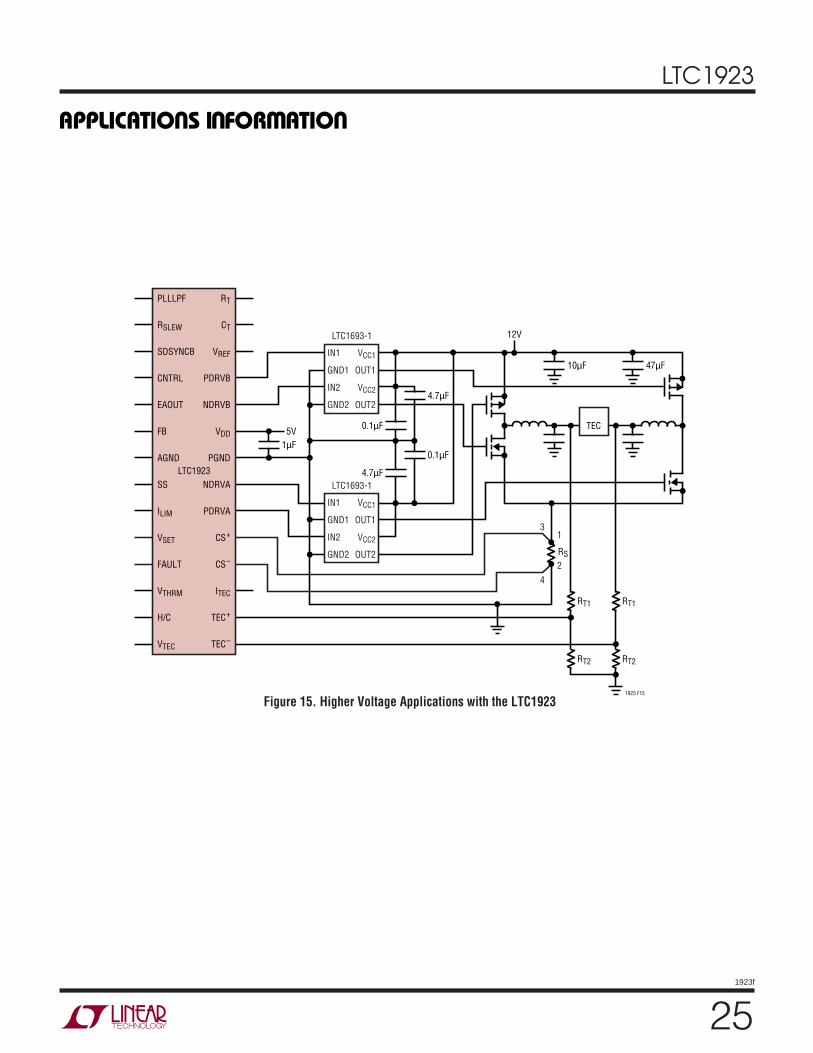
TYPICAL APPLICATIO
U
27
LTC1923
1923f
U
PACKAGE DESCRIPTIO
GN Package28-Lead Plastic SSOP (Narrow .150 Inch)
(Reference LTC DWG # 05-08-1641)
0.386 – 0.393*(9.804 – 9.982)
GN28 (SSOP) 1098
* DIMENSION DOES NOT INCLUDE MOLD FLASH. MOLD FLASHSHALL NOT EXCEED 0.006" (0.152mm) PER SIDE
** DIMENSION DOES NOT INCLUDE INTERLEAD FLASH. INTERLEADFLASH SHALL NOT EXCEED 0.010" (0.254mm) PER SIDE
1 2 3 4 5 6 7 8 9 10 11 12
0.229 – 0.244(5.817 – 6.198)
0.150 – 0.157**(3.810 – 3.988)
202122232425262728 19 18 17
13 14
1615
0.016 – 0.050(0.406 – 1.270)
0.015 ± 0.004(0.38 ± 0.10)
× 45°
0° – 8° TYP0.0075 – 0.0098(0.191 – 0.249)
0.053 – 0.069(1.351 – 1.748)
0.008 – 0.012(0.203 – 0.305)
0.004 – 0.009(0.102 – 0.249)
0.0250(0.635)
BSC
0.033(0.838)
REF
Information furnished by Linear Technology Corporation is believed to be accurate and reliable.However, no responsibility is assumed for its use. Linear Technology Corporation makes no represen-tation that the interconnection of its circuits as described herein will not infringe on existing patent rights.
28
LTC1923
1923f
LINEAR TECHNOLOGY CORPORATION 2001
LT/TP 0502 2K • PRINTED IN USALinear Technology Corporation1630 McCarthy Blvd., Milpitas, CA 95035-7417(408) 432-1900 FAX: (408) 434-0507 www.linear.com
RELATED PARTSPART NUMBER DESCRIPTION COMMENTS
LTC1658 14-Bit Rail-to-Rail Micropower DAC 3V or 5V Single Supply Operation, ICC = 270µA,8-Lead MSOP Package
LTC1693-1 High Speed Dual N-Channel MOSFET Driver 1.5A Peak Output Current, 1GΩ Electrical Isolation, SO-8 Package
LTC2053 Zero Drift Instrumentation Amp Max Gain Error 0.01%, Input Offset Drift of 50nV/°C, Input Offset Voltage of 10µV
U
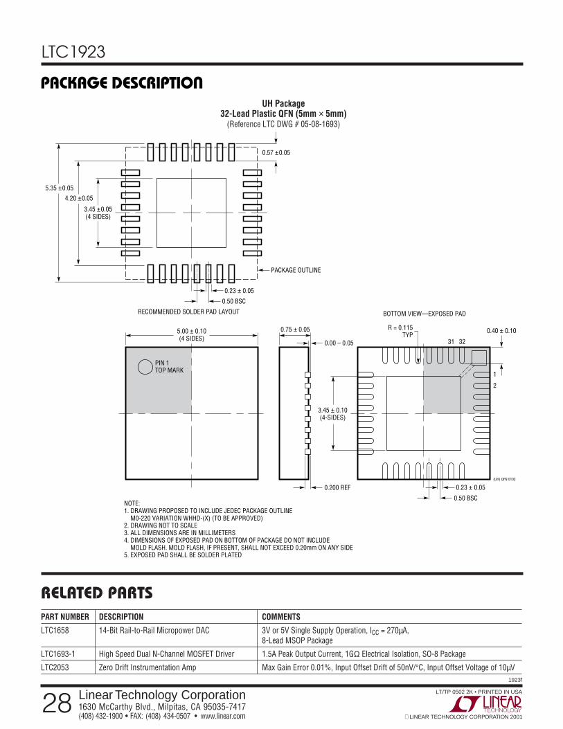
PACKAGE DESCRIPTIO
5.00 ± 0.10(4 SIDES)
NOTE:1. DRAWING PROPOSED TO INCLUDE JEDEC PACKAGE OUTLINE M0-220 VARIATION WHHD-(X) (TO BE APPROVED)2. DRAWING NOT TO SCALE3. ALL DIMENSIONS ARE IN MILLIMETERS4. DIMENSIONS OF EXPOSED PAD ON BOTTOM OF PACKAGE DO NOT INCLUDE MOLD FLASH. MOLD FLASH, IF PRESENT, SHALL NOT EXCEED 0.20mm ON ANY SIDE5. EXPOSED PAD SHALL BE SOLDER PLATED
PIN 1TOP MARK
0.40 ± 0.10
31
1
2
32
BOTTOM VIEW—EXPOSED PAD
3.45 ± 0.10(4-SIDES)
0.75 ± 0.05 R = 0.115TYP
0.23 ± 0.05(UH) QFN 0102
0.50 BSC
0.200 REF
0.00 – 0.05
0.57 ±0.05
3.45 ±0.05(4 SIDES)
4.20 ±0.05
5.35 ±0.05
0.23 ± 0.05
PACKAGE OUTLINE
0.50 BSC
RECOMMENDED SOLDER PAD LAYOUT
UH Package32-Lead Plastic QFN (5mm × 5mm)
(Reference LTC DWG # 05-08-1693)


![In‐situ TEM studies of nanostructured thermoelectric materials: … · cost and high conversion efficiency thermoelectric power generator (TEG).[22–28] Despite those advantages,](https://img.pdfslide.net/doc/110x75/5e37b76cded5da649801e808/inasitu-tem-studies-of-nanostructured-thermoelectric-materials-cost-and-high.jpg)


![CHARACTERISATION OF PERFORMANCES OF ......thermoelectric properties and a high thermoelectric figure of merit zT that correlates directly with the efficiency of the device [1], [2]](https://img.pdfslide.net/doc/110x75/5ff00633263a8c7094610cd6/characterisation-of-performances-of-thermoelectric-properties-and-a-high.jpg)