Embed Size (px)
Citation preview
HIGH EFFICIENCY POWER SUPPLIES FOR MULTI-MODE
RF POWER AMPLIFIERS IN CELLULAR HANDSET
APPLICATIONS
by
Yushan Li
B.S., Peking University, 1990
M.S. in Physics, Institute of High Energy Physics,
Chinese Academy of Sciences, 1993
M.S. in EE, California Institute of Technology, 1995
Electrical Engineer, Columbia University, 2001
A thesis submitted to the
Faculty of the Graduate School of the
University of Colorado in partial fulfillment
of the requirement for the degree of
Doctor of Philosophy
Department of Electrical, Computer and Energy Engineering
2012
This thesis entitled: High Efficiency Power Supplies for Multi-mode RF Power Amplifiers in Cellular Handset
Applications written by Yushan Li
has been approved for the Department of Electrical, Computer and Energy Engineering
________________________________
Dragan Maksimovic
________________________________
Robert Erickson
Date________________
The final copy of this thesis has been examined by the signatories, and we find that both the
content and the form meet acceptable presentation standards of scholarly work in the above
mentioned discipline.

iii
Yushan Li (Ph.D., Electrical, Computer and Energy Engineering)
High Efficiency Power Supplies for Multi-mode RF Power Amplifiers in Cellular Handset Applications
Thesis directed by Professor Dragan Maksimovic
Cellular handset evolution requires the front end transmitter to support multiple 3G/4G bands for
global roaming, and also to be backward compatible with the existing 2G (quad-band GSM/EDGE)
network. The cost and size would be prohibitive if one power amplifier (PA) only supports one band or if
multiple supplies are required for multiple PAs. Solutions of interest are based on multi-standard
multi-band PAs (e.g. 2 multi-mode PAs instead of 8+ mode-specific PAs), and an efficient power supply
that supports these multi-mode PAs.
This thesis addresses efficient power supply solutions for 2G, 3G and 4G PAs, including support
for multi-standard, multi-band PAs. These efficient power supplies have to have wide bandwidth and fast
response times in order to simultaneously meet the time mask and linearity requirements in the GSM/EDGE
and 3G/4G standards. Other important specifications include the GSM/EDGE receiver band noise and full
power control range.
The thesis starts with a study of PA supply architectures and DC-DC converters. A series
architecture consisting of a boost converter followed by a buck converter has advantages of low-noise buck
converter output, together with the ability to deliver full power at low battery voltages to extend the battery
life. The buck converter presents a constant power load for the boost converter, which raises stability
concerns. Small-signal control-to-output transfer functions are derived for peak or valley current mode
controlled boost converter with a downstream regulated converter modeled as constant power load. It is

iv
shown how current mode control provides active damping to ensure stability and well-behaved dynamic
response. Furthermore, it is shown how load current feedforward presents an effective way to improve
power load transient response. Modeling and design approaches are validated by test circuit simulations,
demonstrating stable operations using current mode control under constant power loads, and improved
power step load transient response based on load current feedforward.
A buck/boost and LDO series architecture is proposed as the solution to address efficiency,
linearity, noise and time mask requirements for the supplies supporting multi-standard, multi-band PAs. A
monolithic integrated circuit (IC) has been designed and implemented in a standard 0.5µ, 5V CMOS
process for supplying the multi-mode PAs. The buck/boost converter with wide output range delivers the
peak efficiency of 92%. The power LDO has 1-4 MHz bandwidth, to support the GSM/EDGE/WCDMA
time mask requirements and the polar EDGE operation. The test chip consumes the quiescent current
1.1 mA, and it delivers maximum 5 W output.

v
Acknowledgements
First of all I would like to express sincere gratitude to my advisor, Professor Dragan Maksimovic,
for his strong encouragement and guidance during the course of this work. He has guided me through my
Ph.D. pursuit with his great academic wisdom on the research. It has been one of my most enjoyable
experiences learning from his profound knowledge and expertise.
I must thank my thesis committee members Professor Robert Erickson, Professor Regan Zane,
Professor Zoya Popovic, Professor Y. C. Lee, and Professor Jianliang Xiao for their encouragement and
support.
I acknowledge the generous tuition support from my employer National Semiconductor and now
Texas Instruments for all the years in my Ph.D. program. I would like to thank my colleagues Kevin
Vannorsdel and Art Zirger, and my manager Steve Berg for their technical contribution to my research
and their friendship over the years. I would like to thank Vahid Yousefzadeh and Kirk Garrison for their
evaluation help of the test chip. I would also like to thank Rob Woolf for his continuous support and
encouragement over the years of my Ph.D. program.
I wish to thank my parents who have been supporting and encouraging me to pursue the best
education since my childhood. I would also like to thank my two younger sisters for their love. Finally I
would give my special thanks to my wife, Jie, and my kids, Grace, Mary, John and Phoebe, for their love,
understanding, and patience through years of my long Ph.D. program.

vi
CONTENTS
Chapter 1 Introduction 1
1.1 Introduction 1
1.2 Handset Transmitter Requirements 4
1.2.1 Power Levels 5
1.2.2 Spectrum and Noise in Frequency Domain 6
1.2.3 Transient Response in Time Domain 7
1.3 Thesis Organization 10
Chapter 2 Fundamentals of RF Power Amplifiers and Switching Mode DC/DC Supplies 12
2.1 RF Power Amplifiers 12
2.1.1 Reduced Conduction Angle PAs 13
2.1.2 Harmonic-Tuned PAs 16
2.1.3 Switched-Mode PAs 17
2.1.4 Efficiency Enhancement Architectures 18
2.1.5 Linearity Enhancement Techniques 26
2.2 Inductor-based Switching Mode Power Supplies 27
2.2.1 Buck, Boost and Buck/Boost Switching Converters 27
2.2.2 Voltage Mode and Current Mode Controlled Switching Converters 29
2.2.3 Power Converter Efficiency and Losses 32
2.3 Switching Noise and Spread Spectrum Analysis 33
vii
2.3.1 Buck Converter Switching Noise 33
2.3.2 Boost Converter Switching Noise 34
2.3.3 Noise Reduction using Switching Frequency Dithering 36
Chapter 3 Power Supply Architectures for RF Power Amplifiers 40
3.1 Efficient Power Supply Architectures for RF PAs 40
3.1.1 Buck and Buck/Boost for Average Power Tracking 40
3.1.2 Linear-Assisted-Switcher Topologies 41
3.1.3 Voltage Mode Parallel LAS Architectures 43
3.1.4 Current Mode Parallel LAS Architecture 45
3.1.5 Series LAS Architecture 46
3.2 Architecture Selection 48
3.2.1 Comparison of the Architectures 48
3.2.2 Architecture Choices for Different RF PA Modes 49
3.2.3 Buck/Boost-LDO Series Architecture as Multi-Mode RF PA Supply 50
3.3 Efficient Supply Architectures for High PAR Wideband Systems 51
3.3.1 Parallel/Series ET Architecture 52
3.3.2 Average Power Tracking Supply for Doherty PAs 54
3.3.3 Average Power Tracking Supply for Outphasing PAs 57
3.4 Envelope Tracking for High Power Systems 59
Chapter 4 Stability Control of a Boost Converter Followed by a Buck 65
viii
4.1 Instability Concerns in Converters with Constant Power Loads 65
4.2 Peak Current Mode Control for Boost converters with CPLs 68
4.2.1 Control-to-Output DC Gain Calculation of PCMC Boost Converters with CPLs 68
4.2.2 Control-to-Output Small-Signal Modeling of PCMC Boost Converters with CPLs 70
4.2.3 Load Current Feedforward for PCMC Boost Converters with Resistive Loads 73
4.2.4 Load Current Feedforward for PCMC Boost Converters with CPLs 75
4.3 Valley Current Mode Control for Boost converters with CPLs 76
4.3.1 Control-to-Output DC Gain Calculation of VCMC Boost Converters with CPLs 77
4.3.2 Control-to-Output Small-Signal Modeling of VCMC Boost Converters with CPLs 78
4.3.3 Load Current Feedforward for VCMC Boost Converters with Resistive Loads 80
4.3.4 Load Current Feedforward for VCMC Boost Converters with CPLs 80
4.4 Simulation Results 80
4.5 Summary 86
Chapter 5 Multi-Mode RF PA Supply Design 87
5.1 Buck/Boost Converter 88
5.1.1 Buck or Boost PWM 88
5.1.2 Error Amplifier 92
5.1.3 Oscillator 97
5.1.4 Current Limit and Current Sensing Blocks 99
5.1.5 Output Switches and Driver 101
ix
5.2 Wideband VCC LDO 103
5.3 PA Bias Generator 111
5.4 Experimental Results for the Multi-Mode RF PA Supply 113
5.4.1 Experimental Results of the Buck/Boost Switcher 113
5.4.2 Experimental Results of the Main and Bias LDOs 117
5.4.3 Experimental Results for the Multi-Mode Supply with RF PA 119
Chapter 6 Conclusions 123
6.1 Thesis Summary 123
6.2 Future Directions 126
References 128
Appendix A Bandgap Reference Cell Small-Signal and Process Variation Analysis 137
A.1 Bandgap Reference Small-Signal Model 138
A.2 Bandgap Reference Process Variation 139
x
Tables
Table 1.1: Standards comparison of concerned parameters for handset transmitters............................................ 3
Table 1.2: EDGE 8-PSK EVM specifications for handsets .................................................................................. 6
Table 1.3: WCDMA handsets ACLR requirements .............................................................................................. 7
Table 1.4: Handset transmitter PA supply related key requirements ..................................................................... 9
Table 2.1: DC/DC converter conversion ratio..................................................................................................... 29
Table 2.2: DC/DC converter transfer function in CCM ...................................................................................... 31
Table 2.3: DC/DC converter transfer function in DCM ...................................................................................... 32
Table 3.1: PA supply architecture comparison .................................................................................................... 48
Table 4.1: CMC boost control-to-output small-signal model with resistive loads ...................................... 82
Table 4.2: CMC boost control-to-output small-signal model with constant power loads ........................... 83
Table 5.1: Buck and Boost mixing to achieve equivalent Buck or Boost ........................................................... 90
Table 5.2: Quiescent current of various circuit blocks ...................................................................................... 122
Table 5.3: Key parameters of the multi-mode PA supply.................................................................................. 122

xi
Figures
Figure 1-1: Handset transmitters with multiple mode operations (GSM/EDGE/WCDMA). ............................... 4
Figure 1-2: PDF of GSM and WCDMA handset output power. ........................................................................... 6
Figure 1-3: Modulation spectral mask for GMSK/8-PSK. ................................................................................... 7
Figure 1-4: GSM time mask. ................................................................................................................................ 8
Figure 1-5: WCDMA transmit template requirements. ......................................................................................... 9
Figure 2-1: Block diagram of a general PA. ....................................................................................................... 12
Figure 2-2: PA transistor voltage and current waveforms in different classes. ................................................... 14
Figure 2-3: Theoretic efficiency and relative power for reduced conduction angle modes of operation. ........... 15
Figure 2-4: Class-A and class-B PA theoretic efficiency vs relative output power. ............................................ 16
Figure 2-5: Block diagram of a class-E PA. ........................................................................................................ 17
Figure 2-6: Block diagram of a PA with EER. .................................................................................................... 19
Figure 2-7: Block diagram of a PA with ET. ....................................................................................................... 20
Figure 2-8: PA load line change with average power tracking from dynamic supply (DVB) and/or dynamic
current bias (DCB). ............................................................................................................................................. 21
Figure 2-9: Block diagram of a Doherty PA. ...................................................................................................... 22
Figure 2-10: Block diagram of a out-phasing PA. .............................................................................................. 24
Figure 2-11: Representative PA efficiency vs its output envelop for different techniques [40]. ......................... 25
Figure 2-12: Block diagram of a typical transmitter configuration with DPD. .................................................. 26
Figure 2-13: Block diagram of a typical polar transmitter configuration with closed-loop feedback. ............... 27
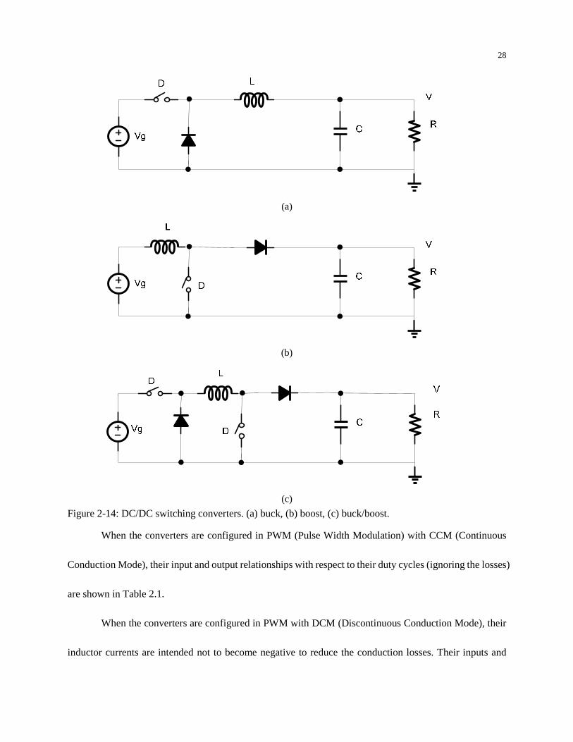
Figure 2-14: DC/DC switching converters. (a) buck, (b) boost, (c) buck/boost. ................................................ 28
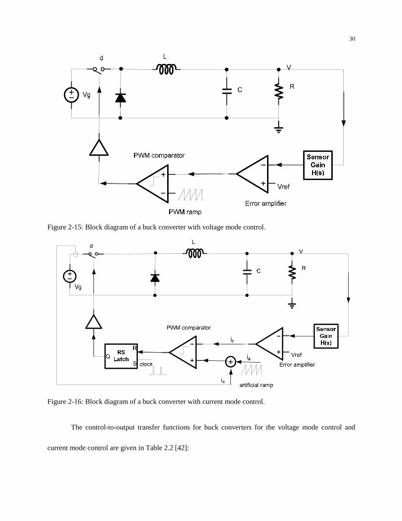
Figure 2-15: Block diagram of a buck converter with voltage mode control. .................................................... 30
Figure 2-16: Block diagram of a buck converter with current mode control. ..................................................... 30
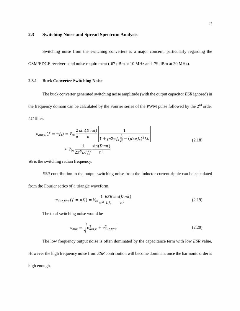
Figure 2-17: Buck and boost switching noise at different switching harmonics from ESR and capacitance
contributions. ...................................................................................................................................................... 36
Figure 2-18: Switching noise reduction from switching frequency modulation with respective to RSW. ......... 39
Figure 3-1: A boost converter followed by a buck converter for APT. ............................................................... 41
Figure 3-2: Block diagram for a parallel LAS. ................................................................................................... 42
Figure 3-3: Block diagram of a series LAS. ....................................................................................................... 42
Figure 3-4: Block diagram of a parallel/series LAS. .......................................................................................... 42
Figure 3-5: Block diagram of a voltage mode parallel LAS with AC coupling. ................................................. 44
Figure 3-6: Block diagram of a voltage mode parallel LAS with a dead-zone linear amplifier. ........................ 45
Figure 3-7: Block diagram of a current mode parallel LAS architecture ............................................................ 46
Figure 3-8: Block diagram of a series LAS architecture. .................................................................................... 47
Figure 3-9: Block diagram of parallel/series envelope tracking architecture. .................................................... 53
Figure 3-10: Block diagram of a Doherty PA with APT from dynamic supply and dynamic bias. .................... 57
Figure 3-11: Block diagram of an outphasing PA with APT from dynamic supply. ........................................... 59
Figure 3-12: Block diagram of a parallel LAS architecture with nested current mode control. ......................... 61
Figure 3-13: Simulated current waveforms of a parallel LAS architecture with nested current mode control. .. 62
Figure 3-14: Block diagram of a parallel LAS architecture with class-H linear amplifier. ................................ 63

xii
Figure 3-15: Simulated waveforms of a parallel LAS architecture with class-H linear amplifier. ..................... 64
Figure 4-1: (a) A boost converter is loaded with constant power load. (b) Constant power load model (power
sink) and small-signal model (negative resistor). (c) Passive compensation for the boost converter with
constant power load. ........................................................................................................................................... 66
Figure 4-2: Block diagram of a boost converter with peak current model control (PCMC). .............................. 69
Figure 4-3: Graphic representation of the steady state control-to-duty cycle of a PCMC boost converter under a
CPL. (a) without slope compensation. (b) with slope compensation. ................................................................. 69
Figure 4-4: Small-signal block diagram of a boost converter with current model control and load current
feedforward. ........................................................................................................................................................ 71
Figure 4-5: Block diagram of a boost converter with PWM valley current model control. ................................ 77
Figure 4-6: Graphic representation of the steady state control-to-duty cycle of a VCMC boost converter under a
CPL. (a) without slope compensation. (b) with slope compensation. ................................................................. 77
Figure 4-7: Modeled and simulated response of a boost convert with PCMC under CPLs. (a) Modeled and
simulated small-signal frequency response without load current feedforward. (b) Modeled and simulated
small-signal frequency response with load current feedforward. ....................................................................... 84
Figure 4-8: Modeled and simulated response of a boost convert with VCMC under CPLs. (a) Modeled and
simulated small-signal frequency response without load current feedforward. (b) Modeled and simulated
small-signal frequency response with load current feedforward. ....................................................................... 84
Figure 4-9: Simulated load step transient responses simulated response of a boost convert under CPLs.
(a) PCMC. (b) VCMC...................................................................................................................................... 85
Figure 5-1: Block diagram of a multi-mode PA supply with series LAS architecture. ....................................... 87
Figure 5-2: A buck or boost architecture with voltage mode control sharing a single error amplifier. ............... 89
Figure 5-3: Buck or boost architecture with out-of-phase triangle waveforms as PWM ramps. ........................ 91
Figure 5-4: PWM waveforms to illustrate the buck and boost mixing in the transition region. ......................... 92
Figure 5-5: Small signal block diagram of a buck/boost converter with voltage mode control. ........................ 93
Figure 5-6: Buck/boost error amplifier architecture. .......................................................................................... 94
Figure 5-7: Loop gain bode plot of the buck/boost converter in boost, and buck CCM and DCM operations. . 96
Figure 5-8: Block diagram of a out-of-phase triangle waveform generator with controlled center voltage. ...... 98
Figure 5-9: An oscillator to control the switching frequency dithering. ............................................................. 99
Figure 5-10: A current limit comparator for a buck converter. ......................................................................... 100
Figure 5-11: Current sensing amplifier for a buck converter. ........................................................................... 101
Figure 5-12: VCC LDO architecture with parallel PMOS and NMOS output. (a) LDO architecture, (b) LDO
control amplifier. ............................................................................................................................................... 105
Figure 5-13: Loop gain Bode plot of the VCC amplifier with output PMOS or NMOS under control. ........... 106
Figure 5-14: VCC amplifier with smooth transition between the output PMOS and NMOS control loops. .... 107
Figure 5-15: LDO waveforms of LDO architecture with switched PMOS and NMOS control loop. The glitches
can be seen from the PMOS and NMOS gates and the output during the loop transition. ............................... 108
Figure 5-16: LDO waveforms of LDO architecture with smooth PMOS and NMOS control loop transition.
No glitches can be seen from the PMOS and NMOS gates and the output during the loop transition. ............ 109
Figure 5-17: LDO loop gain bode plot when NMOS is active. ........................................................................ 110
Figure 5-18: Simulated waveforms of output tracking response to a polar EDGE reference. .......................... 111

xiii
Figure 5-19: PA bias generation with two outputs being independently regulated. .......................................... 112
Figure 5-20: Die microphotograph of the test chip. .......................................................................................... 113
Figure 5-21: Boost steady state switching waveforms. ..................................................................................... 114
Figure 5-22: Buck/boost load transient response .............................................................................................. 115
Figure 5-23: Buck and boost transition control comparison ............................................................................. 116
Figure 5-24: Measured buck/boost converter efficiency under different output voltage and load current. ...... 117
Figure 5-25: LDO reference triangle tracking. ................................................................................................. 118
Figure 5-26: Startup response of PA bias outpout. ............................................................................................ 118
Figure 5-27: Combined efficiency of PA with the multi-mode supply. ............................................................ 120
Figure 5-28: GSM PA output receiver band noise comparison. ........................................................................ 121
Figure A-1: A bandgap reference. ..................................................................................................................... 138
Figure A-2: Small-signal model of the bandgap reference. .............................................................................. 139
Figure A-3: Small-signal model of the bandgap reference with amplifier offset. ............................................. 140
Figure A-4: Small-signal model of the bandgap reference with resistor mismatching. .................................... 141
Figure A-5: Folded cascode amplifier for bandgap reference. .......................................................................... 143
Figure A-6: A bandgap reference with current mirror. ...................................................................................... 145
1
Chapter 1
Introduction
1.1 Introduction
The wireless communication standards have been evolving to meet the demands for higher data
rates and more functionality. Consequently, mobile handsets are more and more power hungry. As radio
frequency (RF) power amplifiers (PAs) consume significant amount of power among all the components in
the handsets, it becomes increasingly important to improve the PA efficiency. This thesis is intended to
address the question of how to improve the overall transmitter efficiency from the PA supply point of view.
Efficient dynamic supplies using switching DC/DC converters are very common nowadays for
3G/3.5G WCDMA/HSPA1 PAs. However linear regulators or low dropout linear regulators (LDOs) are
still the predominant supplies for the 2G/2.75G GSM/EDGE PAs due to their stringent receiver band noise
and time mask system requirements [1]. The LDO supply has low efficiency when the GSM/EDGE PA
power is backed off from the peak. There has been a lot of research work published on the PA efficiency
improvement for the EDGE systems. One popular architecture solution to improve the EDGE PA efficiency
is through polar modulation [2]-[14]. Wide bandwidth switching buck converters have been proposed for
1 WCDMA and HSPA stand for Wideband Code Division Multiple Access, and High Speed Packet Access respectively. WCDMA is
the air interface for UMTS (Universal Mobile Telecommunications System). HSPA is collection of HSDPA (High Speed Downlink Packet Access)
and HSUPA (High Speed Uplink Packet Access), which were defined in the UMTS Release 5 and Release 6 respectively. HSPA+ (Evolved HSPA),
defined in the UMTS Release 7 and Release 8, allows 2-carrier HSDPA and 2-carrier HSUPA. UMTS, HSPA and HSPA+ are often considered as
3G, 3.5G and 3.75G respectively.
2
the EDGE polar modulation PAs [3]-[14]. An envelope modulator is implemented using 4.3 MHz buck
converter in [4]-[5]. In [8]-[11], the parallel hybrid architecture of a switcher with a linear amplifier is
implemented for the polar EDGE transmitter. In [12], a series architecture of a buck converter with a linear
regulator is implemented. In [13], a 10 MHz 4-switch buck boost converter is implemented, however the
spectral noise in the boost mode is larger than the EDGE standard requirement. In [14], a two-stage
converter is implemented with the 1st stage of a switching capacitor charge pump doubler and followed by
a 10 MHz buck converter. It is much more difficult to apply the DC/DC boost converter for the EDGE polar
PAs due to the much higher switching noise in the boost converter [13].
Cellular handset evolution requires the front end transmitter to support multiple bands for global
roaming, and also to be backward compatible with the existing quad-band 2G/2.75G (GSM/EDGE)
network. 3G/3.5G WCDMA/HSPA and 4G LTE2 are typically used for the high speed data service, and
GSM/EDGE are typically used for the voice and low-rate data service. Table 1 compares a few key
parameters for the different standards of the cellular handset transmitters [15]. The power amplifier (PA)
manufactures are rolling out the multi-mode, multi-band PAs [16]-[17]. Recently a multi-mode PA supply
has been commercially introduced along with the multi-mode, multi-band PAs although details are
unknown [18]. Another advantage of the multi-mode transmitters is related to the concept of Software
Defined Radio (SDR). SDR attempts to use software to program the same radio hardware so that the
hardware can work for different wireless standards and even for future standards. On the other hand, the
2 LTE stands for Long Term Evolution. LTE is considered as 3.9G. LTE Advanced is currently standardized
as 4G. WiMAX (Worldwide Interoperability for Microwave Access) is based on the IEEE 802.16 standard. The IEEE
802.16m is under development to fulfill the 4G requirement. Both LTE and WiMAX use OFDM (Orthogonal
Frequency Division Multiplexing) for high data rate.
3
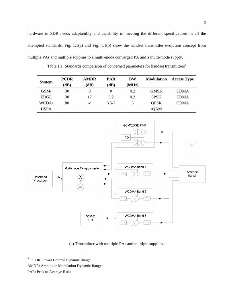
hardware in SDR needs adaptability and capability of meeting the different specifications in all the
attempted standards. Fig. 1.1(a) and Fig. 1.1(b) show the handset transmitter evolution concept from
multiple PAs and multiple supplies to a multi-mode converged PA and a multi-mode supply.
Table 1.1: Standards comparison of concerned parameters for handset transmitters3
System PCDR (dB)
AMDR (dB)
PAR (dB)
BW (MHz)
Modulation Access Type
GSM/ 30 0 0 0.2 GMSK TDMA
EDGE 30 17 3.2 0.2 8PSK TDMA
WCDA/
HSPA
80 ∞ 3.5-7 5 QPSK
/QAM
CDMA
(a) Transmitter with multiple PAs and multiple supplies.
3 PCDR: Power Control Dynamic Range;
AMDR: Amplitude Modulation Dynamic Range;
PAR: Peak to Average Ratio
4
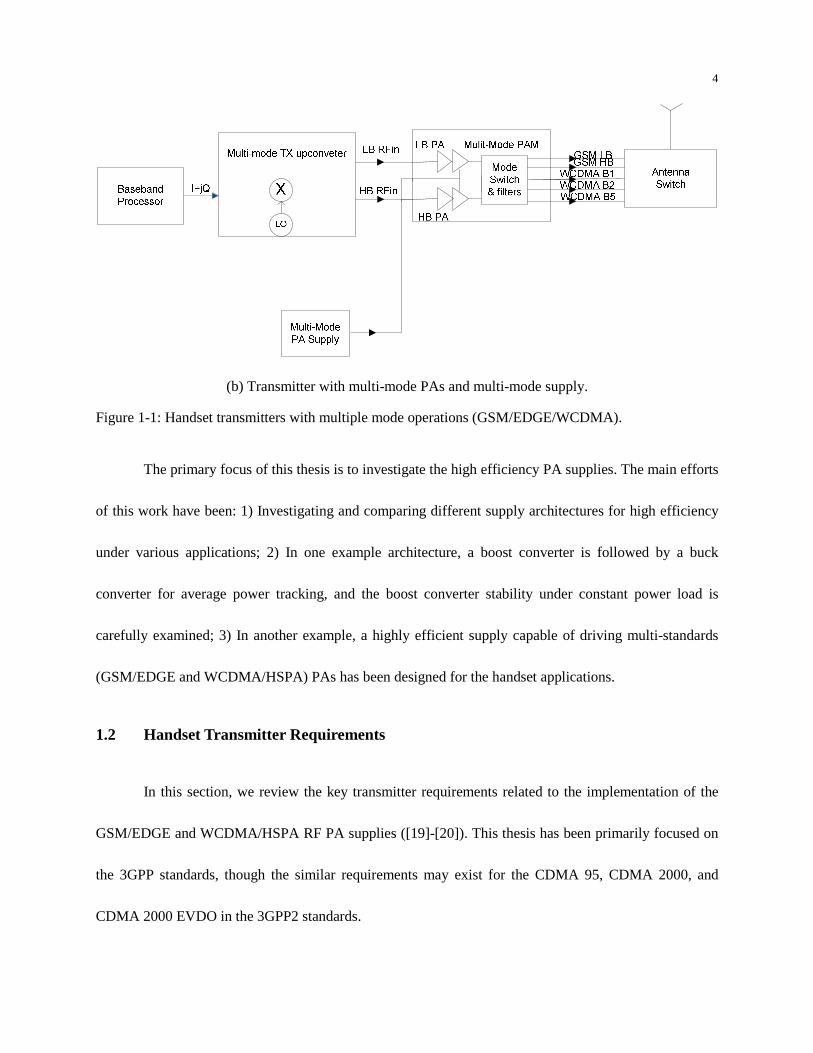
(b) Transmitter with multi-mode PAs and multi-mode supply.
Figure 1-1: Handset transmitters with multiple mode operations (GSM/EDGE/WCDMA).
The primary focus of this thesis is to investigate the high efficiency PA supplies. The main efforts
of this work have been: 1) Investigating and comparing different supply architectures for high efficiency
under various applications; 2) In one example architecture, a boost converter is followed by a buck
converter for average power tracking, and the boost converter stability under constant power load is
carefully examined; 3) In another example, a highly efficient supply capable of driving multi-standards
(GSM/EDGE and WCDMA/HSPA) PAs has been designed for the handset applications.
1.2 Handset Transmitter Requirements
In this section, we review the key transmitter requirements related to the implementation of the
GSM/EDGE and WCDMA/HSPA RF PA supplies ([19]-[20]). This thesis has been primarily focused on
the 3GPP standards, though the similar requirements may exist for the CDMA 95, CDMA 2000, and
CDMA 2000 EVDO in the 3GPP2 standards.
5
1.2.1 Power Levels
The output power control ranges for GSM, EDGE and WCDMA/HSPA are very different. GSM
(Class-4 GSM850/900) requires the maximum output power at antenna of 33 dBm. The minimum
controlled output power is 0 dBm. EDGE requires the maximum output power of 27 dBm (Class-E2), and
the minimum of 0 dBm. WCDMA/HSPA requires the maximum output power of 24 dBm (Class-3), and the
minimum of -50 dBm (or 10 nW).
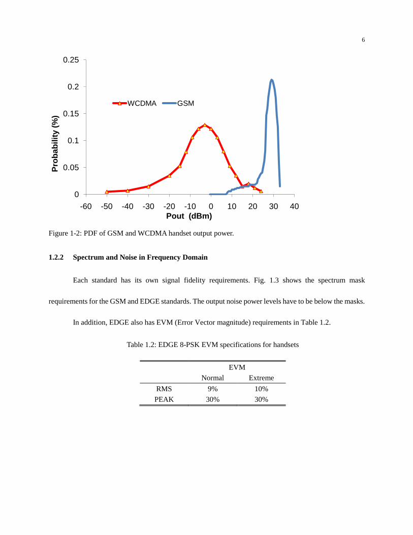
The PDF (Probability Density Function) of the average power distribution is shown in Fig. 1.2 for a
majority of WCDMA handsets in the voice mode [21]. The power level of the maximum probability is
around -2 dBm (or 0.6 mW). In the HSPA data mode, the power level of the maximum probability is shifted
roughly about 10 dB higher than in the voice mode. The PDF for GSM handset output power is very
different [22], also shown in Fig. 1.2. The power level of the GSM maximum probability is around 30 dBm,
near its maximum output power level, though the maximum probability may be shifted to much lower
power level in metropolitan areas. This requires the multi-mode PA supply to be efficient for both very high
and very low power levels. The average usage efficiency can be calculated based on the PDF and is given
below in (1.1).
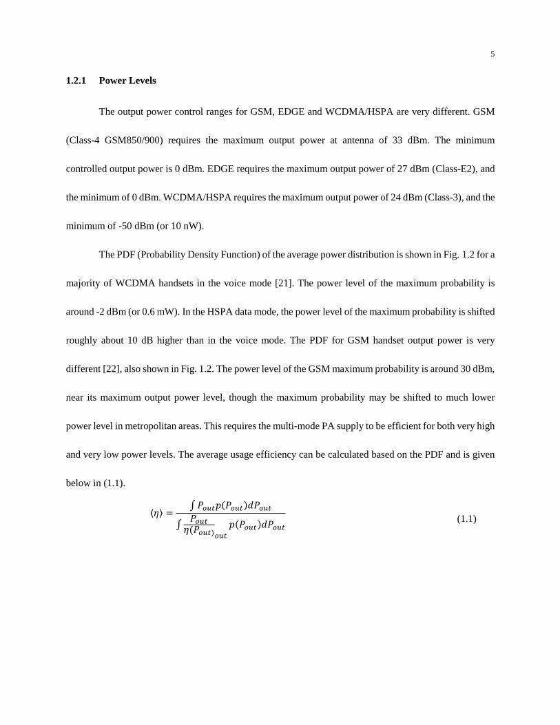
(1.1)
6
Figure 1-2: PDF of GSM and WCDMA handset output power.
1.2.2 Spectrum and Noise in Frequency Domain
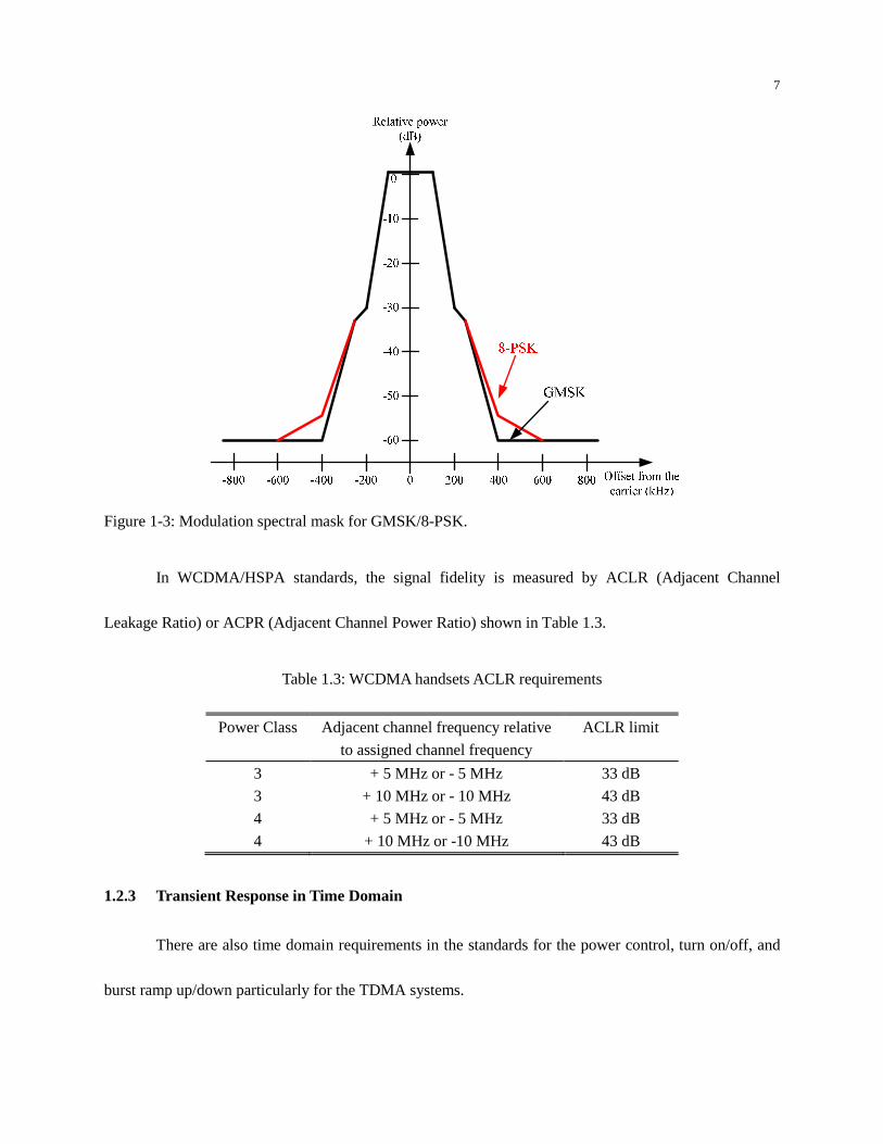
Each standard has its own signal fidelity requirements. Fig. 1.3 shows the spectrum mask
requirements for the GSM and EDGE standards. The output noise power levels have to be below the masks.
In addition, EDGE also has EVM (Error Vector magnitude) requirements in Table 1.2.
0
0.05
0.1
0.15
0.2
0.25
-60 -50 -40 -30 -20 -10 0 10 20 30 40
Pro
bab
ility
(%
)
Pout (dBm)
WCDMA GSM
Table 1.2: EDGE 8-PSK EVM specifications for handsets
EVM
Normal Extreme
RMS 9% 10%
PEAK 30% 30%
7
Figure 1-3: Modulation spectral mask for GMSK/8-PSK.
In WCDMA/HSPA standards, the signal fidelity is measured by ACLR (Adjacent Channel
Leakage Ratio) or ACPR (Adjacent Channel Power Ratio) shown in Table 1.3.
Table 1.3: WCDMA handsets ACLR requirements
Power Class Adjacent channel frequency relative
to assigned channel frequency
ACLR limit
3 + 5 MHz or - 5 MHz 33 dB
3 + 10 MHz or - 10 MHz 43 dB
4 + 5 MHz or - 5 MHz 33 dB
4 + 10 MHz or -10 MHz 43 dB
1.2.3 Transient Response in Time Domain
There are also time domain requirements in the standards for the power control, turn on/off, and
burst ramp up/down particularly for the TDMA systems.
8
The average power control is generally very slow compared with the power supply bandwidth. In
GSM/EDGE, it is at a rate of one nominal 2 dB power control step every 60 ms. In WCDMA/HSPA, the
closed-loop power control rate is in the range of 1.5 kHz.
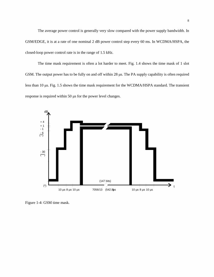
The time mask requirement is often a lot harder to meet. Fig. 1.4 shows the time mask of 1 slot
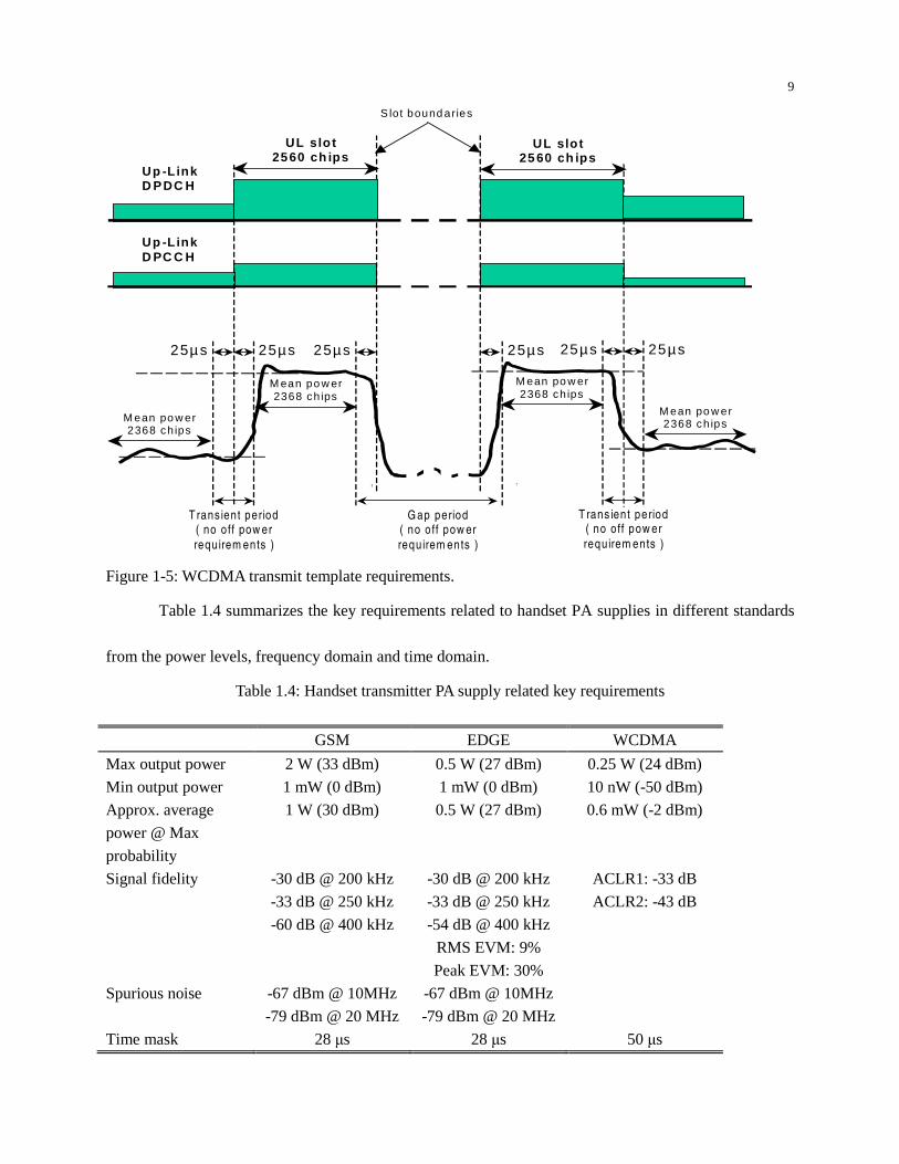
GSM. The output power has to be fully on and off within 28 µs. The PA supply capability is often required
less than 10 µs. Fig. 1.5 shows the time mask requirement for the WCDMA/HSPA standard. The transient
response is required within 50 µs for the power level changes.
Figure 1-4: GSM time mask.
dB
t
- 6
- 30
+ 4
8 µs 10 µs 10 µs 8 µs
(147 bits)
7056/13 (542.8)µs 10 µs(*)
10 µs
- 1 + 1
( * ** )
( * * )
9
S lot bound aries
Up -Link D PDC H
M ean po w er 2368 ch ips
25µ s
Up -Link D PC C H
M ean po w er 2368 ch ips
M ean po w er 2368 ch ips
25µ s
25µ s
T rans ient period ( no o ff pow er
requ irem ents )
UL slot 25 60 ch ips
UL slot 2560 ch ips
25µ s
G ap period ( no o ff pow er
requ irem ents )
25µ s
25µ s
T rans ient period ( no o ff pow er
requ irem ents )
M ean po w er 2368 ch ips
Figure 1-5: WCDMA transmit template requirements.
Table 1.4 summarizes the key requirements related to handset PA supplies in different standards
from the power levels, frequency domain and time domain.
Table 1.4: Handset transmitter PA supply related key requirements
GSM EDGE WCDMA
Max output power 2 W (33 dBm) 0.5 W (27 dBm) 0.25 W (24 dBm)
Min output power 1 mW (0 dBm) 1 mW (0 dBm) 10 nW (-50 dBm)
Approx. average
power @ Max
probability
1 W (30 dBm) 0.5 W (27 dBm) 0.6 mW (-2 dBm)
Signal fidelity -30 dB @ 200 kHz
-33 dB @ 250 kHz
-60 dB @ 400 kHz
-30 dB @ 200 kHz
-33 dB @ 250 kHz
-54 dB @ 400 kHz
RMS EVM: 9%
Peak EVM: 30%
ACLR1: -33 dB
ACLR2: -43 dB
Spurious noise -67 dBm @ 10MHz
-79 dBm @ 20 MHz
-67 dBm @ 10MHz
-79 dBm @ 20 MHz
Time mask 28 µs 28 µs 50 µs
10
If the switching converter for the WCDMA/HSPA PAs can also be shared for the GSM/EDGE PAs,
the backoff efficiency would be improved as well. However the supplies for the WCDMA PAs and for the
GSM/EDGE PAs have very different requirements due to the system difference. For example it is very
challenging to meet the GSM/EDGE time mask (< 28 µs from minimum power to maximum power or
vice-versa) and receiver band noise requirements when the switching DC/DC (particularly boost) converter
is used. Another important aspect for the multi-mode supply efficiency optimization is the statistical power
probability distribution difference for the WCDMA and GSM/EDGE systems. The highest probability for
the GSM/EDGE systems is near its peak level, while the highest probability for the WCDMA systems is at
very low level (near -2 dBm in the urban areas). The integrated multi-mode supply needs to be efficient for
both high and low power levels.
1.3 Thesis Organization
Following the introductory chapter which briefly describes the motivation of the work and the
multi-standard system requirements, the thesis material is developed in detail in five additional chapters.
In Chapter 2, the background about RF PAs and switching mode power supplies (SMPS) is briefly
reviewed. Switching noise and the spread spectrum by switching frequency dithering are also analyzed.
In Chapter 3, a few candidate linear assisted switcher (LAS) architectures are studied and compared
for the RF PA supply applications. Three architectures are proposed for the high PAR wideband systems
such as LTE and WiMAX. A nested parallel LAS architecture and a class-H linear amplifier are proposed
for the high power applications.
In Chapter 4, the stability issue of a boost converter when followed by a buck is investigated. The
11
series architecture is a simple form for the power tracking applications. Since the high efficiency buck
presents a constant power load to the upstream boost converter, the stability issue related to the negative
resistance can be very challenging. Current-model-control (CML) turns out to be an effective way to
address the stability problem as an active damping approach. Detailed modeling and analysis are presented.
Load current feedforward for transient response improvement has also been analyzed. Simulation results
match well with the model predictions.
In Chapter 5, the buck/boost and LDO series architecture is proposed for the multi-mode PA supply.
The design and implementation details of the architecture are described. The buck and boost duty cycle
dithering technique is described to eliminate the sub-harmonic behavior in the high buck and low boost duty
cycles conditions. The error amplifier capable of the multiple operation modes is also described. The error
amplifier is shared in the different operation modes, and yet it is compensated differently for the different
modes. The wideband LDO has wide input range, requiring two parallel output PMOS and NMOS devices.
Again the two control loops share the same error amplifier and are compensated properly in both conditions.
Design of other peripheral blocks (such as oscillator and current limit) is also described.
Experimental verification results of the test chip are included in Chapter 5. The verifications were
conducted in two levels: the standalone IC and with the RF PA. High system efficiency is demonstrated.
Finally the thesis is concluded in Chapter 6 with the key contributions reviewed and future
directions proposed.
12
Chapter 2
Fundamentals of RF Power Amplifiers and Switching Mode DC/DC
Supplies
In this chapter, the fundamentals of the RF PAs and switching mode power supplies (SMPS) are
briefly reviewed in Section 2.1 and 2.2, respectively. The switching noise and the spread spectrum are
analyzed in Section 2.3.
2.1 RF Power Amplifiers
Fig. 2.1 shows the basic block diagram of a RF PA. For the handset applications, GaAs HBT
(Hetero-junction Bipolar Transistor) is the technology most often used.
Figure 2-1: Block diagram of a general PA.
PA collector , PAE (power-added efficiency), and overall efficiency have the flowing
13
relationships with respect to the PA power gain .
(2.1)
(2.2)
1 1 (2.3)
1 (2.4)
2.1.1 Reduced Conduction Angle PAs
RF PAs are classically categorized into different modes according to the conduction angles of their
amplification transistors, shown in Fig. 2.2. Class-A PA transistor conducts during the whole cycle with
360°. Class-B PA transistor conducts during the half cycle with 180°. The Class-AB conduct angle is
between 180° and 360°. The conducting angle less than 180° is named Class-C. Class-A and Class-B PAs
are linear, and Class-AB and Class-C PAs are non-linear, though Class-AB is often considered linear for
practical applications.
14
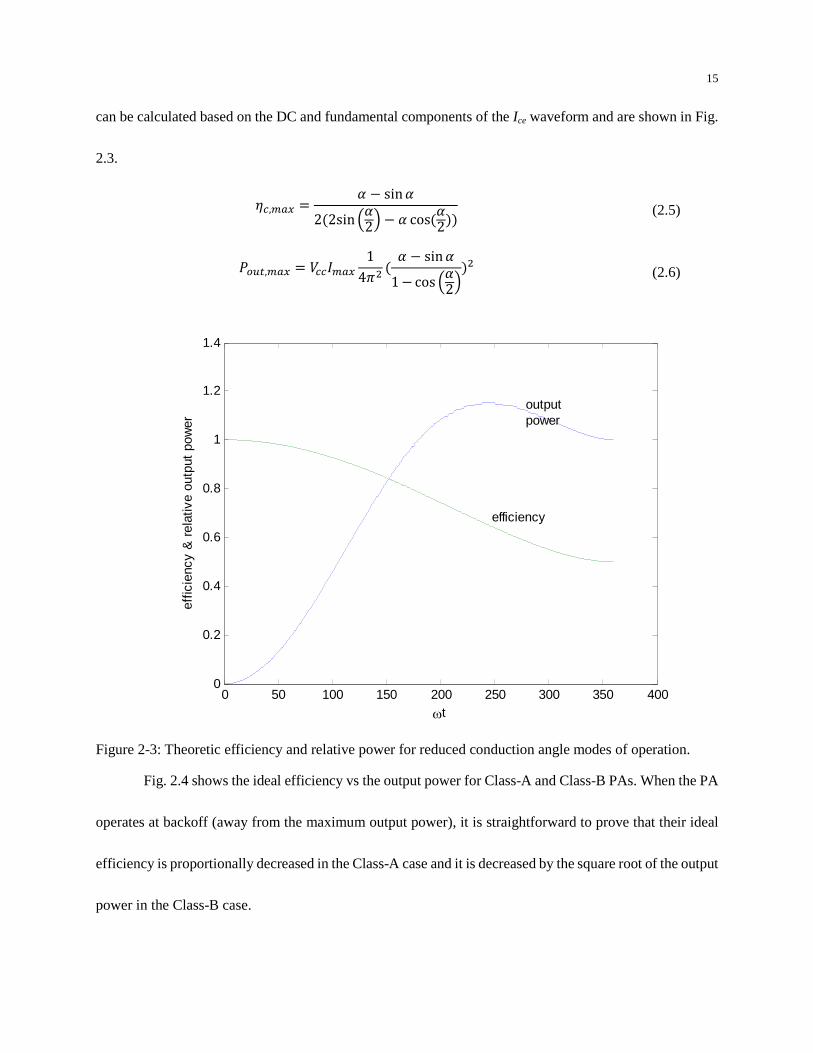
Figure 2-2: PA transistor voltage and current waveforms in different classes.
The PA maximum collector efficiency and the maximum output power with the conduction angle α
0 100 200 300 4000
0.5
1Ice
0 100 200 300 4000
1
2Vce (normalized to Vcc)
0 100 200 300 4000
0.5
1
0 100 200 300 4000
1
2
0 100 200 300 4000
0.5
1
0 100 200 300 4000
1
2
0 100 200 300 4000
2
4
0 100 200 300 4000
0.5
1
ωt0 100 200 300 400
-2
0
2
ωt
0 100 200 300 4000
0.5
1
A
B
C
E
F
15
can be calculated based on the DC and fundamental components of the Ice waveform and are shown in Fig.
2.3.
, sin 22sin $2% cos2 (2.5)
, () 14+, sin 1 cos $2%, (2.6)
Figure 2-3: Theoretic efficiency and relative power for reduced conduction angle modes of operation.
Fig. 2.4 shows the ideal efficiency vs the output power for Class-A and Class-B PAs. When the PA
operates at backoff (away from the maximum output power), it is straightforward to prove that their ideal
efficiency is proportionally decreased in the Class-A case and it is decreased by the square root of the output
power in the Class-B case.
0 50 100 150 200 250 300 350 4000
0.2
0.4
0.6
0.8
1
1.2
1.4
ωt
effic
ienc
y &
rel
ativ
e ou
tput
pow
er
outputpower
efficiency
16
Figure 2-4: Class-A and class-B PA theoretic efficiency vs relative output power.
2.1.2 Harmonic-Tuned PAs
There are other classes of RF PAs considered in the category of harmonic-tuned PAs ([23]-[24]),
including Class-F, Class-F-1, and Class-J. In these PAs, the transistor voltage and current waveforms are
shaped in specific ways to reduce the voltage and current overlap to achieve high efficiency. In Class-F, the
transistor voltage is shaped as a square-wave, with even harmonics terminated with short circuit, and odd
harmonics are terminated with open circuit. In Class- F-1, the transistor current is shaped as a square-wave,
with even harmonics terminated with short circuit, and odd harmonics are terminated with open circuit. In
Class-J, the transistor output shunt capacitance may be used to terminate the harmonics. Class-F, Class-F-1
and Class-J are considered the extension of overdriven Class-AB.
0 0.1 0.2 0.3 0.4 0.5 0.6 0.7 0.8 0.9 10
0.1
0.2
0.3
0.4
0.5
0.6
0.7
0.8
normalized output power
idea
l eff
icie
ncy
Class A
Class B
17
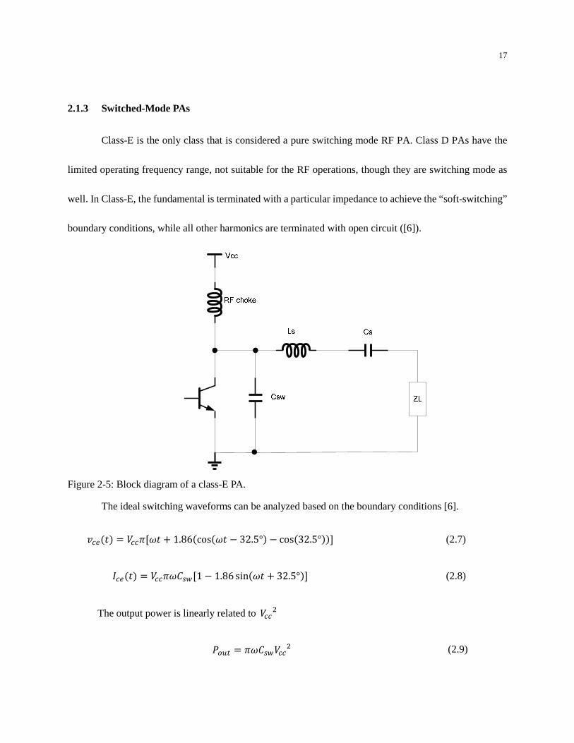
2.1.3 Switched-Mode PAs
Class-E is the only class that is considered a pure switching mode RF PA. Class D PAs have the
limited operating frequency range, not suitable for the RF operations, though they are switching mode as
well. In Class-E, the fundamental is terminated with a particular impedance to achieve the “soft-switching”
boundary conditions, while all other harmonics are terminated with open circuit ([6]).
Figure 2-5: Block diagram of a class-E PA.
The ideal switching waveforms can be analyzed based on the boundary conditions [6].
-. (+/0. 1.86cos0. 32.5° cos32.5°7 (2.7)
)-. (+089:/1 1.86 sin0. 32.5°7 (2.8)
The output power is linearly related to (,
+089:(, (2.9)

18
2.1.4 Efficiency Enhancement Architectures
There are a number of architectures having been extensively studied to enhance the PA efficiency.
• EER
The EER (Envelope Elimination and Restoration) technique was introduced by Kahn [25], and it is
also called the Kahn technique. In this architecture (Fig. 2.6), the RF PA itself is assumed a high efficiency
non-linear PA. The linearization of the PA is from its power supply. The RF input has constant envelope
and only contains the phase information. The signal amplitude (envelope) information is provided from the
PA supply. So the technique is also called polar modulation as opposed to the quadrature modulation. It is a
technique to linearize an efficient non-linear PA. The overall efficiency is the product of the PA efficiency
and the PA supply efficiency.
Ideally an efficient Class-E PA may be used for EER. Class-E PA has the linear relationship
between the collector/drain bias and the output signal amplitude [6]. However the feed-through issue at low
signal levels often requires the predistortion technique to improve the linearity. EER has been popular for
the EDGE standard due to its relatively low signal bandwidth requirement. A special form of EER is the
amplitude information being contained in the PA base/gate control through polar loop [2] instead of the PA
supply, however the efficiency improvement potential is more limited than the supply EER.
19
Figure 2-6: Block diagram of a PA with EER.
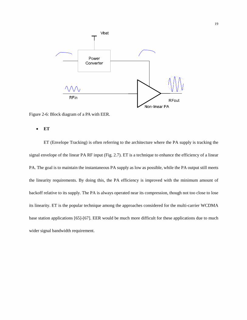
• ET
ET (Envelope Tracking) is often referring to the architecture where the PA supply is tracking the
signal envelope of the linear PA RF input (Fig. 2.7). ET is a technique to enhance the efficiency of a linear
PA. The goal is to maintain the instantaneous PA supply as low as possible, while the PA output still meets
the linearity requirements. By doing this, the PA efficiency is improved with the minimum amount of
backoff relative to its supply. The PA is always operated near its compression, though not too close to lose
its linearity. ET is the popular technique among the approaches considered for the multi-carrier WCDMA
base station applications [65]-[67]. EER would be much more difficult for these applications due to much
wider signal bandwidth requirement.
20
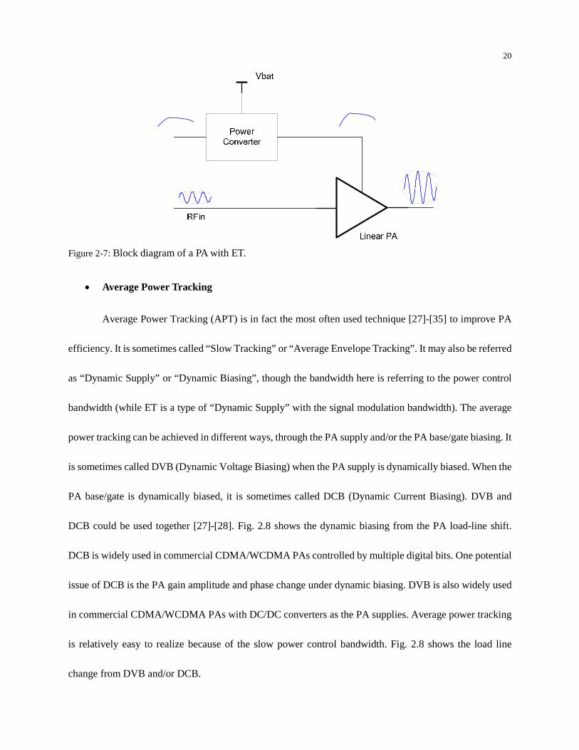
Figure 2-7: Block diagram of a PA with ET.
• Average Power Tracking
Average Power Tracking (APT) is in fact the most often used technique [27]-[35] to improve PA
efficiency. It is sometimes called “Slow Tracking” or “Average Envelope Tracking”. It may also be referred
as “Dynamic Supply” or “Dynamic Biasing”, though the bandwidth here is referring to the power control
bandwidth (while ET is a type of “Dynamic Supply” with the signal modulation bandwidth). The average
power tracking can be achieved in different ways, through the PA supply and/or the PA base/gate biasing. It
is sometimes called DVB (Dynamic Voltage Biasing) when the PA supply is dynamically biased. When the
PA base/gate is dynamically biased, it is sometimes called DCB (Dynamic Current Biasing). DVB and
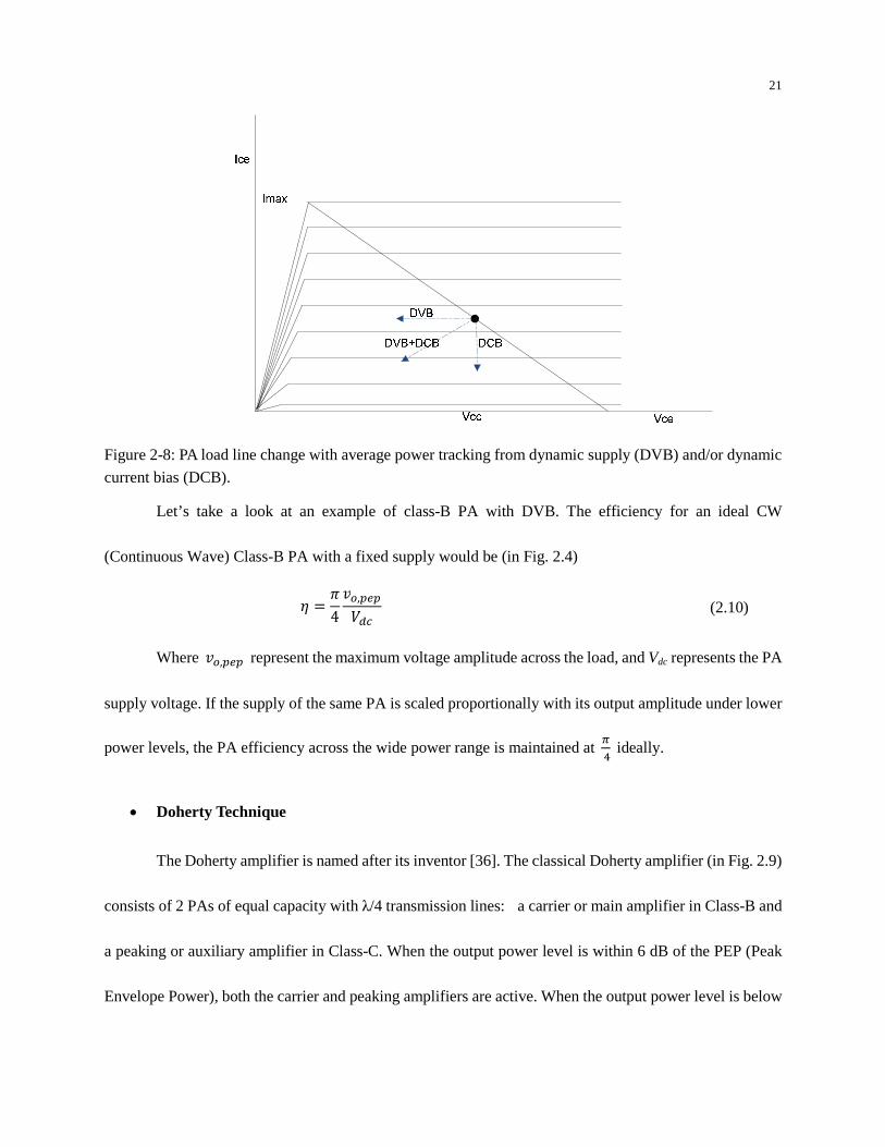
DCB could be used together [27]-[28]. Fig. 2.8 shows the dynamic biasing from the PA load-line shift.
DCB is widely used in commercial CDMA/WCDMA PAs controlled by multiple digital bits. One potential
issue of DCB is the PA gain amplitude and phase change under dynamic biasing. DVB is also widely used
in commercial CDMA/WCDMA PAs with DC/DC converters as the PA supplies. Average power tracking
is relatively easy to realize because of the slow power control bandwidth. Fig. 2.8 shows the load line
change from DVB and/or DCB.
21
Figure 2-8: PA load line change with average power tracking from dynamic supply (DVB) and/or dynamic
current bias (DCB).
Let’s take a look at an example of class-B PA with DVB. The efficiency for an ideal CW
(Continuous Wave) Class-B PA with a fixed supply would be (in Fig. 2.4)
+4 ,;-;(< (2.10)
Where ,;-; represent the maximum voltage amplitude across the load, and Vdc represents the PA
supply voltage. If the supply of the same PA is scaled proportionally with its output amplitude under lower
power levels, the PA efficiency across the wide power range is maintained at = ? ideally.
• Doherty Technique
The Doherty amplifier is named after its inventor [36]. The classical Doherty amplifier (in Fig. 2.9)
consists of 2 PAs of equal capacity with λ/4 transmission lines: a carrier or main amplifier in Class-B and
a peaking or auxiliary amplifier in Class-C. When the output power level is within 6 dB of the PEP (Peak
Envelope Power), both the carrier and peaking amplifiers are active. When the output power level is below
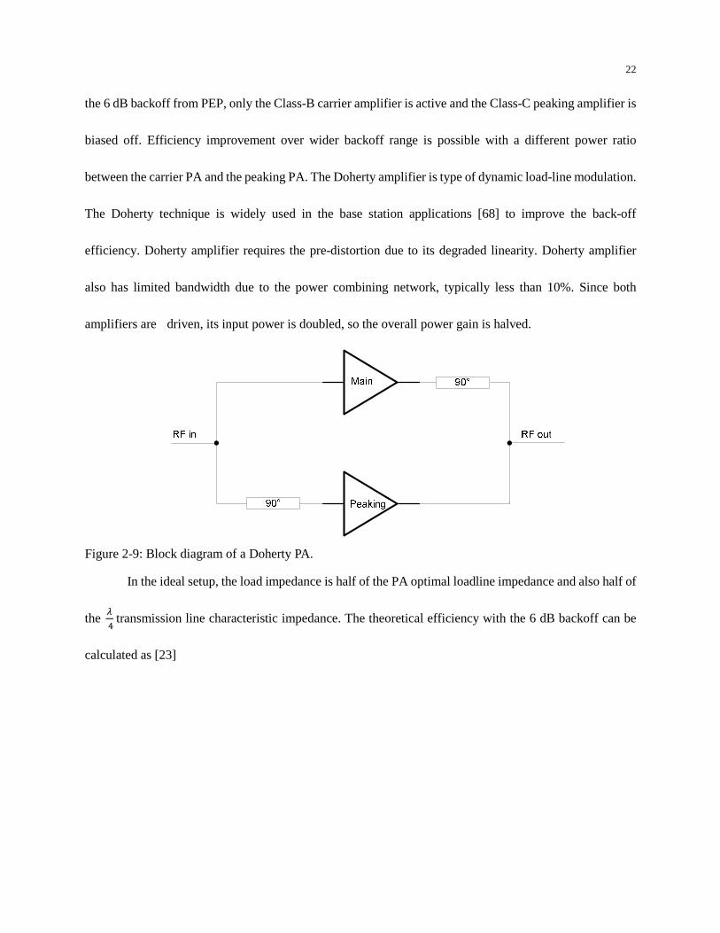
22
the 6 dB backoff from PEP, only the Class-B carrier amplifier is active and the Class-C peaking amplifier is
biased off. Efficiency improvement over wider backoff range is possible with a different power ratio
between the carrier PA and the peaking PA. The Doherty amplifier is type of dynamic load-line modulation.
The Doherty technique is widely used in the base station applications [68] to improve the back-off
efficiency. Doherty amplifier requires the pre-distortion due to its degraded linearity. Doherty amplifier
also has limited bandwidth due to the power combining network, typically less than 10%. Since both
amplifiers are driven, its input power is doubled, so the overall power gain is halved.
Figure 2-9: Block diagram of a Doherty PA.
In the ideal setup, the load impedance is half of the PA optimal loadline impedance and also half of
the @ ? transmission line characteristic impedance. The theoretical efficiency with the 6 dB backoff can be
calculated as [23]
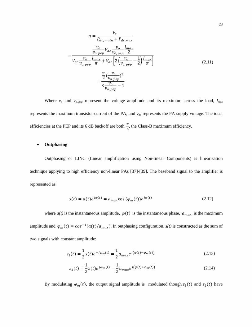
23
<, <,
, ;-; (< , ;-; )2(< , ;-; )+ (< A2 B , ;-; 12C )+ D
+2 , ;-;,3 , ;-; 1
(2.11)
Where vo and vo, pep represent the voltage amplitude and its maximum across the load, Imax
represents the maximum transistor current of the PA, and vdc represents the PA supply voltage. The ideal
efficiencies at the PEP and its 6 dB backoff are both = ?, the Class-B maximum efficiency.
• Outphasing
Outphasing or LINC (Linear amplification using Non-linear Components) is linearization
technique applying to high efficiency non-linear PAs [37]-[39]. The baseband signal to the amplifier is
represented as
E. F.GHI Fcos J.GHI (2.12)
where a(t) is the instantaneous amplitude, J. is the instantaneous phase, F is the maximum
amplitude and J. KELMF./F. In outphasing configuration, s(t) is constructed as the sum of
two signals with constant amplitude:
EM. 12 E.GLHIO 12 FGHPILIOQ (2.13)
E,. 12 E.GHIO 12 FGHPIRIOQ (2.14)
By modulating J., the output signal amplitude is modulated though EM. and E,. have
24
constant amplitude. High efficiency non-linear amplifiers can be used for both amplifiers. DSP at baseband
is used to calculate the required J. at any given time for the particular signal amplitude.
Raab [37] shows that a simple outphasing consists of 2 Class-B PAs would not gain any backoff
efficiency improvement. The Chireix technique uses the shunt reactances to tune out the PA load reactances
to optimize the efficiency at a particular output signal amplitude. Assuming the two outphasing PAs are
Class-B type, the efficiency can be calculated [37] from the outphasing configuration in Fig. 2.10.
Figure 2-10: Block diagram of a out-phasing PA.
< +4 B , ;-;C,
STB , ;-;C, U V , ;-; W1 B , ;-;C, XY2X Z9[ST
=
\]]_
=? `a`a, bcb , if Z9 0 =? , if Z9 ,fafg `a`a, bcb W1 h `a`a, bcbi, T
(2.15)
As we can see, the backoff efficiency is the same as the Class-B PA if Z9 set to 0. However, the
25
backoff efficiency at a particular output amplitude vo would be maintained at =? if Z9 is set to
,fafg `a`a, bcb W1 h `a`a, bcbi,. At other output amplitudes, the efficiency would be lower than
= ?. The overall
efficiency for a particular signal profile can be maximized by the proper selection of the shunt reactance
with the consideration of the signal PDF (Probability Density Function). Effectively the output power and
linearity control is achieved by the PA load impedance modulation.
Fig. 2.11 from [40] representatively shows the efficiency improvement of these different
techniques compared against a Class-A or Class-B amplifier. These techniques could potentially be
combined together for further improvement. There are more discussions on the topic for the high PAR
wideband systems in Section 3.3 of next chapter.
Figure 2-11: Representative PA efficiency vs its output envelop for different techniques [40].
26
2.1.5 Linearity Enhancement Techniques
Often times high efficiency PA schemes need additional techniques to improve its linearity. These
may include feedback or feed-forward types. Open loop pre-distortion techniques are widely used to
compensate the PA nonlinear AM-AM and AM-PM responses. DPD (Digital Pre-Distortion) are realized in
the baseband by a DSP (Digital Signal Processing) processor. Fig. 2.12 shows a block diagram of adaptive
DPD. Pre-distortion could also be realized in the RF domain [41]. In the adaptive DPD systems, the
feedback loop is usually slow mainly for the correction of temperature and power levels, but too slow to
correct the signal tracking error. Fig. 2.12 shows a typical system level block diagram for an ET transmitter.
The baseband digital processor includes CFR (Crest Factor Reduction) and DPD.
Figure 2-12: Block diagram of a typical transmitter configuration with DPD.
Closed-loop feedbacks may also be used to correct the PA non-linearity, however it is usually
challenging to track the wideband modulated signal without the stability issue under various conditions,
particularly for the wideband modulation schemes. Fig. 2.13 shows the polar loop modulation, where the
27
EDGE power level and signal modulation is controlled through its feedback loop [2].
Figure 2-13: Block diagram of a typical polar transmitter configuration with closed-loop feedback.
2.2 Inductor-based Switching Mode Power Supplies
In general switching power supplies have the property of high efficiency, when compared with the
linear supplies. The conduction loss can be low with low Rdson switches. In the linear supplies, the power
devices may have to sustain large voltage while delivering the output current, and thus high conduction loss.
The boost converters can also generate higher output than its input, which is impossible with a linear supply.
The bandwidth of the switching mode power supplies is often limited by factors such as the switching
frequency, switching noise and power stage passive components.
2.2.1 Buck, Boost and Buck/Boost Switching Converters
There are 3 basic types of switching converters depending on the relationship of the output and its
input. Fig. 2.14 shows their configurations.
28
(a)
(b)
(c)
Figure 2-14: DC/DC switching converters. (a) buck, (b) boost, (c) buck/boost.
When the converters are configured in PWM (Pulse Width Modulation) with CCM (Continuous
Conduction Mode), their input and output relationships with respect to their duty cycles (ignoring the losses)
are shown in Table 2.1.
When the converters are configured in PWM with DCM (Discontinuous Conduction Mode), their
inductor currents are intended not to become negative to reduce the conduction losses. Their inputs and
29
outputs relationships with respect to their duty cycles (ignoring the losses) are shown in Table 2.1 as well
[42].
Table 2.1: DC/DC converter conversion ratio
Converter CCM M(D) DCM M(D,K)
Buck D 21 j1 4k/l,
Boost 1l 1 j1 4l,/k2
Buck-boost l1 l l√k
with K = 2L / RTs
2.2.2 Voltage Mode and Current Mode Controlled Switching Converters
Feedback is often utilized to ensure that good output regulation is maintained under various
conditions, such as input, load, temperature and process variations. There are two common methods for the
PWM loop control: the voltage mode and the current mode, shown in Fig. 2.15 and Fig. 2.16, respectively.
In the voltage mode, the control voltage is compared with a PWM ramp. In the current mode, the control
current is compared against the sensed inductor current. When the switching converters are configured in
the PWM mode, the switching effect can be linearized using average modeling [42], so linear modeling and
control techniques can be applied in the small-signal sense.
30
Figure 2-15: Block diagram of a buck converter with voltage mode control.
Figure 2-16: Block diagram of a buck converter with current mode control.
The control-to-output transfer functions for buck converters for the voltage mode control and
current mode control are given in Table 2.2 [42]:
31
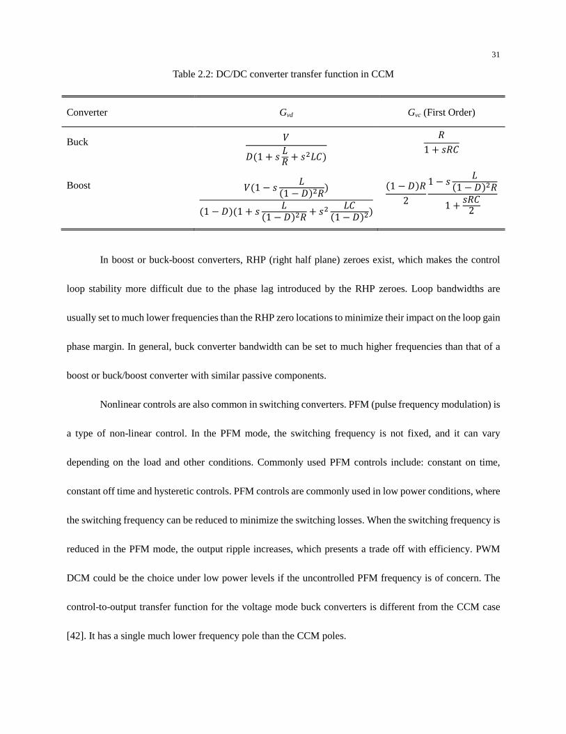
Table 2.2: DC/DC converter transfer function in CCM
Converter Gvd Gvc (First Order)
Buck (l1 E nX E,n8 X1 EX8
Boost (1 E n1 l,X1 l1 E n1 l,X E, n81 l,
1 lX2 1 E n1 l,X1 EX82
In boost or buck-boost converters, RHP (right half plane) zeroes exist, which makes the control
loop stability more difficult due to the phase lag introduced by the RHP zeroes. Loop bandwidths are
usually set to much lower frequencies than the RHP zero locations to minimize their impact on the loop gain
phase margin. In general, buck converter bandwidth can be set to much higher frequencies than that of a
boost or buck/boost converter with similar passive components.
Nonlinear controls are also common in switching converters. PFM (pulse frequency modulation) is
a type of non-linear control. In the PFM mode, the switching frequency is not fixed, and it can vary
depending on the load and other conditions. Commonly used PFM controls include: constant on time,
constant off time and hysteretic controls. PFM controls are commonly used in low power conditions, where
the switching frequency can be reduced to minimize the switching losses. When the switching frequency is
reduced in the PFM mode, the output ripple increases, which presents a trade off with efficiency. PWM
DCM could be the choice under low power levels if the uncontrolled PFM frequency is of concern. The
control-to-output transfer function for the voltage mode buck converters is different from the CCM case
[42]. It has a single much lower frequency pole than the CCM poles.

32
Table 2.3: DC/DC converter transfer function in DCM
2.2.3 Power Converter Efficiency and Losses
Efficiency is often the most critical parameter in the switching converter design. Efficiency is
calculated as follows:
9: o99, o (2.16)
The losses include the conduction losses due to the switch resistance, the inductor DC and AC
resistance, the diode conduction loss, the quiescent current consumption, various switching losses, and the
output capacitor ESR conduction loss. The losses in a synchronous buck converter can be calculated as
o99, o < `-po; <p` <<- q-9- rsf
)Y,X<9,t X<9,u XY ()YΔ.wxyz|~9 12 8-(,~9 (<<-)YΔ.y|~9 )q( Y,X
(2.17)
The switch output capacitance related energy cycling is also often considered additional switching
loss term. However, careful investigation suggests that this loss can be represented by the voltage and
current overlap loss [43].
Converter Gvd (First Order)
Buck 2(l 1 2 11 E 1 2 X8
Boost 2(l 12 1 11 E 12 1 X8
33
2.3 Switching Noise and Spread Spectrum Analysis
Switching noise from the switching converters is a major concern, particularly regarding the
GSM/EDGE receiver band noise requirement (-67 dBm at 10 MHz and -79 dBm at 20 MHz).
2.3.1 Buck Converter Switching Noise
The buck converter generated switching noise amplitude (with the output capacitor ESR ignored) in
the frequency domain can be calculated by the Fourier series of the PWM pulse followed by the 2nd order
LC filter.
,~ ~9 ( 2+ sinl + S 11 U2+~9 nX 2+~9,n8S ( 12+n8~9, sinl +
(2.18)
sω is the switching radian frequency.
ESR contribution to the output switching noise from the inductor current ripple can be calculated
from the Fourier series of a triangle waveform.
,rsf~ ~9 ( 1+, Xn~9sinl +, (2.19)
The total switching noise would be
,, ,rsf, (2.20)
The low frequency output noise is often dominated by the capacitance term with low ESR value.
However the high frequency noise from ESR contribution will become dominant once the harmonic order is
high enough.

34
p 12+X · 8~9 (2.21)
If the duty cycle is D = 0.5, only the odd harmonics appears, otherwise it has both even and odd
harmonics and they are duty cycle dependent. The above equation indicates the higher order, the less
harmonic at the fixed frequency with the same peak-peak ripple conditions. For example, the switching
noise around 10 MHz for a fs = 1 MHz with L = 1 µH and C = 1 µF is ~1/10th of the noise for a fs = 10 MHz
with L = 0.1 µH and C = 0.1 µF, though the peak-peak ripple is about the same.
2.3.2 Boost Converter Switching Noise
The boost converter switching noise in the frequency domain can be calculated from the Fourier
series of the triangular output waveform.
,~ ~9 ( 1+,1 l,X8~9sin1 l +, (2.22)
ESR contribution to the boost switching noise can be calculated from the Fourier series of a
rectangular wave.
,rsf~ ~9 ( 2X+X sin1 l + (2.23)
The total switching noise would follow (4.5) like in the buck case.
Like the buck case, the low frequency output noise is often dominated by the capacitance term with
low ESR value. However the high frequency noise from ESR contribution will become dominant once the
harmonic order is high enough.
p 12+X · 8~91 l, (2.24)
It is clear that the boost converter noise is worse than buck (proportional to 1/n2 instead of 1/n3 in

35
the buck case). This is because only the output capacitor is a filter element while both the output capacitor
and inductor are filter elements in the buck case. Numerical values of the switching harmonics can be
simulated as well from the periodical steady state analysis of the switching converter [88].
To illustrate the relative numerical values and trends, the noise contributions from capacitance and
ESR are plotted for both buck and boost in Fig. 2.17. In this example, it is assumed that D = 0.9 for buck and
D = 0.1 for boost with Vin = 3.6 V, L = 1 µH, C = 4.7 µF, fs = 2 MHz, ESR = 10 mΩ, and load R = 5 Ω. The
results show the ESR contribution dominates at high frequency for both buck and boost, and that the boost
noise is much higher than the buck case. The boost noise has the trend of 1/n, -20 dB/decade, while the buck
noise has the trend of 1/n2, -40 dB/decade.
36
Figure 2-17: Buck and boost switching noise at different switching harmonics from ESR and capacitance
contributions.
2.3.3 Noise Reduction using Switching Frequency Dithering
Spread spectrum or switching frequency dithering is often used to spread the energy of the
switching harmonics peaks across wide bandwidth. This can be done by frequency-modulating (FM) the
switching converter clock signal. The spread spectrum amplitude can be analyzed (with 0 as the
switching radian frequency, 0 as the FM radian frequency and 0 as the switching radian frequency
deviation) [44]:
cos09. 0 cos0.. cos09. 00 sin0. (2.25)
100
101
102
-200
-150
-100
-50
Harmonic order n
Oup
ut n
oise
(dB
V)
boost ESR
boost C
buck ESRbuck C
1/n
1/n2
1/n3

37
cos09. B00CL cos09 0.
cos09. B00CMR/O7LMRAOD
cos09 0.
O is the FM modulation index. Jn is the n-th order Bessel function. The amplitude of each
mixing harmonic can simply be evaluated by the value of the Bessel function, which can be easily obtained
from Matlab or similar programs. The last approximation in (2.25) is from the Carson’s rule [45] to
approximate the FM bandwidth. The above equation is assuming the FM is produced from a sinusoidal
signal modulation. In practice, for easier realization,the modulation is oftendone using a triangular signal
modulation. The similar analysis can be done by first applying the Fourier series on the triangular wave.
cos09. 0 ~..
cos09. 0 8+, cos 0.M,,… .
cos09. 008+, 1n sin0.
M,,…
cos09.
L
L B 8+, 00CL B 827+, 00C cos09 0.
(2.26)
The last approximation of the above equation is ignoring the 3rd order above of the Fourier series.
When the high orders are considered, a lot of terms will appear. Fortunately the Bessel function is very
small for the higher Fourier orders of the triangle wave. Exact comparison of different modulation waves
can be simulated numerically from circuit simulators.
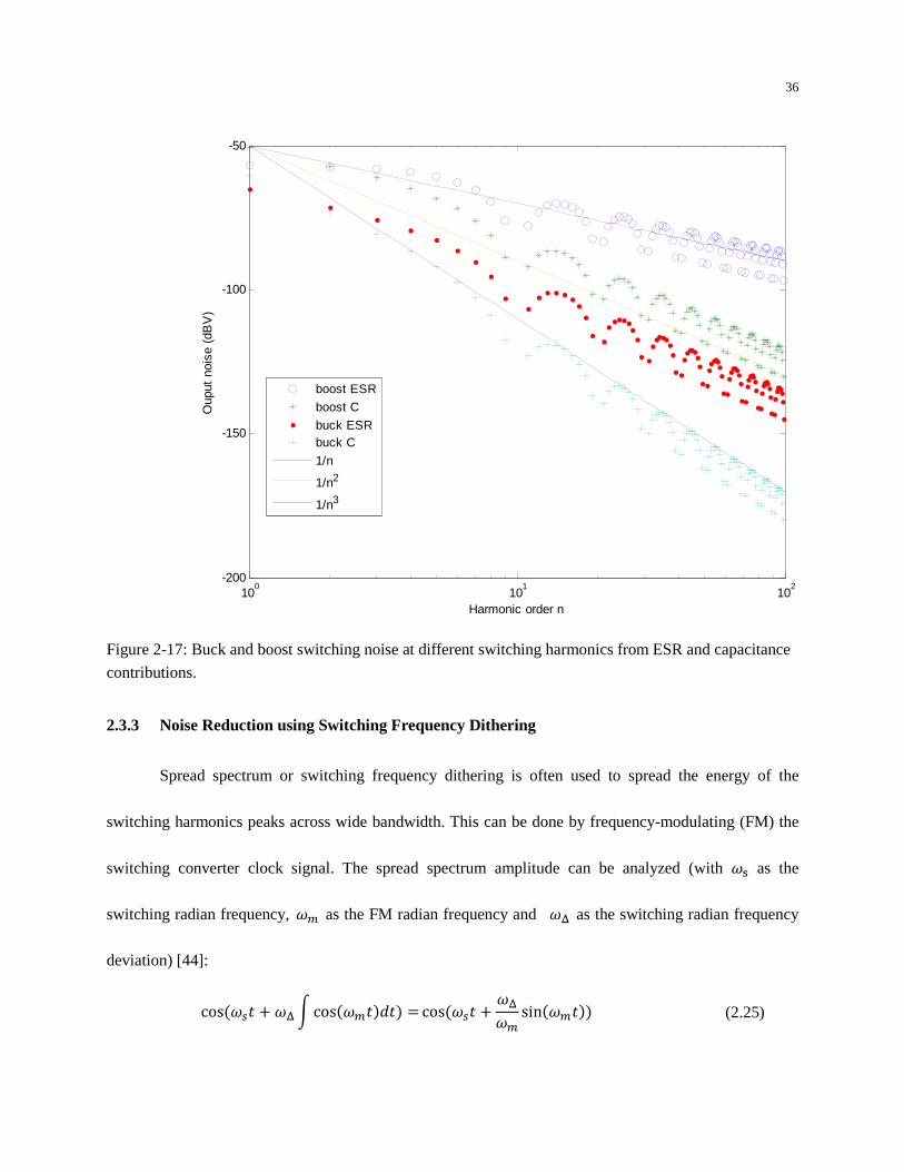
The peak noise reduction from the spread spectrum can be measured using a spectrum analyzer,

38
and the resolution bandwidth (RBW) of the analyzer has impact on the reduction magnitude [46]-[47]. We
can estimate the noise reduction by adding all the FM harmonic power inside the RBW. For example shown
in Fig. 2.18, assume the switching frequency fs = 200 kHz, FM deviation f∆ = ±20 kHz, and the sinusoidal
FM frequency fm = 1 kHz. The peak noise reduction with RBW = 9 kHz would be
1∑ f,OLf,O
~~ 1∑ ?L? 20 8.5 Z (2.27)
The reduction is insignificant when RBW ≥ f∆ because the total power of all the harmonics inside
this RBW is about the un-modulated total power (Carson’s rule). The reduction would be significant if
RBW << f∆. For example, if RBW = 200 Hz, the ideal peak reduction would be 1/20 15.5 dB. The
results can be verified from the transient simulations and then by Fourier transformer with different bin size
(RBW).
39
Figure 2-18: Switching noise reduction from switching frequency modulation with respective to RSW.
Intuitively, the noise reduction relationship to f∆, fm and RSW can be understood as the following.
Bigger f∆ can help the spectrum to spread into wider frequency range. Smaller fm can help the spectrum
spread into smaller resolution. Smaller RSW will enable the observer to see the smaller measurement bin
size. If RSW > fm , the total energy from multiple harmonics inside RSW needs integrated, and thus limits the
noise reduction. When the higher switching harmonic noise is considered, such as at GSM/EDGE receiver
band, frequency f∆ and fm should be scaled along with the fs harmonic order, which could result in the
spectrum overlapping from the spread adjacent orders. In this case, excessively high f∆ would not increase
the peak noise reduction.
-30 -20 -10 0 10 20 30-40
-35
-30
-25
-20
-15
-10
-5
0
Offset frequency (kHz)
Out
put
switc
hing
noi
se r
educ
tion
(dB
V)
RSW = 200 Hz
RSW = 9 kHz

40
Chapter 3
Power Supply Architectures for RF Power Amplifiers
The efficiency enhancement techniques for RF PAs have been reviewed briefly in Chapter 2. The
PA supply architectures for power tracking, envelope tracking and EER techniques are discussed in detail
in this chapter. The different architectures are compared. Choice of the supply architecture is often related
to the system requirements. A special section is devoted for the high PAR wideband systems such as LTE
and WiMAX. Another section briefly discusses the architectures for the high power applications.
3.1 Efficient Power Supply Architectures for RF PAs
The simplest architecture for PA average power tracking is the buck converter. For ET and EER
applications, buck converter bandwidth is often times not enough unless extreme switching frequency is
used ([48], [98]) where the switching losses are difficult to handle.
3.1.1 Buck and Buck/Boost for Average Power Tracking
Buck converters have been used widely in PA average power control for the 3G applications. PAs
are linear in this architecture. Buck in these applications needs to have fast transient response for power
level transitions. The output capacitor cannot be too large, often in the µF range.
As the battery voltage drops lower when it discharges to lower capacity, PA supplied by the buck
41
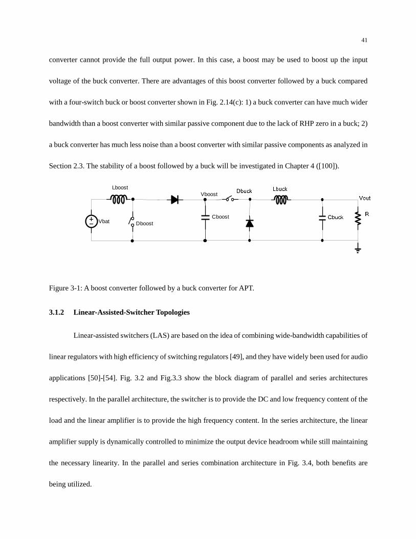
converter cannot provide the full output power. In this case, a boost may be used to boost up the input
voltage of the buck converter. There are advantages of this boost converter followed by a buck compared
with a four-switch buck or boost converter shown in Fig. 2.14(c): 1) a buck converter can have much wider
bandwidth than a boost converter with similar passive component due to the lack of RHP zero in a buck; 2)
a buck converter has much less noise than a boost converter with similar passive components as analyzed in
Section 2.3. The stability of a boost followed by a buck will be investigated in Chapter 4 ([100]).
Lboost
Cboost
Vboost
Vbat Dboost
Figure 3-1: A boost converter followed by a buck converter for APT.
3.1.2 Linear-Assisted-Switcher Topologies
Linear-assisted switchers (LAS) are based on the idea of combining wide-bandwidth capabilities of
linear regulators with high efficiency of switching regulators [49], and they have widely been used for audio
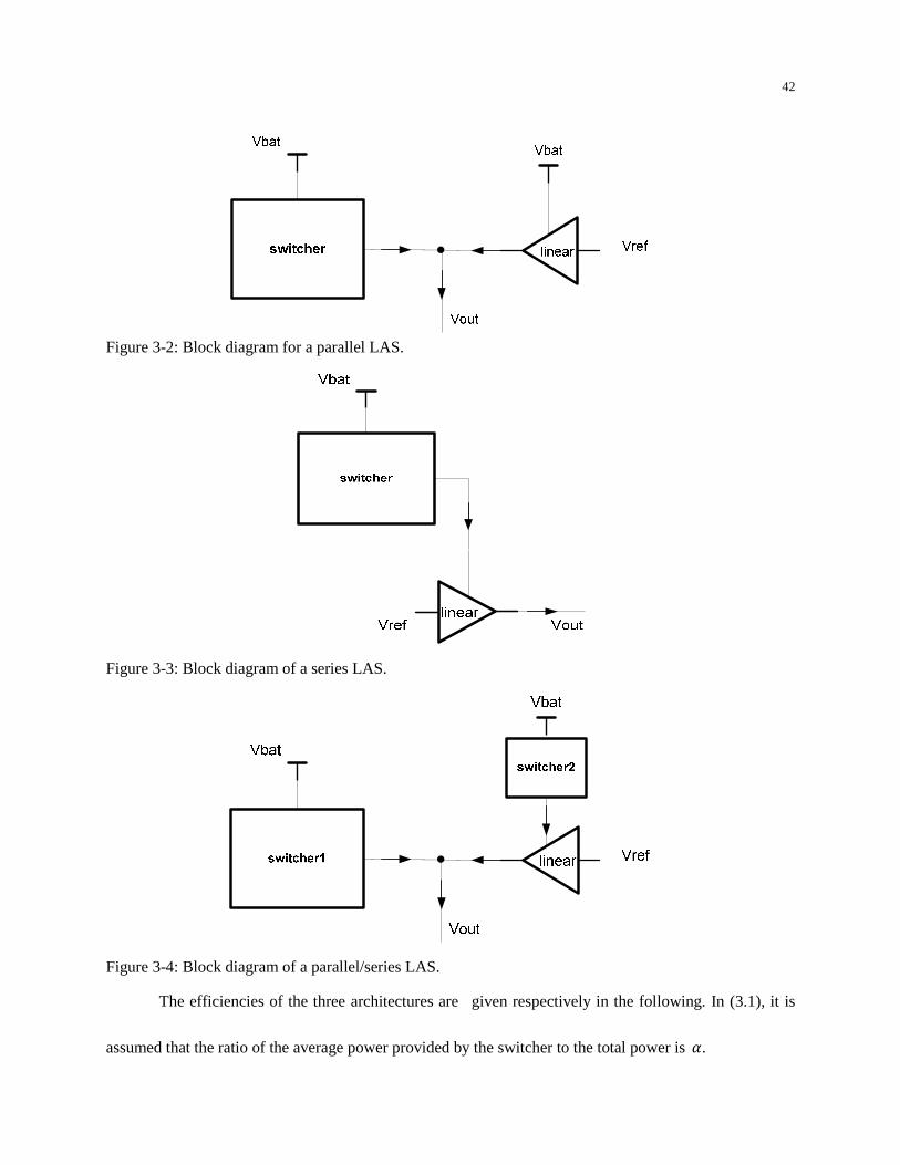
applications [50]-[54]. Fig. 3.2 and Fig.3.3 show the block diagram of parallel and series architectures
respectively. In the parallel architecture, the switcher is to provide the DC and low frequency content of the
load and the linear amplifier is to provide the high frequency content. In the series architecture, the linear
amplifier supply is dynamically controlled to minimize the output device headroom while still maintaining
the necessary linearity. In the parallel and series combination architecture in Fig. 3.4, both benefits are
being utilized.
42
Figure 3-2: Block diagram for a parallel LAS.
Figure 3-3: Block diagram of a series LAS.
Figure 3-4: Block diagram of a parallel/series LAS.
The efficiencies of the three architectures are given respectively in the following. In (3.1), it is
assumed that the ratio of the average power provided by the switcher to the total power is .
43
19: 1 o (3.1)
9:o (3.2)
19:M 1 9:,o (3.3)
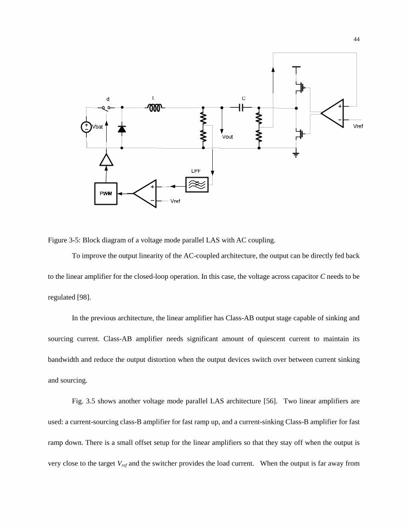
3.1.3 Voltage Mode Parallel LAS Architectures
A voltage mode parallel LAS architecture is shown in Fig. 3.5 (similar to [55]). This is sometimes
called split-band LAS, referring the high frequency of the output power is delivered by the linear amplifier
while the low frequency and DC content is delivered by the switcher. The low pass filter for the buck
reference is used to set the band-split frequency, i.e, low frequency power is delivered by the buck and high
frequency power is delivered by the linear amplifier. The corner frequency of the low pass filter need to be
lower than the buck control bandwidth, otherwise the buck control bandwidth will be the band-split
frequency. The current sharing between buck and linear amplifier is handled by the AC-coupling capacitor,
which is also effectively acting as the output filter capacitor for the buck. The switching ripple is filtered
by the wideband linear amplifier through the capacitor. There are potential issues with this architecture: 1)
High frequency output distortion as the output is not closed-loop controlled by the linear amplifier, and the
distortion is depending on the capacitance and load impedance; 2) Mid-band efficiency degradation as the
mid-band buck current (inside buck bandwidth) flows through the capacitor and absorbed by the linear
amplifier, and again this depends on the capacitance and load impedance.
44
Figure 3-5: Block diagram of a voltage mode parallel LAS with AC coupling.
To improve the output linearity of the AC-coupled architecture, the output can be directly fed back
to the linear amplifier for the closed-loop operation. In this case, the voltage across capacitor C needs to be
regulated [98].
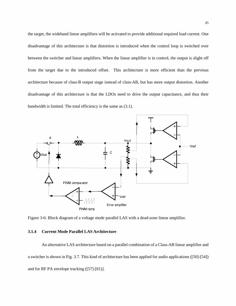
In the previous architecture, the linear amplifier has Class-AB output stage capable of sinking and
sourcing current. Class-AB amplifier needs significant amount of quiescent current to maintain its
bandwidth and reduce the output distortion when the output devices switch over between current sinking
and sourcing.
Fig. 3.5 shows another voltage mode parallel LAS architecture [56]. Two linear amplifiers are
used: a current-sourcing class-B amplifier for fast ramp up, and a current-sinking Class-B amplifier for fast
ramp down. There is a small offset setup for the linear amplifiers so that they stay off when the output is
very close to the target Vref and the switcher provides the load current. When the output is far away from
45
the target, the wideband linear amplifiers will be activated to provide additional required load current. One
disadvantage of this architecture is that distortion is introduced when the control loop is switched over
between the switcher and linear amplifiers. When the linear amplifier is in control, the output is slight off
from the target due to the introduced offset. This architecture is more efficient than the previous
architecture because of class-B output stage instead of class-AB, but has more output distortion. Another
disadvantage of this architecture is that the LDOs need to drive the output capacitance, and thus their
bandwidth is limited. The total efficiency is the same as (3.1).
Figure 3-6: Block diagram of a voltage mode parallel LAS with a dead-zone linear amplifier.
3.1.4 Current Mode Parallel LAS Architecture
An alternative LAS architecture based on a parallel combination of a Class-AB linear amplifier and
a switcher is shown in Fig. 3.7. This kind of architecture has been applied for audio applications ([50]-[54])
and for RF PA envelope tracking ([57]-[61)].
46
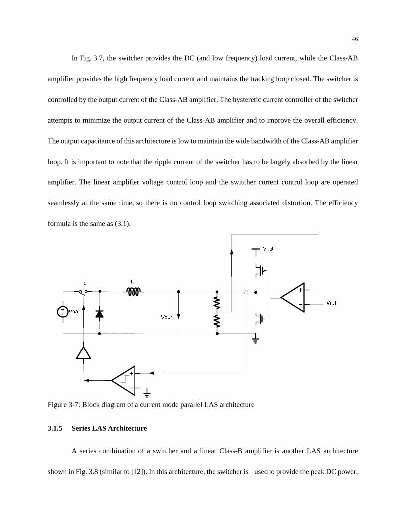
In Fig. 3.7, the switcher provides the DC (and low frequency) load current, while the Class-AB
amplifier provides the high frequency load current and maintains the tracking loop closed. The switcher is
controlled by the output current of the Class-AB amplifier. The hysteretic current controller of the switcher
attempts to minimize the output current of the Class-AB amplifier and to improve the overall efficiency.
The output capacitance of this architecture is low to maintain the wide bandwidth of the Class-AB amplifier
loop. It is important to note that the ripple current of the switcher has to be largely absorbed by the linear
amplifier. The linear amplifier voltage control loop and the switcher current control loop are operated
seamlessly at the same time, so there is no control loop switching associated distortion. The efficiency
formula is the same as (3.1).
Figure 3-7: Block diagram of a current mode parallel LAS architecture
3.1.5 Series LAS Architecture
A series combination of a switcher and a linear Class-B amplifier is another LAS architecture
shown in Fig. 3.8 (similar to [12]). In this architecture, the switcher is used to provide the peak DC power,
47
and the linear amplifier is to provide the modulation envelope or fast transient requirement like the
GSM/EDGE time mask. The total efficiency is shown in (3.2).
Figure 3-8: Block diagram of a series LAS architecture.
This architecture is efficient for the modulation with low PAR as the linear amplifier would be
efficient with its output not too far from its input. One advantage of this architecture over the parallel
architectures is that the switcher can have a relative large output capacitance to reduce its switching noise,
while at the same time the linear amplifier can have a low capacitance for higher bandwidth with low
quiescent current. Another advantage of this architecture is that the switcher can be a boost or buck/boost
converter instead of buck only in the parallel architectures.
48
3.2 Architecture Selection
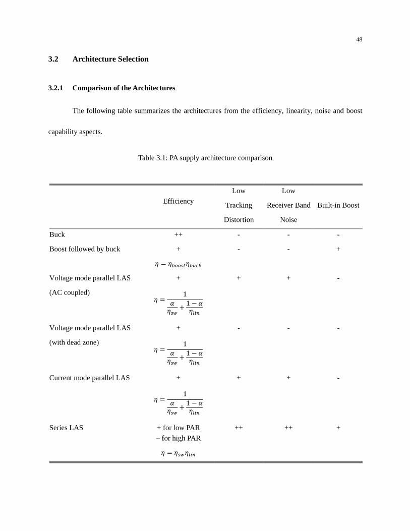
3.2.1 Comparison of the Architectures
The following table summarizes the architectures from the efficiency, linearity, noise and boost
capability aspects.
Table 3.1: PA supply architecture comparison
Efficiency
Low
Tracking
Distortion
Low
Receiver Band
Noise
Built-in Boost
Buck ++ - - -
Boost followed by buck + 9
- - +
Voltage mode parallel LAS
(AC coupled)
+
19: 1 o
+ +
-
Voltage mode parallel LAS
(with dead zone)
+
19: 1 o
- - -
Current mode parallel LAS
+
19: 1 o
+ + -
Series LAS + for low PAR
– for high PAR 9:o
++ ++ +

49
3.2.2 Architecture Choices for Different RF PA Modes
The architecture selection is a difficult task driven by the system requirements.
For the GSM/EDGE applications, the average power tracking may be used for the PA supply, while
the time mask requirement and modulation are handled by the PA RF input and/or base/gate bias. In these
applications, a buck converter or a boost followed by buck may be used.
For the polar GSM/EDGE applications, both the power and modulation are handled from the PA
supply, while PAs are in saturation with their input being over-driven. In these applications, wideband
supplies are required. Traditionally they are from LDOs with input tied to battery directly. While LDOs are
efficient for high power conditions, they are inefficient for low power conditions. A current-mode parallel
or series LAS architecture could be suitable for the polar EDGE applications.
For the WCDMA/HSPA applications, average power tracking is often used for the PA supply. A
series LAS architecture is not suitable as their PAR is much higher than that of the EDGE signal. A
current-mode parallel LAS architecture may be suitable for the high power conditions, however the
WCDMA average usage indicates the maximum PDF is located in the low power conditions (-2 dBm for
voice applications). The quiescent current of the Class-AB linear amplifier would be difficult for the
converter to achieve high efficiency under low power conditions. In the following, we will take a look at an
example.
The current mode parallel architecture is used in [10] with 50 MHz bandwidth reported, and the
good efficiency is mentioned for the high power levels. As we know, the efficiency for a low power level in
the WCDMA/HSPA systems is even more critical as the probability is highest around -2 dBm. We can see
50
the efficiency rapidly decreases from the DC/DC alone 77% down to the LAS modulator 46% even for a
relatively high output power level 24.3 dBm (Vout = 2 V and Iout = 135 mA). This is mainly due to the
quiescent current loss of the wideband Class-AB linear amplifier, estimated about 59 mA quiescent current
(translated to 0.3% @ -2 dBm output power).
3.2.3 Buck/Boost-LDO Series Architecture as Multi-Mode RF PA Supply
The buck/boost and Class-B linear amplifier (LDO) series architecture shown in Fig. 3.8 is
proposed as the multi-mode PA supply. This architecture is capable of GSM, linear EDGE, polar EDGE,
and linear WCDMA/HSPA operations. When it is configured in the GSM mode, the buck/boost provides
the average power control. The linear amplifier is in tracking mode for the time mask ramp up and down
requirements, but it is acting as a switch once the output settles to the steady state. The buck/boost reference
Vpeak represents the slow varying power control level, and the linear amplifier reference Vref represents the
GSM burst with the time mask requirement. By setting Vref steady state near Vpeak, the linear amplifier is in
the drop out mode during its steady state, so the overall high efficiency is achieved.
For the linear EDGE operation, the PA supply is working similarly as the GSM mode. In this case,
the EDGE modulation is achieved from the linear PA RF input. The linear WCDMA operation works
similarly (in APT mode).
For the polar EDGE operation, the PA is saturated with constant envelope input. The PA supply
Vcc contains the modulation envelope. In this case, the buck/boost delivers the peak power (in APT mode),
while the linear amplifier outputs the required modulation (in EER mode). Again the linear amplifier also
provides the time mask requirement. The reference Vpeak is set to the peak level of the linear amplifier
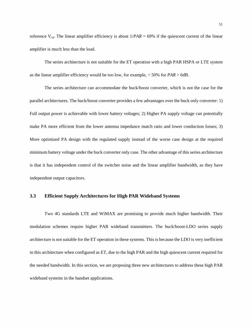
51
reference Vref. The linear amplifier efficiency is about 1/PAR = 69% if the quiescent current of the linear
amplifier is much less than the load.
The series architecture is not suitable for the ET operation with a high PAR HSPA or LTE system
as the linear amplifier efficiency would be too low, for example, < 50% for PAR > 6dB.
The series architecture can accommodate the buck/boost converter, which is not the case for the
parallel architectures. The buck/boost converter provides a few advantages over the buck only converter: 1)
Full output power is achievable with lower battery voltages; 2) Higher PA supply voltage can potentially
make PA more efficient from the lower antenna impedance match ratio and lower conduction losses; 3)
More optimized PA design with the regulated supply instead of the worse case design at the required
minimum battery voltage under the buck converter only case. The other advantage of this series architecture
is that it has independent control of the switcher noise and the linear amplifier bandwidth, as they have
independent output capacitors.
3.3 Efficient Supply Architectures for High PAR Wideband Systems
Two 4G standards LTE and WiMAX are promising to provide much higher bandwidth. Their
modulation schemes require higher PAR wideband transmitters. The buck/boost-LDO series supply
architecture is not suitable for the ET operation in these systems. This is because the LDO is very inefficient
in this architecture when configured as ET, due to the high PAR and the high quiescent current required for
the needed bandwidth. In this section, we are proposing three new architectures to address these high PAR
wideband systems in the handset applications.

52
3.3.1 Parallel/Series ET Architecture
One technique to improve the PA backoff efficiency is to adopt the ET technique, where the PA
supply is instantaneously adjusted to follow its modulation envelope to reduce the unnecessary supply
headroom during the backoff. The required bandwidth for the ET PA supply in LTE and WiMAX handsets
is in the range of 20 MHz, and the PAR is around 7dB.
Fig. 3.9 shows the proposed parallel/series ET architecture (similar to [62] and [101]). It is
fundamentally a current mode parallel LAS, with a buck-boost dynamically adjusting the wideband linear
amplifier supply. The current mode buck is to provide the DC power to the PA, while the wideband linear
amplifier is to provide the instantaneous AC power to the PA. Instead of using the Vbat as the supply for the
linear amplifier in the standard parallel architecture, a buck/boost is used instead (as APT for the linear
amplifier supply). There are a few advantages of adding the buck/boost to the architecture: 1) to deliver the
full power under the lower battery voltages; 2) to further improve the linear amplifier efficiency with the
slow dynamic supply (especially for low power levels); 3) to achieve higher PA supply for better PA
efficiency and optimization. In the practical configuration, the buck output at the peak levels could be
higher than Vbat by the linear amplifier feedback loop, however the average is still lower than Vbat due to the
high PAR.
53
Figure 3-9: Block diagram of parallel/series envelope tracking architecture.
The wideband linear amplifier is a Class-AB type, capable of both sinking and sourcing. It is very
challenging to meet the bandwidth requirement from a standard CMOS process and the quiescent current
would be prohibitively high if the bandwidth was achieved in this process. A high speed BJT or BiCMOS
process would be preferred for the linear amplifier efficiency concern. Darlington output devices are often
used for the high current and high speed purposes. On the other hand, emitter-follower Darlington structure
requires significant headroom (often in the range of 3 V) compared with the common emitter devices. One

54
way to further improve the linear amplifier efficiency is to have split supplies for the drivers of the output
devices. The driver supplies could be obtained from the DC/DC charging pumps as the required power is
limited for the drivers. This technique has been used for the DSL line driver applications [63]. Alternatively
common emitter output devices may be used, but it is more challenging to achieve the wide bandwidth
requirement.
When this architecture is implemented, it could be a single BiCMOS IC, or two-chip partition with
a high speed BJT process for the linear amplifier, and a standard CMOS process for the current mode buck,
and the buck/boost. Though the linear amplifier is required to provide the high peak current pulses, the
peak energy from the pulse is limited. The buck/boost switches could be much smaller than the buck
switches, as the output capacitor of the buck/boost would be the energy buffer for the linear amplifier high
current peaks.
While this architecture can potentially provide excellent efficiency for the PA peak and backoff
efficiency, there is still concern about the architecture efficiency in the low power conditions, as the linear
amplifier quiescent current is likely in the order of tens of mAs for the bandwidth and peak current
requirements.
3.3.2 Average Power Tracking Supply for Doherty PAs
Doherty architectures are often used to address the backoff efficiency issue. The architecture has
been used to address the high modulation PAR in the multi-carrier WCDMA base-station applications as
well [68]. The standard Doherty architecture consists of two parallel PAs biased differently: the carrier PA
(in Class-B or Class-AB) is alone to provide the output power up to 6 dB from its peak power, and the

55
peaking PA (in Class-C) is activated along with the carrier PA when the output power within 6 dB of its
peak power. The overall efficiency would be near 78.5% for the output power levels within 6 dB from the
peak.
In the handset applications, the power control range is very wide (such as 80 dB for WCDMA) and
the low power efficiency is often very important for the handset talk time. This is a significantly different
from the base station-applications, where the relatively constant output power is required due to the
overhead channels. In (2.11), the ideal Doherty efficiency is calculated based on the assumption that the PA
output peak envelope , ;-; is at its DC supply (<. If the system requests PA output in the low power
conditions, the Doherty PA efficiency would be its carrier class-B amplifier efficiency if the supply is fixed.
<, +4 (< (3.4)
However if the Doherty PA supply has the power tracking such that the PA output peak envelope
, ;-; is always at its DC supply ( even under the low power conditions, the ideal Doherty efficiency
in (2.11) would be maintained in the low power levels. Of course, the auxiliary amplifier bias has to be
adjusted properly in the low power levels to main the Doherty 6 dB backoff property. The advantage of the
Doherty property (on top of the power tracking) is to maintain the good efficiency over the wideband 6 dB
signal dynamic range (over the wide power control range). The advantage of this approach compared with
the ET approach in the previous section is that the power tracking supply for the PA would be a simple and
very efficient DC/DC supply with very narrow bandwidth, since the PA power control bandwidth is in the
kHz range.
Fig. 3.10 shows a proposed architecture to address LTE and WiMAX handsets by applying the

56
Doherty concept for the wide power control range. It attempts to maintain the Doherty backoff efficiency
improvement property under low power levels, by dynamically and continuously adjusting the Doherty PA
supplies (in APT) and biases. In this architecture, a high efficiency buck/boost could be used for the
Doherty PAs. The key to maintaining the Doherty 6 dB efficiency over the wide power range, is the bias
control for the peaking PA (and possibly the carrier PA as well), as it needs dynamically adjusted (biased
lower at lower output power). The bias control and the supply control could be coordinated from a single
power feedback control loop. In this configuration, the PA biases and the supplies handle the average power
control, while the PA RF input (with modulation) will dynamically bias the peaking PA (via open loop) so
that the 6 dB efficiency enhancement is maintained for that particular average power level. A look-up-table
(from characterization) inside the baseband DSP ([64]) or as part of the pre-distortion may be used to
provide the complicated mapping from the output power to the bias control levels.
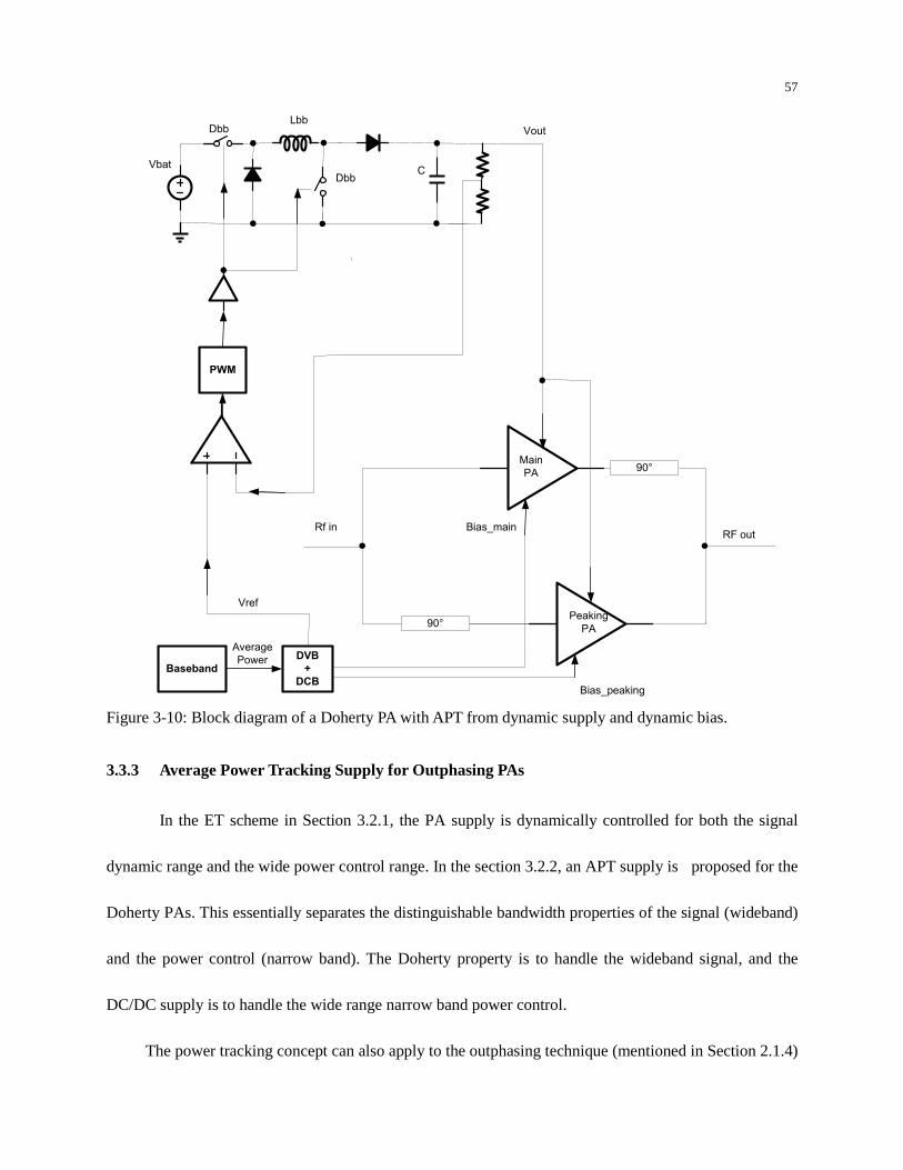
57
90°
90°
Rf inRF out
Main
PA
Peaking
PA
Vbat
PWM
Vout
Baseband
DVB
+
DCB
Bias_main
Bias_peaking
Average
Power
Lbb
CDbb
Dbb
Vref
Figure 3-10: Block diagram of a Doherty PA with APT from dynamic supply and dynamic bias.
3.3.3 Average Power Tracking Supply for Outphasing PAs
In the ET scheme in Section 3.2.1, the PA supply is dynamically controlled for both the signal
dynamic range and the wide power control range. In the section 3.2.2, an APT supply is proposed for the
Doherty PAs. This essentially separates the distinguishable bandwidth properties of the signal (wideband)
and the power control (narrow band). The Doherty property is to handle the wideband signal, and the
DC/DC supply is to handle the wide range narrow band power control.
The power tracking concept can also apply to the outphasing technique (mentioned in Section 2.1.4)
58
as well. In the outphasing technique, the PA has the constant envelope, and the PA linearity is achieved and
controlled through the load modulation by the phase angle between the outputs of the two PAs. In the low
power conditions with a fixed PA supply, the efficiency for the outphasing PAs would be much lower
than =?, as indicated in Fig. 2.11 as well. Under low power conditions, the efficiency can be approximated
from (2.15).
< +4 , ;-;,XY2X Z9 (3.5)
Since the shunt reactance is selected based on the average efficiency optimization over the signal
PDF, the efficiency at low power levels is quite low due to the highly reactive loads. For the high PAR
wideband application such as LTE and WiMAX, the outphasing linearization technique would be a good fit
for the wide bandwidth and higher PAR requirements. However the outphasing alone would be inefficient
for low power levels, as the shunt reactance can only be optimized for a particular power level. It would be
natural to apply the APT technique on the supplies of the outphasing PAs. By doing this, the Chireix
outphasing efficiency improvement property is essentially extended to the low power levels.
If the power control is applied on the supplies of the two outphasing PAs, the ideal efficiency
relationship would be maintained as the output PEP is scaled with the PA DC supply. Fig. 3.11 shows the
power tracking concept with a DC/DC as the supply. Similar concept is also mentioned for the outphasing
class-F PAs in the WLAN application [39]. In [7], ET on the outphasing Class-E PAs is discussed.
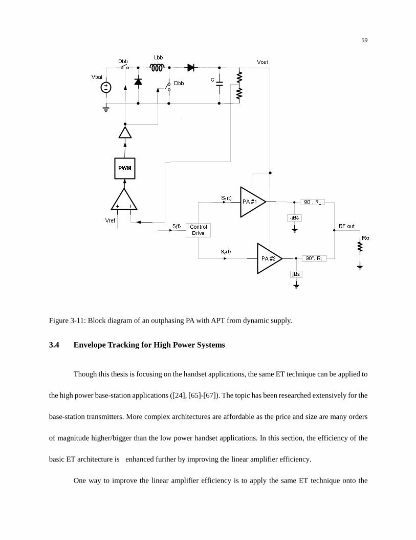
59
Figure 3-11: Block diagram of an outphasing PA with APT from dynamic supply.
3.4 Envelope Tracking for High Power Systems
Though this thesis is focusing on the handset applications, the same ET technique can be applied to
the high power base-station applications ([24], [65]-[67]). The topic has been researched extensively for the
base-station transmitters. More complex architectures are affordable as the price and size are many orders
of magnitude higher/bigger than the low power handset applications. In this section, the efficiency of the
basic ET architecture is enhanced further by improving the linear amplifier efficiency.
One way to improve the linear amplifier efficiency is to apply the same ET technique onto the

60
linear amplifier itself. In another word, it utilizes a more efficient wide-band switching buck to reduce the
load current requirement from the linear amplifier. This architecture becomes nested LAS architecture
shown in Fig. 3.12. This architecture is similar to [99], where more complicated DSP control is used
instead. Fig. 3.13 shows the simulated waveforms. As it can be seen, the linear amplifier output current has
very low amplitude ripple most of the time since the fast switcher will be able to deliver medium bandwidth
power to the output. Assuming the fast switcher is a lot more efficient than the linear amplifier, the overall
efficiency will be greatly improved.
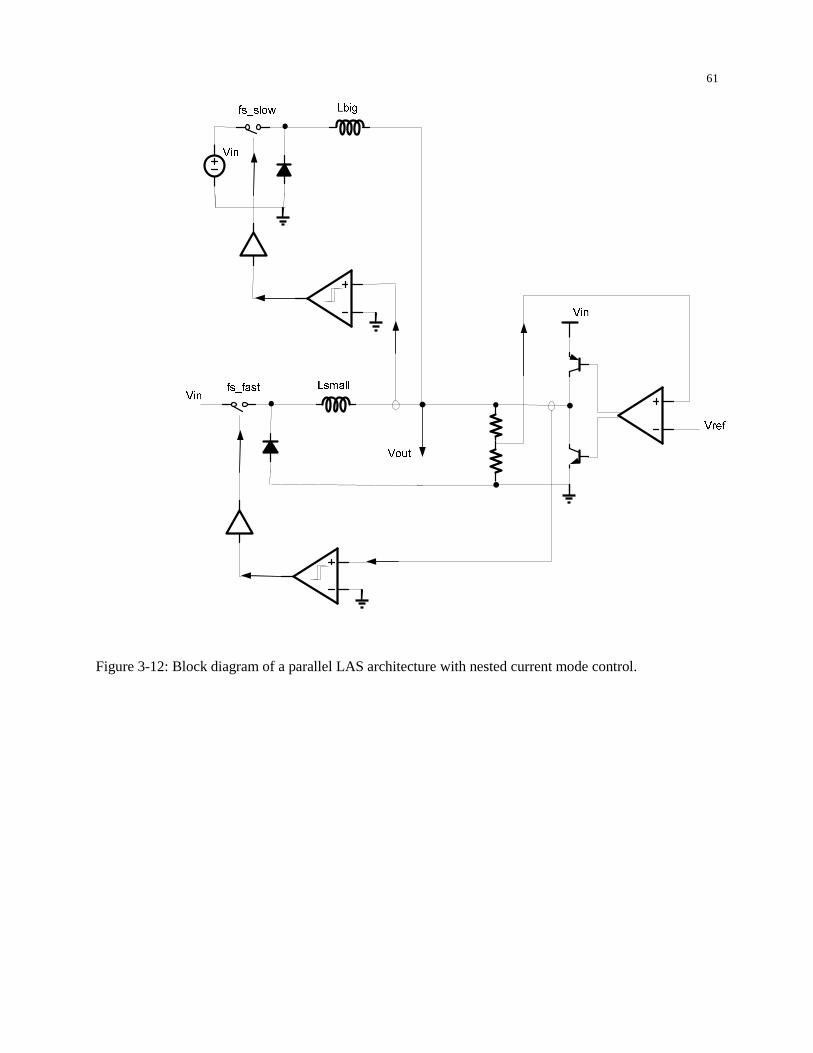
61
Figure 3-12: Block diagram of a parallel LAS architecture with nested current mode control.
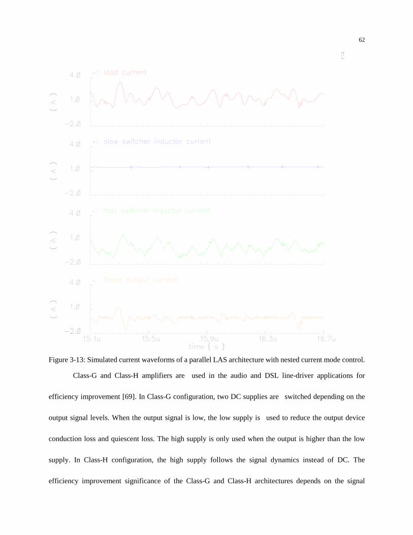
62
Figure 3-13: Simulated current waveforms of a parallel LAS architecture with nested current mode control.
Class-G and Class-H amplifiers are used in the audio and DSL line-driver applications for
efficiency improvement [69]. In Class-G configuration, two DC supplies are switched depending on the
output signal levels. When the output signal is low, the low supply is used to reduce the output device
conduction loss and quiescent loss. The high supply is only used when the output is higher than the low
supply. In Class-H configuration, the high supply follows the signal dynamics instead of DC. The
efficiency improvement significance of the Class-G and Class-H architectures depends on the signal
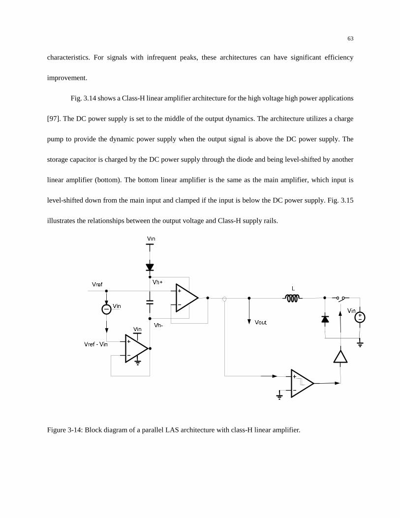
63
characteristics. For signals with infrequent peaks, these architectures can have significant efficiency
improvement.
Fig. 3.14 shows a Class-H linear amplifier architecture for the high voltage high power applications
[97]. The DC power supply is set to the middle of the output dynamics. The architecture utilizes a charge
pump to provide the dynamic power supply when the output signal is above the DC power supply. The
storage capacitor is charged by the DC power supply through the diode and being level-shifted by another
linear amplifier (bottom). The bottom linear amplifier is the same as the main amplifier, which input is
level-shifted down from the main input and clamped if the input is below the DC power supply. Fig. 3.15
illustrates the relationships between the output voltage and Class-H supply rails.
Figure 3-14: Block diagram of a parallel LAS architecture with class-H linear amplifier.
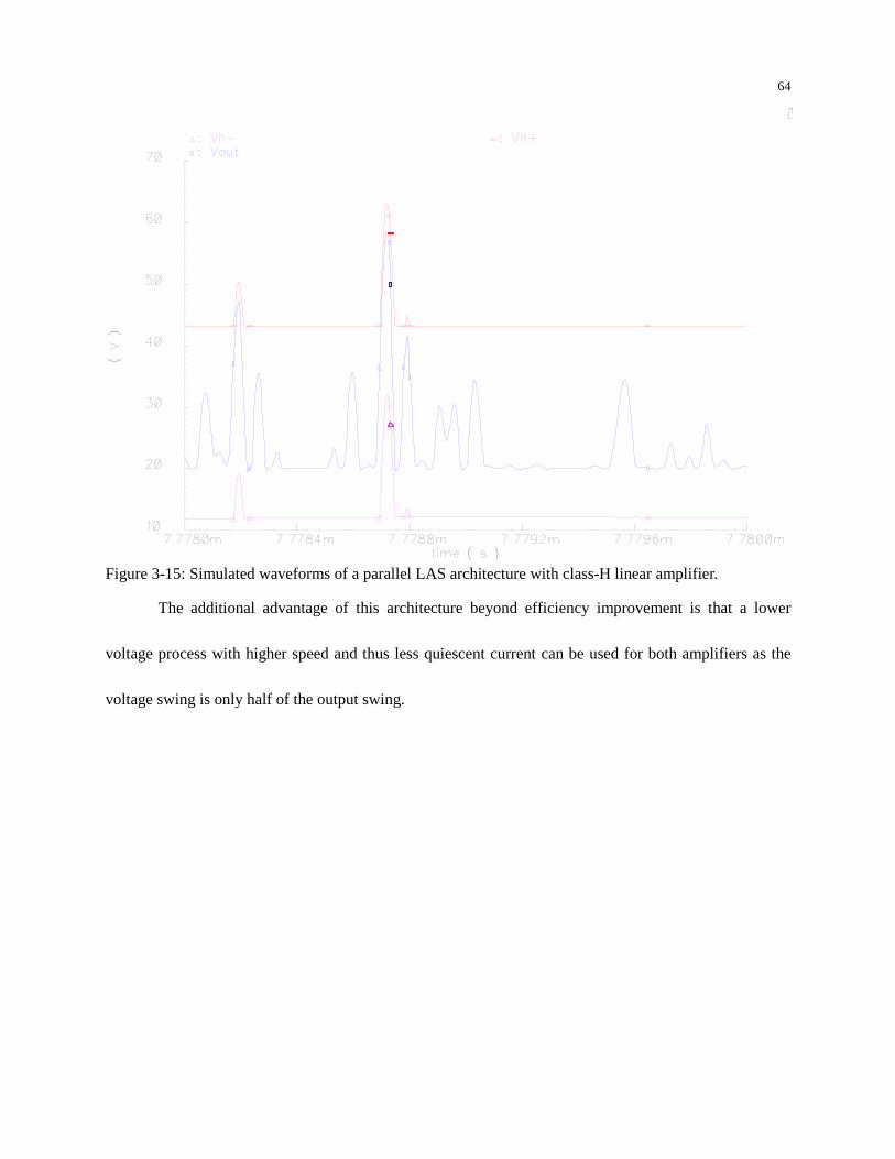
64
Figure 3-15: Simulated waveforms of a parallel LAS architecture with class-H linear amplifier.
The additional advantage of this architecture beyond efficiency improvement is that a lower
voltage process with higher speed and thus less quiescent current can be used for both amplifiers as the
voltage swing is only half of the output swing.
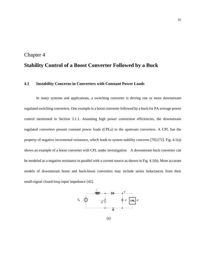
65
Chapter 4
Stability Control of a Boost Converter Followed by a Buck
4.1 Instability Concerns in Converters with Constant Power Loads
In many systems and applications, a switching converter is driving one or more downstream
regulated switching converters. One example is a boost converter followed by a buck for PA average power
control mentioned in Section 3.1.1. Assuming high power conversion efficiencies, the downstream
regulated converters present constant power loads (CPLs) to the upstream converters. A CPL has the
property of negative incremental resistance, which leads to system stability concerns [70]-[72]. Fig. 4.1(a)
shows an example of a boost converter with CPL under investigation. A downstream buck converter can
be modeled as a negative resistance in parallel with a current source as shown in Fig. 4.1(b). More accurate
models of downstream boost and buck-boost converters may include series inductances from their
small-signal closed-loop input impedance [42].
(a)
(
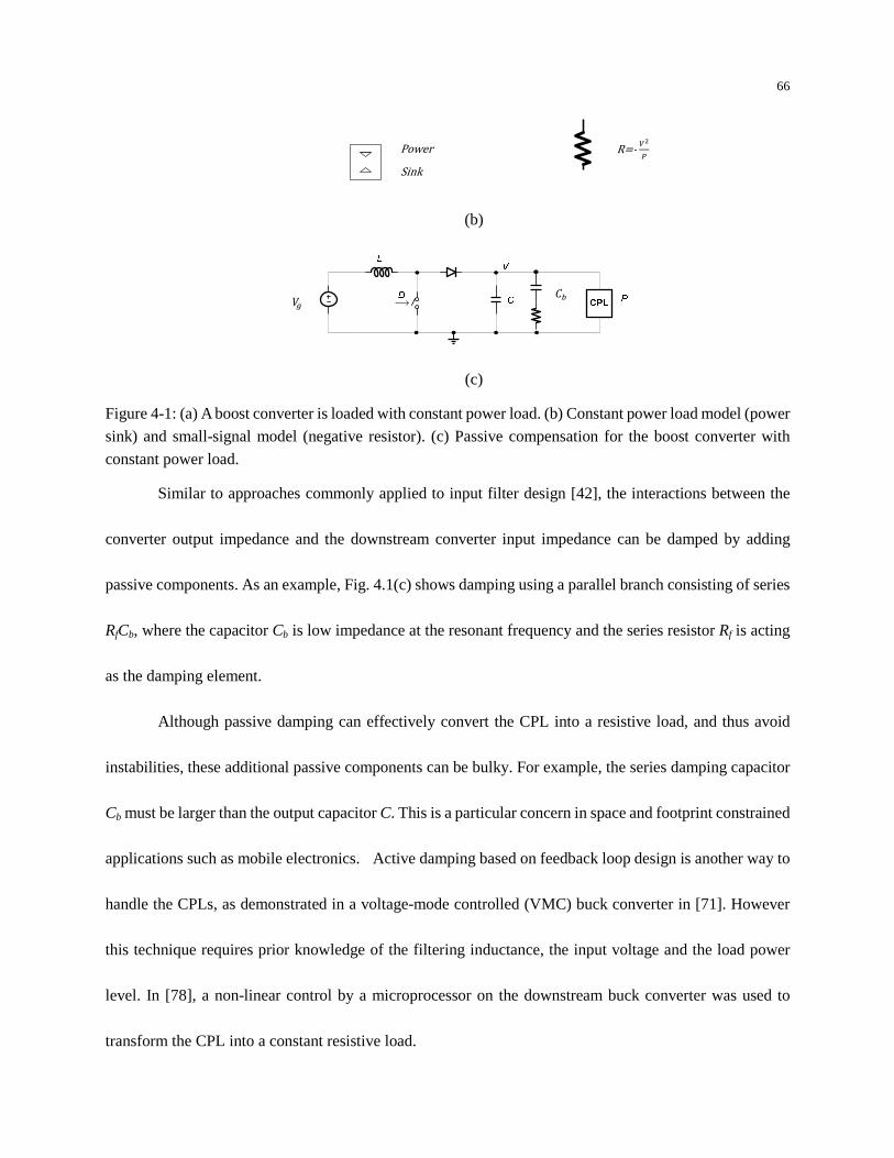
66
(b)
(c)
Figure 4-1: (a) A boost converter is loaded with constant power load. (b) Constant power load model (power
sink) and small-signal model (negative resistor). (c) Passive compensation for the boost converter with
constant power load.
Similar to approaches commonly applied to input filter design [42], the interactions between the
converter output impedance and the downstream converter input impedance can be damped by adding
passive components. As an example, Fig. 4.1(c) shows damping using a parallel branch consisting of series
RfCb, where the capacitor Cb is low impedance at the resonant frequency and the series resistor Rf is acting
as the damping element.
Although passive damping can effectively convert the CPL into a resistive load, and thus avoid
instabilities, these additional passive components can be bulky. For example, the series damping capacitor
Cb must be larger than the output capacitor C. This is a particular concern in space and footprint constrained
applications such as mobile electronics. Active damping based on feedback loop design is another way to
handle the CPLs, as demonstrated in a voltage-mode controlled (VMC) buck converter in [71]. However
this technique requires prior knowledge of the filtering inductance, the input voltage and the load power
level. In [78], a non-linear control by a microprocessor on the downstream buck converter was used to
transform the CPL into a constant resistive load.
R- t
8
X
(
Power Sink
67
The use of current-mode control (CMC) for the switching converters with CPLs has been
discussed in [79]-[81]. A CMC buck converter with CPL was investigated in [79] where it was shown that a
RHP pole and the related 180˚ phase shift exist in the control-to-output transfer function of the CPL current
control loop. In [80], the current control loop gain of a CMC full-bridge with CPL was investigated and the
Nyquist Criterion was used to determine stability of the system with RHP poles. In [81], the
control-to-output of the boost current control loop was approximated. This work pointed out that the
voltage loop control bandwidth cannot be set as in the resistive load case, which is a consequence of the low
frequency pole presented by the CPL current control loop.
The objectives of this chapter are to demonstrate the inherent active damping nature in the CMC
switching converters loaded by regulated downstream converters. The use of CMC is effectively
transforming the CPL into a resistive load, and consequently the conventional compensation scheme and
phase margin test can still be applied to the design of the CPL regulators. Peak current-mode control
(PCMC) modeling for boost converters with CPLs is discussed in Section 4.2. Section 4.3 addresses valley
current-mode control (VCMC) modeling for boost converters with CPLs.
Load current feedforward has been studied in the literature as a way to improve step load transients
for converters with resistive loads [82]-[84]. The feedforward technique has been discussed for a buck
converter with CPL in [85]. The effect of feedforward is modeled in Sections 4.2 and 4.3 for boost
converters with CPLs, using PCMC and VCMC, respectively. It is shown how the intended feedforward
becomes a feedback loop, which can potentially move the effective load pole between RHP and LHP (Left
Half Plane) depending on a feedforward coefficient.
Simulation results validating small-signal modeling and transient responses are presented in

68
Section 4.4. Section 4.5 summarizes this chapter.
4.2 Peak Current Mode Control for Boost converters with CPLs
A block diagram of a PCMC boost converter is shown in Fig. 4.2. The load current feedforward
path may or may not be present. The output capacitor series resistance (ESR) is not addressed in this paper
because low-ESR ceramic capacitors are often used in portable applications. From the CPL model in
Fig. 4.1(b), the VMC boost converter small-signal duty-to-output transfer function under CPL in
continuous-conduction-mode (CCM) can be found
`< (1 l 1 E n1 l, (,1 E n1 l, (, E, n81 l,
where P is the load power and V is output voltage.
(4.1)
Note that the transfer function has a RHP zero (as in the case of a resistive load), and a pair of RHP
poles due to the CPL incremental negative resistance. The objective in this and the next section is to show
that current-mode control can stabilize the converter with CPL. To start, it is of interest to find the
control-to-output DC gain under the CPL.
4.2.1 Control-to-Output DC Gain Calculation of PCMC Boost Converters with CPLs
The control-to-output DC gain can be calculated graphically from the waveforms shown in Fig. 4.3.
Under CPLs, the boost average inductor current in its steady state is fixed for the given output power and
input voltage, independent of duty cycle. Under these conditions, the duty cycle only controls the inductor
current ripple and the converter output voltage.
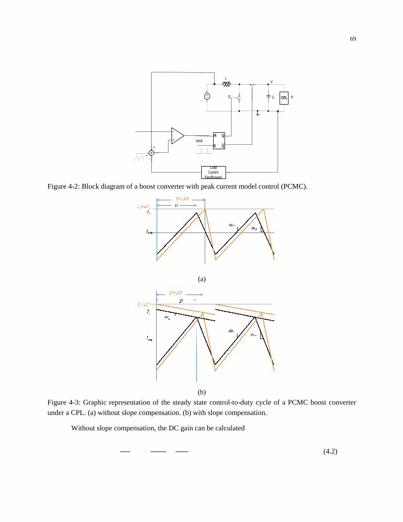
Iramp
Ic
-+
Figure 4-2: Block diagram of a boost converter with peak current model control (PCMC).
Figure 4-3: Graphic representation of the steady state control
under a CPL. (a) without slope compensation. (b) with slope compensation.
Without slope compensation, the DC gain can be calculated
CPLVg
L
C PD
V
R Q
QS
LoadCurrent
Feedforward
Iff
IL
+
clock
Block diagram of a boost converter with peak current model control (PCMC).
(a)
(b)
: Graphic representation of the steady state control-to-duty cycle of a PCMC boost converter
under a CPL. (a) without slope compensation. (b) with slope compensation.
Without slope compensation, the DC gain can be calculated
69
Block diagram of a boost converter with peak current model control (PCMC).
duty cycle of a PCMC boost converter
(4.2)
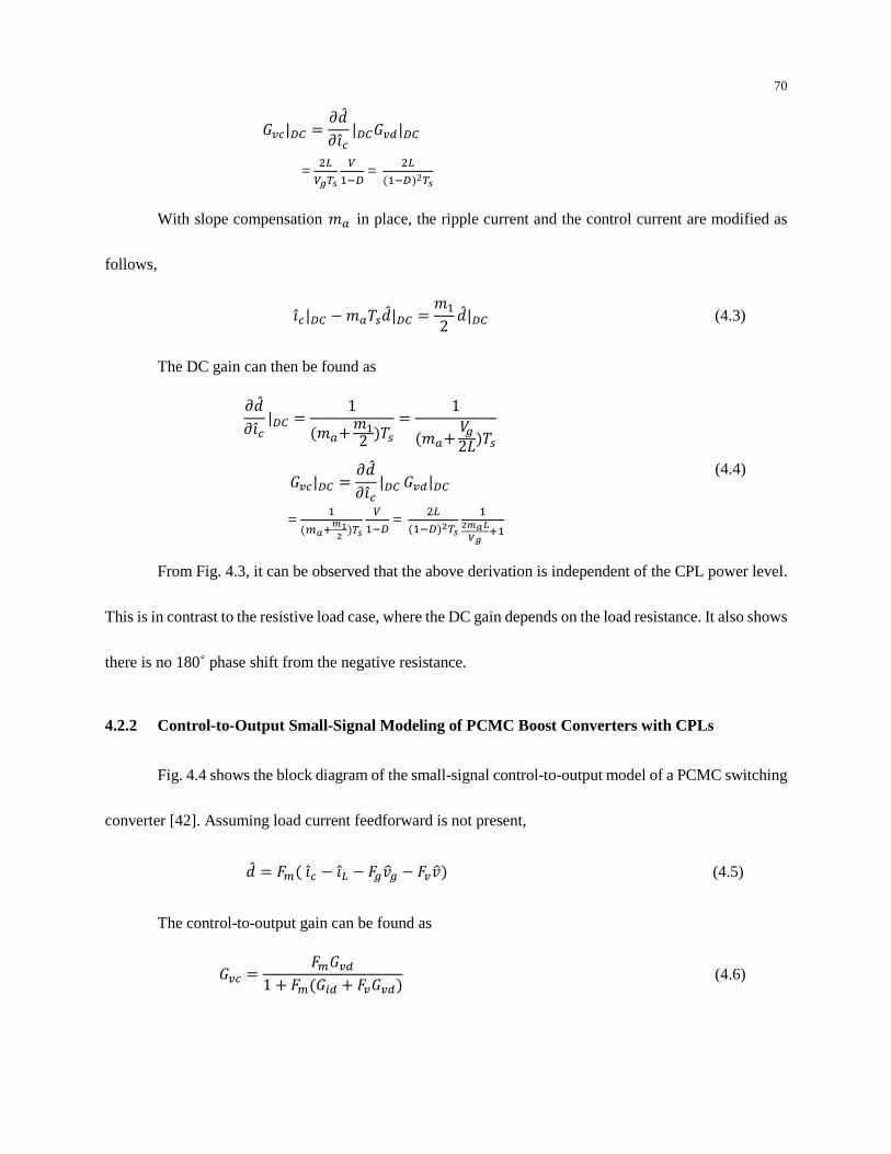
70
`| ¨©¨ |`<|
= ,Yª«¬ ML = ,YML «¬
With slope compensation in place, the ripple current and the control current are modified as
follows,
| ®9©| M2 ©| (4.3)
The DC gain can then be found as
¨©¨ | 1 M2 ®9 1 (2n®9
`| ¨©¨ | `<|
= M¯RO° «¬ML =
,YML «¬ M O¯g±ª RM
(4.4)
From Fig. 4.3, it can be observed that the above derivation is independent of the CPL power level.
This is in contrast to the resistive load case, where the DC gain depends on the load resistance. It also shows
there is no 180˚ phase shift from the negative resistance.
4.2.2 Control-to-Output Small-Signal Modeling of PCMC Boost Converters with CPLs
Fig. 4.4 shows the block diagram of the small-signal control-to-output model of a PCMC switching
converter [42]. Assuming load current feedforward is not present,
© ² Y ²³ ² ³ (4.5)
The control-to-output gain can be found as
` ²`<1 ²< ² `< (4.6)
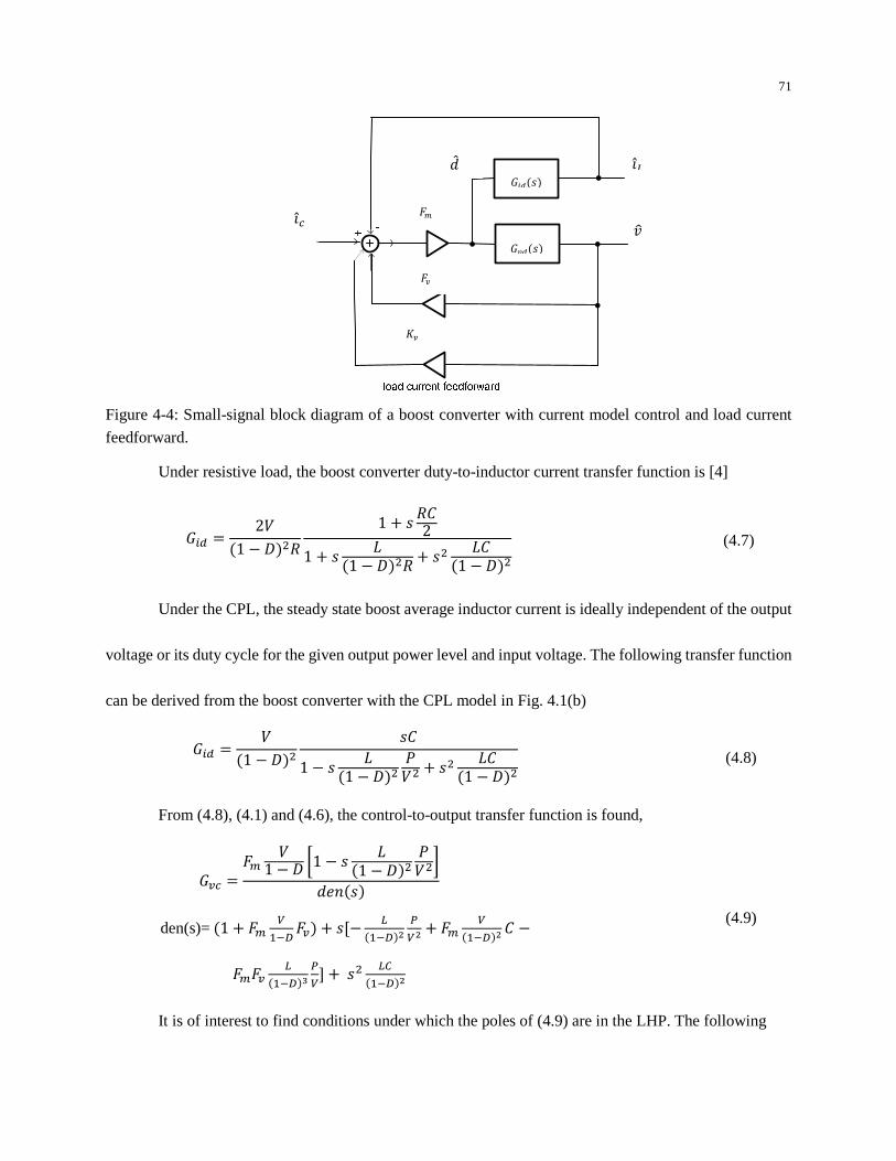
71
Figure 4-4: Small-signal block diagram of a boost converter with current model control and load current
feedforward.
Under resistive load, the boost converter duty-to-inductor current transfer function is [4]
< 2(1 l,X 1 E X821 E n1 l,X E, n81 l, (4.7)
Under the CPL, the steady state boost average inductor current is ideally independent of the output
voltage or its duty cycle for the given output power level and input voltage. The following transfer function
can be derived from the boost converter with the CPL model in Fig. 4.1(b)
< (1 l, E81 E n1 l, (, E, n81 l, (4.8)
From (4.8), (4.1) and (4.6), the control-to-output transfer function is found,
` ² (1 l A1 E n1 l, (,DGE
den(s)= 1 ² ML ² E/ YML t ² ML 8 ²² YML´ t7 E, YML
(4.9)
It is of interest to find conditions under which the poles of (4.9) are in the LHP. The following
<E
`<E
²
²
k`
©
Y
³
72
sufficient and necessary condition has to be maintained for PCMC (i.e. the maximum slope
compensation is restricted):
n1 l, (, ² (1 l, 8 ²² n1 l ( µ 0 (4.10)
If
²(8 ² n1 l ( ¶ n (, (4.11)
and the low-Q approximation in (4.9) is valid, then the ` transfer function at low frequencies can
be approximated as
` ² (1 l A1 E n1 l, (,D$1 ² (1 l ² % E² (1 l, 8 (4.12)
The low frequency gain of ` becomes
`0 ² (1 l1 ² (1 l ² 1 M2 ®9(1 l 2n1 l,®9
12n( 1 (4.13)
which is the same as (4.4), assuming the following current-mode control model gains [4]
² 1®9 , ² 1 l,®92n (4.14)
The low frequency gain for CPLs in (4.13) is the same result as for the unloaded case (R →+∞).
This means that the low frequency gain remains constant in the boost converter with CPL, at any power
level. It is interesting to notice that CPL < in (4.8) doesn’t have a DC term as in the resistive load < in
(4.7). The constant low frequency gain of CPL ` independent of the power levels is the direct
consequence of the non-existing DC term in (4.8).
The ` medium frequency asymptote in (4.12) becomes the same as the equivalent resistive load

73
case:
` 1 l 1 E n1 l, (,E8 (4.15)
From the s-term of the denominator in (4.9), it can be observed that the RHP pole at ML ,=Y t in
`< is shifted to the LHP at M,=·O ML M in ` by the means of PCMC.
It should be noted that different average models ([42], [73]-[76]) use different expressions for ²
and ² , and imply somewhat different high frequency behaviors. In this paper, the high frequency behavior
or sampling effects are not considered. As discussed earlier, under the constant power load, the boost
converter average inductor current over a switching cycle is ideally constant in steady state for a given input
voltage. The expressions (4.14) from [42] are consistent with this observation.
So far, only CCM operation has been considered. It is of interest to examine if PCMC would affect
the CPL instability in DCM (discontinuous-conduction-mode). The PCMC average mode in DCM [42]
indicates the boost switch acts as a power sink equaling to the load power. Therefore, as opposed to CCM
operation, an additional feedback mechanism is required. ` in DCM can also be derived from (4.6).
Since in DCM the inductor current drops to 0 in every switching cycle, there is essentially no inductor
current feedback [77], i.e., < 0. Based on (6) with < 0 in DCM, CMC would not necessarily
imply stability in a DCM boost with CPL.
4.2.3 Load Current Feedforward for PCMC Boost Converters with Resistive Loads
Load current feedforward is a very effective way to improve the boost converter load transient
response. A precise feedforward would set the duty cycle quickly to the target. CMC is naturally suitable
for the load current feedforward as the load current can be precisely translated into the equivalent inductor

74
current from the input and output power relationship. A small-signal model with the load current
feedforward is shown in Fig. 4.4. One possible large-signal feedforward choice is
¸·· ¸ (4.16)
where i is the load current. A small signal perturbation of (4.16) gives
·· ³ ³ ()(, 2 ((³X ³ ()(, 21 l ³X 11 l, ³X (4.17)
Another feedforward choice would be to use the target output voltage (p- instead of the output
voltage
¸·· (p-¸ (4.18)
This choice has drawback of the reference voltage feedforward even though the load current is
fixed. A small signal perturbation of (4.18) gives
·· (p-( ³p- )( ³ (p-)(, ((³X ((
³p-X ³ ()(, 11 l ³ ³p-X 11 l, ³X
(4.19)
From (4.17) and (4.19), we can see that the load current feedforward effectively becomes output
voltage feedback and input voltage feedfoward. It essentially modifies ² and ² in (4.5). To generalize,
the following notation is adopted
·· k`³ kp-³p- k³ (4.20)
With resistive load R, the control-to-output gain becomes
` ² (1 l A1 E n1 l, 1XDGE
den(s)= /1 ² ML ² ,fML k`7 E/ YML Mf ² ML 8 (4.21)

75
²² k` YML´ f7 E,/ YML ²² k` YML¹ f7 It is interesting to note that ` can become unstable if a too strong load current feedforward
(k`>>,fML) is applied. With k`=
,fML (as in (4.17)), the boost converter ` becomes close to that of a
CPL expressed in (4.13) and (4.15).
Comparing (4.21) and (4.9), the load impedance is equivalently increased by the feedforward as
X º X 11 12 k`X1 l (4.22)
And the equivalent load impedance becomes negative if k`>,fML. With perfect feedforward
k`=,fML , the load impedance is tends to infinity, as if the converter were unloaded.
4.2.4 Load Current Feedforward for PCMC Boost Converters with CPLs
As for the resistive load, load current can also be applied for CPLs to improve the boost converter
load transient response. As in the resistive load case, one feedorward choice is given by (4.16).
The small signal perturbation gives
·· ³ ³ ()(, (( ³ (( ³ ³ ()(, (, ³ (4.23)
With this choice, the load current is supply feedforward only without any feedback. As in the
resistive load case, a different feedforward choice would be to use the target output voltage (p- instead of
the output voltage, as given by (4.18). In this case, the small signal perturbation gives
·· (p- ³p- )( ³ (p-)(, (( P³p- ³Q (, ³ (4.24)
From (4.24), we can see that the load current feedforward effectively becomes output voltage

76
feedback, and input and reference voltage feedforward. Also compared with (4.19), (4.24) has negative sign
to the output voltage feedback. To generalize, the following notation is used
·· k`³ kp-³p- k³ (4.25)
With the CPL, the control-to-output gain is
` ² (1 l A1 E n1 l, (,DGE
den(s)= /1 ² ML ² k`7 E/ YML t ² ML 8 ²² k` YML´ t7 E, YML
(4.26)
It can be observed that with load current feedforward present ` with the choice of k=2(21l
becomes similar to the control-to-output response with an equivalent resistive load.
The transfer functions for the resistive loads and CPLs can be calculated and are summarized in
Table 4.1 for the PCMC models.
4.3 Valley Current Mode Control for Boost converters with CPLs
Valley current mode control (VCMC) has an advantage over PCMC in boost applications operating
at low duty cycle, where the inductor current sensing from the switch in PCMC becomes very difficult due
to the associated switching noise. Fig. 4.5 shows a block diagram of a boost converter with valley current
mode control.
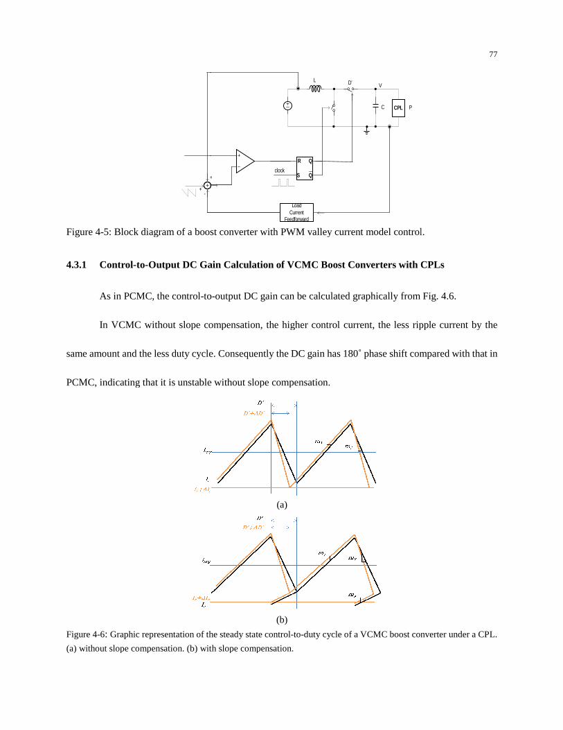
Iramp
IL
Ic
+
-+
Figure 4-5: Block diagram of a boost converter with PWM valley current model control.
4.3.1 Control-to-Output DC Gain Calculation of VCMC Boost Converters with CPLs
As in PCMC, the control-to
In VCMC without slope compensation, the higher control current, the less ripple current by the
same amount and the less duty cycle. Consequently the DC gain has 180
PCMC, indicating that it is unstable without slope compensation.
Figure 4-6: Graphic representation of the steady state control
(a) without slope compensation. (b) with slope compensation.
CPLVg
L
C P
D’ V
R Q
QS
LoadCurrent
Feedforward
Iff
IL
+clock
Block diagram of a boost converter with PWM valley current model control.
Output DC Gain Calculation of VCMC Boost Converters with CPLs
to-output DC gain can be calculated graphically from Fig.
In VCMC without slope compensation, the higher control current, the less ripple current by the
same amount and the less duty cycle. Consequently the DC gain has 180˚ phase shift compared with that in
PCMC, indicating that it is unstable without slope compensation.
(a)
(b)
Graphic representation of the steady state control-to-duty cycle of a VCMC boost converter under
(a) without slope compensation. (b) with slope compensation.
77
Block diagram of a boost converter with PWM valley current model control.
Output DC Gain Calculation of VCMC Boost Converters with CPLs
output DC gain can be calculated graphically from Fig. 4.6.
In VCMC without slope compensation, the higher control current, the less ripple current by the
˚ phase shift compared with that in
boost converter under a CPL.
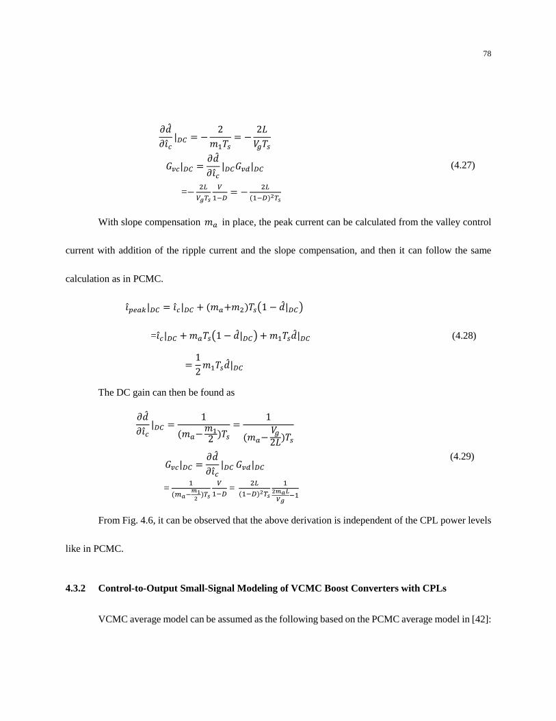
78
¨©¨ | 2M®9 2n(®9
`| ¨©¨ |`<|
= ,Yª«¬ ML ,YML «¬ (4.27)
With slope compensation in place, the peak current can be calculated from the valley control
current with addition of the ripple current and the slope compensation, and then it can follow the same
calculation as in PCMC.
;-| | ,®9P1 ©|Q
=| ®9P1 ©|Q M®9©|
12 M®9©|
(4.28)
The DC gain can then be found as
¨©¨ | 1 M2 ®9 1 (2n®9
`| ¨©¨ | `<|
= M¯LO° «¬ML =
,YML «¬ M O¯g±ª LM
(4.29)
From Fig. 4.6, it can be observed that the above derivation is independent of the CPL power levels
like in PCMC.
4.3.2 Control-to-Output Small-Signal Modeling of VCMC Boost Converters with CPLs
VCMC average model can be assumed as the following based on the PCMC average model in [42]:

79
¸Y ¸ 1 ®9 M2 ,®9
,2 1 ,®9
(4.30)
Correspondingly the small signal model of VCMC becomes:
© ² Y ²³ ² ³ (4.31)
Compared (4.31) with its counterpart (4.5) in PCMC, it is apparent ²³ and ² ³ terms in (4.5)
change sign. Following the same exercise in PCMC, the transfer functions for the resistive loads and CPLs
can be calculated and are summarized in Table 4.2 for the VCMC models.
To make the poles in the LHP based on the calculated `, the relationship in (4.10) and the
additional following have to be maintained:
1 ² ML ² > 0 (4.32)
The above inequality puts additional minimum constraint on the slope compensation to prevent the
sub-harmonic oscillation. The low frequency gain becomes (with ² and ² in (4.14))
`0 ² (1 l1 ² (1 l ²
1 M2 ®9(1 l 2n1 l,®9
12n( 1 (4.33)
This is consistent with the DC gain graphics calculation result in (4.29).
From the s-terms in the denominator of `, it can be observed that the RHP pole at ML ,=Y t in
`< shifted to the LHP at M,=·O ML M in ` by the means of VCMC provided with the assumption of
(4.10) and (4.32).

80
4.3.3 Load Current Feedforward for VCMC Boost Converters with Resistive Loads
As in PCMC, load current feedforward can be applied in VCMC with resistive loads. One possible
feedfoward choice is given by (4.16). Another feedforward choice would be to use the target output voltage
(p- instead of the output voltage, given by (4.18). As in the PCMC, (4.20) is adopted for generalization,
and ` is summarized in Table 4.2.
Like PCMC, ` can become unstable if a too strong load current feedforward (k`>>,fML) is
applied. With k`=,fML (as in (4.17)), the boost converter ` becomes close to that of a CPL expressed
in (4.13) and (4.15).
4.3.4 Load Current Feedforward for VCMC Boost Converters with CPLs
Load current can also be applied for CPLs to improve the boost converter load transient response.
As in the previous cases, one possible feedforward choice is by (4.16). Another feedforward choice would
be to use the target output voltage (p- instead of the output voltage, given by (4.18). To generalize, the
notation in (4.24) is adopted, and ` is summarized in Table 4.2.
Like PCMC, with load current feedforward present, ` with the choice of k=2(21l becomes
similar to the control-to-output response with an equivalent resistive load.
4.4 Simulation Results
The PCMC and VCMC models for the boost converters under CPLs have been validated by
Simplis [87] simulations, including small-signal frequency responses derived from the transient responses
[87]-[89]. Closed-loop PCMC and VCMC boost converters were simulated under conditions of Vg = 3 V,

81
V = 4 V, and fsw = 5.4 MHz with L = 1 µH and C = 4.7 µF, and the deadbeat slope compensation. The
voltage loop compensations follow the standard schemes used in the CMC with resistive load, such as in
[81] and [86], as CMC makes ` under CPL similar to ` under resistive load as demonstrated in Table
4.1 and Table 4.2.
In the simulations, the CPLs were implemented by the table models, where the output voltages and
currents are numerically tabulated for the loads. Fig. 4.7(a) and Fig. 4.8(a) show the simulated
control-to-output transfer functions along with the models for PCMC and VCMC respectively for light and
heavy CPLs. Fig. 4.7(b) and Fig. 4.8(b) show the simulated ` with the load current feedforward based on
(4.18) for PCMC and VCMC respectively. The simulated transfer functions match the model predictions
very well for frequency up to 0.2 fsw. Without the load current feedforward, the ` low frequency gains
under the different power levels are close to those of unloaded conditions as shown in Fig. 4.7(a) and Fig.
4.8(a). The RHP zero under heavy load remains at the same location as in the converter with an equivalent
resistive load.
Under the light CPL condition, the ` transfer function with the load current feedforward is
similar to the response without the load current feedforward, as the feedforward amount is negligible in
(4.18). Under the heavy CPL condition, the ` low frequency gain with the load current feedforward is
much lower than without feedforward. The transfer functions for the CPLs with load current feedforward
behave more like the transfer functions with resistive loads. This can also be seen from Table 4.1 and Table
4.2.

82
Table 4.1: CMC boost control-to-output `small-signal model with resistive loads
PCMC VCMC < 2(1 l,X 1 E X821 E n1 l,X E, n81 l,
` ` ² (1 l A1 E n1 l, 1XDGE
den(s)= /1 ² ML ² ,fML7 E/ YML Mf
² ML 8 ²² YML´ f7 E,/ YML ²² YML¹ f7
` ² (1 l A1 E n1 l, 1XDGE
den(s)= /1 ² ML ² ,fML7 E/ YML Mf
² ML 8 ²² YML´ f7 E,/ YML ²² YML¹ f7
`with
load current
feedforward
` ² (1 l A1 E n1 l, 1XDGE
den(s)= /1 ² ML ² ,fML k`7 E/ YML Mf
² ML 8 ²² k` YML´ f7 E,/ YML ²² k` YML¹ f7
` ² (1 l A1 E n1 l, 1XDGE
den(s)= /1 ² ML ² ,fML k`7 E/ YML Mf
² ML 8 ²² k` YML´ f7 E,/ YML ²² k` YML¹ f7

83
Table 4.2: CMC boost control-to-output `small-signal model with constant power loads
PCMC VCMC < (1 l, E81 E n1 l, (2 E, n81 l,
` ` ² (1 l A1 E n1 l, (,DGE
den(s)= 1 ² ML ² E/ YML t ² ML 8 ²² YML´ t7 E, YML
` ² (1 l A1 E n1 l, (,DGE
den(s)= 1 ² ML ² E/ YML t ² ML 8 ²² YML´ t7 E, YML
` with
load current
feedforward
` ² (1 l A1 E n1 l, (,DGE
den(s)= /1 ² ML ² k`7 E/ YML t ² ML 8 ²² k` YML´ t7 E, YML
` ² (1 l A1 E n1 l, (,DGE
den(s)= /1 ² ML ² k`7 E/ YML t ² ML 8 ²² k` YML´ t7 E, YML
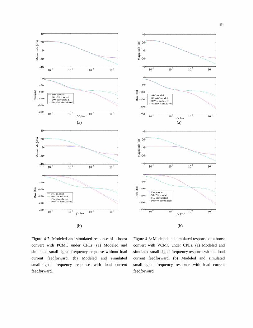
84
TABLE II CMC boost control-to-output `small-signal model with constant power loads
PCMC VCMC < (1 l, E81 E n1 l, (2 E, n81 l,
` ` ² (1 l A1 E n1 l, (,DGE
den(s)= 1 ² ML ² E/ YML t ² ML 8
²² YML´ t7 E, YML
` ² (1 l A1 E n1 l, (,DGE
den(s)= 1 ² ML ² E/ YML t ² ML 8 ²² YML´ t7
E, YML
`with load
current
feedforwar
d
` ² (1 l A1 E n1 l, (,DGE
den(s)= /1 ² ML ² k`7 E/ YML t ² ML 8 ²²
k` YML´ t7 E, YML
` ² (1 l A1 E n1 l, (,DGE
den(s)= /1 ² ML ² k`7 E/ YML t ² ML 8
²² k` YML´ t7 E, YML
In the simulations, the CPLs were implemented by the table models, where the output voltages and
currents are numerically tabulated for the loads. Fig. 7(a) and Fig. 8(a) show the simulated control-to-output
transfer functions along with the models for PCMC and VCMC respectively for light and heavy CPLs in
CCM operations. Fig. 7(b) and Fig. 8(b) show the simulated `with the load current feedforward based on
(a)
(b)
Figure 4-7: Modeled and simulated response of a boost
convert with PCMC under CPLs. (a) Modeled and
simulated small-signal frequency response without load
current feedforward. (b) Modeled and simulated
small-signal frequency response with load current
feedforward.
10-4
10-3
10-2
10-1-40
-20
0
20
40M
agn
itud
e (
dB
)
10-4
10-3
10-2
10-1-250
-200
-150
-100
-50
0
f / fsw
Phase
(deg)
8W model80mW model8W simulated80mW simulated
10-4
10-3
10-2
10-1-40
-20
0
20
40
Mag
nitu
de
(d
B)
10-4
10-3
10-2
10-1-250
-200
-150
-100
-50
0
f / fsw
Phase
(deg)
8W model80mW model8W simulated80mW simulated
(a)
(b)
Figure 4-8: Modeled and simulated response of a boost
convert with VCMC under CPLs. (a) Modeled and
simulated small-signal frequency response without load
current feedforward. (b) Modeled and simulated
small-signal frequency response with load current
feedforward.
10-4
10-3
10-2
10-1-40
-20
0
20
40
Ma
gnitu
de (
dB)
10-4
10-3
10-2
10-1-250
-200
-150
-100
-50
0
f / fsw
Phase
(deg)
8W model80mW model8W simulated80mW simulated
10-4
10-3
10-2
10-1-40
-20
0
20
40
Ma
gnitu
de (
dB)
10-4
10-3
10-2
10-1-250
-200
-150
-100
-50
0
f / fsw
Phase
(deg)
8W model80mW model8W simulated80mW simulated
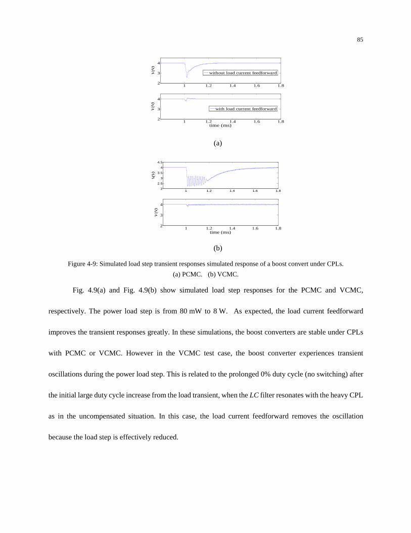
85
(a)
(b)
Figure 4-9: Simulated load step transient responses simulated response of a boost convert under CPLs.
(a) PCMC. (b) VCMC.
Fig. 4.9(a) and Fig. 4.9(b) show simulated load step responses for the PCMC and VCMC,
respectively. The power load step is from 80 mW to 8 W. As expected, the load current feedforward
improves the transient responses greatly. In these simulations, the boost converters are stable under CPLs
with PCMC or VCMC. However in the VCMC test case, the boost converter experiences transient
oscillations during the power load step. This is related to the prolonged 0% duty cycle (no switching) after
the initial large duty cycle increase from the load transient, when the LC filter resonates with the heavy CPL
as in the uncompensated situation. In this case, the load current feedforward removes the oscillation
because the load step is effectively reduced.
1 1.2 1.4 1.6 1.82
3
4
V (V)
1 1.2 1.4 1.6 1.82
3
4
time (ms)
V (V)
with load current feedforward
without load current feedforward
1 1.2 1.4 1.6 1.82
2.5
3
3.5
4
4.5
V(V
)
1 1.2 1.4 1.6 1.82
3
4
time (ms)
V (V)
86
4.5 Summary
In this chapter, current mode control is examined for the boost converters with constant power
loads (CPLs). By small-signal modeling it is shown how peak current mode control (PCMC) and valley
current mode control (VCMC) provide active damping, effectively removing the RHP poles due to CPLs.
Load current feedforward is also analyzed in the small-signal models. Small-signal frequency responses
and transient simulations validate the analysis results. The simulations demonstrate stable operations of
current-mode controlled boost converters under CPLs. It is further shown how load current feedforward
improves CPL step responses and removes transient oscillations present in the VCMC without feedforward.
87
Chapter 5
Multi-Mode RF PA Supply Design
In Section3.2.3, a buck/boost and class-B linear amplifier (LDO) series architecture is proposed as
the multi-mode PA supply. This architecture shown in Fig. 5.1 is capable of GSM, linear EDGE, polar
EDGE, and linear WCDMA/HSPA operations. This chapter focuses on the key design aspects in detail of
the major blocks of the architecture, including the buck/boost, the wideband LDO and the PA bias LDO.
Figure 5-1: Block diagram of a multi-mode PA supply with series LAS architecture.

88
5.1 Buck/Boost Converter
The buck/boost converter has two major control blocks: the PWM generation block and the error
amplifier. Other than the output switches, it has supporting blocks including reference, oscillator, current
limit, zero crossing sensing, and gate driver with the dead time control.
5.1.1 Buck or Boost PWM
Fig. 5.2 shows the four-switch non-inverting buck/boost architecture with the voltage-mode PWM
control. The converter is configured as either a two-switch buck or a two-switch boost converter with the
special care in the buck and boost transition. When it is in the buck mode, the boost side switches are not
switching. Similarly when in the boost mode, the buck side switches are not switching. This has advantage
of having lower inductor current compared with a simplified traditional control with four switches
switching (a pair switching at the same time during DTs and another pair switching during (1-D)Ts).
89
Figure 5-2: A buck or boost architecture with voltage mode control sharing a single error amplifier.
The control scheme has been widely used [90]-[91]. The converter has a single error amplifier (EA)
with two PWM comparators. In this control scheme, a predetermined threshold level Vm (also the PWM
saw-tooth ramp height) is in place to decide if the buck or boost loop should be in control. If the control
voltage Vc (EA output) is higher than the threshold, the boost loop is in control, otherwise the buck loop is in
control.
Near 100% buck or 0% boost uniform switching duty cycle is difficult to achieve with a standalone
buck or boost converter due to the finite switching dead time introduced to overcome the output devices
shoot-through. In these conditions the regulation is achieved naturally from the control loop by modulating
90
a few cycles of 100% buck (or 0% boost) with a lower (or higher in the boost case) achievable duty cycle.
However the switching ripple is much larger and chaotic due to the low frequency modulation content. This
sub-harmonic phenomenon is sometimes called “pulse-skipping”.
This “pulse-skipping” issue can be largely resolved with four switches in place. One way is to apply
the traditional buck/boost single loop control scheme with four switches switching at near 50% duty cycle
during the buck and boost transition. This will require higher inductor current. Another way without
increasing the inductor current is to mix a high buck duty with a low boost duty followed in a controlled
manner [91]. Because of the mixing is at the switching rate, no low frequency large ripple exists. Table 5.1
illustrates the concept. Assuming buck has pulse-skipping between 97% and 100% duty cycle and boost has
pulse-skipping between 0% and 3% duty cycle, the equivalent duty cycle can be achieved with a lower duty
buck and higher boost to eliminate the pulse-skipping. To avoid the loop gain change at the mixing window
edges, the equivalent average duty of the two adjacent buck and boost mixing cycles should be equal to the
desired buck or boost duty cycle. For example, average duty of 91% buck and 3% boost is equivalent to 97%
buck duty.
Table 5.1: Buck and Boost mixing to achieve equivalent Buck or Boost
Desired buck duty 97% 98% 99% 100% 100% 100% 100%
Desired boost duty 0% 0% 0% 0% 1% 2% 3%
Buck duty in mixing 91% 92% 93% 94% 95% 96% 97%
Boost duty in mixing 3% 4% 5% 6% 7% 8% 9%
This buck and boost cycle mixing or dithering can be controlled by introducing a small amount of
offset with opposite polarity to the two control inputs of the PWM comparators as shown in Fig. 5.3. An
91
accurate sense and control for the buck and boost mixing window edge is needed to determine when the
mixing should be activated. This can be achieved by monitoring the control voltage level. There is a 1-to-1
linear mapping between the static control voltage and the duty cycle, once the control voltage threshold of
the buck/boost transition and the minimum PWM ramp level are determined.
Figure 5-3: Buck or boost architecture with out-of-phase triangle waveforms as PWM ramps.
Fig. 5.4 shows the timing diagram of the key signals of the proposed scheme during the buck and
boost transition. The buck and boost duty cycles are mixed by the offsets introduced to the PWM
comparators. In order to accurately define the mixing boundary conditions, the output of phase triangular
92
waveforms need to be well controlled. The details of the way to create them are described in the
oscillator design of Section 5.1.3. The triangular waveforms create the dual-edge type of PWM. The
triangular level is set to well above the ground, so that a very low switching duty cycle is made possible.
This is unlike the typical voltage mode controller with a saw tooth ramp signal with its minimum at the
ground.
Figure 5-4: PWM waveforms to illustrate the buck and boost mixing in the transition region.
5.1.2 Error Amplifier
Fig. 5.5 shows the block diagram of the voltage-mode buck/boost linearized small signal feedback
loop. The transfer function Gvd of the power stage can be derived by the average model [42] and is given in
Table 2.2.
93
Figure 5-5: Small signal block diagram of a buck/boost converter with voltage mode control.
The loop gain of the feedback loop is
®E »EE`<E 1( (5.34)
And the output tracking accuracy is
Ep-E E`<E 1(1 E`<E 1( (5.35)
The error amplifier (EA) is the most critical among all the blocks affecting the converter dynamic
response. Fig. 5.6 shows the EA architecture for the buck/boost. It is a two-stage amplifier with the Miller
compensation. The 1st stage is folded cascode for the wide input common mode range. The dominant pole is
from the Miller capacitor. The amplifier also introduced two zeroes to cancel the double pole from the
output stage. One zero is introduced by the 1st stage degeneration resistor and associated capacitor, and the
2nd zero is introduced by the Miller capacitor with a series resistor (also nulling the RHP zero from the
Miller feed-forward path).
94
Figure 5-6: Buck/boost error amplifier architecture.
This EA is compensated for the buck and boost continuous conduction mode (CCM) operations,
and the low power buck discontinuous conduction mode (DCM). In the buck DCM PWM mode, the NMOS
switch is turned off once the inductor current zero crossing is sensed, and the switching node SW1 is in
tristate. By doing this, the light load efficiency is improved with the reduced conduction loss. The
switching loss in the low power DCM can also be reduced by switching only part of the output switches, to
balance the switching and conduction losses.
A non-linear accumulation capacitor is purposely chosen for the Miller compensation. It has
strong voltage coefficient and configured such that the full capacitance appears in the boost mode and less
in the buck mode. By doing this, the buck loop bandwidth is set higher than the boost loop bandwidth. The
reason is that the boost converter has a RHP zero, and the RHP zero has to be located at much higher
frequency than its loop cross-over frequency, otherwise the loop would not be stable. If a constant Miller

95
capacitance is used, the buck loop bandwidth would be lower and thus much less optimal.
For the DCM compensation, much higher capacitance is switched in from the 1st stage to move its
zero location to a much lower frequency. This is to overcome the much lower frequency output pole once
the converter enters into DCM.
Fig. 5.7 shows the simulated typical loop gain frequency response after compensation with the
average model under boost, buck CCM and buck DCM conditions. The output conditions are 4.8 V with 5Ω
load, 2.26 V with 5 Ω, and 0.85V with 200 Ω respectively under the 3.6 V input at room temperature and
typical process. The simulated bandwidths are 75 kHz, 109 kHz, and 10 kHz respectively.
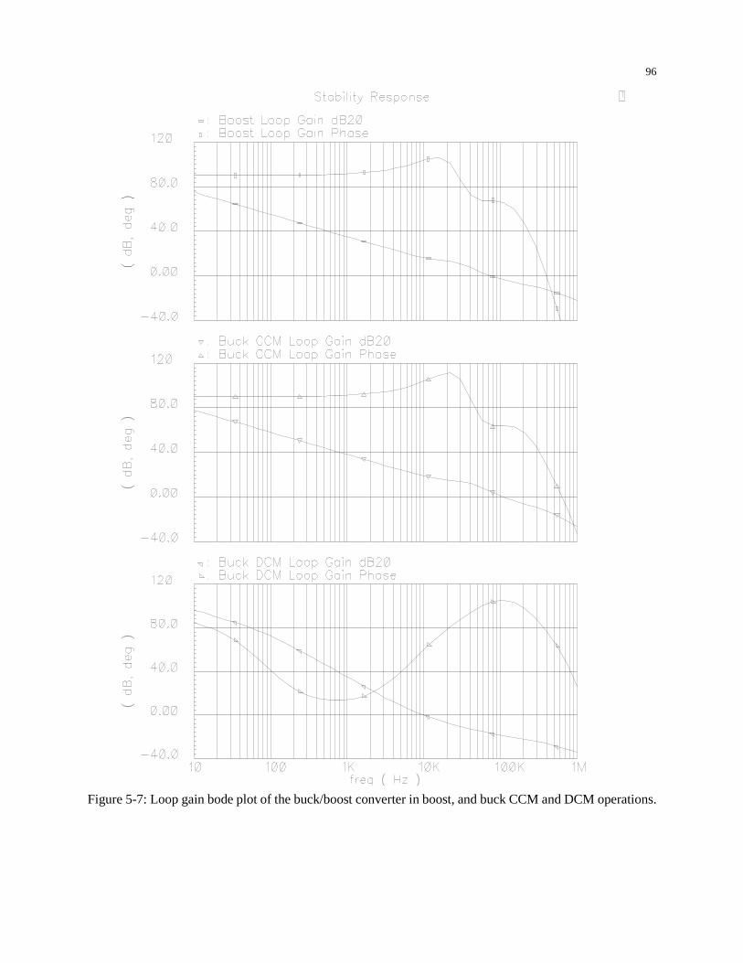
96
Figure 5-7: Loop gain bode plot of the buck/boost converter in boost, and buck CCM and DCM operations.

97
5.1.3 Oscillator
The oscillator is required for a switching converter to control the switching frequency. It is often
tied closely to the PWM comparator(s). In this buck/boost design, the oscillator creates two out-of-phase
triangular waveforms as the inputs of the two PWM comparators. They need to be well controlled as
indicated in Section 5.1.1, in order to accurately define when to turn on or off the buck and boost mixing.
The oscillator architecture is shown in Fig. 5.8, similar to [13]. It has the two desirable properties: 1)
two matched outputs out of phase; 2) well controlled center, and peak or valley levels. A triangular
waveform can be generated by charging or discharging a capacitor until it reaches its low or high reference.
In order to generate the two matched outputs, the charging or discharging current sources are shared. To
make them out-of-phase, one capacitor is charged while the other capacitor is discharged, and their
common mode is controlled by their common mode feedback loop. The switching frequency is determined
by the capacitance, the bias current and the reference levels.
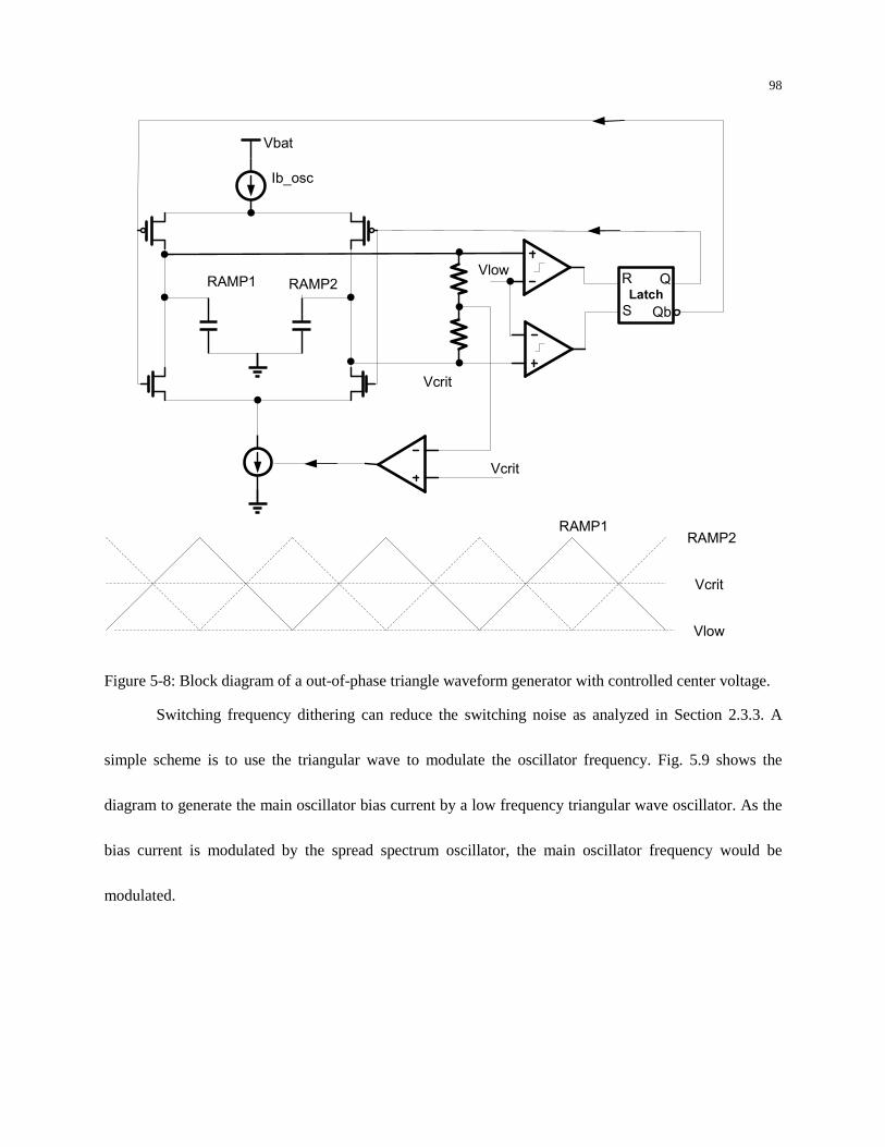
98
Vbat
Latch
Vcrit
VlowR
S
Q
Qb
RAMP1RAMP2
Vcrit
Vcrit
Vlow
RAMP1 RAMP2
Ib_osc
Figure 5-8: Block diagram of a out-of-phase triangle waveform generator with controlled center voltage.
Switching frequency dithering can reduce the switching noise as analyzed in Section 2.3.3. A
simple scheme is to use the triangular wave to modulate the oscillator frequency. Fig. 5.9 shows the
diagram to generate the main oscillator bias current by a low frequency triangular wave oscillator. As the
bias current is modulated by the spread spectrum oscillator, the main oscillator frequency would be
modulated.
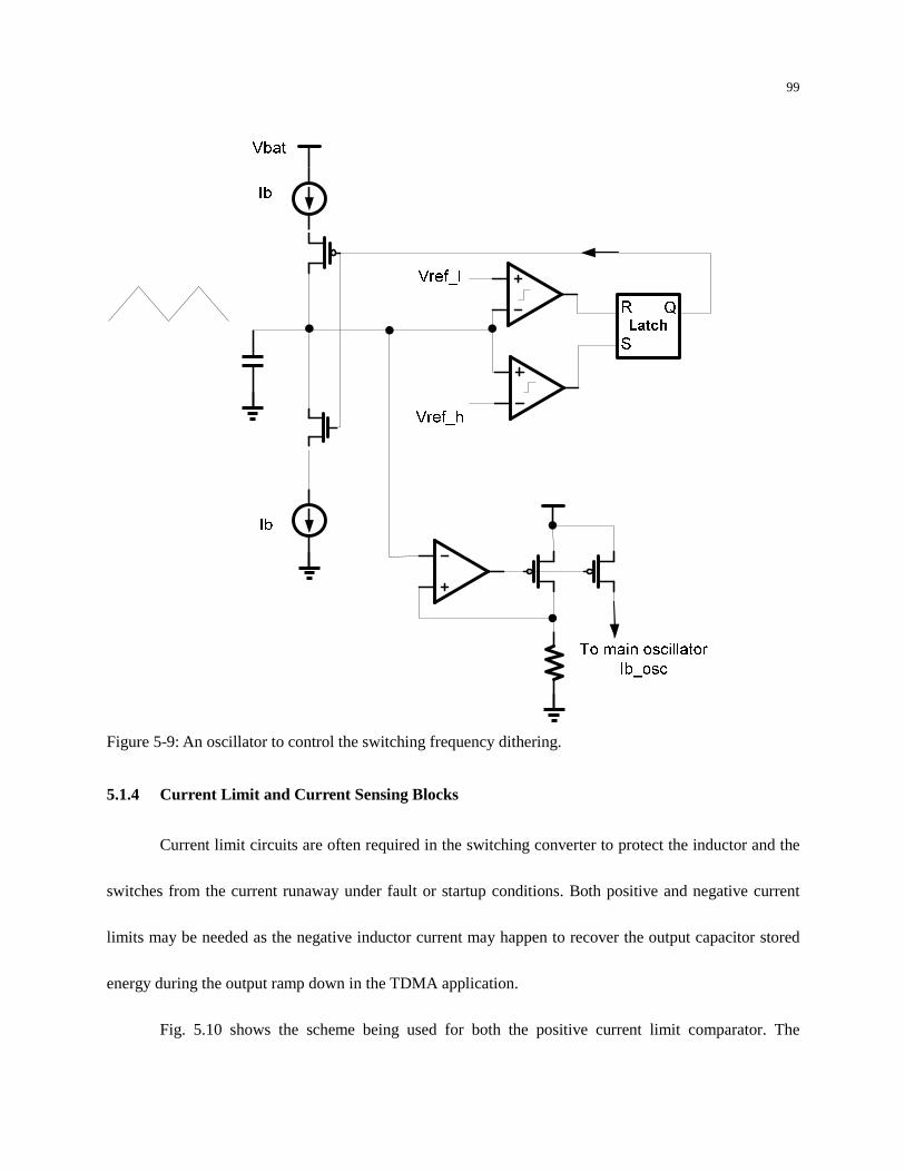
99
Figure 5-9: An oscillator to control the switching frequency dithering.
5.1.4 Current Limit and Current Sensing Blocks
Current limit circuits are often required in the switching converter to protect the inductor and the
switches from the current runaway under fault or startup conditions. Both positive and negative current
limits may be needed as the negative inductor current may happen to recover the output capacitor stored
energy during the output ramp down in the TDMA application.
Fig. 5.10 shows the scheme being used for both the positive current limit comparator. The
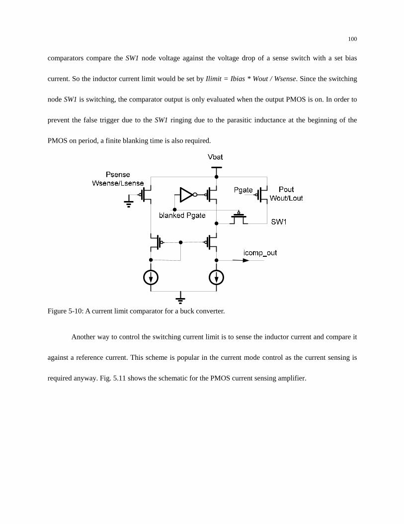
100
comparators compare the SW1 node voltage against the voltage drop of a sense switch with a set bias
current. So the inductor current limit would be set by Ilimit = Ibias * Wout / Wsense. Since the switching
node SW1 is switching, the comparator output is only evaluated when the output PMOS is on. In order to
prevent the false trigger due to the SW1 ringing due to the parasitic inductance at the beginning of the
PMOS on period, a finite blanking time is also required.
Figure 5-10: A current limit comparator for a buck converter.
Another way to control the switching current limit is to sense the inductor current and compare it
against a reference current. This scheme is popular in the current mode control as the current sensing is
required anyway. Fig. 5.11 shows the schematic for the PMOS current sensing amplifier.
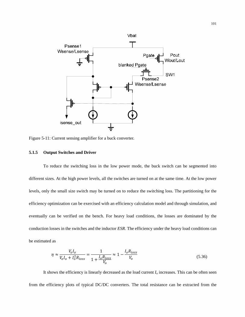
101
Figure 5-11: Current sensing amplifier for a buck converter.
5.1.5 Output Switches and Driver
To reduce the switching loss in the low power mode, the buck switch can be segmented into
different sizes. At the high power levels, all the switches are turned on at the same time. At the low power
levels, only the small size switch may be turned on to reduce the switching loss. The partitioning for the
efficiency optimization can be exercised with an efficiency calculation model and through simulation, and
eventually can be verified on the bench. For heavy load conditions, the losses are dominated by the
conduction losses in the switches and the inductor ESR. The efficiency under the heavy load conditions can
be estimated as
()() ),Xo99 11 )Xo99( 1 )Xo99( (5.36)
It shows the efficiency is linearly decreased as the load current Io increases. This can be often seen
from the efficiency plots of typical DC/DC converters. The total resistance can be extracted from the

102
efficiency plot from the negative slop of η vs Io. (5.36) also shows the efficiency decreases as the output
voltage drops for the same load current.
When the load current is getting lower and lower, the switching losses are getting closer to the
conduction losses, (5.36) is no longer valid. When the output power is very low, the switching losses will be
dominated, and thus the efficiency would be getting lower for the low power conditions. The total losses are
estimated as
o99 )Y,X<9,t X<9,u XY ()YΔ.wxyz|~9 12 8-(,~9 (<<-)YΔ.y|~9 )q( Y,X
(5.37)
As we can see from the above expression, if the device is too big, the switch losses will dominate
due to the big gate capacitance and long overlap time of voltage and current across the switching devices; if
the device size is too small, the conduction loss will dominate. For each given output power level, the total
losses can be optimized with the optimal device size choice. Ideally the output switch size can be
continuously adjusted or discretized with fine resolution. In practice, there are usually only a few sizes to
save the number of drivers.
The switching dead time control is critical for the high switching frequency operation and the
efficiency optimization. Adaptive dead time control attempts to reduce the dead time as much as possible
while still maintain the output switch shoot-through free [92]. As the output device is very big, the driver
can also be large. To further reduce the pre-driver shoot-though losses, the pre-driver can also have the
built-in dead time control.
103
5.2 Wideband VCC LDO
This LDO is a Class-B type without a sink device. The output sinking is handled out by the load
itself. Compared with a Class-AB linear amplifier used in current mode parallel LAS, this saves the
quiescent current and the loss associated with the sink device. This LDO needs to handle the GSM/EDGE
time mask and the polar EDGE bandwidth requirements. The 3-dB bandwidth is set in the range of
1-10 MHz.
The input of this LDO (source of the output PMOS) is from the buck/boost output, which has wide
range for the PA power control purpose. This is different from a conventional LDO with a fixed supply.
When the LDO input Vswicther is much higher than the battery voltage Vbat (by PMOS threshold |Vtp|), the
output PMOS cannot be turned on. To overcome this, the maximum of Vswitcher and Vbat is switched in as
the supply for the LDO control amplifier.
When Vswicther is too low (< |Vtp| ), the output PMOS cannot be turned off. To overcome this, a
parallel output NMOS is used, which needs to be regulated as well. LDO output device is often times
PMOS type for simplicity. NMOS can also be used as the output device, but often requires a charge pump
or additional supply for its gate control [94]-[96]. Fig. 5.12(a) shows the LDO architecture with a PMOS
and a NMOS in parallel as the output devices. The two control loops share the single error amplifier. The
PMOS loop has two gain stages with the folded casocode as the 1st gain stage for the wide input common
mode range, and the output as the 2nd gain stage (shown in Fig. 5.12(b)). The NMOS loop has the folded
cascode as the only gain stage, and the output stage is a unit-gain source follower. Because of the gain stage
difference, switches are used to select the 1st stage output.
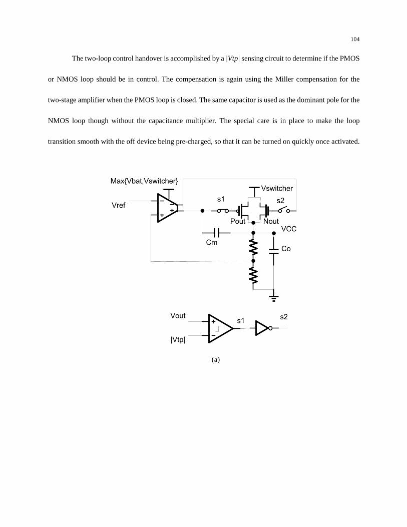
104
The two-loop control handover is accomplished by a |Vtp| sensing circuit to determine if the PMOS
or NMOS loop should be in control. The compensation is again using the Miller compensation for the
two-stage amplifier when the PMOS loop is closed. The same capacitor is used as the dominant pole for the
NMOS loop though without the capacitance multiplier. The special care is in place to make the loop
transition smooth with the off device being pre-charged, so that it can be turned on quickly once activated.
VCC
Vswitcher
Vref
CmCo
MaxVbat,Vswitcher
s1 s2
s1s2Vout
|Vtp|
Pout Nout
(a)
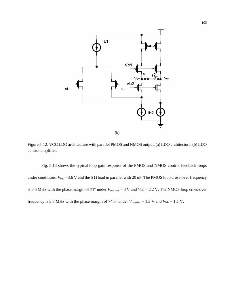
105
(b)
Figure 5-12: VCC LDO architecture with parallel PMOS and NMOS output. (a) LDO architecture, (b) LDO
control amplifier.
Fig. 5.13 shows the typical loop gain response of the PMOS and NMOS control feedback loops
under conditions: Vbat = 3.6 V and the 5 Ω load in parallel with 20 nF. The PMOS loop cross-over frequency
is 3.5 MHz with the phase margin of 71° under Vswicther = 3 V and Vcc = 2.2 V. The NMOS loop cross-over
frequency is 5.7 MHz with the phase margin of 74.5° under Vswicther = 1.3 V and Vcc = 1.1 V.
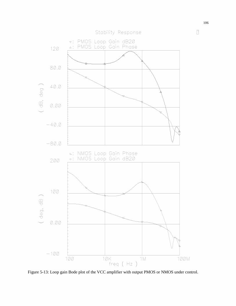
106
Figure 5-13: Loop gain Bode plot of the VCC amplifier with output PMOS or NMOS under control.
107
The tracking LDO has two control loops with the shared error amplifier. The two control loops
have different output devices. In order to have the fast transition, the off device is pre-biased so that it can
be turned on quickly. There is trade-off between the response quickness and the leakage current. The fast
response will result in higher leakage. Fig. 5.14 shows the schematic of a different approach. In this design,
the NMOS loop has two gain stages followed by the NMOS source follower. When the output PMOS is in
regulation, the NMOS is biased off, which is achieved through the stronger bias current Ib than the mirrored
output current from M2.
Figure 5-14: VCC amplifier with smooth transition between the output PMOS and NMOS control loops.
This new approach will not only get rid of the transition glitch, but it will also eliminate the loop
sensing and leakage control circuit. Additionally, no switches are needed at the outputs of the error
amplifier, because both loops now have two gain stages. Fig. 5.15 and Fig. 5.16 compare the simulated
waveforms of the two approaches. Fig. 5.15 shows an exaggerated condition with a large Vswitcher sweep to
catch the glitch. In the real application, Vswitcher is regulated once the buck/boost reference is commanded, so
the Vcc glitch only happens at the particular Vswitcher level. Fig. 5.16 shows no visible Vcc regulation glitches
108
of the new approach when the LDO input Vswitcher changes from 4 V down to 0.8 V and back to 4 V. The gate
waveforms of the output devices are also shown. We can also see the loop transition happens at different
Vswitcher level as well. In the old approach, the loop transition happens around Vswicther = |Vtp| from the Vtp
sensing circuitry. In the new approach, the loop transition happens around Vswicther = Vbat, when the NMOS
gate drive is higher enough to turn on the output NMOS. The new approach shows superior performance.
Figure 5-15: LDO waveforms of LDO architecture with switched PMOS and NMOS control loop. The
glitches can be seen from the PMOS and NMOS gates and the output during the loop transition.
109
Figure 5-16: LDO waveforms of LDO architecture with smooth PMOS and NMOS control loop transition.
No glitches can be seen from the PMOS and NMOS gates and the output during the loop transition.
The new loop gain response is shown in Fig. 5.17. The cross-over frequency is about 2.1 MHz with
the phase margin of 53°.
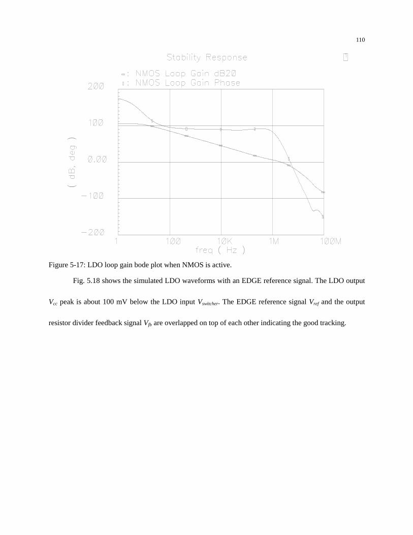
110
Figure 5-17: LDO loop gain bode plot when NMOS is active.
Fig. 5.18 shows the simulated LDO waveforms with an EDGE reference signal. The LDO output
Vcc peak is about 100 mV below the LDO input Vswitcher. The EDGE reference signal Vref and the output
resistor divider feedback signal Vfb are overlapped on top of each other indicating the good tracking.
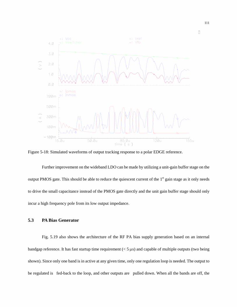
111
Figure 5-18: Simulated waveforms of output tracking response to a polar EDGE reference.
Further improvement on the wideband LDO can be made by utilizing a unit-gain buffer stage on the
output PMOS gate. This should be able to reduce the quiescent current of the 1st gain stage as it only needs
to drive the small capacitance instead of the PMOS gate directly and the unit gain buffer stage should only
incur a high frequency pole from its low output impedance.
5.3 PA Bias Generator
Fig. 5.19 also shows the architecture of the RF PA bias supply generation based on an internal
bandgap reference. It has fast startup time requirement (< 5 µs) and capable of multiple outputs (two being
shown). Since only one band is in active at any given time, only one regulation loop is needed. The output to
be regulated is fed-back to the loop, and other outputs are pulled down. When all the bands are off, the
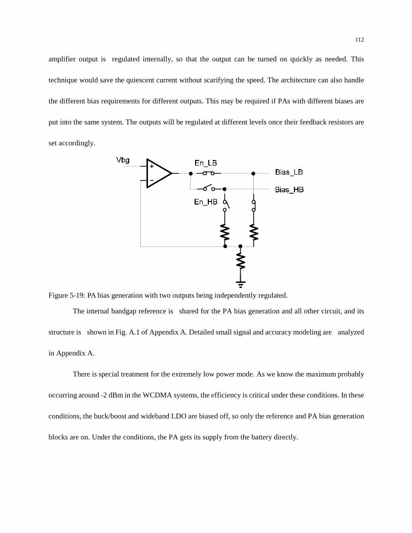
112
amplifier output is regulated internally, so that the output can be turned on quickly as needed. This
technique would save the quiescent current without scarifying the speed. The architecture can also handle
the different bias requirements for different outputs. This may be required if PAs with different biases are
put into the same system. The outputs will be regulated at different levels once their feedback resistors are
set accordingly.
Figure 5-19: PA bias generation with two outputs being independently regulated.
The internal bandgap reference is shared for the PA bias generation and all other circuit, and its
structure is shown in Fig. A.1 of Appendix A. Detailed small signal and accuracy modeling are analyzed
in Appendix A.
There is special treatment for the extremely low power mode. As we know the maximum probably
occurring around -2 dBm in the WCDMA systems, the efficiency is critical under these conditions. In these
conditions, the buck/boost and wideband LDO are biased off, so only the reference and PA bias generation
blocks are on. Under the conditions, the PA gets its supply from the battery directly.

113
5.4 Experimental Results for the Multi-Mode RF PA Supply
In this section, experimental results for the multi-mode PA power supply are given. The buck/boost
results are given first, and followed by those for the LDOs. The evaluation of the power supply combined
with the multi-mode PA is reported afterwards.
Fig. 5.20 shows the microphotograph of the test chip with the proposed multi-mode PA supply. It
has been fabricated in a standard 0.5 µ, 5 V CMOS process, and occupies about 4.8 mm2. The chip total
quiescent current is about 1.1mA with all the blocks enabled under no switching and no load conditions.
The test chip also contains a digital serial interface for programmability, testing and trimming.
Figure 5-20: Die microphotograph of the test chip.
5.4.1 Experimental Results of the Buck/Boost Switcher
Fig. 5.21 shows typical converter switching waveforms under the boost condition with
Vbat = 2.5 V, Vswicther = 5 V, and I load = 800 mA. The inductor current is around 2A. Fig. 5.22(a) shows the
typical PWM CCM load transient waveforms under Vbat = 3.5 V and Vswicther = 1.2 V with a 500mA load step.
The peak-peak transient is about -20 mV / +10 mV. Fig. 5.22(b) shows the typical load transient waveforms
VCC
LDO
bias
LDDigital
IF
buck
boost
switchbuck
boost
control reference
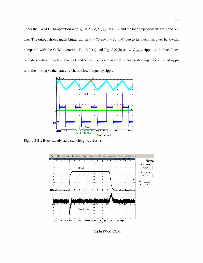
114
under the PWM DCM operation with Vbat = 2.5 V, Vswitcher = 1.2 V and the load step between 9 mA and 500
mA. The output shows much bigger transient (- 75 mV / + 50 mV) due to its much narrower bandwidth
compared with the CCM operation. Fig. 5.22(a) and Fig. 5.22(b) show Vswicther ripple at the buck/boost
boundary with and without the buck and boost mixing activated. It is clearly showing the controlled ripple
with the mixing vs the naturally chaotic low frequency ripple.
Figure 5-21: Boost steady state switching waveforms.
(a) In PWM CCM.
Vswitcher
Iload
SW1
Iind
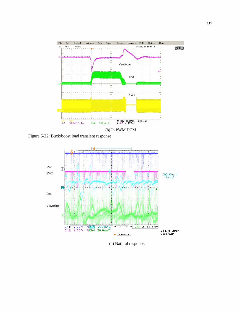
115
(b) In PWM DCM.
Figure 5-22: Buck/boost load transient response
(a) Natural response.
Vswitcher
Iind
SW1
SW1
SW2
Iind
Vswitcher
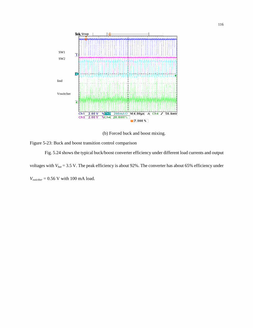
116
(b) Forced buck and boost mixing.
Figure 5-23: Buck and boost transition control comparison
Fig. 5.24 shows the typical buck/boost converter efficiency under different load currents and output
voltages with Vbat = 3.5 V. The peak efficiency is about 92%. The converter has about 65% efficiency under
Vswicther = 0.56 V with 100 mA load.
SW1
SW2
Iind
Vswitcher
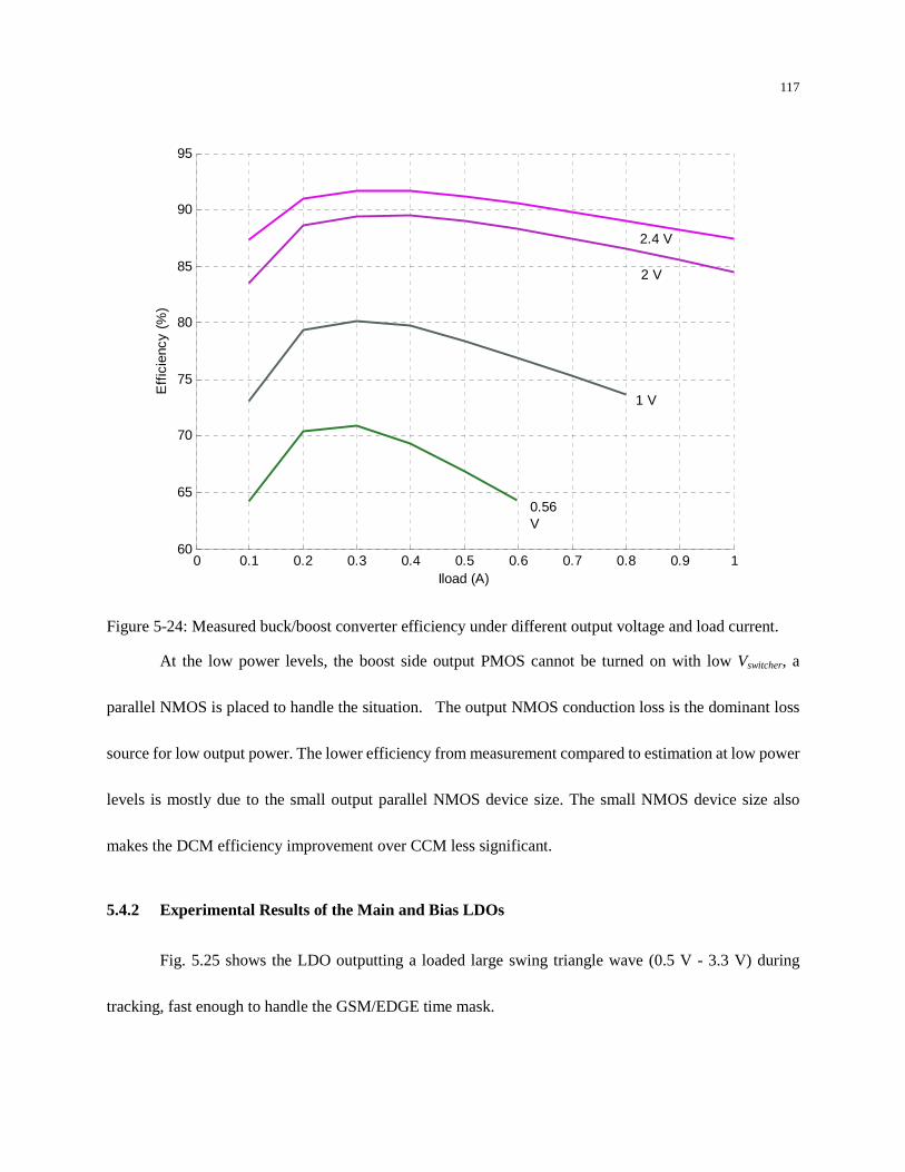
117
Figure 5-24: Measured buck/boost converter efficiency under different output voltage and load current.
At the low power levels, the boost side output PMOS cannot be turned on with low Vswitcher, a
parallel NMOS is placed to handle the situation. The output NMOS conduction loss is the dominant loss
source for low output power. The lower efficiency from measurement compared to estimation at low power
levels is mostly due to the small output parallel NMOS device size. The small NMOS device size also
makes the DCM efficiency improvement over CCM less significant.
5.4.2 Experimental Results of the Main and Bias LDOs
Fig. 5.25 shows the LDO outputting a loaded large swing triangle wave (0.5 V - 3.3 V) during
tracking, fast enough to handle the GSM/EDGE time mask.
0 0.1 0.2 0.3 0.4 0.5 0.6 0.7 0.8 0.9 160
65
70
75
80
85
90
95
Iload (A)
Eff
icie
ncy
(%)
1 V
2 V
0.56V
2.4 V
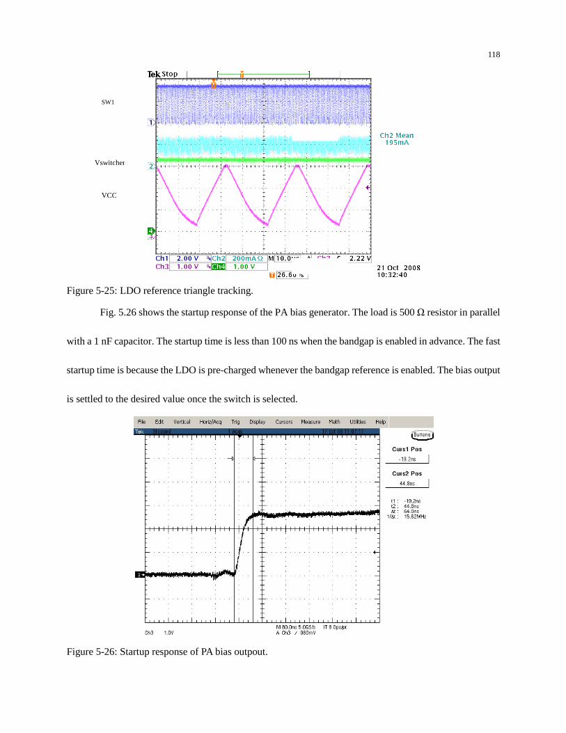
118
Figure 5-25: LDO reference triangle tracking.
Fig. 5.26 shows the startup response of the PA bias generator. The load is 500 Ω resistor in parallel
with a 1 nF capacitor. The startup time is less than 100 ns when the bandgap is enabled in advance. The fast
startup time is because the LDO is pre-charged whenever the bandgap reference is enabled. The bias output
is settled to the desired value once the switch is selected.
Figure 5-26: Startup response of PA bias outpout.
VCC
Vswitcher
SW1

119
5.4.3 Experimental Results for the Multi-Mode Supply with RF PA
This multi-mode supply has been evaluated with a multi-mode wideband PA sample board
(internal structure unknown) to check the system efficiency and linearity. Fig. 5.27 shows the total
efficiency of the PA with this multi-mode supply under different battery voltages and various operation
modes around 900 MHz. Under Vbat = 3.4 V, the PA output PAE is 57% with 33.5 dBm output power in
GSM, 36% with 28.5 dBm in linear EDGE, 38% with 28 dBm in voice WCDMA, 37% with 28 dBm in
HSDPA, 32% with 27 dBm in HSUPA, and 30% under 27 dBm in HSUPA with the 2.6 dB backoff. Under
these test conditions, the supply has been demonstrated no significant distortion added to the PA output for
the EDGE EVM and spectrum mask, and the WCDMA ACLR requirements.
The total efficiency of this multi-mode supply and the tested multi-mode PA is comparable to the
published efficiency data. The GSM/EDGE polar loop transmitter [2] reports 54% and 35% PAE with 33
dBm and 27 dBm output power in GSM and EDGE respectively. The polar EDGE transmitter with a buck
converter as the supply [7] reports much higher PAE 56% under much lower output power 20dBm. Paper
[11] reports PAE 56% in GSM and 29% in EDGE (similar efficiency achieved through power tracking or
envelope tracking) at full power.
The GSM receiver band noise has been evaluated. Fig. 5.28(a) and Fig. 5.28(b) show the noise
spectrum difference with and without the switching frequency dithering. It shows about 6 dB noise
reduction from the dithering inside the receiver band from the technique.
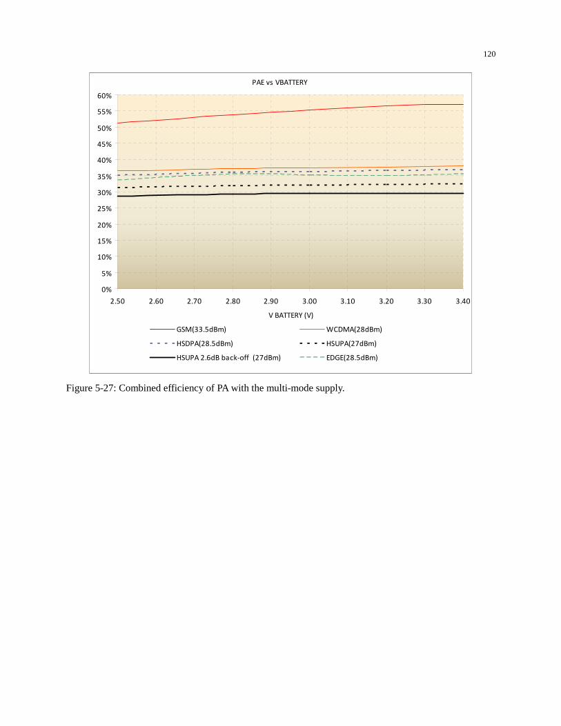
120
Figure 5-27: Combined efficiency of PA with the multi-mode supply.
PAE vs VBATTERY
0%
5%
10%
15%
20%
25%
30%
35%
40%
45%
50%
55%
60%
2.50 2.60 2.70 2.80 2.90 3.00 3.10 3.20 3.30 3.40
V BATTERY (V)
GSM(33.5dBm) WCDMA(28dBm)
HSDPA(28.5dBm) HSUPA(27dBm)
HSUPA 2.6dB back-off (27dBm) EDGE(28.5dBm)
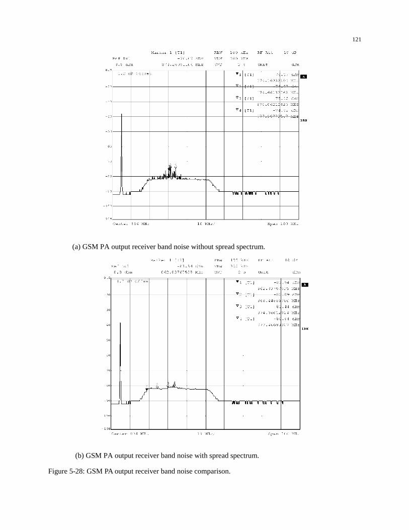
121
(a) GSM PA output receiver band noise without spread spectrum.
(b) GSM PA output receiver band noise with spread spectrum.
Figure 5-28: GSM PA output receiver band noise comparison.
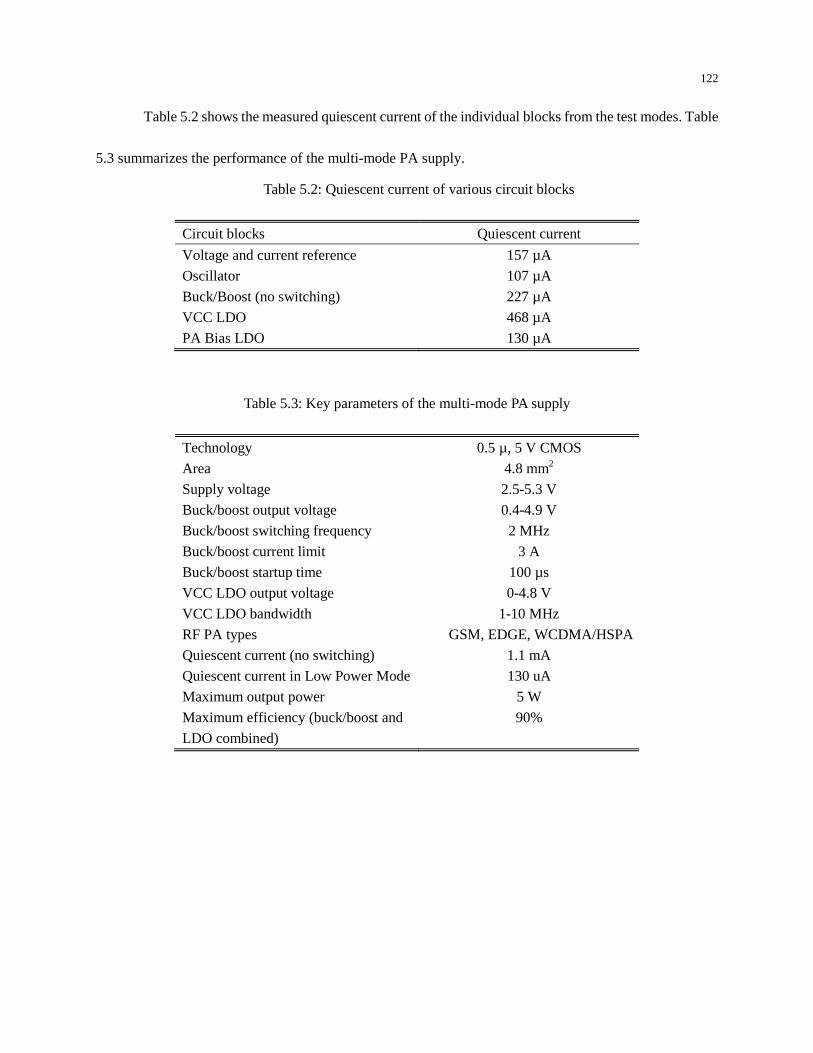
122
Table 5.2 shows the measured quiescent current of the individual blocks from the test modes. Table
5.3 summarizes the performance of the multi-mode PA supply.
Table 5.2: Quiescent current of various circuit blocks
Circuit blocks Quiescent current
Voltage and current reference 157 µA
Oscillator 107 µA
Buck/Boost (no switching) 227 µA
VCC LDO 468 µA
PA Bias LDO 130 µA
Table 5.3: Key parameters of the multi-mode PA supply
Technology 0.5 µ, 5 V CMOS
Area 4.8 mm2
Supply voltage 2.5-5.3 V
Buck/boost output voltage 0.4-4.9 V
Buck/boost switching frequency 2 MHz
Buck/boost current limit 3 A
Buck/boost startup time 100 µs
VCC LDO output voltage 0-4.8 V
VCC LDO bandwidth 1-10 MHz
RF PA types GSM, EDGE, WCDMA/HSPA
Quiescent current (no switching) 1.1 mA
Quiescent current in Low Power Mode 130 uA
Maximum output power 5 W
Maximum efficiency (buck/boost and
LDO combined)
90%

123
Chapter 6
Conclusions
6.1 Thesis Summary
The goal throughout this work has been to improve the RF transmitter efficiency with the focus on
the PA supply for the handset applications. The total efficiency is the product of the PA efficiency and its
supply efficiency. In Chapter 3, this dissertation has reviewed different PA supply architectures for high
efficiency, including average power tracking, envelope tracking and polar modulation. The architecture
choice is often related to the given PA design and the system requirements.
Although the simplest form of an efficient power tracking supply is a buck converter, a front-end
boost may be needed to maintain constant output power for low battery voltage conditions. When one
switching regulator drives another switching regulator, instability will occur because of the negative
incremental resistance of the constant power load of a high efficiency regulator. In Chapter 4, the peak and
valley current mode controls are modeled and analyzed in the presence of the constant power load, and it
is found that the current mode control inherently provides active damping, and effectively converts the
negative impedance of the CPL into a positive resistive load through the current feedback. The small-signal
response of a boost with CPL is extracted from the switching transient simulations and it has demonstrated
excellent matching with the model predicted results.
124
Transient response of a boost converter is often much slower than a buck converter with the same
passive components due to the presence of a RHP zero. Load current feedforward is an effective way to
improve the boost transient response. The small-signal response with the load current feedforward has been
analyzed. The control-to-output DC gain of a current-mode-controlled boost converter with CPL is constant,
independent of the power load levels. However the DC gain is varying like that of an equivalent resistive
load with a proper load current feedforward. The significance of this work is that the design of a boost
converter under CPL has been made as easy as the traditional design with a resistive load. The small-signal
modeling and analysis have been given as in the traditional design, and it is shown that the average model
can be used accordingly for the loop stability design and simulations.
In Chapter 5, this thesis explores the possibility of a practical integrated efficient power supply
driving the multi-standard RF PAs while meeting the specifications of the standards. There are significant
challenges from the time mask and receiver band noise requirements when applying a switching buck/boost
converter for the GSM/EDGE PAs. To address the switching noise issue, a spread spectrum technique has
been used and analyzed. To address the time mask issue, LAS architectures have been investigated.
Efficient architectures such as EER and ET do not distinguish the power control bandwidth and
the signal bandwidth. These architectures handle the power control dynamic range and the signal dynamic
range using the same wideband supply. Although the current mode parallel LAS architecture is suitable for
high power high PAR systems, the quiescent current required for wideband operation causes the
architecture to be inefficient under low power conditions. As WCDMA PDF has its maximum probability
around -2 dBm, the overall efficiency improvement from the current mode parallel LAS is limited.
The slow power control bandwidth and the fast signal bandwidth can be treated separately in the

125
series LAS architecture. The switcher handles the power control range, and a low quiescent current linear
LDO handles the signal bandwidth requirement. The series architecture is efficient for low PAR systems
because the LDO dropout between its input and output are set to as low as possible.
A buck/boost and LDO series architecture has been proposed and implemented as the multi-mode
RF PA supply. The circuit has been designed in a standard 0.5 µ, 5 V CMOS process. The test chip
measurement results have demonstrated the high efficiency in the GSM, EDGE and WCDMA/HSPA
operation modes.
The key contributions of this work include:
1) Modeling and analysis of boost converter with current model control under constant power
load (CPL)
• By modeling and analysis of both peak and valley current-model-control of a boost converter,
it has been shown that the current mode control is an effective way to address the stability
challenges related to CPL.
• It is shown that load current feedforward for a current-mode-controlled boost converter has
beneficial impact on transient responses.
2) Design of a high efficiency multi-mode PA supply based on the series linear-assisted-switcher
(LAS) architecture
• The challenges of operation over wide output voltage range have been addressed by
compensation that supports multiple operating modes, and by implementing a duty-cycle
dithering technique to suppress the sub-harmonic oscillation for the high buck and low boost
duty cycles.
126
• The wideband low-drop-out (LDO) linear regulator has been developed, with wide input and
output range using parallel output PMOS and NMOS devices. The two control loops share the
same error amplifier and are capable of smooth transition.
• High efficiency and wide bandwidth of the multi-mode PA supply were demonstrated from
the chip alone and when driving the PA.
• Switching frequency modulation effectiveness and importance were demonstrated
particularly in the boost mode. Analytic analysis for the noise reduction was performed.
6.2 Future Directions
In Chapter 3, to address the high PAR and wideband requirements in LTE and WiMAX systems, a
current mode ET LAS architecture, average power tracking for the Doherty amplifiers, and average power
tracking for the outphasing PAs have been proposed for further investigation. The last two architectures
again treat the power control and signal linearization separately. The wide power control range is handled
by a slow switcher, while the wideband signal linearity is handled by the Doherty or outphasing technique.
The linearization property from Doherty or outphasing technique needs to be maintained over the whole
power control dynamic range. In the Doherty case, a DSP is required for the adaptive base/gate biasing over
the power control range, though the bias adaption is very slow following the power control bandwidth.
Another area for further investigation is in the high power base-station applications. In Chapter 3, a
nested parallel LAS architecture is proposed to further improve the supply modulator efficiency by shifting
the medium-band power supplied from linear amplifier to a high switching frequency buck. A Class-H
rail-tracking linear amplifier is proposed for efficiency improvement. A more efficient supply modulator

127
will be able to make the base-station transmitter smaller and possibly mounted on the tower to save the
antenna cable loss as well.
128
References
[1] TQM7M5005 and TQM7M5012 datasheets, TriQuint Semiconductor.
[2] T. Sowlati, D. Rozenblit, E. MacCarthy, M. Damgaard, R. Pullela, D. Koh, and D. Ripley,
"Quad-band GSM/GPRS/EDGE polar loop transmitter," IEEE International Solid-State Circuits
Conference, Vol.1, Feb, 2004, pp. 186-521.
[3] M. R. Elliott, T. Montalvo, B. P. Jeffries, F. Murden, J. Strange, A. Hill, S. Nandipaku, and J.
Harrebek, "A polar modulator transmitter for GSM/EDGE," IEEE Journal of Solid-State Circuits,
vol. 39, pp. 2190-2199, Dec, 2004.
[4] X. Jiang, N. D. Lopez, and D. Maksimovic, "A switched mode envelope tracker for Polar EDGE
transmitter," 37th IEEE Power Electronics Specialists Conference, Jun., 2006, pp. 1-7.
[5] X. Jiang, Envelope-Tracking Power Supplies for RF Power Amplifiers in Portable Applications,
Ph.D. thesis, Department of Electrical and Computer Engineering, University of Colorado at
Boulder, 2007.
[6] N. Wang, X-band Class-E Power Amplifier with Dynamic Bias Control, Ph.D. thesis, Department
of Electrical and Computer Engineering, University of Colorado at Boulder, 2006.
[7] N. López, High-Efficiency Power Amplifiers for Linear Transmitters, Ph.D. thesis, Department
of Electrical and Computer Engineering, University of Colorado at Boulder, 2008.
[8] T. Kwak, M. Lee, and G. Cho, “A 2 W CMOS hybrid switching amplitude modulator for EDGE
polar transmitters,” IEEE J. Solid-State Circuit, vol. 42, no. 12, pp. 2666-2676, Dec. 2007.
[9] J. Popp, D. Y. C. Lie, F. Wang, D. Kimball, and L. Larson, "Fully-integrated highly-efficient RF
Class E SiGe power amplifier with an envelope-tracking technique for EDGE applications," 2006
IEEE Radio and Wireless Symposium, Jan, 2006, pp. 231-234.
[10] P. G. Blanken, R. Karadi, and H. J. Bergveld, “A 50 MHz bandwidth multi-mode PA supply
modulator for GSM, EDGE and UMTS application,” IEEE Radio Frequency Integrated Circuits
Symposium, pp. 401-404, June 2008.
[11] B. J. Minnis, P. A. Moore, P. N. Whatmouth, P. G. Blanken, and M. P. van der Heijden,
“System-efficiency analysis of power amplifier supply-tracking regimes in mobile transmitters,”
129
IEEE Tran. Circuits Systems I, Radio Frequency Integrated Circuits Symposium, vol. 56, no. 1,
pp. 268-279, Jan. 2009.
[12] J. Kitchen, C. Chu, S. Kiaei, and B. Bakkaloglu, “Combined linear and ∆-modulated
switched-mode PA supply modulator for polar transmitters,” IEEE J. Solid-State Circuit, vol.
44, no. 2, pp. 404-413, Feb. 2009.
[13] J. Park, J. Fan, K. G. Gard, and A. Huang, “10 MHz current mode 4 switch buck boost converter
(4SBBC) for polar modulation,”, IEEE Apec, Feb. 2008, pp. 1977-1983.
[14] J. Qin, R. Guo, J. Park, and A. Huang, “A low noise, high efficiency two stage envelope
modulator structure for EDGE polar modulation,”, in IEEE Int. Symp. Circuits Systems, May
2009, pp. 1089-1092.
[15] E. McCune, “High-efficiency, multi-mode, multi-band terminal power amplifiers,” IEEE
Microwave Magazine, Mar. 2005.
[16] K. Walsh, and J. Johnson, “3G/4G multimode cellular front end challenges,” RFMD white paper,
2009.
[17] “TRIUMF-next generation 3G converged RF architecture for mobile devices,” TriQuint
Semiconductor, 2009.
[18] RF6260 and RF6560, RFMD.
[19] 3GPP, TS 05.05, Technical Specification Group GSM/EDGE Radio Access Network, Radio
transmission and reception, V8.16.0, Release-1999, Aug, 2003.
[20] 3GPP, TS 25.101, Universal Mobile Telecommunications System (UMTS), User Equipment (UE)
radio transmission and reception (FDD), V8.6.0, Release 8, Mar., 2009.
[21] GSMA, Battery Life Measurement Technique, 5.1, Sept. 15, 2009.
[22] E. Spears, D. Teeter, D. Ngo and S. Martin, “Modulation trends and key specifications of mobile
transmitters,” IEEE RFIC Symp. Workshops, WSC, June 2006.
[23] S. C. Cripps, RF Power Amplifiers for Wireless Communication, Norwood, MA: Artech House,
1999.
[24] J. Hoversten, Efficiency and Linear Microwave Transmitters for High Peak-to-Average Ratio
Signals, Ph.D. thesis, Department of Electrical and Computer Engineering, University of
Colorado at Boulder, 2010.
130
[25] L. R. Kahn, "Single sideband transmission by envelope elimination and restoration," Proc. IRE,
July, 1952, pp. 803-806.
[26] F. H. Raab, "Intermodulation distortion in Kahn-technique transmitters," IEEE Transactions on
Microwave Theory and Techniques, vol. 44, pp. 2273-2278, Dec, 1996.
[27] B. Sahu and G. A. Rincon-Mora, "A high-efficiency WCDMA RF power amplifier with adaptive,
dual-mode buck-boost supply and bias-current control," IEEE Microwave Wireless Components
Letter, vol. 17, no. 3, pp. 238-240, May 2007.
[28] J. Deng, P.S. Gudem, L.E. Larson, D. Kimball and P.M. Asbeck, “A SiGe PA with dual dynamic
bias control and memoryless digital predistortion for WCDMA handset applications,” IEEE
Trans. on Microwave Theory and Techniques, vol. 41, no. 5, May 2006, pp. 1210 – 1221.
[29] J. Deng, P.S. Gudem, L.E. Larson, and P.M. Asbeck, “A high average-efficiency SiGe HBT
power amplifier for WCDMA handset applications,” IEEE Trans. on Microwave Theory and
Techniques, vol. 53, no. 2, Feb. 2005, pp. 529 – 537.
[30] J. Staudinger, B. Gilsdorf, D. Newman, G. Norris, G. Sadowniczak, R. Sherman, and T. Quach,
"High efficiency CDMA RF power amplifier using dynamic envelope tracking technique,"
IEEE MTT-S International Microwave Symposium Digest, vol. 2, June, 2000, pp. 873-876.
[31] G. Hanington, C. Pin-Fan, P. M. Asbeck, and L. E. Larson, "High-efficiency power amplifier
using dynamic power-supply voltage for CDMA applications," IEEE Transactions on Microwave
Theory and Techniques, vol. 47, pp. 1471-1476, Aug, 1999.
[32] T. Fowler, K. Berger, N. Cheng, A. Samelis, E. Enobakhare, and S. Rohlfing, “Efficiency
improvement techniques at low power level for linear CDMA and WCDMA power amplifiers,”
in Proc. IEEE RFIC Symp., pp. 41-44, 2002.
[33] L. Larson, P. Asbeck, and D. Kimball, "Next generation power amplifiers for wireless
communications - squeezing more bits out of fewer joules," in IEEE Radio Frequency integrated
Circuits (RFIC) Symposium, June, 2005, pp. 417-420.
[34] P. Asbeck, L. Larson, D. Kimball, Y. Zhao, F. Wang, and D. Qiao, “High dynamic range, high
efficiency power amplifiers for wireless communications,” in Proceedings of the
Bipolar/BiCMOS Circuits and Technology Meeting, 9-11 Oct. 2005, pp. 103 – 107.
[35] P. Asbeck, G. Hannington, P. F. Chen, and L. Larson, "Efficiency and linearity improvement in
power amplifiers for wireless communications," in 20th Annual Gallium Arsenide Integrated
Circuit (GaAs IC) Symposium, Nov, 1998, pp. 15-18.
[36] W. H. Doherty, “A new high efficiency power amplifier for modulated waves,” Proc. IRE, vol. 24,
no. 9, pp. 1163-1182, Sep. 1936.
131
[37] F. Raab, “Efficiency of outphasing RF power-amplifier systems,” IEEE Transactions on
Communications, vol. com-33, no. 10, pp. 1094-1099, Oct. 1985.
[38] R. Beltran, F. H. Raab, and A. Velazquez, “HF outphasing transmitter using Class-E power
amplifiers,” in IEEE MTT-S Int. Microwave Symp. Dig., vol. 33, no. 6, pp. 1094-1099, Jun. 2009.
[39] J. Grundlingh, K. parker, and G. Rabjohn, “A high efficiency Chireix out-phasing power
amplifier for 5GHz WLAN applications,” in IEEE MTT-S Int. Microwave Symp. Digest, vol. 3,
pp. 1535-1538, Jun. 2004.
[40] F. H. Raab, P. Asbeck, S. Cripps, P. B. Kenington, Z. B. Popovic, N. Pothecary, J. F. Sevic, and N.
O. Sokal, "Power amplifiers and transmitters for RF and microwave," IEEE Trans. Microwave
Theory Techniques, vol. 50, pp. 814-826, Mar. 2002.
[41] P. B. Kenington, M. Cope, R. M. Bennett, and J. Bishop, "A GSM-EDGE high power amplifier
utilising digital linearisation," in IEEE MTT-S International Microwave Symposium Digest, vol.3,
May, 2001, pp. 1517-1520.
[42] R. W. Erickson, and D. Maksimovic, Fundamentals of Power Electronics, 2nd ed., Springer, 2001.
[43] Y. Xiong, S. Sun, H. Jia, P. Shea, and Z.J. Shen, “New physical insights on power MOSFET
switching losses,” IEEE Trans. Power Electronics, vol. 24, no. 2, Feb. 2009, pp. 525 – 531.
[44] B. Schottstaedt, “An introduction to FM,” http://ccrma.stanford.edu/software/snd/snd/fm.html
[45] J. R. Carson, "Notes on the theory of modulation", Proc. IRE, vol. 10, no. 1, Feb. 1922, pp.
57-64.
[46] A. Santolaria, J. Balcells, D. Gonzalez, and J. Gago, “Evaluation of switching frequency
modulation in EMI emissions reduction applied to power converters,” Proc. IEEE IECON’03,
vol. 3, pp. 2306 – 2311, Nov. 2003.
[47] Y. Matsumoto, K. Fujii, and A. Sugiura, “Estimating the amplitude reduction of clock harmonics
due to frequency modulation,” IEEE Trans. Electromagnetic Compatibility, vol. 48, no. 4, pp.
734-741, Nov. 2006.
[48] V. Pinon, F. Hasbani, A. Giry, D. Pache, and C. Garnier, “A single-chip WCDMA envelope
reconstruction LDMOS PA with 130 MHz switched-mode power supply,” in IEEE ISSCC. Tech.
Dig., Feb. 2008, pp. 564-565.
[49] G. B. Yundt, “Series or parallel-connected composite amplifiers,” IEEE Trans. Power Electron.,
vol. PE-1, pp. 48-54, Jan. 1986.
[50] G. R. Walker, “A class B switch-mode assisted linear amplifier,” IEEE Trans. Power Electron. ,
132
vol.18, no.6, pp.1278-1285, Nov. 2003.
[51] A. E. Ginart, R. M. Bass and W. M. Leach Jr., T. G. Habetler, “Analysis of the class AD audio
amplifier including hysteresis effects,” IEEE Trans. Power Electron., vol. 18, no. 2, pp. 679-685,
Mar. 2003.
[52] R. A. R. van der Zee and E. van Tuijl, “A power-efficient audio amplifier combining switching
and linear techniques,” IEEE J. Solid-State Circuits, vol. 34, no. 7, pp. 985-991, Jul. 1999.
[53] N. S. Jung, N. I. Kim and G. H. Cho, “A new high-efficiency and super-fidelity analog amplifier
with the aid of digital switching amplifier,” in Proc.29th Annu. IEEE Power Electron. Spec. Conf.,
1998.
[54] H. Ertl, J. W. Kolar and F. C. Zach, “Basic considerations and topologies of switched-mode
assisted linear power amplifiers”, IEEE Trans. Ind, Electron., vol. 44, no. 1, pp. 116-123, Feb.
1997.
[55] V. Yousefzadeh, E. Alarcon, and D. Maksimovic, "Efficiency optimization in linear-assisted
switching power converters for envelope tracking in RF power amplifiers," IEEE International
Symposium on Circuits and Systems, vol. 2, May, 2005, pp. 1302-1305.
[56] Y. Li, and D. Maksimovic, “High efficiency wide bandwidth power supplies for GSM and EDGE
RF power amplifiers,”, IEEE Int. Symp. Circuits Systems, pp. 1314-1317, May 2005.
[57] F. Wang, D. Kimball, J. Popp, A. Yang, D. Y. C. Lie, P. Asbeck, and L. Larson, "Wideband
envelope elimination and restoration power amplifier with high efficiency wideband envelope
amplifier for WLAN 802.11g applications," IEEE MTT-S International Microwave Symposium
Digest, June, 2005, p. 4.
[58] N. Schlumpf, M. Declercq and C. Dehollain, “A fast modulator for dynamic supply linear RF
Power Amplifier,” IEEE J. Solid-State Circuit., vol. 39, no. 7, pp. 1015-1025, Jul. 2004.
[59] P. Midya, "Linear switcher combination with novel feedback," IEEE PESC 2000, vol. 3, pp.
1425-1429.
[60] W. Y. Chu, B. Bakkaloglu, and S. Kiaei, “A 10 MHz bandwidth, 2 mV ripple PA regulator for
CDMA transmitters,” IEEE J. Solid-State Circuit, vol. 43, no. 12, pp. 2809-2819, Dec. 2008.
[61] B. Kim, J. Choi, D. Kang, and D. Kim, “Envelope tracking technique for multimode PA
operation,” in Proc. 39th European Microwave Conf., pp. 429-432, Sept. 2009.
[62] D. Kang, D. Kim, J. Choi, J. Kim, Y. Cho, and B. Kim, “A multimode/multiband power amplifier
with a boosted supply modulator,” IEEE Trans. Microwave Theory Techniques, vol. 58, no.
10, Oct. 2010, pp. 2598-2608.
133
[63] LMH6678 datasheet, Texas Instruments.
[64] Y. Zhao, M. Iwamoto, L. E. Larson, P. M. Asbeck, “Doherty amplifier with DSP control to
improve performance in CDMA operation,” IEEE MTT-S International Microwave Symposium
Digest, vol. 2, Jun. 2003, pp. 687 – 690.
[65] D. Kimball, J. Jeong, C. Hsia, P. Draxler, S. Lanfranco, W. Nagy, K. Linthicum, L. E. Larson, and
P. M. Asbeck, “High-efficiency envelope-tracking W-CDMA base-station amplifier using GaN
HFETs,” IEEE Trans. Microwave Theory Techniques, vol. 54, no. 11, pp. 3848 – 3856, Nov.
2006.
[66] J. Jeong , D. Kimball, M. Kwak, P. Draxler, C. Hsia, C. Steinbeiser, T. Landon, O. Krutko, L. E.
Larson, and P. M. Asbeck, “High-efficiency WCDMA envelope tracking base-station amplifier
implemented with GaAs HVHBTs,” IEEE Journal Solid-State Circuit, vol. 44, no. 10, pp.
2629-2639, Oct. 2009.
[67] J. Choi, D. Kang, D. Kim, and B. Kim, “Optimized envelope tracking operation of Doherty
power amplifier for high efficiency over an extended dynamic range,” IEEE Tran Microwave
Theory Techniques, vol. 57, no. 6, pp. 1508-1515, Jun. 2009.
[68] C. Steinbeiser, T. Landon, C. Suckling, J. Nelson, J. Delaney, J. Hitt, L. Witkowski, G. Burgin, R.
Hajji, and O. Krutko, “250 W HVHBT Doherty with 57% WCDMA efficiency linearized to -55
dBc for 2c11 6.5 dB PAR,” IEEE J. Solid-State Circuit, vol. 43, no. 10, pp. 2218-2228, Oct.
2008.
[69] J. Pierdomenico, S. Wurcer, and B. Day, “A 684-mW adaptive supply full-rate ADSL CO driver,” ,
IEEE J. Solid-State Circuits, vol. 37, no. 12, Dec. 2002, pp. 1831 – 1838.
[70] A. M. Rahimi, and A. Emadi, “An analytic investigation of DC/DC power electronic converters
with constant power loads in vehicular power systems,” IEEE Trans. Power Electron., vol. 68, no.
6, pp. 2689-2702, July 2009.
[71] A. M. Rahimi, G. A. Williamson, and A. Emadi, “Loop-cancellation technique: a novel nonlinear
feedback to overcome the destabilizing effect of constant-power loads,” IEEE Trans. Vehicular
Technology, vol. 59, no. 2, pp. 650-661, Feb. 2010.
[72] M. Cespedes, L. Xing, and J. Sun, “Constant-power load system stabilization by passive
damping,” IEEE Trans. Power Electron. Letters, vol. 26, no. 7, Jul. 2011.
[73] D. J. Perreault, and G. Verghese, “Time-varying effects and average issues in models for
current-mode control,” IEEE Trans. Power Electron., vol. 12, no. 3, pp. 453-461, May 1997.
[74] R. D. Middlebrook, “Topics in multiple-loop regulators and current-mode programming,” IEEE
Trans. Power Electron., vol. PE-2, no. 2, pp. 109-124, Apr. 1987.
134
[75] R. B. Ridley, “A new, continuous-time model for current-mode control,” IEEE Trans. Power
Electron., vol. 6, no. 2, pp. 271-280, Apr. 1991.
[76] F. D. Tan, and R. D. Middlebrook, “A unified model for current-programmed converters,” IEEE
Trans. Power Electron., vol. 10, no. 4, pp. 397-408, Jul. 1995.
[77] R. B. Ridley, “A new continuous-time model for current-mode control with constant frequency,
constant on-time, and constant off-time, in CCM and DCM,” in IEEE Power Electron.
Specialists Conf., pp. 382-389, 1990.
[78] J.H. Lee, H.S. Bae, S.H. Park, and B.H. Cho, “Constant resistance control of solar array
regulator using average current model control,” in Proc. IEEE APEC, pp. 1544-1548, 2006.
[79] V. Grigore, J. Hatonen, J. Kyyra, and T. Suntio, “Dynamics of a buck converter with a constant
power load,” in IEEE Power Electron. Specialists Conf., vol. 1, pp. 72-78, 1998.
[80] L. R. Lewis, B. H. Cho, F. C. Lee, and B. A. Carpenter, “Modeling, analysis and design of
distributed power systems,” in Proc. IEEE Power Electronics Specialists’ Conf., pp. 152-159,
1989.
[81] B. Choi, B. H. Cho, and S. Hong, “Dynamics and control of DC-to-DC converters driving other
converters downstream,” IEEE Trans. Circuits Systems-I, vol. 46, no. 10, pp. 1240-1248, Oct.
1999.
[82] B. Johansson, “Analysis of DC-DC converters with current-mode control and
resistive load when using load current measurements for control,” in IEEE Power Electron.
Specialists Conf., pp. 165-172, 2002.
[83] R. Redl, and N. O. Sokal, “Near-optimum dynamic regulation of DC-DC converters using
feed-forward of output current and input voltage with current-mode control,” IEEE Trans.
Power Electron., vol. PE-1, no. 3, pp. 181-192, July 1986.
[84] H. Y. Cho, and E. Santi, “Peak-current-mode-controlled buck converter with positive
feedforward control,” in IEEE Energy Conversion Congress and Exposition, pp. 2928-2935,
009.
[85] M. Karppanen, M. Hankaniemi, T. Suntio, and M. Sippola, “Dynamical characterization of
peak-current-mode-controlled buck converter with output-current feedforward,” IEEE Trans.
Power Electron., vol. 22, no. 2, pp. 444-451, Mar. 2007.
[86] B. Bryant, and M.K. Kazimierczuk,“Voltage loop of boost PWM DC-DC converters with peak
current-mode control,” IEEE Trans. Circuits Systems-I, vol. 53, no. 1, pp. 99-105, Jan. 2006.
[87] http://www.simplistechnologies.com
135
[88] K. Kundert, “Simulation methods for RF integrated circuits,” in IEEE/ACM Int. Conf. CAD
Dig., pp. 752-765, 1997.
[89] A. Davoudi, J. Jatskevich, and P.L. Chapman, “Numerical dynamic characterization of peak
current-mode-controlled DC-DC converters,” IEEE Trans. Circuits Syst. II, vol. 56, no. 12, pp.
906-10, Dec. 2009.
[90] J. Chen, D. Maksimovic, and R.W. Erickson, “Analysis and design of a low-stress buck-boost
converter in universal-input PFC applications,” IEEE Trans. Power Electronics, vol. 21, no. 2,
Mar. 2006, pp. 320 – 329.
[91] R. Paul, and D. Maksimovic, “Smooth transition and ripple reduction in 4-switch non-inverting
buck-boost power converter for WCDMA RF power amplifier,” IEEE Int. Symp. Circuits Systems,
pp. 3266-3269, May 2008.
[92] L. Wai and S. R. Sanders, "An integrated controller for a high frequency buck converter," in 28th
Annual IEEE Power Electronics Specialists Conference, June, 1997, pp. 246-254.
[93] Z.-H. Shen, and H. Min, “Combination method of DC-DC converter and LDO to improve
efficiency and load regulation,” IET Electron. Lett., vol. 47, no. 10, pp. 615-617, May 2011.
[94] G. Nebel, T. Baglin, I. San Sebastian, H. Sedlak, and U. Weder, “A very low-drop voltage
regulator using NMOS output transistor,” in Proc. IEEE ISCAS 2005, Kobe, Japan, pp.
3857–3860, May 2005.
[95] P. Hasler, and A.C. Low, “Programmable low dropout voltage regulator,” in Proc. IEEE IWSOC
2005, Banff, Canada, pp. 459-462, July 2005.
[96] K. Salmi, C. Scarabello, O. Chevalerias, and F. Rodes, “4 V, 5 mA low drop-out regulator using
series-pass n-channel MOSFET,” IET Electron. Lett., vol. 35, no. 15 , pp. 1214-1215, 1999.
[97] Y. Li of Texas Instruments, “Efficient envelope tracking power supply for radio frequency or
other power amplifiers,” U.S. patent 8,098,093, issued Jan. 17, 2012.
[98] M. Norris, A Multi-Phase High Slew-Rate Tracking Supply for WCDMA/LTE Base Stations,
Ph.D. thesis, Department of Electrical and Computer Engineering, University of Colorado at
Boulder, 2012.
[99] C. Hsia, D.F. Kimball, S. Lanfranco, and P.M. Asbeck, “Wideband high efficiency
digitally-assisted envelope amplifier with dual switching stages for radio base-station envelope
tracking power amplifiers,” in Microwave Symposium Digest, IEEE MTT-S International, pp.
672-675, May 2010.
[100] Y. Li, K. Vannorsdel, A. Zirger, M. Norris, and D. Maksimovic, "Current Mode Control for

136
Boost Converters with Constant Power Load," IEEE Transactions On Circuits and Systems I:
Regular Papers, , vol. 59, no. 1, p. 198-206, Jan. 2012.
[101] M. Hassan, L. E. Larson, V. Leung, and P. M. Asbeck, “A combined series-parallel hybrid
envelope amplifier for envelope tracking mobile terminal RF power amplifier applications,”
IEEE J. Solid-State Circuit, vol. 47, no. 5, pp. 1185-1198, May 2012.

137
Appendix A
Bandgap Reference Cell Small-Signal and Process Variation
Analysis
The bandgap reference circuit is almost always used in the integrated power management ICs. Its
accuracy is very critical as it often affects the accuracy of other circuit parameters such as the output DC
accuracy of a DC/DC converter. In this appendix, the small signal and process variation of the bandgap
circuit are analyzed. Figure A-1 shows a basic CMOS bandgap reference cell. A startup circuit (not shown)
is required if the error amplifier is self-biased (generated by the bandgap reference cell itself). The DC
result can be easily obtained by forcing the error amplifier inputs equal potential.
( (-M X,X (« ln B X,XMC (-, 1 X,X(« ln B X,XMC (A.1)
where (® is the thermal voltage, and n is the size ratio of the 2 substrate PNPs.
138
Figure A-1: A bandgap reference.
A.1 Bandgap Reference Small-Signal Model
The bandgap reference circuit has special feedback feature that both the positive feedback and
negative feedback exist, though the net effect is the negative feedback in the steady state for the stable
operation. Figure A-2 shows the small signal model. The loop gain is
® ½ ¾ XM 1½MXM 1½M X, X 1½,BX 1½,C
X, X 1½,XM 1½M X, X 1½,1½M¿
½ XMXXM 1½M X, X 1½,
(A.2)
where ½, ½1 ln$X2X1%X3 and ½2 ½1 X1X2 are transconductance of PMOS, Q1 and Q2 respectively.
139
Figure A-2: Small-signal model of the bandgap reference.
A.2 Bandgap Reference Process Variation
The process, temperature and supply variations can affect the reference accuracy. The process
variation is often the most significant contributor. The process variations include the threshold and
geometry mismatching of PMOS and NMOS differential pair or current mirrors, the resistors mismatching,
the Vbe variation, and the PNP Vbe mismatching. In the following, the impact on the reference accuracy
from the mismatches will be analyzed.
The error amplifier offset is often the most significant error source. Fig. A.3(a) shows the small
signal model with the error amplifier offset Vos. The Vbg error ³ can be found from the following:
140
½ ¾ XM 1½MXM 1½M X, X 1½,BX 1½,C (9
X, X 1½,XM 1½M X, X 1½,1½M ¿
= ½ h f°f´f°R °ªO°Rf Rf´R °ªO (9i ® ½(9
À ½(91 ® (9 XM 1½M X, X 1½,XMX
À ³ BXM 1½MC BX, X 1½,CXM 1½M X, X 1½,
(9 BXM 1½MC BX, X 1½,CXMX
(A.3)
i
bgv
Figure A-3: Small-signal model of the bandgap reference with amplifier offset.
The resistors mismatching caused Vbg error ³can also be calculated from the small signal model.
Fig. A.3(b) shows the small signal model with the error current - caused by a resistor mismatching. For
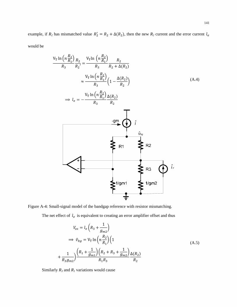
141
example, if R2 has mismatched value X,Á X, ∆X,, then the new R2 current and the error current -
would be
VÄ ln $ X,XM%XX,X,Å VÄln $ X,XM%X
X,X, ∆X, VÄ ln $ X,XM%X B1 ∆X,X, C
À - VÄ ln $ X,XM%X∆X,X,
(A.4)
i
bgv
ei
Figure A-4: Small-signal model of the bandgap reference with resistor mismatching.
The net effect of - is equivalent to creating an error amplifier offset and thus
(9 - BX 1½,C
À ³ VÄ ln B X,XMC B1 1X½,C BXM 1½MC BX, X 1½,CXMX
∆X,X,
(A.5)
Similarly R3 and R1 variations would cause
142
³ VÄ ln B X,XMC B 1X½,C BXM 1½MC BX, X 1½,CXMX∆XX (A.6)
³ VÄ ln B X,XMC 1X½,BXM 1½MC BX, X 1½,CXMX
∆XMXM (A.7)
The total Vbg variation can be further calculated statistically based on the independent individual
variations.
³, (9, ¾Æ1 XXM ln $ X,XM%Ç Æ1 X,X X,XM ln $ X,XM%Ç¿,
¾VÄ Æ1 XXM ln $ X,XM%Ç Æ1 X,X
X,XM ln $ X,XM%È¿,
VAln B X,XMC X,XMD, B∆X,X, C,
BX,XMC, ÉB∆XMXM C, B∆XX C,Ê[
(A.8)
The error amplifier input referred offset Vos can be derived from a given amplifier. For example in
Fig. A.5, Vos of the folded cascade amplifier can be calculated based on the square law relationship between
the Ids and Vgs of a MOS transistor.
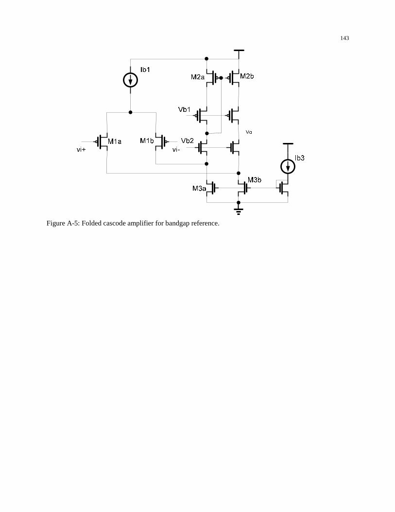
143
Figure A-5: Folded cascode amplifier for bandgap reference.
144
(9, ËÌÌÍP∆(,;MQ, B(9M (,;M2 C, Æ∆ ÎMnMÎMnM
Ç,
ÏÐÐÑ
B½,½MC,ËÌÌÍP∆(,;,Q, B(9, (,;,2 C, Æ ∆ Î,n,Î,n,
Ç,
ÏÐÐÑ
B½½MC,ËÌÌÍP∆(,Q, B(9 (,2 C, Æ∆ ÎnÎn
Ç,
ÏÐÐÑ
ËÌÌÍP∆(,;MQ, )M2Ò;8 ÎMnM
Æ∆ ÎMnMÎMnMÇ
,
ÏÐÐÑ
Î,n, ) )MÎMnM )M ËÌÌÍP∆(,;,Q, ) )M2Ò;8 Î,n,
Æ∆ Î,n,Î,n,Ç
,
ÏÐÐÑ
Ò În )Ò; ÎMnM )M ËÌÌÍP∆(,Q, )2Ò8 În
Æ∆ ÎnÎnÇ
,
ÏÐÐÑ
(A.9)
where the Wi and Li are referring the i-th transistor width and length, gmi is the i-th transistor
trans-conductance, Ib1 and Ib3 are the bias currents, and ∆(,;M , ∆(,;, and ∆(,are their threshold
mismatching.
Different type of bandgap reference cells may be calculated similarly. For example, Fig. A.6 shows
a different construction. Though it has less resistor mismatching than that of Fig. A.1 due to the elimination
of R1, the accuracy of this reference would be much worse than that of Fig. A.1 if the two designs are scaled
the same way. This is because the resistor mismatching is negligible compared against a MOS current
mirror mismatching with similar area in a typical CMOS process. The total Vbg variation of this reference
cell can be calculated similarly and is given below.
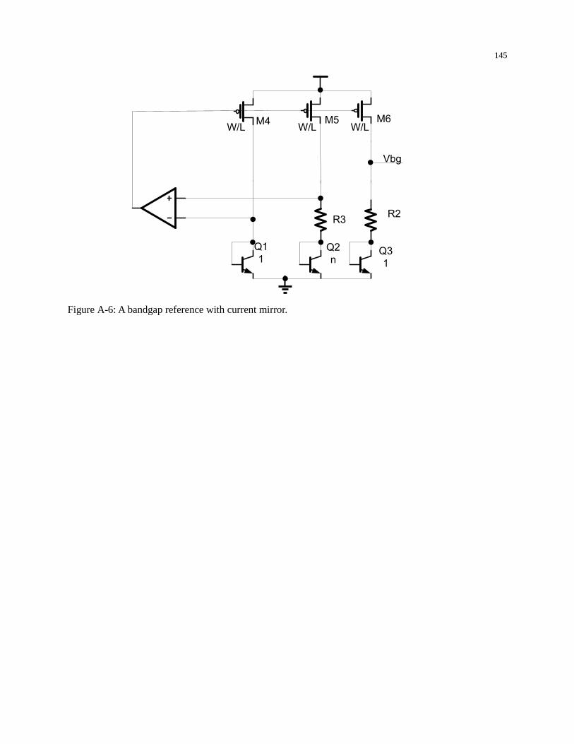
145
Q1
1Q2
n
R2R3
Vbg
Q3
1
M4 M5 M6W/L W/L W/L
Figure A-6: A bandgap reference with current mirror.
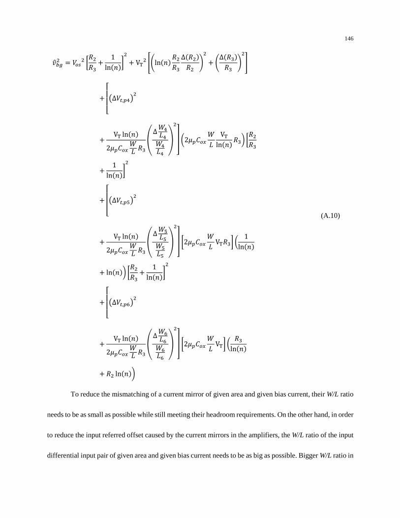
146
³, (9, AX,X 1lnD, VÄ, Óhln X,X∆X,X, i, h∆XX i,Ô
ËÌÌÍP∆(,;?Q,
VÄ ln2Ò;8 În X Æ∆ Î?n?Î?n?Ç
,¿ B2Ò;8 În VÄln XC AX,X 1lnD,
ËÌÌÍP∆(,;Q,
VÄ ln2Ò;8 În X Æ∆ ÎnÎnÇ
,¿ A2Ò;8 În VÄXD B 1ln lnC AX,X 1lnD,
ËÌÌÍP∆(,;ÕQ,
VÄ ln2Ò;8 În X Æ∆ ÎÕnÕÎÕnÕÇ
,¿ A2Ò;8 În VÄD B Xln X, lnC
(A.10)
To reduce the mismatching of a current mirror of given area and given bias current, their W/L ratio
needs to be as small as possible while still meeting their headroom requirements. On the other hand, in order
to reduce the input referred offset caused by the current mirrors in the amplifiers, the W/L ratio of the input
differential input pair of given area and given bias current needs to be as big as possible. Bigger W/L ratio in

147
the input differential pair causes bigger Gm, and smaller W/L ratio in the current mirrors causes the higher
output impedance, so they should be part of the loop gain bandwidth and stability design as well.