Embed Size (px)
Citation preview
HAL Id: tel-01399630https://tel.archives-ouvertes.fr/tel-01399630
Submitted on 20 Nov 2016
HAL is a multi-disciplinary open accessarchive for the deposit and dissemination of sci-entific research documents, whether they are pub-lished or not. The documents may come fromteaching and research institutions in France orabroad, or from public or private research centers.
L’archive ouverte pluridisciplinaire HAL, estdestinée au dépôt et à la diffusion de documentsscientifiques de niveau recherche, publiés ou non,émanant des établissements d’enseignement et derecherche français ou étrangers, des laboratoirespublics ou privés.
High efficiency reconfigurable RF power amplifiers inSOI CMOS technology for multi standard applications
Gauthier Tant
To cite this version:Gauthier Tant. High efficiency reconfigurable RF power amplifiers in SOI CMOS technology for multistandard applications. Micro and nanotechnologies/Microelectronics. Université Grenoble Alpes,2015. English. NNT : 2015GREAT101. tel-01399630

THÈSE Pour obtenir le grade de
DOCTEUR DE L’UNIVERSITÉ GRENOBLE ALPES Spécialité : Nano Electronique Nano Technologies
Arrêté ministériel : 7 août 2006
Présentée par
Gauthier TANT
Thèse dirigée par Jean-Michel FOURNIER, Jean-Daniel ARNOULD et
codirigée par Alexandre GIRY
préparée au sein du CEA LETI Grenoble en collaboration avec l’IMEP LAHC dans l'École Doctorale Electronique, Electrotechnique, Automatique et Traitement du Signal (EEATS)
Etude et intégration en SOI d’amplificateurs de puissance reconfigurables pour applications multi-modes multi-bandes
Thèse soutenue publiquement le19 novembre 2015,
devant le jury composé de :
Monsieur Tuami LASRI Professeur à l’Université de Lille 1, Président du jury
Monsieur Thierry PARRA Professeur à l’Université Paul Sabatier à Toulouse, Rapporteur
Monsieur Thierry TARIS Professeur à l’INP Bordeaux, Rapporteur
Monsieur Jean-Michel FOURNIER Professeur à Grenoble INP, Directeur de thèse
Monsieur Jean-Daniel ARNOULD Maître de Conférences à Grenoble INP, Co-directeur de thèse
Monsieur Alexandre GIRY Ingénieur de recherche au CEA LETI à Grenoble, Co-encadrant
Monsieur Pierre VINCENT Chef de service au CEA LETI à Grenoble, Invité
Monsieur Jean-Christophe NANAN Chef d’équipe design NPI chez Freescale France à Toulouse, Invité

2

3
Acknowledgement After four years working towards the Ph. D. degree at CEA LETI in collaboration with IMEP-
LAHC in Grenoble, thanks are in order for many people. First I would like to thank Pierre VINCENT, head of the Integrated RF Architectures Laboratory (LAIR) for welcoming me in his team, providing me with the means and tools to work in the best conditions and for accepting to come to the defense.
I would also like to respectfully thank my supervisor and co-supervisor from Grenoble INP – PHELMA, Jean-Michel FOURNIER and Jean-Daniel ARNOULD, who I know from my second year of engineering school, for accepting to accompany me during this adventure. I am also most thankful for their trust, advices, support and sometimes wake-up calls which led to this manuscript.
I, for one, know that without the guidance, help and understanding of Alexandre GIRY, none of this would have been possible. Alex, there is no word to express my gratefulness for these four years. We had a rough time during the writing of this thesis, but finally and thanks to you sharp eye, this work is achieved. I am proud that you entrusted me with this research work and to call you friend. I hope you stay the way you are and keep training young researchers in the field of power amplifiers like you trained me.
Special thanks also to Thierry PARRA, from Université Paul Sabatier in Toulouse, and Thierry TARIS, from INP Bordeaux, for giving me the honor to review my Ph. D. work. Many thanks also to Tuami LASRI from Université de Lille 1 for presiding over the jury.
A. Many thanks also to Jean-Christophe NANAN, my manager at Freescale France SAS in
Toulouse for accepting to come to my defense soon after hiring me. I hope the work you
saw was interesting and comforts you in your choice of including me in your team.
I would also like to thank Gabriel PARES, from the 3D integration team in CEA-LETI for his support during the TSV processing of the devices and Yves GAMBERINI for demonstrator assembly.
Adequate thanking process is in order for many other friends:
Glandito (Paco), Flaskito (Olivier), Clemencito (Clément), and The Last of the
Mexicans (Farid), jewel of the young researchers at CEA LETI (at least before their
post-doc) and above all friends on whom you can count. Thank you to the
“expendables” of the “thésard” box
The relief of the PA team in the LAIR: Dominique and Pierre. Thank you for your
friendship. Now it is your turn to shine and show everyone that PA design is fun. I
hope to see you both soon.
Thanks to all the Ph. D. students and colleagues with whom we had a lot of
interesting discussions, in particular Vitor, Zyad, Fred, Alexandra from IMEP LAHC
and Matthieu, Robert, Guillaume, Alin, Amine, Nelvin, Anthony and “Jesus” from
CEA LETI
“Old” friends from PHELMA, Mayu, Carole, Yves, Vincent, Cyrille, Aude, Quentin,
Quentin (yes that is right, there are two of them). Thank you all for understanding
the pressure of the thesis and not blaming me for not hanging out every time. But
do not worry; now I am free to have a beer with you anytime we meet and have a
good dinner in a Tex-Mex restaurant near Victor Hugo…
Thanks also to all the other I may have forgotten…

Acknowledgement
4
Pap, Mam, Sylvain, Alex, my parents and brothers, you deserve also your share of thank for your unfailing support and never let me down even in the worst times.
Last but not least, thank you my wife, Xuesong, for your support, understanding and most of all your love during these busy years. Now, all that is certain is that:
“It always seems impossible until it’s done”
Nelson MANDELA
5
Contents Acknowledgement ............................................................................................................................. 3
Contents ............................................................................................................................................. 5
Introduction ....................................................................................................................................... 9
Chapter I: Context ...................................................................................................................... 11
I-1 Introduction ...................................................................................................................... 11
I-2 Cellular telecommunications evolution ............................................................................ 11
I-2.1. 2Gstandards ............................................................................................................... 11
I-2.2. 3G standards .............................................................................................................. 12
I-2.3. 4G standards .............................................................................................................. 12
I-3 Cellular RF Front End ......................................................................................................... 13
I-3.1. RF Front End Module (FEM) ....................................................................................... 13
I-3.2. RF Power Amplifier Module (PAM) ............................................................................ 15
I-4 SOI CMOS technology overview........................................................................................ 26
I-4.1. RF devices ................................................................................................................... 27
I-4.2. Through Silicon Via ..................................................................................................... 29
I-5 Conclusion ......................................................................................................................... 30
I-6 References ........................................................................................................................ 31
Chapter II: Power Amplifier Design............................................................................................. 35
1 Introduction .......................................................................................................................... 35
II-1 Power amplifier characteristics ........................................................................................ 36
II-1.1. Power gain ................................................................................................................. 36
II-1.2. Efficiency .................................................................................................................... 37
II-1.3. Linearity...................................................................................................................... 38
II-2 Power stage design ........................................................................................................... 42
II-2.1. LDMOS transistor model ............................................................................................ 43
II-2.2. Design parameters ..................................................................................................... 43
II-2.3. Classes of operation ................................................................................................... 45
II-2.4. Saturated PA .............................................................................................................. 52
II-2.5. Linear PA .................................................................................................................... 56
II-3 Output matching network design ..................................................................................... 59
II-4 Tunable capacitor design .................................................................................................. 60

Contents
6
II-4.1. Switched capacitor bank ............................................................................................ 62
II-5 RF switch design ................................................................................................................ 64
II-5.1. SP1T ............................................................................................................................ 65
II-5.2. SPnT ............................................................................................................................ 66
II-6 Conclusion ......................................................................................................................... 67
II-7 References ........................................................................................................................ 68
Chapter III: Reconfigurable Multi-Mode Multi-Band Power Amplifier Design ............................ 69
III-1 Introduction ...................................................................................................................... 69
III-2 Reconfigurable MMPA architecture ................................................................................. 70
III-3 Reconfigurable MMPA design ........................................................................................... 71
III-3.1. Reconfigurable power stage design ........................................................................... 71
III-3.2. Reconfigurable output matching network design ..................................................... 76
III-3.3. Driver stage design ..................................................................................................... 87
III-3.4. Input matching network design ................................................................................. 89
III-3.5. Inter-stage matching network design ........................................................................ 90
III-3.6. Reconfigurable MMPA line-up implementation ........................................................ 93
III-4 Measured performances ................................................................................................... 94
III-4.1. Power amplifier characterization ............................................................................... 95
III-4.2. Output matching network characterization .............................................................. 97
III-4.3. MMPA line-up characterization ................................................................................. 99
III-5 Conclusion ....................................................................................................................... 100
III-6 References ...................................................................................................................... 101
Chapter IV: Study of High Efficiency PA architectures ............................................................... 103
IV-1 Introduction .................................................................................................................... 103
IV-2 PA efficiency enhancement ............................................................................................ 103
IV-2.1. Efficiency enhancement limitations ......................................................................... 104
IV-3 Supply and load modulation PA design .......................................................................... 105
IV-3.1. Envelope Tracking .................................................................................................... 105
IV-3.2. Load Modulation ...................................................................................................... 108
IV-4 Design and implementation of a load modulated PA architecture ................................ 110
IV-5 Conclusion ....................................................................................................................... 119
IV-6 References ...................................................................................................................... 120
Conclusion and perspective ........................................................................................................... 121
Published work .............................................................................................................................. 123

Contents
7
International conferences .......................................................................................................... 123
National conferences ................................................................................................................. 123
Appendices .................................................................................................................................... 125
Appendix A: Fourier Coefficient Calculations ............................................................................ 125
Appendix B: Current and voltage coefficients calculation in non-sinusoidal classes ................ 136
Appendix C: Determination of the input impedance of a transistor according to the
degeneration inductance ................................................................................................................ 138
Appendix D: Calculation of the required transistor width in a switched capacitor branch ...... 141
Appendix E: Determination of the capacitance of a second harmonic trap not interfering with
the fundamental impedance .......................................................................................................... 142
Appendix F: Calculation of the trap capacitor according to the trap inductance and parallel
impedance ...................................................................................................................................... 143
Appendix G: Calculation of the minimum Q-factor of a binary weighted switched capacitor
bank................................................................................................................................................. 144
Figure index.................................................................................................................................... 147
Table index ..................................................................................................................................... 153
List of acronyms and abbreviations ............................................................................................... 155
Abstract .......................................................................................................................................... 157
Résumé .......................................................................................................................................... 158

Contents
8

9
Introduction During the last two decades, the cellular telecommunications have been expanding
exponentially. This expansion has mainly been driven by the consumer needs for more diverse services. Each service addition was carried by a new standard generation. Furthermore, the obsolescence of old radio services, such as Terrestrial Analog Television, has released frequency bands that have been recently reallocated to cellular applications.
Following these trends, cellular devices are becoming more and more complex. The Front-End Module (FEM), which is the interface between the RF transceiver and the antenna, has to cope with the new standards (4G) while maintaining the compatibility with the former ones (2G, 3G). Inside the Front-End Module, the Power Amplifier (PA) is a major contributor to the performance of the FEM, but also to its complexity and energy consumption. Nowadays, a FEM can be required to address more than 10 frequency bands among all the current standards, often meaning numerous PA. Furthermore, the PA is required to be highly energy efficient.
Reducing the complexity and consumption of FEM can be done by using new PA architectures. Those architectures should handle several standards and bands using a limited number of PA with maximal efficiency in every operating mode. Reconfigurable PA seems to be promising for coping with these constraints and they are currently a major research subject.
While the traditional GaAs based technologies offer high PA performances, SOI CMOS technology offers a promising path for further integration of reconfigurable PA at reduced cost.
This thesis focuses on study and integration of a reconfigurable multi-mode multi-band power amplifier (MMPA) in SOI CMOS 130nm technology. The original solution proposed in this work represents a significant step toward the integration of high efficiency MMPA for cellular handset applications. This manuscript is divided in four chapters.
The First Chapter begins with a presentation of the context of this work. Issues associated with MMPA and performances of traditional MMPA architectures are introduced. The SOI CMOS technology used in this work for MMPA integration is also presented with a focus on the available power devices and passive elements.
In the Second Chapter, PA performances are first defined. A design methodology for saturated and linear PA integration is then proposed. Matching networks are critical for optimal PA operation. In order to realize tunable matching networks, tunable capacitors and mode switches are required. The design methodology of such devices is presented while ensuring the performance of the full architecture.
The Third Chapter focuses on the design of a new reconfigurable MMPA architecture and its integration in SOI CMOS.A focus is made on a reconfigurable power device and its implementation. Reconfigurability presents serious challenges for the design of PA the line-up and to ensure correct performance of the proposed architecture the required tradeoffs are presented. Then, implementation and measurement results of the developed SOI CMOS MMPA are presented and compared to state of the art.
The last Chapter presents a comparative study of two different high efficiency PA architectures based on supply and load modulation. The goal of this study is to determine the applications for which each technique is advantageous, both in terms of efficiency and linearity. Lastly, the design and SOI CMOS implementation of passive load modulation PA architecture is proposed. This demonstrator targets watt-level output power with high back-off efficiency improvement for cellular femto cell applications.

Introduction
10
11
Chapter I: Context
I-1 Introduction
The first part of this chapter will present a brief history of cellular telecommunications from the second generation (2G) up to the current fourth generation (4G). The front-end module constraints associated with each standard will be given.
The second part will present the Front-End module with a focus on the power amplifier. Three power amplifier architectures, from the simplest Mode Specific architecture to the more advanced Converged architecture, will be presented. Afterwards, reconfigurable power amplifiers will be introduced.
The last part gives an overview of the SOI-CMOS 130 nm technology (STMicroelectronics) which has been chosen for the implementation of the designed circuits.
I-2 Cellular telecommunications evolution
Since the first deployment of cellular networks in the 80s, a lot of changes have been introduced in the cellular world. This first part will give information on the gradual transformation of mobile telecommunication standards with a focus on European Standards.
I-2.1. 2Gstandards
During the ‘90s, the cellular telecommunication market exploded. The users from the first generation (1G) analog standard rapidly saturated the cellular networks and the analog encoding was showing its limits in terms of data rate and security. At that time, two standards were studied: The Interim Standard 95 (IS-95, also called CDMA-One) developed by Qualcomm in the USA in the 900MHz and 1950MHz AMPS bands, and the Global System for Mobile Communications (GSM) introduced by the European Telecommunication Standardization Institute (ETSI) for the 835 MHZ and 1800MHz TACS bands.
The first breakthrough compared to the first generation was the use of more robust digital encoding compared to 1G. In the GSM standard, frequency duplex is used to differentiate between uplink and downlink transmission and Time Division Multiple Access (TDMA) is used to share each channel between 8 users. IS-95 takes advantage of Code Division Multiple Access (CDMA) to differentiate uplink and downlink communication and to share each channel between users. GSM is the most widespread 2G standard while IS-95 and its evolutions are only located in Northern America.
In the late 90’s GSM was improved to General Packet Radio Service (GPRS), which allowed taking advantage of unused slots in order to improve the data rates. Later, in 2003, the Enhanced Data-rate for GSM Evolution (EDGE) was deployed. Using a new modulation scheme, its data rate is further improved.
Table 1: Characteristics of TX signals for GSM handsets.
Standard Output Power @ antenna Modulation
GSM (Low Band) 33dBm GMSK (Constant Envelope)
GSM (High Band) 30dBm
2G standards are still used nowadays for their robustness and capability to maintain communication on long ranges. However the evolution towards higher data rates has been allowed thanks to the introduction of 3G standard.
Chapter 1: Context
12
I-2.2. 3G standards
With the users starting to use their equipment in everyday life, more and more services were developed, especially media streaming and faster internet connections. In the beginning of the 21st century, Japan launched the first 3G standard: Wideband Code Division Multiple Access (W-CDMA). In the US, the evolution favored the CDMA 2000 standard, as an evolution of IS-95. The first major change with 3G was the allocation of new bands (around 2GHz). In the case of WCDMA, those bands were split in 5MHz channels and more complex Quadrature Amplitude Modulations (QAM) were introduced. By further improving controls, High Speed Packet Access (HSPA) was developed to improve data rates. Evolved HSPA (HSPA+) unlocked even higher data rates with QAM 64 and the introduction of Multiple Input Multiple Output (MIMO) systems.
Table 2: Characteristics of TX signal for 3G handsets.
Standard Output Power @ antenna Modulation PAPR
W-CDMA Release’99 24dBm
HPSK (Amplitude & phase) 3.5dB
HSUPA QAM (Amplitude & phase) 6.6dB
Today 3G is widely deployed around the world in urban areas where most of the population is concentrated. Following on its momentum, the search of even higher data-rates continued with the introduction of 4G standard.
I-2.3. 4G standards
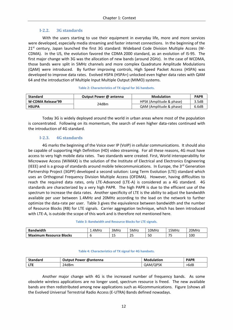
4G marks the beginning of the Voice over IP (VoIP) in cellular communications. It should also be capable of supporting High Definition (HD) video streaming. For all these reasons, 4G must have access to very high mobile data rates. Two standards were created. First, World interoperability for Microwave Access (WiMAX) is the solution of the Institute of Electrical and Electronics Engineering (IEEE) and is a group of standards around mobile telecommunications. In Europe, the 3rd Generation Partnership Project (3GPP) developed a second solution: Long Term Evolution (LTE) standard which uses an Orthogonal Frequency Division Multiple Access (OFDMA). However, having difficulties to reach the required data rates, only LTE-Advanced (LTE-A) is considered as a 4G standard. 4G standards are characterized by a very high PAPR. The high PAPR is due to the efficient use of the spectrum to increase the data rates. Another specificity of LTE is the ability to adjust the bandwidth available per user between 1.4MHz and 20MHz according to the load on the network to further optimize the data-rate per user. Table 3 gives the equivalence between bandwidth and the number of Resource Blocks (RB) for LTE signals. Carrier aggregation technique, which has been introduced with LTE-A, is outside the scope of this work and is therefore not mentioned here.
Table 3: Bandwidth and Resource Blocks for LTE signals.
Bandwidth 1.4MHz 3MHz 5MHz 10MHz 15MHz 20MHz
Maximum Resource Blocks 6 15 25 50 75 100
Table 4: Characteristics of TX signal for 4G handsets.
Standard Output Power @antenna Modulation PAPR
LTE 24dBm QAM/QPSK >6dB
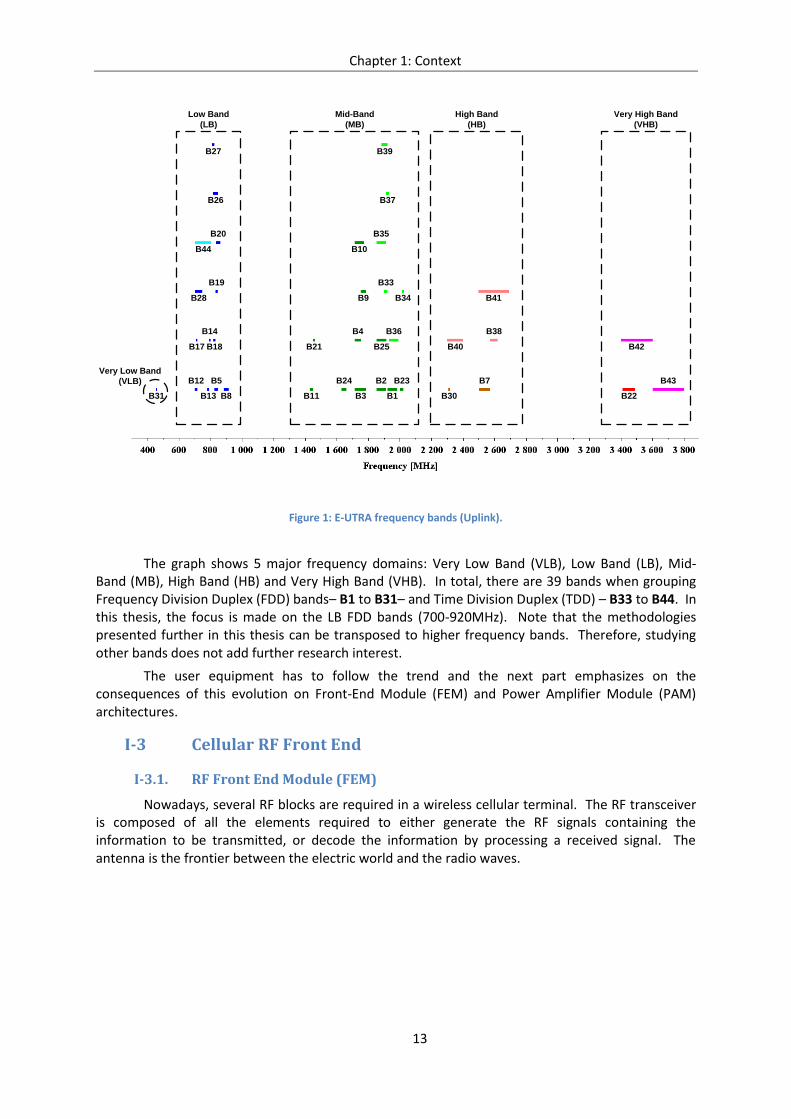
Another major change with 4G is the increased number of frequency bands. As some obsolete wireless applications are no longer used, spectrum resource is freed. The new available bands are then redistributed among new applications such as 4Gcommunications. Figure 1shows all the Evolved Universal Terrestrial Radio Access (E-UTRA) Bands defined nowadays.
Chapter 1: Context
13
Figure 1: E-UTRA frequency bands (Uplink).
The graph shows 5 major frequency domains: Very Low Band (VLB), Low Band (LB), Mid-Band (MB), High Band (HB) and Very High Band (VHB). In total, there are 39 bands when grouping Frequency Division Duplex (FDD) bands– B1 to B31– and Time Division Duplex (TDD) – B33 to B44. In this thesis, the focus is made on the LB FDD bands (700-920MHz). Note that the methodologies presented further in this thesis can be transposed to higher frequency bands. Therefore, studying other bands does not add further research interest.
The user equipment has to follow the trend and the next part emphasizes on the consequences of this evolution on Front-End Module (FEM) and Power Amplifier Module (PAM) architectures.
I-3 Cellular RF Front End
I-3.1. RF Front End Module (FEM)
Nowadays, several RF blocks are required in a wireless cellular terminal. The RF transceiver is composed of all the elements required to either generate the RF signals containing the information to be transmitted, or decode the information by processing a received signal. The antenna is the frontier between the electric world and the radio waves.
B1
B2
B3
B4
B5 B7
B8
B9
B10
B11
B12
B13
B17 B18
B19
B20
B21
B22
B23B24
B25
B26
B27
B28
B30B31
B33
B34
B35
B36
B37
B38
B39
B40
B41
B42
B43
B44
B14
Low Band
(LB)
Mid-Band
(MB)
High Band
(HB)
Very High Band
(VHB)
Very Low Band
(VLB)
Chapter 1: Context
14
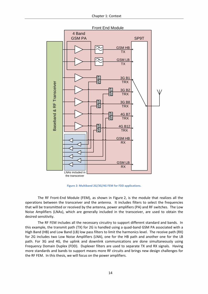
Figure 2: Multiband 2G/3G/4G FEM for FDD applications.
The RF Front-End Module (FEM), as shown in Figure 2, is the module that realizes all the operations between the transceiver and the antenna. It includes filters to select the frequencies that will be transmitted or received by the antenna, power amplifiers (PA) and RF switches. The Low Noise Amplifiers (LNAs), which are generally included in the transceiver, are used to obtain the desired sensitivity.
The RF FEM includes all the necessary circuitry to support different standard and bands. In this example, the transmit path (TX) for 2G is handled using a quad-band GSM PA associated with a High Band (HB) and Low Band (LB) low pass filters to limit the harmonics level. The receive path (RX) for 2G includes two Low Noise Amplifiers (LNA), one for the HB path and another one for the LB path. For 3G and 4G, the uplink and downlink communications are done simultaneously using Frequency Domain Duplex (FDD). Duplexer filters are used to separate TX and RX signals. Having more standards and bands to support means more RF circuits and brings new design challenges for the RF FEM. In this thesis, we will focus on the power amplifiers.
Ba
se
ba
nd
& R
F T
ran
sce
ive
r
4 Band
GSM PA
GSM HB
TX
GSM LB
TX
3G B1
TRX
3G B8
TRX
3G B2
TRX
4G B12
TRX
4G B7
TRX
GSM HB
RX
GSM LB
RX
SP9T
LNAs included in
the transceiver
Front End Module

Chapter 1: Context
15
I-3.2. RF Power Amplifier Module (PAM)
PA modules are essential in radio links since the transmit RF signal needs to be amplified at a high enough level to ensure quality of the transmission. Traditionally, PA modules (PAM) were optimized for a dedicated operation. However, with the growing number of standards, this strategy is reaching its limits in terms of cost and complexity [Walsh09]. In the following paragraphs, the evolution of multimode multiband PAM architectures will be discussed.
A. PAM architectures
a. Mode Specific PA architecture
Historically, when a new band or standard was required, the manufacturers simply added a discrete “mode specific” PA line-up in the RF FEM, as shown in Figure 2. The advantage of such approach is to have the best performance for each mode/standard while paying for exactly what is required.
Table 5: Performance of commercial “Mode Specific” Power Amplifiers.
Reference Standard Output Power Power Added Efficiency
[SKY77351-13] 2G (GSM) 35.5dBm 55%
[SKY77187] 3G (HSPA) 29dBm 40%
[SKY77709] 4G (LTE) 28dBm 36%
With the current evolution trend, this solution tends to be abandoned in favor of converged architectures which are more cost effective.
b. Converged PA architecture
In a converged PA architecture, the goal is to minimize the number of PA line-up while addressing multiple standard and frequency bands [Cheng11]. The block diagram of a converged PA architecture is shown in Figure 3.
Both PA line-ups must be able to reconfigure their operating mode according to the considered standard and frequency band. Tuning degrades to the performance of line-ups. Examples of performance for this type of PA are given in Table 6.
Table 6: Performances of converged 2G/3G PA with support of bands 5 and 8 [Kang13].
Mode Pout PAE ACPR
2G (GSM) 34.5dBm > 53% -
2.5G (EDGE) 29.0dBm > 27% -58dBc
3G (WCDMA) 28.2dBm > 41% -39dBc
Figure 3: Converged PA Architecture.
3G/4G-B13G/4G-B24G-B7
3G/4G-B84G-B12
2G-HB
2G-LB
Chapter 1: Context
16
To implement such architecture, either wideband or reconfigurable PA is required. Wideband power amplifiers have the advantage to minimize the complexity but have degraded performance due to the required broadband matching networks. On the other hand, reconfigurable PA (RPA) offer better performance in every band at the cost of a higher complexity since tunable components are needed.
B. Reconfigurable PA
a. Reconfigurable multi-mode PA
As discussed in previously, the different cellular standards have different types of requirements. GSM standard requires high output power with low linearity constraints. Therefore, highly efficient saturated PAs operating near saturation can be used. Others standards, such as LTE, require lower power with high PAPR and linearity constraints. For this last application, linear PAs operating in linear mode are required.
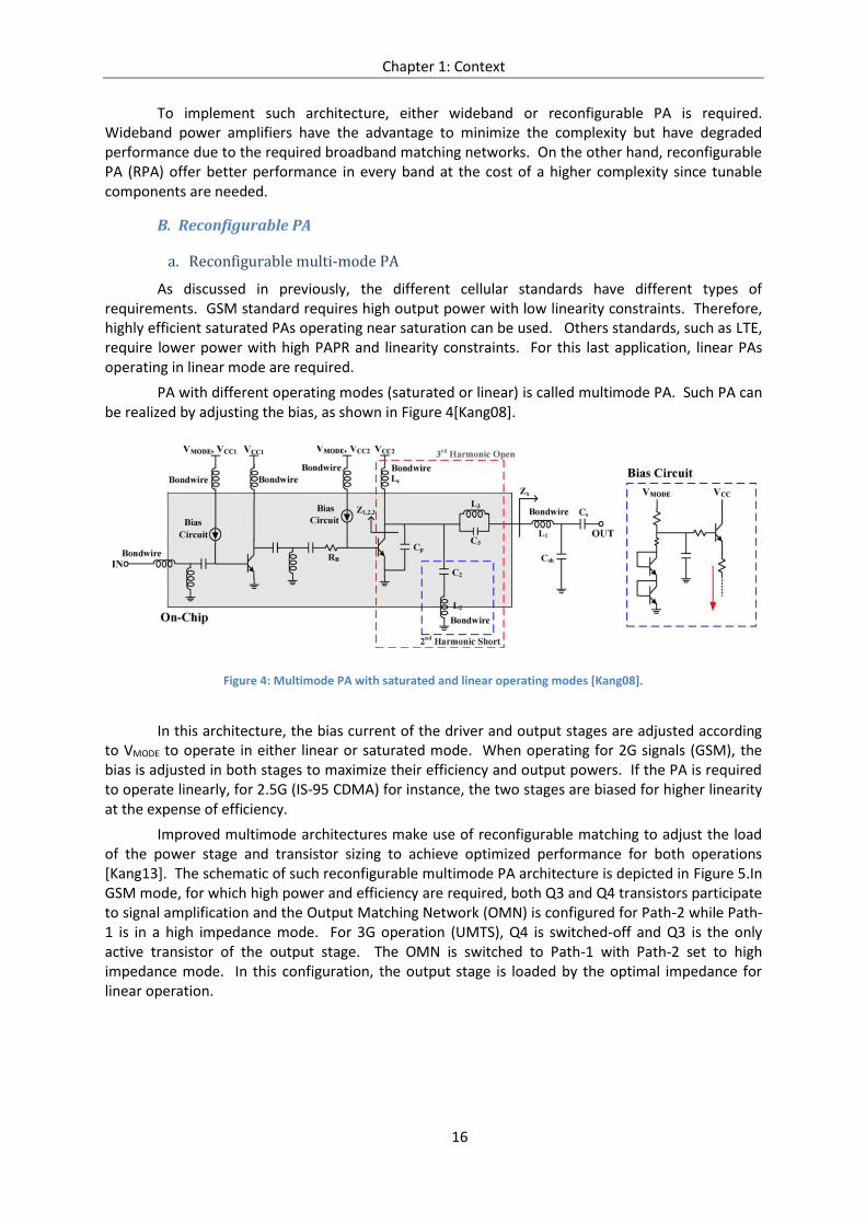
PA with different operating modes (saturated or linear) is called multimode PA. Such PA can be realized by adjusting the bias, as shown in Figure 4[Kang08].
Figure 4: Multimode PA with saturated and linear operating modes [Kang08].
In this architecture, the bias current of the driver and output stages are adjusted according to VMODE to operate in either linear or saturated mode. When operating for 2G signals (GSM), the bias is adjusted in both stages to maximize their efficiency and output powers. If the PA is required to operate linearly, for 2.5G (IS-95 CDMA) for instance, the two stages are biased for higher linearity at the expense of efficiency.
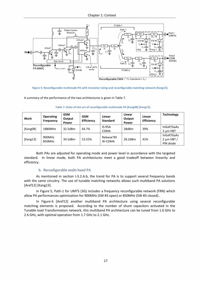
Improved multimode architectures make use of reconfigurable matching to adjust the load of the power stage and transistor sizing to achieve optimized performance for both operations [Kang13]. The schematic of such reconfigurable multimode PA architecture is depicted in Figure 5.In GSM mode, for which high power and efficiency are required, both Q3 and Q4 transistors participate to signal amplification and the Output Matching Network (OMN) is configured for Path-2 while Path-1 is in a high impedance mode. For 3G operation (UMTS), Q4 is switched-off and Q3 is the only active transistor of the output stage. The OMN is switched to Path-1 with Path-2 set to high impedance mode. In this configuration, the output stage is loaded by the optimal impedance for linear operation.
Chapter 1: Context
17
Figure 5: Reconfigurable multimode PA with transistor sizing and reconfigurable matching network [Kang13].
A summary of the performance of the two architectures is given in Table 7.
Table 7: State-of-the-art of reconfigurable multimode PA [Kang08] [Kang13].
Work Operating Frequency
GSM Output Power
GSM Efficiency
Linear Standard
Linear Output Power
Linear Efficiency
Technology
[Kang08] 1880MHz 32.5dBm 64.7% IS-95A CDMA
28dBm 39% InGaP/GaAs 2 µm HBT
[Kang13] 900MHz 850MHz
34.5dBm 53.55% Release’99 W-CDMA
28.2dBm 41% InGaP/GaAs 2 µm HBT / PIN diode
Both PAs are adjusted for operating mode and power level in accordance with the targeted standard. In linear mode, both PA architectures meet a good tradeoff between linearity and efficiency.
b. Reconfigurable multi-band PA
As mentioned in section I-3.2.A.b, the trend for PA is to support several frequency bands with the same circuitry. The use of tunable matching networks allows such multiband PA solutions [Aref12] [Kang13].
In Figure 5, Path-1 for UMTS (3G) includes a frequency reconfigurable network (FRN) which allow PA performances optimization for 900MHz (SW #3 open) or 850MHz (SW #3 closed)..
In Figure 6 [Aref12] another multiband PA architecture using several reconfigurable matching elements is proposed. According to the number of shunt capacitors activated in the Tunable load Transformation network, this multiband PA architecture can be tuned from 1.6 GHz to 2.6 GHz, with optimal operation from 1.7 GHz to 2.1 GHz.
Chapter 1: Context
18
Figure 6: Simplified schematic of a multiband saturated PA [Aref12].
c. Reconfigurable PA with multiple power levels
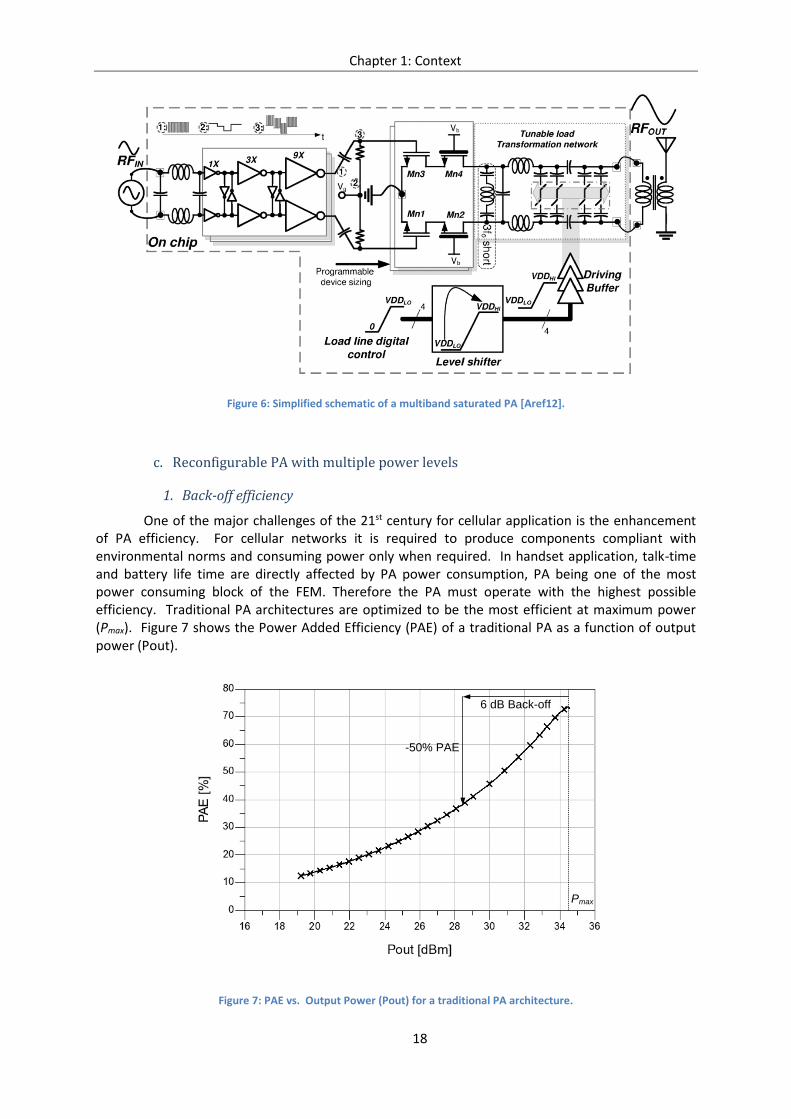
1. Back-off efficiency
One of the major challenges of the 21st century for cellular application is the enhancement of PA efficiency. For cellular networks it is required to produce components compliant with environmental norms and consuming power only when required. In handset application, talk-time and battery life time are directly affected by PA power consumption, PA being one of the most power consuming block of the FEM. Therefore the PA must operate with the highest possible efficiency. Traditional PA architectures are optimized to be the most efficient at maximum power (Pmax). Figure 7 shows the Power Added Efficiency (PAE) of a traditional PA as a function of output power (Pout).
Figure 7: PAE vs. Output Power (Pout) for a traditional PA architecture.
Pmax
6 dB Back-off
-50% PAE

Chapter 1: Context
19
In this graph we can notice that efficiency drops for low output power levels. In this example, if the required power is four times lower (6dB power back-off) than Pmax, PAE is reduced by a factor of two.
For constant envelope signals, PA linearity is not a concern and the PA line-up can be reconfigured in static manner to optimize its efficiency at each back-off power. PA efficiency can be optimized for different power levels while using multi-state architecture as shown in Figure 8.
Figure 8:PAE evolution vs. Output Power in a multi-power mode PA
Generally, the use of 3 states is sufficient for a correct improvement of efficiency. The added circuitry is simple and easy to drive. The static reconfiguration of PA efficiency is commonly done with transistor re-sizing and stage bypass architectures.
2. Power transistor re-sizing
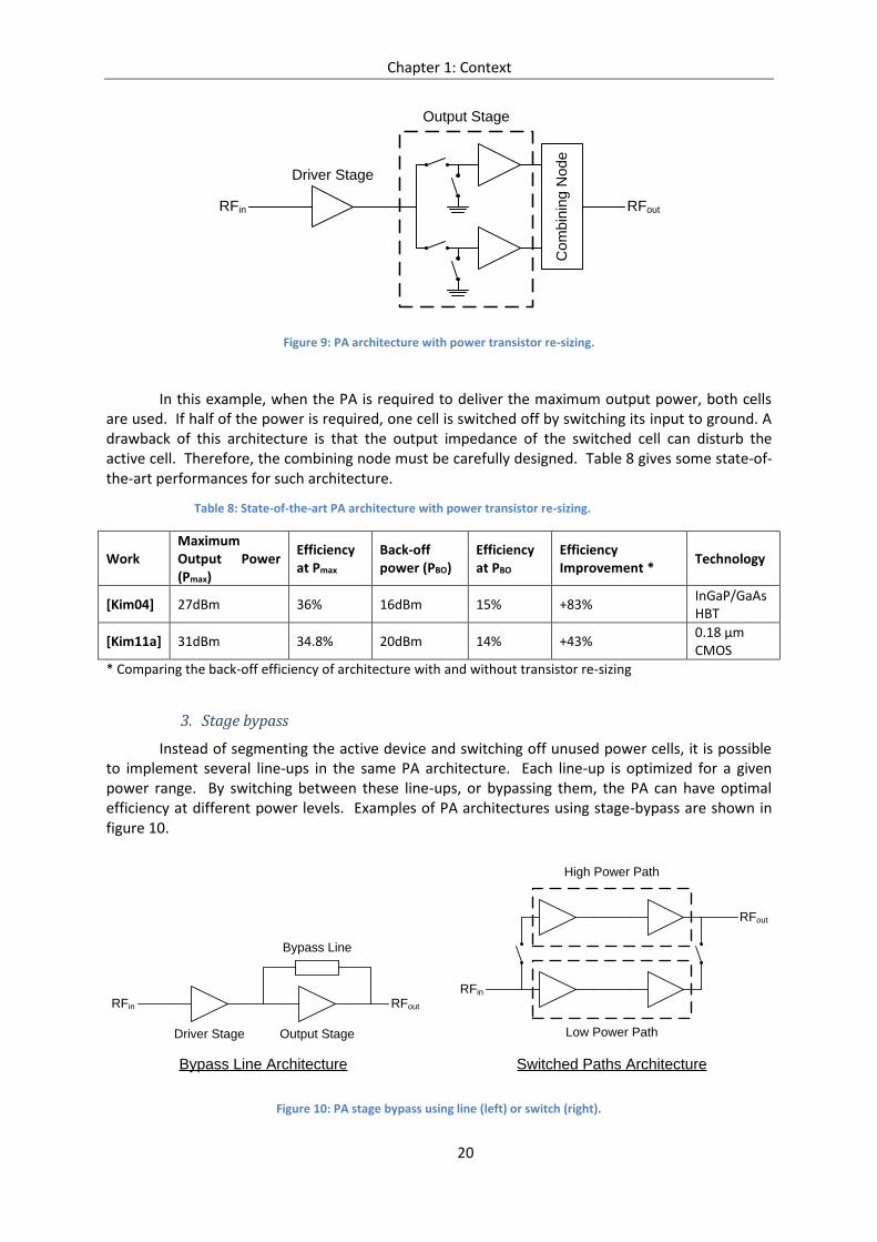
One type of PA architecture takes advantage from the bias strategy of segmented power devices. For a given power level, only the minimum number of power cell is biased [Kim04] [Kim11a]. The unused power cells are switched off to improve the overall efficiency of the PA. The block schematic of a PA architecture with power transistor re-sizing using 2 output cells is presented in Figure 9.
Fixed Power Cell
3-states Power Cell
Chapter 1: Context
20
Figure 9: PA architecture with power transistor re-sizing.
In this example, when the PA is required to deliver the maximum output power, both cells are used. If half of the power is required, one cell is switched off by switching its input to ground. A drawback of this architecture is that the output impedance of the switched cell can disturb the active cell. Therefore, the combining node must be carefully designed. Table 8 gives some state-of-the-art performances for such architecture.
Table 8: State-of-the-art PA architecture with power transistor re-sizing.
Work Maximum Output Power (Pmax)
Efficiency at Pmax
Back-off power (PBO)
Efficiency at PBO
Efficiency Improvement *
Technology
[Kim04] 27dBm 36% 16dBm 15% +83% InGaP/GaAs HBT
[Kim11a] 31dBm 34.8% 20dBm 14% +43% 0.18 µm CMOS
* Comparing the back-off efficiency of architecture with and without transistor re-sizing
3. Stage bypass
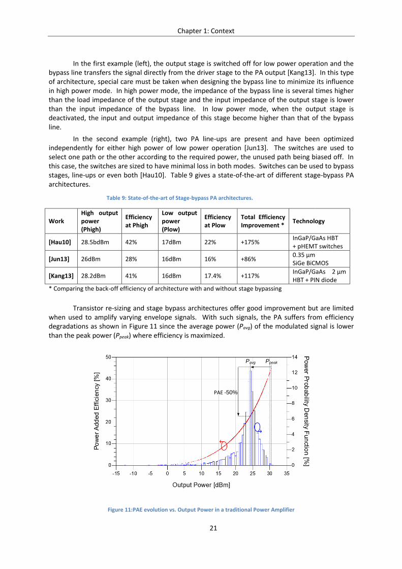
Instead of segmenting the active device and switching off unused power cells, it is possible to implement several line-ups in the same PA architecture. Each line-up is optimized for a given power range. By switching between these line-ups, or bypassing them, the PA can have optimal efficiency at different power levels. Examples of PA architectures using stage-bypass are shown in figure 10.
Figure 10: PA stage bypass using line (left) or switch (right).
Co
mb
inin
g N
od
e
Output Stage
RFin RFout
Driver Stage
RFin
RFout
High Power Path
Low Power Path
Switched Paths Architecture
Output Stage
RFin
Driver Stage
RFout
Bypass Line
Bypass Line Architecture
Chapter 1: Context
21
In the first example (left), the output stage is switched off for low power operation and the bypass line transfers the signal directly from the driver stage to the PA output [Kang13]. In this type of architecture, special care must be taken when designing the bypass line to minimize its influence in high power mode. In high power mode, the impedance of the bypass line is several times higher than the load impedance of the output stage and the input impedance of the output stage is lower than the input impedance of the bypass line. In low power mode, when the output stage is deactivated, the input and output impedance of this stage become higher than that of the bypass line.
In the second example (right), two PA line-ups are present and have been optimized independently for either high power of low power operation [Jun13]. The switches are used to select one path or the other according to the required power, the unused path being biased off. In this case, the switches are sized to have minimal loss in both modes. Switches can be used to bypass stages, line-ups or even both [Hau10]. Table 9 gives a state-of-the-art of different stage-bypass PA architectures.
Table 9: State-of-the-art of Stage-bypass PA architectures.
Work High output power (Phigh)
Efficiency at Phigh
Low output power (Plow)
Efficiency at Plow
Total Efficiency Improvement *
Technology
[Hau10] 28.5bdBm 42% 17dBm 22% +175% InGaP/GaAs HBT + pHEMT switches
[Jun13] 26dBm 28% 16dBm 16% +86% 0.35 µm SiGe BiCMOS
[Kang13] 28.2dBm 41% 16dBm 17.4% +117% InGaP/GaAs 2 µm HBT + PIN diode
* Comparing the back-off efficiency of architecture with and without stage bypassing
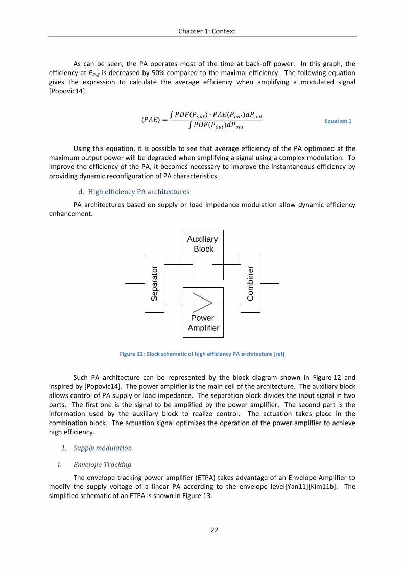
Transistor re-sizing and stage bypass architectures offer good improvement but are limited when used to amplify varying envelope signals. With such signals, the PA suffers from efficiency degradations as shown in Figure 11 since the average power (Pavg) of the modulated signal is lower than the peak power (Ppeak) where efficiency is maximized.
Figure 11:PAE evolution vs. Output Power in a traditional Power Amplifier
PpeakPavg
PAE -50%
Chapter 1: Context
22
As can be seen, the PA operates most of the time at back-off power. In this graph, the efficiency at Pavg is decreased by 50% compared to the maximal efficiency. The following equation gives the expression to calculate the average efficiency when amplifying a modulated signal [Popovic14].
⟨𝑃𝐴𝐸⟩ =∫𝑃𝐷𝐹(𝑃𝑜𝑢𝑡) ∙ 𝑃𝐴𝐸(𝑃𝑜𝑢𝑡)𝑑𝑃𝑜𝑢𝑡
∫𝑃𝐷𝐹(𝑃𝑜𝑢𝑡)𝑑𝑃𝑜𝑢𝑡 Equation 1
Using this equation, it is possible to see that average efficiency of the PA optimized at the maximum output power will be degraded when amplifying a signal using a complex modulation. To improve the efficiency of the PA, it becomes necessary to improve the instantaneous efficiency by providing dynamic reconfiguration of PA characteristics.
d. High efficiency PA architectures
PA architectures based on supply or load impedance modulation allow dynamic efficiency enhancement.
Figure 12: Block schematic of high efficiency PA architecture [ref]
Such PA architecture can be represented by the block diagram shown in Figure 12 and inspired by [Popovic14]. The power amplifier is the main cell of the architecture. The auxiliary block allows control of PA supply or load impedance. The separation block divides the input signal in two parts. The first one is the signal to be amplified by the power amplifier. The second part is the information used by the auxiliary block to realize control. The actuation takes place in the combination block. The actuation signal optimizes the operation of the power amplifier to achieve high efficiency.
1. Supply modulation
i. Envelope Tracking
The envelope tracking power amplifier (ETPA) takes advantage of an Envelope Amplifier to modify the supply voltage of a linear PA according to the envelope level[Yan11][Kim11b]. The simplified schematic of an ETPA is shown in Figure 13.
Se
pa
rato
r
Co
mb
ine
r
Auxiliary
Block
Power
Amplifier
Chapter 1: Context
23
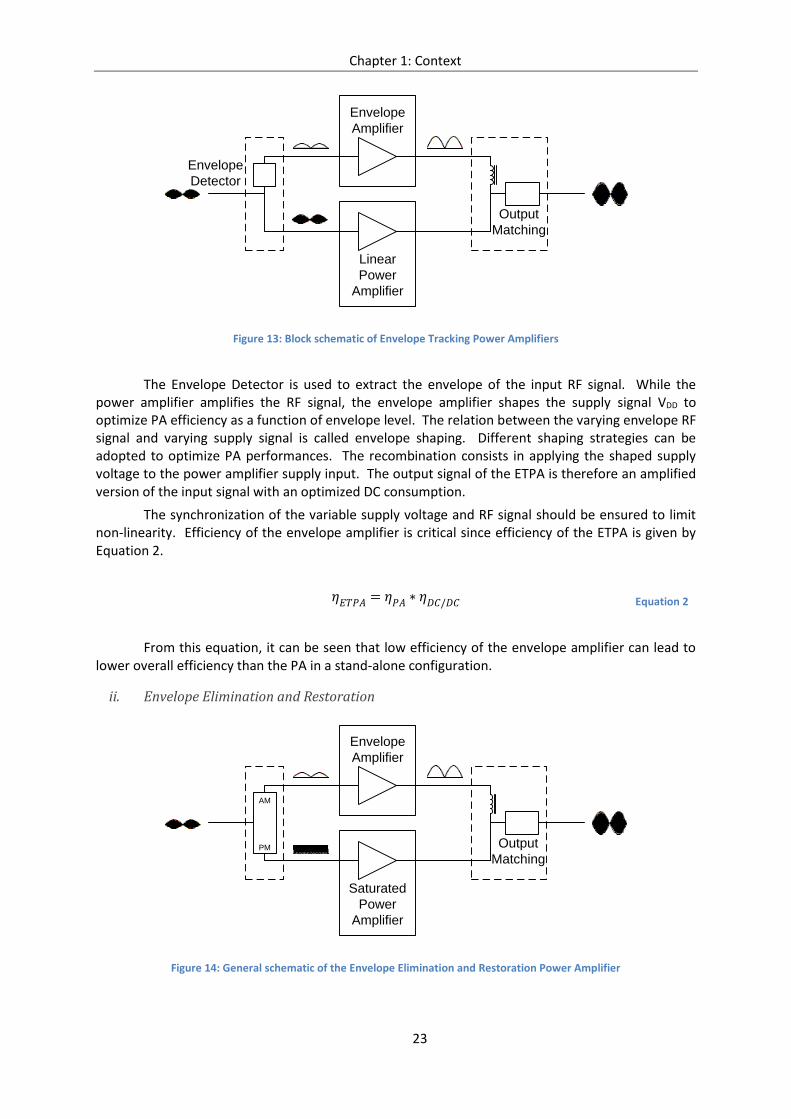
Figure 13: Block schematic of Envelope Tracking Power Amplifiers
The Envelope Detector is used to extract the envelope of the input RF signal. While the power amplifier amplifies the RF signal, the envelope amplifier shapes the supply signal VDD to optimize PA efficiency as a function of envelope level. The relation between the varying envelope RF signal and varying supply signal is called envelope shaping. Different shaping strategies can be adopted to optimize PA performances. The recombination consists in applying the shaped supply voltage to the power amplifier supply input. The output signal of the ETPA is therefore an amplified version of the input signal with an optimized DC consumption.
The synchronization of the variable supply voltage and RF signal should be ensured to limit non-linearity. Efficiency of the envelope amplifier is critical since efficiency of the ETPA is given by Equation 2.
𝜂𝐸𝑇𝑃𝐴 = 𝜂𝑃𝐴 ∗ 𝜂𝐷𝐶/𝐷𝐶 Equation 2
From this equation, it can be seen that low efficiency of the envelope amplifier can lead to lower overall efficiency than the PA in a stand-alone configuration.
ii. Envelope Elimination and Restoration
Figure 14: General schematic of the Envelope Elimination and Restoration Power Amplifier
Envelope
Detector
Output
Matching
Envelope
Amplifier
Linear
Power
Amplifier
Output
Matching
Envelope
Amplifier
Saturated
Power
Amplifier
AM
PM
Chapter 1: Context
24
The block schematic of an Envelope Elimination and Restoration (EER) PA is shown in Figure 14. This architecture is very similar to the envelope tracking. There is however significant differences in its operation. The EER PA uses a total separation of the Amplitude Modulation (AM) and Phase Modulation (PM) of the complex signal [Pinon08] [Kim10]. The AM signal is sent to the envelope amplifier to generate the supply signal of a saturated PA. The DC/DC converter in the case of EER has more precision constraint than ETPA as the shaped supply is used to restore the AM component of the modulation to the output signal.
The PM signal is amplified by the PA. As this signal has a constant envelope, the PA can be designed for a highly efficient switching class. The full modulation is restored thanks to the supply voltage of the PA which will be the image of the signal Envelope. Synchronization between the shaped supply and the amplified PM signals is crucial. The least synchronization issue can lead to high distortion of the output signal. Also, the efficiency of the envelope amplifier cannot be neglected in the overall efficiency of an EER PA, as it was the case for the ETPA.
2. Load Modulation
i. Doherty Power Amplifiers
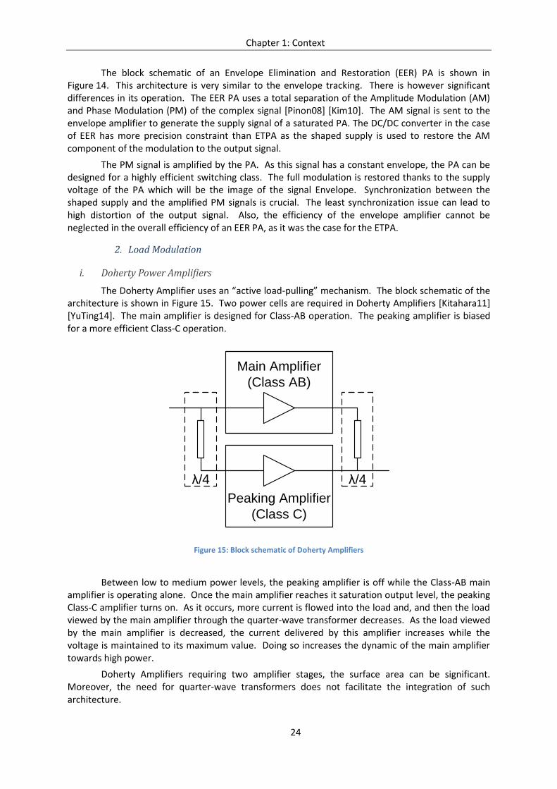
The Doherty Amplifier uses an “active load-pulling” mechanism. The block schematic of the architecture is shown in Figure 15. Two power cells are required in Doherty Amplifiers [Kitahara11] [YuTing14]. The main amplifier is designed for Class-AB operation. The peaking amplifier is biased for a more efficient Class-C operation.
Figure 15: Block schematic of Doherty Amplifiers
Between low to medium power levels, the peaking amplifier is off while the Class-AB main amplifier is operating alone. Once the main amplifier reaches it saturation output level, the peaking Class-C amplifier turns on. As it occurs, more current is flowed into the load and, and then the load viewed by the main amplifier through the quarter-wave transformer decreases. As the load viewed by the main amplifier is decreased, the current delivered by this amplifier increases while the voltage is maintained to its maximum value. Doing so increases the dynamic of the main amplifier towards high power.
Doherty Amplifiers requiring two amplifier stages, the surface area can be significant. Moreover, the need for quarter-wave transformers does not facilitate the integration of such architecture.
Main Amplifier
(Class AB)
Peaking Amplifier
(Class C)
λ/4λ/4

Chapter 1: Context
25
ii. Passive Load Modulation
The passive load modulation is the passive equivalent of the Doherty Amplifier. The general schematic of such architecture is given in Figure 16.
Figure 16: Passive Load Modulation Power Amplifier block schematic
This architecture relies on a Tunable Matching Network (TMN) to modify the load impedance viewed by the PA [Yue12] [Andersson12]. The TMN is actuated by a control signal generated from the envelope information. This can either be done by detecting the envelope of the RF signal or by directly using the baseband information.
𝜂𝑡𝑜𝑡 = 𝜂𝑃𝐴+𝐶𝑇𝑅𝐿 ∙ 𝐼𝐿𝑇𝑀𝑁 =𝑃𝑜𝑢𝑡
𝑃𝐷𝐶𝑃𝐴 +𝑃𝐷𝐶𝐶𝑇𝑅𝐿∙ 𝐼𝐿𝑇𝑀𝑁 Equation 3
The drawback of this technique is the increased loss in the TMN compared to a fixed network. A rough estimation of the loss impact is given in Equation 3. In this formula, the efficiency of the power amplifier should include the consumption of the control processing block PDC CTRL. Moreover, the loss of the TMN (ILTMN) should not be too high in order to not decrease the overall efficiency. Furthermore, bad synchronization between the TMN actuation and RF signal can lead to distortion in the RF signal.
3. Impact on linearity
All the architecture presented above can distort the signal. In that case, a linearization technique can be added in order to meet the linearity requirement of the considered standard. The consumption of the linearization circuit impacts the efficiency of the full architecture. In the case of handset PA, the consumption of the linearization circuit mitigates the efficiency enhancement [Cripps06].
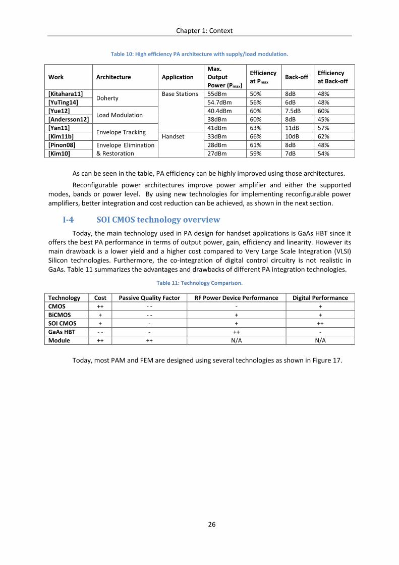
Table 10presents a state-of-the-art of high efficiency PA architectures using supply and load modulation, for both handset and base station applications.
Envelope
Detector
TMN
Power
Amplifier
Control
Processing
Chapter 1: Context
26
Table 10: High efficiency PA architecture with supply/load modulation.
Work Architecture Application Max. Output Power (Pmax)
Efficiency at Pmax
Back-off Efficiency at Back-off
[Kitahara11] Doherty
Base Stations 55dBm 50% 8dB 48%
[YuTing14] 54.7dBm 56% 6dB 48%
[Yue12] Load Modulation
40.4dBm 60% 7.5dB 60%
[Andersson12] 38dBm 60% 8dB 45%
[Yan11] Envelope Tracking
41dBm 63% 11dB 57%
[Kim11b] Handset 33dBm 66% 10dB 62%
[Pinon08] Envelope Elimination & Restoration
28dBm 61% 8dB 48%
[Kim10] 27dBm 59% 7dB 54%
As can be seen in the table, PA efficiency can be highly improved using those architectures.
Reconfigurable power architectures improve power amplifier and either the supported modes, bands or power level. By using new technologies for implementing reconfigurable power amplifiers, better integration and cost reduction can be achieved, as shown in the next section.
I-4 SOI CMOS technology overview
Today, the main technology used in PA design for handset applications is GaAs HBT since it offers the best PA performance in terms of output power, gain, efficiency and linearity. However its main drawback is a lower yield and a higher cost compared to Very Large Scale Integration (VLSI) Silicon technologies. Furthermore, the co-integration of digital control circuitry is not realistic in GaAs. Table 11 summarizes the advantages and drawbacks of different PA integration technologies.
Table 11: Technology Comparison.
Technology Cost Passive Quality Factor RF Power Device Performance Digital Performance
CMOS ++ - - - +
BiCMOS + - - + +
SOI CMOS + - + ++
GaAs HBT - - - ++ -
Module ++ ++ N/A N/A
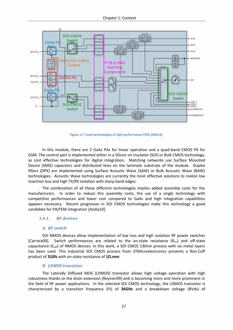
Today, most PAM and FEM are designed using several technologies as shown in Figure 17.
Chapter 1: Context
27
Figure 17: Used technologies in high performance FEM [ASN13].
In this module, there are 2 GaAs PAs for linear operation and a quad-band CMOS PA for GSM. The control part is implemented either in a Silicon on Insulator (SOI) or Bulk CMOS technology, as cost effective technologies for digital integration. Matching networks use Surface Mounted Device (SMD) capacitors and distributed lines on the laminate substrate of the module. Duplex filters (DPX) are implemented using Surface Acoustic Wave (SAW) or Bulk Acoustic Wave (BAW) technologies. Acoustic Wave technologies are currently the most effective solutions to realize low insertion loss and high TX/RX isolation with sharp band edges.
The combination of all these different technologies implies added assembly costs for the manufacturers. In order to reduce this assembly costs, the use of a single technology with competitive performances and lower cost compared to GaAs and high integration capabilities appears necessary. Recent progresses in SOI CMOS technologies make this technology a good candidate for PA/FEM integration [Andia10].
I-4.1. RF devices
A. RF switch
SOI NMOS devices allow implementation of low loss and high isolation RF power switches [Carrara09]. Switch performances are related to the on-state resistance (Ron) and off-state capacitance (Coff) of NMOS devices. In this work, a SOI CMOS 130nm process with six metal layers has been used. This industrial SOI CMOS process from STMicroelectronics presents a Ron.Coff product of 310fs with on-state resistance of 1Ω.mm.
B. LDMOS transistor
The Laterally Diffused MOS (LDMOS) transistor allows high voltage operation with high robustness thanks to the drain extension [Reynier09] and is becoming more and more prominent in the field of RF power applications. In the selected SOI CMOS technology, the LDMOS transistor is characterized by a transition frequency (Ft) of 36GHz and a breakdown voltage (BVds) of
CMOS PA
GaAs PA
GaAs PA
SOI-CMOS
Switch
SOI-CMOS
Switch
SOI-CMOS
Switch
CMOS/SOI-CMOS
ControlPCB & SMD
Matching
Components
Chapter 1: Context
28
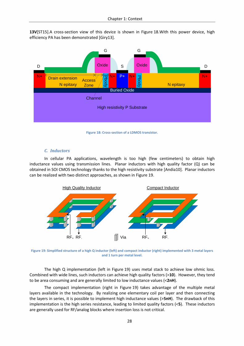
13V[ST15].A cross-section view of this device is shown in Figure 18.With this power device, high efficiency PA has been demonstrated [Giry13].
Figure 18: Cross-section of a LDMOS transistor.
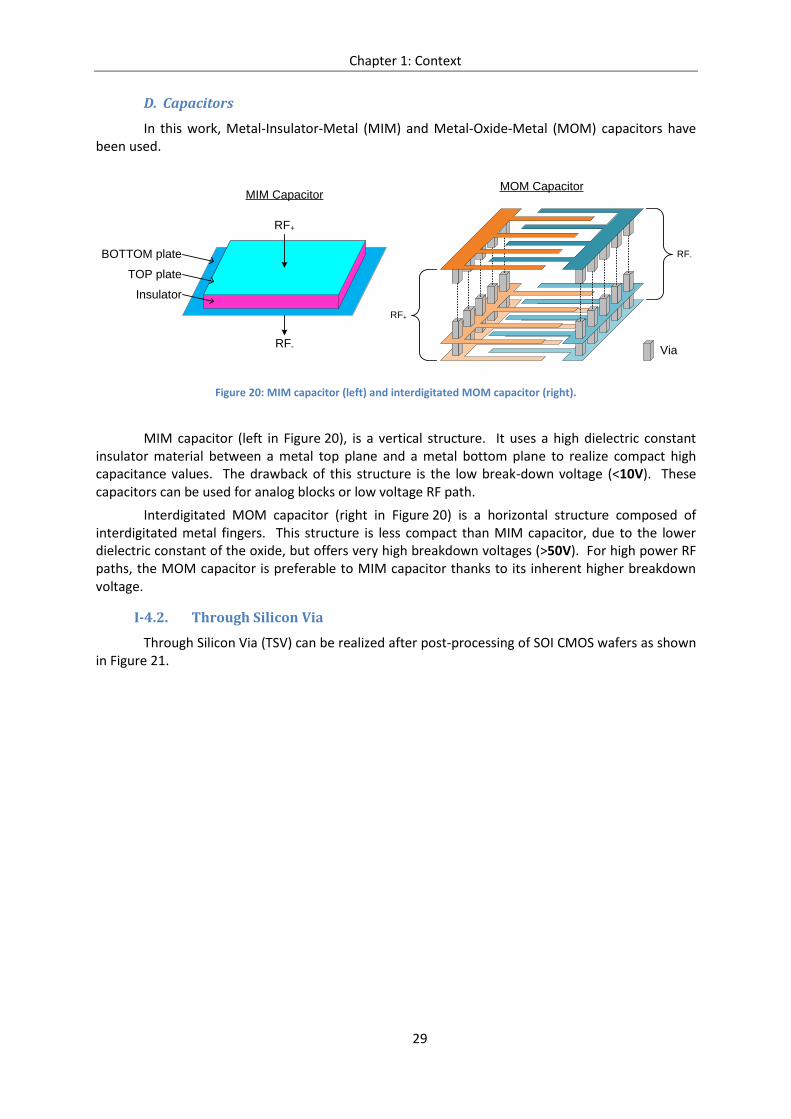
C. Inductors
In cellular PA applications, wavelength is too high (few centimeters) to obtain high inductance values using transmission lines. Planar inductors with high quality factor (Q) can be obtained in SOI CMOS technology thanks to the high resistivity substrate [Andia10]. Planar inductors can be realized with two distinct approaches, as shown in Figure 19.
Figure 19: Simplified structure of a high Q inductor (left) and compact inductor (right) implemented with 3 metal layers and 1 turn per metal level.
The high Q implementation (left in Figure 19) uses metal stack to achieve low ohmic loss. Combined with wide lines, such inductors can achieve high quality factors (>10). However, they tend to be area consuming and are generally limited to low inductance values (<2nH).
The compact implementation (right in Figure 19) takes advantage of the multiple metal layers available in the technology. By realizing one elementary coil per layer and then connecting the layers in series, it is possible to implement high inductance values (>5nH). The drawback of this implementation is the high series resistance, leading to limited quality factors (<5). These inductors are generally used for RF/analog blocks where insertion loss is not critical.
High resistivity P Substrate
Buried Oxide
Pb
od
y
P+ N+N+
N epitaxy N epitaxy
N+ N+
Oxide OxideD DS
G G
Drain extensionAccess
Zone
Pb
od
y
Channel
Compact Inductor
RF-RF+
High Quality Inductor
RF-RF+ Via
Chapter 1: Context
29
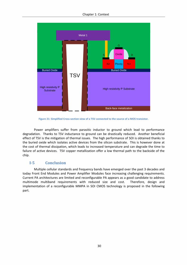
D. Capacitors
In this work, Metal-Insulator-Metal (MIM) and Metal-Oxide-Metal (MOM) capacitors have been used.
Figure 20: MIM capacitor (left) and interdigitated MOM capacitor (right).
MIM capacitor (left in Figure 20), is a vertical structure. It uses a high dielectric constant insulator material between a metal top plane and a metal bottom plane to realize compact high capacitance values. The drawback of this structure is the low break-down voltage (<10V). These capacitors can be used for analog blocks or low voltage RF path.
Interdigitated MOM capacitor (right in Figure 20) is a horizontal structure composed of interdigitated metal fingers. This structure is less compact than MIM capacitor, due to the lower dielectric constant of the oxide, but offers very high breakdown voltages (>50V). For high power RF paths, the MOM capacitor is preferable to MIM capacitor thanks to its inherent higher breakdown voltage.
I-4.2. Through Silicon Via
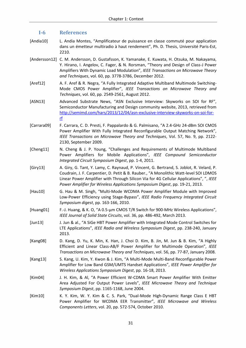
Through Silicon Via (TSV) can be realized after post-processing of SOI CMOS wafers as shown in Figure 21.
MIM Capacitor
Insulator
TOP plate
BOTTOM plate
RF+
RF- Via
RF-
RF+
MOM Capacitor
Chapter 1: Context
30
Figure 21: Simplified Cross-section view of a TSV connected to the source of a MOS transistor.
Power amplifiers suffer from parasitic inductor to ground which lead to performance degradation. Thanks to TSV inductance to ground can be drastically reduced. Another beneficial effect of TSV is the mitigation of thermal issues. The high performance of SOI is obtained thanks to the buried oxide which isolates active devices from the silicon substrate. This is however done at the cost of thermal dissipation, which leads to increased temperature and can degrade the time to failure of active devices. TSV copper metallization offer a low thermal path to the backside of the chip.
I-5 Conclusion
Multiple cellular standards and frequency bands have emerged over the past 3 decades and today Front End Modules and Power Amplifier Modules face increasing challenging requirements. Current PA architectures are limited and reconfigurable PA appears as a good candidate to address multimode multiband requirements with reduced size and cost. Therefore, design and implementation of a reconfigurable MMPA in SOI CMOS technology is proposed in the following part.
High resistivity P Substrate
Buried Oxide
Pbody N+
Oxide DS
G
High resistivity P
Substrate
Buried Oxide
N+
Metal 1
TSV
Back-face metalization
Chapter 1: Context
31
I-6 References
[Andia10] L. Andia Montes, “Amplificateur de puissance en classe commuté pour application dans un émetteur multiradio à haut rendement”, Ph. D. Thesis, Université Paris-Est, 2210.
[Andersson12] C. M. Andersson, D. Gustafsson, K. Yamanake, E. Kuwata, H. Otsuka, M. Nakayama, Y. Hirano, I. Angelov, C. Fager, & N. Rorsman, “Theory and Design of Class-J Power Amplifiers With Dynamic Load Modulation”, IEEE Transactions on Microwave Theory and Techniques, vol. 60, pp. 3778-3786, December 2012.
[Aref12] A. F. Aref & R. Negra, “A Fully Integrated Adaptive Multiband Multimode Switching-Mode CMOS Power Amplifier”, IEEE Transactions on Microwave Theory and Techniques, vol. 60, pp. 2549-2561, August 2012.
[ASN13] Advanced Substrate News, “ASN Exclusive Interview: Skyworks on SOI for RF”, Semiconductor Manufacturing and Design community website, 2013, retrieved from http://semimd.com/hars/2013/12/04/asn-exclusive-interview-skyworks-on-soi-for-rf
[Carrara09] F. Carrara, C. D. Presti, F. Pappalardo & G. Palmisano, “A 2.4-GHz 24-dBm SOI CMOS Power Amplifier With Fully Integrated Reconfigurable Output Matching Network”, IEEE Transactions on Microwave Theory and Techniques, Vol. 57, No. 9, pp. 2122-2130, September 2009.
[Cheng11] N. Cheng & J. P. Young, “Challenges and Requirements of Multimode Multiband Power Amplifiers for Mobile Applications”, IEEE Compound Semiconductor Integrated Circuit Symposium Digest, pp. 1-4, 2011.
[Giry13] A. Giry, G. Tant, Y. Lamy, C. Raynaud, P. Vincent, G. Bertrand, S. Joblot, R. Velard, P. Coudrain, J. F. Carpentier, D. Petit & B. Rauber., “A Monolithic Watt-level SOI LDMOS Linear Power Amplifier with Through Silicon Via for 4G Cellular Applications”, ”, IEEE Power Amplifier for Wireless Applications Symposium Digest, pp. 19-21, 2013.
[Hau10] G. Hau & M. Singh, “Multi-Mode WCDMA Power Amplifier Module with Improved Low-Power Efficiency using Stage-Bypass”, IEEE Radio Frequency Integrated Circuit Symposium digest, pp. 163-166, 2010.
[Huang01] F.-J. Huang, & K. O, “A 0.5-µm CMOS T/R Switch for 900-MHz Wireless Applications”, IEEE Journal of Solid State Circuits, vol. 36, pp. 486-492, March 2013.
[Jun13] J. Jun & al., “A SiGe HBT Power Amplifier with Integrated Mode Control Switches for LTE Applications”, IEEE Radio and Wireless Symposium Digest, pp. 238-240, January 2013.
[Kang08] D. Kang, D. Yu, K. Min, K. Han, J. Choi D. Kim, B. Jin, M. Jun & B. Kim, “A Highly Efficient and Linear Class-AB/F Power Amplifier for Multimode Operation”, IEEE Transactions on Microwave Theory and Techniques, vol. 56, pp. 77-87, January 2008.
[Kang13] S. Kang, U. Kim, Y. Kwon & J. Kim, “A Multi-Mode Multi-Band Reconfigurable Power Amplifier for Low Band GSM/UMTS Handset Applications”, IEEE Power Amplifier for Wireless Applications Symposium Digest, pp. 16-18, 2013.
[Kim04] J. H. Kim, & Al, “A Power Efficient W-CDMA Smart Power Amplifier With Emitter Area Adjusted For Output Power Levels”, IEEE Microwave Theory and Technique Symposium Digest, pp. 1165-1168, June 2004.
[Kim10] K. Y. Kim, W. Y. Kim & C. S. Park, “Dual-Mode High-Dynamic Range Class E HBT Power Amplifier for WCDMA EER Transmitter”, IEEE Microwave and Wireless Components Letters, vol. 20, pp. 572-574, October 2010.

Chapter 1: Context
32
[Kim11a] J. Kim, K. Y. Kim, Y. H. Choi & C. S. Park, “A Linear Multi-Mode CMOS Power Amplifier With Discrete Resizing and Concurrent Power Combining Structure”, IEEE Journal on Solid State Circuit, vol. 46, pp. 1034-1048, May 2011.
[Kim11b] D. Kim, D. Kang, J. Choi, J. Kim, Y. Cho & B. Kim, “Optimization for Envelop Shaped Operation of Envelope Tracking Power Amplifier”, IEEE Transactions on Microwave Theory and Techniques, vol. 59, pp. 1787-1795, July 2011.
[Kitahara11] T. Kitahara, T Yamamoto & S. Hiura, “Doherty Power Amplifier with Asymmetrical Drain Voltages for Enhanced Efficiency at 8dB Backed-off Output Power”, IEEE Microwave Theory and Technique Symposium Digest, pp. 1-4, June 2011.
[Pinon08] V. Pinon, F. Hasbani, A. Giry, D. Pache & C. Garnier, “A Single-Chip WCDMA Envelope Reconstruction LDMS PA with 130MHz Switched-Mode Power Supply”, IEEE International Solid State Circuit Conference Digest, pp. 564-636, February 2008.
[Popovic14] Z. Popovic, T. Reveyrand, D. Sardin, M. Litchfield, S. Schaffer and A. Zai, “Design and measurements of high efficiency PAs with high PAR signals”, IEEE; Microwave Measurement Conference (ARFTG) workshop presentation, December 2014
[Reynier09] P. Reynier, “Intégration monolithique d’amplificateurs de puissance multi-bandes à fort rendement pour applications cellulaires”, Ph. D. Thesis, Institut National des Sciences Appliquées de Lyon, 2009.
[SKY77187] Skyworks Inc., “SKY77187 Power Amplifier Module for WCDMA / HSPA Band II (1850—1910MHz)”, Product Datasheet, retrieved from http://www.skyworksinc.com/uploads/documents/201011A.pdf
[SKY77709] Skyworks Inc., “SKY77709 Power Amplifier Module for LTE FDD Band VII (2300—2400MHz)”, Product Datasheet, retrieved from http://www.skyworksinc.com/uploads/documents/201229a.pdf
[SKY77351-13] Skyworks Inc., “SKY77351-13 Power Amplifier Module for Quad-Band GSM / GPRS / EDGE”, Product Datasheet, retrieved from http://www.skyworksinc.com/uploads/documents/201810a.pdf
[SKY77752] Skyworks Inc., “SKY77752 Dual-Band Power Amplifier Module for CDMA2000 / WCDMA / HSDPA / HSUPA Band II (1850—1910MHz) Band V (824—849MHz), LTE”, Product Datasheet, retrieved from http://www.skyworksinc.com/uploads/documents/SKY77752_201823B.pdf
[SKY77350-13] Skyworks Inc., “SKY77350-13 Power Amplifier Module for Quad-Band GSM / GPRS”, Product Datasheet, retrieved from http://www.skyworksinc.com/uploads/documents/201782a.pdf
[ST15] ST Microelectronics, “H9SOI_FEM Technology offer”, technology information document, retrieved from http://cmp.imag.fr/events/H9SOIFEM_Overview_CMP_Mar-15.pdf
[Tinella03] C. Tinella, J.-M. Fournier, D. Belot &V. Knopik, “A High-Performance CMOS-SOI Antenna Switch for the 2.5—5-GHz Band”, IEEE Journal of Solid State Circuits, vol. 38, pp. 1279-1283, July 2013.
[Walsh09] K. Walsh & J. Johnson, “3G/4G Multimode Cellular Front End Challenges”, RFMD White Paper, 2009.
[Yan11] J. J. Yan, C. Hsia, D. F. Kimbal, & P. M. Asbeck, “GaN Envelope Tracking Power Amplifier With More Than One Octave Carrier Bandwidth”, IEEE Compound Semiconductor Integrated Circuit Symposium Digest, pp. 1-4, October 2011.

Chapter 1: Context
33
[Yue12] L. Yue, T. Maehata, K. Totani, H. Tango, T. Hashinaga & T. Asaina, “A Novel Tunable Matching Network for Dynamic Load Modulation of High Power amplifiers”, IEEE European Radar Conference Proc., pp. 381-384, November 2012.
[YuTing14] D. Yu-Ting, J. Annes, M. Bokatius, P. Hart, E. Krvavac & G. Tucker, “A 350 W, 790 to 960MHz Wideband LDMOS Doherty Amplifier using a Modified Combining Scheme”, IEEE Microwave Theory and Technique Symposium Digest, pp. 1-4, June 2014.

Chapter 1: Context
34

35
Chapter II: Power Amplifier Design
1 Introduction
The previous chapter presented the context of this work as well as a state of the art of reconfigurable RF power amplifiers (PA). The design of reconfigurable PA requires first a basic knowledge of classic power amplifier design.
The following chapter first presents definitions and main characteristics commonly used in power amplifier design. The parameters presented in this part are used throughout the proposed research work and main buildings blocks for power amplifier design are presented.
An analytical analysis of different PA operating classes is then carried on in order to find trade-offs for the design of active stages. Two different cases are considered since saturated and linear PA designs need different optimizations regarding their respective specifications. Saturated PA are used for constant envelope signals, such as GSM. The main focus of the design is therefore the maximization of the efficiency. Linear PA are used for complex modulated signals with varying envelope and phase, such as 3G or 4G signals. This type of signal requires specific linearity performance which depends onto the considered standard. These linearity constraints can be used with proposed method in order to find the best trade-off.
The matching networks are used to present optimal source and load impedances to the active stage, thus ensuring their proper operation. Matching networks in this work are split in unit L-Cells. The number and size of these unit elements can be determined by using bandwidth and insertion loss requirements.
Matching networks can be made reconfigurable using tunable components such as switched capacitors. Therefore, the design of switched capacitor banks taking into account that those components must operate under high power levels is also presented.
Finally, the design of a single pole multiple throw RF switch is introduced in section II-5 since it represents a critical building block of multiband PA design.
Chapter 2: Power amplifier building blocks
36
II-1 Power amplifier characteristics
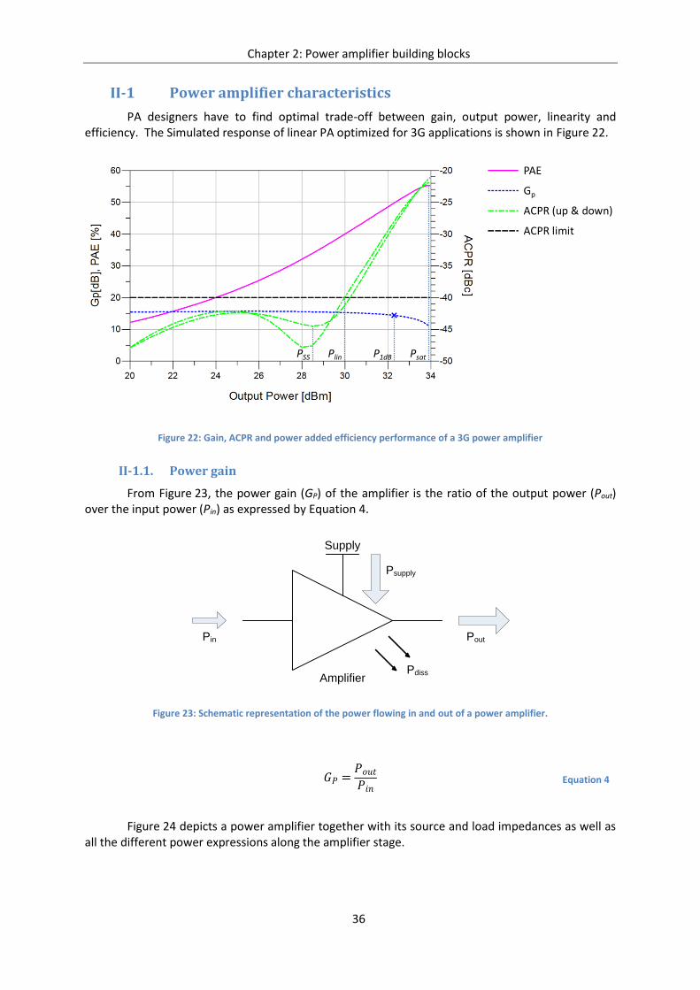
PA designers have to find optimal trade-off between gain, output power, linearity and efficiency. The Simulated response of linear PA optimized for 3G applications is shown in Figure 22.
Figure 22: Gain, ACPR and power added efficiency performance of a 3G power amplifier
II-1.1. Power gain
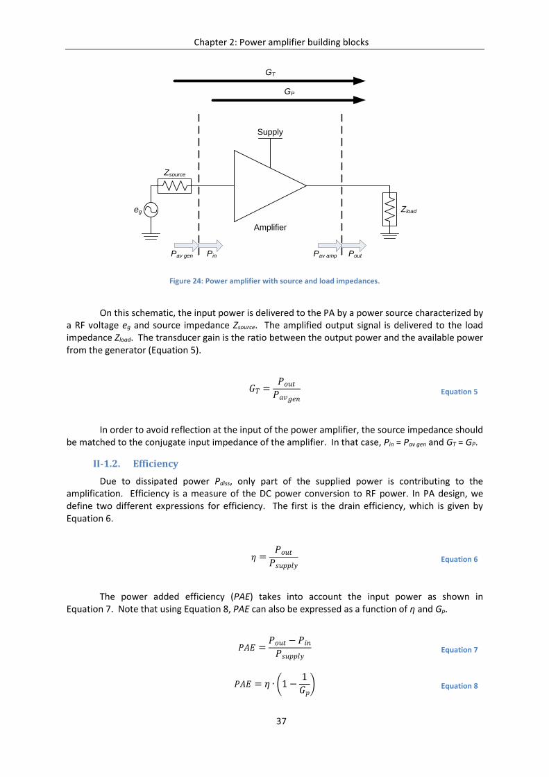
From Figure 23, the power gain (GP) of the amplifier is the ratio of the output power (Pout) over the input power (Pin) as expressed by Equation 4.
Figure 23: Schematic representation of the power flowing in and out of a power amplifier.
𝐺𝑃 =𝑃𝑜𝑢𝑡𝑃𝑖𝑛
Equation 4
Figure 24 depicts a power amplifier together with its source and load impedances as well as all the different power expressions along the amplifier stage.
PAE
Gp
ACPR (up & down)
ACPR limit
PSS Plin P1dB Psat
Amplifier
Supply
Pin Pout
Psupply
Pdiss
Chapter 2: Power amplifier building blocks
37
Figure 24: Power amplifier with source and load impedances.
On this schematic, the input power is delivered to the PA by a power source characterized by a RF voltage eg and source impedance Zsource. The amplified output signal is delivered to the load impedance Zload. The transducer gain is the ratio between the output power and the available power from the generator (Equation 5).
𝐺𝑇 =𝑃𝑜𝑢𝑡𝑃𝑎𝑣𝑔𝑒𝑛
Equation 5
In order to avoid reflection at the input of the power amplifier, the source impedance should be matched to the conjugate input impedance of the amplifier. In that case, Pin = Pav gen and GT = GP.
II-1.2. Efficiency
Due to dissipated power Pdiss, only part of the supplied power is contributing to the amplification. Efficiency is a measure of the DC power conversion to RF power. In PA design, we define two different expressions for efficiency. The first is the drain efficiency, which is given by Equation 6.
𝜂 =𝑃𝑜𝑢𝑡𝑃𝑠𝑢𝑝𝑝𝑙𝑦
Equation 6
The power added efficiency (PAE) takes into account the input power as shown in Equation 7. Note that using Equation 8, PAE can also be expressed as a function of η and Gp.
𝑃𝐴𝐸 =𝑃𝑜𝑢𝑡 −𝑃𝑖𝑛𝑃𝑠𝑢𝑝𝑝𝑙𝑦
Equation 7
𝑃𝐴𝐸 = 𝜂 ∙ (1 −1
𝐺𝑝) Equation 8
Amplifier
Supply
Pav amp PoutPav gen Pin
Zsource
Zloadeg
GP
GT
Chapter 2: Power amplifier building blocks
38
Using this equation, it becomes clear that the higher Gp, the closer PAE is to η. The objective for the PA designer is to maximize PAE. Efficiency is a critical parameter when comparing different PA design. In this work, when efficiency is mentioned without further indication, it is referring to PAE.
II-1.3. Linearity
Linearity is another critical parameter which has to be traded-off with efficiency in PA design. A power amplifier is not operating linearly most of the time as large signal operation leads to non linearity.
A. Compression and saturation
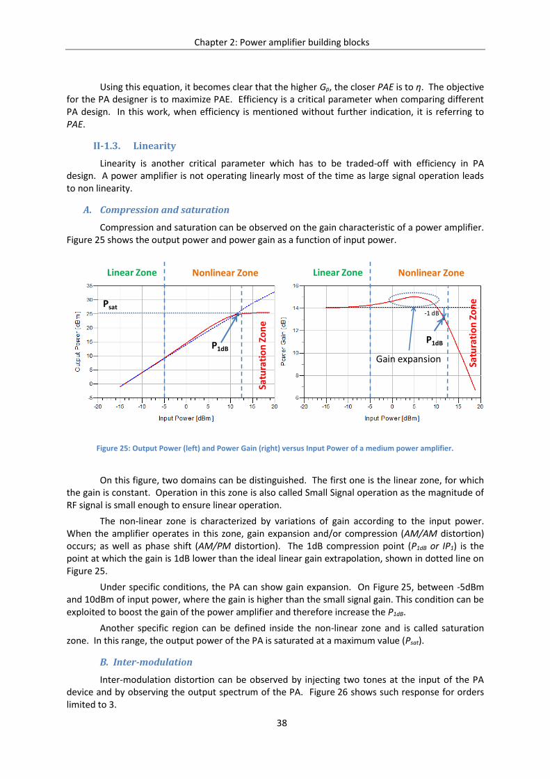
Compression and saturation can be observed on the gain characteristic of a power amplifier. Figure 25 shows the output power and power gain as a function of input power.
Figure 25: Output Power (left) and Power Gain (right) versus Input Power of a medium power amplifier.
On this figure, two domains can be distinguished. The first one is the linear zone, for which the gain is constant. Operation in this zone is also called Small Signal operation as the magnitude of RF signal is small enough to ensure linear operation.
The non-linear zone is characterized by variations of gain according to the input power. When the amplifier operates in this zone, gain expansion and/or compression (AM/AM distortion) occurs; as well as phase shift (AM/PM distortion). The 1dB compression point (P1dB or IP1) is the point at which the gain is 1dB lower than the ideal linear gain extrapolation, shown in dotted line on Figure 25.
Under specific conditions, the PA can show gain expansion. On Figure 25, between -5dBm and 10dBm of input power, where the gain is higher than the small signal gain. This condition can be exploited to boost the gain of the power amplifier and therefore increase the P1dB.
Another specific region can be defined inside the non-linear zone and is called saturation zone. In this range, the output power of the PA is saturated at a maximum value (Psat).
B. Inter-modulation
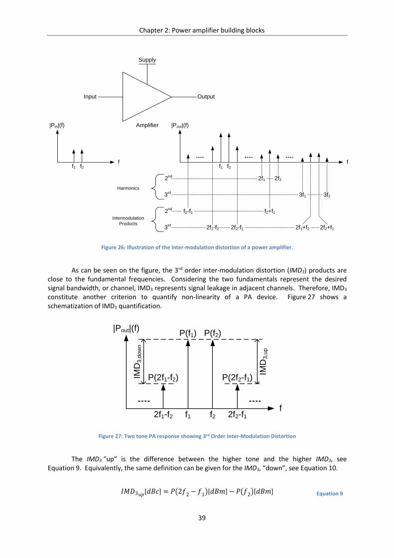
Inter-modulation distortion can be observed by injecting two tones at the input of the PA device and by observing the output spectrum of the PA. Figure 26 shows such response for orders limited to 3.
-1 dB
P1dBP1dB
Gain expansion
Linear Zone Nonlinear ZoneSa
tura
tio
n Z
on
e
Psat
Linear Zone Nonlinear Zone
Satu
rati
on
Zo
ne
Chapter 2: Power amplifier building blocks
39
Figure 26: Illustration of the inter-modulation distortion of a power amplifier.
As can be seen on the figure, the 3rd order inter-modulation distortion (IMD3) products are close to the fundamental frequencies. Considering the two fundamentals represent the desired signal bandwidth, or channel, IMD3 represents signal leakage in adjacent channels. Therefore, IMD3 constitute another criterion to quantify non-linearity of a PA device. Figure 27 shows a schematization of IMD3 quantification.
Figure 27: Two tone PA response showing 3rd Order Inter-Modulation Distortion
The IMD3 “up” is the difference between the higher tone and the higher IMD3, see Equation 9. Equivalently, the same definition can be given for the IMD3, “down”, see Equation 10.
𝐼𝑀𝐷3𝑢𝑝[𝑑𝐵𝑐] = 𝑃(2𝑓2 − 𝑓1)[𝑑𝐵𝑚]−𝑃(𝑓2)[𝑑𝐵𝑚] Equation 9
Amplifier
Supply
Input Output
|Pout|(f)
ff1 f2
2f1 2f2
3f1 3f2
Harmonics
2nd
3rd
Intermodulation
Products
2nd
3rd
f2-f1 f2+f1
2f2-f12f1-f2 2f2+f12f1+f2
|Pin|(f)
ff1 f2
|Pout|(f)
ff1 f2 2f2-f12f1-f2
P(f1) P(f2)
P(2f1-f2) P(2f2-f1)
IMD
3,u
p
IMD
3,d
ow
n
Chapter 2: Power amplifier building blocks
40
𝐼𝑀𝐷3𝑑𝑜𝑤𝑛[𝑑𝐵𝑐] = 𝑃(2𝑓1 − 𝑓2)[𝑑𝐵𝑚]−𝑃(𝑓1)[𝑑𝐵𝑚] Equation 10
It is worth noting that IMD3 may be asymmetric due to memory effects [Carvalho02]. One side may show a higher level of IMD3 than the other.
C. PA linearity under complex modulated signal
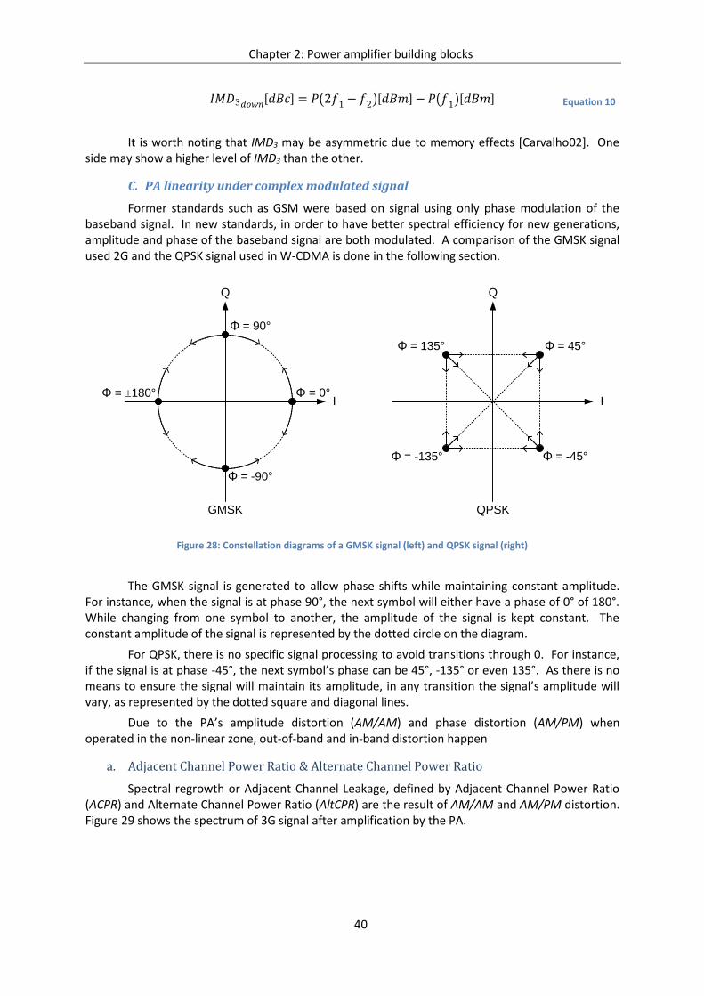
Former standards such as GSM were based on signal using only phase modulation of the baseband signal. In new standards, in order to have better spectral efficiency for new generations, amplitude and phase of the baseband signal are both modulated. A comparison of the GMSK signal used 2G and the QPSK signal used in W-CDMA is done in the following section.
Figure 28: Constellation diagrams of a GMSK signal (left) and QPSK signal (right)
The GMSK signal is generated to allow phase shifts while maintaining constant amplitude. For instance, when the signal is at phase 90°, the next symbol will either have a phase of 0° of 180°. While changing from one symbol to another, the amplitude of the signal is kept constant. The constant amplitude of the signal is represented by the dotted circle on the diagram.
For QPSK, there is no specific signal processing to avoid transitions through 0. For instance, if the signal is at phase -45°, the next symbol’s phase can be 45°, -135° or even 135°. As there is no means to ensure the signal will maintain its amplitude, in any transition the signal’s amplitude will vary, as represented by the dotted square and diagonal lines.
Due to the PA’s amplitude distortion (AM/AM) and phase distortion (AM/PM) when operated in the non-linear zone, out-of-band and in-band distortion happen
a. Adjacent Channel Power Ratio & Alternate Channel Power Ratio
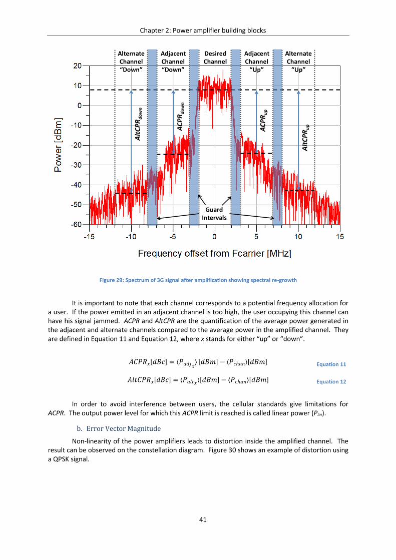
Spectral regrowth or Adjacent Channel Leakage, defined by Adjacent Channel Power Ratio (ACPR) and Alternate Channel Power Ratio (AltCPR) are the result of AM/AM and AM/PM distortion. Figure 29 shows the spectrum of 3G signal after amplification by the PA.
I
Q
QPSK
Φ = 135°
Φ = -135° Φ = -45°
Φ = 45°
I
Q
GMSK
Φ = 0°
Φ = 90°
Φ = ±180°
Φ = -90°
Chapter 2: Power amplifier building blocks
41
Figure 29: Spectrum of 3G signal after amplification showing spectral re-growth
It is important to note that each channel corresponds to a potential frequency allocation for a user. If the power emitted in an adjacent channel is too high, the user occupying this channel can have his signal jammed. ACPR and AltCPR are the quantification of the average power generated in the adjacent and alternate channels compared to the average power in the amplified channel. They are defined in Equation 11 and Equation 12, where x stands for either “up” or “down”.
𝐴𝐶𝑃𝑅𝑥[𝑑𝐵𝑐] = ⟨𝑃𝑎𝑑𝑗𝑥⟩ [𝑑𝐵𝑚]− ⟨𝑃𝑐ℎ𝑎𝑛⟩[𝑑𝐵𝑚] Equation 11
𝐴𝑙𝑡𝐶𝑃𝑅𝑥[𝑑𝐵𝑐] = ⟨𝑃𝑎𝑙𝑡𝑥⟩[𝑑𝐵𝑚]− ⟨𝑃𝑐ℎ𝑎𝑛⟩[𝑑𝐵𝑚] Equation 12
In order to avoid interference between users, the cellular standards give limitations for ACPR. The output power level for which this ACPR limit is reached is called linear power (Plin).
b. Error Vector Magnitude
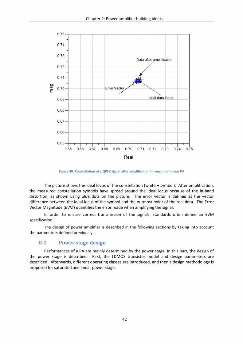
Non-linearity of the power amplifiers leads to distortion inside the amplified channel. The result can be observed on the constellation diagram. Figure 30 shows an example of distortion using a QPSK signal.
DesiredChannel
AdjacentChannel
“Up”
AlternateChannel
“Up”
AdjacentChannel“Down”
AlternateChannel“Down”
AC
PR
up
AC
PR
do
wn
Alt
CP
Ru
p
Alt
CP
Rd
ow
n
GuardIntervals
Chapter 2: Power amplifier building blocks
42
Figure 30: Constellation of a QPSK signal after amplification through non-linear PA
The picture shows the ideal locus of the constellation (white + symbol). After amplification, the measured constellation symbols have spread around the ideal locus because of the in-band distortion, as shown using blue dots on the picture. The error vector is defined as the vector difference between the ideal locus of the symbol and the outmost point of the real data. The Error Vector Magnitude (EVM) quantifies the error made when amplifying the signal.
In order to ensure correct transmission of the signals, standards often define an EVM specification.
The design of power amplifier is described in the following sections by taking into account the parameters defined previously.
II-2 Power stage design
Performances of a PA are mainly determined by the power stage. In this part, the design of the power stage is described. First, the LDMOS transistor model and design parameters are described. Afterwards, different operating classes are introduced, and then a design methodology is proposed for saturated and linear power stage.
+
Data after amplification
Ideal data locus
Error Vector
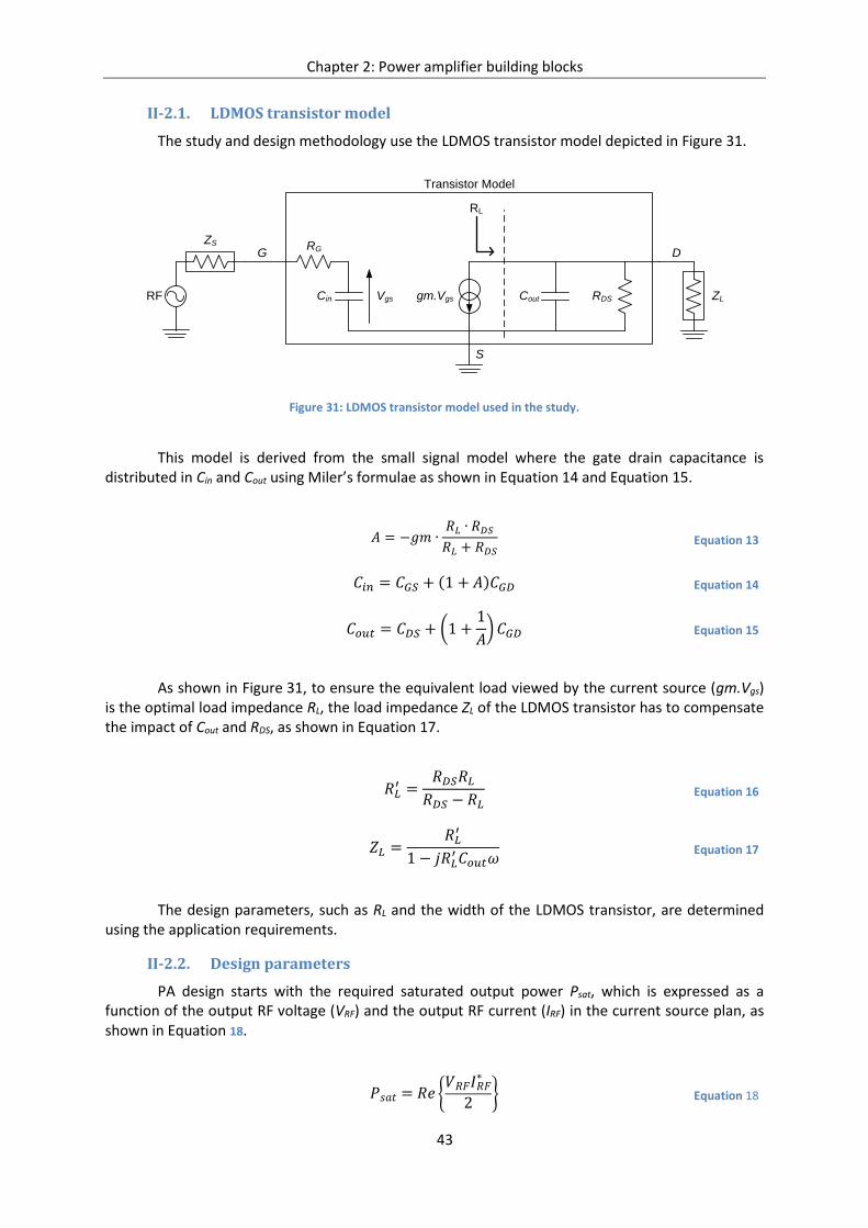
Chapter 2: Power amplifier building blocks
43
II-2.1. LDMOS transistor model
The study and design methodology use the LDMOS transistor model depicted in Figure 31.
Figure 31: LDMOS transistor model used in the study.
This model is derived from the small signal model where the gate drain capacitance is distributed in Cin and Cout using Miler’s formulae as shown in Equation 14 and Equation 15.
𝐴 = −𝑔𝑚 ∙𝑅𝐿 ∙ 𝑅𝐷𝑆𝑅𝐿 + 𝑅𝐷𝑆
Equation 13
𝐶𝑖𝑛 = 𝐶𝐺𝑆 + (1 + 𝐴)𝐶𝐺𝐷 Equation 14
𝐶𝑜𝑢𝑡 = 𝐶𝐷𝑆 + (1 +1
𝐴)𝐶𝐺𝐷 Equation 15
As shown in Figure 31, to ensure the equivalent load viewed by the current source (gm.Vgs) is the optimal load impedance RL, the load impedance ZL of the LDMOS transistor has to compensate the impact of Cout and RDS, as shown in Equation 17.
𝑅𝐿′ =
𝑅𝐷𝑆𝑅𝐿𝑅𝐷𝑆 − 𝑅𝐿
Equation 16
𝑍𝐿 =𝑅𝐿′
1 − 𝑗𝑅𝐿′𝐶𝑜𝑢𝑡𝜔
Equation 17
The design parameters, such as RL and the width of the LDMOS transistor, are determined using the application requirements.
II-2.2. Design parameters
PA design starts with the required saturated output power Psat, which is expressed as a function of the output RF voltage (VRF) and the output RF current (IRF) in the current source plan, as shown in Equation 18.
𝑃𝑠𝑎𝑡 = 𝑅𝑒 𝑉𝑅𝐹𝐼𝑅𝐹
∗
2 Equation 18
RF Vgs gm.VgsCin Cout
RG
ZL
Transistor Model
ZS
RDS
G D
S
RL

Chapter 2: Power amplifier building blocks
44
The optimal load resistance to present to the current source of the LDMOS transistor is determined with Equation 19.
𝑅𝐿𝑜𝑝𝑡 =𝑉𝑅𝐹𝐼𝑅𝐹
Equation 19
From this expression, the optimal load of the LDMOS transistor can be rewritten as Equation 20.
𝑅𝐿𝑜𝑝𝑡 =(𝑚𝑎𝑔𝑉𝑅𝐹)
2
2𝑃𝑠𝑎𝑡 Equation 20
Finally, the efficiency of the device at the saturation is calculated thanks to Psat and PDC (see Equation 21) where Idq is the quiescent DC current of the device and VDD the supply voltage. The final efficiency expression is given in Equation 22.
𝑃𝐷𝐶 = 𝑉𝐷𝐷𝐼𝑑𝑞 Equation 21
𝜂 =𝑃𝑠𝑎𝑡𝑃𝐷𝐶
=𝑅𝑒𝑉𝑅𝐹𝐼𝑅𝐹
∗
2𝑉𝐷𝐷𝐼𝑑𝑞 Equation 22
The RF voltage is limited by the load line of the LDMOS transistor and the Ids/Vds characteristic of the LDMOS transistor, as shown in Figure 32.
Figure 32: Linearized IDS vs.VDS characteristic (solid lines) and load line (dotted line) of a common source LDMOS transistor.
k
DD
V
V
2 DD k
DD
V V
V
Incre
asin
g V
GG
VDS sat
Loci
Ohmic Region Saturated Region
Output Voltage Dynamic
Class A Loadline
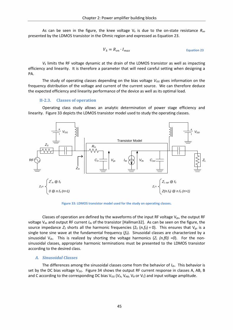
Chapter 2: Power amplifier building blocks
45
As can be seen in the figure, the knee voltage Vk is due to the on-state resistance Ron presented by the LDMOS transistor in the Ohmic region and expressed as Equation 23.
𝑉𝑘 = 𝑅𝑜𝑛 ∙ 𝐼𝑚𝑎𝑥 Equation 23
Vk limits the RF voltage dynamic at the drain of the LDMOS transistor as well as impacting efficiency and linearity. It is therefore a parameter that will need careful setting when designing a PA.
The study of operating classes depending on the bias voltage VGG gives information on the frequency distribution of the voltage and current of the current source. We can therefore deduce the expected efficiency and linearity performance of the device as well as its optimal load.
II-2.3. Classes of operation
Operating class study allows an analytic determination of power stage efficiency and linearity. Figure 33 depicts the LDMOS transistor model used to study the operating classes.
Figure 33: LDMOS transistor model used for the study on operating classes.
Classes of operation are defined by the waveforms of the input RF voltage Vgs, the output RF voltage Vds and output RF current Ids of the transistor [Hallman32]. As can be seen on the figure, the source impedance ZS shorts all the harmonic frequencies (ZS (n.f0) = 0). This ensures that Vgs is a single tone sine wave at the fundamental frequency (f0). Sinusoidal classes are characterized by a sinusoidal Vds. This is realized by shorting the voltage harmonics (ZL (n.f0) =0). For the non-sinusoidal classes, appropriate harmonic terminations must be presented to the LDMOS transistor according to the desired class.
A. Sinusoidal Classes
The differences among the sinusoidal classes come from the behavior of Ids. This behavior is set by the DC bias voltage VGG. Figure 34 shows the output RF current response in classes A, AB, B and C according to the corresponding DC bias VGG (VA, VAB, VB or VC) and input voltage amplitude.
RF Vgs Ids VdsCin Cout
RG
ZL
Transistor Model
ZS
VGG
Zin
0 @ n.f0 (n>1)
Z*in @ f0
ZS=
Z(n.f0) @ n.f0 (n>1)
ZL opt @ f0
ZL=
VDD
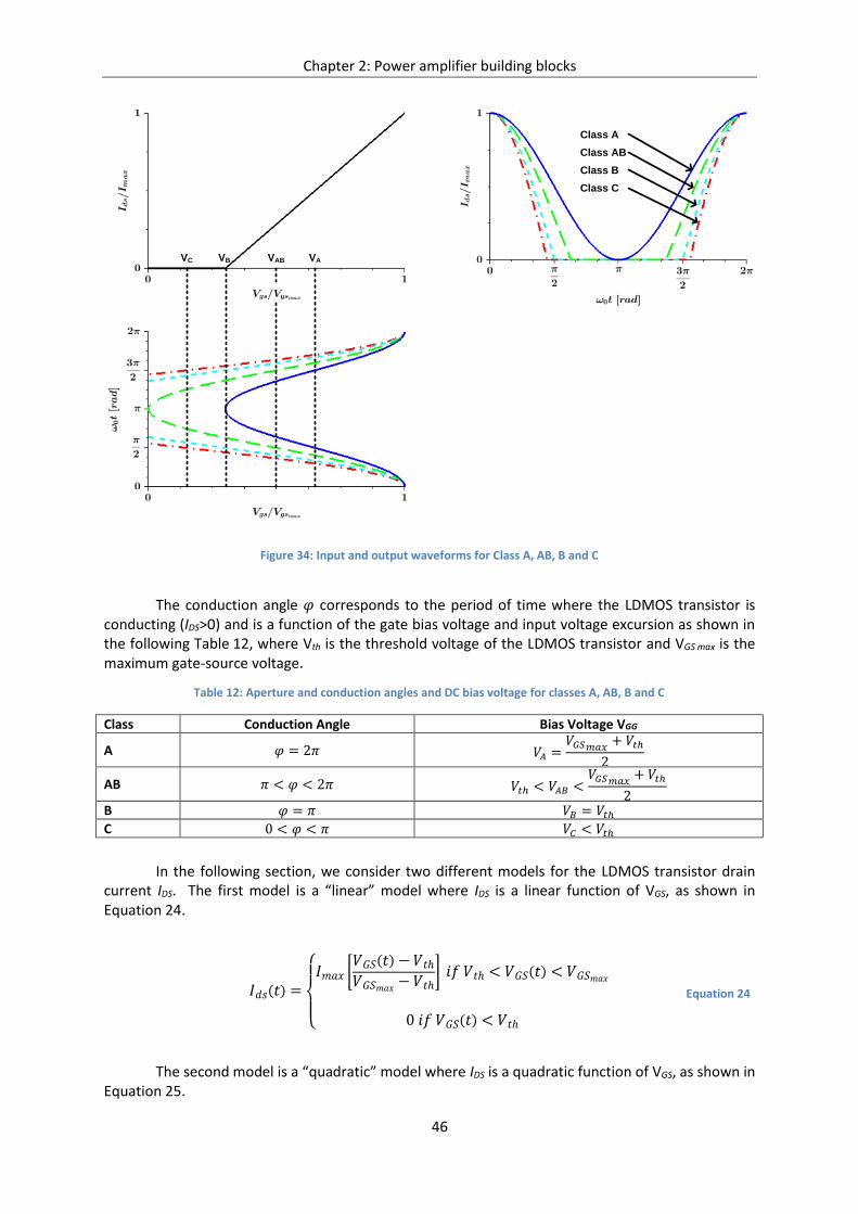
Chapter 2: Power amplifier building blocks
46
Figure 34: Input and output waveforms for Class A, AB, B and C
The conduction angle 𝜑 corresponds to the period of time where the LDMOS transistor is conducting (IDS>0) and is a function of the gate bias voltage and input voltage excursion as shown in the following Table 12, where Vth is the threshold voltage of the LDMOS transistor and VGS max is the maximum gate-source voltage.
Table 12: Aperture and conduction angles and DC bias voltage for classes A, AB, B and C
Class Conduction Angle Bias Voltage VGG
A 𝜑 = 2𝜋 𝑉𝐴 =𝑉𝐺𝑆𝑚𝑎𝑥 + 𝑉𝑡ℎ
2
AB 𝜋 < 𝜑 < 2𝜋 𝑉𝑡ℎ < 𝑉𝐴𝐵 <𝑉𝐺𝑆𝑚𝑎𝑥 + 𝑉𝑡ℎ
2
B 𝜑 = 𝜋 𝑉𝐵 = 𝑉𝑡ℎ
C 0 < 𝜑 < 𝜋 𝑉𝐶 < 𝑉𝑡ℎ
In the following section, we consider two different models for the LDMOS transistor drain current IDS. The first model is a “linear” model where IDS is a linear function of VGS, as shown in Equation 24.
𝐼𝑑𝑠(𝑡) =
𝐼𝑚𝑎𝑥 [
𝑉𝐺𝑆(𝑡)−𝑉𝑡ℎ𝑉𝐺𝑆𝑚𝑎𝑥 −𝑉𝑡ℎ
] 𝑖𝑓 𝑉𝑡ℎ < 𝑉𝐺𝑆(𝑡) < 𝑉𝐺𝑆𝑚𝑎𝑥
0 𝑖𝑓 𝑉𝐺𝑆(𝑡) < 𝑉𝑡ℎ
Equation 24
The second model is a “quadratic” model where IDS is a quadratic function of VGS, as shown in Equation 25.
VAVABVBVC
Class A
Class AB
Class B
Class C
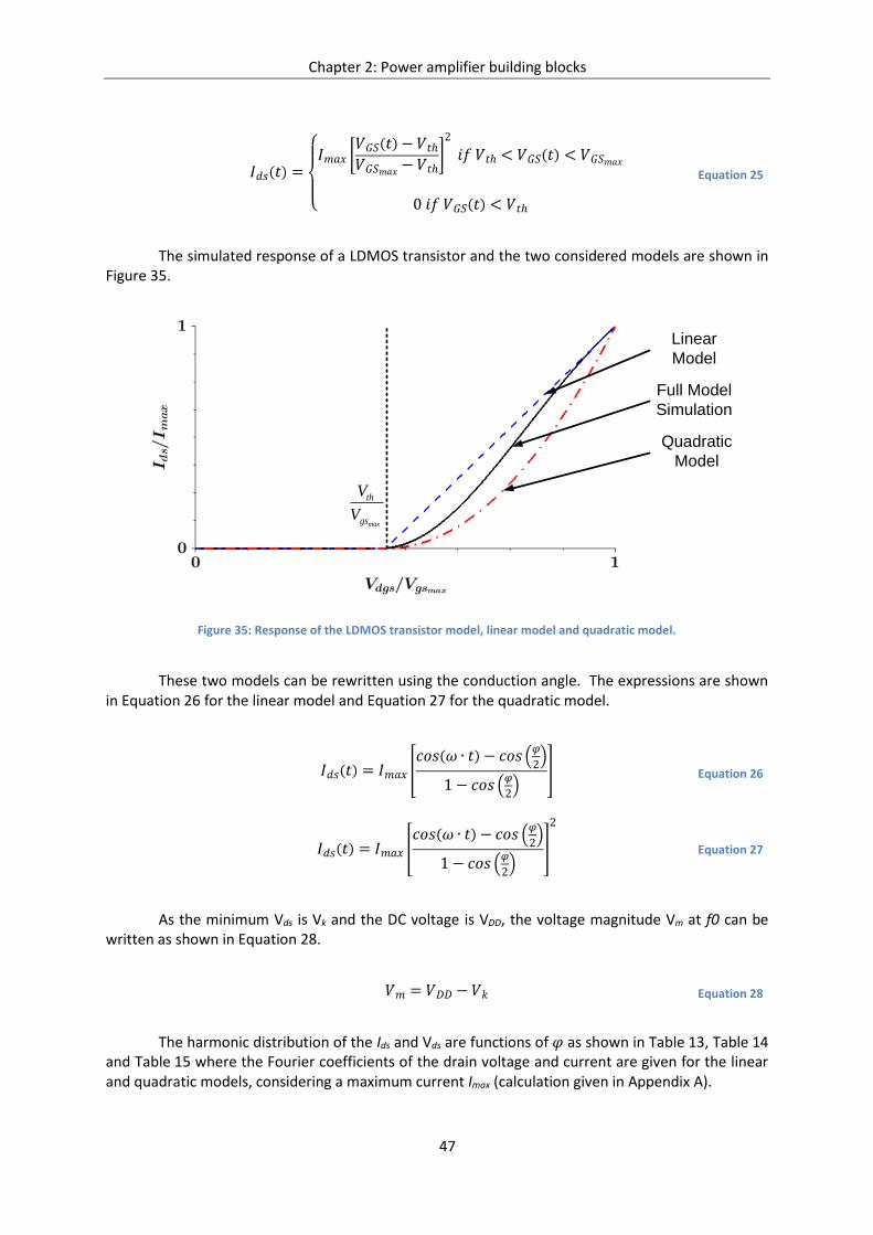
Chapter 2: Power amplifier building blocks
47
𝐼𝑑𝑠(𝑡) =
𝐼𝑚𝑎𝑥 [
𝑉𝐺𝑆(𝑡)−𝑉𝑡ℎ𝑉𝐺𝑆𝑚𝑎𝑥 −𝑉𝑡ℎ
]
2
𝑖𝑓 𝑉𝑡ℎ < 𝑉𝐺𝑆(𝑡) < 𝑉𝐺𝑆𝑚𝑎𝑥
0 𝑖𝑓 𝑉𝐺𝑆(𝑡) < 𝑉𝑡ℎ
Equation 25
The simulated response of a LDMOS transistor and the two considered models are shown in Figure 35.
Figure 35: Response of the LDMOS transistor model, linear model and quadratic model.
These two models can be rewritten using the conduction angle. The expressions are shown in Equation 26 for the linear model and Equation 27 for the quadratic model.
𝐼𝑑𝑠(𝑡) = 𝐼𝑚𝑎𝑥 [𝑐𝑜𝑠(𝜔 ∙ 𝑡)− 𝑐𝑜𝑠 (
𝜑
2)
1 − 𝑐𝑜𝑠 (𝜑
2)
] Equation 26
𝐼𝑑𝑠(𝑡) = 𝐼𝑚𝑎𝑥 [𝑐𝑜𝑠(𝜔 ∙ 𝑡)− 𝑐𝑜𝑠 (
𝜑
2)
1 − 𝑐𝑜𝑠 (𝜑
2)
]
2
Equation 27
As the minimum Vds is Vk and the DC voltage is VDD, the voltage magnitude Vm at f0 can be written as shown in Equation 28.
𝑉𝑚 = 𝑉𝐷𝐷 −𝑉𝑘 Equation 28
The harmonic distribution of the Ids and Vds are functions of 𝜑 as shown in Table 13, Table 14 and Table 15 where the Fourier coefficients of the drain voltage and current are given for the linear and quadratic models, considering a maximum current Imax (calculation given in Appendix A).
max
th
gs
V
V
Full Model
Simulation
Quadratic
Model
Linear
Model
Chapter 2: Power amplifier building blocks
48
Table 13: DC components of each signals
Signal DC coefficient
Voltage Vds[0] 𝑉𝐷𝐷
Current Ids[0] (Linear model)
𝐼𝑚𝑎𝑥𝜋
∙ [sin (
𝜑
2) −
𝜑
2cos (
𝜑
2)
1 − cos (𝜑
2)
]
Current Ids [0] (Quadratic model)
𝐼𝑚𝑎𝑥𝜋
∙1
(1 − cos (𝜑
2))
2 ∙ [𝜑
2+𝜑
4cos(𝜑) −
3
4sin(𝜑)]
Table 14: Fundamental components of each signals
Signal Fundamental coefficient
Voltage Vds [f0] 𝑉𝑚 = 𝑉𝐷𝐷 − 𝑉𝑘
Current Ids [f0] (Linear model)
𝐼𝑚𝑎𝑥2𝜋
∙ [𝜑 − sin(𝜑)
1 − cos (𝜑
2)]
Current Ids [f0] (Quadratic model)
2𝐼𝑚𝑎𝑥𝜋
∙1
(1 − cos (𝜑
2))
2 ∙ [3
4sin (
𝜑
2) −
𝜑
2cos (
𝜑
2) +
1
12sin (
3𝜑
2)]
Table 15: Harmonic components of each signals
Signal DC coefficient
Voltage Vds[n.f0] 0
Current Ids[n.f0] (Linear model)
𝐼𝑚𝑎𝑥𝜋
∙1
1 − cos (𝜑
2)∙ [sin ((n + 1)
𝜑
2)
n + 1+sin ((n − 1)
𝜑
2)
n − 1]
Current Ids[n.f0] (Quadratic model)
2𝐼𝑚𝑎𝑥𝜋
∙1
(1 − cos (𝜑
2))
2 ∙ (𝜑
8−1
6sin(𝜑) +
1
48sin(2𝜑)) for 𝑛 = 2
2𝐼𝑚𝑎𝑥𝜋
∙1
(1 − cos (𝜑
2))
2 ∙(4 − 𝑛2) sin (𝑛
𝜑
2) + (𝑛 − 1)(𝑛 − 2) sin (𝑛
𝜑
2) cos(𝜑) + 3𝑛 sin ((𝑛 − 2)
𝜑
2)
𝑛(𝑛2 − 1)(𝑛2 − 4)
Expressions of the RF output power (PRF) and DC power (PDC) are given by Equation 29 and Equation 30.
𝑃𝑅𝐹 =𝑘𝑖1 ∙ 𝐼𝑚𝑎𝑥 ∙ (𝑉𝐷𝐷 −𝑉𝑘)
2 Equation 29
𝑃𝐷𝐶 = 𝑘𝑖0 ∙ 𝐼𝑚𝑎𝑥 ∙ 𝑉𝐷𝐷 Equation 30
Where
𝑘𝑖0 =𝐼𝑑𝑠[0]
𝐼𝑚𝑎𝑥 Equation 31
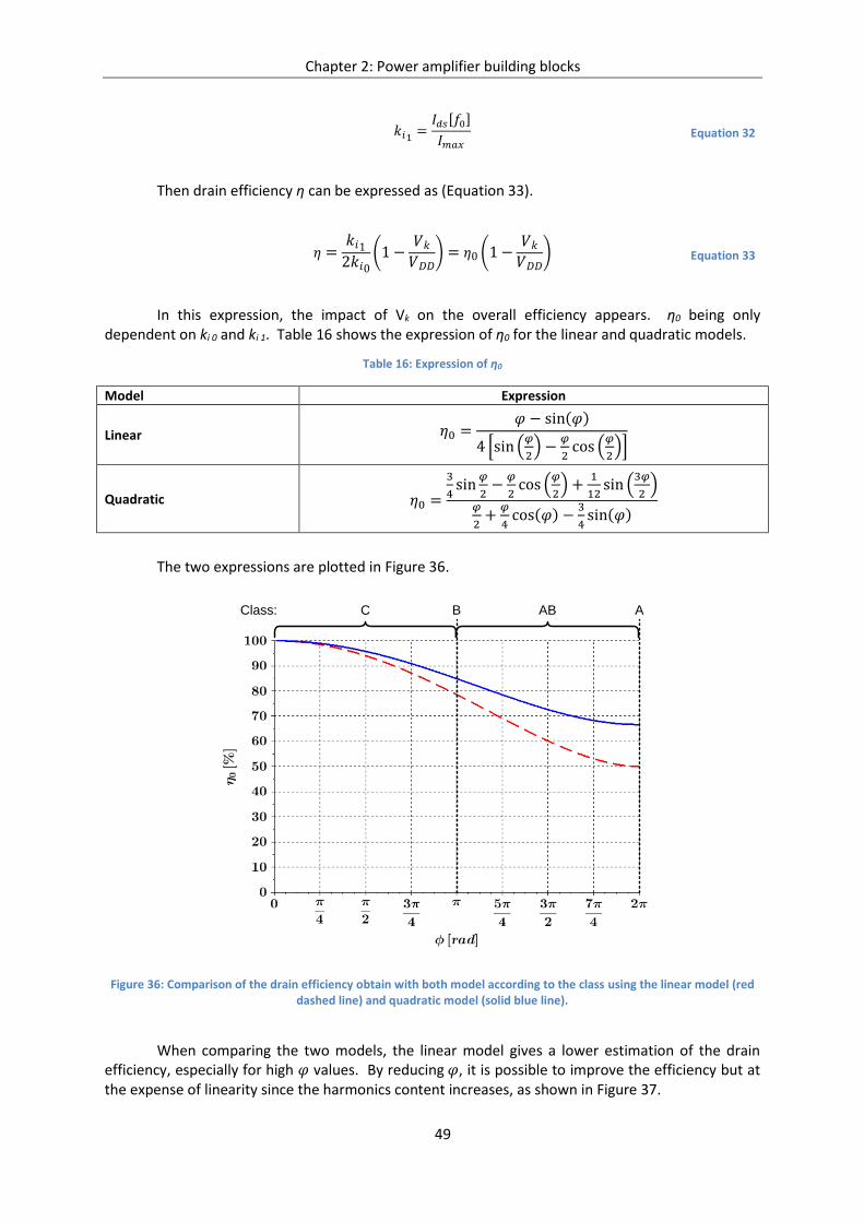
Chapter 2: Power amplifier building blocks
49
𝑘𝑖1 =𝐼𝑑𝑠[𝑓0]
𝐼𝑚𝑎𝑥 Equation 32
Then drain efficiency η can be expressed as (Equation 33).
𝜂 =𝑘𝑖12𝑘𝑖0
(1 −𝑉𝑘𝑉𝐷𝐷
) = 𝜂0 (1 −𝑉𝑘𝑉𝐷𝐷
) Equation 33
In this expression, the impact of Vk on the overall efficiency appears. η0 being only dependent on ki 0 and ki 1. Table 16 shows the expression of η0 for the linear and quadratic models.
Table 16: Expression of η0
Model Expression
Linear 𝜂0 =𝜑 − sin(𝜑)
4 [sin (𝜑
2) −
𝜑
2cos (
𝜑
2)]
Quadratic 𝜂0 =
3
4sin
𝜑
2−𝜑
2cos (
𝜑
2) +
1
12sin (
3𝜑
2)
𝜑
2+𝜑
4cos(𝜑) −
3
4sin(𝜑)
The two expressions are plotted in Figure 36.
Figure 36: Comparison of the drain efficiency obtain with both model according to the class using the linear model (red dashed line) and quadratic model (solid blue line).
When comparing the two models, the linear model gives a lower estimation of the drain efficiency, especially for high 𝜑 values. By reducing 𝜑, it is possible to improve the efficiency but at the expense of linearity since the harmonics content increases, as shown in Figure 37.
C ABClass: AB
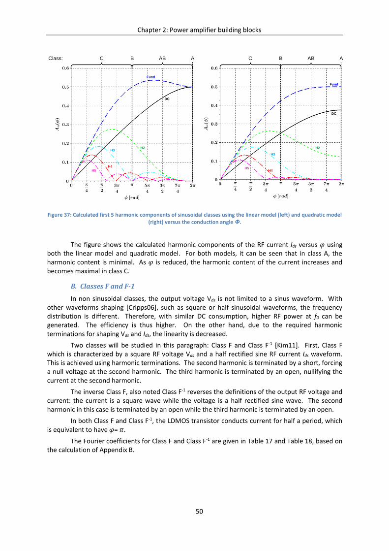
Chapter 2: Power amplifier building blocks
50
Figure 37: Calculated first 5 harmonic components of sinusoidal classes using the linear model (left) and quadratic model (right) versus the conduction angle Φ.
The figure shows the calculated harmonic components of the RF current Ids versus 𝜑 using both the linear model and quadratic model. For both models, it can be seen that in class A, the harmonic content is minimal. As 𝜑 is reduced, the harmonic content of the current increases and becomes maximal in class C.
B. Classes F and F-1
In non sinusoidal classes, the output voltage Vds is not limited to a sinus waveform. With other waveforms shaping [Cripps06], such as square or half sinusoidal waveforms, the frequency distribution is different. Therefore, with similar DC consumption, higher RF power at f0 can be generated. The efficiency is thus higher. On the other hand, due to the required harmonic terminations for shaping Vds and Ids, the linearity is decreased.
Two classes will be studied in this paragraph: Class F and Class F-1 [Kim11]. First, Class F which is characterized by a square RF voltage Vds and a half rectified sine RF current Ids waveform. This is achieved using harmonic terminations. The second harmonic is terminated by a short, forcing a null voltage at the second harmonic. The third harmonic is terminated by an open, nullifying the current at the second harmonic.
The inverse Class F, also noted Class F-1 reverses the definitions of the output RF voltage and current: the current is a square wave while the voltage is a half rectified sine wave. The second harmonic in this case is terminated by an open while the third harmonic is terminated by an open.
In both Class F and Class F-1, the LDMOS transistor conducts current for half a period, which is equivalent to have 𝜑= 𝜋.
The Fourier coefficients for Class F and Class F-1 are given in Table 17 and Table 18, based on the calculation of Appendix B.
DC
Fund
H2H3
H4
H5
DC
Fund
H2
H3
H4H5
C ABClass: AB C AB AB
Chapter 2: Power amplifier building blocks
51
Table 17: DC components of voltage and current in Class F and Class F-1
Signal DC coefficient in Class F DC coefficient in Class F-1
Voltage Vds[0] 𝑉𝐷𝐷 𝑉𝐷𝐷
Current Ids[0] 𝐼𝑚𝑎𝑥𝜋
𝐼𝑚𝑎𝑥2
Table 18: Fundamental components of voltage and current in Class F and Class F-1
Signal Fundamental coefficient in Class F Fundamental coefficient in Class F-1
Voltage Vds [f0] 4
𝜋(𝑉𝐷𝐷 − 𝑉𝑘) =
4𝑉𝑚𝜋
𝜋
2(𝑉𝐷𝐷 − 𝑉𝑘) =
𝜋𝑉𝑚2
Current Ids [f0] 𝐼𝑚𝑎𝑥2
2𝐼𝑚𝑎𝑥𝜋
Using those coefficients, it is possible to determine the fundamental distribution coefficient kv 1 for the fundamental frequency of the voltage RF signal, see Equation 34. Similarly, DC current and fundamental distribution coefficients can be expressed as Equation 35 and Equation 36.
𝑘𝑣1 =𝑉𝑑𝑠(𝑓0)
(𝑉𝐷𝐷 −𝑉𝑘)=𝑉𝑑𝑠(𝑓0)
𝑉𝑚 Equation 34
𝑘𝑖0 =𝐼(𝐷𝐶)
𝐼𝑚𝑎𝑥 Equation 35
𝑘𝑖1 =𝐼(𝑓0)
𝐼𝑚𝑎𝑥 Equation 36
Using those coefficients it is possible to write the drain efficiency as follows in Equation 37.
𝜂 =𝑘𝑖1 ∙ 𝑘𝑣12𝑘𝑖0
(1 −𝑉𝑘𝑉𝐷𝐷
) = 𝜂0 (1 −𝑉𝑘𝑉𝐷𝐷
) Equation 37
By casting the impact of Vk aside, we can calculate η0 in each class, see Table 19.
Table 19: Exact and approximated η0 for classes deep AB, F and F-1, for each current model
Operation Class Deep Class AB Class F Class F-1
Value Exact Approximation Exact Approximation Exact Approximation
Linear Model 𝜋
4 79%
1 100% 1 100%
Quadratic Model 8
3𝜋 85%
This table shows that using either class F or F-1, the ideal drain efficiency of the power stage can be risen to 100% for the same conduction time. This means using different spectral distribution of the signals allows higher efficiency for a degraded linearity due to the waveforms.
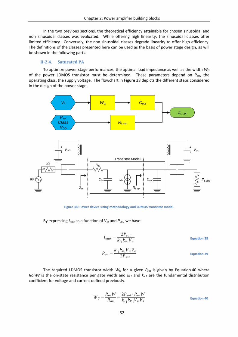
Chapter 2: Power amplifier building blocks
52
In the two previous sections, the theoretical efficiency attainable for chosen sinusoidal and non sinusoidal classes was evaluated. While offering high linearity, the sinusoidal classes offer limited efficiency. Conversely, the non sinusoidal classes degrade linearity to offer high efficiency. The definitions of the classes presented here can be used as the basis of power stage design, as will be shown in the following parts.
II-2.4. Saturated PA
To optimize power stage performances, the optimal load impedance as well as the width WG of the power LDMOS transistor must be determined. These parameters depend on Psat, the operating class, the supply voltage. The flowchart in Figure 38 depicts the different steps considered in the design of the power stage.
Figure 38: Power device sizing methodology and LDMOS transistor model.
By expressing Imax as a function of Vm and Psat, we have:
𝐼𝑚𝑎𝑥 =2𝑃𝑠𝑎𝑡
𝑘𝑖1𝑘𝑣1𝑉𝑚 Equation 38
𝑅𝑜𝑛 =𝑘𝑖1𝑘𝑣1𝑉𝑚𝑉𝑘
2𝑃𝑠𝑎𝑡 Equation 39
The required LDMOS transistor width WG for a given Psat is given by Equation 40 where RonW is the on-state resistance per gate width and ki 1 and kv 1 are the fundamental distribution coefficient for voltage and current defined previously.
𝑊𝐺 =𝑅𝑜𝑛𝑊
𝑅𝑜𝑛=2𝑃𝑠𝑎𝑡 ∙ 𝑅𝑜𝑛𝑊
𝑘𝐼1𝑘𝑉1𝑉𝑚𝑉𝑘 Equation 40
Psat
Class
VDD
Vk
RL opt
WG Cout
ZL opt
RF IdsCin Cout
RG
ZL opt
Transistor Model
ZS
VGG
Zin
VDD
RL opt
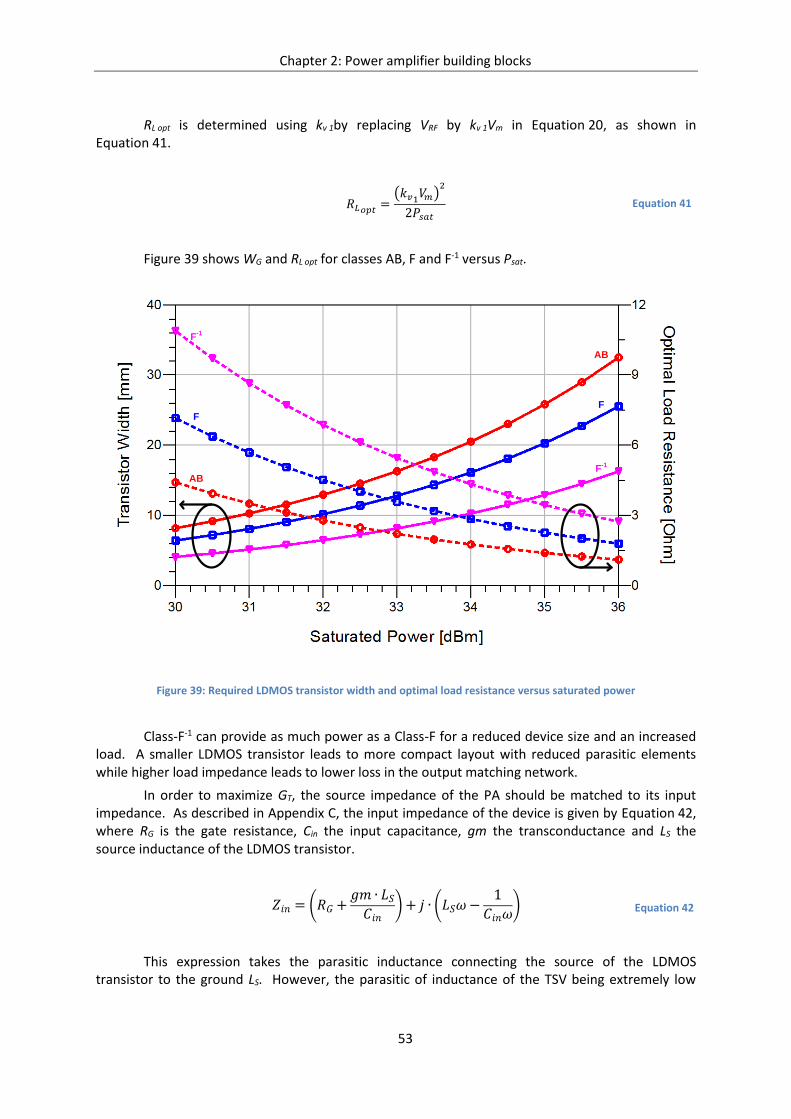
Chapter 2: Power amplifier building blocks
53
RL opt is determined using kv 1by replacing VRF by kv 1Vm in Equation 20, as shown in Equation 41.
𝑅𝐿𝑜𝑝𝑡 =(𝑘𝑣1𝑉𝑚)
2
2𝑃𝑠𝑎𝑡 Equation 41
Figure 39 shows WG and RL opt for classes AB, F and F-1 versus Psat.
Figure 39: Required LDMOS transistor width and optimal load resistance versus saturated power
Class-F-1 can provide as much power as a Class-F for a reduced device size and an increased load. A smaller LDMOS transistor leads to more compact layout with reduced parasitic elements while higher load impedance leads to lower loss in the output matching network.
In order to maximize GT, the source impedance of the PA should be matched to its input impedance. As described in Appendix C, the input impedance of the device is given by Equation 42, where RG is the gate resistance, Cin the input capacitance, gm the transconductance and LS the source inductance of the LDMOS transistor.
𝑍𝑖𝑛 = (𝑅𝐺 +𝑔𝑚 ∙ 𝐿𝑆𝐶𝑖𝑛
)+ 𝑗 ∙ (𝐿𝑆𝜔−1
𝐶𝑖𝑛𝜔) Equation 42
This expression takes the parasitic inductance connecting the source of the LDMOS transistor to the ground LS. However, the parasitic of inductance of the TSV being extremely low
AB
AB
F-1
F-1
F
F
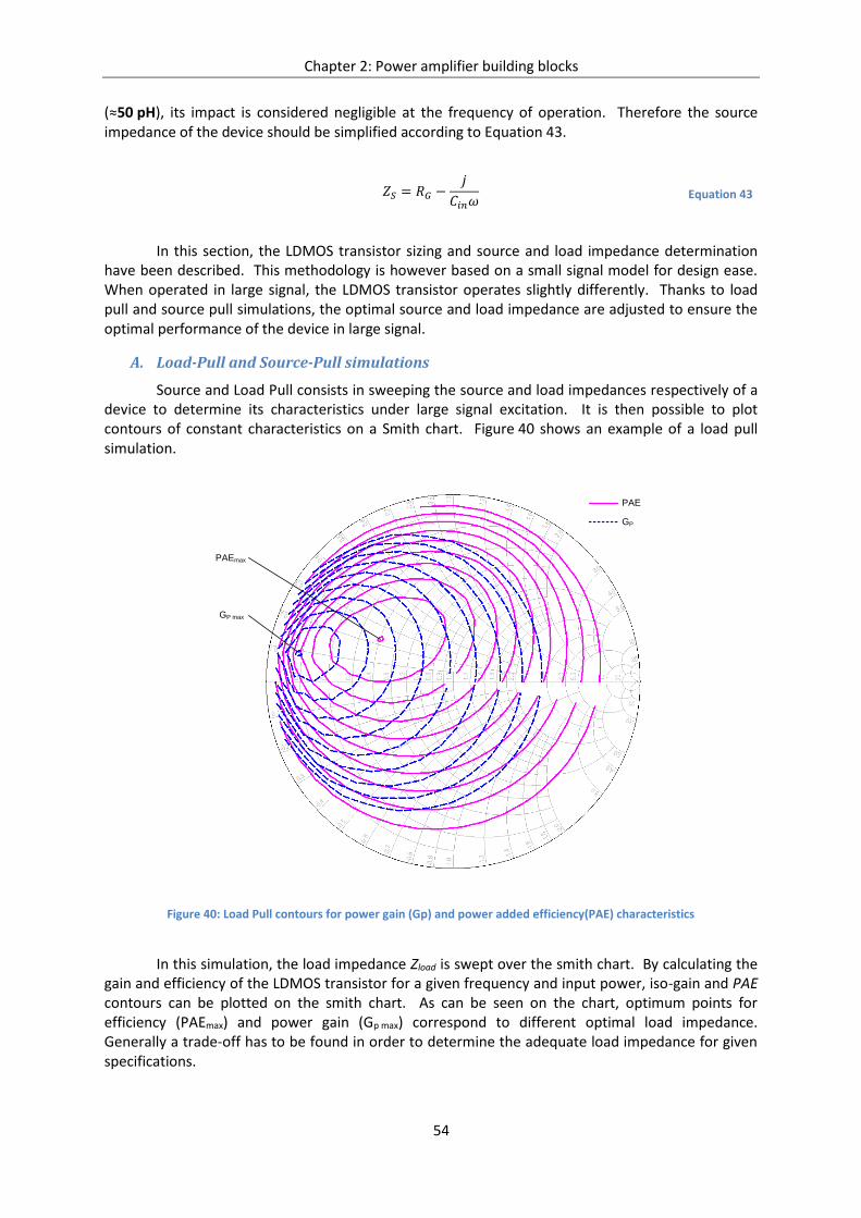
Chapter 2: Power amplifier building blocks
54
(≈50 pH), its impact is considered negligible at the frequency of operation. Therefore the source impedance of the device should be simplified according to Equation 43.
𝑍𝑆 = 𝑅𝐺 −𝑗
𝐶𝑖𝑛𝜔 Equation 43
In this section, the LDMOS transistor sizing and source and load impedance determination have been described. This methodology is however based on a small signal model for design ease. When operated in large signal, the LDMOS transistor operates slightly differently. Thanks to load pull and source pull simulations, the optimal source and load impedance are adjusted to ensure the optimal performance of the device in large signal.
A. Load-Pull and Source-Pull simulations
Source and Load Pull consists in sweeping the source and load impedances respectively of a device to determine its characteristics under large signal excitation. It is then possible to plot contours of constant characteristics on a Smith chart. Figure 40 shows an example of a load pull simulation.
Figure 40: Load Pull contours for power gain (Gp) and power added efficiency(PAE) characteristics
In this simulation, the load impedance Zload is swept over the smith chart. By calculating the gain and efficiency of the LDMOS transistor for a given frequency and input power, iso-gain and PAE contours can be plotted on the smith chart. As can be seen on the chart, optimum points for efficiency (PAEmax) and power gain (Gp max) correspond to different optimal load impedance. Generally a trade-off has to be found in order to determine the adequate load impedance for given specifications.
PAE
GP
PAEmax
GP max
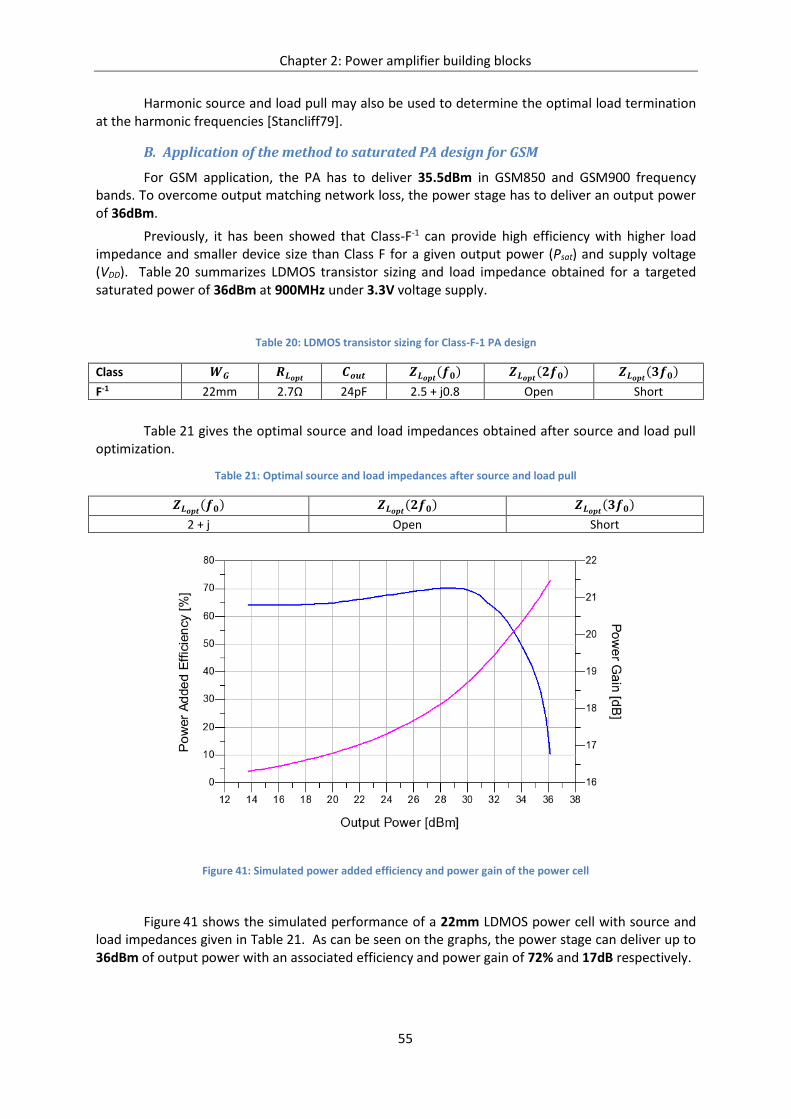
Chapter 2: Power amplifier building blocks
55
Harmonic source and load pull may also be used to determine the optimal load termination at the harmonic frequencies [Stancliff79].
B. Application of the method to saturated PA design for GSM
For GSM application, the PA has to deliver 35.5dBm in GSM850 and GSM900 frequency bands. To overcome output matching network loss, the power stage has to deliver an output power of 36dBm.
Previously, it has been showed that Class-F-1 can provide high efficiency with higher load impedance and smaller device size than Class F for a given output power (Psat) and supply voltage (VDD). Table 20 summarizes LDMOS transistor sizing and load impedance obtained for a targeted saturated power of 36dBm at 900MHz under 3.3V voltage supply.
Table 20: LDMOS transistor sizing for Class-F-1 PA design
Class 𝑾𝑮 𝑹𝑳𝒐𝒑𝒕 𝑪𝒐𝒖𝒕 𝒁𝑳𝒐𝒑𝒕(𝒇𝟎) 𝒁𝑳𝒐𝒑𝒕(𝟐𝒇𝟎) 𝒁𝑳𝒐𝒑𝒕(𝟑𝒇𝟎)
F-1 22mm 2.7Ω 24pF 2.5 + j0.8 Open Short
Table 21 gives the optimal source and load impedances obtained after source and load pull optimization.
Table 21: Optimal source and load impedances after source and load pull
𝒁𝑳𝒐𝒑𝒕(𝒇𝟎) 𝒁𝑳𝒐𝒑𝒕(𝟐𝒇𝟎) 𝒁𝑳𝒐𝒑𝒕(𝟑𝒇𝟎)
2 + j Open Short
Figure 41: Simulated power added efficiency and power gain of the power cell
Figure 41 shows the simulated performance of a 22mm LDMOS power cell with source and load impedances given in Table 21. As can be seen on the graphs, the power stage can deliver up to 36dBm of output power with an associated efficiency and power gain of 72% and 17dB respectively.
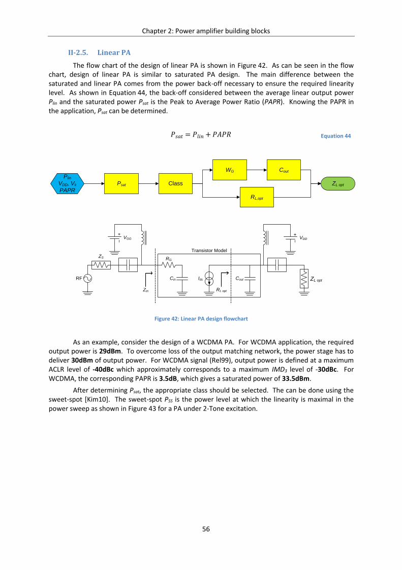
Chapter 2: Power amplifier building blocks
56
II-2.5. Linear PA
The flow chart of the design of linear PA is shown in Figure 42. As can be seen in the flow chart, design of linear PA is similar to saturated PA design. The main difference between the saturated and linear PA comes from the power back-off necessary to ensure the required linearity level. As shown in Equation 44, the back-off considered between the average linear output power Plin and the saturated power Psat is the Peak to Average Power Ratio (PAPR). Knowing the PAPR in the application, Psat can be determined.
𝑃𝑠𝑎𝑡 = 𝑃𝑙𝑖𝑛 +𝑃𝐴𝑃𝑅 Equation 44
Figure 42: Linear PA design flowchart
As an example, consider the design of a WCDMA PA. For WCDMA application, the required output power is 29dBm. To overcome loss of the output matching network, the power stage has to deliver 30dBm of output power. For WCDMA signal (Rel99), output power is defined at a maximum ACLR level of -40dBc which approximately corresponds to a maximum IMD3 level of -30dBc. For WCDMA, the corresponding PAPR is 3.5dB, which gives a saturated power of 33.5dBm.
After determining Psat, the appropriate class should be selected. The can be done using the sweet-spot [Kim10]. The sweet-spot PSS is the power level at which the linearity is maximal in the power sweep as shown in Figure 43 for a PA under 2-Tone excitation.
RF IdsCin Cout
RG
ZL opt
Transistor Model
ZS
VGG
Zin
VDD
RL opt
Plin
VDD, Vk
PAPRRL,opt
WG Cout
ZL optClassPsat
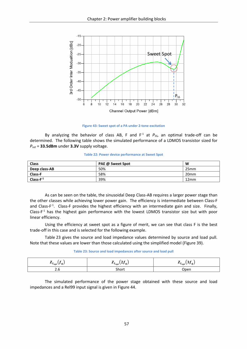
Chapter 2: Power amplifier building blocks
57
Figure 43: Sweet spot of a PA under 2-tone excitation
By analyzing the behavior of class AB, F and F-1 at PSS, an optimal trade-off can be determined. The following table shows the simulated performance of a LDMOS transistor sized for Psat = 33.5dBm under 3.3V supply voltage.
Table 22: Power device performance at Sweet Spot
Class PAE @ Sweet Spot W
Deep class-AB 50% 25mm
Class-F 58% 20mm
Class-F-1 39% 12mm
As can be seen on the table, the sinusoidal Deep Class-AB requires a larger power stage than the other classes while achieving lower power gain. The efficiency is intermediate between Class-F and Class-F-1. Class-F provides the highest efficiency with an intermediate gain and size. Finally, Class-F-1 has the highest gain performance with the lowest LDMOS transistor size but with poor linear efficiency.
Using the efficiency at sweet spot as a figure of merit, we can see that class F is the best trade-off in this case and is selected for the following example.
Table 23 gives the source and load impedance values determined by source and load pull. Note that these values are lower than those calculated using the simplified model (Figure 39).
Table 23: Source and load impedances after source and load pull
𝒁𝑳𝒐𝒑𝒕(𝒇𝟎) 𝒁𝑳𝒐𝒑𝒕(𝟐𝒇𝟎) 𝒁𝑳𝒐𝒑𝒕(𝟑𝒇𝟎)
2.6 Short Open
The simulated performance of the power stage obtained with these source and load impedances and a Rel99 input signal is given in Figure 44.
Sweet Spot
PSS
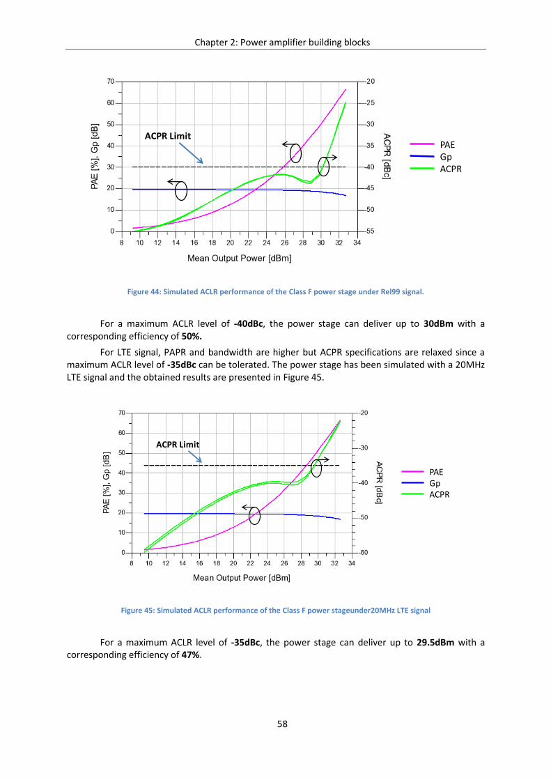
Chapter 2: Power amplifier building blocks
58
Figure 44: Simulated ACLR performance of the Class F power stage under Rel99 signal.
For a maximum ACLR level of -40dBc, the power stage can deliver up to 30dBm with a corresponding efficiency of 50%.
For LTE signal, PAPR and bandwidth are higher but ACPR specifications are relaxed since a maximum ACLR level of -35dBc can be tolerated. The power stage has been simulated with a 20MHz LTE signal and the obtained results are presented in Figure 45.
Figure 45: Simulated ACLR performance of the Class F power stageunder20MHz LTE signal
For a maximum ACLR level of -35dBc, the power stage can deliver up to 29.5dBm with a corresponding efficiency of 47%.
PAEGpACPR
ACPR Limit
PAEGpACPR
ACPR Limit
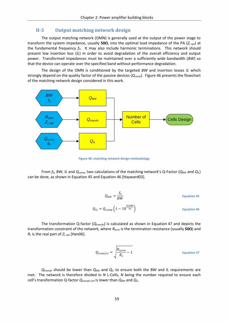
Chapter 2: Power amplifier building blocks
59
II-3 Output matching network design
The output matching network (OMN) is generally used at the output of the power stage to transform the system impedance, usually 50Ω, into the optimal load impedance of the PA (ZL opt) at the fundamental frequency f0. It may also include harmonic terminations. This network should present low insertion loss (IL) in order to avoid degradation of the overall efficiency and output power. Transformed impedances must be maintained over a sufficiently wide bandwidth (BW) so that the device can operate over the specified band without performance degradation.
The design of the OMN is conditioned by the targeted BW and insertion losses IL which strongly depend on the quality factor of the passive devices (Qcomp). Figure 46 presents the flowchart of the matching network design considered in this work.
Figure 46: matching network design methodology
From f0, BW, IL and Qcomp, two calculations of the matching network’s Q-Factor (QBW and QIL) can be done, as shown in Equation 45 and Equation 46 [Hayward03].
𝑄𝐵𝑊 =𝑓0𝐵𝑊
Equation 45
𝑄𝐼𝐿 = 𝑄𝑐𝑜𝑚𝑝 (1 − 10𝐼𝐿[𝑑𝐵]
20 ) Equation 46
The transformation Q-factor (Qtransfo) is calculated as shown in Equation 47 and depicts the transformation constraint of the network, where Rterm is the termination resistance (usually 50Ω) and RL is the real part of ZL opt [Han06].
𝑄𝑡𝑟𝑎𝑛𝑠𝑓𝑜 = √𝑅𝑡𝑒𝑟𝑚𝑅𝐿
− 1 Equation 47
Qtransfo should be lower than QBW and QIL to ensure both the BW and IL requirements are met. The network is therefore divided in N L-Cells, N being the number required to ensure each cell’s transformation Q-factor Qtransfo Cell is lower than QBW and QIL.
BW
f0
Cells DesignNumber of
CellsQtransfo
Qcomp
IL
QBW
QIL
Rterm
ZL opt
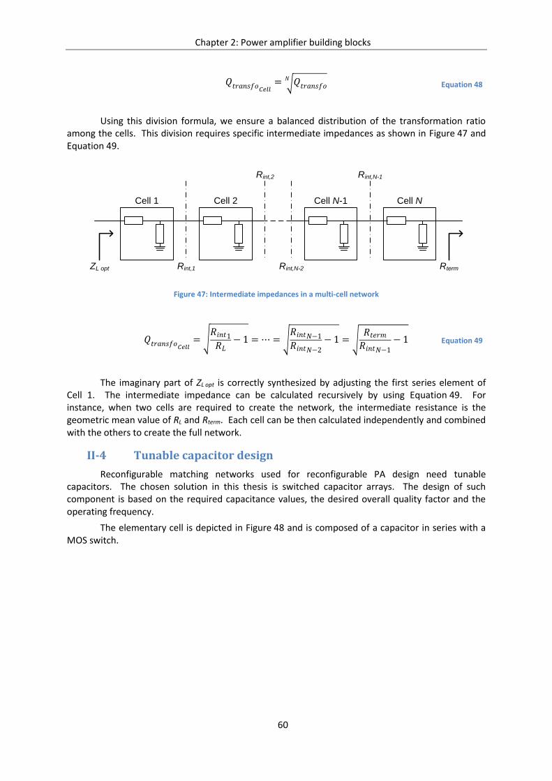
Chapter 2: Power amplifier building blocks
60
𝑄𝑡𝑟𝑎𝑛𝑠𝑓𝑜𝐶𝑒𝑙𝑙= √𝑄𝑡𝑟𝑎𝑛𝑠𝑓𝑜
𝑁 Equation 48
Using this division formula, we ensure a balanced distribution of the transformation ratio among the cells. This division requires specific intermediate impedances as shown in Figure 47 and Equation 49.
Figure 47: Intermediate impedances in a multi-cell network
𝑄𝑡𝑟𝑎𝑛𝑠𝑓𝑜𝐶𝑒𝑙𝑙= √
𝑅𝑖𝑛𝑡1𝑅𝐿
− 1 = ⋯ = √𝑅𝑖𝑛𝑡𝑁−1𝑅𝑖𝑛𝑡𝑁−2
− 1 = √𝑅𝑡𝑒𝑟𝑚𝑅𝑖𝑛𝑡𝑁−1
− 1 Equation 49
The imaginary part of ZL opt is correctly synthesized by adjusting the first series element of Cell 1. The intermediate impedance can be calculated recursively by using Equation 49. For instance, when two cells are required to create the network, the intermediate resistance is the geometric mean value of RL and Rterm. Each cell can be then calculated independently and combined with the others to create the full network.
II-4 Tunable capacitor design
Reconfigurable matching networks used for reconfigurable PA design need tunable capacitors. The chosen solution in this thesis is switched capacitor arrays. The design of such component is based on the required capacitance values, the desired overall quality factor and the operating frequency.
The elementary cell is depicted in Figure 48 and is composed of a capacitor in series with a MOS switch.
ZL opt RtermRint,1
Rint,N-1
Rint,N-2
Rint,2
Cell 1 Cell 2 Cell N-1 Cell N
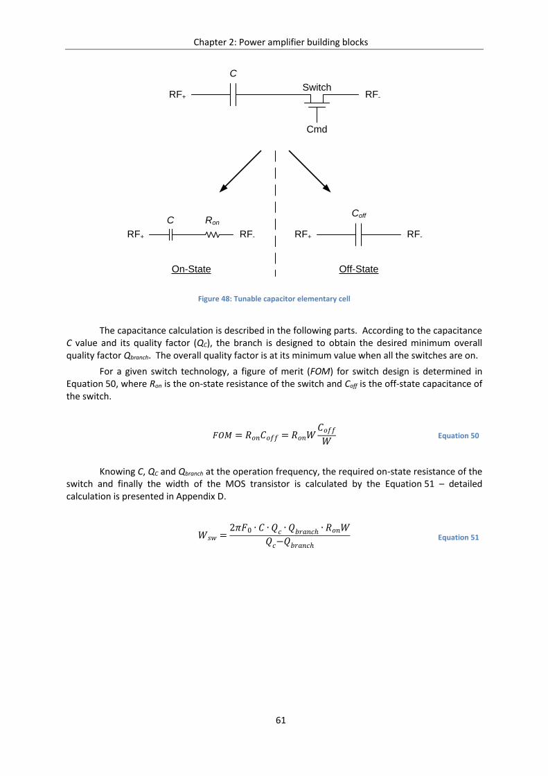
Chapter 2: Power amplifier building blocks
61
Figure 48: Tunable capacitor elementary cell
The capacitance calculation is described in the following parts. According to the capacitance C value and its quality factor (QC), the branch is designed to obtain the desired minimum overall quality factor Qbranch. The overall quality factor is at its minimum value when all the switches are on.
For a given switch technology, a figure of merit (FOM) for switch design is determined in Equation 50, where Ron is the on-state resistance of the switch and Coff is the off-state capacitance of the switch.
𝐹𝑂𝑀 = 𝑅𝑜𝑛𝐶𝑜𝑓𝑓 = 𝑅𝑜𝑛𝑊𝐶𝑜𝑓𝑓𝑊
Equation 50
Knowing C, QC and Qbranch at the operation frequency, the required on-state resistance of the switch and finally the width of the MOS transistor is calculated by the Equation 51 – detailed calculation is presented in Appendix D.
𝑊𝑠𝑤 =2𝜋𝐹0 ∙ 𝐶 ∙ 𝑄𝑐 ∙ 𝑄𝑏𝑟𝑎𝑛𝑐ℎ ∙ 𝑅𝑜𝑛𝑊
𝑄𝑐−𝑄𝑏𝑟𝑎𝑛𝑐ℎ Equation 51
C
SwitchRF+ RF-
Cmd
C
RF+ RF-
Ron
RF+ RF-
Coff
On-State Off-State

Chapter 2: Power amplifier building blocks
62
II-4.1. Switched capacitor bank
The schematic of a switched capacitor bank is given in Figure 49.
Figure 49: Schematic of a switched capacitor bank.
Equations 52 to 55 give the relation between the capacitance of each branch and their state – on or off – to obtain the equivalent capacitance.
𝐶0 + 𝐶1𝑜𝑓𝑓 + 𝐶2𝑜𝑓𝑓 +⋯+ 𝐶𝑛𝑜𝑓𝑓 = 𝐶𝑣𝑎𝑙1 Equation 52
𝐶0 + 𝐶1𝑜𝑛 + 𝐶2𝑜𝑓𝑓 +⋯+ 𝐶𝑛𝑜𝑓𝑓 = 𝐶𝑣𝑎𝑙2 Equation 53
𝐶0 + 𝐶1𝑜𝑛 + 𝐶2𝑜𝑛 +⋯+ 𝐶𝑛𝑜𝑓𝑓 = 𝐶𝑣𝑎𝑙3 Equation 54
⋮
𝐶0 + 𝐶1𝑜𝑛 + 𝐶2𝑜𝑛 +⋯+ 𝐶𝑛𝑜𝑛 = 𝐶𝑣𝑎𝑙𝑚 Equation 55
Those equations can be used to evaluate the capacitance step of each branch by calculating Ci on - Ci off. The following equations show the application to 3 capacitance values.
𝐶1𝑜𝑛 + 𝐶1𝑜𝑓𝑓 = 𝐶𝑣𝑎𝑙2 − 𝐶𝑣𝑎𝑙1 Equation 56
𝐶2𝑜𝑛 + 𝐶2𝑜𝑓𝑓 = 𝐶𝑣𝑎𝑙3 − 𝐶𝑣𝑎𝑙2 Equation 57
We consider that the off-state capacitance Ci off is a fraction of the on-state capacitance Ci on, see Equation 58.
C1
Switch 1
W1Cmd1
C2
Switch 2
W2
RF+
RF-
Cmd2
CN
Switch N
WNCmdN
C0

Chapter 2: Power amplifier building blocks
63
𝐶𝑖𝑜𝑓𝑓 = 𝑘𝑜𝑛 𝑜𝑓𝑓⁄ 𝐶𝑖𝑜𝑛 Equation 58
By setting kon/off as a tradeoff between expected interconnection parasitic and off-state capacitance of the MOS transistor, the capacitance of each branch can be determined as the following equations.
𝐶1 =𝐶𝑣𝑎𝑙2 − 𝐶𝑣𝑎𝑙1𝑘𝑜𝑛 𝑜𝑓𝑓⁄
Equation 59
𝐶2 =𝐶𝑣𝑎𝑙3 − 𝐶𝑣𝑎𝑙2𝑘𝑜𝑛 𝑜𝑓𝑓⁄
Equation 60
C0 is then determined by subtracting C1 and C2 from the maximal capacitance, see Equation 61.
𝐶0 = 𝐶𝑣𝑎𝑙3 − 𝐶1 − 𝐶2 Equation 61
Once all the branches’ capacitance values have been determined, each independent branch can be fully sized from the desired Qbranch using the methodology presented in the previous part. Another application that is worth studying is the binary weighted switched capacitor array.
The switched capacitor array should be able to withstand high power. When submitted to high power, the different branches may withstand high RF voltage (VRF). While the switch is on, only the capacitor (C) withstands the full excursion of the RF voltage. The required number of capacitors in series (NC) is obtained by considering the breakdown voltage (Vbk C) of each unity capacitor (Cu). Then, the capacitance values of each capacitor Cu must be multiplied by the number of capacitors to obtain the same overall capacitance C.
Figure 50:Voltage distribution across a capacitor branch in on-state
𝑁𝐶 =𝑉𝑅𝐹𝑉𝑏𝑘𝐶
Equation 62
𝐶𝑢 = 𝐶 ∙ 𝑁𝐶 Equation 63
CU CU
NC capacitors
VSW,on ≈ 0
VC ≈ VRF
VC,uVC,u
RF+ RF-
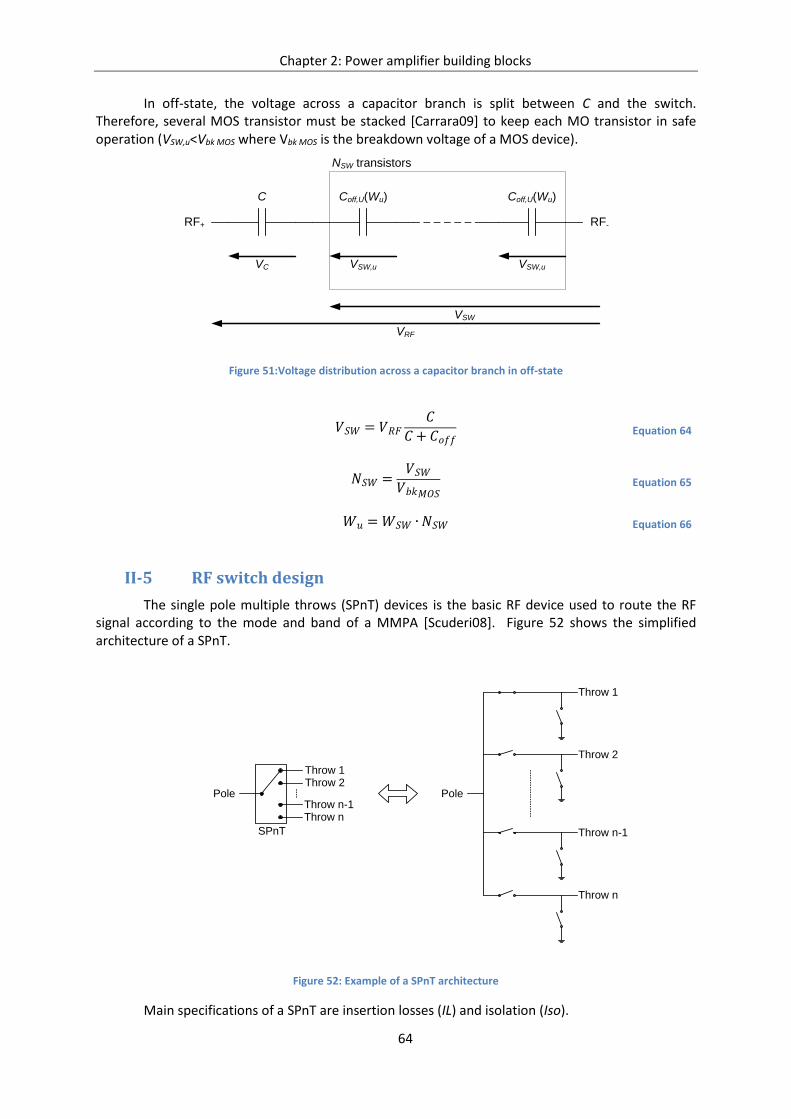
Chapter 2: Power amplifier building blocks
64
In off-state, the voltage across a capacitor branch is split between C and the switch. Therefore, several MOS transistor must be stacked [Carrara09] to keep each MO transistor in safe operation (VSW,u<Vbk MOS where Vbk MOS is the breakdown voltage of a MOS device).
Figure 51:Voltage distribution across a capacitor branch in off-state
𝑉𝑆𝑊 = 𝑉𝑅𝐹𝐶
𝐶+ 𝐶𝑜𝑓𝑓 Equation 64
𝑁𝑆𝑊 =𝑉𝑆𝑊𝑉𝑏𝑘𝑀𝑂𝑆
Equation 65
𝑊𝑢 =𝑊𝑆𝑊 ∙ 𝑁𝑆𝑊 Equation 66
II-5 RF switch design
The single pole multiple throws (SPnT) devices is the basic RF device used to route the RF signal according to the mode and band of a MMPA [Scuderi08]. Figure 52 shows the simplified architecture of a SPnT.
Figure 52: Example of a SPnT architecture
Main specifications of a SPnT are insertion losses (IL) and isolation (Iso).
Coff,U(Wu)
NSW transistors
VC
VSW
VSW,u VSW,u
RF+ RF-
C Coff,U(Wu)
VRF
Pole
Throw 1
Throw 2
Throw n-1
Throw n
SPnT
Pole
Throw 1Throw 2
Throw n-1Throw n
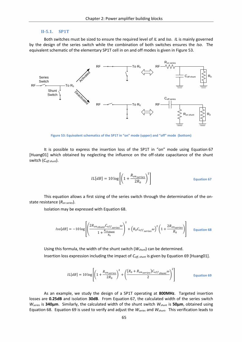
Chapter 2: Power amplifier building blocks
65
II-5.1. SP1T
Both switches must be sized to ensure the required level of IL and Iso. IL is mainly governed by the design of the series switch while the combination of both switches ensures the Iso. The equivalent schematic of the elementary SP1T cell in on and off modes is given in Figure 53.
Figure 53: Equivalent schematics of the SP1T in “on” mode (upper) and “off” mode (bottom)
It is possible to express the insertion loss of the SP1T in “on” mode using Equation 67 [Huang01] which obtained by neglecting the influence on the off-state capacitance of the shunt switch (Coff shunt).
𝐼𝐿[𝑑𝐵] = 10 log [(1 +𝑅𝑜𝑛𝑠𝑒𝑟𝑖𝑒𝑠2𝑅0
)
2
] Equation 67
This equation allows a first sizing of the series switch through the determination of the on-state resistance (Ron series).
Isolation may be expressed with Equation 68.
𝐼𝑠𝑜[𝑑𝐵] = −10 log [(2𝑅𝑜𝑛𝑠ℎ𝑢𝑛𝑡𝐶𝑜𝑓𝑓𝑠𝑒𝑟𝑖𝑒𝑠
𝜔
1 +𝑅𝑜𝑛𝑠ℎ𝑢𝑛𝑡
𝑅0
)
2
+ (𝑅0𝐶𝑜𝑓𝑓𝑠𝑒𝑟𝑖𝑒𝑠𝜔)
2(1 +
2𝑅𝑜𝑛𝑠𝑒𝑟𝑖𝑒𝑠𝑅0
)] Equation 68
Using this formula, the width of the shunt switch (Wshunt) can be determined.
Insertion loss expression including the impact of Coff, shunt is given by Equation 69 [Huang01].
𝐼𝐿[𝑑𝐵] = 10 log [(1 +𝑅𝑜𝑛𝑠𝑒𝑟𝑖𝑒𝑠2𝑅0
)
2
+ ((𝑅0 + 𝑅𝑜𝑛𝑠𝑒𝑟𝑖𝑒𝑠)𝐶𝑜𝑓𝑓𝑠ℎ𝑢𝑛𝑡
𝜔
2)
2
] Equation 69
As an example, we study the design of a SP1T operating at 800MHz. Targeted insertion losses are 0.25dB and isolation 30dB. From Equation 67, the calculated width of the series switch Wseries is 340µm. Similarly, the calculated width of the shunt switch Wshunt is 50µm, obtained using Equation 68. Equation 69 is used to verify and adjust the Wseries and Wshunt. This verification leads to
Activat
ed
Deactivated
R0
Ron series
Coff shunt
RF
Ron shunt R0
Coff series
RF
Series
Switch
Shunt
Switch
RF To R0
RF To R0
RF To R0
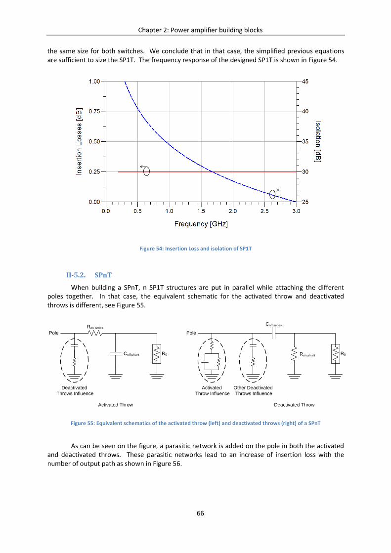
Chapter 2: Power amplifier building blocks
66
the same size for both switches. We conclude that in that case, the simplified previous equations are sufficient to size the SP1T. The frequency response of the designed SP1T is shown in Figure 54.
Figure 54: Insertion Loss and isolation of SP1T
II-5.2. SPnT
When building a SPnT, n SP1T structures are put in parallel while attaching the different poles together. In that case, the equivalent schematic for the activated throw and deactivated throws is different, see Figure 55.
Figure 55: Equivalent schematics of the activated throw (left) and deactivated throws (right) of a SPnT
As can be seen on the figure, a parasitic network is added on the pole in both the activated and deactivated throws. These parasitic networks lead to an increase of insertion loss with the number of output path as shown in Figure 56.
Activated Throw
R0
Ron,series
Coff,shunt
Pole
Deactivated
Throws Influence
Deactivated Throw
Ron,shunt R0
Coff,series
Pole
Other Deactivated
Throws Influence
Activated
Throw Influence
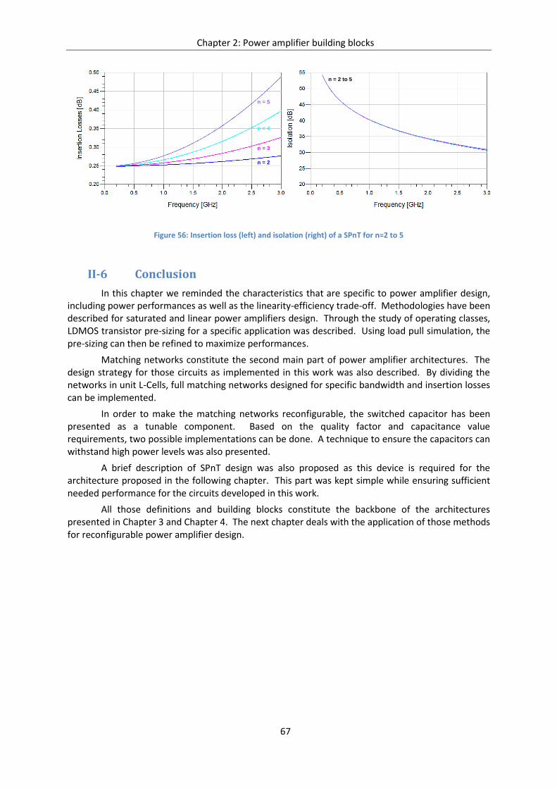
Chapter 2: Power amplifier building blocks
67
Figure 56: Insertion loss (left) and isolation (right) of a SPnT for n=2 to 5
II-6 Conclusion
In this chapter we reminded the characteristics that are specific to power amplifier design, including power performances as well as the linearity-efficiency trade-off. Methodologies have been described for saturated and linear power amplifiers design. Through the study of operating classes, LDMOS transistor pre-sizing for a specific application was described. Using load pull simulation, the pre-sizing can then be refined to maximize performances.
Matching networks constitute the second main part of power amplifier architectures. The design strategy for those circuits as implemented in this work was also described. By dividing the networks in unit L-Cells, full matching networks designed for specific bandwidth and insertion losses can be implemented.
In order to make the matching networks reconfigurable, the switched capacitor has been presented as a tunable component. Based on the quality factor and capacitance value requirements, two possible implementations can be done. A technique to ensure the capacitors can withstand high power levels was also presented.
A brief description of SPnT design was also proposed as this device is required for the architecture proposed in the following chapter. This part was kept simple while ensuring sufficient needed performance for the circuits developed in this work.
All those definitions and building blocks constitute the backbone of the architectures presented in Chapter 3 and Chapter 4. The next chapter deals with the application of those methods for reconfigurable power amplifier design.
n = 2 to 5
n = 2
n = 3
n = 4
n = 5

Chapter 2: Power amplifier building blocks
68
II-7 References
[Carvalho02] N. B. de Carvalho and J. C. Pedro, “A Comprehensive Explanation of Distortion Sideband Asymmetries”, IEEE Transactions on Microwave Theory and Techniques, vol. 50, pp. 2090-2101, September 2002.
[Cripps06] S.-C. Cripps, “RF Power Amplifier for Wireless Applications – 2nd edition”, Artech House, 2006.
[Hallman32] L. B. Hallman, “A Fourier Analysis of Radio-Frequency Power Amplifier wave Forms”, Proceedings of Institute of Radio Engineers, vol. 23, pp. 1640-1659, October 1932.
[Han06] Y. Han and D. J. Perreault, “Analysis and design of High Efficiency Matching Networks”, IEEE Transactions on Power Electronics, vol. 21, pp. 1484-1491, September 2006.
[Hayward03] W. Hayward, R. Campbell and B. Larkin, “Experimental Methods and RF Design”, ARRL Press, 2003.
[Huang01] F.-J. Huang and K. O, “A 0.5-µm CMOS T/R switch for 900-MHz Wireless Applications”, IEEE Journal of Solid-State Circuits, vol. 36, pp. 486-492, March 2001.
[Kim10] D. Kim, J. Choi, D. Kang, B. Kim, “High Efficiency and Wideband Envelope Tracking Power Amplifier with Sweet Spot Tracking”, IEEE Radio Frequency Integrated Circuit Symposium, pp. 255-258, May 2010.
[Kim11] J. H. Kim, G. D. Jo, J. H. Kim, K. C. Lee and J. H. Jung, “Modeling and Design Methodology of High Efficiency Class-F and Class-F-1 Power Amplifiers”, IEEE Transactions on Microwave Theory and Techniques, vol. 59, pp. 153-165, January 2011.
[Scuderi08] A. Scuderi, C. D. Presti, F. Carrara, B. Rauber and G. Palminsano, “A Stage-Bypass SOI-CMOS Switch for Multi-Mode Multi-Band Applications”, IEEE Radio Frequency Integrated Circuit Symposium, pp. 325-328, June 2008.
[Stancliff79] R. B. Stancliff and D. D. Poulin, “Harmonic Load-Pull”, IEEE International Microwave Symposium, pp. 185-187, May 1979.

69
Chapter III: Reconfigurable Multi-Mode Multi-Band Power Amplifier Design
III-1 Introduction
Reconfigurable PA architectures are the best solutions to increase the integration level and reduce the cost of multimode multiband power amplifiers (MMPA). In this chapter, a new reconfigurable MMPA architecture is proposed and implemented in SOI CMOS technology.
The architecture of the reconfigurable MMPA is first presented, as well as the strategy used to handle multiple modes and frequency bands. The power output stage is the major contributor to the large signal PA performances together with the output matching network. The power stage uses LDMOS transistor sizing to handle the power requirements in saturated and linear modes. The tunable output matching network is optimized to realize optimal matching in the targeted frequency bands.
Assembling the driver and output stage has an impact on the overall PA performance. Anticipating the degradation in terms of efficiency helps setting the requirements for the driver stage, inter-stage matching network and input matching network. A trade-off is chosen to limit the overall performance degradation associated to the driver stage. Afterwards, the input matching network is designed to ensure a maximal power transfer to the driver’s input in every mode.
The design of the inter-stage matching consists in choosing the adequate topology that can realize optimal inter-stage matching. The focus during this design step is to ensure that optimal source impedance is presented to the power stage, thus avoiding performance degradation. A trade-off for the value of load impedance of the driver stage is then found to ensure correct overall performance.
In order to operate properly in linear mode, the architecture requires an adequate biasing strategy. A bias circuit limiting memory effects is proposed. Source harmonic termination is combined with the bias circuit to reach a more compact design.
Finally, the performance of the proposed reconfigurable PA architecture is assessed through measurement and compared with the state of the art.
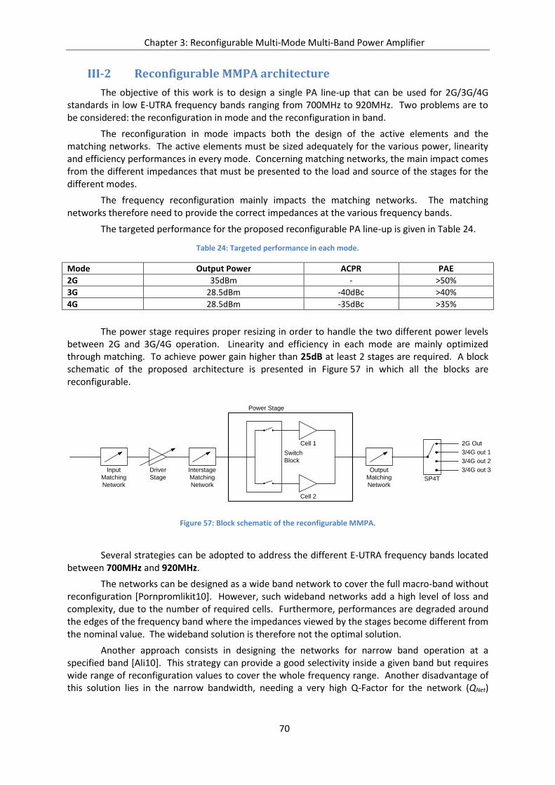
Chapter 3: Reconfigurable Multi-Mode Multi-Band Power Amplifier
70
III-2 Reconfigurable MMPA architecture
The objective of this work is to design a single PA line-up that can be used for 2G/3G/4G standards in low E-UTRA frequency bands ranging from 700MHz to 920MHz. Two problems are to be considered: the reconfiguration in mode and the reconfiguration in band.
The reconfiguration in mode impacts both the design of the active elements and the matching networks. The active elements must be sized adequately for the various power, linearity and efficiency performances in every mode. Concerning matching networks, the main impact comes from the different impedances that must be presented to the load and source of the stages for the different modes.
The frequency reconfiguration mainly impacts the matching networks. The matching networks therefore need to provide the correct impedances at the various frequency bands.
The targeted performance for the proposed reconfigurable PA line-up is given in Table 24.
Table 24: Targeted performance in each mode.
Mode Output Power ACPR PAE
2G 35dBm - >50%
3G 28.5dBm -40dBc >40%
4G 28.5dBm -35dBc >35%
The power stage requires proper resizing in order to handle the two different power levels between 2G and 3G/4G operation. Linearity and efficiency in each mode are mainly optimized through matching. To achieve power gain higher than 25dB at least 2 stages are required. A block schematic of the proposed architecture is presented in Figure 57 in which all the blocks are reconfigurable.
Figure 57: Block schematic of the reconfigurable MMPA.
Several strategies can be adopted to address the different E-UTRA frequency bands located between 700MHz and 920MHz.
The networks can be designed as a wide band network to cover the full macro-band without reconfiguration [Pornpromlikit10]. However, such wideband networks add a high level of loss and complexity, due to the number of required cells. Furthermore, performances are degraded around the edges of the frequency band where the impedances viewed by the stages become different from the nominal value. The wideband solution is therefore not the optimal solution.
Another approach consists in designing the networks for narrow band operation at a specified band [Ali10]. This strategy can provide a good selectivity inside a given band but requires wide range of reconfiguration values to cover the whole frequency range. Another disadvantage of this solution lies in the narrow bandwidth, needing a very high Q-Factor for the network (QNet)
Driver
Stage
Cell 1
Cell 2
SP4T
2G Out
3/4G out 1
3/4G out 2
3/4G out 3
Power Stage
Input
Matching
Network
Interstage
Matching
Network
Output
Matching
Network
Switch
Block
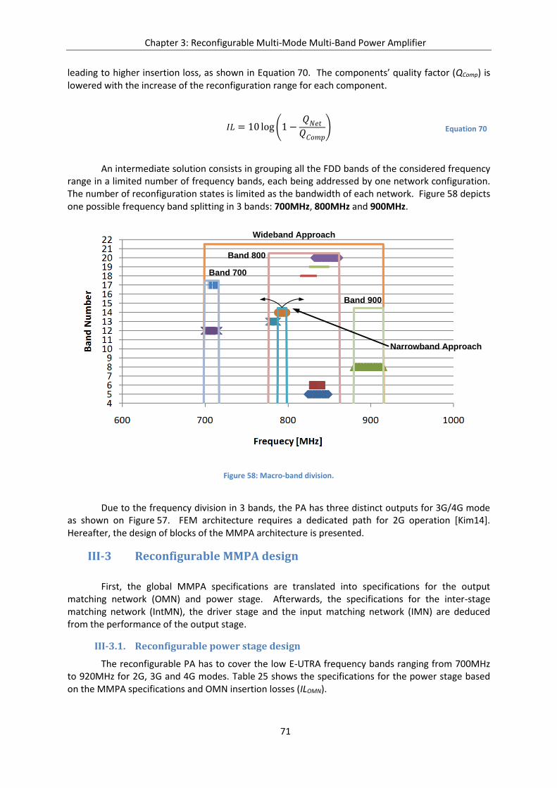
Chapter 3: Reconfigurable Multi-Mode Multi-Band Power Amplifier
71
leading to higher insertion loss, as shown in Equation 70. The components’ quality factor (QComp) is lowered with the increase of the reconfiguration range for each component.
𝐼𝐿 = 10 log(1 −𝑄𝑁𝑒𝑡𝑄𝐶𝑜𝑚𝑝
) Equation 70
An intermediate solution consists in grouping all the FDD bands of the considered frequency range in a limited number of frequency bands, each being addressed by one network configuration. The number of reconfiguration states is limited as the bandwidth of each network. Figure 58 depicts one possible frequency band splitting in 3 bands: 700MHz, 800MHz and 900MHz.
Figure 58: Macro-band division.
Due to the frequency division in 3 bands, the PA has three distinct outputs for 3G/4G mode as shown on Figure 57. FEM architecture requires a dedicated path for 2G operation [Kim14]. Hereafter, the design of blocks of the MMPA architecture is presented.
III-3 Reconfigurable MMPA design
First, the global MMPA specifications are translated into specifications for the output matching network (OMN) and power stage. Afterwards, the specifications for the inter-stage matching network (IntMN), the driver stage and the input matching network (IMN) are deduced from the performance of the output stage.
III-3.1. Reconfigurable power stage design
The reconfigurable PA has to cover the low E-UTRA frequency bands ranging from 700MHz to 920MHz for 2G, 3G and 4G modes. Table 25 shows the specifications for the power stage based on the MMPA specifications and OMN insertion losses (ILOMN).
Wideband Approach
Band 700
Band 900
Band 800
Narrowband Approach
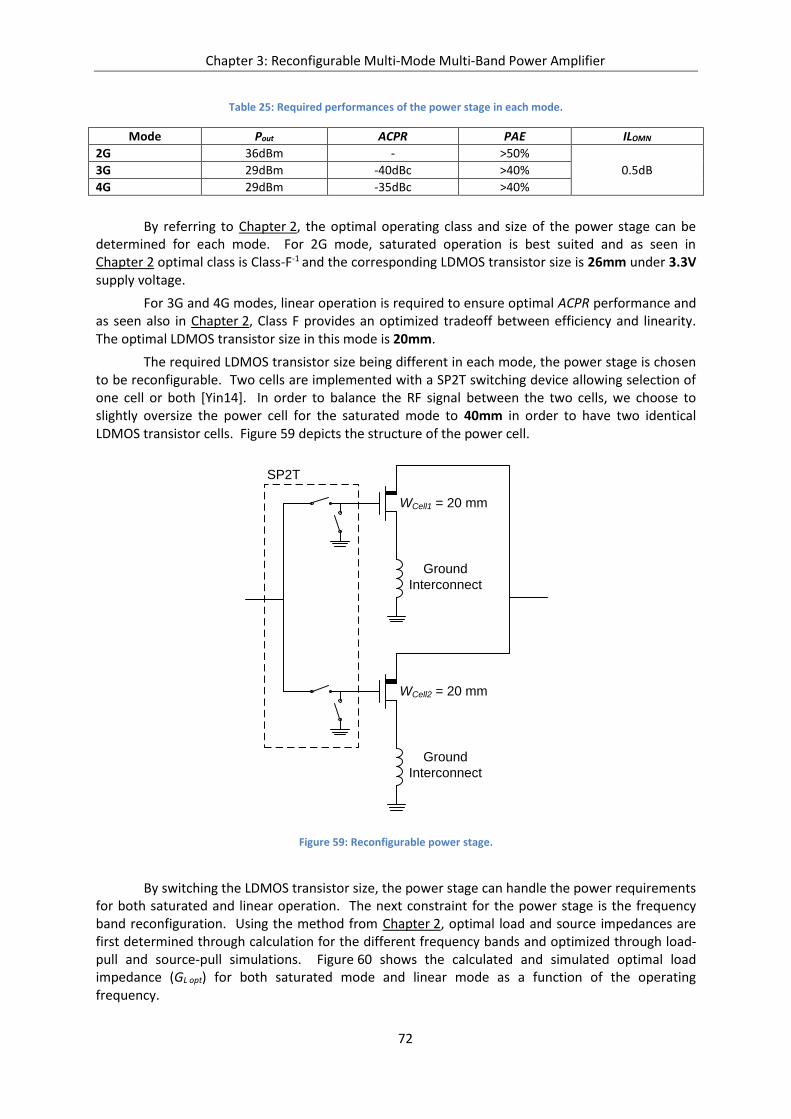
Chapter 3: Reconfigurable Multi-Mode Multi-Band Power Amplifier
72
Table 25: Required performances of the power stage in each mode.
Mode Pout ACPR PAE ILOMN
2G 36dBm - >50%
0.5dB 3G 29dBm -40dBc >40%
4G 29dBm -35dBc >40%
By referring to Chapter 2, the optimal operating class and size of the power stage can be determined for each mode. For 2G mode, saturated operation is best suited and as seen in Chapter 2 optimal class is Class-F-1 and the corresponding LDMOS transistor size is 26mm under 3.3V supply voltage.
For 3G and 4G modes, linear operation is required to ensure optimal ACPR performance and as seen also in Chapter 2, Class F provides an optimized tradeoff between efficiency and linearity. The optimal LDMOS transistor size in this mode is 20mm.
The required LDMOS transistor size being different in each mode, the power stage is chosen to be reconfigurable. Two cells are implemented with a SP2T switching device allowing selection of one cell or both [Yin14]. In order to balance the RF signal between the two cells, we choose to slightly oversize the power cell for the saturated mode to 40mm in order to have two identical LDMOS transistor cells. Figure 59 depicts the structure of the power cell.
Figure 59: Reconfigurable power stage.
By switching the LDMOS transistor size, the power stage can handle the power requirements for both saturated and linear operation. The next constraint for the power stage is the frequency band reconfiguration. Using the method from Chapter 2, optimal load and source impedances are first determined through calculation for the different frequency bands and optimized through load-pull and source-pull simulations. Figure 60 shows the calculated and simulated optimal load impedance (GL opt) for both saturated mode and linear mode as a function of the operating frequency.
WCell1 = 20 mm
WCell2 = 20 mm
Ground
Interconnect
SP2T
Ground
Interconnect
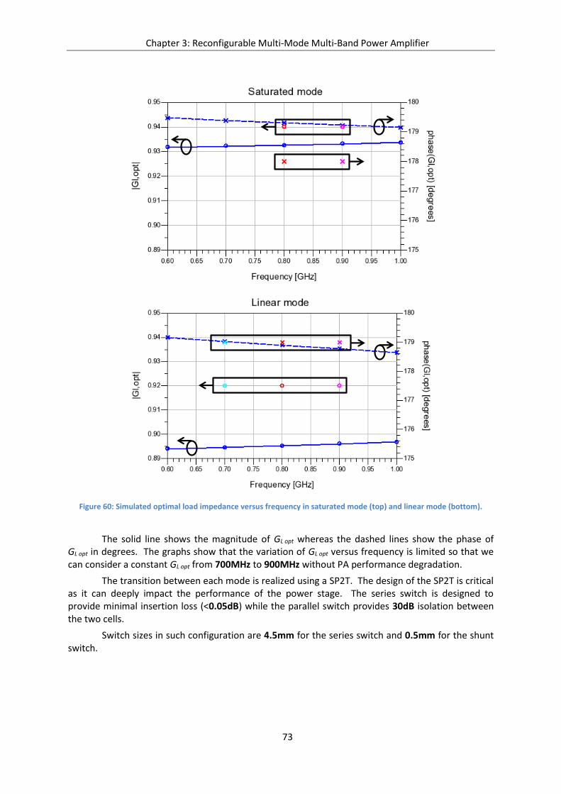
Chapter 3: Reconfigurable Multi-Mode Multi-Band Power Amplifier
73
Figure 60: Simulated optimal load impedance versus frequency in saturated mode (top) and linear mode (bottom).
The solid line shows the magnitude of GL opt whereas the dashed lines show the phase of GL opt in degrees. The graphs show that the variation of GL opt versus frequency is limited so that we can consider a constant GL opt from 700MHz to 900MHz without PA performance degradation.
The transition between each mode is realized using a SP2T. The design of the SP2T is critical as it can deeply impact the performance of the power stage. The series switch is designed to provide minimal insertion loss (<0.05dB) while the parallel switch provides 30dB isolation between the two cells.
Switch sizes in such configuration are 4.5mm for the series switch and 0.5mm for the shunt switch.
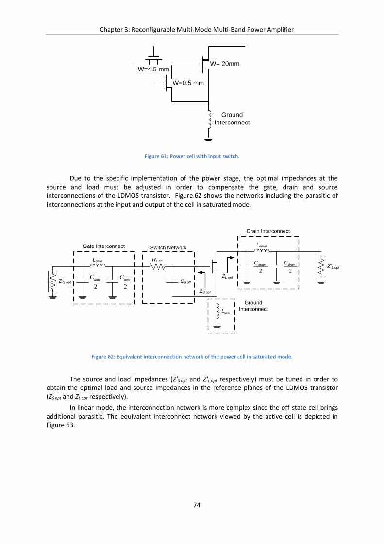
Chapter 3: Reconfigurable Multi-Mode Multi-Band Power Amplifier
74
Figure 61: Power cell with input switch.
Due to the specific implementation of the power stage, the optimal impedances at the source and load must be adjusted in order to compensate the gate, drain and source interconnections of the LDMOS transistor. Figure 62 shows the networks including the parasitic of interconnections at the input and output of the cell in saturated mode.
Figure 62: Equivalent interconnection network of the power cell in saturated mode.
The source and load impedances (Z’S opt and Z’L opt respectively) must be tuned in order to obtain the optimal load and source impedances in the reference planes of the LDMOS transistor (ZS opt and ZL opt respectively).
In linear mode, the interconnection network is more complex since the off-state cell brings additional parasitic. The equivalent interconnect network viewed by the active cell is depicted in Figure 63.
W= 20mmW=4.5 mm
W=0.5 mm
Ground
Interconnect
Ground
Interconnect
Cp off
Rs on
2
drainC
2
drainC
Drain Interconnect
Gate Interconnect Switch Network
Z’S opt
Lgate
2
gateC
2
gateC
Lgnd
Ldrain
Z’L opt
ZS opt
ZL opt
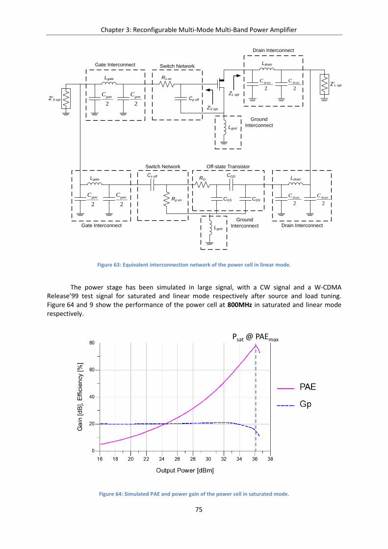
Chapter 3: Reconfigurable Multi-Mode Multi-Band Power Amplifier
75
Figure 63: Equivalent interconnection network of the power cell in linear mode.
The power stage has been simulated in large signal, with a CW signal and a W-CDMA Release’99 test signal for saturated and linear mode respectively after source and load tuning. Figure 64 and 9 show the performance of the power cell at 800MHz in saturated and linear mode respectively.
Figure 64: Simulated PAE and power gain of the power cell in saturated mode.
Ground
Interconnect
Cp off
Rs on
2
drainC
2
drainC
Drain Interconnect
Gate Interconnect Switch Network
Lgate
2
gateC
2
gateC
Lgnd
Ldrain
Z’L opt
ZS opt
ZL opt
Ground
Interconnect
Cs off
Rp on2
drainC
2
drainC
Drain InterconnectGate Interconnect
Switch Network
Lgate
2
gateC
2
gateC
Lgnd
Ldrain
CGS
RG
CDS
CGD
Z’S opt
Off-state Transistor
Psat @ PAEmax
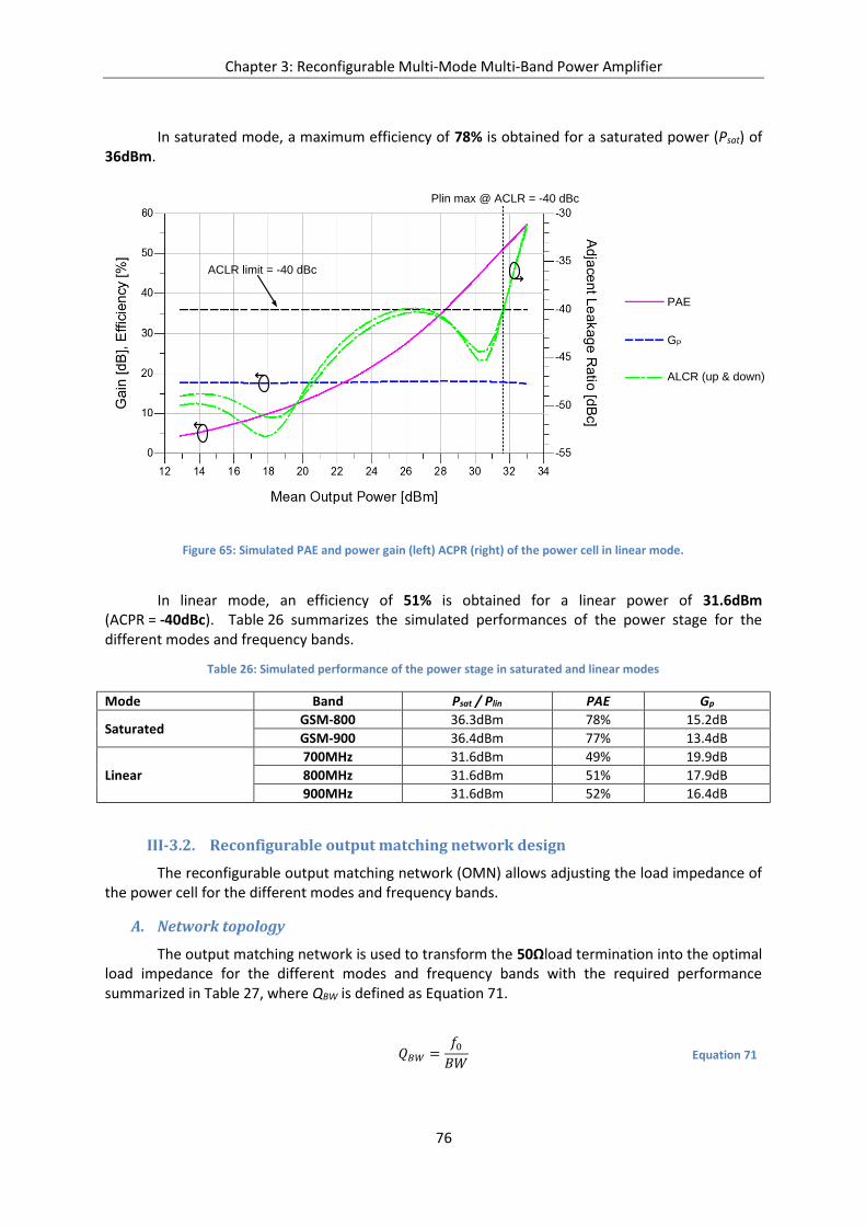
Chapter 3: Reconfigurable Multi-Mode Multi-Band Power Amplifier
76
In saturated mode, a maximum efficiency of 78% is obtained for a saturated power (Psat) of 36dBm.
Figure 65: Simulated PAE and power gain (left) ACPR (right) of the power cell in linear mode.
In linear mode, an efficiency of 51% is obtained for a linear power of 31.6dBm (ACPR = -40dBc). Table 26 summarizes the simulated performances of the power stage for the different modes and frequency bands.
Table 26: Simulated performance of the power stage in saturated and linear modes
Mode Band Psat / Plin PAE Gp
Saturated GSM-800 36.3dBm 78% 15.2dB
GSM-900 36.4dBm 77% 13.4dB
Linear
700MHz 31.6dBm 49% 19.9dB
800MHz 31.6dBm 51% 17.9dB
900MHz 31.6dBm 52% 16.4dB
III-3.2. Reconfigurable output matching network design
The reconfigurable output matching network (OMN) allows adjusting the load impedance of the power cell for the different modes and frequency bands.
A. Network topology
The output matching network is used to transform the 50Ωload termination into the optimal load impedance for the different modes and frequency bands with the required performance summarized in Table 27, where QBW is defined as Equation 71.
𝑄𝐵𝑊 =𝑓0𝐵𝑊
Equation 71
Plin max @ ACLR = -40 dBc
PAE
GP
ALCR (up & down)
ACLR limit = -40 dBc

Chapter 3: Reconfigurable Multi-Mode Multi-Band Power Amplifier
77
Table 27: required Q-Factor as a function of the frequency band.
Band Band 700 Band 800 Band 900
Bandwidth (BW) 17MHz 85MHz 35MHz
f0 707.5MHz 819.5MHz 897.5MHz
QBW 42 10 26
In order to realize matching, we first need to calculate the transformation Q-Factor (QTransfo OMN) defined as follows in Equation 72.
𝑄𝑇𝑟𝑎𝑛𝑠𝑓𝑜𝑂𝑀𝑁= √
50
𝑅𝐿𝑜𝑝𝑡− 1 Equation 72
In order to meet both the frequency and IL requirements, QTransfo OMN should be lower than the desired QBW and Insertion Loss Q-Factor (QIL). The number of cells in the network is chosen to verify this condition. The optimal load impedances are given in Table 28.
Table 28: Optimal load impedance in saturated and linear modes.
Mode Saturated Linear
RL opt 2.1Ω 2.9Ω
QTransfo OMN 4.78 4.03
In our case, the maximum QTransfo OMN (4.78) is lower than the lowest QBW (10). In this case, 1 cell is sufficient to meet the frequency requirements.
QIL is determined from the desired insertion loss (IL) and the minimum components Q-Factor (QComp) with Equation 68.
𝑄𝐼𝐿 = 𝑄𝐶𝑜𝑚𝑝 (1 − 10−𝐼𝐿[𝑑𝐵]
20 ) Equation 73
By considering QComp targeted ILare40 and is 0.5dB respectively, QIL is equal to 2.23. Since QTransfo OMN is higher than QIL, one cell is not sufficient to meet the requirements. By adding a second cell, QTransfo OMN is reduced to 2.2, thus meeting both frequency and loss requirements.
The chosen network structure is shown in Figure 66
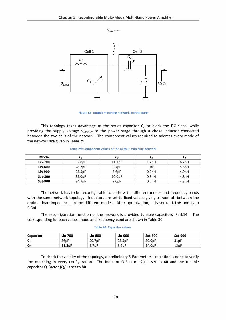
Chapter 3: Reconfigurable Multi-Mode Multi-Band Power Amplifier
78
Figure 66: output matching network architecture
This topology takes advantage of the series capacitor C2 to block the DC signal while providing the supply voltage VDD PWR to the power stage through a choke inductor connected between the two cells of the network. The component values required to address every mode of the network are given in Table 29.
Table 29: Component values of the output matching network
Mode C1 C2 L1 L2
Lin-700 32.8pF 11.1pF 1.2nH 6.2nH
Lin-800 28.7pF 9.7pF 1nH 5.5nH
Lin-900 25.5pF 8.6pF 0.9nH 4.9nH
Sat-800 39.0pF 10.0pF 0.8nH 4.8nH
Sat-900 34.7pF 9.0pF 0.7nH 4.3nH
The network has to be reconfigurable to address the different modes and frequency bands with the same network topology. Inductors are set to fixed values giving a trade-off between the optimal load impedances in the different modes. After optimization, L1 is set to 1.1nH and L2 to 5.5nH.
The reconfiguration function of the network is provided tunable capacitors [Park14]. The corresponding for each values mode and frequency band are shown in Table 30.
Table 30: Capacitor values.
Capacitor Lin-700 Lin-800 Lin-900 Sat-800 Sat-900
C1 36pF 29.7pF 25.5pF 39.0pF 31pF
C2 11.5pF 9.7pF 8.6pF 14.0pF 12pF
To check the validity of the topology, a preliminary S-Parameters simulation is done to verify the matching in every configuration. The inductor Q-Factor (QL) is set to 40 and the tunable capacitor Q-Factor (QC) is set to 80.
VDD PWR
L1
L2C1
C2
Cell 1 Cell 2
ZL opt 50 W
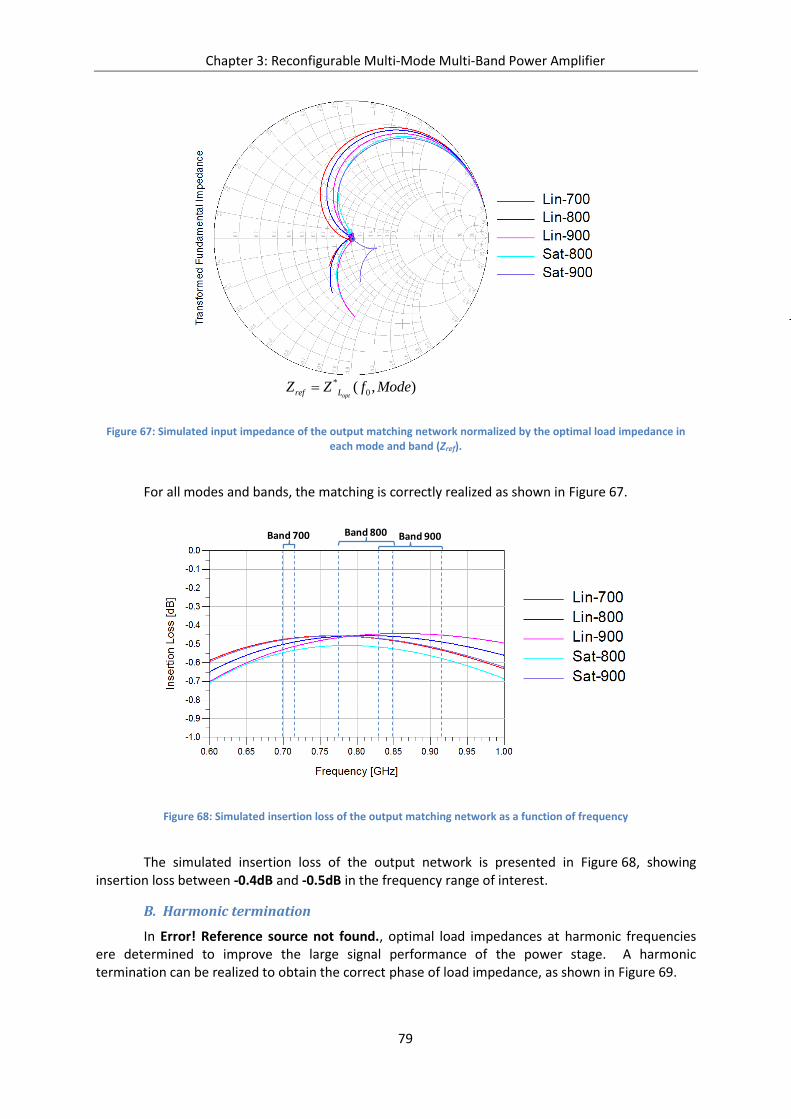
Chapter 3: Reconfigurable Multi-Mode Multi-Band Power Amplifier
79
Figure 67: Simulated input impedance of the output matching network normalized by the optimal load impedance in each mode and band (Zref).
For all modes and bands, the matching is correctly realized as shown in Figure 67.
Figure 68: Simulated insertion loss of the output matching network as a function of frequency
The simulated insertion loss of the output network is presented in Figure 68, showing insertion loss between -0.4dB and -0.5dB in the frequency range of interest.
B. Harmonic termination
In Error! Reference source not found., optimal load impedances at harmonic frequencies ere determined to improve the large signal performance of the power stage. A harmonic termination can be realized to obtain the correct phase of load impedance, as shown in Figure 69.
*
0( , )optref LZ Z f Mode
Band 900Band 800Band 700
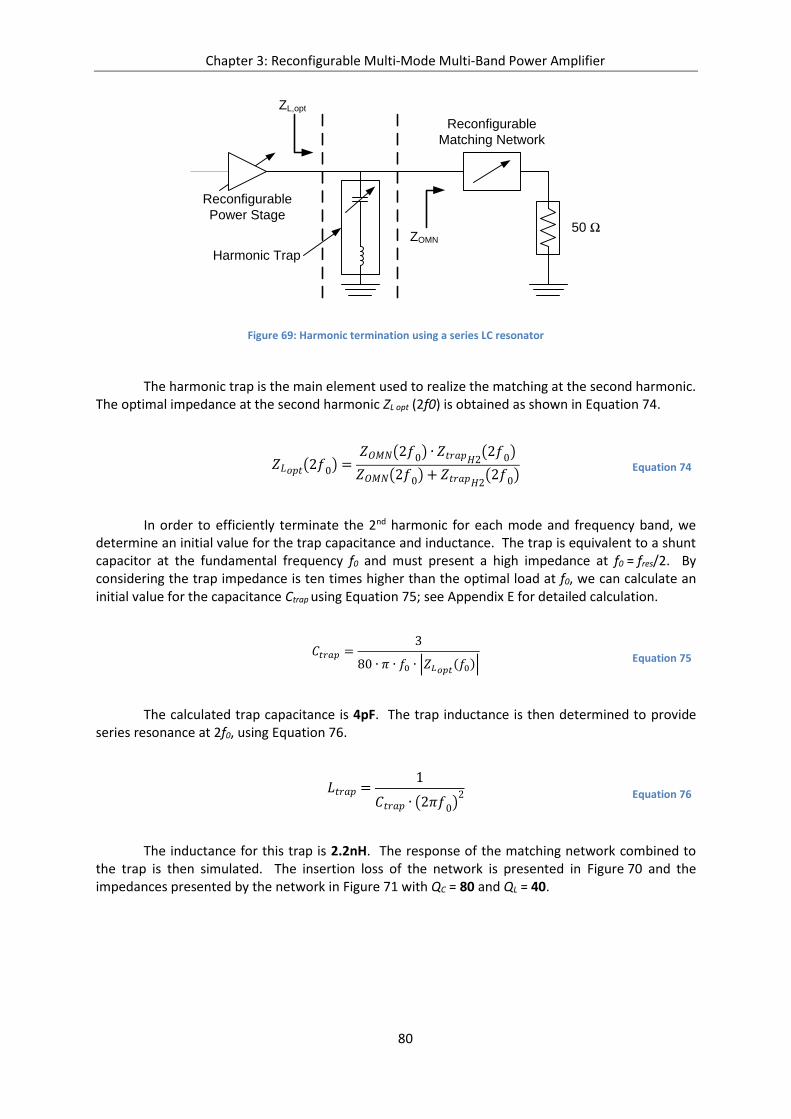
Chapter 3: Reconfigurable Multi-Mode Multi-Band Power Amplifier
80
Figure 69: Harmonic termination using a series LC resonator
The harmonic trap is the main element used to realize the matching at the second harmonic. The optimal impedance at the second harmonic ZL opt (2f0) is obtained as shown in Equation 74.
𝑍𝐿𝑜𝑝𝑡(2𝑓0) =𝑍𝑂𝑀𝑁(2𝑓0) ∙ 𝑍𝑡𝑟𝑎𝑝𝐻2(2𝑓0)
𝑍𝑂𝑀𝑁(2𝑓0)+𝑍𝑡𝑟𝑎𝑝𝐻2(2𝑓0) Equation 74
In order to efficiently terminate the 2nd harmonic for each mode and frequency band, we determine an initial value for the trap capacitance and inductance. The trap is equivalent to a shunt capacitor at the fundamental frequency f0 and must present a high impedance at f0 = fres/2. By considering the trap impedance is ten times higher than the optimal load at f0, we can calculate an initial value for the capacitance Ctrap using Equation 75; see Appendix E for detailed calculation.
𝐶𝑡𝑟𝑎𝑝 =3
80 ∙ 𝜋 ∙ 𝑓0 ∙ |𝑍𝐿𝑜𝑝𝑡(𝑓0)|
Equation 75
The calculated trap capacitance is 4pF. The trap inductance is then determined to provide series resonance at 2f0, using Equation 76.
𝐿𝑡𝑟𝑎𝑝 =1
𝐶𝑡𝑟𝑎𝑝 ∙ (2𝜋𝑓0)2
Equation 76
The inductance for this trap is 2.2nH. The response of the matching network combined to the trap is then simulated. The insertion loss of the network is presented in Figure 70 and the impedances presented by the network in Figure 71 with QC = 80 and QL = 40.
Reconfigurable
Power Stage
Reconfigurable
Matching Network
50 ΩZOMN
ZL,opt
Harmonic Trap
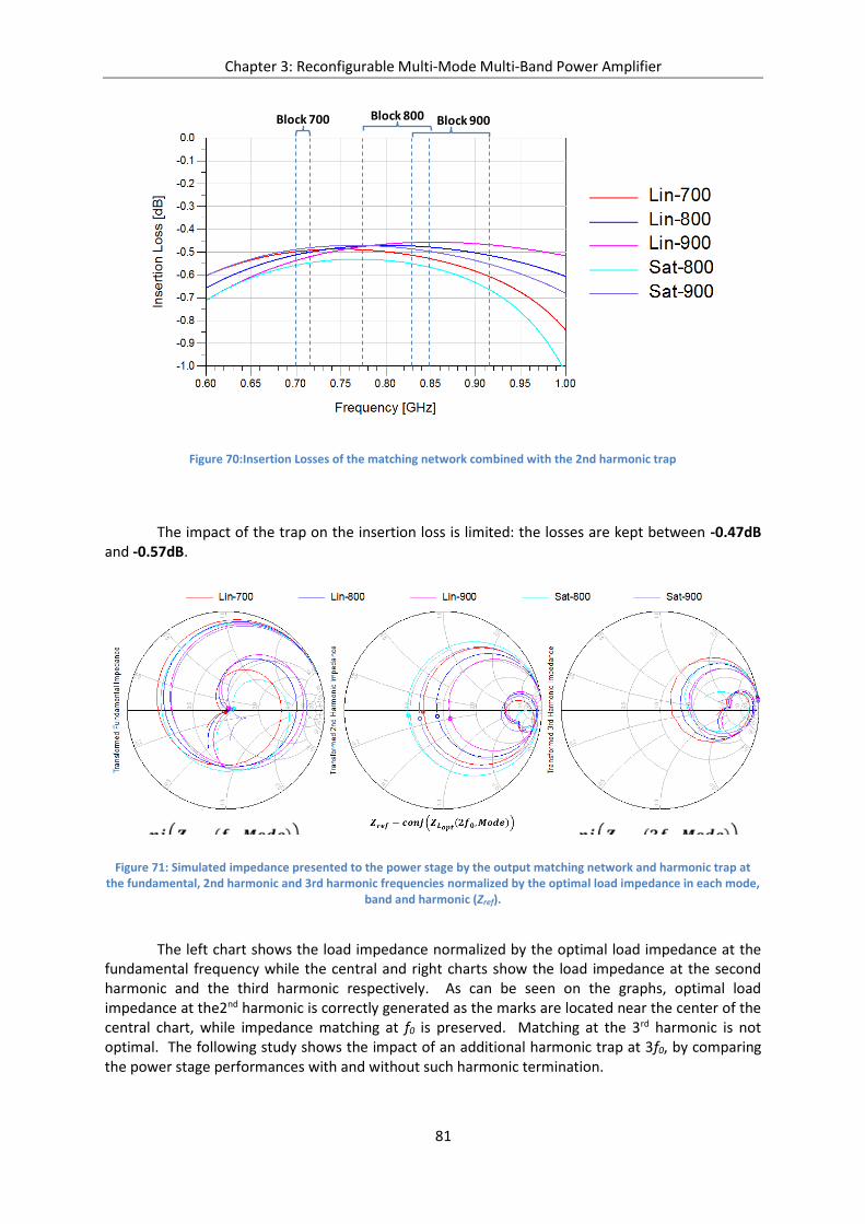
Chapter 3: Reconfigurable Multi-Mode Multi-Band Power Amplifier
81
Figure 70:Insertion Losses of the matching network combined with the 2nd harmonic trap
The impact of the trap on the insertion loss is limited: the losses are kept between -0.47dB and -0.57dB.
Figure 71: Simulated impedance presented to the power stage by the output matching network and harmonic trap at the fundamental, 2nd harmonic and 3rd harmonic frequencies normalized by the optimal load impedance in each mode,
band and harmonic (Zref).
The left chart shows the load impedance normalized by the optimal load impedance at the fundamental frequency while the central and right charts show the load impedance at the second harmonic and the third harmonic respectively. As can be seen on the graphs, optimal load impedance at the2nd harmonic is correctly generated as the marks are located near the center of the central chart, while impedance matching at f0 is preserved. Matching at the 3rd harmonic is not optimal. The following study shows the impact of an additional harmonic trap at 3f0, by comparing the power stage performances with and without such harmonic termination.
Block 900Block 800Block 700
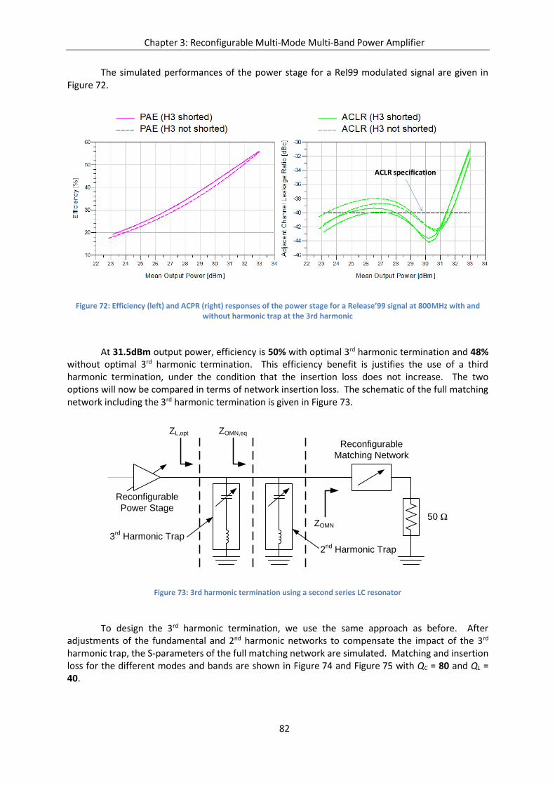
Chapter 3: Reconfigurable Multi-Mode Multi-Band Power Amplifier
82
The simulated performances of the power stage for a Rel99 modulated signal are given in Figure 72.
Figure 72: Efficiency (left) and ACPR (right) responses of the power stage for a Release’99 signal at 800MHz with and without harmonic trap at the 3rd harmonic
At 31.5dBm output power, efficiency is 50% with optimal 3rd harmonic termination and 48% without optimal 3rd harmonic termination. This efficiency benefit is justifies the use of a third harmonic termination, under the condition that the insertion loss does not increase. The two options will now be compared in terms of network insertion loss. The schematic of the full matching network including the 3rd harmonic termination is given in Figure 73.
Figure 73: 3rd harmonic termination using a second series LC resonator
To design the 3rd harmonic termination, we use the same approach as before. After adjustments of the fundamental and 2nd harmonic networks to compensate the impact of the 3rd harmonic trap, the S-parameters of the full matching network are simulated. Matching and insertion loss for the different modes and bands are shown in Figure 74 and Figure 75 with QC = 80 and QL = 40.
ACLR specification
Reconfigurable
Power Stage
Reconfigurable
Matching Network
50 ΩZOMN
ZL,opt
3rd
Harmonic Trap
2nd
Harmonic Trap
ZOMN,eq
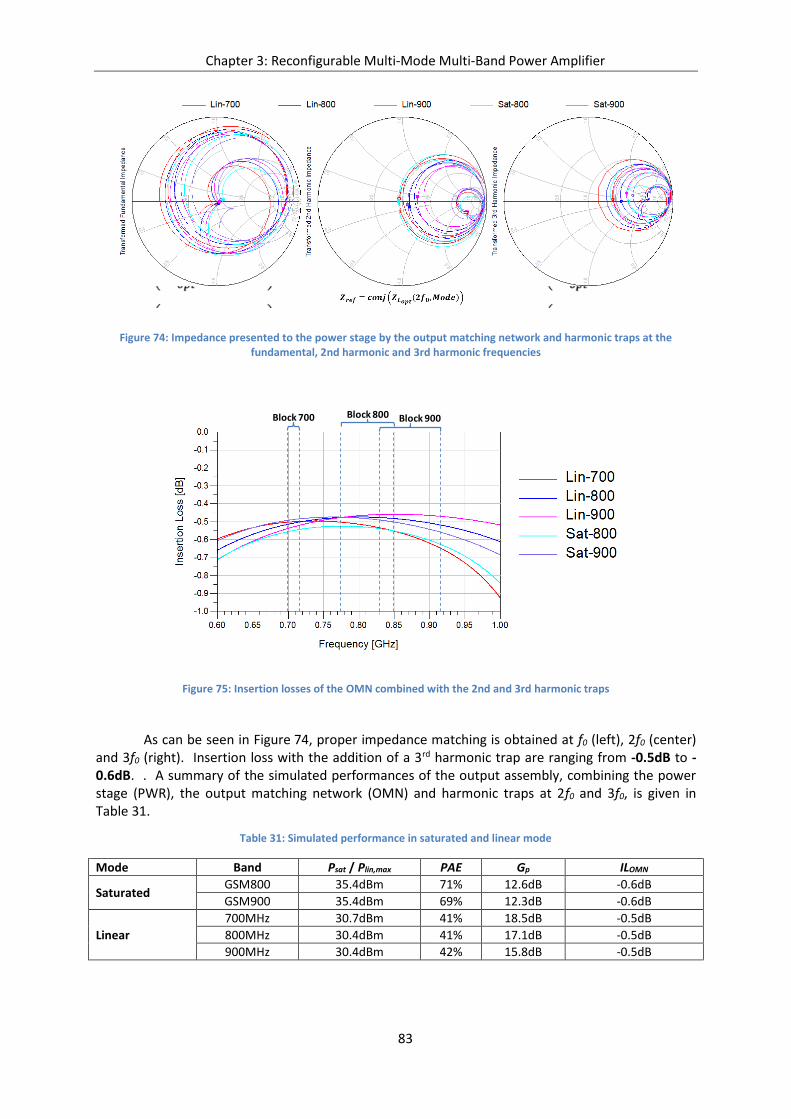
Chapter 3: Reconfigurable Multi-Mode Multi-Band Power Amplifier
83
Figure 74: Impedance presented to the power stage by the output matching network and harmonic traps at the fundamental, 2nd harmonic and 3rd harmonic frequencies
Figure 75: Insertion losses of the OMN combined with the 2nd and 3rd harmonic traps
As can be seen in Figure 74, proper impedance matching is obtained at f0 (left), 2f0 (center) and 3f0 (right). Insertion loss with the addition of a 3rd harmonic trap are ranging from -0.5dB to -0.6dB. . A summary of the simulated performances of the output assembly, combining the power stage (PWR), the output matching network (OMN) and harmonic traps at 2f0 and 3f0, is given in Table 31.
Table 31: Simulated performance in saturated and linear mode
Mode Band Psat / Plin,max PAE Gp ILOMN
Saturated GSM800 35.4dBm 71% 12.6dB -0.6dB
GSM900 35.4dBm 69% 12.3dB -0.6dB
Linear
700MHz 30.7dBm 41% 18.5dB -0.5dB
800MHz 30.4dBm 41% 17.1dB -0.5dB
900MHz 30.4dBm 42% 15.8dB -0.5dB
Block 900Block 800Block 700
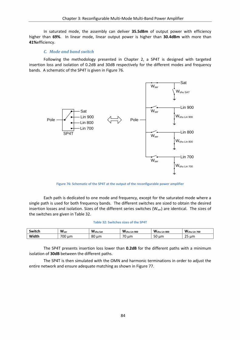
Chapter 3: Reconfigurable Multi-Mode Multi-Band Power Amplifier
84
In saturated mode, the assembly can deliver 35.5dBm of output power with efficiency higher than 69%. In linear mode, linear output power is higher than 30.4dBm with more than 41%efficiency.
C. Mode and band switch
Following the methodology presented in Chapter 2, a SP4T is designed with targeted insertion loss and isolation of 0.2dB and 30dB respectively for the different modes and frequency bands. A schematic of the SP4T is given in Figure 76.
Figure 76: Schematic of the SP4T at the output of the reconfigurable power amplifier
Each path is dedicated to one mode and frequency, except for the saturated mode where a single path is used for both frequency bands. The different switches are sized to obtain the desired insertion losses and isolation. Sizes of the different series switches (Wser) are identical. The sizes of the switches are given in Table 32.
Table 32: Switches sizes of the SP4T
Switch Wser Wshu Sat Wshu Lin 900 Wshu Lin 800 Wshu Lin 700
Width 700 µm 80 µm 70 µm 50 µm 25 µm
The SP4T presents insertion loss lower than 0.2dB for the different paths with a minimum isolation of 30dB between the different paths.
The SP4T is then simulated with the OMN and harmonic terminations in order to adjust the entire network and ensure adequate matching as shown in Figure 77.
Lin 900
Lin 800Pole
SP4T
Lin 700
Sat
Pole
Lin 700Wser
Wshu Lin 700
Lin 800Wser
Wshu Lin 800
Lin 900Wser
Wshu Lin 900
SatWser
Wshu SAT
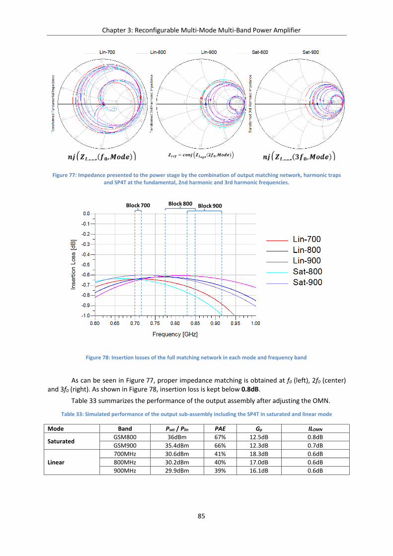
Chapter 3: Reconfigurable Multi-Mode Multi-Band Power Amplifier
85
Figure 77: Impedance presented to the power stage by the combination of output matching network, harmonic traps and SP4T at the fundamental, 2nd harmonic and 3rd harmonic frequencies.
Figure 78: Insertion losses of the full matching network in each mode and frequency band
As can be seen in Figure 77, proper impedance matching is obtained at f0 (left), 2f0 (center) and 3f0 (right). As shown in Figure 78, insertion loss is kept below 0.8dB.
Table 33 summarizes the performance of the output assembly after adjusting the OMN.
Table 33: Simulated performance of the output sub-assembly including the SP4T in saturated and linear mode
Mode Band Psat / Plin PAE Gp ILOMN
Saturated GSM800 36dBm 67% 12.5dB 0.8dB
GSM900 35.4dBm 66% 12.3dB 0.7dB
Linear
700MHz 30.6dBm 41% 18.3dB 0.6dB
800MHz 30.2dBm 40% 17.0dB 0.6dB
900MHz 29.9dBm 39% 16.1dB 0.6dB
Block 900Block 800Block 700
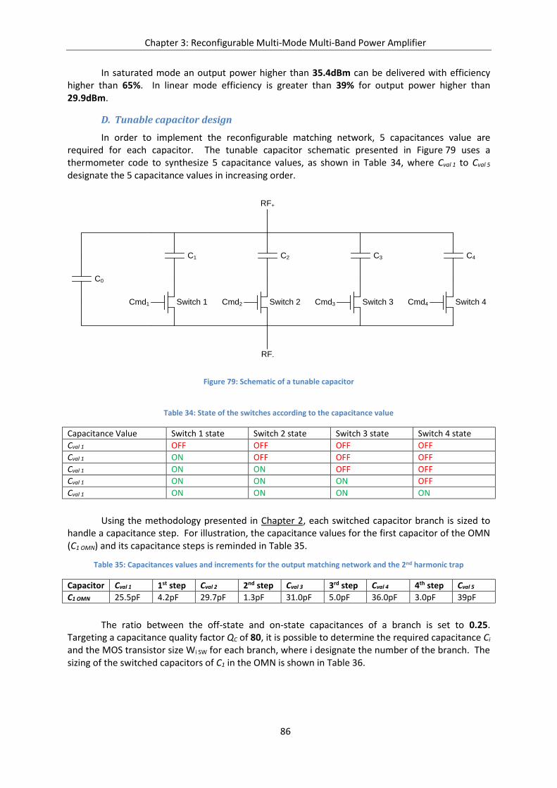
Chapter 3: Reconfigurable Multi-Mode Multi-Band Power Amplifier
86
In saturated mode an output power higher than 35.4dBm can be delivered with efficiency higher than 65%. In linear mode efficiency is greater than 39% for output power higher than 29.9dBm.
D. Tunable capacitor design
In order to implement the reconfigurable matching network, 5 capacitances value are required for each capacitor. The tunable capacitor schematic presented in Figure 79 uses a thermometer code to synthesize 5 capacitance values, as shown in Table 34, where Cval 1 to Cval 5 designate the 5 capacitance values in increasing order.
Figure 79: Schematic of a tunable capacitor
Table 34: State of the switches according to the capacitance value
Capacitance Value Switch 1 state Switch 2 state Switch 3 state Switch 4 state
Cval 1 OFF OFF OFF OFF
Cval 1 ON OFF OFF OFF
Cval 1 ON ON OFF OFF
Cval 1 ON ON ON OFF
Cval 1 ON ON ON ON
Using the methodology presented in Chapter 2, each switched capacitor branch is sized to handle a capacitance step. For illustration, the capacitance values for the first capacitor of the OMN (C1 OMN) and its capacitance steps is reminded in Table 35.
Table 35: Capacitances values and increments for the output matching network and the 2nd harmonic trap
Capacitor Cval 1 1st step Cval 2 2nd step Cval 3 3rd step Cval 4 4th step Cval 5
C1 OMN 25.5pF 4.2pF 29.7pF 1.3pF 31.0pF 5.0pF 36.0pF 3.0pF 39pF
The ratio between the off-state and on-state capacitances of a branch is set to 0.25. Targeting a capacitance quality factor QC of 80, it is possible to determine the required capacitance Ci and the MOS transistor size Wi SW for each branch, where i designate the number of the branch. The sizing of the switched capacitors of C1 in the OMN is shown in Table 36.
C1
Switch 1Cmd1
RF+
RF-
C0
C2
Cmd2
C3
Cmd3
C4
Cmd4Switch 2 Switch 3 Switch 4
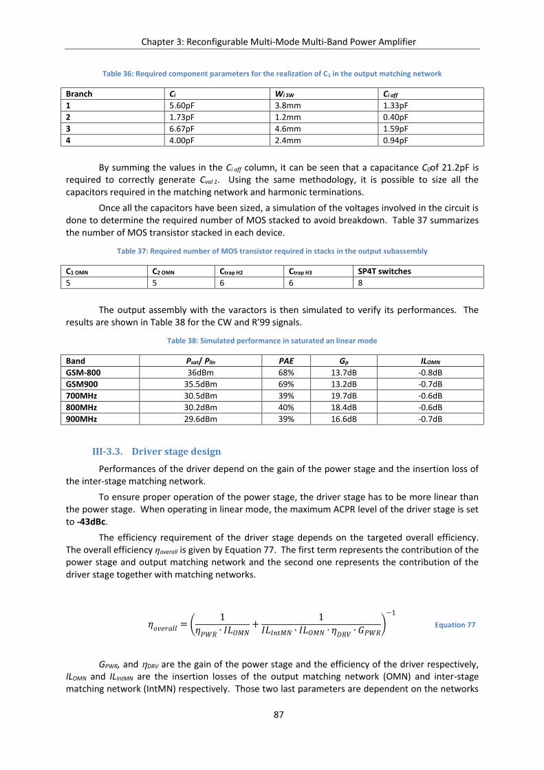
Chapter 3: Reconfigurable Multi-Mode Multi-Band Power Amplifier
87
Table 36: Required component parameters for the realization of C1 in the output matching network
Branch Ci Wi SW Ci off
1 5.60pF 3.8mm 1.33pF
2 1.73pF 1.2mm 0.40pF
3 6.67pF 4.6mm 1.59pF
4 4.00pF 2.4mm 0.94pF
By summing the values in the Ci off column, it can be seen that a capacitance C0of 21.2pF is required to correctly generate Cval 1. Using the same methodology, it is possible to size all the capacitors required in the matching network and harmonic terminations.
Once all the capacitors have been sized, a simulation of the voltages involved in the circuit is done to determine the required number of MOS stacked to avoid breakdown. Table 37 summarizes the number of MOS transistor stacked in each device.
Table 37: Required number of MOS transistor required in stacks in the output subassembly
C1 OMN C2 OMN Ctrap H2 Ctrap H3 SP4T switches
5 5 6 6 8
The output assembly with the varactors is then simulated to verify its performances. The results are shown in Table 38 for the CW and R’99 signals.
Table 38: Simulated performance in saturated an linear mode
Band Psat/ Plin PAE Gp ILOMN
GSM-800 36dBm 68% 13.7dB -0.8dB
GSM900 35.5dBm 69% 13.2dB -0.7dB
700MHz 30.5dBm 39% 19.7dB -0.6dB
800MHz 30.2dBm 40% 18.4dB -0.6dB
900MHz 29.6dBm 39% 16.6dB -0.7dB
III-3.3. Driver stage design
Performances of the driver depend on the gain of the power stage and the insertion loss of the inter-stage matching network.
To ensure proper operation of the power stage, the driver stage has to be more linear than the power stage. When operating in linear mode, the maximum ACPR level of the driver stage is set to -43dBc.
The efficiency requirement of the driver stage depends on the targeted overall efficiency. The overall efficiency ηoverall is given by Equation 77. The first term represents the contribution of the power stage and output matching network and the second one represents the contribution of the driver stage together with matching networks.
GPWR, and DRV are the gain of the power stage and the efficiency of the driver respectively, ILOMN and ILIntMN are the insertion losses of the output matching network (OMN) and inter-stage matching network (IntMN) respectively. Those two last parameters are dependent on the networks
𝜂𝑜𝑣𝑒𝑟𝑎𝑙𝑙 = (1
𝜂𝑃𝑊𝑅 ∙ 𝐼𝐿𝑂𝑀𝑁+
1
𝐼𝐿𝐼𝑛𝑡𝑀𝑁 ∙ 𝐼𝐿𝑂𝑀𝑁 ∙ 𝜂𝐷𝑅𝑉 ∙ 𝐺𝑃𝑊𝑅)
−1
Equation 77
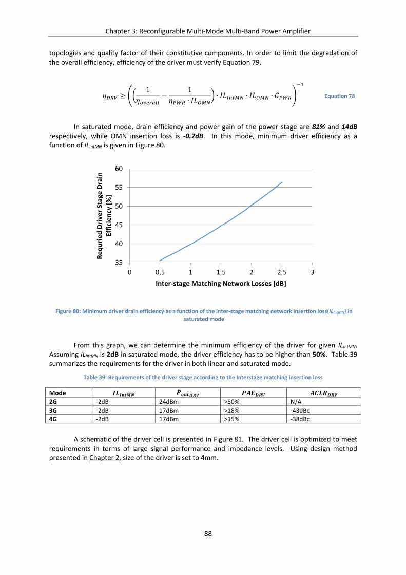
Chapter 3: Reconfigurable Multi-Mode Multi-Band Power Amplifier
88
topologies and quality factor of their constitutive components. In order to limit the degradation of the overall efficiency, efficiency of the driver must verify Equation 79.
𝜂𝐷𝑅𝑉 ≥ ((1
𝜂𝑜𝑣𝑒𝑟𝑎𝑙𝑙−
1
𝜂𝑃𝑊𝑅 ∙ 𝐼𝐿𝑂𝑀𝑁) ∙ 𝐼𝐿𝐼𝑛𝑡𝑀𝑁 ∙ 𝐼𝐿𝑂𝑀𝑁 ∙ 𝐺𝑃𝑊𝑅)
−1
Equation 78
In saturated mode, drain efficiency and power gain of the power stage are 81% and 14dB respectively, while OMN insertion loss is -0.7dB. In this mode, minimum driver efficiency as a function of ILIntMN is given in Figure 80.
Figure 80: Minimum driver drain efficiency as a function of the inter-stage matching network insertion loss(ILIntMN) in saturated mode
From this graph, we can determine the minimum efficiency of the driver for given ILIntMN. Assuming ILIntMN is 2dB in saturated mode, the driver efficiency has to be higher than 50%. Table 39 summarizes the requirements for the driver in both linear and saturated mode.
Table 39: Requirements of the driver stage according to the Interstage matching insertion loss
Mode 𝑰𝑳𝑰𝒏𝒕𝑴𝑵 𝑷𝒐𝒖𝒕𝑫𝑹𝑽 𝑷𝑨𝑬𝑫𝑹𝑽 𝑨𝑪𝑳𝑹𝑫𝑹𝑽
2G -2dB 24dBm >50% N/A
3G -2dB 17dBm >18% -43dBc
4G -2dB 17dBm >15% -38dBc
A schematic of the driver cell is presented in Figure 81. The driver cell is optimized to meet requirements in terms of large signal performance and impedance levels. Using design method presented in Chapter 2, size of the driver is set to 4mm.
35
40
45
50
55
60
0 0,5 1 1,5 2 2,5 3
Re
qu
rie
d D
rive
r St
age
Dra
in
Effi
cien
cy [
%]
Inter-stage Matching Network Losses [dB]
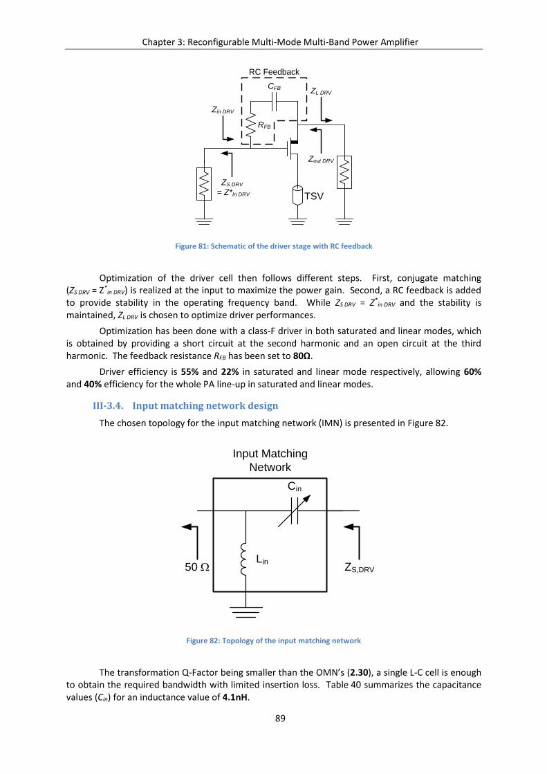
Chapter 3: Reconfigurable Multi-Mode Multi-Band Power Amplifier
89
Figure 81: Schematic of the driver stage with RC feedback
Optimization of the driver cell then follows different steps. First, conjugate matching (ZS DRV = Z*
in DRV) is realized at the input to maximize the power gain. Second, a RC feedback is added to provide stability in the operating frequency band. While ZS DRV = Z*
in DRV and the stability is maintained, ZL DRV is chosen to optimize driver performances.
Optimization has been done with a class-F driver in both saturated and linear modes, which is obtained by providing a short circuit at the second harmonic and an open circuit at the third harmonic. The feedback resistance RFB has been set to 80Ω.
Driver efficiency is 55% and 22% in saturated and linear mode respectively, allowing 60% and 40% efficiency for the whole PA line-up in saturated and linear modes.
III-3.4. Input matching network design
The chosen topology for the input matching network (IMN) is presented in Figure 82.
Lin
Cin
Input Matching
Network
50 W ZS,DRV
Figure 82: Topology of the input matching network
The transformation Q-Factor being smaller than the OMN’s (2.30), a single L-C cell is enough to obtain the required bandwidth with limited insertion loss. Table 40 summarizes the capacitance values (Cin) for an inductance value of 4.1nH.
RFB
CFB
TSV
RC Feedback
ZS DRV
= Z*In DRV
ZL DRV
Zin DRV
Zout DRV
Chapter 3: Reconfigurable Multi-Mode Multi-Band Power Amplifier
90
Table 40: IMN Capacitor value according to the mode for a 4.1nH inductance
Mode Lin-700 Lin-800 Lin-900 Sat-800 Sat-900
Cin 21.0pF 15.7pF 13.5pF 18.0pF 12.0pF
The different capacitance values are obtained through the implementation of a switched capacitor network. The simulated performances are presented in Figure 83.
Figure 83: S11 (left) and insertion loss (right) of the input matching network for the different modes and bands
The simulation results show that the input matching is better than -10dB over the different frequency bands. Maximum insertion loss of the network is less than 0.6dB with QL = 5 and QC=40.
The simulated performances of the driver stage together with the input matching network are given in Table 41.
Table 41: Simulated performance of the driver stage with input matching in saturated and linear modes.
Band Psat/Plin PAE Gp ILIMN
GSM-800 24.4dBm 52% 10.4dB -0.51dB
GSM-900 24.2dBm 51% 10.4dB -0.60dB
700MHz 20.4 33% 12.3dB -0.45dB
800MHz 20.0dBm 31% 12.1dB -0.45dB
900MHz 20.2dBm 32% 12.4dB -0.44dB
In saturated mode, the driver can deliver more than 24dBm of output power with efficiency greater than 50%. In linear mode, the linear output power is greater than 20dBm with more than 30% efficiency.
III-3.5. Inter-stage matching network design
The topology of the inter-stage matching network needs to provide adequate matching between the power stage and the driver stage. Four topologies have been studied as shown in Figure 84.
Band
700
Band
800
Band
900
Chapter 3: Reconfigurable Multi-Mode Multi-Band Power Amplifier
91
Figure 84: Inter-stage matching network topologies.
All those networks are composed of two L-cells, allowing the insertion of two varactors C1 and C2. These four networks are first compared for linear mode at 800MHz in order to decide which topology performs the best for the chosen application. After optimization at 800MHz, the simulated results for the different network configurations in linear mode are given in Figure 85. For the simulation, the quality factor of inductors was set to 10 while the quality factor of capacitors was 80.
Figure 85: Insertion loss (top) and impedances seen at the input (bottom)
To Driver To Power
Topology A
L2
L1 C2
C1
To Driver To Power
Topology C
L2
C2
L1
C1
To Driver To Power
L2L1
C2C1
Topology B
Topology D
To Driver To Power
L2
C2L1
C1
Considered Band
ZL opt DRV
Chapter 3: Reconfigurable Multi-Mode Multi-Band Power Amplifier
92
All topologies except topology C show insertion losses between 2.0dB and 2.2dB in the considered band. Matching at the output of the driver stage varies according to the network topology. The impedances presented by topologies B and C are located on the periphery of the Smith chart and are not well suited. Topologies A and D provide better matching. Topology A has lower losses than topology D but matching presented to the driver stage is better with topology D. Therefore, the topology D is chosen to realize the inter-stage matching network, whose corresponding components values are given in Table 42.
Table 42: Component values of the inter-stage matching network
Mode C1 C2 L1 L2
Lin-700 12pF 55pF
1.65nH 1.25nH Lin-800 7.7pF 45pF
Lin-900 5.0pF 38pF
Sat-800 5.0pF 55pF 1.3nH 0.95nH
Sat-900 3.5pF 45pF
The network requires two inductance values. Tunable inductors are implemented using fixed inductors in parallel with a switched capacitor, see Figure 86.
Figure 86: Implementation of a tunable inductor
When the capacitor is off, the minimum inductance value (Lmin) is obtained. When the capacitor is on, the inductance value is increased to Leq, as defined in Equation 79 where f0 is lower than fres.
𝐿𝑒𝑞 =𝐿𝑚𝑖𝑛
1 − (𝑓0
𝑓𝑟𝑒𝑠)2 where 𝑓𝑟𝑒𝑠 =
1
2𝜋√𝐿𝑚𝑖𝑛𝐶
Equation 79
Using the following equations, the capacitances associated with L1 and L2 are determined.
𝐶 =
1
𝐿𝑚𝑖𝑛 ∙2𝜋𝑓0
√1−𝐿𝑚𝑖𝑛𝐿𝑒𝑞
Equation 80
The required parallel switched capacitors are 6.5pF for L1 and 10pF for L2. C1 and C2 are realized using switched capacitor as previously described.
C
Lmin
RF+RF-
Chapter 3: Reconfigurable Multi-Mode Multi-Band Power Amplifier
93
III-3.6. Reconfigurable MMPA line-up implementation
The reconfigurable MMPA architecture was implemented in a SOI-CMOS 130 nm technology through the design of two circuits, see the block schematic in Figure 87.
Figure 87: Block schematic of the implementation of the MMPA architecture.
The first integrated circuit (IC) includes the power and driver stages, inter-stage and input matching networks, and bias and control circuits (PA IC). The second one (OMN IC) integrates the output matching network including the output SP4T. Both ICs are shown in Figure 88.
Figure 88: Photographs of the two circuits: PA (a) and OMN (b)
The full MMPA test board is depicted in Figure 89.
2G Out
3/4G out 1
3/4G out 2
3/4G out 3
Input
Matching
Driver
Stage
Interstage
Matching
Output
Matching
Cell 1
Cell 2
Power Stage
Analog & Digital Control
Iref,DRV Iref,PWR
5 bits
SPI
VDD,A/D
VDD,DRV VDD,PWR
Analog &
Digital
Control
VDD,A/D
5 bits
SPI
RF in
PA ICOMN IC
(a) (b)
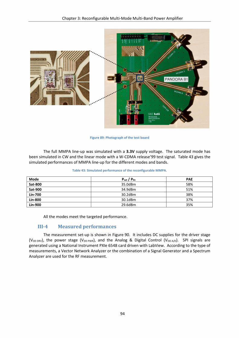
Chapter 3: Reconfigurable Multi-Mode Multi-Band Power Amplifier
94
Figure 89: Photograph of the test board
The full MMPA line-up was simulated with a 3.3V supply voltage. The saturated mode has been simulated in CW and the linear mode with a W-CDMA release’99 test signal. Table 43 gives the simulated performances of MMPA line-up for the different modes and bands.
Table 43: Simulated performance of the reconfigurable MMPA.
Mode Psat / Plin PAE
Sat-800 35.0dBm 58%
Sat-900 34.9dBm 51%
Lin-700 30.2dBm 38%
Lin-800 30.1dBm 37%
Lin-900 29.6dBm 35%
All the modes meet the targeted performance.
III-4 Measured performances
The measurement set-up is shown in Figure 90. It includes DC supplies for the driver stage (VDD DRV), the power stage (VDD PWR), and the Analog & Digital Control (VDD A/D). SPI signals are generated using a National Instrument PXIe 6548 card driven with LabView. According to the type of measurements, a Vector Network Analyzer or the combination of a Signal Generator and a Spectrum Analyzer are used for the RF measurement.
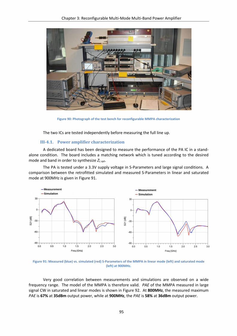
Chapter 3: Reconfigurable Multi-Mode Multi-Band Power Amplifier
95
Figure 90: Photograph of the test bench for reconfigurable MMPA characterization
The two ICs are tested independently before measuring the full line up.
III-4.1. Power amplifier characterization
A dedicated board has been designed to measure the performance of the PA IC in a stand-alone condition. The board includes a matching network which is tuned according to the desired mode and band in order to synthesize ZL opt.
The PA is tested under a 3.3V supply voltage in S-Parameters and large signal conditions. A comparison between the retrofitted simulated and measured S-Parameters in linear and saturated mode at 900MHz is given in Figure 91.
Figure 91: Measured (blue) vs. simulated (red) S-Parameters of the MMPA in linear mode (left) and saturated mode (left) at 900MHz.
Very good correlation between measurements and simulations are observed on a wide frequency range. The model of the MMPA is therefore valid. PAE of the MMPA measured in large signal CW in saturated and linear modes is shown in Figure 92. At 800MHz, the measured maximum PAE is 67% at 35dBm output power, while at 900MHz, the PAE is 58% at 36dBm output power.
Measurement
Simulation
Measurement
Simulation
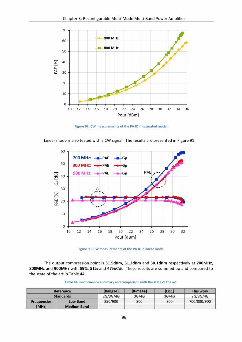
Chapter 3: Reconfigurable Multi-Mode Multi-Band Power Amplifier
96
Figure 92: CW measurements of the PA IC in saturated mode.
Linear mode is also tested with a CW signal. The results are presented in Figure 91.
Figure 93: CW measurements of the PA IC in linear mode.
The output compression point is 31.5dBm, 31.2dBm and 30.1dBm respectively at 700MHz, 800MHz and 900MHz with 59%, 51% and 47%PAE. These results are summed up and compared to the state of the art in Table 44.
Table 44: Performance summary and comparison with the state of the art.
Reference [Kang14] [Kim14a] [Li11] This work
Standards 2G/3G/4G 3G/4G 3G/4G 2G/3G/4G
Frequencies [MHz]
Low Band 850/900 800 800 700/800/900
Medium Band - - -
PAE
GP
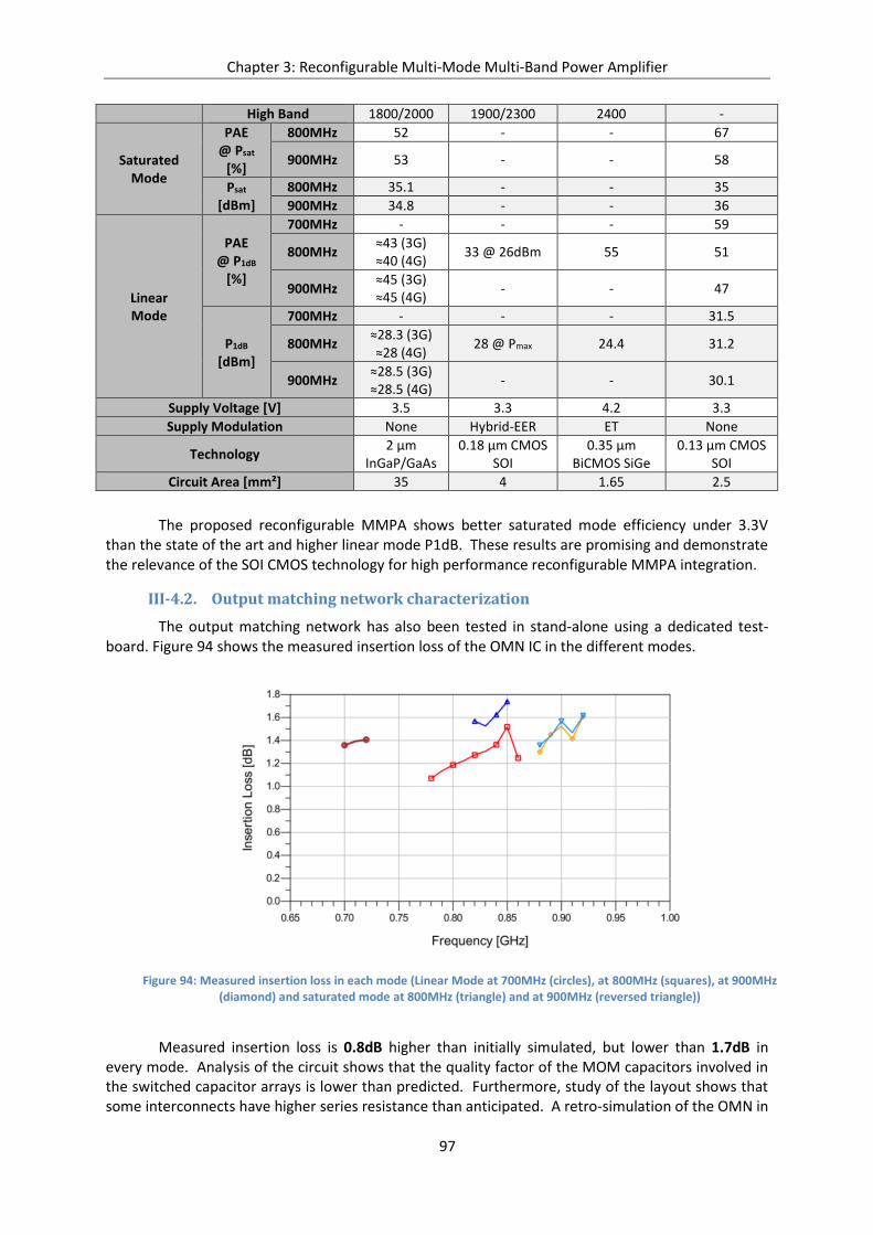
Chapter 3: Reconfigurable Multi-Mode Multi-Band Power Amplifier
97
High Band 1800/2000 1900/2300 2400 -
Saturated Mode
PAE @ Psat
[%]
800MHz 52 - - 67
900MHz 53 - - 58
Psat [dBm]
800MHz 35.1 - - 35
900MHz 34.8 - - 36
Linear Mode
PAE @ P1dB
[%]
700MHz - - - 59
800MHz ≈43 (3G) ≈40 (4G)
33 @ 26dBm 55 51
900MHz ≈45 (3G) ≈45 (4G)
- - 47
P1dB [dBm]
700MHz - - - 31.5
800MHz ≈28.3 (3G) ≈28 (4G)
28 @ Pmax 24.4 31.2
900MHz ≈28.5 (3G) ≈28.5 (4G)
- - 30.1
Supply Voltage [V] 3.5 3.3 4.2 3.3
Supply Modulation None Hybrid-EER ET None
Technology 2 µm
InGaP/GaAs 0.18 µm CMOS
SOI 0.35 µm
BiCMOS SiGe 0.13 µm CMOS
SOI
Circuit Area [mm²] 35 4 1.65 2.5
The proposed reconfigurable MMPA shows better saturated mode efficiency under 3.3V than the state of the art and higher linear mode P1dB. These results are promising and demonstrate the relevance of the SOI CMOS technology for high performance reconfigurable MMPA integration.
III-4.2. Output matching network characterization
The output matching network has also been tested in stand-alone using a dedicated test-board. Figure 94 shows the measured insertion loss of the OMN IC in the different modes.
Measured insertion loss is 0.8dB higher than initially simulated, but lower than 1.7dB in every mode. Analysis of the circuit shows that the quality factor of the MOM capacitors involved in the switched capacitor arrays is lower than predicted. Furthermore, study of the layout shows that some interconnects have higher series resistance than anticipated. A retro-simulation of the OMN in
Figure 94: Measured insertion loss in each mode (Linear Mode at 700MHz (circles), at 800MHz (squares), at 900MHz (diamond) and saturated mode at 800MHz (triangle) and at 900MHz (reversed triangle))
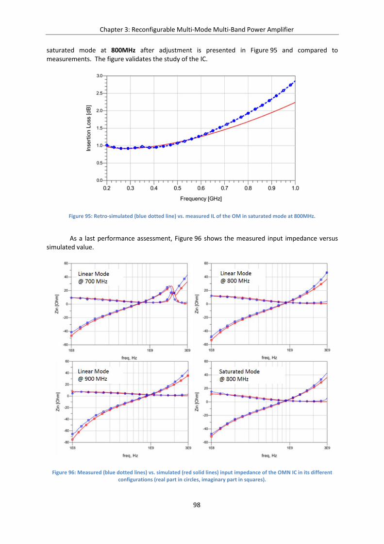
Chapter 3: Reconfigurable Multi-Mode Multi-Band Power Amplifier
98
saturated mode at 800MHz after adjustment is presented in Figure 95 and compared to measurements. The figure validates the study of the IC.
Figure 95: Retro-simulated (blue dotted line) vs. measured IL of the OM in saturated mode at 800MHz.
As a last performance assessment, Figure 96 shows the measured input impedance versus simulated value.
Figure 96: Measured (blue dotted lines) vs. simulated (red solid lines) input impedance of the OMN IC in its different configurations (real part in circles, imaginary part in squares).
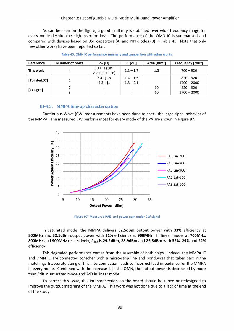
Chapter 3: Reconfigurable Multi-Mode Multi-Band Power Amplifier
99
As can be seen on the figure, a good similarity is obtained over wide frequency range for every mode despite the high insertion loss. The performance of the OMN IC is summarized and compared with devices based on BST capacitors (A) and PIN diodes (B) in Table 45. Note that only few other works have been reported so far.
Table 45: OMN IC performance summary and comparison with other works.
Reference Number of ports Zin [Ω] IL [dB] Area [mm²] Frequency [MHz]
This work 4 1.9 + j1 (Sat.) 2.7 + j0.7 (Lin)
1.1 – 1.7 1.5 700 – 920
[Tombak07] 1 3.4 - j1.9 4.3 + j1
1.4 – 1.6 1.8 – 2.1
820 – 920
1700 – 2000
[Kang15] 2 3
- -
- -
10 10
820 – 920 1700 – 2000
III-4.3. MMPA line-up characterization
Continuous Wave (CW) measurements have been done to check the large signal behavior of the MMPA. The measured CW performances for every mode of the PA are shown in Figure 97.
Figure 97: Measured PAE and power gain under CW signal
In saturated mode, the MMPA delivers 32.5dBm output power with 33% efficiency at 800MHz and 32.1dBm output power with 31% efficiency at 900MHz. In linear mode, at 700MHz, 800MHz and 900MHz respectively, P1dB is 29.2dBm, 28.9dBm and 26.8dBm with 32%, 29% and 22% efficiency.
This degraded performance comes from the assembly of both chips. Indeed, the MMPA IC and OMN IC are connected together with a micro-strip line and bondwires that takes part in the matching. Inaccurate sizing of this interconnection leads to incorrect load impedance for the MMPA in every mode. Combined with the increase IL in the OMN, the output power is decreased by more than 3dB in saturated mode and 2dB in linear mode.
To correct this issue, this interconnection on the board should be tuned or redesigned to improve the output matching of the MMPA. This work was not done due to a lack of time at the end of the study.
0
5
10
15
20
25
30
35
40
5 10 15 20 25 30 35
Po
we
r A
dd
ed
Eff
icie
ncy
[%
]
Output Power [dBm]
PAE Lin-700
PAE Lin-800
PAE Lin-900
PAE Sat-800
PAE Sat-900

Chapter 3: Reconfigurable Multi-Mode Multi-Band Power Amplifier
100
Nonetheless, the previous results show the potential of the 130 nm SOI CMOS process for the design of 2G/3G/4G reconfigurable power amplifiers. With more precise passive and interconnect models, the design process could become more accurate and even better performance could be achieved.
III-5 Conclusion
This chapter has described the design of an integrated SOI CMOS reconfigurable MMPA for the low E-UTRA bands, ranging from 700MHz to 900MHz, for 2G, 3G and 4G standards. The output power stage uses a reconfiguration in size to handle the different requirements of the saturated and the linear modes. The optimal load impedances in each mode and band are synthesized using a reconfigurable output matching network.
The output matching network is actuated using switched capacitor banks. Reconfigurable harmonic terminations are included to optimize the performance of the power stage. A SP4T at the output of the circuit allows routing the signal to the proper output according to the targeted standard and band.
The PA driver is sized according to the performance of the power stage combined with the output matching network. The input matching network and inter-stage matching network were designed using the same methodology as the output matching network. The input matching network uses a simple topology to ensure maximum power transfer to the driver stage. The inter-stage matching network’s topology has been chosen to ensure that the optimal source impedance of the output stage is correctly generated while ensuring proper operation of the driver stage.
The bias circuit is optimized to provide low baseband impedance to the stages, thus limiting the memory effects.
The power amplifier was implemented in 2 integrated circuits. The power amplifier circuit shows performance at the state of the art in terms of output power and efficiency.
The output matching circuit provides the targeted impedances, for a lower surface when compared to the literature. Lower quality factor in MOM capacitors and higher resistance in interconnections however translates in insertion losses slightly higher than expected. This was demonstrated by post-simulations.
The full assembly is composed of both integrated circuits mounted on test board. It suffers from the insertion loss issues in the output matching circuit. The performance is also decreased due to imprecision in the combining line implemented on the board which participates in synthesizing the optimal load impedance of the power stage. Nonetheless, output powersof30dBm in linear mode and 32dBm in saturated mode have been measured. The chosen technology is therefore considered as a promising candidate for integrating reconfigurable MMPA. Further investigation on the assembly of the two circuits and improved layout of the output matching network could help reaching the targeted performance.
The next chapter describes PA architectures to improve efficiency.
Chapter 3: Reconfigurable Multi-Mode Multi-Band Power Amplifier
101
III-6 References
[Ali10] F. Ali and E. Lourandakis, “Tunable Multiband Power Amplifier using Thin-Film BST Varactors for 4G Handheld Applications”, IEEE Radio and Wireless Symposium digest, pp. 236-239, 2010.
[Chalermwisutkul08] S. Chalermwisutkul, “Phenomena of Electrical Memory Effects on the Device Level and Their Relations”, IEEE Electronics, Computer, Telecommunications and Information Technology Conf. Proceed. Dig., pp. 229-232, May 2008.
[Kang14] S. Kang, U. Kim, & J. Kim, “A Multi-Mode Multi-Band Reconfigurable Power Amplifier for 2G/3G/4G Handset Applications”, IEEE Microwave and Wireless Component Letters, pp. 49-51, 2014.
[Kim14] U. Kim, S. Kang, J. Kim and Y. Kwon, “A Fully-Integrated Penta-Band Tx Reconfigurable Power Amplifier with SOI CMOS Switches for Mobile Handset Applications”, ETRI Journal, vol. 36, no. 2, pp. 214-223, April 2014.
[Kim14a] W.-Y. Kim, H. S. Son, J. Y. Jang, J. H. Kim, I. Y. Oh and C. S. Park, “A fully integrated triple-band CMOS hybrid-EER transmitter for WCDMA.LTE applications”, IEEE Microwave Theory and Technique Symposium Digest, pp. 1-3, June 2014.
[Li11] Y. Li, J. Lopez, P.-H. Wu, W. Hu, R. Wu and D. Y. C. Lie, “A SiGe envelope modulator for mobile WiMAX/3GPP LTE transmitters”, IEEE Transactions on Microwave Theory and Techniques, vol. 59, pp. 2525-2536, October 2011.
[Mori00] K. Mori, S. Shinjo, F. Kitabayashi, A. Ohta, Y. Ikeda & O. Ishida, “An L-Band High Efficiency and Low-Distortion Power Amplifier Using HPF/LPF Combined Interstage Matching Circuit”, IEEE Transactions on Microwave Theory and Techniques, vol. 48, pp. 2560-2566, December 2000.
[Park14] S. Park, J.-L. Woo, M.-S. Jeaon, U. Kim and Y. Kwon, “Broadband CMOS Stacked Power Amplifier Using Reconfigurable Interstage Network for Envelope Tracking Application”, IEEE Radio Frequency Integrated Circuit Symposium digest, pp. 145-148, 2014.
[Pornpromlikit10] S. Pornpromlikit, J. Jeong, C. D. Presti, A. Scuderi and P. M. Asbeck, “A Watt-Level Stacked-FET Linear Power Amplifier in Silicon-on-Insulator CMOS”, IEEE Transactions on Microwave Theory and Techniques, vol. 58, pp. 57-646, January 2010.
[Tombak07] A. Tombak, “A ferroelectric-capacitor-based tunable matching network for quad band cellular power amplifiers”, IEEE Transactions on Microwave Theory and Techniques, vol. 55, pp. 370-375, February 2007.
[Yin14] Y. Yin, B. Chi, Z. Xia and Z. Zhihua, “A Reconfigurable Dual-Mode CMOS Power Amplifier with Integrated T/R Switch for 0.1—1.5-GHz Multistandard Applications”, IEEE Transactions on Circuits and Systems—II: Express Briefs, vol. 61, pp. 471-475, July 2014.

Chapter 3: Reconfigurable Multi-Mode Multi-Band Power Amplifier
102
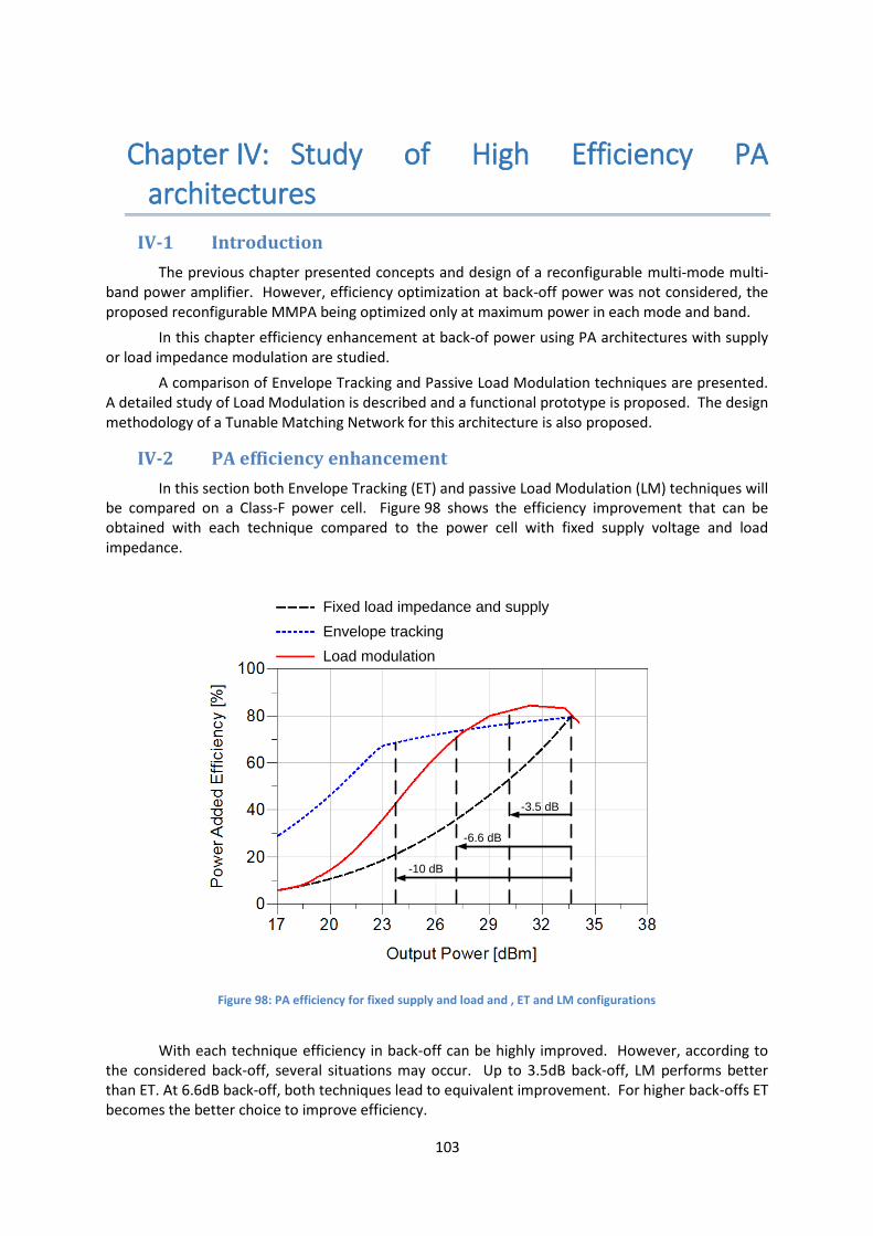
103
Chapter IV: Study of High Efficiency PA architectures
IV-1 Introduction
The previous chapter presented concepts and design of a reconfigurable multi-mode multi-band power amplifier. However, efficiency optimization at back-off power was not considered, the proposed reconfigurable MMPA being optimized only at maximum power in each mode and band.
In this chapter efficiency enhancement at back-of power using PA architectures with supply or load impedance modulation are studied.
A comparison of Envelope Tracking and Passive Load Modulation techniques are presented. A detailed study of Load Modulation is described and a functional prototype is proposed. The design methodology of a Tunable Matching Network for this architecture is also proposed.
IV-2 PA efficiency enhancement
In this section both Envelope Tracking (ET) and passive Load Modulation (LM) techniques will be compared on a Class-F power cell. Figure 98 shows the efficiency improvement that can be obtained with each technique compared to the power cell with fixed supply voltage and load impedance.
Figure 98: PA efficiency for fixed supply and load and , ET and LM configurations
With each technique efficiency in back-off can be highly improved. However, according to the considered back-off, several situations may occur. Up to 3.5dB back-off, LM performs better than ET. At 6.6dB back-off, both techniques lead to equivalent improvement. For higher back-offs ET becomes the better choice to improve efficiency.
-3.5 dB
-6.6 dB
-10 dB
Fixed load impedance and supply
Envelope tracking
Load modulation
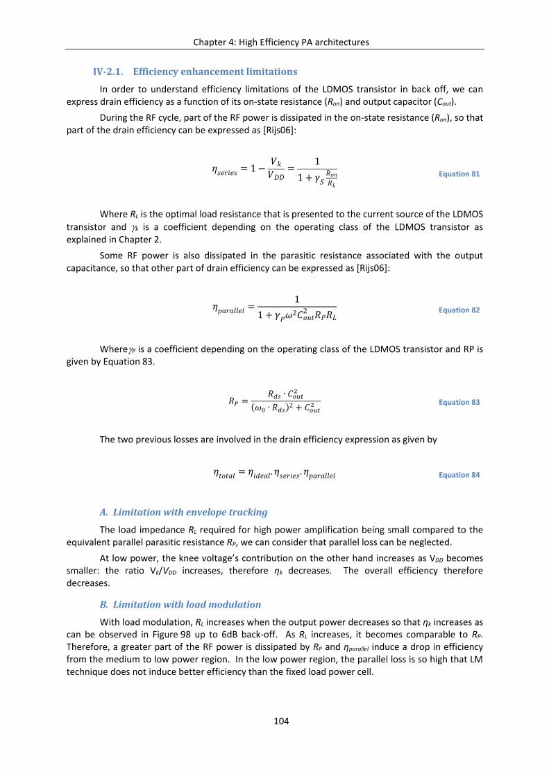
Chapter 4: High Efficiency PA architectures
104
IV-2.1. Efficiency enhancement limitations
In order to understand efficiency limitations of the LDMOS transistor in back off, we can express drain efficiency as a function of its on-state resistance (Ron) and output capacitor (Cout).
During the RF cycle, part of the RF power is dissipated in the on-state resistance (Ron), so that part of the drain efficiency can be expressed as [Rijs06]:
𝜂𝑠𝑒𝑟𝑖𝑒𝑠 = 1−𝑉𝑘𝑉𝐷𝐷
=1
1 + 𝛾𝑆𝑅𝑜𝑛𝑅𝐿
Equation 81
Where RL is the optimal load resistance that is presented to the current source of the LDMOS
transistor and k is a coefficient depending on the operating class of the LDMOS transistor as explained in Chapter 2.
Some RF power is also dissipated in the parasitic resistance associated with the output capacitance, so that other part of drain efficiency can be expressed as [Rijs06]:
𝜂𝑝𝑎𝑟𝑎𝑙𝑙𝑒𝑙 =1
1 + 𝛾𝑃𝜔2𝐶𝑜𝑢𝑡
2 𝑅𝑃𝑅𝐿 Equation 82
WhereP is a coefficient depending on the operating class of the LDMOS transistor and RP is given by Equation 83.
𝑅𝑃 =𝑅𝑑𝑠 ∙ 𝐶𝑜𝑢𝑡
2
(𝜔0 ∙ 𝑅𝑑𝑠)2 + 𝐶𝑜𝑢𝑡
2 Equation 83
The two previous losses are involved in the drain efficiency expression as given by
𝜂𝑡𝑜𝑡𝑎𝑙 = 𝜂𝑖𝑑𝑒𝑎𝑙. 𝜂𝑠𝑒𝑟𝑖𝑒𝑠. 𝜂𝑝𝑎𝑟𝑎𝑙𝑙𝑒𝑙 Equation 84
A. Limitation with envelope tracking
The load impedance RL required for high power amplification being small compared to the equivalent parallel parasitic resistance RP, we can consider that parallel loss can be neglected.
At low power, the knee voltage’s contribution on the other hand increases as VDD becomes smaller: the ratio Vk/VDD increases, therefore ηk decreases. The overall efficiency therefore decreases.
B. Limitation with load modulation
With load modulation, RL increases when the output power decreases so that ηk increases as can be observed in Figure 98 up to 6dB back-off. As RL increases, it becomes comparable to RP. Therefore, a greater part of the RF power is dissipated by RP and ηparallel induce a drop in efficiency from the medium to low power region. In the low power region, the parallel loss is so high that LM technique does not induce better efficiency than the fixed load power cell.
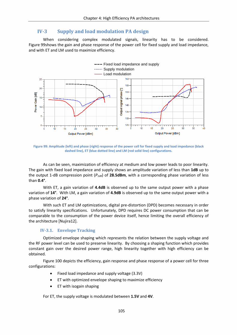
Chapter 4: High Efficiency PA architectures
105
IV-3 Supply and load modulation PA design
When considering complex modulated signals, linearity has to be considered. Figure 99shows the gain and phase response of the power cell for fixed supply and load impedance, and with ET and LM used to maximize efficiency.
Figure 99: Amplitude (left) and phase (right) response of the power cell for fixed supply and load impedance (black dashed line), ET (blue dotted line) and LM (red solid line) configurations.
As can be seen, maximization of efficiency at medium and low power leads to poor linearity. The gain with fixed load impedance and supply shows an amplitude variation of less than 1dB up to the output 1-dB compression point (P1dB) of 28.5dBm, with a corresponding phase variation of less than 0.4°.
With ET, a gain variation of 4.4dB is observed up to the same output power with a phase variation of 14°. With LM, a gain variation of 4.9dB is observed up to the same output power with a phase variation of 24°.
With such ET and LM optimizations, digital pre-distortion (DPD) becomes necessary in order to satisfy linearity specifications. Unfortunately, DPD requires DC power consumption that can be comparable to the consumption of the power device itself, hence limiting the overall efficiency of the architecture [Nujira12].
IV-3.1. Envelope Tracking
Optimized envelope shaping which represents the relation between the supply voltage and the RF power level can be used to preserve linearity. By choosing a shaping function which provides constant gain over the desired power range, high linearity together with high efficiency can be obtained.
Figure 100 depicts the efficiency, gain response and phase response of a power cell for three configurations:
Fixed load impedance and supply voltage (3.3V)
ET with optimized envelope shaping to maximize efficiency
ET with isogain shaping
For ET, the supply voltage is modulated between 1.5V and 4V.
Fixed load impedance and supply
Supply modulation
Load modulation
Chapter 4: High Efficiency PA architectures
106
Figure 100: Efficiency (top left), gain (bottom left) and phase (bottom right) comparison between the stand alone cell, ET power cell with maximum efficiency shaping and ET power cell with isogain shaping.
Envelope information which is extracted using an envelope detector is transferred to an envelope shaping block where the detected envelope power is compared to the power levels stored in a shaping data file. The corresponding supply voltage is then applied to the power cell. In order to quantify the achievable PAE improvement, the power cell using ET with isogain shaping (ET cell) is compared to the fixed supply cell for 3G (Figure 101) and 4G (Figure 102) signals
Fixed load impedance and supply
Maximized PAE shaping
Isogain shaping
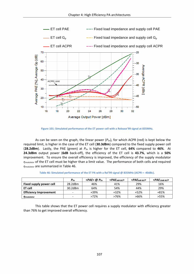
Chapter 4: High Efficiency PA architectures
107
Figure 101: Simulated performance of the ET power cell with a Release’99 signal at 835MHz.
As can be seen on the graph, the linear power (Plin), for which ACPR (red) is kept below the required limit, is higher in the case of the ET cell (30.3dBm) compared to the fixed supply power cell (28.2dBm). Lastly, the PAE (green) at Plin is higher for the ET cell, 64% compared to 46%. At 24.3dBm output power (6dB back-off), the efficiency of the ET cell is 43.7%, which is a 50% improvement. To ensure the overall efficiency is improved, the efficiency of the supply modulator ηmodulator of the ET cell must be higher than a limit value. The performance of both cells and required ηmodulator are summarized in Table 46.
Table 46: Simulated performance of the ET PA with a Rel'99 signal @ 835MHz (ACPR = -40dBc).
Plin <PAE> @ Plin <PAE3dB BO> <PAE6dB BO> <PAE10dB BO>
Fixed supply power cell 28.2dBm 46% 41% 29% 16%
ET cell 30.2dBm 64% 54% 44% 29%
Efficiency Improvement - +39% +32% +52% +81%
ηmodulator - >72% >76% >66% >55%
This table shows that the ET power cell requires a supply modulator with efficiency greater than 76% to get improved overall efficiency.
Fixed load impedance and supply cell PAE
Fixed load impedance and supply cell Gp
Fixed load impedance and supply cell ACPR
ET cell PAE
ET cell Gp
ET cell ACPR
ACPR Limit
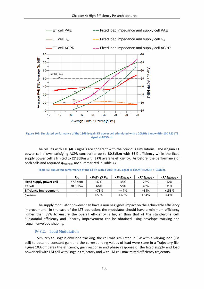
Chapter 4: High Efficiency PA architectures
108
Figure 102: Simulated performance of the 18dB Isogain ET power cell stimulated with a 20MHz bandwidth (100 RB) LTE signal at 835MHz.
The results with LTE (4G) signals are coherent with the previous simulations. The isogain ET power cell allows satisfying ACPR constraints up to 30.5dBm with 66% efficiency while the fixed supply power cell is limited to 27.3dBm with 37% average efficiency. As before, the performance of both cells and required ηmodulator are summarized in Table 47.
Table 47: Simulated performance of the ET PA with a 20MHz LTE signal @ 835MHz (ACPR = -35dBc).
Plin <PAE> @ Plin <PAE3dB BO> <PAE6dB BO> <PAE10dB BO>
Fixed supply power cell 27.3dBm 37% 38% 25% 12%
ET cell 30.5dBm 66% 56% 46% 31%
Efficiency Improvement - +78% +47% +84% +158%
ηmodulator - >56% >68% >54% >39%
The supply modulator however can have a non negligible impact on the achievable efficiency improvement. In the case of the LTE operation, the modulator should have a minimum efficiency higher than 68% to ensure the overall efficiency is higher than that of the stand-alone cell. Substantial efficiency and linearity improvement can be obtained using envelope tracking and isogain envelope shaping.
IV-3.2. Load Modulation
Similarly to isogain envelope tracking, the cell was simulated in CW with a varying load (LM cell) to obtain a constant gain and the corresponding values of load were store in a Trajectory file. Figure 103compares the efficiency, gain response and phase response of the fixed supply and load power cell with LM cell with isogain trajectory and with LM cell maximized efficiency trajectory.
Fixed load impedance and supply cell PAE
Fixed load impedance and supply cell Gp
Fixed load impedance and supply cell ACPR
ET cell PAE
ET cell Gp
ET cell ACPR
ACPR Limit
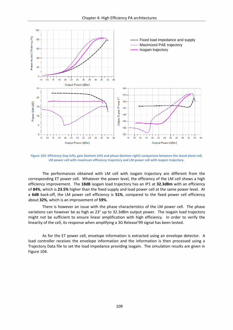
Chapter 4: High Efficiency PA architectures
109
Figure 103: Efficiency (top left), gain (bottom left) and phase (bottom right) comparison between the stand alone cell, LM power cell with maximum efficiency trajectory and LM power cell with isogain trajectory.
The performances obtained with LM cell with isogain trajectory are different from the corresponding ET power cell. Whatever the power level, the efficiency of the LM cell shows a high efficiency improvement. The 18dB isogain load trajectory has an IP1 at 32.3dBm with an efficiency of 84%, which is 23.5% higher than the fixed supply and load power cell at the same power level. At a 6dB back-off, the LM power cell efficiency is 51%, compared to the fixed power cell efficiency about 32%, which is an improvement of 59%.
There is however an issue with the phase characteristics of the LM power cell. The phase variations can however be as high as 23° up to 32.3dBm output power. The isogain load trajectory might not be sufficient to ensure linear amplification with high efficiency. In order to verify the linearity of the cell, its response when amplifying a 3G Release’99 signal has been tested.
As for the ET power cell, envelope information is extracted using an envelope detector. A load controller receives the envelope information and the information is then processed using a Trajectory Data file to set the load impedance providing isogain. The simulation results are given in Figure 104.
Fixed load impedance and supply
Maximized PAE trajectory
Isogain trajectory
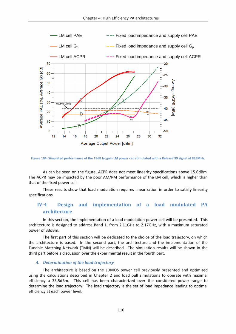
Chapter 4: High Efficiency PA architectures
110
Figure 104: Simulated performance of the 18dB Isogain LM power cell stimulated with a Release’99 signal at 835MHz.
As can be seen on the figure, ACPR does not meet linearity specifications above 15.6dBm. The ACPR may be impacted by the poor AM/PM performance of the LM cell, which is higher than that of the fixed power cell.
These results show that load modulation requires linearization in order to satisfy linearity specifications.
IV-4 Design and implementation of a load modulated PA
architecture
In this section, the implementation of a load modulation power cell will be presented. This architecture is designed to address Band 1, from 2.11GHz to 2.17GHz, with a maximum saturated power of 33dBm.
The first part of this section will be dedicated to the choice of the load trajectory, on which the architecture is based. In the second part, the architecture and the implementation of the Tunable Matching Network (TMN) will be described. The simulation results will be shown in the third part before a discussion over the experimental result in the fourth part.
A. Determination of the load trajectory
The architecture is based on the LDMOS power cell previously presented and optimized using the calculations described in Chapter 2 and load pull simulations to operate with maximal efficiency a 33.5dBm. This cell has been characterized over the considered power range to determine the load trajectory. The load trajectory is the set of load impedance leading to optimal efficiency at each power level.
Fixed load impedance and supply cell PAE
Fixed load impedance and supply cell Gp
Fixed load impedance and supply cell ACPR
LM cell PAE
LM cell Gp
LM cell ACPR
ACPR Limit
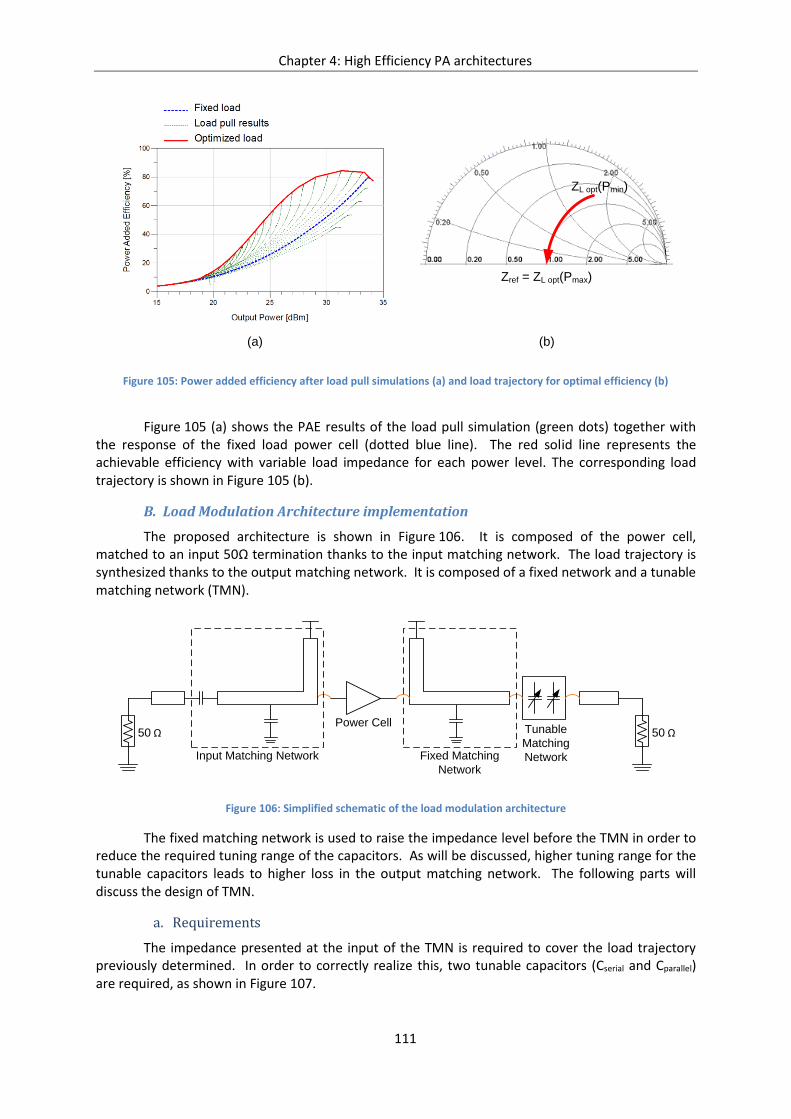
Chapter 4: High Efficiency PA architectures
111
Figure 105: Power added efficiency after load pull simulations (a) and load trajectory for optimal efficiency (b)
Figure 105 (a) shows the PAE results of the load pull simulation (green dots) together with the response of the fixed load power cell (dotted blue line). The red solid line represents the achievable efficiency with variable load impedance for each power level. The corresponding load trajectory is shown in Figure 105 (b).
B. Load Modulation Architecture implementation
The proposed architecture is shown in Figure 106. It is composed of the power cell, matched to an input 50Ω termination thanks to the input matching network. The load trajectory is synthesized thanks to the output matching network. It is composed of a fixed network and a tunable matching network (TMN).
Figure 106: Simplified schematic of the load modulation architecture
The fixed matching network is used to raise the impedance level before the TMN in order to reduce the required tuning range of the capacitors. As will be discussed, higher tuning range for the tunable capacitors leads to higher loss in the output matching network. The following parts will discuss the design of TMN.
a. Requirements
The impedance presented at the input of the TMN is required to cover the load trajectory previously determined. In order to correctly realize this, two tunable capacitors (Cserial and Cparallel) are required, as shown in Figure 107.
Zref = ZL opt(Pmax)
ZL opt(Pmin)
(a) (b)
Fixed Matching
Network
Tunable
Matching
Network
Power Cell
Input Matching Network
50 Ω50 Ω
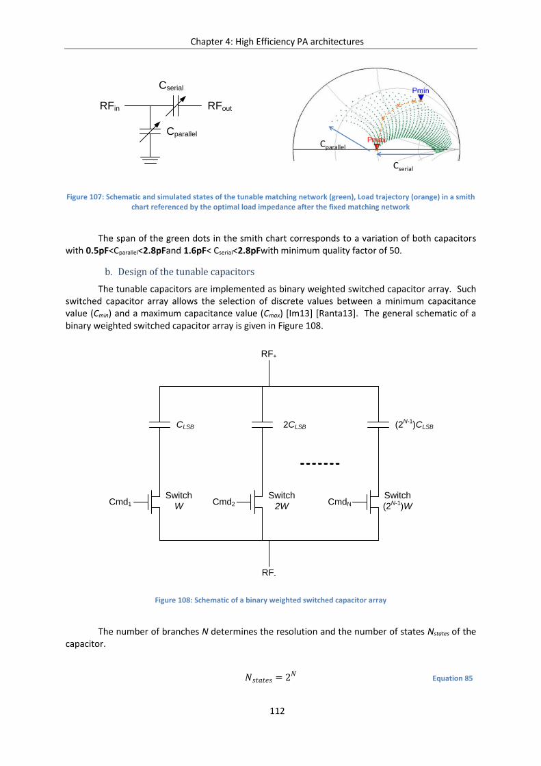
Chapter 4: High Efficiency PA architectures
112
Figure 107: Schematic and simulated states of the tunable matching network (green), Load trajectory (orange) in a smith chart referenced by the optimal load impedance after the fixed matching network
The span of the green dots in the smith chart corresponds to a variation of both capacitors with 0.5pF<Cparallel<2.8pFand 1.6pF< Cserial<2.8pFwith minimum quality factor of 50.
b. Design of the tunable capacitors
The tunable capacitors are implemented as binary weighted switched capacitor array. Such switched capacitor array allows the selection of discrete values between a minimum capacitance value (Cmin) and a maximum capacitance value (Cmax) [Im13] [Ranta13]. The general schematic of a binary weighted switched capacitor array is given in Figure 108.
Figure 108: Schematic of a binary weighted switched capacitor array
The number of branches N determines the resolution and the number of states Nstates of the capacitor.
𝑁𝑠𝑡𝑎𝑡𝑒𝑠 = 2𝑁
Equation 85
Cparallel
Cserial
RFoutRFin
Cserial
Cparallel
CLSB
Switch
WCmd1
2CLSB
Switch
2W
RF+
RF-
Cmd2
(2N-1
)CLSB
Switch
(2N-1
)WCmdN
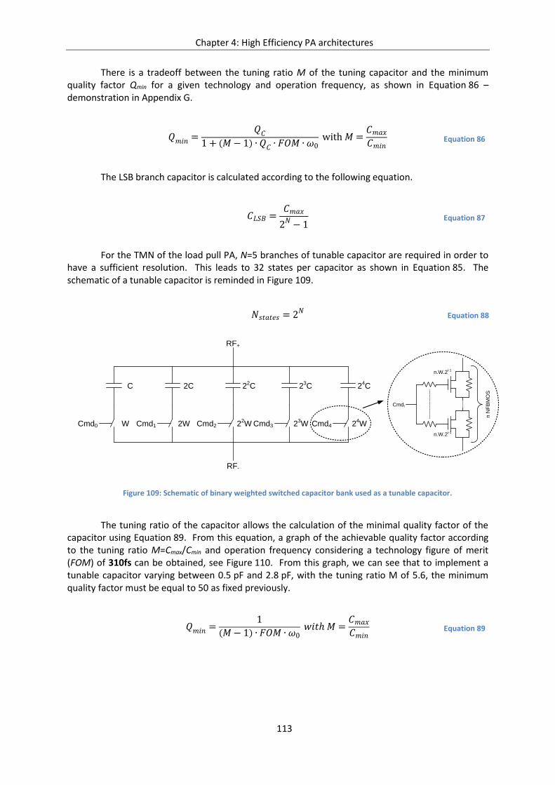
Chapter 4: High Efficiency PA architectures
113
There is a tradeoff between the tuning ratio M of the tuning capacitor and the minimum quality factor Qmin for a given technology and operation frequency, as shown in Equation 86 –demonstration in Appendix G.
𝑄𝑚𝑖𝑛 =𝑄𝐶
1 + (𝑀−1) ∙ 𝑄𝐶 ∙ 𝐹𝑂𝑀 ∙ 𝜔0 with 𝑀 =
𝐶𝑚𝑎𝑥𝐶𝑚𝑖𝑛
Equation 86
The LSB branch capacitor is calculated according to the following equation.
𝐶𝐿𝑆𝐵 =𝐶𝑚𝑎𝑥
2𝑁 − 1 Equation 87
For the TMN of the load pull PA, N=5 branches of tunable capacitor are required in order to have a sufficient resolution. This leads to 32 states per capacitor as shown in Equation 85. The schematic of a tunable capacitor is reminded in Figure 109.
𝑁𝑠𝑡𝑎𝑡𝑒𝑠 = 2𝑁
Equation 88
Figure 109: Schematic of binary weighted switched capacitor bank used as a tunable capacitor.
The tuning ratio of the capacitor allows the calculation of the minimal quality factor of the capacitor using Equation 89. From this equation, a graph of the achievable quality factor according to the tuning ratio M=Cmax/Cmin and operation frequency considering a technology figure of merit (FOM) of 310fs can be obtained, see Figure 110. From this graph, we can see that to implement a tunable capacitor varying between 0.5 pF and 2.8 pF, with the tuning ratio M of 5.6, the minimum quality factor must be equal to 50 as fixed previously.
𝑄𝑚𝑖𝑛 =1
(𝑀−1) ∙ 𝐹𝑂𝑀 ∙ 𝜔0 𝑤𝑖𝑡ℎ 𝑀 =
𝐶𝑚𝑎𝑥𝐶𝑚𝑖𝑛
Equation 89
n N
FB
MO
S
Cmdi
n.W.2i-1
n.W.2i-1
RF+
RF-
C
Cmd0 W
2C
Cmd1 2W
22C
Cmd2 22W
23C
Cmd3 23W
24C
Cmd4 24W
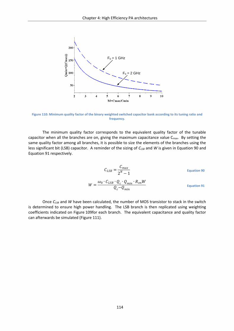
Chapter 4: High Efficiency PA architectures
114
Figure 110: Minimum quality factor of the binary weighted switched capacitor bank according to its tuning ratio and frequency.
The minimum quality factor corresponds to the equivalent quality factor of the tunable capacitor when all the branches are on, giving the maximum capacitance value Cmax. By setting the same quality factor among all branches, it is possible to size the elements of the branches using the less significant bit (LSB) capacitor. A reminder of the sizing of CLSB and W is given in Equation 90 and Equation 91 respectively.
𝐶𝐿𝑆𝐵 =𝐶𝑚𝑎𝑥
2𝑁 − 1 Equation 90
𝑊 =𝜔0 ∙ 𝐶𝐿𝑆𝐵 ∙ 𝑄𝑐 ∙ 𝑄𝑚𝑖𝑛 ∙ 𝑅𝑜𝑛𝑊
𝑄𝑐−𝑄𝑚𝑖𝑛 Equation 91
Once CLSB and W have been calculated, the number of MOS transistor to stack in the switch is determined to ensure high power handling. The LSB branch is then replicated using weighting coefficients indicated on Figure 109for each branch. The equivalent capacitance and quality factor can afterwards be simulated (Figure 111).
F0 = 1 GHz
F0 = 2 GHz
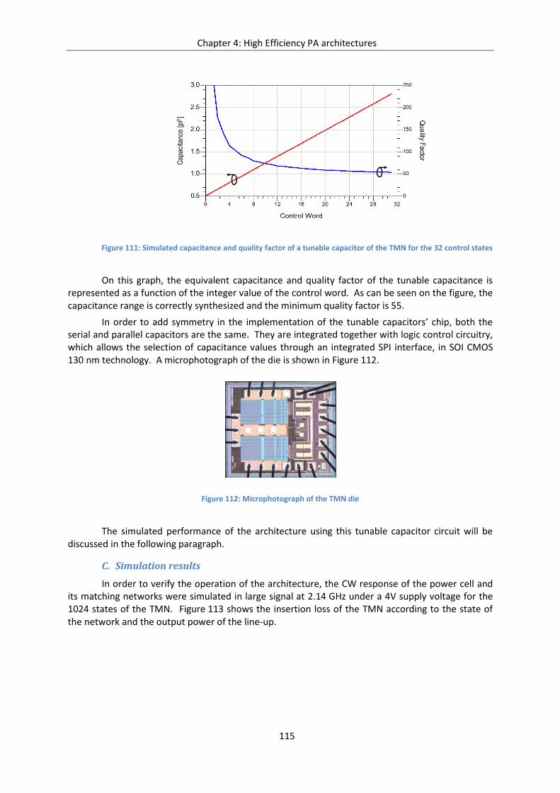
Chapter 4: High Efficiency PA architectures
115
On this graph, the equivalent capacitance and quality factor of the tunable capacitance is represented as a function of the integer value of the control word. As can be seen on the figure, the capacitance range is correctly synthesized and the minimum quality factor is 55.
In order to add symmetry in the implementation of the tunable capacitors’ chip, both the serial and parallel capacitors are the same. They are integrated together with logic control circuitry, which allows the selection of capacitance values through an integrated SPI interface, in SOI CMOS 130 nm technology. A microphotograph of the die is shown in Figure 112.
Figure 112: Microphotograph of the TMN die
The simulated performance of the architecture using this tunable capacitor circuit will be discussed in the following paragraph.
C. Simulation results
In order to verify the operation of the architecture, the CW response of the power cell and its matching networks were simulated in large signal at 2.14 GHz under a 4V supply voltage for the 1024 states of the TMN. Figure 113 shows the insertion loss of the TMN according to the state of the network and the output power of the line-up.
Figure 111: Simulated capacitance and quality factor of a tunable capacitor of the TMN for the 32 control states
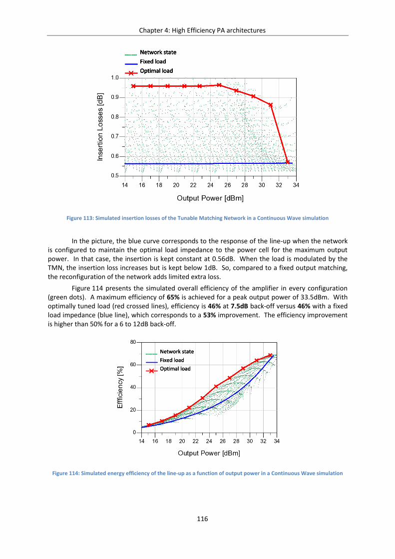
Chapter 4: High Efficiency PA architectures
116
Figure 113: Simulated insertion losses of the Tunable Matching Network in a Continuous Wave simulation
In the picture, the blue curve corresponds to the response of the line-up when the network is configured to maintain the optimal load impedance to the power cell for the maximum output power. In that case, the insertion is kept constant at 0.56dB. When the load is modulated by the TMN, the insertion loss increases but is kept below 1dB. So, compared to a fixed output matching, the reconfiguration of the network adds limited extra loss.
Figure 114 presents the simulated overall efficiency of the amplifier in every configuration (green dots). A maximum efficiency of 65% is achieved for a peak output power of 33.5dBm. With optimally tuned load (red crossed lines), efficiency is 46% at 7.5dB back-off versus 46% with a fixed load impedance (blue line), which corresponds to a 53% improvement. The efficiency improvement is higher than 50% for a 6 to 12dB back-off.
Figure 114: Simulated energy efficiency of the line-up as a function of output power in a Continuous Wave simulation
Network state
Fixed load
Optimal load
Network state
Fixed load
Optimal load
Network stateNetwork state
Fixed loadFixed load
Optimal loadOptimal load
Network state
Fixed load
Optimal load
Network state
Fixed load
Optimal load
Network stateNetwork state
Fixed loadFixed load
Optimal loadOptimal load
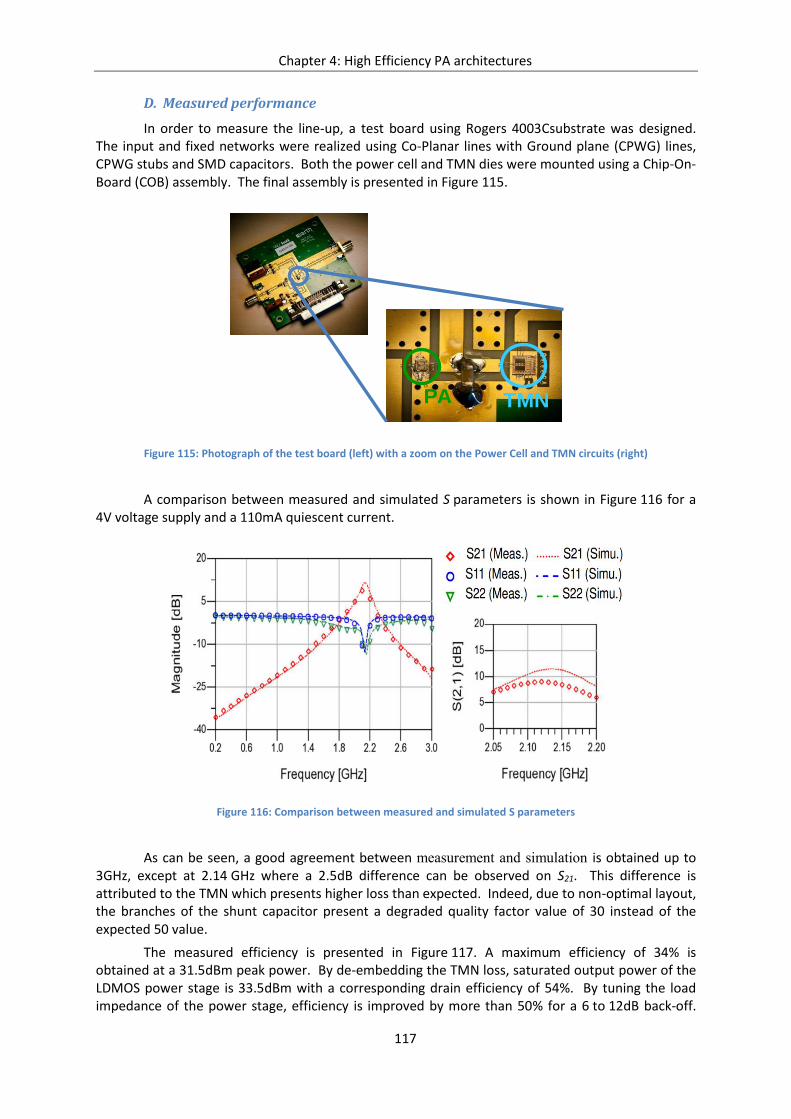
Chapter 4: High Efficiency PA architectures
117
D. Measured performance
In order to measure the line-up, a test board using Rogers 4003Csubstrate was designed. The input and fixed networks were realized using Co-Planar lines with Ground plane (CPWG) lines, CPWG stubs and SMD capacitors. Both the power cell and TMN dies were mounted using a Chip-On-Board (COB) assembly. The final assembly is presented in Figure 115.
Figure 115: Photograph of the test board (left) with a zoom on the Power Cell and TMN circuits (right)
A comparison between measured and simulated S parameters is shown in Figure 116 for a 4V voltage supply and a 110mA quiescent current.
Figure 116: Comparison between measured and simulated S parameters
As can be seen, a good agreement between measurement and simulation is obtained up to 3GHz, except at 2.14 GHz where a 2.5dB difference can be observed on S21. This difference is attributed to the TMN which presents higher loss than expected. Indeed, due to non-optimal layout, the branches of the shunt capacitor present a degraded quality factor value of 30 instead of the expected 50 value.
The measured efficiency is presented in Figure 117. A maximum efficiency of 34% is obtained at a 31.5dBm peak power. By de-embedding the TMN loss, saturated output power of the LDMOS power stage is 33.5dBm with a corresponding drain efficiency of 54%. By tuning the load impedance of the power stage, efficiency is improved by more than 50% for a 6 to 12dB back-off.
PA TMN
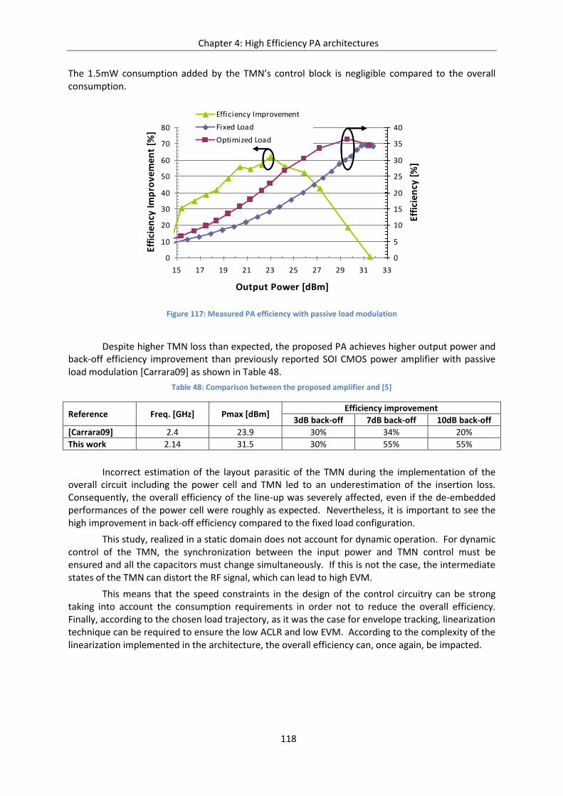
Chapter 4: High Efficiency PA architectures
118
The 1.5mW consumption added by the TMN’s control block is negligible compared to the overall consumption.
Figure 117: Measured PA efficiency with passive load modulation
Despite higher TMN loss than expected, the proposed PA achieves higher output power and back-off efficiency improvement than previously reported SOI CMOS power amplifier with passive load modulation [Carrara09] as shown in Table 48.
Table 48: Comparison between the proposed amplifier and [5]
Reference Freq. [GHz] Pmax [dBm] Efficiency improvement
3dB back-off 7dB back-off 10dB back-off
[Carrara09] 2.4 23.9 30% 34% 20%
This work 2.14 31.5 30% 55% 55%
Incorrect estimation of the layout parasitic of the TMN during the implementation of the overall circuit including the power cell and TMN led to an underestimation of the insertion loss. Consequently, the overall efficiency of the line-up was severely affected, even if the de-embedded performances of the power cell were roughly as expected. Nevertheless, it is important to see the high improvement in back-off efficiency compared to the fixed load configuration.
This study, realized in a static domain does not account for dynamic operation. For dynamic control of the TMN, the synchronization between the input power and TMN control must be ensured and all the capacitors must change simultaneously. If this is not the case, the intermediate states of the TMN can distort the RF signal, which can lead to high EVM.
This means that the speed constraints in the design of the control circuitry can be strong taking into account the consumption requirements in order not to reduce the overall efficiency. Finally, according to the chosen load trajectory, as it was the case for envelope tracking, linearization technique can be required to ensure the low ACLR and low EVM. According to the complexity of the linearization implemented in the architecture, the overall efficiency can, once again, be impacted.
0
10
20
30
40
50
60
70
80
15 17 19 21 23 25 27 29 31 33
Output Power [dBm]
Effi
cien
cy Im
pro
vem
ent
[%]
0
5
10
15
20
25
30
35
40
Effi
cien
cy [
%]
Efficiency Improvement
Fixed Load
Optimized Load
0
10
20
30
40
50
60
70
80
15 17 19 21 23 25 27 29 31 33
Output Power [dBm]
Effi
cien
cy Im
pro
vem
ent
[%]
0
5
10
15
20
25
30
35
40
Effi
cien
cy [
%]
Efficiency Improvement
Fixed Load
Optimized Load

Chapter 4: High Efficiency PA architectures
119
IV-5 Conclusion
In this chapter, PA efficiency enhancement has been studied. The efficiency decreases in traditional power amplifier at back-off. By varying either the supply voltage (envelope tracking technique: ET) or load impedance (load modulation technique: LM), the efficiency can be enhanced. However, both techniques apply to limited back-off ranges.
Concerning envelope tracking, the use of isogain envelope shaping is a way to improve efficiency without resorting to linearization. Simulation results show that this method is particularly efficient when amplifying complex signals such as W-CDMA release 99 and LTE. On the contrary, load modulation using isogain shaping degrades linearity. Therefore, in this case, a linearization technique is mandatory.
A load modulation power amplifier has been designed to assess the feasibility of this technique using the chosen SOI CMOS 130nm technology. After defining the load trajectory, a tunable network topology is chosen in order to adjust the load impedance of the power cell. The tunable capacitors of the tunable network were implemented as binary weighted switched capacitor banks. A prototype was realized and showed promising efficiency enhancement, higher than 50% for back-offs comprised between 6 to 12dB, with a 31.5dBm maximum output power despite higher loss in the tunable network than expected.
As a perspective, the study on high efficiency power amplifiers can be pursued by the study of architecture combining both ET and LM. Before transmission, according to the required average output power, the load of the power amplifier can be actuated thanks to a tunable matching network (static actuation). During the transmission, in order to handle the varying envelope, a supply modulator with isogain envelope shaping can ensure linear amplification of the signal with high efficiency.

Chapter 4: High Efficiency PA architectures
120
IV-6 References
[Carrara09] F. Carrara, C. D. Presti, F. Pappalardo, G. Palmisano, “A 2.4-GHz 24-dBm SOI CMOS Power Amplifier With Fully Integrated Reconfigurable Output Matching Network”, IEEE Transactions on Microwave Theory and Techniques, Vol. 57, No. 9, pp. 2122-2130, September 2009.
[Cripps06] S.-C. Cripps, “RF Power Amplifier for Wireless Applications – 2nd edition”, Artech House, 2006.
[Fager09] C. Fager, H.-M. Nemati, U. Gustavsson, R. Jos, H. Zirath, “Evaluation of High Efficiency PAs for use in Supply- and Load-Modulation Transmitters”, IEEE Power Amplifier Symposium presentation, 2009.
[Im13] D. Im and K. Lee, “Highly Linear Silicon on Insulator CMOS Digitally Programmable Capacitor Array for Tunable Antenna Matching Circuits”, IEEE Microwave and Wireless Components Letters, vol. 23, pp. 665-667, December 2013
[Nemati10] H. M. Nemati, A. L. Clarke, S. C. Cripps, J. Benedikt, P. J. Tasker, C. Fager, J. Grahn, H. Zirath, “Evaluation of a GaN HEMT Transistor for Load- and Supply-Modulation Applications Using Intrinsic Waveform Measurements”, IEEE Microwave Theory and Technique Symposium Digest, pp. 509-512, May 2010,
[Nujira12] G. Wimpeny, “Envelope Tracking (ET) PA Characterisation”, Nujira White Paper, February 24th 2012, retrieved from http://www.nujira.com/images/files/ET_PA_Characterisation_Dec%2014.pdf
[Popovic14] Z. Popovic, “Design and measurements of high-efficiency PAs with high PAR signals”, IEEE Automatic RF Techniques Group Workshop presentation, December 2014.
[Ranta13] T. Ranta, R. Whatley, C.-C. Cheng and M. Facchini, “Next-Generation CMOS on Insulator Multi-element Network For Broadband Antenna Tuning”, Proceedings of the European Microwave Conference, pp. 1567-1570, October 2013.
[Rijs06] F. van Rijs, S. J. C. H. Theeuwen, “Efficiency Improvement of LDMOS transistor for base stations: towards the theoretical limit”, in Electron Device Meeting, IEDM, Int., Dec 2006, pp. 1-4.
[SKY78010] Skyworks Inc., “SKY78010 Multiband Multimode Front-End Module for Quad-Band GSM / GPRS / EDGE – Penta-Band (Bands I, II, IV, V, VIII) WCDMA / HSPA / HSPA+ / LTE”, Product Datasheet, retrieved from http://www.skyworksinc.com/uploads/documents/SKY78010_202716A.pdf
[TQM756017] Triquint Semiconductors, “Multi-Mode (WCDMA B4, CDMA BC15, HSPA+, LTE) 3x3 PA Module”, Product Datasheet, retrieved from http://www.triquint.com/products/d/DOC-B-00000115
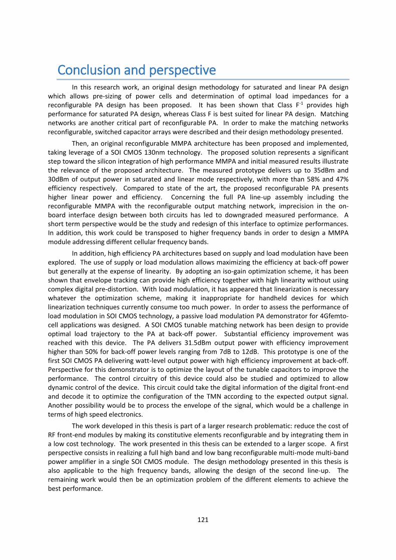
121
Conclusion and perspective In this research work, an original design methodology for saturated and linear PA design
which allows pre-sizing of power cells and determination of optimal load impedances for a reconfigurable PA design has been proposed. It has been shown that Class F-1 provides high performance for saturated PA design, whereas Class F is best suited for linear PA design. Matching networks are another critical part of reconfigurable PA. In order to make the matching networks reconfigurable, switched capacitor arrays were described and their design methodology presented.
Then, an original reconfigurable MMPA architecture has been proposed and implemented, taking leverage of a SOI CMOS 130nm technology. The proposed solution represents a significant step toward the silicon integration of high performance MMPA and initial measured results illustrate the relevance of the proposed architecture. The measured prototype delivers up to 35dBm and 30dBm of output power in saturated and linear mode respectively, with more than 58% and 47% efficiency respectively. Compared to state of the art, the proposed reconfigurable PA presents higher linear power and efficiency. Concerning the full PA line-up assembly including the reconfigurable MMPA with the reconfigurable output matching network, imprecision in the on-board interface design between both circuits has led to downgraded measured performance. A short term perspective would be the study and redesign of this interface to optimize performances. In addition, this work could be transposed to higher frequency bands in order to design a MMPA module addressing different cellular frequency bands.
In addition, high efficiency PA architectures based on supply and load modulation have been explored. The use of supply or load modulation allows maximizing the efficiency at back-off power but generally at the expense of linearity. By adopting an iso-gain optimization scheme, it has been shown that envelope tracking can provide high efficiency together with high linearity without using complex digital pre-distortion. With load modulation, it has appeared that linearization is necessary whatever the optimization scheme, making it inappropriate for handheld devices for which linearization techniques currently consume too much power. In order to assess the performance of load modulation in SOI CMOS technology, a passive load modulation PA demonstrator for 4Gfemto-cell applications was designed. A SOI CMOS tunable matching network has been design to provide optimal load trajectory to the PA at back-off power. Substantial efficiency improvement was reached with this device. The PA delivers 31.5dBm output power with efficiency improvement higher than 50% for back-off power levels ranging from 7dB to 12dB. This prototype is one of the first SOI CMOS PA delivering watt-level output power with high efficiency improvement at back-off. Perspective for this demonstrator is to optimize the layout of the tunable capacitors to improve the performance. The control circuitry of this device could also be studied and optimized to allow dynamic control of the device. This circuit could take the digital information of the digital front-end and decode it to optimize the configuration of the TMN according to the expected output signal. Another possibility would be to process the envelope of the signal, which would be a challenge in terms of high speed electronics.
The work developed in this thesis is part of a larger research problematic: reduce the cost of RF front-end modules by making its constitutive elements reconfigurable and by integrating them in a low cost technology. The work presented in this thesis can be extended to a larger scope. A first perspective consists in realizing a full high band and low bang reconfigurable multi-mode multi-band power amplifier in a single SOI CMOS module. The design methodology presented in this thesis is also applicable to the high frequency bands, allowing the design of the second line-up. The remaining work would then be an optimization problem of the different elements to achieve the best performance.

Conclusion
122
The high efficiency techniques should also be added to the full architecture to ensure high efficiency at power back-off. This can be done by adding a three state matching network at the output of both line-up and a high efficiency DC/DC converter. The three states matching network would allow pre-selection of the power level before transmission. The DC/DC converter would be used to implement an iso-gain envelope tracking technique to improve dynamically the efficiency of the device.
Towards a wider interest, the study on reconfiguration could be conducted on the full RF front-end by including the antenna, antenna tuner and switches. A system study with all these elements could reveal combinations of reconfigurable elements that lead to tremendous performance improvements. A co-design strategy would then be mandatory to efficiently exploit this study and create a fully reconfigurable front-end module. As SOI CMOS technology has a lot of potential for the integration of reconfigurable elements, it is logical that the use of this technology can be expanded on the full front-end module. The work presented in this thesis was the first steps towards the full implementation of SOI CMOS reconfigurable cellular RF front-end modules.
123
Published work
International conferences
[1] G. TANT, A. GIRY, P. FERRIS, G. PARES, J.-D. ARNOULD, J.-M. FOURNIER, C. RAYNAUD, P.VINCENT, « A SOI CMOS Reconfigurable Output Matching Network for Multimode Multiband Power Amplifiers », IEEE International Microwave Symposium, 2015.
[2] G. TANT, A. GIRY, J.-D. ARNOULD, J.-M. FOURNIER, P.VINCENT, « A 2.14GHz Watt-level Power Amplifier with Passive Load Modulation in a SOI CMOS technology », IEEE European Solid State Circuits Conference, pp. 189-192, 2013.
[4] A. GIRY, G. TANT, Y. LAMY, C. RAYNAUD, P.VINCENT, G. BERTRAND, S. JOBLOT, R.VELARD, P COUDRAIN, J.-F. CARPENTIER, D. PETIT, B. RAUDER, « A Monolithic Watt-level SOI LDMOS Linear Power Amplifier with Through Silicon Via for 4G Cellular Applications », IEEE Power Amplifier for Wireless and Radio Application Conference, pp. 19-21, 2013
National conferences
[4] G. TANT, P. FERRIS, A. GIRY, J.-D. ARNOULD, J.-M. FOURNIER, P.VINCENT, « Un réseau d’adaptation reconfigurable en technologie CMOS SOI pour amplificateur de puissance multimode multibandes », Journées Nationales Microondes, Bordeaux, 2015.
[5] P. FERRIS, G. TANT, D. PARAT, A. GIRY, J.-D. ARNOULD, J.-M. FOURNIER, « Un amplificateur de Puissance Multimode Multibande reconfigurable en technologie CMOS SOI », Journées Nationales Microondes, Bordeaux, 2015.
[6] G. TANT, A. GIRY, J.-D. ARNOULD, J.-M. FOURNIER, P.VINCENT, « Amplificateur de puissance à réseau de charge accordable en technologie SOI CMOS pour station de base Femtocell 4G », Journées Nationales Microondes, Paris, 2013.

Published work
124

125
Appendices
Appendix A: Fourier Coefficient Calculations
Useful integrals
The six integrals calculated hereafter will be useful for calculating Fourier coefficients.
∎ 𝐼1 = ∫ cos²(𝜃) 𝑑𝜃𝛼
0
= ∫1 + cos(2𝜃)
2𝑑𝜃
𝛼
0
=1
2(∫ 𝑑𝜃
𝛼
0
+∫ cos(2𝜃) 𝑑𝜃𝛼
0
)
𝐼1 =1
2(𝛼 +
sin(2𝛼)
2)
∎ 𝐼2 = ∫ cos²(2𝜃) 𝑑𝜃𝛼
0
= ∫1 + cos(4𝜃)
2𝑑𝜃
𝛼
0
=1
2(∫ 𝑑𝜃
𝛼
0
+∫ cos(4𝜃) 𝑑𝜃𝛼
0
)
𝐼2 =1
2(𝛼 +
sin(4𝛼)
4)
∎ For 𝑛 ≠ 1, 𝐼3(𝑛) = ∫ cos(𝜃) cos(𝑛𝜃) 𝑑𝜃𝛼
0
= ∫cos([𝑛 − 1]𝜃) + cos([𝑛 + 1]𝜃)
2𝑑𝜃
𝛼
0
=1
2(∫ cos([𝑛 − 1]𝜃) 𝑑𝜃
𝛼
0
+∫ cos([𝑛 + 1]𝜃) 𝑑𝜃𝛼
0
)
𝐼3(𝑛) =1
2(sin([𝑛 − 1]𝛼)
𝑛 − 1+sin([𝑛 + 1]𝛼)
𝑛 + 1) with 𝑛 ≠ 1
∎ For 𝑛 ≠ 2, 𝐼4(𝑛) = ∫ cos(2𝜃) cos(𝑛𝜃) 𝑑𝜃𝛼
0
= ∫cos([𝑛 − 2]𝜃) + cos([𝑛 + 2]𝜃)
2𝑑𝜃
𝛼
0
=1
2(∫ cos([𝑛 − 2]𝜃) 𝑑𝜃
𝛼
0
+∫ cos([𝑛 + 2]𝜃) 𝑑𝜃𝛼
0
)
𝐼4(𝑛) =1
2(sin([𝑛 − 2]𝛼)
𝑛 − 2+sin([𝑛 + 2]𝛼)
𝑛 + 2) with 𝑛 ≠ 2
Appendices
126
∎ For 𝑛 ≠ 2, 𝐼5(𝑛) = ∫ cos²(𝜃) cos(𝑛𝜃) 𝑑𝜃𝛼
0
= ∫1 + cos(2𝜃)
2cos(𝑛𝜃) 𝑑𝜃
𝛼
0
=1
2(∫ cos(𝑛𝜃) 𝑑𝜃
𝛼
0
+∫ cos(2𝜃) cos(𝑛𝜃) 𝑑𝜃𝛼
0
) =1
2(sin(𝑛𝛼)
𝑛+ 𝐼4(𝑛))
𝐼5(𝑛) =1
2(sin(𝑛𝛼)
𝑛+1
2(sin([𝑛 − 2]𝛼)
𝑛 − 2+sin([𝑛 + 2]𝛼)
𝑛 + 2)) with 𝑛 ≠ 2
∎ 𝐼5(1) = ∫ 𝑐𝑜𝑠²(𝜃) 𝑐𝑜𝑠(𝜃) 𝑑𝜃𝛼
0
=1
2(𝑠𝑖𝑛(𝛼) +
1
2(𝑠𝑖𝑛(3𝜃)
3− 𝑠𝑖𝑛(−𝛼))) =
1
2(3
2𝑠𝑖𝑛(𝛼) +
1
2(𝑠𝑖𝑛(3𝛼)
3))
𝐼5(1) =1
4(3 sin(𝛼) +
sin(3𝛼)
3)
∎ 𝐼6 = ∫ cos²(𝜃) cos(2𝜃) 𝑑𝜃𝛼
0
= ∫1 + cos(2𝜃)
2cos(2𝜃) 𝑑𝜃
𝛼
0
=1
2(∫ cos(2𝜃) 𝑑𝜃
𝛼
0
+∫ cos²(2𝜃) 𝑑𝜃𝛼
0
)
=1
2(sin(2𝛼)
2+ 𝐼2) =
1
2(sin(2𝛼)
2+1
2(𝛼 +
sin(4𝛼)
4))
𝐼6 =1
4(𝛼 + sin(2𝛼) +
sin(4𝛼)
4)
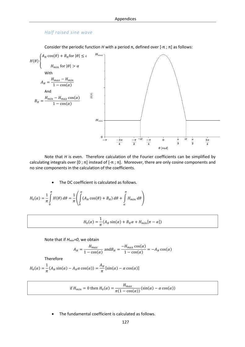
Appendices
127
Half raised sine wave
Consider the periodic function H with a period π, defined over [-π ; π] as follows:
𝐻(𝜃)
𝐴𝐻 cos(𝜃) + 𝐵𝐻for |𝜃| ≤ 𝛼
𝐻𝑚𝑖𝑛 for |𝜃| > 𝛼
With
𝐴𝐻 =𝐻𝑚𝑎𝑥 −𝐻𝑚𝑖𝑛1 − cos(𝛼)
And
𝐵𝐻 =𝐻𝑚𝑖𝑛 − 𝐻𝑚𝑎𝑥 cos(𝛼)
1 − cos(𝛼)
Note that H is even. Therefore calculation of the Fourier coefficients can be simplified by calculating integrals over [0 ; π] instead of [-π ; π]. Moreover, there are only cosine components and no sine components in the calculation of the coefficients.
The DC coefficient is calculated as follows.
𝐻0(𝛼) =1
𝜋∫𝐻(𝜃) 𝑑𝜃
𝜋
0
=1
𝜋(∫(𝐴𝐻 cos(𝜃) + 𝐵𝐻) 𝑑𝜃
𝛼
0
+ ∫𝐻𝑚𝑖𝑛 𝑑𝜃
𝜋
𝛼
)
𝐻0(𝛼) =1
𝜋(𝐴𝐻 sin(𝛼) + 𝐵𝐻𝛼 + 𝐻𝑚𝑖𝑛[𝜋 − 𝛼])
Note that if Hmin=0, we obtain
𝐴𝐻 =𝐻𝑚𝑎𝑥
1 − cos(𝛼) and𝐵𝐻 =
−𝐻𝑚𝑎𝑥 cos(𝛼)
1 − cos(𝛼)= −𝐴𝐻 cos(𝛼)
Therefore
𝐻0(𝛼) =1
𝜋(𝐴𝐻 sin(𝛼) − 𝐴𝐻𝛼 cos(𝛼)) =
𝐴𝐻𝜋[sin(𝛼) − 𝛼 cos(𝛼)]
if 𝐻𝑚𝑖𝑛 = 0 then 𝐻0(𝛼) =𝐻𝑚𝑎𝑥
𝜋(1 − cos(𝛼))(sin(𝛼) − 𝛼 cos(𝛼))
The fundamental coefficient is calculated as follows.
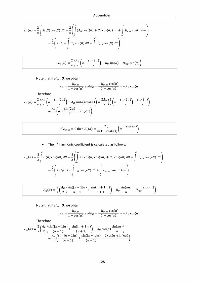
Appendices
128
𝐻1(𝛼) =2
𝜋∫𝐻(𝜃) cos(𝜃) 𝑑𝜃
𝜋
0
=2
𝜋(∫(𝐴𝐻 cos²(𝜃) + 𝐵𝐻 cos(𝜃)) 𝑑𝜃
𝛼
0
+ ∫𝐻𝑚𝑖𝑛 cos(𝜃) 𝑑𝜃
𝜋
𝛼
)
=2
𝜋(𝐴𝐻𝐼1 +∫𝐵𝐻 cos(𝜃) 𝑑𝜃
𝛼
0
+ ∫𝐻𝑚𝑖𝑛 cos(𝜃) 𝑑𝜃
𝜋
𝛼
)
𝐻1(𝛼) =2
𝜋(𝐴𝐻2(𝛼 +
sin(2𝛼)
2) + 𝐵𝐻 sin(𝛼) − 𝐻𝑚𝑖𝑛 sin(𝛼))
Note that if Hmin=0, we obtain
𝐴𝐻 =𝐻𝑚𝑎𝑥
1 − cos(𝛼) and𝐵𝐻 =
−𝐻𝑚𝑎𝑥 cos(𝛼)
1 − cos(𝛼)= −𝐴𝐻 cos(𝛼)
Therefore
𝐻1(𝛼) =2
𝜋(𝐴𝐻2(𝛼 +
sin(2𝛼)
2) − 𝐴𝐻 sin(𝛼) cos(𝛼)) =
2𝐴𝐻𝜋
(1
2(𝛼 +
sin(2𝛼)
2) −
sin(2𝛼)
2)
=𝐴𝐻𝜋(𝛼 +
sin(2𝛼)
2− sin(2𝛼))
if 𝐻𝑚𝑖𝑛 = 0 then 𝐻1(𝛼) =𝐻𝑚𝑎𝑥
𝜋(1 − cos(𝛼))(𝛼 −
sin(2𝛼)
2)
The nth harmonic coefficient is calculated as follows.
𝐻𝑛(𝛼) =2
𝜋∫𝐻(𝜃) cos(𝑛𝜃) 𝑑𝜃
𝜋
0
=2
𝜋(∫𝐴𝐻 cos(𝜃) cos(𝑛𝜃) + 𝐵𝐻 cos(𝑛𝜃) 𝑑𝜃
𝛼
0
+ ∫𝐻𝑚𝑖𝑛 cos(𝑛𝜃) 𝑑𝜃
𝜋
𝛼
)
=2
𝜋(𝐴𝐻𝐼3(𝑛) + ∫𝐵𝐻 cos(𝑛𝜃) 𝑑𝜃
𝛼
0
+ ∫𝐻𝑚𝑖𝑛 cos(𝑛𝜃) 𝑑𝜃
𝜋
𝛼
)
𝐻𝑛(𝛼) =2
𝜋(𝐴𝐻2(sin([𝑛 − 1]𝛼)
𝑛 − 1+sin([𝑛 + 1]𝛼)
𝑛 + 1) + 𝐵𝐻
sin(𝑛𝛼)
𝑛− 𝐻𝑚𝑖𝑛
sin(𝑛𝛼)
𝑛)
Note that if Hmin=0, we obtain
𝐴𝐻 =𝐻𝑚𝑎𝑥
1 − cos(𝛼) and𝐵𝐻 =
−𝐻𝑚𝑎𝑥 cos(𝛼)
1 − cos(𝛼)= −𝐴𝐻 cos(𝛼)
Therefore
𝐻𝑛(𝛼) =2
𝜋(𝐴𝐻2(sin([𝑛 − 1]𝛼)
(𝑛 − 1)+sin([𝑛 + 1]𝛼)
(𝑛 + 1)) − 𝐴𝐻 cos(𝛼)
sin(𝑛𝛼)
𝑛)
=𝐴𝐻𝜋(sin([𝑛 − 1]𝛼)
(𝑛 − 1)+sin([𝑛 + 1]𝛼)
(𝑛 + 1)−2 cos(𝛼) sin(𝑛𝛼)
𝑛)

Appendices
129
if 𝐻𝑚𝑖𝑛 = 0 then 𝐻𝑛(𝛼) =𝐻𝑚𝑎𝑥
𝜋(1 − cos(𝛼))(sin([𝑛 − 1]𝛼)
(𝑛 − 1)+sin([𝑛 + 1]𝛼)
(𝑛 + 1)−2 cos(𝛼) sin(𝑛𝛼)
𝑛)

Appendices
130
Half squared sine wave
Consider the periodic function Q with a period π, defined over [-π ; π] as follows:
𝑄(𝜃) (𝐴𝑄 cos(𝜃) + 𝐵𝑄)
2for |𝜃| ≤ 𝛼
𝑄𝑚𝑖𝑛 for |𝜃| > 𝛼
With
𝐴𝑄 =√𝑄𝑚𝑎𝑥 − √𝑄𝑚𝑖𝑛1 − cos(𝛼)
And
𝐵𝑄 =√𝑄𝑚𝑖𝑛 − √𝑄𝑚𝑎𝑥 cos(𝛼)
1 − cos(𝛼)
Note that Q is even. Therefore calculation of the Fourier coefficients can be simplified by calculating integrals over [0 ; π] instead of [-π ; π]. Moreover, there are only cosine components and no sine components in the calculation of the coefficients.
The DC coefficient is calculated as follows.
𝑄0(𝛼) =1
𝜋∫𝑄(𝜃) 𝑑𝜃
𝜋
0
=1
𝜋(∫𝐴𝑄
2 cos²(𝜃) + 2𝐴𝑄𝐵𝑄 cos(𝜃) + 𝐵𝑄2 𝑑𝜃
𝛼
0
+ ∫𝑄𝑚𝑖𝑛 𝑑𝜃
𝜋
𝛼
)
=1
𝜋(𝐴𝑄
2 𝐼1 +∫2𝐴𝑄𝐵𝑄 cos(𝜃) 𝑑𝜃
𝛼
0
+∫𝐵𝑄2 𝑑𝜃
𝛼
0
+ ∫𝑄𝑚𝑖𝑛 𝑑𝜃
𝜋
𝛼
)
𝑄0(𝛼) =1
𝜋(𝐴𝑄2
2(𝛼 +
sin(2𝛼)
2) + 2𝐴𝑄𝐵𝑄 sin(𝛼) + 𝐵𝑄
2𝛼 + 𝑄𝑚𝑖𝑛[𝜋 − 𝛼])
Note that if Qmin=0, we obtain
𝐴𝑄 =√𝑄𝑚𝑎𝑥
1 − cos(𝛼) and𝐵𝑄 =
−√𝑄𝑚𝑎𝑥 cos(𝛼)
1 − cos(𝛼)= −𝐴𝑄 cos(𝛼)
Therefore
𝑄0(𝛼) =1
𝜋(𝐴𝑄2
2(𝛼 +
sin(2𝛼)
2) − 2𝐴𝑄
2 cos(𝛼) sin(𝛼) + 𝐴𝑄2 cos²(𝛼) 𝛼)
=𝐴𝑄2
𝜋(𝛼
2+sin(2𝛼)
4− sin(2𝛼) + 𝛼
1 + cos(2𝛼)
2) =
𝐴𝑄2
2(𝛼
2+𝛼
2−3 sin(2𝛼)
4+ 𝛼 cos(2𝛼))
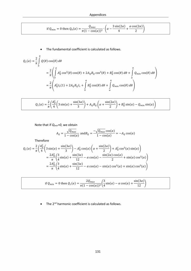
Appendices
131
if 𝑄𝑚𝑖𝑛 = 0 then 𝑄0(𝛼) =𝑄𝑚𝑎𝑥
𝜋(1 − cos(𝛼))2∙ (𝛼 −
3 sin(2𝛼)
4+𝛼 cos(2𝛼)
2)
The fundamental coefficient is calculated as follows.
𝑄1(𝛼) =2
𝜋∫𝑄(𝜃) cos(𝜃) 𝑑𝜃
𝜋
0
=2
𝜋(∫𝐴𝑄
2 cos²(𝜃) cos(𝜃) + 2𝐴𝑄𝐵𝑄 cos²(𝜃) + 𝐵𝑄2 cos(𝜃) 𝑑𝜃
𝛼
0
+ ∫𝑄𝑚𝑖𝑛 cos(𝜃) 𝑑𝜃
𝜋
𝛼
)
=2
𝜋(𝐴𝑄
2 𝐼5(1) + 2𝐴𝑄𝐵𝑄𝐼1 +∫𝐵𝑄2 cos(𝜃) 𝑑𝜃
𝛼
0
+ ∫𝑄𝑚𝑖𝑛 cos(𝜃) 𝑑𝜃
𝜋
𝛼
)
𝑄1(𝛼) =2
𝜋(𝐴𝑄2
4(3 sin(𝛼) +
sin(3𝛼)
3) + 𝐴𝑄𝐵𝑄 (𝛼 +
sin(2𝛼)
2) + 𝐵𝑄
2 sin(𝛼) − 𝑄𝑚𝑖𝑛 sin(𝛼))
Note that if Qmin=0, we obtain
𝐴𝑄 =√𝑄𝑚𝑎𝑥
1 − cos(𝛼) and𝐵𝑄 =
−√𝑄𝑚𝑎𝑥 cos(𝛼)
1 − cos(𝛼)= −𝐴𝑄 cos(𝛼)
Therefore
𝑄1(𝛼) =2
𝜋(𝐴𝑄2
4(3 sin(𝛼) +
sin(3𝛼)
3) − 𝐴𝑄
2 cos(𝛼) (𝛼 +sin(2𝛼)
2) + 𝐴𝑄
2 cos²(𝛼) sin(𝛼))
=2𝐴𝑄
2
𝜋(3
4sin(𝛼) +
sin(3𝛼)
12− 𝛼 cos(𝛼) −
sin(2𝛼) cos(𝛼)
2+ sin(𝛼) cos²(𝛼))
=2𝐴𝑄
2
𝜋(3
4sin(𝛼) +
sin(3𝛼)
12− 𝛼 cos(𝛼) − sin(𝛼) cos²(𝛼) + sin(𝛼) cos²(𝛼))
if 𝑄𝑚𝑖𝑛 = 0 then 𝑄1(𝛼) =2𝑄𝑚𝑎𝑥
𝜋(1 − cos(𝛼))2(3
4sin(𝛼) − 𝛼 cos(𝛼) +
sin(3𝛼)
12)
The 2nd harmonic coefficient is calculated as follows.
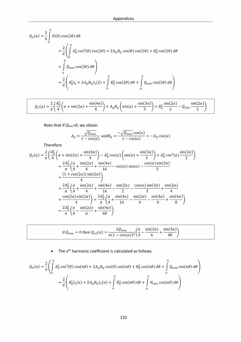
Appendices
132
𝑄2(𝛼) =2
𝜋∫𝐻(𝜃) cos(2𝜃) 𝑑𝜃
𝜋
0
=2
𝜋(∫𝐴𝑄
2 cos²(𝜃) cos(2𝜃) + 2𝐴𝑄𝐵𝑄 cos(𝜃) cos(2𝜃) + 𝐵𝑄2 cos(2𝜃) 𝑑𝜃
𝛼
0
+ ∫𝑄𝑚𝑖𝑛 cos(2𝜃) 𝑑𝜃
𝜋
𝛼
)
=2
𝜋(𝐴𝑄
2 𝐼6 + 2𝐴𝑄𝐵𝑄𝐼3(2) + ∫𝐵𝑄2 cos(2𝜃) 𝑑𝜃
𝛼
0
+ ∫𝑄𝑚𝑖𝑛 cos(2𝜃) 𝑑𝜃
𝜋
𝛼
)
𝑄2(𝛼) =2
𝜋(𝐴𝑄2
4(𝛼 + sin(2𝛼) +
sin(4𝛼)
4) + 𝐴𝑄𝐵𝑄 (sin(𝛼) +
sin(3𝛼)
3) + 𝐵𝑄
2sin(2𝛼)
2− 𝑄𝑚𝑖𝑛
sin(2𝛼)
2)
Note that if Qmin=0, we obtain
𝐴𝑄 =√𝑄𝑚𝑎𝑥
1 − cos(𝛼) and𝐵𝑄 =
−√𝑄𝑚𝑎𝑥 cos(𝛼)
1 − cos(𝛼)= −𝐴𝑄 cos(𝛼)
Therefore
𝑄2(𝛼) =2
𝜋(𝐴𝑄2
4(𝛼 + sin(2𝛼) +
sin(4𝛼)
4) − 𝐴𝑄
2 cos(𝛼) (sin(𝛼) +sin(3𝛼)
3) + 𝐴𝑄
2 cos²(𝛼)sin(2𝛼)
2)
=2𝐴𝑄
2
𝜋(𝛼
4+sin(2𝛼)
4+sin(4𝛼)
16− cos(𝛼) sin(𝛼) −
cos(𝛼) sin(3𝛼)
3
+(1 + cos(2𝛼)) sin(2𝛼)
4)
=2𝐴𝑄
2
𝜋(𝛼
4+sin(2𝛼)
4+sin(4𝛼)
16−sin(2𝛼)
2−cos(𝛼) sin(3𝛼)
3+sin(2𝛼)
4
+cos(2𝛼) sin(2𝛼)
4) =
2𝐴𝑄2
𝜋(𝛼
4+sin(4𝛼)
16−sin(2𝛼)
6−sin(4𝛼)
6+sin(4𝛼)
8)
=2𝐴𝑄
2
𝜋(𝛼
4−sin(2𝛼)
6+sin(4𝛼)
48)
if 𝑄𝑚𝑖𝑛 = 0 then 𝑄𝑛2(𝛼) =2𝑄𝑚𝑎𝑥
𝜋(1 − cos(𝛼))2(𝛼
4−sin(2𝛼)
6+sin(4𝛼)
48)
The nth harmonic coefficient is calculated as follows.
𝑄𝑛(𝛼) =2
𝜋(∫𝐴𝑄
2 cos²(𝜃) cos(𝑛𝜃) + 2𝐴𝑄𝐵𝑄 cos(𝜃) cos(𝑛𝜃) + 𝐵𝑄2 cos(𝑛𝜃) 𝑑𝜃
𝛼
0
+ ∫𝑄𝑚𝑖𝑛 cos(𝑛𝜃) 𝑑𝜃
𝜋
𝛼
)
=2
𝜋(𝐴𝑄
2 𝐼5(𝑛) + 2𝐴𝑄𝐵𝑄𝐼3(𝑛) + ∫ 𝐵𝑄2 cos(𝑛𝜃) 𝑑𝜃
𝛼
0
+ ∫𝐻𝑚𝑖𝑛 cos(𝑛𝜃) 𝑑𝜃
𝜋
𝛼
)

Appendices
133
𝑄𝑛(𝛼) =2
𝜋(𝐴𝑄2
2(sin(𝑛𝛼)
𝑛+1
2(sin([𝑛 − 2]𝛼)
𝑛 − 2+sin([𝑛 + 2]𝛼)
𝑛 + 2)) + 𝐴𝑄𝐵𝑄 (
sin([𝑛 − 1]𝛼)
𝑛 − 1+sin([𝑛 + 1]𝛼)
𝑛 + 1)
+ 𝐵𝑄2sin(𝑛𝛼)
𝑛− 𝐻𝑚𝑖𝑛
sin(𝑛𝛼)
𝑛)
Note that if Qmin=0, we obtain
𝐴𝑄 =√𝑄𝑚𝑎𝑥
1 − cos(𝛼) and𝐵𝑄 =
−√𝑄𝑚𝑎𝑥 cos(𝛼)
1 − cos(𝛼)= −𝐴𝑄 cos(𝛼)
Therefore
𝑄𝑛(𝛼) =2
𝜋(𝐴𝑄2
2(sin(𝑛𝛼)
𝑛+1
2(sin([𝑛 − 2]𝛼)
𝑛 − 2+sin([𝑛 + 2]𝛼)
𝑛 + 2))
− 𝐴𝑄2 cos(𝛼) (
sin([𝑛 − 1]𝛼)
𝑛 − 1+sin([𝑛 + 1]𝛼)
𝑛 + 1) + 𝐴𝑄
2 cos²(𝛼)sin(𝑛𝛼)
𝑛)
=2𝐴𝑄
2
𝜋(sin(𝑛𝛼)
2𝑛+1
4(sin([𝑛 − 2]𝛼)
𝑛 − 2+sin([𝑛 + 2]𝛼)
𝑛 + 2)
− cos(𝛼) (sin([𝑛 − 1]𝛼)
𝑛 − 1+sin([𝑛 + 1]𝛼)
𝑛 + 1) +
(1 + cos(2𝛼)) sin(𝑛𝛼)
2𝑛)
=2𝐴𝑄
2
𝜋(sin(𝑛𝛼)
𝑛+1
4(sin([𝑛 − 2]𝛼)
𝑛 − 2+sin([𝑛 + 2]𝛼)
𝑛 + 2)
− (sin([𝑛 − 1]𝛼) cos(𝛼)
𝑛 − 1+sin([𝑛 + 1]𝛼) cos(𝛼)
𝑛 + 1) +
sin(𝑛𝛼) cos(2𝛼)
2𝑛)
=2𝐴𝑄
2
𝜋(sin(𝑛𝛼)
𝑛+1
4(sin([𝑛 − 2]𝛼)
𝑛 − 2+sin([𝑛 + 2]𝛼)
𝑛 + 2)
− (sin(𝑛𝛼) + sin([𝑛 − 2]𝛼)
2(𝑛 − 1)+sin([𝑛 + 2]𝛼) + sin(𝑛𝛼)
2(𝑛 + 1))
+sin([𝑛 − 2]𝛼) + sin([𝑛 + 2]𝛼)
4𝑛)
=2𝐴𝑄
2
𝜋(sin(𝑛𝛼) [
1
𝑛−
1
2(𝑛 − 1)−
1
2(𝑛 + 1)] + sin([𝑛 − 2]𝛼) [
1
4𝑛−
1
2(𝑛 − 1)−
1
4(𝑛 − 2)]
+ sin([𝑛 + 2]𝛼) [1
4𝑛−
1
2(𝑛 + 1)−
1
4(𝑛 + 2)])
=2𝐴𝑄
2
𝜋(− sin(𝑛𝛼)
1
𝑛(𝑛2 − 1)+ sin([𝑛 − 2]𝛼)
1
2𝑛(𝑛 − 1)(𝑛 − 2)
+ sin([𝑛 + 2]𝛼)1
2𝑛(𝑛 + 1)(𝑛 + 2))
=2𝐴𝑄
2
𝜋((4 − 𝑛2) sin(𝑛𝛼) +
(𝑛+1)(𝑛+2) sin([𝑛−2]𝛼)
2+
(𝑛−1)(𝑛−2) sin([𝑛+2]𝛼)
2
𝑛(𝑛2 − 1)(𝑛2 − 4))
=2𝐴𝑄
2
𝜋((4 − 𝑛2) sin(𝑛𝛼) + +
(𝑛−1)(𝑛−2)(sin([𝑛+2]𝛼)+sin([𝑛−2]𝛼))
2+ 3𝑛 sin([𝑛 − 2]𝛼)
𝑛(𝑛2 − 1)(𝑛2 − 4))
if 𝑄𝑚𝑖𝑛 = 0 then
𝑄𝑛(𝛼) =𝐻𝑚𝑎𝑥
𝜋(1 − cos(𝛼))((4 − 𝑛2) sin(𝑛𝛼) + (𝑛 − 1)(𝑛 − 2) sin(𝑛𝛼) cos(𝜑) + 3𝑛 sin((𝑛 − 2)𝛼)
𝑛(𝑛2 − 1)(𝑛2 − 4))
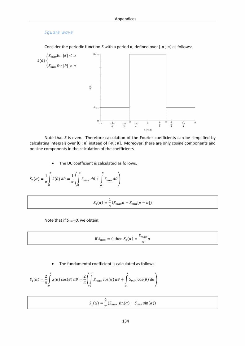
Appendices
134
Square wave
Consider the periodic function S with a period π, defined over [-π ; π] as follows:
𝑆(𝜃)
𝑆𝑚𝑎𝑥for |𝜃| ≤ 𝛼
𝑆𝑚𝑖𝑛 for |𝜃| > 𝛼
Note that S is even. Therefore calculation of the Fourier coefficients can be simplified by calculating integrals over [0 ; π] instead of [-π ; π]. Moreover, there are only cosine components and no sine components in the calculation of the coefficients.
The DC coefficient is calculated as follows.
𝑆0(𝛼) =1
𝜋∫ 𝑆(𝜃) 𝑑𝜃
𝜋
0
=1
𝜋(∫ 𝑆𝑚𝑎𝑥 𝑑𝜃
𝛼
0
+ ∫𝑆𝑚𝑖𝑛 𝑑𝜃
𝜋
𝛼
)
𝑆0(𝛼) =1
𝜋(𝑆𝑚𝑎𝑥𝛼 + 𝑆𝑚𝑖𝑛[𝜋 − 𝛼])
Note that if Smin=0, we obtain:
if 𝑆𝑚𝑖𝑛 = 0 then 𝑆0(𝛼) =𝑆𝑚𝑎𝑥𝜋
𝛼
The fundamental coefficient is calculated as follows.
𝑆1(𝛼) =2
𝜋∫ 𝑆(𝜃) cos(𝜃) 𝑑𝜃
𝜋
0
=2
𝜋(∫ 𝑆𝑚𝑎𝑥 cos(𝜃) 𝑑𝜃
𝛼
0
+ ∫𝑆𝑚𝑖𝑛 cos(𝜃) 𝑑𝜃
𝜋
𝛼
)
𝑆1(𝛼) =2
𝜋(𝑆𝑚𝑎𝑥 sin(𝛼) − 𝑆𝑚𝑖𝑛 sin(𝛼))
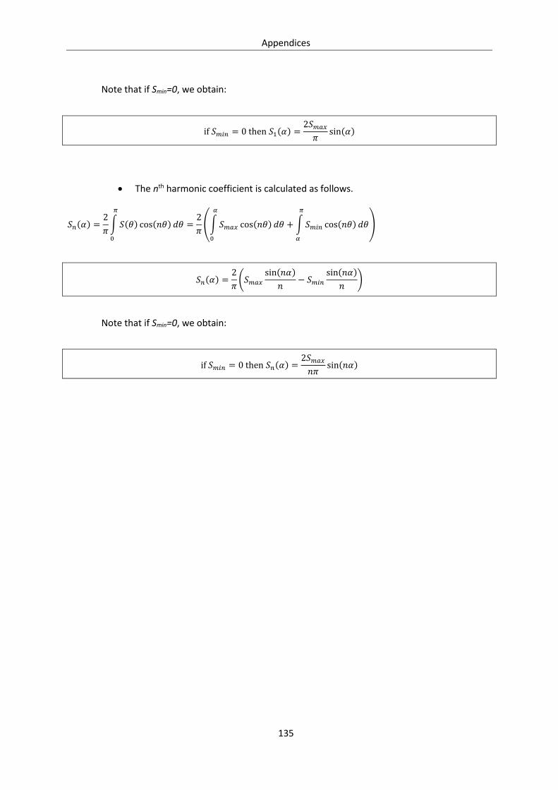
Appendices
135
Note that if Smin=0, we obtain:
if 𝑆𝑚𝑖𝑛 = 0 then 𝑆1(𝛼) =2𝑆𝑚𝑎𝑥𝜋
sin(𝛼)
The nth harmonic coefficient is calculated as follows.
𝑆𝑛(𝛼) =2
𝜋∫ 𝑆(𝜃) cos(𝑛𝜃) 𝑑𝜃
𝜋
0
=2
𝜋(∫ 𝑆𝑚𝑎𝑥 cos(𝑛𝜃) 𝑑𝜃
𝛼
0
+ ∫𝑆𝑚𝑖𝑛 cos(𝑛𝜃) 𝑑𝜃
𝜋
𝛼
)
𝑆𝑛(𝛼) =2
𝜋(𝑆𝑚𝑎𝑥
sin(𝑛𝛼)
𝑛− 𝑆𝑚𝑖𝑛
sin(𝑛𝛼)
𝑛)
Note that if Smin=0, we obtain:
if 𝑆𝑚𝑖𝑛 = 0 then 𝑆𝑛(𝛼) =2𝑆𝑚𝑎𝑥𝑛𝜋
sin(𝑛𝛼)

Appendices
136
Appendix B: Current and voltage coefficients calculation in non-
sinusoidal classes
Class F
In class F, the current wave form is defined by function 𝐻(𝜃) for 𝛼 = 𝜋 2⁄ and 𝐻𝑚𝑖𝑛 = 0.
Therefore
∎ 𝐼𝑑𝑠[0] = 𝐻0 (𝜋
2) =
𝐻𝑚𝑎𝑥𝜋
=𝐼𝑚𝑎𝑥𝜋
𝐼𝑑𝑠[0] =𝐼𝑚𝑎𝑥𝜋
∎ 𝐼𝑑𝑠[𝑓0] = 𝐻1 (𝜋
2) =
𝐻𝑚𝑎𝑥𝜋
∙𝜋
2=𝐼𝑚𝑎𝑥2
𝐼𝑑𝑠[𝑓0] =𝐼𝑚𝑎𝑥2
In class F, the voltage wave form is defined by function 𝑆(𝜃) for 𝛼 = 𝜋 2⁄ . Moreover, VDS[0] is forced to VDD by the supply and Smin=Vk due to the on-state resistance of the transistor.
Therefore
∎ 𝑉𝑑𝑠[0] = 𝑆0 (𝜋
2) =
1
𝜋(𝑆𝑚𝑎𝑥
𝜋
2+ 𝑆𝑚𝑖𝑛
𝜋
2) =
𝑆𝑚𝑎𝑥 + 𝑉𝑘2
= 𝑉𝐷𝐷
Therefore
𝑆𝑚𝑎𝑥 = 2𝑉𝐷𝐷 − 𝑉𝑘
∎ 𝑉𝑑𝑠[𝑓0] = 𝑆1 (𝜋
2) =
2
𝜋(𝑆𝑚𝑎𝑥 − 𝑆𝑚𝑖𝑛) =
2
𝜋(2𝑉𝐷𝐷 − 𝑉𝑘 − 𝑉𝑘) =
4
𝜋(𝑉𝐷𝐷 − 𝑉𝑘)
𝑉𝑑𝑠[𝑓0] =4
𝜋(𝑉𝐷𝐷 − 𝑉𝑘)

Appendices
137
Class F -1
In class F-1, the current wave form is defined by function 𝑆(𝜃) for 𝛼 = 𝜋 2⁄ and 𝑆𝑚𝑖𝑛 = 0.
Therefore
∎ 𝐼𝑑𝑠[0] = 𝑆0 (𝜋
2) =
1
𝜋∙ 𝑆𝑚𝑎𝑥
𝜋
2=𝐼𝑚𝑎𝑥2
𝐼𝑑𝑠[0] =𝐼𝑚𝑎𝑥2
∎ 𝐼𝑑𝑠[𝑓0] = 𝑆1 (𝜋
2) =
2𝑆𝑚𝑎𝑥𝜋
=2𝐼𝑚𝑎𝑥𝜋
𝐼𝑑𝑠[𝑓0] =2𝐼𝑚𝑎𝑥𝜋
In class F, the voltage wave form is defined by function 𝐻(𝜃) for 𝛼 = 𝜋 2⁄ . Moreover, VDS[0] is forced to VDD by the supply and Hmin=Vk due to the on-state resistance of the transistor.
Therefore
∎ 𝑉𝑑𝑠[0] = 𝐻0 (𝜋
2) =
1
𝜋(𝐴𝐻 + 𝐵𝐻
𝜋
2+ 𝐻𝑚𝑖𝑛
𝜋
2) =
1
𝜋(𝐻𝑚𝑎𝑥 − 𝐻𝑚𝑖𝑛 +𝐻𝑚𝑖𝑛
𝜋
2+ 𝐻𝑚𝑖𝑛
𝜋
2)
=𝐻𝑚𝑎𝑥𝜋
+(𝜋 − 1)
𝜋𝑉𝑘 = 𝑉𝐷𝐷
Therefore
𝐻𝑚𝑎𝑥 = 𝜋𝑉𝐷𝐷 − (𝜋 − 1)𝑉𝑘
Then
𝐴𝐻 = 𝜋𝑉𝐷𝐷 − (𝜋 − 1)𝑉𝑘 − 𝑉𝑘 = 𝜋𝑉𝐷𝐷 − 𝜋𝑉𝑘 + 𝑉𝑘 − 𝑉𝑘
𝐴𝐻 = 𝜋(𝑉𝐷𝐷 − 𝑉𝑘) and𝐵𝐻 = 𝑉𝑘
∎ 𝑉𝑑𝑠[𝑓0] = 𝐻1 (𝜋
2) =
2
𝜋(𝐴𝐻2∙𝜋
2+ 𝐵𝐻 − 𝐻𝑚𝑖𝑛) =
𝐴𝐻2+ 𝑉𝑘 − 𝑉𝑘 =
𝜋(𝑉𝐷𝐷 − 𝑉𝑘)
2
𝑉𝑑𝑠[𝑓0] =𝜋
2(𝑉𝐷𝐷 − 𝑉𝑘)
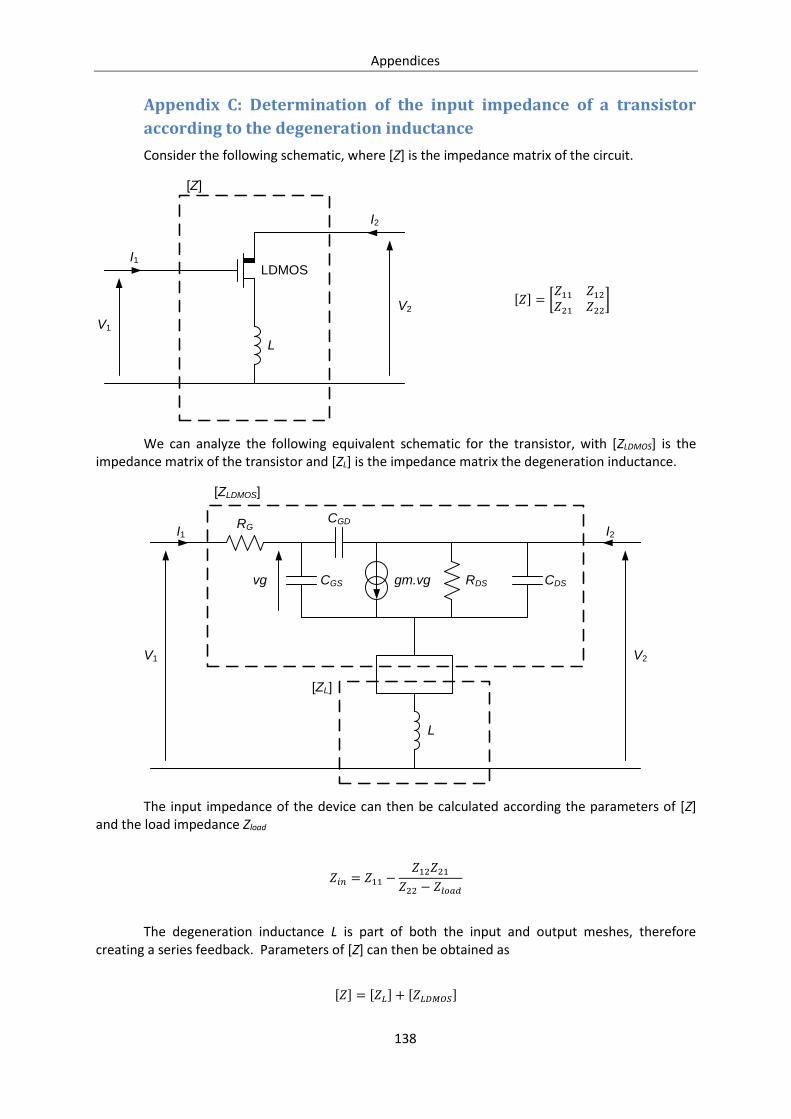
Appendices
138
Appendix C: Determination of the input impedance of a transistor
according to the degeneration inductance
Consider the following schematic, where [Z] is the impedance matrix of the circuit.
[𝑍] = [𝑍11 𝑍12𝑍21 𝑍22
]
We can analyze the following equivalent schematic for the transistor, with [ZLDMOS] is the impedance matrix of the transistor and [ZL] is the impedance matrix the degeneration inductance.
The input impedance of the device can then be calculated according the parameters of [Z] and the load impedance Zload
𝑍𝑖𝑛 = 𝑍11 −𝑍12𝑍21
𝑍22 − 𝑍𝑙𝑜𝑎𝑑
The degeneration inductance L is part of both the input and output meshes, therefore creating a series feedback. Parameters of [Z] can then be obtained as
[𝑍] = [𝑍𝐿] + [𝑍𝐿𝐷𝑀𝑂𝑆]
I1
I2
V1
V2
[Z]
L
LDMOS
I1 I2
V1 V2
[ZLDMOS]
CGS CDSRDSgm.vg
RG
vg
[ZL]
L
CGD
Appendices
139
Nodal analysis leads to
[𝑍𝐿] = [𝑗𝐿𝜔 𝑗𝐿𝜔𝑗𝐿𝜔 𝑗𝐿𝜔
]
And
[𝑍𝐿𝐷𝑀𝑂𝑆] = [𝑍𝐿𝐷𝑀𝑂𝑆11 𝑍𝐿𝐷𝑀𝑂𝑆12𝑍𝐿𝐷𝑀𝑂𝑆21 𝑍𝐿𝐷𝑀𝑂𝑆22
]
With
𝑍𝐿𝐷𝑀𝑂𝑆11 = 𝑅𝐺 +1
𝑗𝜔 [(𝐶𝑔𝑠 + 𝐶𝑔𝑑) +𝐶𝑔𝑑(𝑔𝑚−𝑗𝜔𝐶𝑔𝑑)
𝑔𝐷𝑆+𝑗𝜔(𝐶𝑑𝑠+𝐶𝑔𝑑)]
𝑍𝐿𝐷𝑀𝑂𝑆12 =𝐶𝑔𝑑
𝑔𝐷𝑆 + 𝑗𝜔(𝐶𝑑𝑠 + 𝐶𝑔𝑑)∙
1
(𝐶𝑔𝑠 + 𝐶𝑔𝑑) +𝐶𝑔𝑑(𝑔𝑚−𝑗𝜔𝐶𝑔𝑑)
𝑔𝐷𝑆+𝑗𝜔(𝐶𝑑𝑠+𝐶𝑔𝑑)
𝑍𝐿𝐷𝑀𝑂𝑆21 = −𝑔𝑚 − 𝑗𝜔𝐶𝑔𝑑
𝑗𝜔[𝑔𝐷𝑆 + 𝑗𝜔(𝐶𝑑𝑠 + 𝐶𝑔𝑑)]∙
1
(𝐶𝑔𝑠 + 𝐶𝑔𝑑) +𝐶𝑔𝑑(𝑔𝑚−𝑗𝜔𝐶𝑔𝑑)
𝑔𝐷𝑆+𝑗𝜔(𝐶𝑑𝑠+𝐶𝑔𝑑)
𝑍𝐿𝐷𝑀𝑂𝑆22 = −𝐶𝑔𝑠 + 𝐶𝑔𝑑
𝑔𝐷𝑆 + 𝑗𝜔(𝐶𝑑𝑠 + 𝐶𝑔𝑑)∙
1
(𝐶𝑔𝑠 + 𝐶𝑔𝑑) +𝐶𝑔𝑑(𝑔𝑚−𝑗𝜔𝐶𝑔𝑑)
𝑔𝐷𝑆+𝑗𝜔(𝐶𝑑𝑠+𝐶𝑔𝑑)
By considering that CGD is negligible, we obtain
[𝑍] =
[ 𝑅𝐺 +
1
𝑗𝜔𝐶𝑔𝑠+ 𝑗𝐿𝜔 𝑗𝐿𝜔
−𝑔𝑚 ∙ 𝑅𝐷𝑆𝑗𝜔𝐶𝑔𝑠
+ 𝑗𝐿𝜔 𝑅𝐷𝑆 + 𝑗𝐿𝜔]
Therefore
𝑍𝑖𝑛 = 𝑅𝐺 +1
𝑗𝜔𝐶𝑔𝑠+ 𝑗𝐿𝜔 −
𝑗𝐿𝜔 (𝑗𝐿𝜔 −𝑔𝑚∙𝑅𝐷𝑆
𝑗𝜔𝐶𝑔𝑠)
𝑅𝐷𝑆 + 𝑗𝐿𝜔 − 𝑍𝑙𝑜𝑎𝑑
Considering RDS>>Zload and RDS>>Lω, we finally obtain

Appendices
140
𝑍𝑖𝑛 = 𝑅𝐺 +𝑔𝑚 ∙ 𝐿
𝐶𝑔𝑠+ 𝑗𝐿𝜔 (1 −
1
𝐿𝐶𝑔𝑠𝜔2)

Appendices
141
Appendix D: Calculation of the required transistor width in a
switched capacitor branch
Consider the following schematic of a switched capacitor branch.
We need to determine the width of the transistor used as a switch in order to ensure a sufficient quality factor for the branch (Qbranch). Note that Qbranch is minimal when the switch is turned on thanks to the control voltage Vcmd. In that configuration, we have the following equivalent schematic.
RC is the parasitic resistance of capacitor C, defined by its quality factor QC as follows:
𝑅𝐶 =1
2𝜋𝑓0𝑄𝐶𝐶
Rswitch is the on-state of the switch defined according to the transistor width (WSW) and the technology parameter RonW as follows:
𝑅𝑠𝑤𝑖𝑡𝑐ℎ =𝑅𝑜𝑛𝑊
𝑊𝑆𝑊
To ensure the value of Qbranch, we need:
𝑅𝐶 + 𝑅𝑠𝑤𝑖𝑡𝑐ℎ =1
2𝜋𝑓0𝑄𝑏𝑟𝑎𝑛𝑐ℎ𝐶
Therefore
𝑅𝑠𝑤𝑖𝑡𝑐ℎ =1
2𝜋𝑓0𝑄𝑏𝑟𝑎𝑛𝑐ℎ𝐶− 𝑅𝐶 =
1
2𝜋𝑓0𝑄𝑏𝑟𝑎𝑛𝑐ℎ𝐶−
1
2𝜋𝑓0𝑄𝐶𝐶=
𝑄𝐶 −𝑄𝑏𝑟𝑎𝑛𝑐ℎ2𝜋𝑓0𝑄𝐶𝑄𝑏𝑟𝑎𝑛𝑐ℎ𝐶
=𝑅𝑜𝑛𝑊
𝑊𝑆𝑊
And finally
𝑊𝑆𝑊 =2𝜋𝑓0𝑄𝐶𝑄𝑏𝑟𝑎𝑛𝑐ℎ𝐶 ∙ 𝑅𝑜𝑛𝑊
𝑄𝐶 − 𝑄𝑏𝑟𝑎𝑛𝑐ℎ
CSwitch
Vcmd
CRC Rswitch

Appendices
142
Appendix E: Determination of the capacitance of a second harmonic
trap not interfering with the fundamental impedance
Consider the following configuration.
L and C form a harmonic trap that resonates at fres defined as two times the fundamental frequency f0. We therefore have
𝑓𝑟𝑒𝑠 =1
2𝜋√𝐿𝐶= 2𝑓0
The impedance of the trap is defined as
𝑍𝑡𝑟𝑎𝑝(𝑓) = 𝑗2𝜋𝑓𝐿 −𝑗
2𝜋𝑓𝐶=
−𝑗
2𝜋𝑓𝐶(1 − 𝐿𝐶(2𝜋𝑓)2) =
−𝑗
2𝜋𝑓𝐶(1 − (
2𝜋𝑓
2𝜋𝑓𝑟𝑒𝑠)2
) =−𝑗
2𝜋𝑓𝐶(1 − (
𝑓
𝑓𝑟𝑒𝑠)2
)
If we want |Ztrap(f0)|=10|ZL(f0)|, then
𝑍𝑡𝑟𝑎𝑝(𝑓0) =1
2𝜋𝑓𝐶(1 − (
𝑓0𝑓𝑟𝑒𝑠
)2
) = 10|𝑍𝐿(𝑓0)| =1
2𝜋𝑓𝐶(1 − (
1
2)2
) =1
2𝜋𝑓𝐶∙3
4=
3
8𝜋𝑓𝐶
Therefore
𝐶 =3
80𝜋𝑓|𝑍𝐿(𝑓0)|
C
L
ZL(f)

Appendices
143
Appendix F: Calculation of the trap capacitor according to the trap
inductance and parallel impedance
Consider the following schematic
L and C form a harmonic trap. Zdes is defined as
𝑍𝑑𝑒𝑠 =𝑍𝑡𝑟𝑎𝑝 ∙ 𝑍𝐿
𝑍𝑡𝑟𝑎𝑝 + 𝑍𝐿 with 𝑍𝑡𝑟𝑎𝑝 = 𝑗2𝜋𝑓𝐿 −
𝑗
2𝜋𝑓𝐶
Therefore
𝑍𝑡𝑟𝑎𝑝 =𝑍𝐿 ∙ 𝑍𝑑𝑒𝑠𝑍𝐿 − 𝑍𝑑𝑒𝑠
= 𝑗 (2𝜋𝑓𝐿 −1
2𝜋𝑓𝐶)
So
2𝜋𝑓𝐶 =1
2𝜋𝑓𝐿 − |𝑍𝑡𝑟𝑎𝑝|
Then
𝐶 =1
2𝜋𝑓(2𝜋𝑓𝐿 − |𝑍𝑡𝑟𝑎𝑝|)
Otherwise
𝐶 =1
2𝜋𝑓 (2𝜋𝑓𝐿 − |𝑍𝐿∙𝑍𝑑𝑒𝑠
𝑍𝐿−𝑍𝑑𝑒𝑠|)
C
L
ZL
Zdes
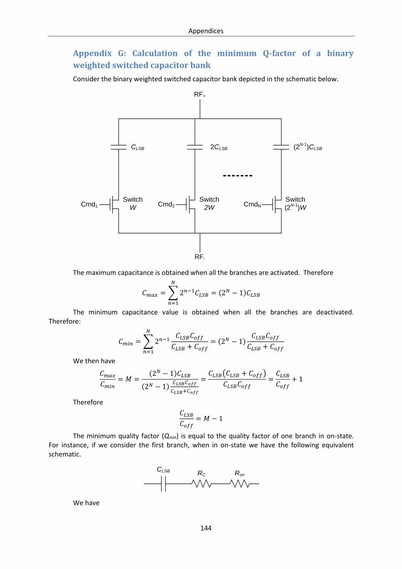
Appendices
144
Appendix G: Calculation of the minimum Q-factor of a binary
weighted switched capacitor bank
Consider the binary weighted switched capacitor bank depicted in the schematic below.
The maximum capacitance is obtained when all the branches are activated. Therefore
𝐶𝑚𝑎𝑥 = ∑2𝑛−1𝐶𝐿𝑆𝐵
𝑁
𝑛=1
= (2𝑁 − 1)𝐶𝐿𝑆𝐵
The minimum capacitance value is obtained when all the branches are deactivated. Therefore:
𝐶𝑚𝑖𝑛 = ∑2𝑛−1𝐶𝐿𝑆𝐵𝐶𝑜𝑓𝑓
𝐶𝐿𝑆𝐵 + 𝐶𝑜𝑓𝑓
𝑁
𝑛=1
= (2𝑁 − 1)𝐶𝐿𝑆𝐵𝐶𝑜𝑓𝑓
𝐶𝐿𝑆𝐵 + 𝐶𝑜𝑓𝑓
We then have
𝐶𝑚𝑎𝑥𝐶𝑚𝑖𝑛
= 𝑀 =(2𝑁 − 1)𝐶𝐿𝑆𝐵
(2𝑁 − 1)𝐶𝐿𝑆𝐵𝐶𝑜𝑓𝑓
𝐶𝐿𝑆𝐵+𝐶𝑜𝑓𝑓
=𝐶𝐿𝑆𝐵(𝐶𝐿𝑆𝐵 + 𝐶𝑜𝑓𝑓)
𝐶𝐿𝑆𝐵𝐶𝑜𝑓𝑓=𝐶𝐿𝑆𝐵𝐶𝑜𝑓𝑓
+ 1
Therefore
𝐶𝐿𝑆𝐵𝐶𝑜𝑓𝑓
= 𝑀 − 1
The minimum quality factor (Qmin) is equal to the quality factor of one branch in on-state. For instance, if we consider the first branch, when in on-state we have the following equivalent schematic.
We have
CLSB
Switch
WCmd1
2CLSB
Switch
2W
RF+
RF-
Cmd2
(2N-1
)CLSB
Switch
(2N-1
)WCmdN
CLSB RC Ron

Appendices
145
𝑅𝐶 =1
2𝜋𝑓0𝑄𝐶𝐶𝐿𝑆𝐵=
1
𝜔0𝑄𝐶𝐶𝐿𝑆𝐵
The minimum quality factor is then
𝑄𝑚𝑖𝑛 =1
𝜔0(𝑅𝐶 + 𝑅𝑜𝑛)𝐶𝐿𝑆𝐵=
1
𝜔0 (1
𝜔0𝑄𝐶𝐶𝐿𝑆𝐵+ 𝑅𝑜𝑛)𝐶𝐿𝑆𝐵
=1
1
𝑄𝐶+𝜔0𝑅𝑜𝑛𝐶𝐿𝑆𝐵
=𝑄𝐶
1 + 𝜔0𝑄𝐶𝑅𝑜𝑛𝐶𝐿𝑆𝐵
=𝑄𝐶
1 + 𝜔0𝑄𝐶𝑅𝑜𝑛𝐶𝐿𝑆𝐵𝐶𝑜𝑓𝑓
𝐶𝑜𝑓𝑓
=𝑄𝐶
1 + 𝜔0𝑄𝐶𝑅𝑜𝑛𝐶𝑜𝑓𝑓𝐶𝐿𝑆𝐵
𝐶𝑜𝑓𝑓
And finally
𝑄𝑚𝑖𝑛 =𝑄𝐶
1 + 𝜔0𝑄𝐶𝐹𝑂𝑀(𝑀 − 1)

Appendices
146
147
Figure index Figure 1: E-UTRA frequency bands (Uplink). .................................................................................... 13
Figure 2: Multiband 2G/3G/4G FEM for FDD applications. ............................................................. 14
Figure 3: Converged PA Architecture............................................................................................... 15
Figure 4: Multimode PA with saturated and linear operating modes [Kang08]. ............................. 16
Figure 5: Reconfigurable multimode PA with transistor sizing and reconfigurable matching
network [Kang13].................................................................................................................................. 17
Figure 6: Simplified schematic of a multiband saturated PA [Aref12]. ........................................... 18
Figure 7: PAE vs. Output Power (Pout) for a traditional PA architecture. ...................................... 18
Figure 8:PAE evolution vs. Output Power in a multi-power mode PA ............................................ 19
Figure 9: PA architecture with power transistor re-sizing. .............................................................. 20
Figure 10: PA stage bypass using line (left) or switch (right). .......................................................... 20
Figure 11:PAE evolution vs. Output Power in a traditional Power Amplifier .................................. 21
Figure 12: Block schematic of high efficiency PA architecture [ref] ................................................ 22
Figure 13: Block schematic of Envelope Tracking Power Amplifiers ............................................... 23
Figure 14: General schematic of the Envelope Elimination and Restoration Power Amplifier ....... 23
Figure 15: Block schematic of Doherty Amplifiers ........................................................................... 24
Figure 16: Passive Load Modulation Power Amplifier block schematic .......................................... 25
Figure 17: Used technologies in high performance FEM [ASN13]. .................................................. 27
Figure 18: Cross-section of a LDMOS transistor. ............................................................................. 28
Figure 19: Simplified structure of a high Q inductor (left) and compact inductor (right)
implemented with 3 metal layers and 1 turn per metal level. ............................................................. 28
Figure 20: MIM capacitor (left) and interdigitated MOM capacitor (right). ................................... 29
Figure 21: Simplified Cross-section view of a TSV connected to the source of a MOS transistor. .. 30
Figure 22: Gain, ACPR and power added efficiency performance of a 3G power amplifier ........... 36
Figure 23: Schematic representation of the power flowing in and out of a power amplifier. ........ 36
Figure 24: Power amplifier with source and load impedances. ...................................................... 37
Figure 25: Output Power (left) and Power Gain (right) versus Input Power of a medium power
amplifier. ............................................................................................................................................... 38
Figure 26: Illustration of the inter-modulation distortion of a power amplifier. ............................ 39
Figure 27: Two tone PA response showing 3rd Order Inter-Modulation Distortion ........................ 39
Figure 28: Constellation diagrams of a GMSK signal (left) and QPSK signal (right) ......................... 40
Figure 29: Spectrum of 3G signal after amplification showing spectral re-growth ......................... 41
Figure 30: Constellation of a QPSK signal after amplification through non-linear PA ..................... 42
Figure 31: LDMOS transistor model used in the study. ................................................................... 43

Figure index
148
Figure 32: Linearized IDS vs.VDS characteristic (solid lines) and load line (dotted line) of a common
source LDMOS transistor. ..................................................................................................................... 44
Figure 33: LDMOS transistor model used for the study on operating classes................................. 45
Figure 34: Input and output waveforms for Class A, AB, B and C .................................................... 46
Figure 35: Response of the LDMOS transistor model, linear model and quadratic model. ............ 47
Figure 36: Comparison of the drain efficiency obtain with both model according to the class using
the linear model (red dashed line) and quadratic model (solid blue line). .......................................... 49
Figure 37: Calculated first 5 harmonic components of sinusoidal classes using the linear model
(left) and quadratic model (right) versus the conduction angle Φ....................................................... 50
Figure 38: Power device sizing methodology and LDMOS transistor model. .................................. 52
Figure 39: Required LDMOS transistor width and optimal load resistance versus saturated power
.............................................................................................................................................................. 53
Figure 40: Load Pull contours for power gain (Gp) and power added efficiency(PAE) characteristics
.............................................................................................................................................................. 54
Figure 41: Simulated power added efficiency and power gain of the power cell ........................... 55
Figure 42: Linear PA design flowchart ............................................................................................. 56
Figure 43: Sweet spot of a PA under 2-tone excitation ................................................................... 57
Figure 44: Simulated ACLR performance of the Class F power stage under Rel99 signal. .............. 58
Figure 45: Simulated ACLR performance of the Class F power stageunder20MHz LTE signal ........ 58
Figure 46: matching network design methodology ......................................................................... 59
Figure 47: Intermediate impedances in a multi-cell network ......................................................... 60
Figure 48: Tunable capacitor elementary cell ................................................................................. 61
Figure 49: Schematic of a switched capacitor bank. ....................................................................... 62
Figure 50:Voltage distribution across a capacitor branch in on-state ............................................. 63
Figure 51:Voltage distribution across a capacitor branch in off-state ............................................ 64
Figure 52: Example of a SPnT architecture ...................................................................................... 64
Figure 53: Equivalent schematics of the SP1T in “on” mode (upper) and “off” mode (bottom) ... 65
Figure 54: Insertion Loss and isolation of SP1T ............................................................................... 66
Figure 55: Equivalent schematics of the activated throw (left) and deactivated throws (right) of a
SPnT....................................................................................................................................................... 66
Figure 56: Insertion loss (left) and isolation (right) of a SPnT for n=2 to 5 ...................................... 67
Figure 57: Block schematic of the reconfigurable MMPA. .............................................................. 70
Figure 58: Macro-band division. ...................................................................................................... 71
Figure 59: Reconfigurable power stage. .......................................................................................... 72
Figure 60: Simulated optimal load impedance versus frequency in saturated mode (top) and
linear mode (bottom). .......................................................................................................................... 73
Figure 61: Power cell with input switch. .......................................................................................... 74
Figure index
149
Figure 62: Equivalent interconnection network of the power cell in saturated mode. .................. 74
Figure 63: Equivalent interconnection network of the power cell in linear mode.......................... 75
Figure 64: Simulated PAE and power gain of the power cell in saturated mode. ........................... 75
Figure 65: Simulated PAE and power gain (left) ACPR (right) of the power cell in linear mode. .... 76
Figure 66: output matching network architecture .......................................................................... 78
Figure 67: Simulated input impedance of the output matching network normalized by the optimal
load impedance in each mode and band (Zref). ..................................................................................... 79
Figure 68: Simulated insertion loss of the output matching network as a function of frequency .. 79
Figure 69: Harmonic termination using a series LC resonator ........................................................ 80
Figure 70:Insertion Losses of the matching network combined with the 2nd harmonic trap ........ 81
Figure 71: Simulated impedance presented to the power stage by the output matching network
and harmonic trap at the fundamental, 2nd harmonic and 3rd harmonic frequencies normalized by
the optimal load impedance in each mode, band and harmonic (Zref). ................................................ 81
Figure 72: Efficiency (left) and ACPR (right) responses of the power stage for a Release’99 signal
at 800MHz with and without harmonic trap at the 3rd harmonic ....................................................... 82
Figure 73: 3rd harmonic termination using a second series LC resonator ...................................... 82
Figure 74: Impedance presented to the power stage by the output matching network and
harmonic traps at the fundamental, 2nd harmonic and 3rd harmonic frequencies ............................ 83
Figure 75: Insertion losses of the OMN combined with the 2nd and 3rd harmonic traps .............. 83
Figure 76: Schematic of the SP4T at the output of the reconfigurable power amplifier ................ 84
Figure 77: Impedance presented to the power stage by the combination of output matching
network, harmonic traps and SP4T at the fundamental, 2nd harmonic and 3rd harmonic frequencies.
.............................................................................................................................................................. 85
Figure 78: Insertion losses of the full matching network in each mode and frequency band ........ 85
Figure 79: Schematic of a tunable capacitor ................................................................................... 86
Figure 80: Minimum driver drain efficiency as a function of the inter-stage matching network
insertion loss(ILIntMN) in saturated mode ............................................................................................... 88
Figure 81: Schematic of the driver stage with RC feedback ............................................................ 89
Figure 82: Topology of the input matching network ....................................................................... 89
Figure 83: S11 (left) and insertion loss (right) of the input matching network for the different
modes and bands .................................................................................................................................. 90
Figure 84: Inter-stage matching network topologies. ..................................................................... 91
Figure 85: Insertion loss (top) and impedances seen at the input (bottom) ................................... 91
Figure 86: Implementation of a tunable inductor ........................................................................... 92
Figure 87: Block schematic of the implementation of the MMPA architecture. ............................. 93
Figure 88: Photographs of the two circuits: PA (a) and OMN (b) .................................................... 93
Figure 89: Photograph of the test board ......................................................................................... 94
Figure 90: Photograph of the test bench for reconfigurable MMPA characterization ................... 95

Figure index
150
Figure 91: Measured (blue) vs. simulated (red) S-Parameters of the MMPA in linear mode (left)
and saturated mode (left) at 900MHz. ................................................................................................. 95
Figure 92: CW measurements of the PA IC in saturated mode. ...................................................... 96
Figure 93: CW measurements of the PA IC in linear mode. ............................................................ 96
Figure 94: Measured insertion loss in each mode (Linear Mode at 700MHz (circles), at 800MHz
(squares), at 900MHz (diamond) and saturated mode at 800MHz (triangle) and at 900MHz (reversed
triangle)) ................................................................................................................................................ 97
Figure 95: Retro-simulated (blue dotted line) vs. measured IL of the OM in saturated mode at
800MHz. ................................................................................................................................................ 98
Figure 96: Measured (blue dotted lines) vs. simulated (red solid lines) input impedance of the
OMN IC in its different configurations (real part in circles, imaginary part in squares). ...................... 98
Figure 97: Measured PAE and power gain under CW signal .......................................................... 99
Figure 98: PA efficiency for fixed supply and load and , ET and LM configurations ...................... 103
Figure 99: Amplitude (left) and phase (right) response of the power cell for fixed supply and load
impedance (black dashed line), ET (blue dotted line) and LM (red solid line) configurations. .......... 105
Figure 100: Efficiency (top left), gain (bottom left) and phase (bottom right) comparison between
the stand alone cell, ET power cell with maximum efficiency shaping and ET power cell with isogain
shaping. ............................................................................................................................................... 106
Figure 101: Simulated performance of the ET power cell with a Release’99 signal at 835MHz. .. 107
Figure 102: Simulated performance of the 18dB Isogain ET power cell stimulated with a 20MHz
bandwidth (100 RB) LTE signal at 835MHz. ........................................................................................ 108
Figure 103: Efficiency (top left), gain (bottom left) and phase (bottom right) comparison between
the stand alone cell, LM power cell with maximum efficiency trajectory and LM power cell with
isogain trajectory. ............................................................................................................................... 109
Figure 104: Simulated performance of the 18dB Isogain LM power cell stimulated with a
Release’99 signal at 835MHz. ............................................................................................................. 110
Figure 105: Power added efficiency after load pull simulations (a) and load trajectory for optimal
efficiency (b)........................................................................................................................................ 111
Figure 106: Simplified schematic of the load modulation architecture ........................................ 111
Figure 107: Schematic and simulated states of the tunable matching network (green), Load
trajectory (orange) in a smith chart referenced by the optimal load impedance after the fixed
matching network ............................................................................................................................... 112
Figure 108: Schematic of a binary weighted switched capacitor array ......................................... 112
Figure 109: Schematic of binary weighted switched capacitor bank used as a tunable capacitor.
............................................................................................................................................................ 113
Figure 110: Minimum quality factor of the binary weighted switched capacitor bank according to
its tuning ratio and frequency............................................................................................................. 114
Figure 111: Simulated capacitance and quality factor of a tunable capacitor of the TMN for the 32
control states ...................................................................................................................................... 115

Figure index
151
Figure 112: Microphotograph of the TMN die .............................................................................. 115
Figure 113: Simulated insertion losses of the Tunable Matching Network in a Continuous Wave
simulation ........................................................................................................................................... 116
Figure 114: Simulated energy efficiency of the line-up as a function of output power in a
Continuous Wave simulation .............................................................................................................. 116
Figure 115: Photograph of the test board (left) with a zoom on the Power Cell and TMN circuits
(right) .................................................................................................................................................. 117
Figure 116: Comparison between measured and simulated S parameters .................................. 117
Figure 117: Measured PA efficiency with passive load modulation .............................................. 118

Figure index
152
153
Table index Table 1: Characteristics of TX signals for GSM handsets. ................................................................ 11
Table 2: Characteristics of TX signal for 3G handsets. ..................................................................... 12
Table 3: Bandwidth and Resource Blocks for LTE signals. ............................................................... 12
Table 4: Characteristics of TX signal for 4G handsets. ..................................................................... 12
Table 5: Performance of commercial “Mode Specific” Power Amplifiers. ...................................... 15
Table 6: Performances of converged 2G/3G PA with support of bands 5 and 8 [Kang13]. ............ 15
Table 7: State-of-the-art of reconfigurable multimode PA [Kang08] [Kang13]. .............................. 17
Table 8: State-of-the-art PA architecture with power transistor re-sizing. ..................................... 20
Table 9: State-of-the-art of Stage-bypass PA architectures. ........................................................... 21
Table 10: High efficiency PA architecture with supply/load modulation. ....................................... 26
Table 11: Technology Comparison. .................................................................................................. 26
Table 12: Aperture and conduction angles and DC bias voltage for classes A, AB, B and C ............ 46
Table 13: DC components of each signals ....................................................................................... 48
Table 14: Fundamental components of each signals ...................................................................... 48
Table 15: Harmonic components of each signals ............................................................................ 48
Table 16: Expression of η0 ................................................................................................................ 49
Table 17: DC components of voltage and current in Class F and Class F-1 ....................................... 51
Table 18: Fundamental components of voltage and current in Class F and Class F-1 ...................... 51
Table 19: Exact and approximated η0 for classes deep AB, F and F-1, for each current model ...... 51
Table 20: LDMOS transistor sizing for Class-F-1 PA design .............................................................. 55
Table 21: Optimal source and load impedances after source and load pull ................................... 55
Table 22: Power device performance at Sweet Spot ....................................................................... 57
Table 23: Source and load impedances after source and load pull ................................................. 57
Table 24: Targeted performance in each mode. ............................................................................. 70
Table 25: Required performances of the power stage in each mode. ............................................ 72
Table 26: Simulated performance of the power stage in saturated and linear modes ................... 76
Table 27: required Q-Factor as a function of the frequency band. ................................................. 77
Table 28: Optimal load impedance in saturated and linear modes. ............................................... 77
Table 29: Component values of the output matching network ...................................................... 78
Table 30: Capacitor values. .............................................................................................................. 78
Table 31: Simulated performance in saturated and linear mode .................................................... 83
Table 32: Switches sizes of the SP4T................................................................................................ 84
Table index
154
Table 33: Simulated performance of the output sub-assembly including the SP4T in saturated and
linear mode ........................................................................................................................................... 85
Table 34: State of the switches according to the capacitance value ............................................... 86
Table 35: Capacitances values and increments for the output matching network and the 2nd
harmonic trap ....................................................................................................................................... 86
Table 36: Required component parameters for the realization of C1 in the output matching
network ................................................................................................................................................. 87
Table 37: Required number of MOS transistor required in stacks in the output subassembly ...... 87
Table 38: Simulated performance in saturated an linear mode ...................................................... 87
Table 39: Requirements of the driver stage according to the Interstage matching insertion loss . 88
Table 40: IMN Capacitor value according to the mode for a 4.1nH inductance ............................. 90
Table 41: Simulated performance of the driver stage with input matching in saturated and linear
modes.................................................................................................................................................... 90
Table 42: Component values of the inter-stage matching network ................................................ 92
Table 43: Simulated performance of the reconfigurable MMPA. ................................................... 94
Table 44: Performance summary and comparison with the state of the art. ................................. 96
Table 45: OMN IC performance summary and comparison with other works................................ 99
Table 46: Simulated performance of the ET PA with a Rel'99 signal @ 835MHz (ACPR = -40dBc).
............................................................................................................................................................ 107
Table 47: Simulated performance of the ET PA with a 20MHz LTE signal @ 835MHz
(ACPR = -35dBc). ................................................................................................................................. 108
Table 48: Comparison between the proposed amplifier and [5] .................................................. 118

155
List of acronyms and abbreviations
ACPR Adjacent Channel Power Ratio
ACLR Adjacent Channel Leakage Ratio
AltCPR Alternate Channel Power Ratio
AltCLR Alternate Channel Leakage Ratio
AM Amplitude Modulation
AM/AM Amplitude to Amplitude distortion
AM/PM Amplitude to Phase distortion
AMPS Advanced Mobile Phone System
BAW Bulk Acoustic Wave
BW Bandwidth
BO Back-off
CDMA Code Division Multiple Access
CMOS Complementary Metal Oxide Semiconductor
DC Direct Current
DPX Duplex Filter
EDGE Enhanced Data-rates for GSM Evolution
EER Envelope Elimination and Restoration
ETPA Envelope Tracking PA
ETSI European Telecommunications Standard Institute
E-UTRA Evolved Universal Terrestrial Radio Access
EVM Error Vector Magnitude
FEM Front-End Module
FDD Frequency-Division Duplexing
FRN Frequency Reconfigurable Network
GaAs Gallium Arsenide
GSM Global System for Mobile
GMSK Gaussian Minimum Shift Keying
GPRS General Packet Radio Service
HB High Band
HEPA High Efficiency Power Amplifier
HSPA High Speed Packet Access
HSPA+ Evolved HSPA
HSDPA High Speed Packet Downlink Access
HSUPA High Speed Packet Uplink Access
IEEE Institute of Electrical and Electronics Engineers
IL Insertion Loss
IMD3 3rd order Inter-Modulation product
IS-95 Interim Standard 95
LB Low Band
LDMOS Laterally Diffused Metal Oxide Semiconductor (transistor)
Lin. Linear (Mode)
LNA Low Noise Amplifier
LTE Long Term Evolution
LTE-A LTE-Advanced
LMPA Load Modulation Power Amplifier
MB Mid-band
MIM Metal Insulator Metal (capacitor)
MIMO Multiple Input Multiple Output
MMPA Multi-mode multi-band power amplifier
MOM Metal Oxide Metal (capacitor)
MOS Metal Oxide Semiconductor (transistor)
OFDMA Orthogonal Frequency Division Multiple Access
OMN Output Matching Network
PA Power Amplifier
PAM Power Amplifier Module
PAE Power Added Efficiency
PAPR Peak to Average Power Ratio
PM Phase Modulation
Q Quality factor
QAM Quadrature Amplitude Modulation
QPSK Quadrature Phase Shift Keying
RB Resource Block
RF Radiofrequency
RX Reception Path
RMN Reconfigurable Matching Network
Sat. Saturated (Mode)
SAW Surface Acoustic Wave
Si Silicon
SMD Surface Mounted Device
SOI Silicon on Insulator
SPnT Single Pole n Throw(s)
TACS Total Access Communication System
TDD Time-Division Duplexing

List of acronyms and abbreviations
156
TDMA Time Division Multiple Access
TMN Tunable Matching Network
TSV Through Silicon Via
TRX Transmission / Reception Path
TX Transmission Path
UMTS Universal Mobile Telecommunications System
VHB Very High Band
VLB Very Low Band
VLSI Very Large Scale Modulation
VoIP Voice over Internet Protocol
W-CDMA Wideband Code Division Multiple Access
WiMAX World interoperability for Microwave Access
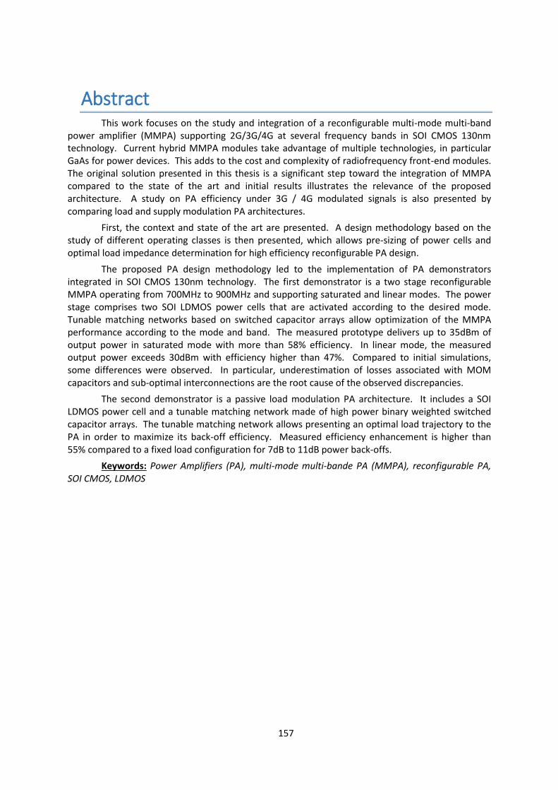
157
Abstract This work focuses on the study and integration of a reconfigurable multi-mode multi-band
power amplifier (MMPA) supporting 2G/3G/4G at several frequency bands in SOI CMOS 130nm technology. Current hybrid MMPA modules take advantage of multiple technologies, in particular GaAs for power devices. This adds to the cost and complexity of radiofrequency front-end modules. The original solution presented in this thesis is a significant step toward the integration of MMPA compared to the state of the art and initial results illustrates the relevance of the proposed architecture. A study on PA efficiency under 3G / 4G modulated signals is also presented by comparing load and supply modulation PA architectures.
First, the context and state of the art are presented. A design methodology based on the study of different operating classes is then presented, which allows pre-sizing of power cells and optimal load impedance determination for high efficiency reconfigurable PA design.
The proposed PA design methodology led to the implementation of PA demonstrators integrated in SOI CMOS 130nm technology. The first demonstrator is a two stage reconfigurable MMPA operating from 700MHz to 900MHz and supporting saturated and linear modes. The power stage comprises two SOI LDMOS power cells that are activated according to the desired mode. Tunable matching networks based on switched capacitor arrays allow optimization of the MMPA performance according to the mode and band. The measured prototype delivers up to 35dBm of output power in saturated mode with more than 58% efficiency. In linear mode, the measured output power exceeds 30dBm with efficiency higher than 47%. Compared to initial simulations, some differences were observed. In particular, underestimation of losses associated with MOM capacitors and sub-optimal interconnections are the root cause of the observed discrepancies.
The second demonstrator is a passive load modulation PA architecture. It includes a SOI LDMOS power cell and a tunable matching network made of high power binary weighted switched capacitor arrays. The tunable matching network allows presenting an optimal load trajectory to the PA in order to maximize its back-off efficiency. Measured efficiency enhancement is higher than 55% compared to a fixed load configuration for 7dB to 11dB power back-offs.
Keywords: Power Amplifiers (PA), multi-mode multi-bande PA (MMPA), reconfigurable PA, SOI CMOS, LDMOS
158
Résumé Cette thèse porte sur l’étude et l’intégration en technologie SOI CMOS d’un circuit
amplificateur de puissance multimode multibande (MMPA) reconfigurable capable d’adresser les modes 2G/3G/4G sur plusieurs bandes de fréquences. Les modules MMPA actuels (modules hybrides) reposent sur l’utilisation de plusieurs technologies, en particulier la technologie GaAs en ce qui concerne les chaines d’amplification, et représentent une part importante du coût et de l’encombrement d’une tête d’émission radiofréquences. La solution originale proposée dans cette thèse représente une avancée significative en termes d’intégration par rapport à l’état de l’art et les premiers résultats mesurés démontrent la pertinence de l’architecture proposée. Une étude sur l’optimisation du rendement énergétique au niveau de l’étage de puissance en présence de signaux modulés en amplitude et phase de type 3G et 4G est également proposée. Cette étude adresse les potentialités des techniques de modulation de la charge et de l’alimentation et permet de comparer les deux approches.
Après une présentation du contexte et de l’état de l’art, une méthodologie de conception originale reposant sur l’étude de différentes classes de fonctionnement est proposée. Cette méthodologie permet en particulier de pré-dimensionner les cellules de puissance reconfigurables ainsi que leurs impédances de source et de charge en fonction des contraintes de puissance et de linéarité dans les différents modes pour avoir le meilleur rendement. Elle permet aussi de choisir les topologies de réseaux d’adaptation accordables pertinentes.
Ces études ont conduit à la réalisation de deux démonstrateurs intégrés en technologies SOI CMOS 130 nm. Le premier prototype est un amplificateur multimode et multibande reconfigurable à deux étages capable de fonctionner en mode saturé et en mode linéaire pour des bandes de fréquence situées entre 700MHz et 900MHz. L’architecture proposée est composée d’un étage de puissance reconfigurable constitué de deux cellules de puissance de type LDMOS pouvant être activées ou non en fonction du mode adressé. Différents réseaux d’adaptation accordables à base de capacités commutées utilisant des transistors NMOS à body flottant permettent une optimisation des performances du MMPA en fonction du mode et de la bande de fréquence. Avec ce prototype, des puissances de sortie de 35dBm en mode saturé et 30dBm en mode linéaire ont été mesurées avec des rendements correspondants supérieurs respectivement à 58% et 47%. Par rapport aux simulations initiales, des différences ont été observées puis analysées afin d’en identifier l’origine. Notamment, la surestimation du facteur de qualité des capacités MOM dans les réseaux de capacités commutées et des interconnections sous optimales sont la cause des écarts observés.
Le deuxième prototype est un amplificateur de puissance à modulation de charge passive intégrée. Cet amplificateur repose sur une cellule de puissance de type LDMOS associée à un réseau d’adaptation accordable à base de capacités commutées capables de supporter une puissance supérieure à 33dBm. Ce réseau permet de présenter à l’étage de puissance une trajectoire de charge optimale en fonction de la puissance de sortie. Avec ce prototype, une amélioration du rendement supérieure à 55% par rapport à la configuration utilisant une charge constante a été mesurée pour un recul en puissance compris entre 7dB et 11dB.
Mots clés : Amplificateurs de puissance (PA), PA multimode multibande (MMPA), PA reconfigurable, SOI CMOS, LDMOS