Embed Size (px)
Citation preview
High Efficiency SEPIC Converter For High Brightness Light
Emitting Diodes (LEDs) System
Yaxiao Qin
Thesis submitted to the faculty of the Virginia Polytechnic Institute and State
University in partial fulfillment of the requirements for the degree of
Master of Science
In
Electrical Engineering
Jih-Sheng Lai, Chair
Wensong Yu
Kathleen Meehan
August 17th, 2012
Blacksburg, Virginia
Keywords: SEPIC, Power Factor Correction, Light emitting diode, Electrolytic capacitor, Interleaved converter, Long lifetime LED driver
Copyright 2012, Yaxiao Qin
High Efficiency SEPIC Converter For High Brightness Light Emitting
Diodes (LEDs) System
Yaxiao Qin
ABSTRACT
This thesis presents an investigation into the characteristics of and driving methods
for light emitting diode (LED) lamp system. The characteristic of the light emitting
diode (LED) lamp is described and the requirements of the ballast for the light emitting
diode (LED) lamp are presented.
Although LED lamps have longer lifetime than fluorescent lamps, the short
lifetime limitation of LED driver imposed by electrolytic capacitor has to be resolved.
Therefore, an LED driver without electrolytic capacitor in the whole power conversion
process is preferred. A single phase, power factor correction converter without
electrolytic capacitors for LED lighting applications is proposed, which is working in
discontinuous conduction mode (DCM). Different with a conventional SEPIC converter,
the middle capacitor is replaced with a valley-fill circuit. The valley-fill circuit could
reduce the voltage stress of output diode and middle capacitor under the same power
factor condition, thus achieving higher efficiency. Instead of using an electrolytic
capacitor for the filter, a polyester capacitor of better lifetime expectancy is used.
An interleaved power factor correction SEPIC with valley fill circuit is proposed to
further increase the efficiency and to reduce the input and output filter size and cost.
The interleaved converter shows the features such as ripple cancellation, good thermal
distribution and scalability.

iii
Acknowledgements
With sincere gratitude in my heart, I would like to thank my advisor, Dr. Jason Lai,
for his guidance, encouragement and support throughout this work and my study here at
Virginia Tech. His extensive knowledge, broad vision, zealous research attitude and
creative thinking have been a source of inspiration for me. I was so lucky to have the
opportunity to pursue my graduate study as his student at the Future Energy Electronics
Center (FEEC).
I would like to express my appreciation to Dr. Wensong Yu. I am incredibly
fortunate to have had the opportunity to work with him. The experience working with
him is a great time period, which I will never forget. His guidance and patience during
my research are greatly appreciated.
I am also grateful to the other members of my advisory committee, Dr. Kathleen
Meehan for her valuable suggestions and numerous help.
It has been a great pleasure to work with so many talented colleagues in the FEEC. I
would like to thank Mr. Gary Kerr, Dr. Hao Qian, Dr. Chien-Liang Chen, Dr. Pengwei
Sun, Dr. Zheng Zhao, Mr. Wei-Han Lai, Mr. Hidekazu Miwa, Mr. Chris Hutchens, Mr.
Ahmed Koran, Mr. Daniel Martin, Mr. Bret Whitaker, Mr. Ben York, Mr. Cong Zheng,
and Mr. Zidong Liu for their helpful discussions, great supports and precious friendship.
This work was supported by National Semiconductor Corporation (Santa Clara, CA).
iv
TABLE OF CONTENTS
CHAPTER 1 OVERVIEW AND BACKGROUND OF RESEARCH ............................ 1
1.1 Introduction ......................................................................................................... 1
1.2 Light emitting diode (LED) Lamps..................................................................... 3
1.2.1 The Principle and Characteristic of Light emitting diode (LED) Lamps . 3
1.3 Ballasts for Light emitting diode (LED) Lamps ................................................. 7
1.3.1 Topology and Performance Requirements of Electronic Ballast Circuit . 7
1.3.2 A topology study of the existing LED driver. ........................................ 10
1.4 Organization of the Thesis ................................................................................ 11
CHAPTER 2 A SINGLE PHASE SEPIC WITH VALLEY FILLED CIRCUIT FOR
LED APPLICATION ...................................................................................................... 13
2.1 Introduction of SEPIC Converter ...................................................................... 13
2.2 Principle of DCM Operated SEPIC converter .................................................. 18
2.3 Proposed DCM Operated SEPIC derived converter ......................................... 19
2.3.1 Principle of Proposed DCM Operated SEPIC derived converter .......... 19
2.3.2 The Voltage and Current Stress of the devices and components. ........... 31
2.4 Experimental Results ........................................................................................ 32
2.5 Loss Distribution ............................................................................................... 36
2.5.1 Inductor Losses ...................................................................................... 37

v
2.5.2 MOSFET Losses .................................................................................... 38
2.5.3 Diode Losses .......................................................................................... 39
2.6 Chapter Summary ............................................................................................. 41
CHAPTER 3 INTERLEAVED SEPIC WITH VALLEY FILLED CIRCUIT FOR LED
APPLICATION ............................................................................................................... 42
3.1 Introduction of interleaving technique .............................................................. 42
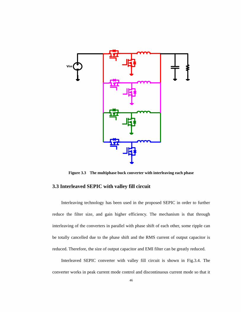
3.2 Review of Multi-Phase Buck for VR Application ............................................ 43
3.3 Interleaved SEPIC with valley fill circuit ......................................................... 46
3.4 Experimental Results for the proposed interleaved SEPIC with valley fill
circuit ...................................................................................................................... 49
3.5 Chapter Summary ............................................................................................. 54
CHAPTER 4 CONCLUSIONS AND SUGGESTIONS FOR FUTURE RESEARCH.. 55
4.1 Conclusions ....................................................................................................... 55
4.2 Contributions and Suggestions for Future Work ............................................... 56
Reference......................................................................................................................... 57
vi
List of Figures
Figure 1.1 Basic construction of High Brightness Philps LED ................................ 4 Figure 1.2 LED electrical model ............................................................................ 7 Figure 2.1 Offline SEPIC schematic .................................................................... 13 Figure 2.2 Bode plot of control to output transfer function of CCM SEPIC ....... 17 Figure 2.3 Proposed valley fill SEPIC PFC circuit .............................................. 19 Figure 2.4 The steady state current waveforms of proposed converter ............... 20 Figure 2.5 Equivalent circuit during different intervals ....................................... 22 Figure 2.6 Normalized input current versus ratio m ............................................ 25 Figure 2.7 The power factor as a function of Vin/(2Vc1+Vo) ................................. 26 Figure 2.8 The middle capacitor voltage over the ac line period ......................... 29 Figure 2.9 Input current(500mA/div) and input voltage (50V/div) ..................... 34 Figure 2.10 Gate driving signal (10V/div), output voltage(50V/div) .................. 34 Figure 2.11 Gate driving signal (10V/div), inductor L1 current(1A/div) and
voltage(100V/div) ........................................................................................... 35 Figure 2.12 Gate driving signal (10V/div), inductor L2 current(1A/div) and
voltage(100V/div) ........................................................................................... 35 Figure 2.13 Measured input current individual harmonics compared with IEC
61000-3-2 Class C standard ............................................................................ 36 Figure 2.14 The power loss distribution of the proposed SEPIC converter ............ 40 Figure 2.15 Efficiency curve at different load conditions....................................... 41 Figure 3.1 Single phase synchronous buck converter .......................................... 45 Figure 3.2 Single phase buck converter with paralleling devices ........................ 45 Figure 3.3 The multiphase buck converter with interleaving each phase ............ 46 Figure 3.4 Schematic diagram of proposed interleaved SEPIC with valley fill
circuit. ............................................................................................................. 47 Figure 3.5 The operating current and voltage waveforms ................................... 48 Figure 3.6 Input current(2A/div) and input voltage (50V/div) ............................ 50 Figure 3.7 Inductor L1a current(2A/div) and inductor L1b current(2A/div) .......... 50 Figure 3.8 Zoom in inductor L1a current(1A/div) and inductor L1b current(1A/div)
......................................................................................................................... 51 Figure 3.9 Zoom in inductor L2a current(1A/div) and inductor L2b current(1A/div)
......................................................................................................................... 51 Figure 3.10 Measured input current individual harmonics compared with IEC
61000-3-2 Class C standard ............................................................................ 52 Figure 3.11 Efficiency curve at different load conditions....................................... 54

vii
List of Tables
Table 2.1 Summary of selected components........................................................ 33 Table 2.2 Efficiency results at different load conditions ..................................... 40 Table 3.1 Summary of selected components........................................................ 52 Table 3.2 Efficiency results at different load conditions. .................................... 53
1
CHAPTER 1
OVERVIEW AND BACKGROUND OF RESEARCH
1.1 Introduction
Light or visible light is the electromagnetic radiation of a wavelength that is visible
to the human eye (about 400-700nm), or up to 380-750nm [1]. It is unthinkable if this
world had no solar energy for just a day. During the past 100 years, man has never given
up the search for effective light sources. The research of converting electric power to
light energy in a simple manner has driven the development of modern lamps in the past
decades [2]. Electrical lighting sources have been an important part in human being’s
daily life since Edison invented the first incandescent lamp in 1879 [3,4]. When the
fluorescent lamps were first developed in 1938, electrical lighting sources achieved a
milestone. From then on, a novel concept, ‘gas discharge lamp’ was proposed [5, 6], and
many new types of electrical lamps were invented after that, such as, high pressure
mercury lamps (HPM), high pressure sodium lamps (HPS), metal halide lamps (MH),
flash-lamps filled with inert gas [7, 8].
Nowadays lighting consumes approximately 10–15% of the global energy
requirement [9]. Given the increasing concerns about energy saving, the improvement
for the overall efficiency of lighting systems is of significant importance. Fluorescent
lamps are well known for decades to be an efficient light source, which are mainly used
for home and office lighting. Recently, a new type of lamps: light emitting diode (LED)
lamps are born. The LED lamps that are now available can reliably offer over 120

2
lumens from a one-watt device. Due to the high-efficiency, the LEDs are increasingly
attractive in the world, especially for industrial applications such as the street light
[9-11].
The major characteristics, which should be considered when choosing a lamp, are
the luminous efficacy, lifetime, and lumen depreciation. Luminous efficacy is the
measure of the lamp’s ability to convert input electric power, in watts, into output
luminous flux, in lumens, and is measured in lumens per watt (lumens/watt). The life of
a lamp is the number of hours it takes on average for 50% of lamps of the same kind to
fail. The lumen depreciation is the decrease in lumen output that occurs as a lamp is
operated [12].
Incandescent lamps (light bulbs) create light by running electricity through a thin
filament, thereby heating the filament to a very high temperature so that it glows to
produce visible light. The lifespan of an incandescent lamp is around 1,000 hours,
which is much shorter than that of other common used lamps such as either a
fluorescent lamp and LED lamp [9].
Fluorescent lamp is a gas-discharge lamp, which uses the electricity to excite
mercury vapor, then in turn to produce short-wave ultraviolet light. The ultraviolet light
is absorbed by a phosphor coating inside the lamp, causing it to produce visible light.
While the heat generated by fluorescent lamps is much less than its incandescent
counterpart, energy is still lost in generating the ultraviolet light and converting this
light into visible light. Fluorescent lamps have life spans around 10,000 to 20,000 hours.
[1, 12, 13]. Mercury has been used during the manufacturing of fluorescent lamp, which
3
is another disadvantage of the fluorescent lamp- safety issue.
1.2 Light emitting diode (LED) Lamps
1.2.1 The Principle and Characteristic of Light emitting diode (LED) Lamps
A light-emitting-diode (LED) is a semiconductor diode that emits light when an
electric current is applied in the forward direction of the device, as in the simple LED
circuit [14]. When the LED is forward biased, electrons recombine with electron holes
and release energy in the form of photons. This effect is the electroluminescence where
incoherent and narrow-spectrum light is emitted from the p-n junction in a solid state
material. A LED lamp is a type of solid state lighting (SSL) that uses light-emitting
diodes (LEDs) as the source of light, rather than electrical filaments, plasma (used in arc
lamps such as fluorescent lamps). An LED is usually a small area (less than 1 mm2)
light source, often with optics added directly on top of the chip to shape its radiation
pattern [15]. The color of the emitted light depends on the composition and condition of
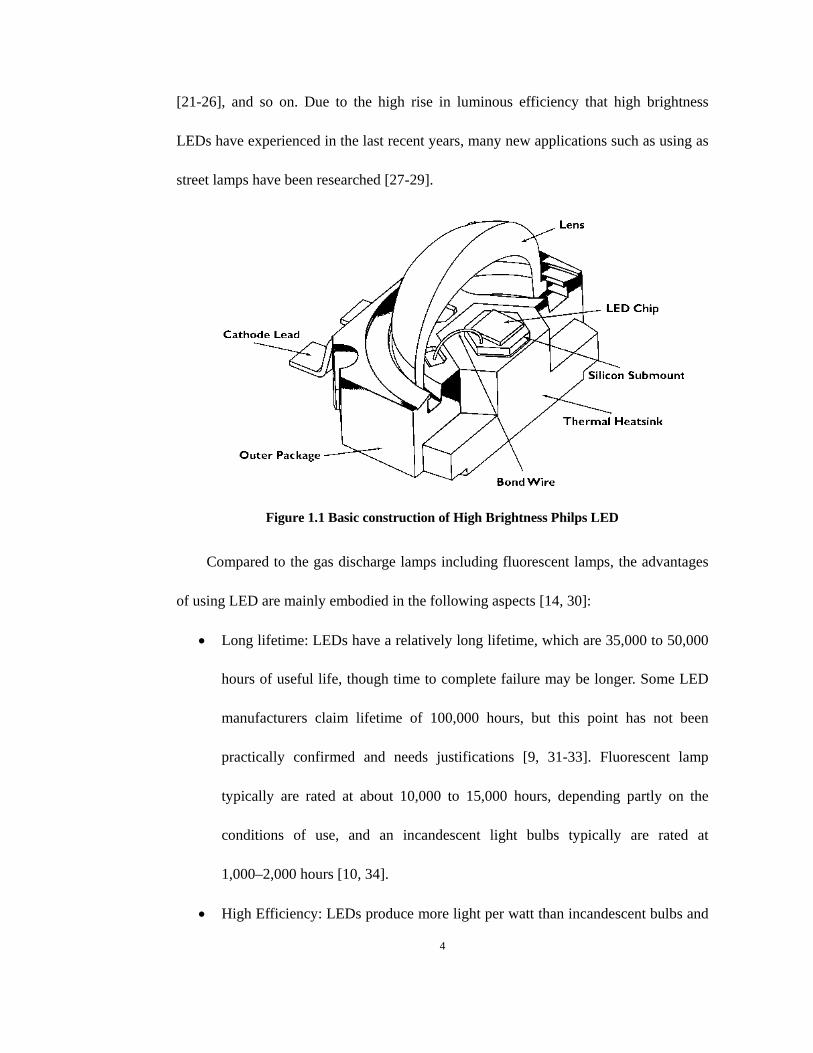
the semiconducting material used, and can be infrared, visible, or ultraviolet. The basic
construction of high power high brightness Philps LED is illustrated in Fig.1.1 [30]. It
includes the lens, LED chip, silicon submount, thermal heatsink, cathode lead, bond
wire and outer package [16].
Before the high brightness LEDs come into the market, the LEDs have been
widely used as indicator on electronic devices and battery powered applications for
decades [17]. These applications include cell phone handsets, digital still cameras,
automotive lighting [18, 19], emergency lighting [17, 20], and LCD backlighting
4
[21-26], and so on. Due to the high rise in luminous efficiency that high brightness
LEDs have experienced in the last recent years, many new applications such as using as
street lamps have been researched [27-29].
Figure 1.1 Basic construction of High Brightness Philps LED
Compared to the gas discharge lamps including fluorescent lamps, the advantages
of using LED are mainly embodied in the following aspects [14, 30]:
Long lifetime: LEDs have a relatively long lifetime, which are 35,000 to 50,000
hours of useful life, though time to complete failure may be longer. Some LED
manufacturers claim lifetime of 100,000 hours, but this point has not been
practically confirmed and needs justifications [9, 31-33]. Fluorescent lamp
typically are rated at about 10,000 to 15,000 hours, depending partly on the
conditions of use, and an incandescent light bulbs typically are rated at
1,000–2,000 hours [10, 34].
High Efficiency: LEDs produce more light per watt than incandescent bulbs and
5
fluorescent lamps. High brightness LEDs are now available that can offer over
120 lumens from a one-watt device, or much higher outputs at higher drive
currents [32].
Full Dimming: LEDs can very easily be dimmed, unlike fluorescent lamps.
There are two methods to dim LEDs lamps, include: pulse-width modulation
(PWM) dimming and analog dimming. Pulse-width modulation dimming turn
the light on and off very quickly at varying intervals. Pulse-width modulation
dimming is a more efficient means to modulate the intensity of the light
produced by the LED lamp [35, 36].
Small Size: LEDs are relatively small and are easily mounted onto printed
circuit boards, thus providing design flexibility, as they can be arranged in rows,
rings, cluster [9, 26].
Mercury-free: Based on the solid state lighting, LEDs contain no hazardous
mercury or halogen gases, unlike fluorescent and most HID gas discharge
technologies [13, 37]. GaN-based LEDs do not contain any heavy metals or
arsenic.
Although LED lamps have a lot of advantages over fluorescent lamps, the
disadvantages of using LEDs are also obvious:
High price: LEDs are currently relatively more expensive than the conventional
lighting technologies such as fluorescent lamps and HID lamp. However, when
considering the total cost including the replacement costs and the long lifetime
of LED lamps, LEDs are beginning to threaten the conventional lamps [14].
6
Temperature dependence: LED performance largely depends on the junction
temperature of LED and the ambient temperature of the operating environment.
Over-driving the LED in high ambient temperatures may result in overheating of
the LED package, eventually leading to the failure of LED. Adequate heatsink is
required to maintain long lifetime. This is especially important when considering
automotive applications where the device must operate over a large range of
temperatures [14, 18, 19].
Voltage sensitivity: A small voltage variation across the LEDs can lead to a large
change of the LEDs current. Therefore, LEDs should be supplied with current
source rather that voltage source to keep good performance of LEDs [38].
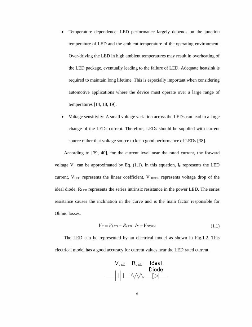
According to [39, 40], for the current level near the rated current, the forward
voltage VF can be approximated by Eq. (1.1). In this equation, IF represents the LED
current, VLED represents the linear coefficient, VDIODE represents voltage drop of the
ideal diode, RLED represents the series intrinsic resistance in the power LED. The series
resistance causes the inclination in the curve and is the main factor responsible for
Ohmic losses.
F LED LED F DIODEV V R I V (1.1)
The LED can be represented by an electrical model as shown in Fig.1.2. This
electrical model has a good accuracy for current values near the LED rated current.
7
Figure 1.2 LED electrical model
1.3 Ballasts for Light emitting diode (LED) Lamps
1.3.1 Topology and Performance Requirements of Electronic Ballast Circuit
Development of highly reliable and highly efficient electronic driver for Light
emitting diode (LED) has always been a hot research topic [9, 31, 41]. Generally, high
performance electronic driver design for Light emitting diode (LED) lamp should
satisfy the following requirements.
A. High Power Factor
In AC power system, the power factor is the ratio of the real power flowing to the
load to the apparent power of the converter. Due to the non-linear load in the circuit,
which distorts the wave shape of the current drawn from AC source, the real power can
be smaller than the apparent power and the power factor will be less than unity. LED
driver should incorporate power factor correction (PFC) techniques to improve the
consumption of electrical energy and to provide agreement with power quality standards
[42]. Nowadays, international standards has been published, which set requirements to
limit the magnitudes of harmonic currents injection into the public supply system.
Utilizing PFC not only ensures that the LED driver system compliance with the
specifications and standards [43, 44], but also improves the efficiency of the circuit. The
advantages of PFC include:
PFC can improve the voltage quality. Load with lower power factor draw more
current from the source than the load with a higher power factor. As power
8
factor decreases, the line current increases, which causes greater voltage drops in
the conductors and lower voltage delivered at the load. With PFC, the voltage
drops are reduced.
PFC can increase the efficiency of the LED driver. Both reactive power and
distortion power produce extra current, which increase the energy lost in the
driver and reduce the system efficiency.
PFC can increase the capacity of the LED driver. When the system’s power
factor is improved, the amount of reactive current is reduced and more power
can be drawn from the existing transformers and distribution lines.
Therefore, the exploration for PFC techniques in LED driver is highly desirable.
Generally, there are two methods for correcting the power factor and suppressing
harmonic distortion: the passive PFC method and the active PFC method. Passive PFC
uses only line-frequency reactive components, while the active PFC uses active devices
and high frequency reactive components.
In recent years, some topologies were developed to improve the power factor
performance of LED driver, such as a high power factor single stage SEPIC converter
working in DCM mode with universal input range [28, 31, 45, 46]. A quasi-active
power factor correction circuit for LED lamp with high efficiency is presented in [47]. A
single stage Flyback converter for hight brightness LED lamp is proposed to realize
PFC function in [48]. In those topologies, near-unity power factor is realized.
B. Dimming control
9
Another important feature for the LED driver is the dimming control. This feature
can optimize the consumption of electrical energy in LED lighting systems. For
applications such as LCD backlighting, dimming provides brightness and contrast
adjustment. Dimming white light LED systems can be accomplished by two techniques:
continuous current reduction and pulse-width-modulation (PWM) [22, 49, 50, 53, 54].
With analog dimming, 80% brightness can be achieved by supplying 80% of the
maximum current to the LED. Drawbacks of this method include LED color shift and
the need for an analog control signal [51]. PWM dimming is achieved by applying full
current to the LED at a reduced duty cycle. PWM is better because it can have a larger
dimming range, and also can solve the problem of color shift [36, 52].
C. High Efficiency and low cost
Due to the market pressure, it is desirable that the cost of LED driver as low as
possible [40]. In recent years, different topologies have been proposed to achieve high
efficiency of ballast circuits for LEDs. A synchronously-rectified (SR) flyback converter
with the proposed multi-function circuit is proposed in [29]. The proposed circuit can
detect the zero crossing of the current to realize zero current switching (ZCS) in order to
reduce switching loss. The proposed auxiliary circuit can work as a LC snubber and also
a housekeeping circuit. And hence, this converter has high efficiency all over the
operating and load range. In [55], a charge pump circuit for LED lamps is proposed.
The series-charge and parallel-discharge operation gives the efficiency better than the
conventional converters with ac line input since no magnetic components are adopted.
10
D. Long lifetime
Compared with other conventional lamps, an attractive feature of LEDs is
longevity, which is typically 100,000 hours [56],. The lifetime expectancy is much
longer than that of fluorescent lamps, which is typically 10,000 - 20,000 hours.
Although LED lamps have longer lifetime than fluorescent lamps, the short lifetime
limitation imposed by electrolytic capacitors in the LED driver has to be eliminated
[57,58].
1.3.2 A topology study of the existing LED driver.
A number of topologies have been used as high brightness LED driver. As LEDs
use low voltage DC source, hence the simple and common topologies can be used to
drive LEDs [9].
Flyback converter is one of the most frequently used candidate for the low power
LED driver especially when isolation is desirable [9, 20]. Working in discontinuous
conduction mode (DCM), the input harmonics normally meets the IEC1000-3-2
standards. A Boost converter is suitable for high efficiency, large LED string
applications where isolation is not mandatory [17, 24, 59, 60]. However, since boost
converter can only step up the voltage, it is suitable for large strings of LEDs in series
when the input is the AC mains.
The SEPIC converter has excellent power factor correction performance, but the
efficiency is not comparable with the other solutions [28, 46]. It does not have a
11
transformer and the associated leakage ring effect as in a flyback converter so the
voltage stress of active device in SEPIC is much lower than that in flyback converter.
[45] proposes an interleaved SEPIC converter for the offline LED lighting applications.
The magnetic components in this circuit are integrated to reduce cost and board space.
Cuk converter can drive LED at different input voltage range, from a universal
input voltage or battery. The input and output inductors create a smooth current at both
of the input and output of the converter, which can reduce the size and cost of EMI
components, while the buck, boost and buck-boost have at least one side with pulsed
current. [61] proposed a universal input digital controlled Cuk converter with both
nonpulsating input current and nonpulsating output current.
For medium power applications, symmetrical and asymmetrical half bridge
converters [31] can be used with high efficiency. The transformer runs in two quadrants,
indicating better utilization of the magnetic core, and smaller size of the magnetic
components for both the transformer and output inductor. Resonant converter has also
been used to drive LEDs. [41] proposes resonant converter with high power density and
very low switching losses for driving LEDs. Two stages converter for LED lamps can
be integrated into single stage to further reduce the cost and gain high efficiency. An
integrated single stage integrated Buck-Flyback Converter is proposed in [39].
1.4 Organization of the Thesis
The contents of this thesis are as follows:
In Chapter 1, a comprehensive overview on the lighting development will be

12
proposed. The characteristic of the light emitting diode (LED) lamp will be described.
The requirements of the ballast for the light emitting diode (LED) lamp will be
presented. The organization of the thesis will be described.
In Chapter 2, a single phase, power factor correction converter without electrolytic
capacitors for LED lighting applications is proposed, which is a modified SEPIC
converter working in discontinuous conduction mode (DCM). Different with a
conventional SEPIC converter, the middle capacitor is replaced with a valley-fill circuit.
The principle of the theory will be derived. The valley-fill circuit could reduce the
voltage stress of output diode and middle capacitor under the same power factor
condition, thus achieving higher efficiency. The proposed converter will be verified with
experimental results.
In Chapter 3, an interleaved power factor correction SEPIC with valley fill circuit
is proposed to further increase the efficiency and reduce the input and output filter size
and cost. The proposed interleaved converter shows the features such as ripple
cancellation, good thermal distribution and scalability. The proposed converter will be
verified with experimental results.
Chapter 4 is the summary of the thesis.
13
CHAPTER 2
A SINGLE PHASE SEPIC WITH VALLEY FILLED CIRCUIT
FOR LED APPLICATION
2.1 Introduction of SEPIC Converter
Single-ended primary-inductor converter (SEPIC) is a buck-boost derived
converter, which could step down and step up the input voltage. Different with
traditional buck-boost converter, SEPIC has non-inverting output. As shown in Fig 2.1 ,
the middle capacitor C1 works as coupling capacitor.
D1~D4AC
L1 Do
L2
C1
CoQ1
Figure 2.1 Offline SEPIC schematic
A SEPIC converter can work in continuous conduction mode (CCM) and
Discontinuous conduction mode (DCM). In CCM steady state, since the average voltage
across L1 and L2 is zero, the average voltage across coupling capacitor C1 is input
voltage (Vin). Since the average current flowing through C1 is zero, the inductor L2 is the
only source of output current. The average current through inductor L2 is the average
14
current of the load, which is independent of the input voltage.
In CCM, since the average voltage across the inductor L1 and L2 are both zero.
Therefore, the voltage of middle capacitor will follow the input voltage and the middle
capacitor has no low frequency energy storage function. Output capacitor takes the
function of low frequency energy storage. Therefore, the output capacitance need be
large to achieve a good output voltage regulation.
In CCM, since the voltage across the middle capacitor C1 is the input voltage Vin,
by applying voltage-second balance for inductor L1 (neglecting the forward voltage drop
of output diode), the output to input voltage ratio can be obtained as:
1o
in
V D
V D
(2.1)
Therefore, SEPIC is a buck-boost derived converter. The inductor L1 and Q1 create
the standard boost converter, which creates a voltage higher than input voltage and the
magnitude is determined by the duty cycle of the MOSFET Q1. Because the voltage
across C1 is Vin, the output voltage is VQ1-Vin. If VQ1 is larger than two times of input
voltage, the output voltage is greater than input voltage. Otherwise, it works as a step
down converter.
The middle capacitor of SEPIC could be usually non-polarized capacitor such as
Film capacitor because the voltage of the middle capacitor of SEPIC may reverse its
direction in every switching circle. However, in some cases, the electrolytic capacitor
could be used. In CCM, the electrolytic capacitor could be used since the capacitor
15
voltage ripple is relatively small.
In CCM SEPIC, since the average voltage across C1 is Vin. The magnitude of
voltage across L1 and L2 are the same so that they could be wound in the same core. And
the mutual inductance is zero if the polarity of the windings is correct. Therefore, the
two inductors are coupled and SEPIC can be seen as a similar flyback converter.
The small-signal model of SEPIC is required for building the SEPIC since the
compensation depends on the control characteristics of SEPIC. Accurate small signal
model for SEPIC is a difficult analytical task. There is a simplified analysis of the
SEPIC converter [102], which neglects the parasitic resistances of inductors and
capacitors.
Based on this simplified analysis, the control-to-output transfer function is
obtained as below:
2 221 1 1 2 2 1
2 21
2 2 2
2 21 1 1 2 2 2
( ) '(1 )(1 )
( ) 1 '
( ) '1 1
o
o o o o
L D C L L R D L Cs s s
v s R D L D D
d s D s s s sQ Q
(2.2)
where
12
2 1 1 12
1
( )'
o
o o
DL C C L C C
D
(2.3)
1 2
1 1 22'o
RQ
DL L
D
(2.4)
16
2
1 1 12 2 2
1
1 1
'
o
o oC C L C CLD D
(2.5)
2 21 1
2 1 2 22
( ) oo
o o
RQ
CL L
C
(2.6)
As shown in the Eq. (2.2), the SEPIC is fourth-order denominator converter. There are
two double poles in CCM SEPIC. For numerator, the first term is a single right half
plane zero (RHPZ). The second term is a complex RHPZ. RHPZs are a result of
converters where the response to an increased duty cycle is to initially decrease the
output voltage. When the power MOSFET is turned on, the inductor L1 is disconnected
to the load. This generates the first RHPZ. Therefore, the expression only depends on
the input inductor L1, the load resistor R, and the duty cycle, D. The complex RHP
zeros correspond to the fact that the second inductor is disconnected to the load when
the power MOSFET is turned on.
17
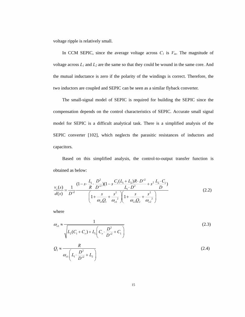
Figure 2.2 Bode plot of control to output transfer function of CCM SEPIC
Figure 2.2 shows the control to output transfer function in a typical CCM SEPIC
design. The red curve is the magnitude and the blue curve is the phase of the transfer
function. As shown in the Bode plot, there are two resonant frequency predicted in the
Eq. (2.2).
With low values of damping resistors, the converters has four poles (i.e. two
resonant frequency), and three right-half-plane-zeros. This generates large phase delay
after the second resonant frequency, which is due to the delay of second resonance and
the additional delay of the three RHPZ. Therefore, it is undesirable to control the
converter at a frequency beyond the second resonance. Therefore, the bandwidth of the
CCM SEPIC should be below the extreme phase delay of the second resonance
18
frequency.
2.2 Principle of DCM Operated SEPIC converter
As discussed above, the middle capacitor in CCM SEPIC has no line-frequency
energy storage function and the output capacitance need be large to store the line
frequency energy and suppress the low frequency voltage ripple for LED applications.
Therefore, it is very difficult to eliminate the electrolytic capacitors in CCM SEPIC with
low output voltage ripple, which is highly desirable for LED lighting application. For
DCM operation of SEPIC, according to [45, 62], there are two types of DCM operation.
The first one is defined as the current of the output diode is in continuous current mode
or not. When the output diode current is zero, the inductor L1 current and inductor L2
current are not zero and equal to each other. In this case, the middle capacitor still has
no low frequency energy storage function since its low frequency voltage still follows
the input voltage due to continuous current of inductor L1 and L2. For the second type of
DCM operation, which the inductor L1 current and inductor L2 current will both reach
zero in a switching period. After the inductor L1 current reaches zero, the voltage of
middle capacitor will not follow input voltage any more and will have the low
frequency energy storage function. Therefore, for the second type of DCM SEPIC, by
allowing a relative large voltage ripple across the middle capacitor, the capacitance
value of middle capacitor and output capacitor could be largely reduced thus eliminating
the electrolytic capacitors.

19
However, the DCM SEPIC PFC converter has some drawbacks. When the input
voltage is universal, the voltage stress for the middle capacitor and the output diode are
very high. Therefore, a valley-fill circuit is added to the DCM SEPIC PFC converter.
2.3 Proposed DCM Operated SEPIC derived converter
2.3.1 Principle of Proposed DCM Operated SEPIC derived converter
By replacing the middle capacitor with the valley fill circuit in the typical SEPIC
converter, a modified SEPIC is derived and is shown in Fig2.3. The valley fill circuit
contains two capacitors and three diodes. The two capacitors are charged in series and are
in parallel to feed the load. The converter operates at discontinuous current mode to
realize the power factor correction automatically.
Figure 2.3 Proposed valley fill SEPIC PFC circuit
Some basic assumptions are made for the analysis of the proposed converter.
1) The input voltage Vin is pure sinusoidal waveform.
20
2) The capacitance of middle capacitor C1 and C2 and output capacitor Co are large
enough so that in a switching period Ts, the voltage across these capacitors:
Vc1,Vc2, and Vo could be assumed to be constant.
3) All of the MOSFET and diodes, inductors, capacitors are ideal without any
parasitic components.
4) The inductors L1 and L2 both work in discontinuous conduction mode (DCM).
The current of inductor L1 reaches zero before current of inductor L2 reaches
zero.
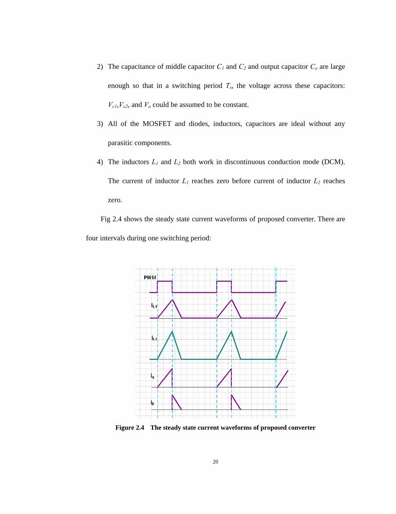
Fig 2.4 shows the steady state current waveforms of proposed converter. There are
four intervals during one switching period:
Figure 2.4 The steady state current waveforms of proposed converter
21
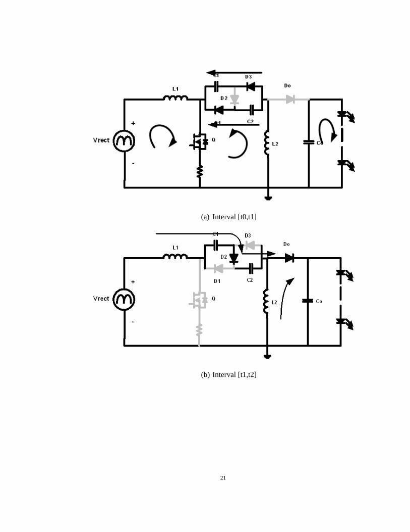
(a) Interval [t0,t1]
(b) Interval [t1,t2]
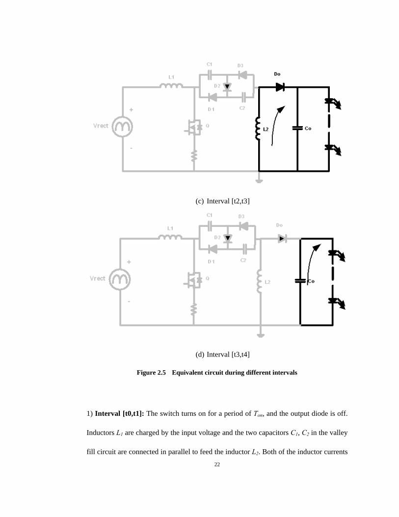
22
(c) Interval [t2,t3]
(d) Interval [t3,t4]
Figure 2.5 Equivalent circuit during different intervals
1) Interval [t0,t1]: The switch turns on for a period of Ton, and the output diode is off.
Inductors L1 are charged by the input voltage and the two capacitors C1, C2 in the valley
fill circuit are connected in parallel to feed the inductor L2. Both of the inductor currents
23
ramp up linearly. Therefore, the currents of L1 and L2 are given in (2.7), (2.8). The
MOSFET current is the sum of the two inductor currents, and is given in (2.9).
1
1
( ) inL
Vi t t
L
(2.7)
1
22
( ) cL
Vi t t
L
(2.8)
1 2( ) ( ) ( )Q L Li t i t i t (2.9)
2) Interval [t1,t2]: The switch turns off, and the diode is on for a period. Both inductor
currents freewheel through the diode and the inductor L1 and L2 currents ramp down
linearly. The two capacitors C1, C2 in the valley fill circuit are charged in series by the
inductor L1 current. At the end of this interval, the current of inductor L1 reaches zero. The
L1 current reduces according to (2.10). The L2 current reduces according to (2.11). The
diode current is the sum of both the inductor currents, as shown in (2.12).
11 1
1 1
2( ) in in c o
L s
V V V Vi t D T t
L L
(2.10) 1
2 12 2
( ) c oL s
V Vi t D T t
L L
(2.11)
1 2( ) ( ) ( )D L Li t i t i t (2.12)
3) Interval [t2,t3]: After the current of inductor L1 reaches zero, the inductor L2
continues to freewheel through the output diode. This interval does not end until the
current of inductor L2 reaches zero.
4) Interval [t3,t4]: Both the switch and the output diode are off for a period of Toff. The
output capacitor Co continues to charge the load.
Apply the voltage-second balance to the inductor L1:
1 2 1sin (2 sin )in l c o in lD V t D V V V t (2.13)
24
Since the proposed SEPIC PFC converter works in DCM, the inductor L1 and L2 peak
current in a switching cycle is derived as:
11_
1
sin sL pk in l
D Ti V t
L
(2.14)
12 _ 1
2
sL pk c
D Ti V
L
(2.15)
As shown in the equation(2.14), the peak current envelope of inductor L1 is
sinusoidal waveform.
The average inductor current in a switching cycle is derived as:
21
1_ ( ) 1_ 1 2
1
sin1
sin22 (1 )
2
l inL av t L pk
in ls b
c o
t V Di i D D
V tf L
V V
(2.16)
So the input current is:
21
( )
1
sin
sin2 (1 )
2
l inin t
in ls b
c o
t V Di
V tf L
V V
(2.17)
The input current is normalized with a base of 2
1
1
(1 )2 2
in in
s b c o
V D V
f L V V
for simpler
analysis. Then the normalized input current is obtained as:
*
( )
sin1
(1 sin )l
in tl
ti m
m t
(2.18)
where
12in
c o
Vm
V V
(2.19)
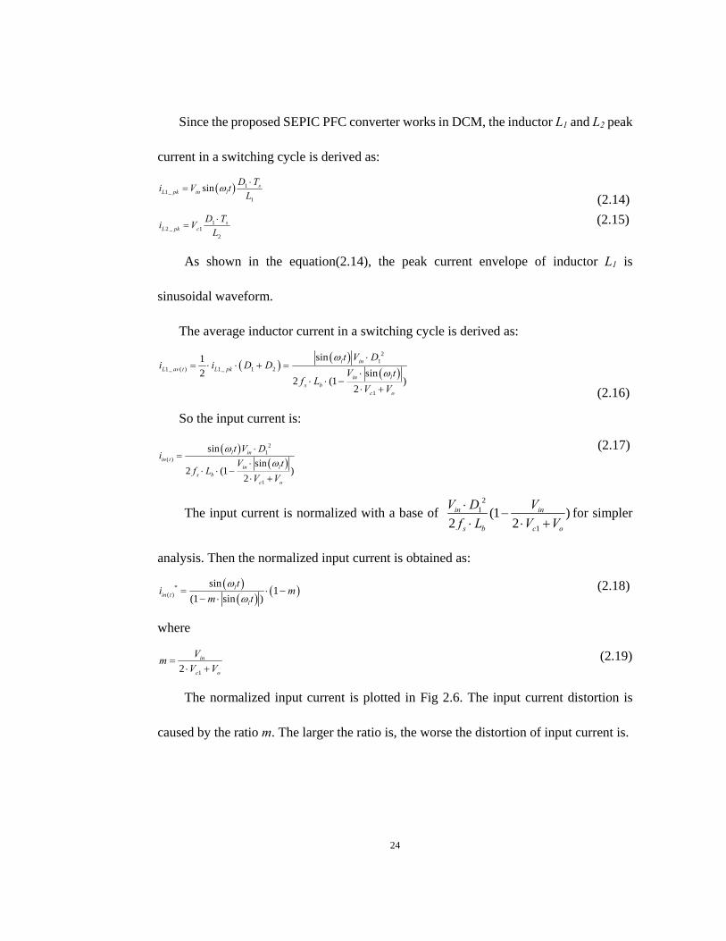
The normalized input current is plotted in Fig 2.6. The input current distortion is
caused by the ratio m. The larger the ratio is, the worse the distortion of input current is.
25
Figure 2.6 Normalized input current versus ratio m
As can be seen in the Fig 2.6 above, the ratio: Vin/(2Vc1+Vo) has a great influence on
the distortion of the input current. The higher ratio leads to a poorer distortion. This is
because if the ratio is higher, the falling time of input current is longer. Since the average
value of input current in falling time is not a sinusoid waveform. The falling time is
shorter and thus the input current waveform is closer to the sinusoid waveform.
The average of input power over one ac line cycle is obtained as:
2
1
0 0
1
sin1 1( ) ( ) ( ) sin
sin2 (1 )
2
l inin in in in l
in ls b
c o
t V DP i t v t dt V t dt
V tf L
V V
22 21
0
1
sin( )
2 sin(1 )
2
lin
b s in l
c o
tV D
L f V t
V V
(2.20)
26
The power factor is defined as the ratio of real power over apparent power. So the
power factor is obtained as:
2
0
0 1
22
0 0
1
sin2
sin1( ) ( ) 1
2
1 sin1( )sin
12
inin in
c o
RMS in
in
c o
tV t
i t v t dtV V
PFtV i t dt
V t
V V
(2.21)
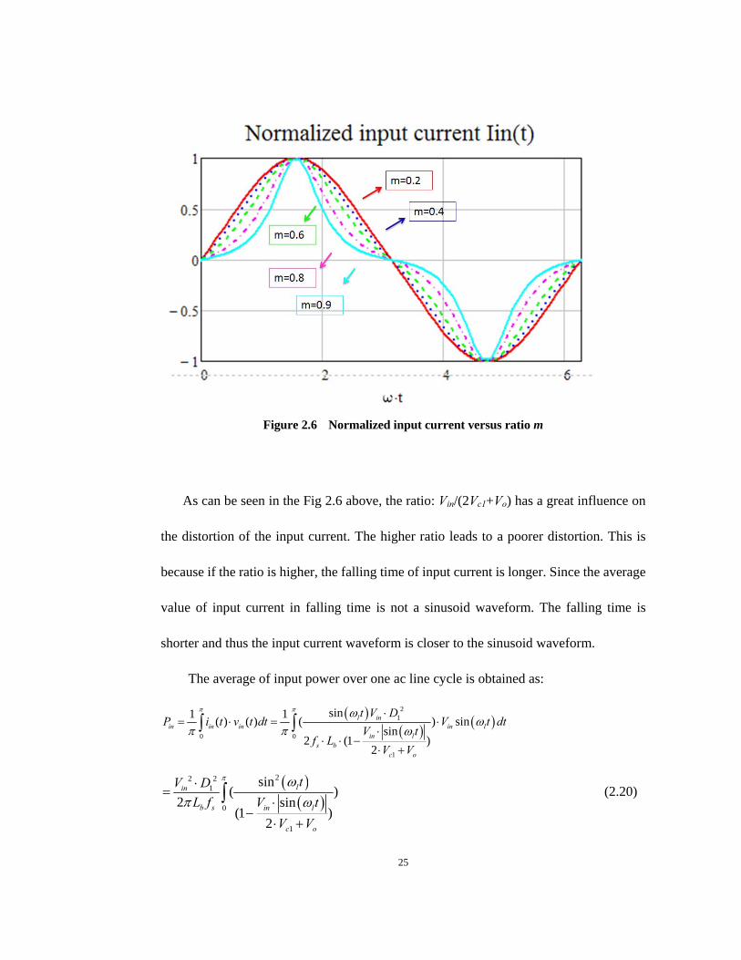
As can be seen in the equation above, the power factor is a function of the ratio:
(2Vc1+Vo)/Vin. The power factor function is plotted in Fig 2.7. The result shows that a
lower ratio leads to a better power factor. Therefore, for the same input voltage and output
voltage, the power factor is determined by the average middle capacitor voltage Vc1, by
neglecting the voltage ripple across the middle capacitor.
Figure 2.7 The power factor as a function of Vin/(2Vc1+Vo)
Assuming the efficiency of the converter is . So:
in oP P (2.22)
27
According to the equ(2.22), the duty cycle D1 can be calculated as:
1 2
0
1
1 2
sin
sin1
2
o b s
in
in
c o
P L fD
V t
V t
V V
(2.23)
According to the charge balance of middle capacitor C1:
2 _1 1_ 2
1 1
2 2 2L pk
s L pk s
iD T i D T
(2.24)
Where
12 _ 1
2
sL pk c
D Ti V
L
(2.25)
11_
1
sin sL pk in l
D Ti V t
L
(2.26)
Therefore,
1
112
1 21
1 1sin
2 2 2
sc
ss in l s
D TV
D TLD T V t D T
L
1 12
1 22 sinc
in
V DL
L V t D
(2.27)
According to equ(2.13),
1 122 2
1
(2 sin )
2 sinc c o in l
in
V V V V tL
L V t
(2.28)
Average equ(2.28) over the ac line period, (2.29) can be derived.
12 12 2
1 0
(2 sin )
2 sinc o in lc
in l
V V V tL Vd t
L V t
(2.29)
From this equation, three conclusions could be made:

28
1) The ratio of L2/L1 is independent of the duty cycle D1
2) The higher the ratio of L2/L1, the larger the middle capacitor voltage Vc1.
3) The voltage across the middle capacitor C1 and C2 is independent of load.
Assuming the power factor is unity, the desired instantaneous load power is not
equal to the desired instantaneous input power. Therefore, some elements within the
system must supply or consume the difference between the instantaneous input power
and output power. In this proposed converter, the middle decoupling valley-fill capacitors
C1 and C2 works as a low-frequency energy storage element. The difference between the
instantaneous input power and instantaneous output power flows through the capacitors.
When the instantaneous input power is larger than instantaneous output power, the
energy flows into the capacitors, and voltage of the capacitors increase. Likewise, when
the instantaneous input power is lower than instantaneous output power, the energy is
released by the capacitors, and voltage of the capacitors decrease, as shown in Fig 2.8.
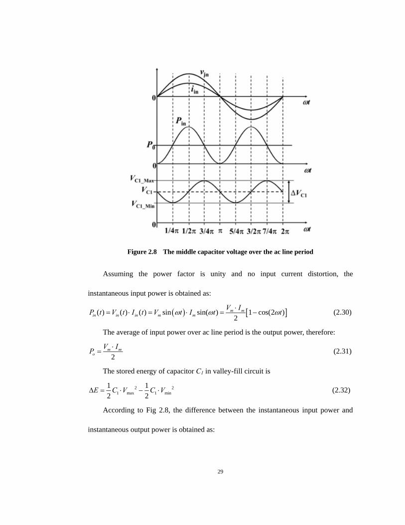
29
Figure 2.8 The middle capacitor voltage over the ac line period
Assuming the power factor is unity and no input current distortion, the
instantaneous input power is obtained as:
( ) ( ) ( ) sin sin( ) 1 cos(2 )2
m min in in m m
V IP t V t I t V t I t t
(2.30)
The average of input power over ac line period is the output power, therefore:
2m m
o
V IP
(2.31)
The stored energy of capacitor C1 in valley-fill circuit is
2 21 max 1 min
1 1
2 2E C V C V (2.32)
According to Fig 2.8, the difference between the instantaneous input power and
instantaneous output power is obtained as:
30
3
4
1
4
oac
line
PE P t dt
(2.33)
Thus the energy stored in each capacitor in valley-fill circuit is obtained as:
3
4
1 21
4
1
2 2o
c c acline
PE E P t dt
(2.34)
According to equ(2.32),(2.34):
2 21 max 1 min
1 1
2 2 2o
line
PC V C V
(2.35)
The low frequency voltage ripple of Vc1 and Vc2 can be derived:
12o
line o
PV
V C
(2.36)
Therefore, the voltage ripple of the middle capacitor is determined by the average
voltage and capacitance of the middle capacitor, for the same output power.
In the typical PFC, since usually the output capacitor takes the responsibility of
low-frequency energy storage, the capacitance need be large so that the low- frequency
ripple of output voltage is as low as possible, especially for LED application. In LED
application, a small output voltage variation could lead to large output current variation.
However, for the proposed SEPIC converter, it is unnecessary that the output
capacitance is large because DCM operation makes the middle valley-fill capacitors
work as low frequency energy storage capacitors rather than the output capacitor, thus
minimizing the need for the low-frequency capacitance since the voltage ripple of
middle valley-fill capacitors could be large. Therefore, by working at DCM and

31
allowing a relative large voltage ripple across the middle capacitors in valley-fill circuit,
it can eliminate the electrolytic capacitors in the proposed converter while maintaining
high power factor and good output regulation.
2.3.2 The Voltage and Current Stress of the devices and components.
According to the operating principle discussed above, the maximum voltage stress
for the MOSFET Q1 can be estimated as:
1_ max 1_ max 2 _ max 1_ max2q c c o c oV V V V V V (2.37)
Vc1_max and Vc2_max is the maximum voltage of middle capacitor C1 and C2.
Since some parasitic ringing may be observed during MOSEFT turn-off transient,
20%-30% margin for voltage stress need be considered for the selection of the
MOSFET Q1.
The maximum voltage stress for the output diode Do is
_ max 1_ max 2 _ maxdo c o c oV V V V V (2.38)
Since the maximum current of inductor L1 and L2 happens at the peak voltage of
maximum input line, the maximum current stress for MOSFET Q1 is obtained as:
_ min 1_ max_ min
1_ max 1_ max 2 _ max1 2
HL PK s c HL s
Q L L
V D T V D TI I I
L L
(2.39)
IL1_max is the maximum current of inductor L1, and IL2_max is the maximum current of
inductor L2. VHL_PK is the peak voltage of maximum input line, Dmin is the duty cycle
under the peak voltage of maximum input line condition. Vc1_max_HL refers to the middle
capacitor voltage under this condition.

32
The current stress for the output diode Do is obtained as:
_ min 1_ max min
_ max 1_ max 2 _ max1 2
HL PK s c s
Do L L
V D T V D TI I I
L L
(2.40)
Therefore, both Q1 and Do carry the sum of the maximum current of inductor L1
and L2. The maximum current of inductor L1 and L2 happens at the peak voltage of high
input line. Therefore, the selection for the output diode should be based on this
equation.
According to the operation principle of the proposed converter, the voltage stress
of the diodes D1-D3 in the valley fill circuit is Vc1_max. The current stress for diode D2 is
the peak current of inductor L1. The current stress for diodes D1 and D3 is the one half of
peak current of inductor L2.
The voltage stress for the middle capacitor C1 and C2 can be calculated in equ(2.29)
under the peak of maximum input voltage.
The valley-fill circuit could reduce the voltage stress of output diode and middle
capacitor under the same power factor condition, thus achieving higher efficiency.
2.4 Experimental Results
A 60W prototype has been built in the Lab and tested to verify the design. The operating
conditions are:
Input Voltage Vin: 130V
Line Frequency: 60Hz
Output Voltage: 50V

33
Switching Frequency(fsw): 60kHz
Maximum Output Power(Po): 60W
The main circuit component values and parameters are given according to the design
equations above, and given in Table 2.1.
Table 2.1 Summary of selected components.
Inductor L1 L1: 180uH PQ3220 Core
Inductor L2 L2: 120uH,PQ3220 Core
MOSFET STB12NM60N, 600V,10A.
Output Diode Schottky, PDS4150 150V,4A
Rectifier Diode Bridge S3G, 400V, 3A
Diodes in Valley-fill Circuit Schottky, SS28,80V,2A
Capacitors in Valley-fill Cap 16uF,300V Film Polyester
Output Capacitor Cap 15uF,63V,Metal Polyester
Controller UCC3844
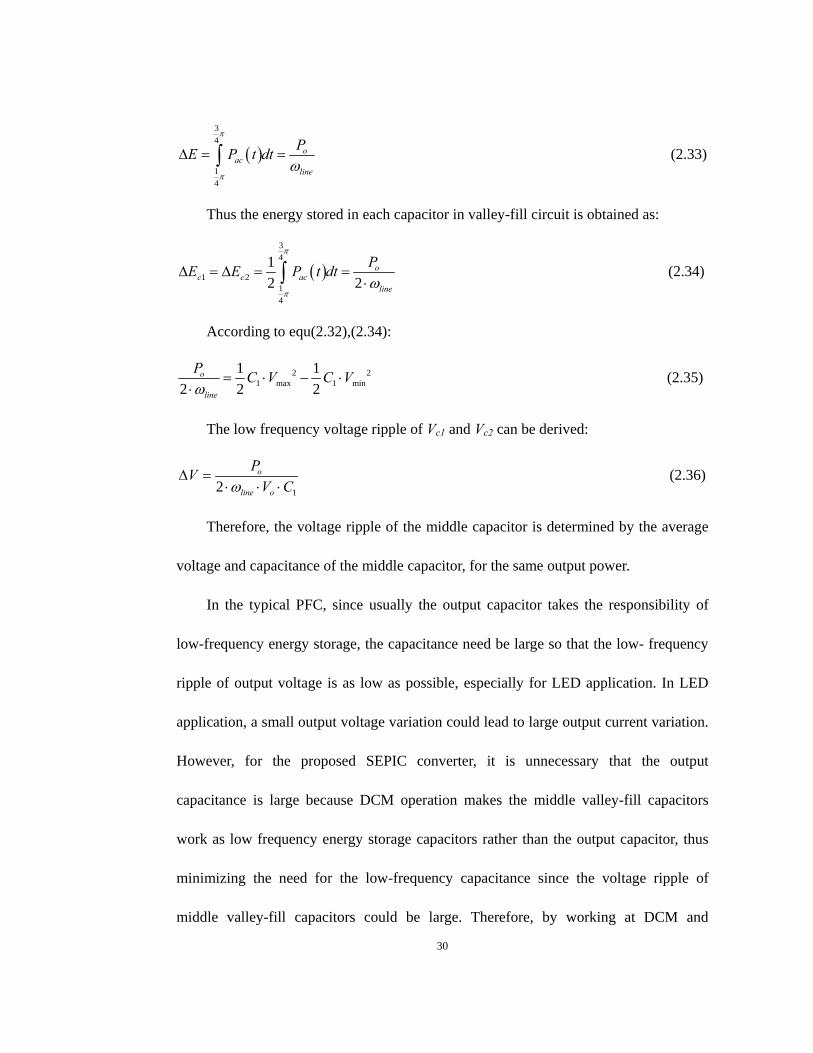
Some of the key waveforms at 100% load are shown in Fig2.9-Fig2.12. It can be seen
that the input current follows the input voltage. The input current distortion is very
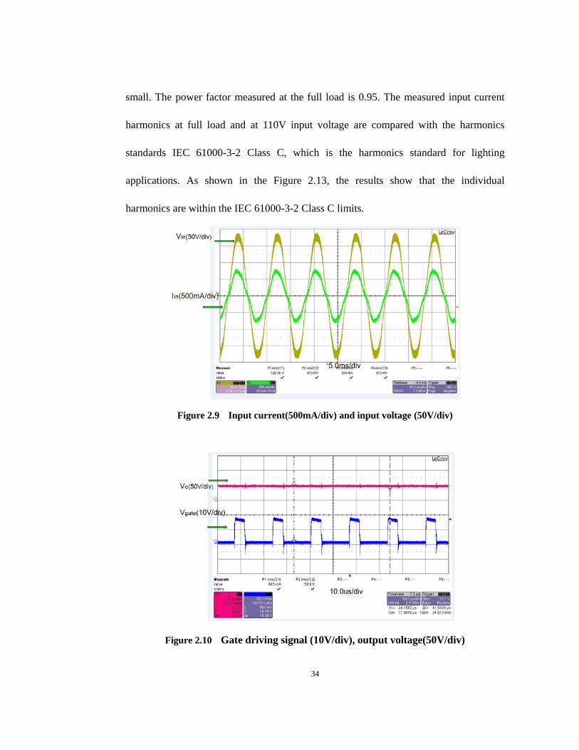
34
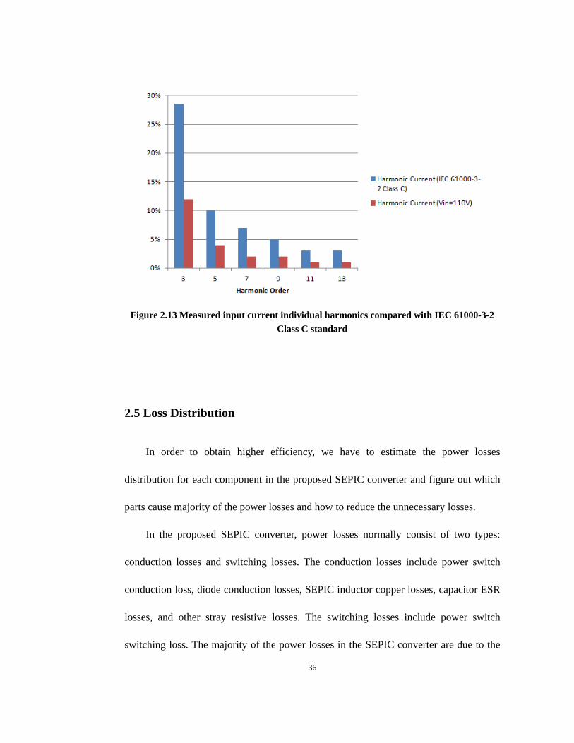
small. The power factor measured at the full load is 0.95. The measured input current
harmonics at full load and at 110V input voltage are compared with the harmonics
standards IEC 61000-3-2 Class C, which is the harmonics standard for lighting
applications. As shown in the Figure 2.13, the results show that the individual
harmonics are within the IEC 61000-3-2 Class C limits.
Figure 2.9 Input current(500mA/div) and input voltage (50V/div)
Figure 2.10 Gate driving signal (10V/div), output voltage(50V/div)
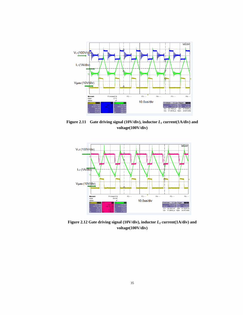
35
Figure 2.11 Gate driving signal (10V/div), inductor L1 current(1A/div) and
voltage(100V/div)
Figure 2.12 Gate driving signal (10V/div), inductor L2 current(1A/div) and
voltage(100V/div)
36
Figure 2.13 Measured input current individual harmonics compared with IEC 61000-3-2
Class C standard
2.5 Loss Distribution
In order to obtain higher efficiency, we have to estimate the power losses
distribution for each component in the proposed SEPIC converter and figure out which
parts cause majority of the power losses and how to reduce the unnecessary losses.
In the proposed SEPIC converter, power losses normally consist of two types:
conduction losses and switching losses. The conduction losses include power switch
conduction loss, diode conduction losses, SEPIC inductor copper losses, capacitor ESR
losses, and other stray resistive losses. The switching losses include power switch
switching loss. The majority of the power losses in the SEPIC converter are due to the
37
losses in inductors and MOSFET.
2.5.1 Inductor Losses
The power losses of inductor L1 and L2 include core loss and copper loss. Magnetic
materials exhibit core loss, due to the low frequency hysteresis of the B-H loop and to
the induced high frequency eddy currents flowing in the core material. The physics of
core loss is extremely complex. No one has yet produced an analysis that allows us to
predict core loss from material structure and chemical makeup. All core loss data is
strictly empirical. There is an Empirical equation for core loss calculation. Constant
coefficients are assigned to a, c, d. It is just curve fitting to the empirical data.
_
c d
fe density swP a f B (2.41)
Where fsw is kHz and the flux density ∆B is in Tesla, a, c, d are curve fitting
parameters that depend on the type of the core material. Over a small range of
frequencies, this empirical equation works reasonably well.
Therefore, the total core loss is obtained:
_fe fe density eP P V (2.42)
Ve is the volumn of the magnetic core.
The copper losses of the inductors include the DC copper loss and high frequency
proximity effect caused loss. To eliminate the proximity losses, Litz wire is used in the
inductors. Many strands of small gauge insulted copper wire are bundle together, and
are externally connected in parallel. To be effective, the diameter of the strands should

38
be sufficiently less than one skin depth.
Therefore, the DC copper losses for the inductor are:
2cu rmsP I R (2.43)
2.5.2 MOSFET Losses
The power loss in any MOSFET is the combination of the switching losses and the
MOSFET’s conduction losses:
MOSFET SW CONDP P P (2.44)
The calculation of conduction loss is straightforward as specified in equ(2.45)
below:
2
_rms
COND ds ds onP I R (2.45)
Where Rds_on is the conduction resistance at the maximum operating MOSFET
junction temperature, and Ids_rms is RMS current of MOSFET.
For discontinuous conduction mode (DCM), there is no reverse recovery issue no
matter what kinds of output diodes are used, thus no reverse recovery loss in the
MOSFET caused by the diodes. The total switching losses for MOSFET is obtained as:
_ _ _
1 1
2 2SW TURNON on ds ds on sw off ds ds off swP T V I f T V I f (2.46)
Where Ton is the turn on time in one switching period, Ids_on is the MOSFET current
at the moment of its turn-on, Toff is the turn off time in one switching period, Ids_off is the
MOSFET current at the moment of its turn-off. Vds is the drain to source voltage of
MOSFET, and fsw is the switching frequency.
39
2.5.3 Diode Losses
The rectifier diode forward voltage drop is a dominant factor determining the
power supply efficiency. The condition loss of the diode is average current of diode
times the forward voltage drop of the diode. Therefore, the conduction losses of the
diodes in valley-fill circuit can be calculated. Since the average current of the output
capacitor is zero. Therefore, the average current of the output diode is the output
current.
COND F oP V I (2.47)
Where VF is the forward voltage of the output diode.
Since the input is the AC line, conduction losses occur in the input bridge rectifier
diodes. The total power loss in the input bridge rectifier is obtained as:
_ _ _4input rectifier F rectifier av rectifierP V I (2.48)
Where VF_rectifier is the forward voltage drop of each input diode in the diode bridge
rectifier and Iavg_rectifier is the average forward current for each diode in the bridge
rectifier.
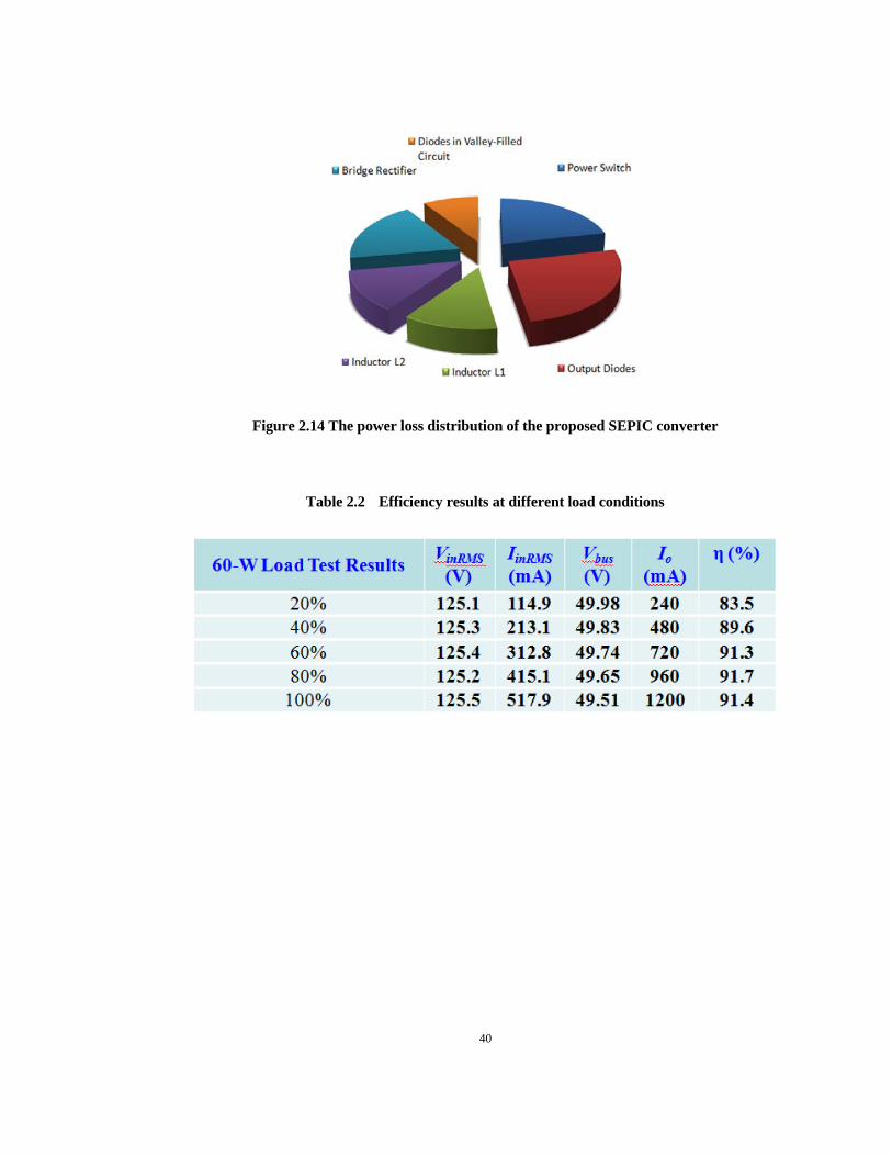
After the power loss calculations, the power loss distribution is given in Fig.2.14.
The efficiency results at different load conditions are given in Table.2.2. Plot these
efficiency data and efficiency with different load curve is obtained as shown in Fig 2.15.
40
Figure 2.14 The power loss distribution of the proposed SEPIC converter
Table 2.2 Efficiency results at different load conditions
41
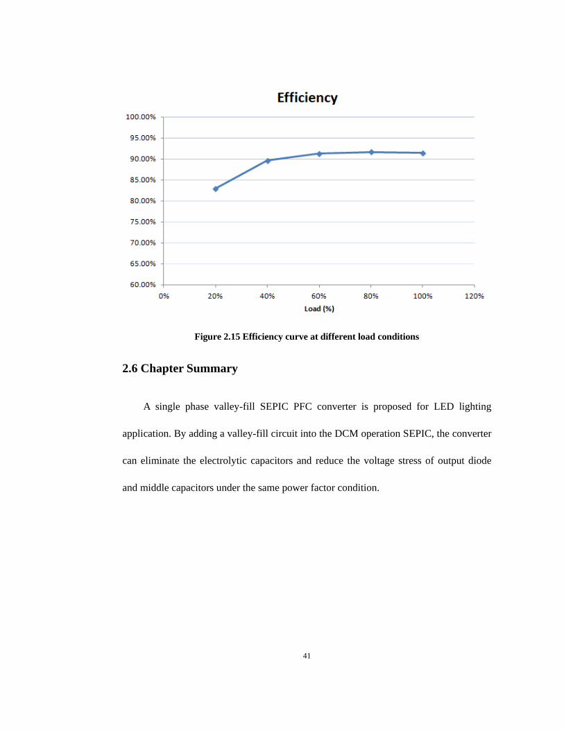
Figure 2.15 Efficiency curve at different load conditions
2.6 Chapter Summary
A single phase valley-fill SEPIC PFC converter is proposed for LED lighting
application. By adding a valley-fill circuit into the DCM operation SEPIC, the converter
can eliminate the electrolytic capacitors and reduce the voltage stress of output diode
and middle capacitors under the same power factor condition.
42
CHAPTER 3
INTERLEAVED SEPIC WITH VALLEY FILLED CIRCUIT
FOR LED APPLICATION
3.1 Introduction of interleaving technique
Interleaving technology has been applied to many applications in the field of
power electronics, especially in high power applications. Since in high power
application, the voltage and current stress of the device can go beyond the limit so that
the power device cannot handle. In this case, paralleling the devices can provide the
solution, but one major concern of this solution is the current sharing and voltage
sharing. There is another solution, which is paralleling the converters instead of power
devices. By paralleling the converters and making each channel a phase shift, the
interleaved converter can be proposed and some beneficial features such as ripple
cancellation and better thermal performance can be achieved.
In lower power level, such as SMPS power stage architecture, the interleaving
technique can also be applied. In such applications, some concerns have been listed
below
1. The ESRs of the input and output filter capacitors cause large heat dissipation
from the high switching pulsed current. Interleaving multiple converters can

43
significantly reduce the ripple current of the input capacitors and output
capacitors so that reduce the thermal stress of the capacitors.
2. N-channel interleaved converter increases the ripple frequency to be n times the
individual switching frequency. Since the ESR of the tantalum capacitors is
inversely proportional to the frequency. Therefore, interleaving technique can
effectively reduce the filter capacitor size and weight.
3. In the case that higher power levels are required than the initial design at the
beginning. Higher power levels can be achieved with interleaved converter by
adding additional identical modules.
Therefore, the interleaving technique has been investigated and applied to many
applications. The multi-phase/interleaved buck converter for Voltage Regulator (VR)
application has been mostly investigated and explored [63-65].
3.2 Review of Multi-Phase Buck for VR Application
A Voltage Regulator Module (VRM) is a buck converter that can provide the CPU
supply voltage, which converts +5V or +12V to a lower voltage required by CPU.
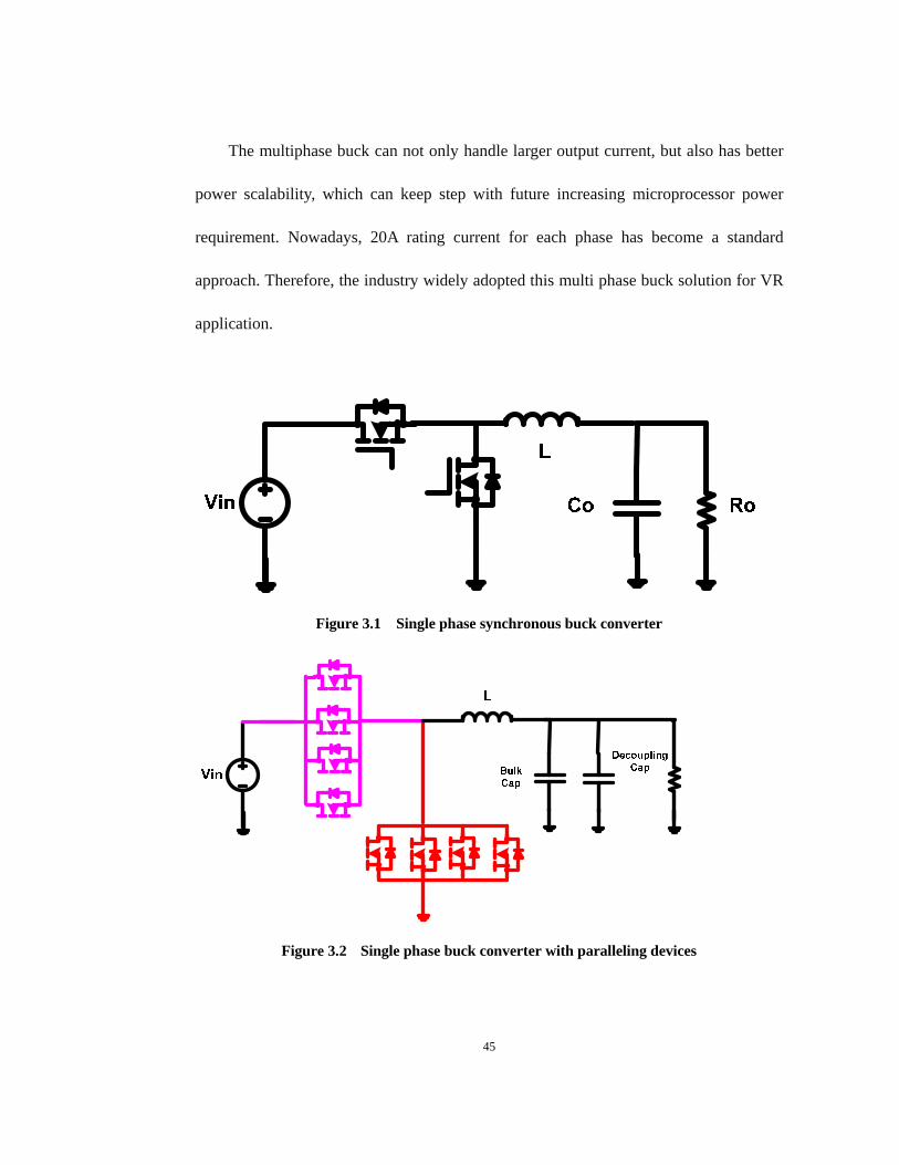
For the older generation microprocessor VR, the single phase synchronous buck
topology is widely adopted, as shown in Fig3.1 [63]. However, although the output
voltage of the VR tends to drop, the output current increases a lot so that the total power
consumptions of CPU increase continuously. It is impossible for a single buck converter
to handle such large current stress and power consumption. Naturally the devices are
44
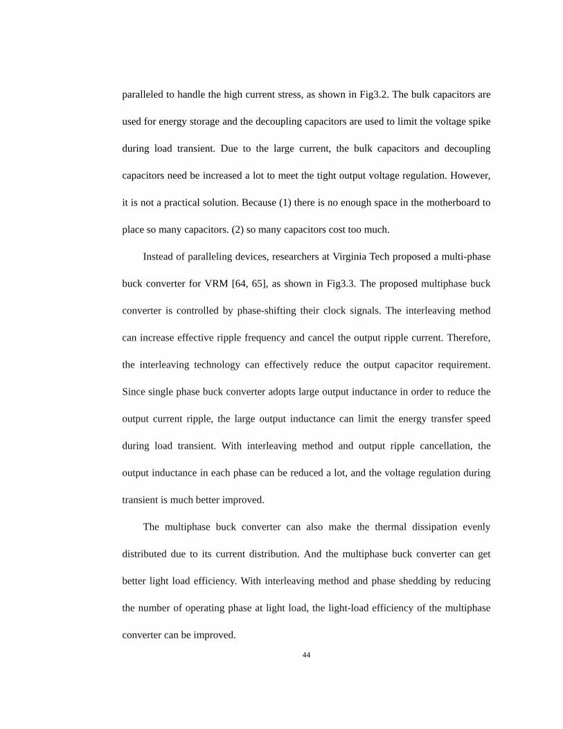
paralleled to handle the high current stress, as shown in Fig3.2. The bulk capacitors are
used for energy storage and the decoupling capacitors are used to limit the voltage spike
during load transient. Due to the large current, the bulk capacitors and decoupling
capacitors need be increased a lot to meet the tight output voltage regulation. However,
it is not a practical solution. Because (1) there is no enough space in the motherboard to
place so many capacitors. (2) so many capacitors cost too much.
Instead of paralleling devices, researchers at Virginia Tech proposed a multi-phase
buck converter for VRM [64, 65], as shown in Fig3.3. The proposed multiphase buck
converter is controlled by phase-shifting their clock signals. The interleaving method
can increase effective ripple frequency and cancel the output ripple current. Therefore,
the interleaving technology can effectively reduce the output capacitor requirement.
Since single phase buck converter adopts large output inductance in order to reduce the
output current ripple, the large output inductance can limit the energy transfer speed
during load transient. With interleaving method and output ripple cancellation, the
output inductance in each phase can be reduced a lot, and the voltage regulation during
transient is much better improved.
The multiphase buck converter can also make the thermal dissipation evenly
distributed due to its current distribution. And the multiphase buck converter can get
better light load efficiency. With interleaving method and phase shedding by reducing
the number of operating phase at light load, the light-load efficiency of the multiphase
converter can be improved.
45
The multiphase buck can not only handle larger output current, but also has better
power scalability, which can keep step with future increasing microprocessor power
requirement. Nowadays, 20A rating current for each phase has become a standard
approach. Therefore, the industry widely adopted this multi phase buck solution for VR
application.
Figure 3.1 Single phase synchronous buck converter
Figure 3.2 Single phase buck converter with paralleling devices
46
Figure 3.3 The multiphase buck converter with interleaving each phase
3.3 Interleaved SEPIC with valley fill circuit
Interleaving technology has been used in the proposed SEPIC in order to further
reduce the filter size, and gain higher efficiency. The mechanism is that through
interleaving of the converters in parallel with phase shift of each other, some ripple can
be totally cancelled due to the phase shift and the RMS current of output capacitor is
reduced. Therefore, the size of output capacitor and EMI filter can be greatly reduced.
Interleaved SEPIC converter with valley fill circuit is shown in Fig.3.4. The
converter works in peak current mode control and discontinuous current mode so that it
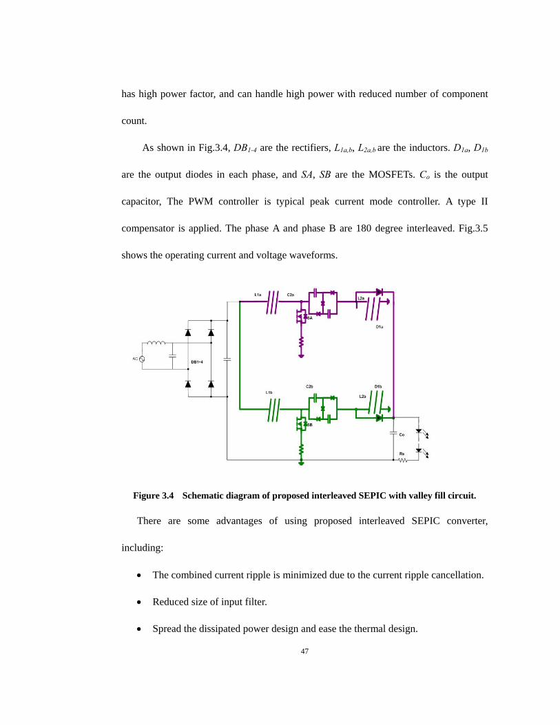
47
has high power factor, and can handle high power with reduced number of component
count.
As shown in Fig.3.4, DB1-4 are the rectifiers, L1a,b, L2a,b are the inductors. D1a, D1b
are the output diodes in each phase, and SA, SB are the MOSFETs. Co is the output
capacitor, The PWM controller is typical peak current mode controller. A type II
compensator is applied. The phase A and phase B are 180 degree interleaved. Fig.3.5
shows the operating current and voltage waveforms.
Figure 3.4 Schematic diagram of proposed interleaved SEPIC with valley fill circuit.
There are some advantages of using proposed interleaved SEPIC converter,
including:
The combined current ripple is minimized due to the current ripple cancellation.
Reduced size of input filter.
Spread the dissipated power design and ease the thermal design.
48
High power factor.
DCM operation of inductor current in SEPIC converter with valley fill circuit to
eliminate the issue of current sharing, and reduce the complexity of controller.
More phases of converters can be interleaved.
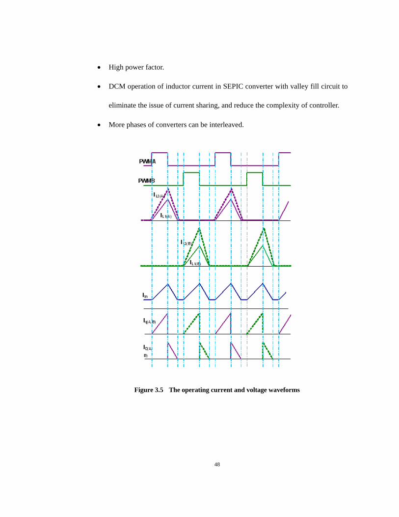
Figure 3.5 The operating current and voltage waveforms

49
3.4 Experimental Results for the proposed interleaved SEPIC with
valley fill circuit
100W prototype has been built in the Lab and tested to verify the design. The
operating conditions are:
Input Voltage Vin: 110V
Line Frequency: 60Hz
Output Voltage: 60V
Switching Frequency(fsw): 70kHz
Maximum Output Power(Po): 100W
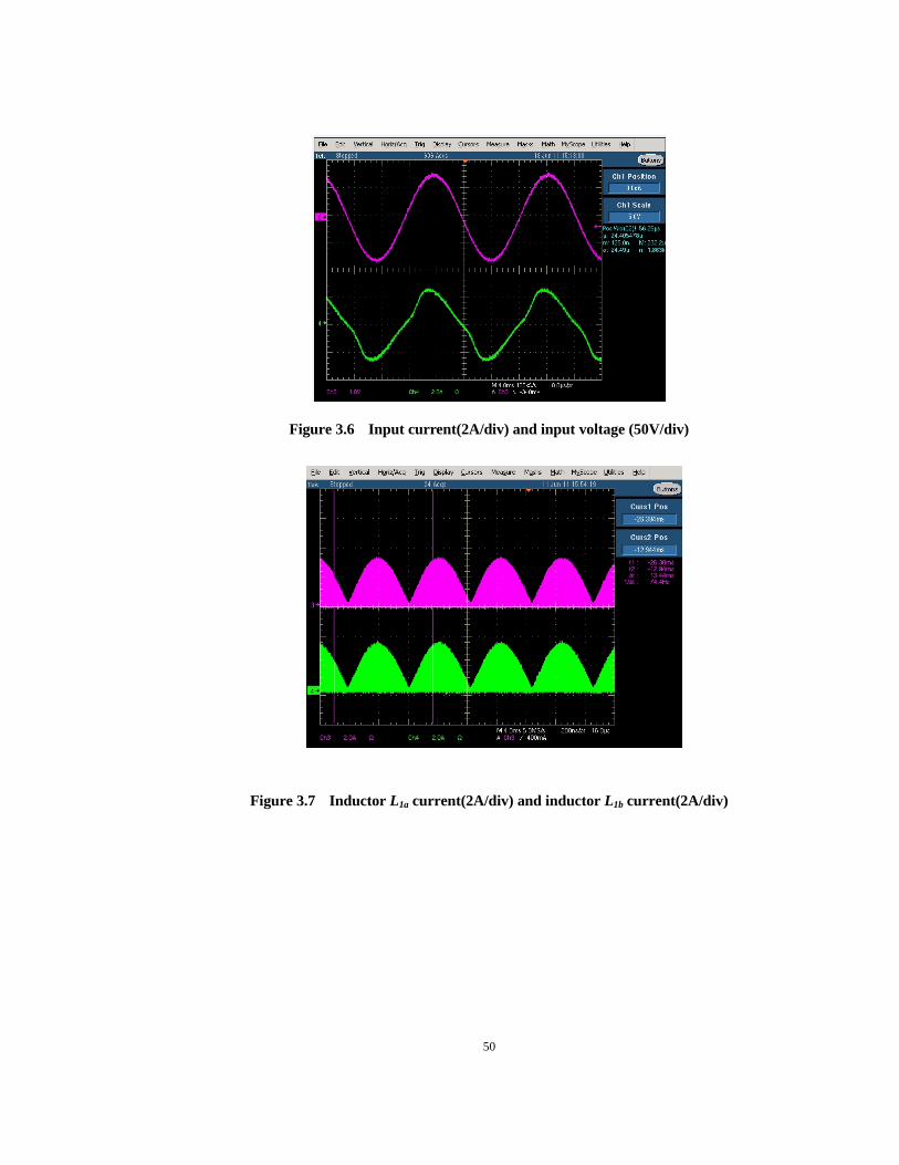
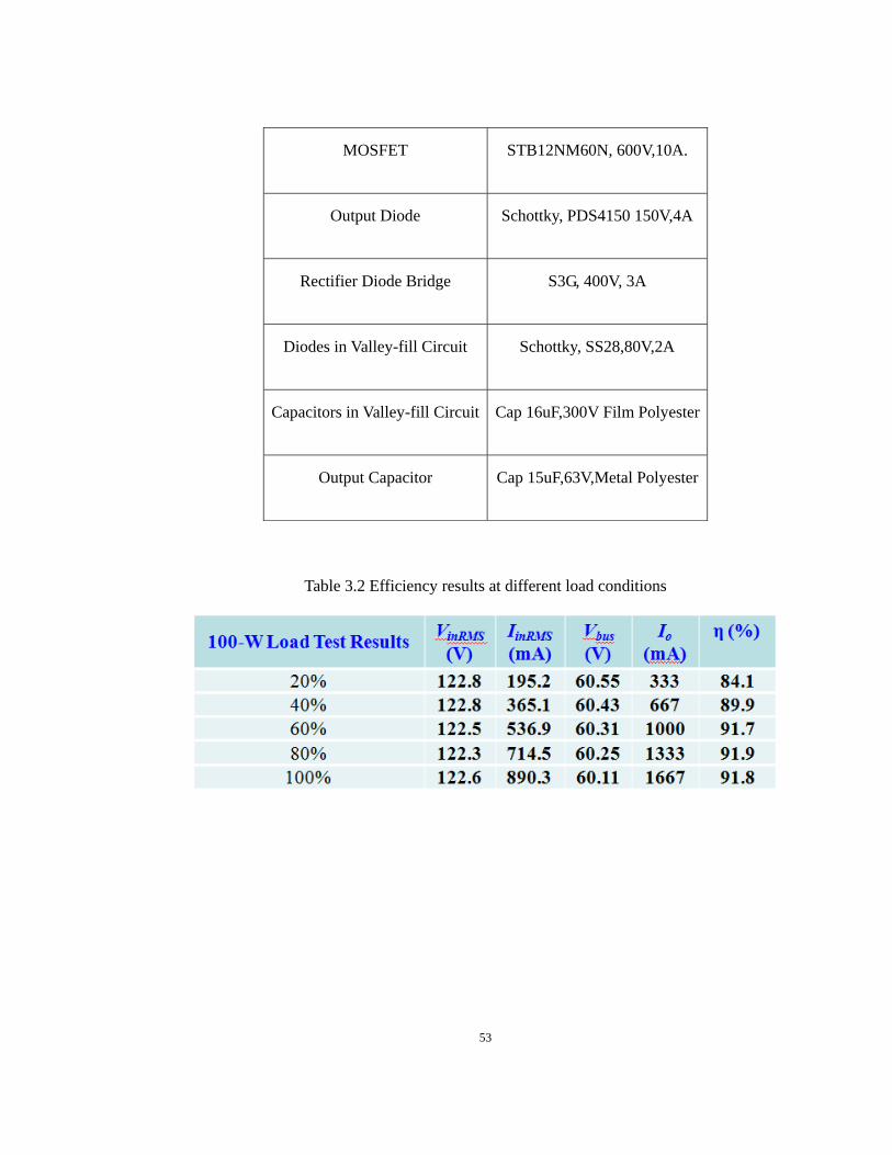
Some of the key waveforms at 100% load are shown in Fig3.6-Fig3.9. It can be seen
that the input current distortion is very small. The power factor measured at 100% load
is 0.96. The measured input current harmonics at full load and at 110V input voltage are
compared with the harmonics standards IEC 61000-3-2 Class C, which is the harmonics
standard for lighting applications. As shown in the Figure 3.10, the results show that the
individual harmonics are within the IEC 61000-3-2 Class C limits. The results are
almost the same as the proposed single phase Modified SEPIC.
50
Figure 3.6 Input current(2A/div) and input voltage (50V/div)
Figure 3.7 Inductor L1a current(2A/div) and inductor L1b current(2A/div)
51
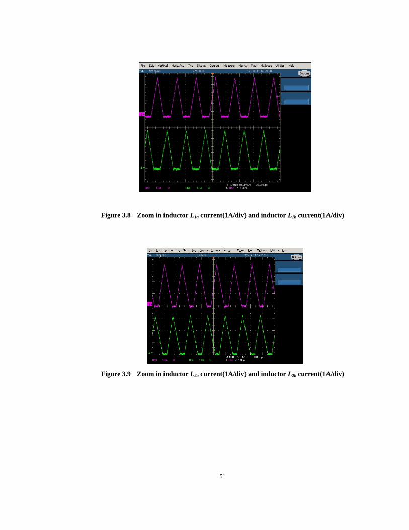
Figure 3.8 Zoom in inductor L1a current(1A/div) and inductor L1b current(1A/div)
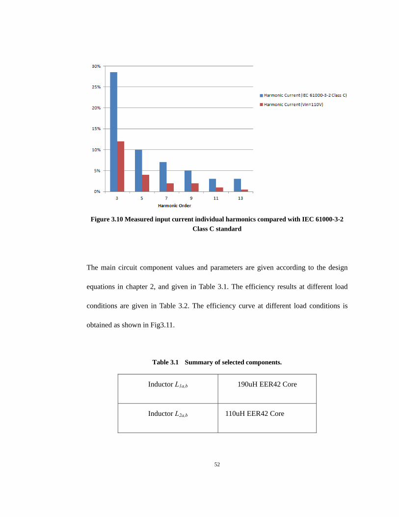
Figure 3.9 Zoom in inductor L2a current(1A/div) and inductor L2b current(1A/div)
52
Figure 3.10 Measured input current individual harmonics compared with IEC 61000-3-2
Class C standard
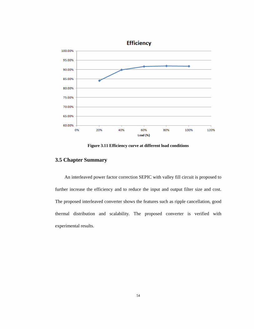
The main circuit component values and parameters are given according to the design
equations in chapter 2, and given in Table 3.1. The efficiency results at different load
conditions are given in Table 3.2. The efficiency curve at different load conditions is
obtained as shown in Fig3.11.
Table 3.1 Summary of selected components.
Inductor L1a,b 190uH EER42 Core
Inductor L2a,b 110uH EER42 Core
53
MOSFET STB12NM60N, 600V,10A.
Output Diode Schottky, PDS4150 150V,4A
Rectifier Diode Bridge S3G, 400V, 3A
Diodes in Valley-fill Circuit Schottky, SS28,80V,2A
Capacitors in Valley-fill Circuit Cap 16uF,300V Film Polyester
Output Capacitor Cap 15uF,63V,Metal Polyester
Table 3.2 Efficiency results at different load conditions
54
Figure 3.11 Efficiency curve at different load conditions
3.5 Chapter Summary
An interleaved power factor correction SEPIC with valley fill circuit is proposed to
further increase the efficiency and to reduce the input and output filter size and cost.
The proposed interleaved converter shows the features such as ripple cancellation, good
thermal distribution and scalability. The proposed converter is verified with
experimental results.
55
CHAPTER 4
CONCLUSIONS AND SUGGESTIONS FOR FUTURE
RESEARCH
4.1 Conclusions
This thesis describes an investigation into the light emitting diode (LED) lamp
driven by electronic ballast. The comprehensive overview on the lighting development
is given. The characteristic of the light emitting diode (LED) lamp is described. The
requirements of the ballast for the light emitting diode (LED) lamp are presented.
A single phase, power factor correction converter without electrolytic capacitors
for LED lighting applications is proposed, which is a modified SEPIC converter
working in discontinuous conduction mode (DCM). Different with a conventional
SEPIC converter, the middle capacitor is replaced with a valley-fill circuit. The
principle of the theory is derived. The valley-fill circuit could reduce the voltage stress
of output diode and middle capacitor under the same power factor condition, thus
achieving higher efficiency. The proposed converter is verified with experimental
results.
An interleaved power factor correction SEPIC with valley fill circuit is proposed to
further increase the efficiency and to reduce the input and output filter size and cost.
The proposed interleaved converter shows the features such as ripple cancellation, good
thermal distribution and scalability. The proposed converter is verified with

56
experimental results.
4.2 Contributions and Suggestions for Future Work
The contributions of the author include:
Design and implement a single phase, power factor correction converter
without electrolytic capacitors for LED lighting applications, which is a
modified SEPIC converter working in discontinuous conduction mode
(DCM).
Propose and implement an interleaved power factor correction SEPIC with
valley fill circuit to further increase the efficiency and reduce the input and
output filter size and cost.
Compared with discontinuous conduction mode, interleaved critical conduction
mode PFC, which is based variable frequency modulation, can add some advantages
including lower peak current and better thermal management to gain better efficiency. In
addition, it also has smaller differential mode EMI filter than a single stage converter
with the same total power rating. Hence how to design a critical conduction mode
control for the proposed Modified SEPIC converter is a good topic for future work. And
how to design the coupled inductors between the interleaved converters working in
variable-frequency will be also a good topic for future work.

57
REFERENCE
[1] D. C. Pritchard. lighting. Addison Wesley Longman Limited, Sixth Edition, 1999.
[2] B. Cook. “New developments and future trends in high-efficiency lighting”.
Engineering Science and Education Journal, vol9, no5. Oct. 2000:207-17.
[3] G. Zissis. “Electrical light sources: a challenge for the future”. Engineering Science
and Education Journal, vol9, no5. Oct. 2000:194 –5.
[4] J. Lindsey, Applied Illumination Engineering, Fairmont Press, Inc.,1991.
[5] I. P. Raizer. Gas Discharge Physics, Berlin: Springer-Verlag, 1991.
[6] J. Waymouth. "Electric Discharge Lamps". MIT press, 1972.
[7] J. P. Frier, M. E. G. Frier. Industrial Lighting Systems. McGraw-Hill, Inc, 1980.
[8] K. Chen. Energy Effective Industrial Illuminating Systems, . The Fairmont Press,
Inc,1994.
[9] Y. K. Cheng, K. W. E. Cheng. “General study for using LED to replace traditional
lighting devices”. in Proc International Conference on Power Electronics Systems and
Applications,. Nov. 2006:173 – 7.
[10] B. Heffernan, L. Frater, N. Watson. "LED replacement for fluorescent tube
lighting". in Australasian Universities Power Engineering Conference, AUPEC'07.
Dec. 2007:1-6.
[11] M. O. Holcomb, R. M. Mach, G. O. Mueller, D. Collins, R. M. Fletcher, D. A.
Steigerwald, et al. "The LED lightbulb: are we there yet? progress and challenges for

58
solid state illumination". In Conference on Lasers and Electro-Optics, CLEO '03. Jun.
2003:4-5.
[12] Fluorescent lamp, from Wikipedia.
[13] H. S. H. Chung, N. W. Ho, W. Yan, P. Tam, S. Y. R. Hui. “Comparison of dimmable
electromagnetic and electronic ballast systems—an assessment on energy efficiency and
lifetime”. IEEE Transaction on Industry Electronics, vol 54, no 6. Dec. 2007:3145 –
54.
[14] Light emitting diode, from Wikipedia.
[15] E. F. Schubert, “Light-emitting diodes”, Chapter 5, 2nd Edition, Cambridge, 2006.
[16] Luxeon Power Light Source, Data Sheet DS51, LUEXON POWER LEDS.
http://www.lumileds.com/pdfs/DS51.pdf.
[17] A. J. Calleja, M. Ricosecades, J. Cardesin, J. Ribas, E. L. Corominas. “Evaluation
of a high efficiency boost stage to supply a permanent LED emergency lighting system”.
in Proc Industry Electronics Society Annual Meeting, IECON'04. Nov. 2004:1390-5.
[18] J. Bielecki, A. S. Jwania, E. Khatib, T. Poorman. “Thermal considerations for LED
components in an automotive lamp”. in Twenty Third Annual IEEE Semiconductor
Thermal Measurement and Management Symposium, SEMI-THERM’07. Mar.
2007:37-43.
[19] Lai Y, Cordero N, Barthel F, Tebbe F, Kuhn J, Apfelbeck R, et al. Liquid cooling of
bright LEDs for automotive applications. Applied Thermal Engineering.
2009;29(5-6):1239-44.

59
[20] M. Rico-Secades, A. J. Calleja, J. Cardesin, J. Ribas, E. L. Corominas, J. M.
Alonso, et al. "Driver for high efficiency LED based on flyback stage with current mode
control for emergency lighting system". in IEEE industry Applications Society Annual
Conference, IAS'04. Oct. 2004:1655 - 9.
[21] C. C. Chen, C. Y. Wu, Y.M. Chen, T. F. Wu. “Sequential Color LED Backlight
Driving System for LCD Panels”. IEEE Transactions on Power Electronics. p. 919 –
25.
[22] C. L. Chiu, K. H. Chen. “A high accuracy current-balanced control technique for
LED backlight”. in IEEE Power Electronics Specialists Conference, PESC'08. Jun.
2008:4202 – 6,.
[23] S. Y. Lee, J. W. Kwon, H. S. Kim, M. S. Choi, K. S. Byun. "New Design and
Application of High Efficiency LED Driving System for RGB-LED Backlight in LCD
Display". in IEEE Power Electronics Specialists Conference, PESC'06. Jun.
2006:1-5.
[24] I. H. Oh. “a single-stage power converter for a large screen LCD back-lighting”. in
IEEE Applied Power Electronics Conference, APEC'06. Mar. 2006: pp.1058-63.
[25] S. Y. Tseng, S. C. Lin, H. C. Lin. "LED backlight power system with auto-tuning
regulation voltage for LCD panels". in IEEE APplied Power Electronics Conference,
APEC'08. Feb. 2008:551-7.
[26] H. J. Chiu, S. J. Cheng. "LED Backlight Driving System for Large-Scale LCD
Panels". IEEE Transactions on Industrial Electronics, vol 54, no 5. Oct. 2007:2751 –
60
60.
[27] L. Trevisanello, M. Meneghini, G. Mura, M. Vanzi, M. Pavesi, G. Meneghesso, et al.
“Accelerated life test of high brightness light emitting diodes”. IEEE Transactions on
Device and Materials Reliability, vol 8, no 2. Jun. 2008:304-11.
[28] Z. Ye, F. Greenfeld, Z. Liang. “Design Considerations of a High Power Factor
SEPIC Converter for High Brightness White LED Lighting Applications”. in IEEE
Power Electronics Specialists Conference, PESC’08. Jun. 2008:2657-63.
[29] K. I. Hwu, Y. T. Yau, L. L. Lee. 'Powering LED Using High-Efficiency SR Flyback
Converter” in IEEE Applied Power Electronics Conference, APEC'09. Feb.
2009:563-9.
[30]“Datasheet of Luxeon Emitter”, LUEXON POWER LEDS.
http://www.lumileds.com/pdfs/DS51.pdf
[31] Z. Ye, F. Greenfeld, Z. Liang. “A topology study of single-phase offline AC/DC
converters for high brightness white LED lighting with power factor pre-regulation and
brightness dimmable". in Annual Conference of Industrial Electronics, IECON'08.
Nov. 2008:1961 - 7
[32] Rand, B. Lehman, A. Shteynberg. "Issues, Models and Solutions for Triac
Modulated Phase Dimming of LED Lamps". in IEEE Power Electronics Specialists
Conference, PESC'07. Jun. 2007:1398 – 404.
[33] F. Bernitz, O. Schallmoser, W. Sowa. "Advanced Electronic Driver for Power
LEDs with Integrated Colour Management". in IEEE Industry Applications Society
61
Annual Conference, IAS'06. Oct. 2006:2604-7.
[34] A.I. Pressman. “Switching power supply design - Chapter 16: High-frequency
power sources for fluorescent lamps” 2nd McGraw-Hill International Edition,.575.
[35] N. Prathyusha, D.S. Zinger. “An effective LED dimming approach”. in IEEE
Industry Applications Society Annual Conference, IAS'04. Oct. 2004:1671 - 6.
[36] X. R. Xu. "High dimming ratio LED driver with fast transient boost converter". in
IEEE Power Electronics Specialists Conference, PESC’08. Jun. 2008 4192 – 5.
[37] S. Y. R. Hui, W. Yan. “Re-examination on energy saving & environmental issues in
lighting applications”. in International Symposium on Science & Technology of Light
Sources. May. 2007.
[38] G. Carraro. “Solving high-voltage off-line HB-LED constant-current control-circuit
issues”. in IEEE Applied Power Electronics Conference, APEC'07. Feb. 2007:1316-8.
[39] D. Gacio, J. M. Alonso, A. J. Calleja, J. Garcia, M. Rico. “A Universal-Input
Single-Stage High Power-Factor Power Supply for HB-LEDs Based on Integrated
Buck-Flyback Converter”. in IEEE Applied Power Electronics Conference, APEC'09.
Feb. 2009:571-6.
[40] S. E. Mineiro, F.L.M. Antunes, A. J. Perin. “Low cost self-oscillating ZVS-CV
driver for power LEDs". in IEEE Power Electronics Specialists Conference, PESC'08.
Jun. 2008:4196-201.
[41] V. D. B. Heinz, S. Georg, W. Matthias. "Power driver topologies and control
schemes for LEDs". in IEEE Applied Power Electronics Conference, APEC'07. Feb.
62
2007:1319 - 25.
[42] J. Sebastian, D. G. Lamar, M. Arias, M. Rodriguez, M. M. Hernando. "A very
simple control strategy for power factor correctors driving high-brightness
lighting-emitting diodes". in IEEE Applied Power Electronics Conference, APEC'08.
Feb. 2008:537-43.
[43] IEC 1000-3-2 International Standard, Limits for Harmonic Current Emission First
Edition, 1995-03. .
[44] IEC 61000, Electromagnetic compatibility (EMC) Part 3; Limits for harmonic
current emissions (equipment up to and including 16 A per phase) and Part 4; Testing
and measurement techniques (published by the International Electrotechnical
Commission).
[45] Z. Ye, F. Greenfeld, Z. Liang. “ Offline SEPIC converter to drive the high
brightness white LED for lighting applications". in Annual Conference of Industrial
Electronics, IECON'08. Nov. 2008:1994 - 2000.
[46] H. M. Huang, S. H. Twu, S. J. Cheng, H. J. Chiu. “A Single-Stage SEPIC PFC
Converter for Multiple Lighting LED Lamps”. in 4th IEEE International Symposium on
Electronic Design, DELTA'08. Jan. 2008:15 – 9.
[47] K.N. Zhou, J. G. Zhang, Yuvarajan, S. D. F. Weng. “Quasi-Active Power Factor
Correction Circuit for HB LED Driver”. IEEE Trans Power Electronics, vol23, no3.
Mar.2008:1410-5.
[48] T. F. Pan, H. J. Chiu, S. J. Cheng, S. Y. Chyng. "An Improved Single-Stage
63
Flyback PFC Converter for High-Luminance Lighting LED Lamps". In 8th
International Conference on Electronic Measurement and Instruments, ICEMI '07. Jul.
2007:212-5.
[49] H. Sugiyama, S. Haruyama, M. Nakagawa. "Brightness Control Methods for
Illumination and Visible-Light Communication Systems". in International Conference
on Wireless and Mobile Communications, ICWMC'07. Mar. 2007:78-9.
[50] L. Svilainis. "Considerations of the Driving Electronics of LED Video Display". in
International Conference on Information Technology Interfaces, ITI'07 Jun. 2007:431
- 6.
[51] "LED-driver considerations", Texas Instruments Incorporated.
[52] M. Dyble, N. Narendran, A. Bierman, T. Klein. "Impact of dimming white LEDs:
chromaticity shifts due to different dimming methods". in Fifth International
Conference on Solid State Lighting, SPIE'05. 2005:291-9.
[53] M. Doshi, R. Zane. “Digital Architecture for Driving Large LED Arrays with
Dynamic Bus Voltage Regulation and Phase Shifted PWM”. in IEEE Applied Power
Electronics Conference, APEC'07. Feb. 2007:287 – 93.
[54] M. Doshi, R. Zane. “Reconfigurable and fault tolerant digital phase shifted
modulator for luminance control of LED light sources”. in IEEE Power Electronics
Specialists Conference, PESC'08. Jun. 2008:4185 – 91.
[55] K. H. Lee, Y. J. Woo, H. S. Han, K. C. Lee, C. S. Chae, G. H. Cho. "Power-efficient
series-charge parallel-discharge charge pump circuit for LED drive'. In IEEE Power
64
Electronics Specialists Conference, PESC'08. Jun. 2008:2645 - 9.
[56] “Datasheet of Luxeon Emitter”, LUEXON POWER LEDS.
http://www.lumileds.com/pdfs/DS51.pdf
[57] S. K. Maddula, J. C. Balda. “Lifetime of electrolytic capacitors in regenerative
induction motor drives”. in IEEE Power Electronics Specialists Conference, PESC’05.
Jun. 2005:153-9.
[58] X. H. Qu, S. C. Wong, C. K. Tse, X. B. Ruan. 'Isolated PFC Pre-Regulator for
LED Lamps'. in Annual Conference of Industrial Electronics, IECON'08. Nov.
2008:1980 - 7.
[59] W. H. Chang, H. S. Nien, C. H. Chen. "A Digital boost converter to drive white
LEDs". in IEEE Applied Power Electronics Conference, APEC'08. Feb. 2008:558 -
64.
[60] M. Nishikawa, Y. Ishizuka, H. Matsuo, K. Shigematsu. “An LED drive circuit with
constant-output-current control and constant-luminance control”. in
Telecommunications Energy Conference, INTELEC'06. Sep. 2006:1-6.
[61] J. R. Britto, A. E. Demian, L. C. Freitas, V. J. Farias, E. A. A. Coelho, J. B. Vieira.
“A proposal of Led Lamp Driver for universal input using Cuk converter” in IEEE
Power Electronics Specialists Conference, PESC'08. Jun. 2008:2640 - 4.
[62] Hongbo Ma, Jihsheng Lai, Quanyuan Feng, Wensong Yu, Cong Zheng, Zheng
Zhao, “A Novel Valley-Fill SEPIC-Derived Power Supply Without Electrolytic
Capacitor for LED Lighting Application”. IEEE Transaction on Power Electronics, vol
65
27, no 6. 2012:3057-3071.
[63] Xunwei Zhou, "Low voltage high efficiency fast transient voltage regulator
module", Ph.D Dissertation, Virginia Tech, July 1999.
[64] M. Zhang, M. Jovanovic, F. C. Lee, "Design considerations for low voltage on
board DC/DC modules for next generations of data processing circuits", IEEE
Transactions on Power electronics, March 1996, pp.328-337.
[65] X. Zhou, X. Zhang, J. Liu, P. Wong, J. Chen, H. Wu, L. Amoroso, F. C. Lee, D. Y.
Chen, "Investigation of candidate VRM topology for future microprocessors", in Proc.
IEEE APEC, 1998, pp. 145-150.