Embed Size (px)
Citation preview

Application ReportHigh-Performance CMOS Image Sensor Power Supply in Industrial Camera and Vision
Wenting Wu
ABSTRACTThis application note provides solutions for powering the high-performance CMOS image sensors of industrial machine vision cameras or vision sensors for factory automation and control applications. This application report shows the importance of selecting the right components to generate better power supply rails. Three different solutions are approached, including a discrete solution and two integrated solutions based on different PMICs, which feature:• Specific power sequences• Flexible capabilities for driving large output capacitors• Improved efficiency performances• Small sizes
Table of Contents1 Introduction.............................................................................................................................................................................32 TI Solutions............................................................................................................................................................................. 53 Test Results...........................................................................................................................................................................194 Analysis................................................................................................................................................................................. 245 Summary............................................................................................................................................................................... 266 References............................................................................................................................................................................ 277 Revision History................................................................................................................................................................... 27
List of FiguresFigure 1-1. Specific Power Sequencing Needs........................................................................................................................... 4Figure 2-1. Block Diagram of Discrete Solution Board................................................................................................................ 6Figure 2-2. Block Diagram of PMIC TPS65000 Solution............................................................................................................. 7Figure 2-3. Block Diagram of PMIC TPS650330-Q1 Solution..................................................................................................... 7Figure 2-4. Power Supply Rejection Ration Versus Frequency and Input Voltage......................................................................9Figure 2-5. Power Supply Rejection Ratio Versus Frequency and Output Current..................................................................... 9Figure 2-6. Output Noise Versus Output Voltage.........................................................................................................................9Figure 2-7. Noise Versus Frequency and CFFx.......................................................................................................................... 9Figure 2-8. Load Transient Response Versus Voutx................................................................................................................... 9Figure 2-9. The Block Diagram of TPS62841DLC.....................................................................................................................10Figure 2-10. Efficiency vs Load Current (VOUT=1.8V)..............................................................................................................10Figure 2-11. The Schematic of Discrete Solution.......................................................................................................................13Figure 2-12. PCB Board of Discrete Solution............................................................................................................................ 14Figure 2-13. Block Diagram of the TPS65000........................................................................................................................... 15Figure 2-14. Block Diagram of the TPS650330-Q1................................................................................................................... 17Figure 3-1. Power Sequences of CMOS Image Sensor Power Rails........................................................................................20Figure 3-2. Efficiency of the Digital Rail Supplied by TPS7A90 or TPS62840 in PYTHON 300/500/1300 CMOS Image
Sensors.................................................................................................................................................................................. 21Figure 3-3. Efficiency of the Digital Rail Supplied by TPS7A90 or TPS62841 in IMX25X/26X CMOS Image Sensors.............21Figure 3-4. Power Sequences of the Power Rails of the CMOS Image Sensors Using the TPS65000 Solutions.................... 22Figure 3-5. Power Sequences of the Power Rails of IMX25X/26X CMOS Image Sensors.......................................................23Figure 4-1. Power Sequence of the Power Rails of PYTHON 300/500/1300 CMOS Image Sensors Using the 120-ms
Delay Time LM3880............................................................................................................................................................... 24Figure 4-2. The Relationship Between Efficiency of the Whole System and the Intermediate Voltage for Powering
PYTHON 300/500/1300 CMOS Image Sensors.................................................................................................................... 25
www.ti.com Table of Contents
SBVA059A – AUGUST 2019 – REVISED JULY 2021Submit Document Feedback
High-Performance CMOS Image Sensor Power Supply in Industrial Camera and Vision
1
Copyright © 2021 Texas Instruments Incorporated

Figure 4-3. The Relationship Between Efficiency of the Whole System and the Intermediate Voltage for Powering IMX25X/26X CMOS Image Sensors...................................................................................................................................... 25
List of TablesTable 1-1. Power Requirements of Three High-Performance CMOS Image Sensors.................................................................3Table 2-1. Power Solutions for Three Example CMOS Image Sensors...................................................................................... 5Table 2-2. Summary of Devices in the Discrete Solution Board with Their Specifications........................................................ 10Table 2-3. Setup of the LM3880 with Specific Power Sequencing Requirements..................................................................... 11Table 2-4. Setup for Required Output Voltages of the LMR36015, TPS7A87, TPS7A90, and TPS62840................................ 11Table 2-5. Summary of Components in TPS65000 with Their Specifications............................................................................15Table 2-6. Set Up for Required Output Voltages of the TPS65000EVM Board......................................................................... 15Table 2-7. Connecting the LM3880EVM Board with the TPS65000EVM Board........................................................................16Table 2-8. Summary of Components in the TPS650330-Q1 with Their Specifications..............................................................18Table 3-1. Configurations of the Discrete Solution Board for Six Cases....................................................................................19Table 3-2. Efficiency of CMOS Image Sensor Power Systems..................................................................................................20Table 3-3. Efficiency of the Whole System Using the TPS65000 Solutions...............................................................................22Table 3-4. The Efficiency of the Whole System Using TPS650330-Q1 Solutions..................................................................... 23Table 4-1. Selections of Resistors for the LMR36015 to Output 3.9V, 4V, 5V and 4.5V............................................................24Table 4-2. Efficiency of the Discrete Solution and the TPS65000 Solution when Only Powering the Digital Rail of
IMX25X/26X CMOS Image Sensors...................................................................................................................................... 25Table 4-3. TPS6284X and Buck Integrated in the Major Losses Comparison of the TPS65000...............................................25Table 5-1. The Number of Components Used in each Solution.................................................................................................26
TrademarksHotRod™ and DCS-Control™ are trademarks of TI.All trademarks are the property of their respective owners.
Trademarks www.ti.com
2 High-Performance CMOS Image Sensor Power Supply in Industrial Camera and Vision
SBVA059A – AUGUST 2019 – REVISED JULY 2021Submit Document Feedback
Copyright © 2021 Texas Instruments Incorporated

1 IntroductionThe power supply solutions presented in this application report are designed with the requirements of machine vision applications for factory automation and logistics in mind. Machine vision has proven itself as a key technology, addressing the needs of automated manufacturing, including:
• Inspection• Identification• Quality control• Logistics• Robotics
TI information related to the topic of machine vision end equipment in industrial factory automation and control area can be accessed here. A common block diagram of the industrial camera, as well as related TI products and TI reference designs, can be accessed here.
1.1 Power Requirements of CMOS Image Sensors and Their Power Design ChallengesCMOS image sensors normally require three power rails with certain sequences for the analog part, pixel part (or interface part), and digital part. The voltage of the analog power rail is usually 3.3 V, the voltage of the pixel power rail (or interface power rail) is usually 3.3 V or 1.8 V, and the voltage of the digital power rail is usually 1.8 V or 1.2 V. In order to improve the noise performance of CMOS image sensors, sometimes large bypass capacitors are placed in front of the voltage supply pins of CMOS image sensors. The noise performance of CMOS image sensors can also be improved by decreasing the fluctuation of each power rail. Generally, the analog power rail is the most noise-sensitive rail; the pixel power rail is also sensitive to noise. In machine vision applications, the camera is commonly small in size; for example, a 25-mm cube. Therefore, higher power rail efficiency is necessary to improve the thermal performance and avoid degrading the color filters of a CMOS image sensor.
In this application note, three high-performance CMOS image sensors, PYTHON 300/500/1300 series, PYTHON 3000/5000 series, and IMX25X/26X series, are selected as examples to be discussed. Through Table 1-1 and Figure 1-1, it can be seen that the rails of PYTHON series CMOS image sensors require large bypass capacitors. The current consumption of the PYTHON 3000/5000 series is higher than other CMOS image sensors. The power requirements of CMOS image sensors vary depending on different manufacturers and features.
Table 1-1. Power Requirements of Three High-Performance CMOS Image SensorsCMOS Image Sensors
Power Rails Rail Names Voltage Typ Current Consumption
Bypass Capacitors
Noise Sensitivity Level
PYTHON 300/500/1300
Analog power rail VDD_33 3.3 V 140 mA ≤250 uF High
PIXEL power rail VDD_PIXEL 3.3 V 5 mA ≤250 uF Middle
Digital power rail VDD_18 1.8 V 80 mA ≤10 uF Low
PYTHON 3000/5000
Analog power rail VDD_33 3.3 V 355 mA ≤250 uF High
PIXEL power rail VDD_PIXEL 3.3 V 10 mA ≤250 uF Middle
Digital power rail VDD_18 1.8 V 140 mA ≤10 uF Low
IMX25X/26X Analog power rail AVDD 3.3 V 120 mA ≤22 uF High
Interface power rail
OVDD 1.8 V 11 mA ≤22 uF Middle
Digital power rail DVDD 1.2 V 120 mA ≤10 uF Low
www.ti.com Introduction
SBVA059A – AUGUST 2019 – REVISED JULY 2021Submit Document Feedback
High-Performance CMOS Image Sensor Power Supply in Industrial Camera and Vision
3
Copyright © 2021 Texas Instruments Incorporated

DVDD
(b) Powering sequences of IMX series
1.1 V
1.7 V
3.15 V
1.2 V
1.8 V
3.3 V
1.1 V
1.7 V
3.15 V
> 0 ms > 0 ms
< 200 ms
> 0 ms > 0 ms
<200 ms
VDD_18
(a) Powering sequences of PYTHON series
1.8 V
3.3 V
3.3 V
VDD_33
VDD_PIXEL
OVDD
AVDD
> 0 ms > 0 ms > 0 ms > 0 ms
Figure 1-1. Specific Power Sequencing Needs
Introduction www.ti.com
4 High-Performance CMOS Image Sensor Power Supply in Industrial Camera and Vision
SBVA059A – AUGUST 2019 – REVISED JULY 2021Submit Document Feedback
Copyright © 2021 Texas Instruments Incorporated

2 TI Solutions2.1 Solution OverviewsIn this section, three solutions are introduced for powering the CMOS image sensors listed in Section 1.1. In Table 2-1, the CMOS image sensors listed in Table 1-1 are matched to their suitable power solutions with the notation YES.
Table 2-1. Power Solutions for Three Example CMOS Image SensorsCMOS Image Sensors Discrete Board
Solution(LMR36015+TPS7A87+TPS7A90/TPS6284X+LM3880)
TPS65000 Solution(LMR36015 in the Discrete Board Solution+TPS65000 EVM+LM3880 EVM)
TPS650330-Q1 Solution(TPS650330-Q1 EVM Board)
PYTHON 300/500/1300 Yes Yes N/A
PYTHON 3000/5000 Yes N/A N/A
IMX25X/26X Yes Yes Yes
The first solution is a discrete solution shown in Figure 2-1. The discrete solution can power PYTHON 300/500/1300/3000/5000 series and IMX25X/26X series. For powering the IMX25X/26X series, the voltage divider resistors and power sequences in the board need to be adjusted.
This solution includes:
• The LMR36015, a wide input voltage buck converter, as the first power stage to convert high input voltages (5V, 12 V or 24 V) into a low intermediate voltage (4 V). This intermediate 4-V rail serves as the input voltage for the second power stage, generating power rails for the CMOS image sensor and the power supply of the sequencer. In addition, the 4-V power rail can be used to power other electronic blocks of a camera.
• The TPS7A87, a dual LDO device for powering the noise-sensitive analog rail and pixel rail (or interface rail) of the CMOS image sensors.
• The TPS7A90, a single LDO for powering the digital rail of CMOS image sensors.• TPS6284X family low input voltage buck converters (TPS62840 for powering the digital rail of PYTHON
300/500/1300/3000/5000 series CMOS image sensors, and TPS62841 for powering the digital rail of IMX25X/26X series CMOS image sensors).
• The LM3880 analog sequencer to control the specific power sequence of each power rail.
The 2-pin header placed between the first power stage and the second stage is used for disconnecting these stages to test them individually. There is a 3-pin header set between the TPS7A90 and TPS6284X, used to choose either TPS7A90 as the digital rail power supply or TPS6284X as the digital rail power supply. There are three 3 × 2 pins used to adjust the correct power sequences of power systems, according to power sequences shown in Figure 1-1.
Highlighted features of the discrete solution board include:
• Input voltage: 5 V / 12 V / 24 V, transients up to 60 V• 4 V as intermediate voltage• Three low-noise and high PSRR output voltage rails (typically 1.2 V–3.3 V)• Output current up to 500 mA• Output capacitors up to 250 µF• Controlled power-up and power-down sequencing• Active output discharge• Small size (25 mm × 24 mm)
The second solution is mainly based on PMIC TPS65000 with the block diagram shown in Figure 2-2. This solution can support both powering the PYTHON 300/500/1300 series and IMX25X/26X series. For powering the IMX25X/26X series, voltage divider resistors and power sequences in the board need to be modified. In this solution, the LMR36015 in the discrete solution board is used as the first power stage to convert high input voltages (5 V, 12 V, or 24 V) into a low intermediate voltage (4 V). The TPS65000 EVM is used as the second power stage to convert the 4-V intermediate voltage to 3.3 V for the analog rail, 3.3 V for the PIXEL rail or 1.8 V for the interface rail, and 1.8 V or 1.2 V for the digital rail. The LM3880 EVM is used to control the specific power sequence of each rail.
www.ti.com TI Solutions
SBVA059A – AUGUST 2019 – REVISED JULY 2021Submit Document Feedback
High-Performance CMOS Image Sensor Power Supply in Industrial Camera and Vision
5
Copyright © 2021 Texas Instruments Incorporated

The third solution is based on PMIC device TPS650330-Q1 with the block diagram shown in Figure 2-3. This solution can support powering IMX25X/26X series CMOS image sensors. The input voltage of the system can be up to 18.3 V. Voltage requirements and specific power sequence requirements of different CMOS image sensors can be configured by setting up registers of the TPS650330-Q1 on the GUI.
CMOS image sensor
Sequence controlling signals for power rails
of each CMOS image sensor
TPS7A87
LDO1
500 mA
Vin1Vout1
EN1
LDO2
500 mA
Vin2Vout2
EN2
TPS7A90
LDO
500 mA
Vin3Vout3
EN3
TPS62840/TPS62841
Buck
750 mA
Vin3Vout3
EN3
LMR36015
Buck
1.5 A
VinVout
EN
LM3880
FLAG1
FLAG2
FLAG3
VCC
ENExternal Signal
PoE
DC
Adapter
IMX25X/26X
CMOS image sensor
Digital_EN
Analog_EN
PIXEL_EN
PYTHON
300/500/1300/3000/5000
Digital_EN
Analog_EN
PIXEL_EN IMX25X/26X
CMOS image sensor
AVDD
OVDD
DVDD
PYTHON
3000/5000
CMOS image sensor
VDD_33
VDD_PIXEL
VDD_18
PYTHON
300/500/1300
CMOS image sensor
VDD_33
VDD_PIXEL
VDD_18
3.3 V / 140 mA
3.3 V / 5 mA
1.8 V / 80 mA
3.3 V / 355 mA
3.3 V / 10 mA
1.8 V / 140 mA
3.3 V / 120 mA
1.8 V / 11 mA
1.2 V / 120 mA
FLAG1
FLAG2
FLAG3
Digital_EN
PIXEL_EN/
Interface_EN
Analog_EN
12 V 24 V (36 V)
Discrete Solution Board
Analog
Digital
Digital
PIXEL/IO
Interface
Figure 2-1. Block Diagram of Discrete Solution Board
TI Solutions www.ti.com
6 High-Performance CMOS Image Sensor Power Supply in Industrial Camera and Vision
SBVA059A – AUGUST 2019 – REVISED JULY 2021Submit Document Feedback
Copyright © 2021 Texas Instruments Incorporated

CMOS image sensor
Sequence controlling signals for power rails
of each CMOS image sensor
TPS65000 EVM
LDO2
300 mA
Vin1Vout1
EN1
LDO1
300 mA
Vin2Vout2
EN2
LMR36015
Buck
1.5 A
VinVout
EN
LM3880
FLAG1
FLAG2
FLAG3
VCC
ENExternal Signal
PoE
DC
Adapter
IMX25X/26X
CMOS image sensor
Digital_EN
Analog_EN
PIXEL_EN
PYTHON
300/500/1300
CMOS image sensor
Digital_EN
Analog_EN
PIXEL_EN
IMX25X/26X
CMOS image sensor
VDD_33
VDD_PIXEL
VDD_18
PYTHON
300/500/1300
CMOS image sensor
VDD_33
VDD_PIXEL
VDD_18
3.3 V / 140 mA
3.3 V / 5 mA
1.8 V / 80 mA
3.3 V / 355 mA
3.3 V / 10 mA
1.8 V / 140 mA
FLAG1
FLAG2
FLAG3
PIXEL_EN/
Interface_EN
Analog_EN
12 V / 24 V (36V)
Buck
600 mA
Vin3Vout3
EN3
4 V
Analog
PIXEL/IO
Interface
Digital
Figure 2-2. Block Diagram of PMIC TPS65000 Solution
TPS650330-Q1 EVM
LDO
300 mAVin4 Vout4
Buck3
1200 mAVin3 Vout3
Buck2
1200 mAVin2 Vout2
Buck1
1500 mAVin1 Vout1
PoE
DC
Adapter
12 V Input Voltage
SEQ
IMX25X/26XCMOS image sensor
AVDD
OVDD
DVDD
3.3 V, 120 mA
1.8 V, 11 mA
1.2 V, 120 mA
4 V
Figure 2-3. Block Diagram of PMIC TPS650330-Q1 Solution
2.2 Design of the Discrete Solution Board2.2.1 Device Selection
When selecting devices, the specifications of power management devices that can meet the power requirements of each rail in the CMOS image sensor listed in Table 1-1 must be emphasized firstly. These include:
• Input voltage range (Vin)• Output voltage range (Vout)• Output current range (Iout)
www.ti.com TI Solutions
SBVA059A – AUGUST 2019 – REVISED JULY 2021Submit Document Feedback
High-Performance CMOS Image Sensor Power Supply in Industrial Camera and Vision
7
Copyright © 2021 Texas Instruments Incorporated

• Output capacitance (Cout)• Output voltage tolerance
Other considerations of designing the discrete solution board are presented in Section 2.2.3. Besides, since the digital rail of a CMOS image sensor is not noise-sensitive, both LDO TPS7A90 and buck converter TPS6284X can be considered for powering the digital rail.
a) LMR36015 4.2-V to 60-V, 1.5-A ultra-small synchronous step-down converter
The LMR36015 regulator is an easy-to-use, synchronous, step-down DC/DC converter. With integrated high-side and low-side power MOSFETs, up to 1.5 A of output current is delivered over a wide input voltage range of 4.2 V to 60 V. Tolerance goes up to 66 V. The transient tolerance reduces the necessary design effort to protect against overvoltages and meets the surge immunity requirements of IEC 61000-4-5. The LMR36015 uses peak-current-mode control to provide optimal efficiency and output voltage accuracy. Load transient performance is improved with the FPWM feature in the 1-MHz regulator. Precision enable gives flexibility by enabling a direct connection to the wide input voltage or precise control over device startup and shutdown. The power-good flag, with built-in filtering and delay, offers a true indication of system status, eliminating the requirement for an external supervisor. The LMR36015 is in a HotRod™ package that enables low noise, higher efficiency, and the smallest package-to-die ratio. The device requires few external components and has a pinout designed for a simple PCB layout. The small solution size and feature set of the LMR36015 are designed to simplify implementation for a wide range of end equipment, including the space-critical applications of ultra-small field transmitters and vision sensors. The LMR36015 device is available in the VQFN-HR (12) package with body size 2 mm × 3 mm.
The LMR36015 device has several versions, defined by the switching frequency and whether there is forced PWM (FPWM) mode or not. In the discrete solution, the LMR36015FB version is used with FPWM mode adding a 1-MHz switching frequency.
b) LDOs selected
Two LDOs are used to power noise-sensitive rails, analog rails, and PIXEL or IO interface rails. For powering noise-sensitive rails, the following LDO specifications become more important.
• Low noise in full temperature range.• High PSRR (power supply rejection ratio), even at low headroom-voltage (VIN-VOUT).• High accuracy.• Active output discharge.• Stabile with large output capacitors.• Adjustable start-up inrush control.
TPS7A87 Dual 500 mA Low-Noise (3.8 μVRMS) LDO Voltage Regulator and TPS7A90 Single 500 mA High-Accuracy, Low-Noise, Low-Dropout (LDO) Voltage Regulator
Both the TPS7A87 and TPS7A90 are low-noise (TPS7A87, 3.8 μVRMS and TPS7A90, 4.7 μVRMS), low-dropout (LDO) voltage regulators capable of sourcing 500 mA with only 100 mV of maximum dropout. Each output of the TPS7A87 is adjustable from 0.8 V to 5.2 V with external resistors, and the TPS7A90 output is adjustable from 0.8 V to 5.7 V with external resistors. Wide input voltage ranges of the TPS7A87 and TPS7A90 support operation as low as 1.4 V and up to 6.5 V. With 1% output voltage accuracy (over line, load, and temperature) and soft-start capabilities to reduce inrush current, both LDOs are ideal for powering sensitive analog low-voltage devices, including:
• Voltage-controlled oscillators (VCOs)• Analog-to-digital converters (ADCs)• Digital-to-analog converters (DACs)• Complementary metal oxide semiconductor (CMOS) sensors• Video application-specific integrated circuits (ASICs)
The TPS7A87 device is available in the WQFN (20) package with body size 4 mm × 4 mm. The TPS7A90 device is available in WSON (10) with body size 2.5 mm × 2.5 mm.
TI Solutions www.ti.com
8 High-Performance CMOS Image Sensor Power Supply in Industrial Camera and Vision
SBVA059A – AUGUST 2019 – REVISED JULY 2021Submit Document Feedback
Copyright © 2021 Texas Instruments Incorporated

Frequency (Hz)
Po
wer-
Su
pp
ly R
eje
ction
Ratio
(d
B)
0
20
40
60
80
100
10 100 1k 10k 100k 1M 10M
VINx = 1.4 VVINx = 1.45 VVINx = 1.5 V
VINx = 1.55 VVINx = 1.6 VVINx = 1.65 V
VINx = 1.7 V
Figure 2-4. Power Supply Rejection Ration Versus Frequency and Input Voltage
Frequency (Hz)
Po
wer-
Su
pp
ly R
eje
ction
Ratio
(d
B)
0
20
40
60
80
100
10 100 1k 10k 100k 1M 10M
IOUTx = 10 mAIOUTx = 50 mAIOUTx = 100 mAIOUTx = 250 mAIOUTx = 500 mA
Figure 2-5. Power Supply Rejection Ratio Versus Frequency and Output Current
Output Voltage (V)
Outp
ut
Votla
ge
No
ise
(V
μR
MS)
0.8 1.6 2.4 3.2 4 4.8 5.64
6
8
10
12
14CFFx = 10 nF, CNR/SSx = 10 nFCFFx = 100 nF, CNR/SSx = 1 Fμ
Figure 2-6. Output Noise Versus Output Voltage
Frequency (Hz)
Noi
se (
V/√
μH
z)
1E+1 1E+2 1E+3 1E+4 1E+5 1E+6 1E+70.001
0.01
0.1
1
10CFFx = 0 Fμ
CFFx = 0.01 Fμ
CFFx = 0.1 Fμ
Figure 2-7. Noise Versus Frequency and CFFx
Time ( s)μ
AC
-Couple
d O
utp
ut V
otlage (
mV
)
0 200 400 600 800 1000-50
-25
0
25
50IOUTx = 1 mA to 500 mAIOUTx = 10 mA to 500 mAIOUTx = 50 mA to 500 mAIOUTx = 100 mA to 500 mA
Figure 2-8. Load Transient Response Versus Voutx
c) TPS6284X 60-nA IQ, 1.8-V to 6.5-VIN, High-Efficiency 750-mA Step-Down Converter
The TPS6284X is a high-efficiency step-down converter with an ultra-low operating quiescent current of typically 6 nA. The device contains special circuitry to achieve just 150-nA IQ in 100% mode to further extend battery life near the end of discharge. The device uses DCS-Control™ to cleanly power radios and operate with a typical switching frequency of 1.8 MHz in Power-Save Mode. The device extends the light-load efficiency down to a load current range of 1 μA and below. 16 predefined output voltages can be selected by connecting a resistor to pin VSET, making the device flexible for various applications with a minimum amount of external components. The STOP pin on the device immediately eliminates any switching noise in order to take a
www.ti.com TI Solutions
SBVA059A – AUGUST 2019 – REVISED JULY 2021Submit Document Feedback
High-Performance CMOS Image Sensor Power Supply in Industrial Camera and Vision
9
Copyright © 2021 Texas Instruments Incorporated
noise-free measurement in data acquisition systems. The TPS6284X provides an output current of up to 750 mA with an input voltage of 1.8 V to 6.5 V.
The TPS6284X device is available in 8-pin SON with body size 1.5 mm × 2 mm, 6-pin WCSP with body size 0.97 mm × 1.47 mm, and 8-pin HVSSOP with body size 3 mm × 5 mm.
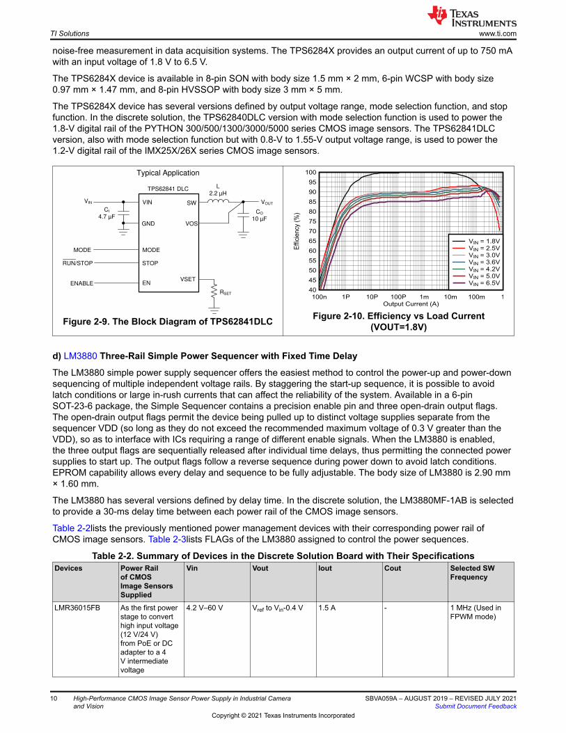
The TPS6284X device has several versions defined by output voltage range, mode selection function, and stop function. In the discrete solution, the TPS62840DLC version with mode selection function is used to power the 1.8-V digital rail of the PYTHON 300/500/1300/3000/5000 series CMOS image sensors. The TPS62841DLC version, also with mode selection function but with 0.8-V to 1.55-V output voltage range, is used to power the 1.2-V digital rail of the IMX25X/26X series CMOS image sensors.
CI 4.7 µF
CO
10 µF
VOUT
MODE
RUN/STOP
ENABLEVSET
EN
STOP
MODE
GND
VINVIN
RSET
Typical Application
TPS62841 DLC
SW
VOS
L2.2 µH
Figure 2-9. The Block Diagram of TPS62841DLC
Output Current (A)
Effi
ciency
(%
)40
45
50
55
60
65
70
75
80
85
90
95
100
100n 1P 10P 100P 1m 10m 100m 1
VIN = 1.8VVIN = 2.5VVIN = 3.0VVIN = 3.6VVIN = 4.2VVIN = 5.0VVIN = 6.5V
Figure 2-10. Efficiency vs Load Current (VOUT=1.8V)
d) LM3880 Three-Rail Simple Power Sequencer with Fixed Time Delay
The LM3880 simple power supply sequencer offers the easiest method to control the power-up and power-down sequencing of multiple independent voltage rails. By staggering the start-up sequence, it is possible to avoid latch conditions or large in-rush currents that can affect the reliability of the system. Available in a 6-pin SOT-23-6 package, the Simple Sequencer contains a precision enable pin and three open-drain output flags. The open-drain output flags permit the device being pulled up to distinct voltage supplies separate from the sequencer VDD (so long as they do not exceed the recommended maximum voltage of 0.3 V greater than the VDD), so as to interface with ICs requiring a range of different enable signals. When the LM3880 is enabled, the three output flags are sequentially released after individual time delays, thus permitting the connected power supplies to start up. The output flags follow a reverse sequence during power down to avoid latch conditions. EPROM capability allows every delay and sequence to be fully adjustable. The body size of LM3880 is 2.90 mm × 1.60 mm.
The LM3880 has several versions defined by delay time. In the discrete solution, the LM3880MF-1AB is selected to provide a 30-ms delay time between each power rail of the CMOS image sensors.
Table 2-2lists the previously mentioned power management devices with their corresponding power rail of CMOS image sensors. Table 2-3lists FLAGs of the LM3880 assigned to control the power sequences.
Table 2-2. Summary of Devices in the Discrete Solution Board with Their SpecificationsDevices Power Rail
of CMOS Image Sensors Supplied
Vin Vout Iout Cout Selected SW Frequency
LMR36015FB As the first power stage to convert high input voltage (12 V/24 V) from PoE or DC adapter to a 4 V intermediate voltage
4.2 V–60 V Vref to Vin-0.4 V 1.5 A - 1 MHz (Used in FPWM mode)
TI Solutions www.ti.com
10 High-Performance CMOS Image Sensor Power Supply in Industrial Camera and Vision
SBVA059A – AUGUST 2019 – REVISED JULY 2021Submit Document Feedback
Copyright © 2021 Texas Instruments Incorporated
Table 2-2. Summary of Devices in the Discrete Solution Board with Their Specifications (continued)Devices Power Rail
of CMOS Image Sensors Supplied
Vin Vout Iout Cout Selected SW Frequency
TPS7A87 VDD_33 and AVDD (LDO1 of TPS7A87)VDD_PIXEL and OVDD (LDO2 of TPS7A87)
1.4 V–6.5 V 0.8 V to 5.2 V (Vdo=0.1 V at 0.5 A)
500 mA ≥10 uF -
TPS7A90 VDD_18 and DVDD
1.4 V–6.5 V 0.8 V to 5.7 V (Vdo=0.1 V at 0.5 A)
500 mA ≥10 uF -
TPS62840DLC VDD_18 1.8 V–6.5 V 1.8 V–3.3 V 750 mA 3 uF to 40 uF 1.8 MHz (Used in FPWM mode)
TPS62841DLC DVDD 1.8 V–6.5 V 0.8 V–1.55 V 750 mA 3 uF to 40 uF 1.8 MHz (Used in FPWM mode)
Table 2-3. Setup of the LM3880 with Specific Power Sequencing RequirementsCMOS Image Sensor Controlled Power Rail FLAG in LM3880 Power Up Order Power Down OrderPYTHON 300/500/1300/3000/5000
VDD_33 FLAG2 2 2
VDD_PIXEL FLAG3 3 1
VDD_18 FLAG1 1 3
IMX25X/26X AVDD FLAG3 3 1
OVDD FLAG2 2 2
DVDD FLAG1 1 3
2.2.2 Consideration
a) Setting Output Voltages
The output voltages of the LMR36015, TPS7A87, and TPS7A90 can be set up by defining resistor divider networks. Equation 1 can be used to calculate output voltages for the TPS7A87 and TPS7A90. This resistive network must provide a current greater than or equal to 5 μA for optimum noise performance. Vref is nominally 0.8 V. R1 = R2 Vout/Vref − 1Vref max /R2 > 5 µ A (1)
• R1 is the resistor between FB pin and OUT pin of TPS7A87 or TPS7A90.• R2 is the resistor between FB pin and ground.
In the LM36015, the voltage divider network is comprised of RFBT and RFBB. The output voltage can be calculated using Equation 2. The recommended value for RFBT is 100 kΩ, with a maximum value of 1 MΩ. If 1 MΩ is selected for RFBT, then a feed-forward capacitor must be used across this resistor to provide an adequate loop phase margin. Vref is nominally 1 V.RFBT = RFBB Vout/Vref− 1 (2)
The output voltage of the TPS62840 or TPS62841 is set by a single external resistor connected between the VSET and GND pins. For more details, please refer to the TPS6284X data sheet.
Table 2-4. Setup for Required Output Voltages of the LMR36015, TPS7A87, TPS7A90, and TPS62840Device Output Voltage Required Value of R1 Value of R2LMR36015FB 4 V 100 KΩ 33.2 KΩ
TPS7A87 3.3 V 33.2 KΩ 10.7 KΩ
1.8 V 13.7 KΩ 11 KΩ
www.ti.com TI Solutions
SBVA059A – AUGUST 2019 – REVISED JULY 2021Submit Document Feedback
High-Performance CMOS Image Sensor Power Supply in Industrial Camera and Vision
11
Copyright © 2021 Texas Instruments Incorporated
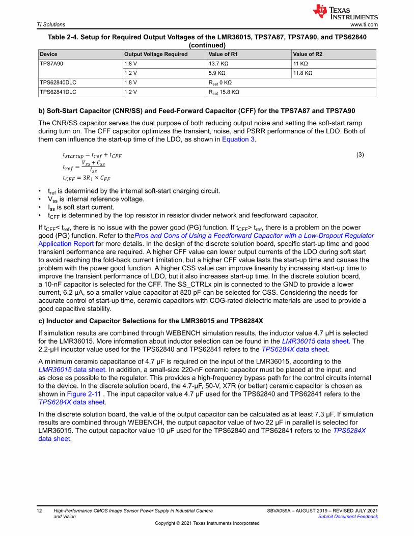
Table 2-4. Setup for Required Output Voltages of the LMR36015, TPS7A87, TPS7A90, and TPS62840 (continued)
Device Output Voltage Required Value of R1 Value of R2TPS7A90 1.8 V 13.7 KΩ 11 KΩ
1.2 V 5.9 KΩ 11.8 KΩ
TPS62840DLC 1.8 V Rset 0 KΩ
TPS62841DLC 1.2 V Rset 15.8 KΩ
b) Soft-Start Capacitor (CNR/SS) and Feed-Forward Capacitor (CFF) for the TPS7A87 and TPS7A90
The CNR/SS capacitor serves the dual purpose of both reducing output noise and setting the soft-start ramp during turn on. The CFF capacitor optimizes the transient, noise, and PSRR performance of the LDO. Both of them can influence the start-up time of the LDO, as shown in Equation 3.tstartup = tref+ tCFFtref = Vss+ CssIsstCFF = 3R1 × CFF
(3)
• tref is determined by the internal soft-start charging circuit.• Vss is internal reference voltage.• Iss is soft start current.• tCFF is determined by the top resistor in resistor divider network and feedforward capacitor.
If tCFF< tref, there is no issue with the power good (PG) function. If tCFF> tref, there is a problem on the power good (PG) function. Refer to thePros and Cons of Using a Feedforward Capacitor with a Low-Dropout Regulator Application Report for more details. In the design of the discrete solution board, specific start-up time and good transient performance are required. A higher CFF value can lower output currents of the LDO during soft start to avoid reaching the fold-back current limitation, but a higher CFF value lasts the start-up time and causes the problem with the power good function. A higher CSS value can improve linearity by increasing start-up time to improve the transient performance of LDO, but it also increases start-up time. In the discrete solution board, a 10-nF capacitor is selected for the CFF. The SS_CTRLx pin is connected to the GND to provide a lower current, 6.2 μA, so a smaller value capacitor at 820 pF can be selected for CSS. Considering the needs for accurate control of start-up time, ceramic capacitors with COG-rated dielectric materials are used to provide a good capacitive stability.
c) Inductor and Capacitor Selections for the LMR36015 and TPS6284X
If simulation results are combined through WEBENCH simulation results, the inductor value 4.7 µH is selected for the LMR36015. More information about inductor selection can be found in the LMR36015 data sheet. The 2.2-µH inductor value used for the TPS62840 and TPS62841 refers to the TPS6284X data sheet.
A minimum ceramic capacitance of 4.7 μF is required on the input of the LMR36015, according to the LMR36015 data sheet. In addition, a small-size 220-nF ceramic capacitor must be placed at the input, and as close as possible to the regulator. This provides a high-frequency bypass path for the control circuits internal to the device. In the discrete solution board, the 4.7-μF, 50-V, X7R (or better) ceramic capacitor is chosen as shown in Figure 2-11 . The input capacitor value 4.7 µF used for the TPS62840 and TPS62841 refers to the TPS6284X data sheet.
In the discrete solution board, the value of the output capacitor can be calculated as at least 7.3 μF. If simulation results are combined through WEBENCH, the output capacitor value of two 22 µF in parallel is selected for LMR36015. The output capacitor value 10 µF used for the TPS62840 and TPS62841 refers to the TPS6284X data sheet.
TI Solutions www.ti.com
12 High-Performance CMOS Image Sensor Power Supply in Industrial Camera and Vision
SBVA059A – AUGUST 2019 – REVISED JULY 2021Submit Document Feedback
Copyright © 2021 Texas Instruments Incorporated

IN11
IN12
GND3
IN24
IN25
EN26
NR/SS27
SS_CTRL28
PG29
FB210
OUT211
OUT212
GND13
OUT114
OUT115
FB116
PG117
SS_CTRL118
NR/SS119
EN120
PAD21
TPS7A8701RTJR
U1
OUT1
OUT2
FB3
GND4
PG5
SS_CTRL6
EN7
NR/SS8
IN9
IN10
PAD11
TPS7A9001DSKR
U2
VCC1
GND2
EN3
FLAG34
FLAG25
FLAG16
LM3880MF-1AB/NOPB
U3
VCC_4V
10V
10uF
CIN1
GND
VCC_4V
10V
10uF
CIN2
GND
GND
GND
GND
GND
25V
0.01µF
Cff1
25V
820pF
CNR/SS2
25V
820pF
CNR/CSS1
GND
GND
25V
0.01µF
Cff2
GND
GND
10V
10uF
CIN3
GND
25V
820pF
CNR/CSS3
GND
GND GND
GND
25V
0.01µF
Cff3
GND
13.7kR31
11.0k
R32
100k
R1
100k
R2
100k
R3
GND
FLAG1
FLAG2
FLAG3
PGND1
VIN2
NC3
BOOT4
VCC5
AGND6
FB7
PG8
EN9
VIN10
PGND11
SW12
LMR36015FBRNXR
U4
50V
4.7uF
CIN
1µF
10V
Ccc
GND
100k
Rfbt
33.2k
Rfbb
VCC_4V
100k
RPG
1
2G
TP2
1
2G
TP3
1
2G
TP4
GND
100k
RPG1
100k
RPG2
100k
RPG3
GND
50V
22pF
CFF
10V
10uF
COUT1
10V
10uF
COUT2
10V
10uF
COUT3
33.2k
R11
33.2k
R21
10.7k
R12
10.7k
R22
GND
GND
GND
1
2
J1
1
2
J2
1
2
J3
4.7uH
L1
25V
0.1uF
Cboot
1 2
3 4
J0 12
34
J4
1
2G
TP1
VCC_4V
VCC_4V
EN4
VOS8
GND1
MODE3
VSET5
SW7
VIN2
STOP6
TPS62840DLCR
U2_DC
10V
4.7uF
CIN4
GND
GND
2.2uH
L2
GND
GND
10µF
10V
COUT4
GND
1
2G
TP11
1 2
J9
12
34
J10
220nF
50V
CINx1
220nF
50V
CINx2
22µF
10V
Cout
22µF
10V
Coutx
TP13
5004
TP14
TP15
TP16
22.0k
Re1
10.0k
Re2
1 2
J5
1 2
J6
1
2
3
J8
1
2
3
JEN
TP9 TP10 TP12TP8
Analog
Pixel/Interface
Digital
FLAG1
FLAG2
FLAG3
Analog
Pixel/Interface
Digital
Digital
Digital
Pixel/Interface
Pixel/Interface
Analog
Analog
Digital
1 2
3 4
5 6
J_FLAG1
1 2
3 4
5 6
J_FLAG2
1 2
3 4
5 6
J_FLAG3
0
0OHM
Figure 2-11. The Schematic of Discrete Solution
2.2.3 Discrete Solution PCB Board Description
The discrete solution PCB board is shown in Figure 2-12. The body size is 25 mm × 24 mm without considering test points. J6 is used to disconnect the first and second power stage and then test them individually. J8 is used to choose either the TPS7A90 or TPS6284X for powering the digital rail of the CMOS image sensors. J_FLAG1, J_FLAG2, and J_FLAG3 are used to select powering sequences where row 1 is selected for analog rail, row 2 is selected for the PIXEL or interface rail, and row 3 is selected for digital rail.
www.ti.com TI Solutions
SBVA059A – AUGUST 2019 – REVISED JULY 2021Submit Document Feedback
High-Performance CMOS Image Sensor Power Supply in Industrial Camera and Vision
13
Copyright © 2021 Texas Instruments Incorporated
Figure 2-12. PCB Board of Discrete Solution
2.3 Design of the TPS65000 Solution2.3.1 Device Selection
TPS65000 2.25 MHz Step-Down Converter with Dual LDOs and SVS Power Management IC (PMIC)
The TPS6500XX devices are single-chip power management (PWM) ICs for portable applications. It contains a single step-down converter and two low-dropout (LDO) regulators. The step-down converter enters a low-power mode at light load for maximum efficiency across the widest possible range of load currents. For low-noise applications, the devices can be forced into fixed-frequency PWM through a pin. The step-down converter is small because of the small inductor and capacitors. The step-down converter has a power good status output for sequencing. The LDOs can supply 300 mA and operate with an input voltage range from 1.6 V to 6 V. A step-down converter or main battery can power the LDOs directly. The step-down converter and the LDOs have separate voltage inputs that enable maximum design and sequencing flexibility. The TPS6500XX device is available in the VQFN (16) package with body size 3 mm × 3 mm, and WQFN (20) with body size 3 mm × 3 mm.
The TPS6500XX device has several versions defined by output voltages and whether there is supply voltage supervisor or not. In this solution, the TPS65000 version is used.
TI Solutions www.ti.com
14 High-Performance CMOS Image Sensor Power Supply in Industrial Camera and Vision
SBVA059A – AUGUST 2019 – REVISED JULY 2021Submit Document Feedback
Copyright © 2021 Texas Instruments Incorporated

VINDCDC
EN_DCDC
MODE
MR
RSTSNS
VINLDO1
EN_LDO1
VINLDO2
EN_LDO2
Supply
Voltage
Supervisor
Buck Converter
600 mA
Oscillator
SSCG
LDO1
300 mA
LDO2
300 mA
TPS65000/TPS65001
Bandgap Reference
SW
FB_DCDC
PG
TRST
RST
VLDO1
FB_LDO1
VLDO2
FB_LDO2
PGND
AGND
3 x 3 mm2QFN
Joint Function/Pin TPS65001 Only Function/Pin
Figure 2-13. Block Diagram of the TPS65000
As shown in Table 2-5, and compared with the specifications in Table 1-1, it can be seen that the TPS65000 solution can support powering the PYTHON 300/500/1300 and IMX25X/26X CMOS image sensors.
Table 2-5. Summary of Components in TPS65000 with Their SpecificationsComponent Power Rail
of CMOS Image Sensors Supplied
Vin Vout Iout Cout Selected SW Frequency
LDO1 VDD_PIXEL and OVDD
1.6 V–6 V 0.7 V to VINLDO-Vdo (Vdo=0.37 V)
300 mA ≥10 uF -
LDO2 VDD_33 and AVDD
1.6 V–6 V 0.7 V to VINLDO-Vdo (Vdo=0.37 V)
300 mA ≥10 uF -
Buck VDD_18 and DVDD
2.3 V–6 V 0.6 V-VinDC/DC 600 mA 10 uF–22 uF 2.25 MHz (Used in FPWM mode)
2.3.2 Configurations of theTPS65000 Solution
As introduced in Section 2.1, the TPS65000 solution consists of the LMR36015 from the discrete solution board, TPS65000EVM board, and LM3880EVM board to provide power supplies for PYTHON 300/500/1300 and IMX25X/26X CMOS image sensors. The output voltage of the LMR36015 is set to 4 V. Several resistors need to be changed according to Table 2-6 to provide certain output voltage for each rail of the CMOS image sensors. The LM3880EVM can be configured as shown in Table 2-7 in order to provide the specific powering sequences of each rail of the CMOS image sensors.
Table 2-6. Set Up for Required Output Voltages of the TPS65000EVM BoardCMOS Image Sensor Power Rail Of CMOS
Image SensorsTPS65000 Voltage Top-resistor In
Corresponding Resistor Divider Network
Bottom-resistor In Corresponding Resistor Divider Network
PYTHON 300/500/1300
V_33 LDO2 3.3 V 162 KΩ 28.7 KΩ
V_PIXEL LDO1 3.3 V 162 KΩ 28.7 KΩ
V_18 Buck 1.8 V 953 KΩ 470 KΩ
www.ti.com TI Solutions
SBVA059A – AUGUST 2019 – REVISED JULY 2021Submit Document Feedback
High-Performance CMOS Image Sensor Power Supply in Industrial Camera and Vision
15
Copyright © 2021 Texas Instruments Incorporated

Table 2-6. Set Up for Required Output Voltages of the TPS65000EVM Board (continued)CMOS Image Sensor Power Rail Of CMOS
Image SensorsTPS65000 Voltage Top-resistor In
Corresponding Resistor Divider Network
Bottom-resistor In Corresponding Resistor Divider Network
IMX25X/26X AVDD LDO2 3.3 V 162 KΩ 28.7 KΩ
OVDD LDO1 1.8 V 470 KΩ 180 KΩ
DVDD Buck 1.2 V 475 KΩ 475 KΩ
Table 2-7. Connecting the LM3880EVM Board with the TPS65000EVM BoardCMOS Image Sensor Controlled Power Rail FLAG from the LM3880EVM
BoardPin Connected in the TPS65000EVM Board
PYTHON 300/500/1300 V_33 FLAG2 Pin 2 of JP2 (ENLDO2)
V_PIXEL FLAG3 Pin 2 of JP1 (ENLDO1)
V_18 FLAG1 Pin 2 of JP6 (ENDCDC)
IMX25X/26X AVDD FLAG3 Pin 2 of JP2 (ENLDO2)
OVDD FLAG2 Pin 2 of JP1 (ENLDO1)
DVDD FLAG1 Pin 2 of JP6 (ENDCDC)
2.4 Design of TPS650330-Q1 Solution2.4.1 Device Selection
TPS650330-Q1 Three Step-Down Converters with One High PSRR LDO Integrated Power Management IC (PMIC)
The TPS650330-Q1 device is a highly integrated power management IC for automotive camera modules. This device combines three step-down converters and one low-dropout (LDO) regulator. The BUCK1 step-down converter has an input voltage range up to 18.3 V for connections to Power over Coax (PoC). All converters operate in a forced fixed-frequency PWM mode. The LDO can supply 300 mA and operate with an input voltage range from 3.0 V to 5.5 V. The step-down converters and the LDO have separate voltage inputs that enable maximum design and sequencing flexibility. The TPS650330-Q1 is available in a 24-pin VQFN package (4.0 mm × 4.0 mm).
TI Solutions www.ti.com
16 High-Performance CMOS Image Sensor Power Supply in Industrial Camera and Vision
SBVA059A – AUGUST 2019 – REVISED JULY 2021Submit Document Feedback
Copyright © 2021 Texas Instruments Incorporated

BUCK13.0 V to 4.0 V
1.5 A
Safety PowerDomain Circuits
10 F
PVIN_B14 V < VI < 18.3 V
VSYS_S
VSYS
Gate DriveLDO
AGND
AGND
GND
REFSYS
1 F
PWR_PAD
PWR_PAD
BUCK30.9 V to 1.9 V
1200 mA
LDO2.7 V to 3.3 V
300 mAAGND
I2C and Digital Logic
0.1 F
10 F
1 F
10 FBUCK20.9 V to 1.9 V
1200 mA
10 F
1 F1 F
PWR_PAD
BOOTCAP
LX_B1
FB_B1
1.5 µH
VREG
LX_B2 1 µH
FB_B2
LX_B3 1 µH
FB_B3
nINT
nRSTOUT
GPIO
VIO
DGND
SEQ
SCL
SDA
1 F
10 F
10 F
VINLDO
PVIN_B3
PVIN_B2
AGND
V1P8_INT
10 F
1.8 V
1.2 V / 1.1 V
3.3 V / 2.8 V / 2.9 V
Figure 2-14. Block Diagram of the TPS650330-Q1
As shown in Table 2-8 and compared with the specifications in Table 1-1, it can be seen that the TPS650330-Q1 solution can support powering IMX25X/26X CMOS image sensors.
www.ti.com TI Solutions
SBVA059A – AUGUST 2019 – REVISED JULY 2021Submit Document Feedback
High-Performance CMOS Image Sensor Power Supply in Industrial Camera and Vision
17
Copyright © 2021 Texas Instruments Incorporated

Table 2-8. Summary of Components in the TPS650330-Q1 with Their SpecificationsComponent Power Rail
of CMOS Image Sensors Supplied
Vin Vout Iout Cout Selected SW Frequency
LDO AVDD 3 V–5.5 V 2.7 V–3.3 V(Vdo=150mV–300mV)
300 mA 1 uF–4 uF -
Buck1 As the first power stage to transform high input voltage (12 V) from PoE or DC adapter to a 4-V intermediate voltage
4 V–18.3 V 3 V-4 V 1500 mA 6.8 uF–14 uF 2.3 MHz FPWM
Buck2 DVDD 3 V–5.5 V 0.9 V-1.9 V 1200 mA 6.8 uF–12 uF 2.3 MHz FPWM
Buck3 OVDD 3 V–5.5 V 0.9 V-1.9 V 1200 mA 6.8 uF–12 uF 2.3 MHz FPWM
2.4.2 Configurations of the TPS650330-Q1 Solution
Hardware configuration can be done according to the TPS650330-Q1EVM User’s Guide, which is available on request at the TPS650330-Q1 product page. As shown in Figure 2-1, buck 1 in the TPS650330-Q1 is used as the first power stage to convert the 12-V input voltage to 4-V intermediate voltage. Buck 2 in the TPS650330-Q1 is used to power 1.2 V for the digital rail, and buck 3 powers 1.8 V for the interface rail. The LDO in the TPS650330-Q1 sets the analog rail to 3.3 V. These configurations can be set up in the TPS650330-Q1 GUI. For powering IMX25X/26X CMOS image sensors, the power-on sequences are set to 20-ms delay time between every power rail and the power-off sequences are set to 4-ms delay time between every power rail.
TI Solutions www.ti.com
18 High-Performance CMOS Image Sensor Power Supply in Industrial Camera and Vision
SBVA059A – AUGUST 2019 – REVISED JULY 2021Submit Document Feedback
Copyright © 2021 Texas Instruments Incorporated
3 Test ResultsAll three solutions have been tested for power sequencing performance, efficiency, line transient and load transient. Besides, the 4-V intermediate voltage is adjusted to identify the relationship between the intermediate voltage of a multi-stage system and the whole system efficiency.
3.1 Test Results of the Discrete Solution Board3.1.1 Setup
As introduced in previous sections, the discrete solution supports power supplies of all the CMOS image sensors listed in Table 1-1, which may require large capacitors and high current consumption up to 500 mA. Furthermore, the discrete solution board can be configured for six cases, as shown in Table 3-1.
Table 3-1. Configurations of the Discrete Solution Board for Six CasesCMOS Image Sensors Case Case Number Configurations of Discrete
Solution BoardPYTHON 300/500/1300 LMR36015+TPS7A87+TPS7A90
+LM3880 (30-ms delay)1 1. Follow Table 1-1 and Table
2-4 to set up the right voltage for each power rail.
2. Put headers in J5, J6, between pin 1 and pin 2 in J8 for TPS7A90 or between pin 2 and pin 3 in J8 for TPS62840, row 2 in J_FLAG1, row 3 in J_FLAG2 and row 1 in J_FLAG3.
LMR36015+TPS7A87+TPS62840+LM3880 (30-ms delay)
2
PYTHON 3000/5000 LMR36015+TPS7A87+TPS7A90+LM3880 (30-ms delay)
3
LMR36015+TPS7A87+TPS62840+LM3880 (30-ms delay)
4
IMX25X/26X LMR36015+TPS7A87+TPS7A90+LM3880 (30-ms delay)
5 1. Follow Table 1-1 and Table 2-4 to set up the right voltage for each power rail.
2. Put headers in J5, J6, between pin 1 and pin 2 in J8 for TPS7A90 or between pin 2 and pin 3 in J8 for TPS62841, row 3 in J_FLAG1, row 2 in J_FLAG2 and row 1 in J_FLAG3.
LMR36015+TPS7A87+TPS62841+LM3880 (30-ms delay)
6
a) Power Sequencing Test Setup
For each case shown in Table 3-1, the power sequence of each rail is tested under 12-V input voltage for the whole system. The LM3880 is enabled by an external signal. In this test, the external signal is provided by a waveform generator. Three tip-barrel test probes are separately put in the output of each power rail in front of loads. A current probe is used to observe the current performance of each power rail.
b) Efficiency Test Setup
In total, four sets of digital multi-meters are used. In each set, one digital multi-meter is set as current meter (AM), and another is set as voltage meter (VM). One set is placed between the DC power supply and the input of the discrete solution board to measure input power. The other three sets are separately placed in front of three outputs.
3.1.2 Test Results
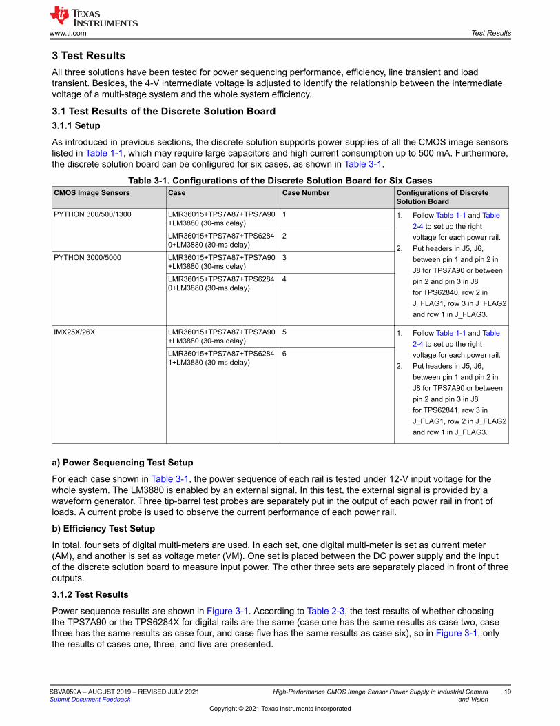
Power sequence results are shown in Figure 3-1. According to Table 2-3, the test results of whether choosing the TPS7A90 or the TPS6284X for digital rails are the same (case one has the same results as case two, case three has the same results as case four, and case five has the same results as case six), so in Figure 3-1, only the results of cases one, three, and five are presented.
www.ti.com Test Results
SBVA059A – AUGUST 2019 – REVISED JULY 2021Submit Document Feedback
High-Performance CMOS Image Sensor Power Supply in Industrial Camera and Vision
19
Copyright © 2021 Texas Instruments Incorporated
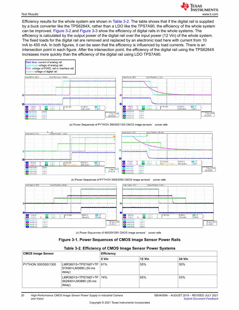
Efficiency results for the whole system are shown in Table 3-2. The table shows that if the digital rail is supplied by a buck converter like the TPS6284X, rather than a LDO like the TPS7A90, the efficiency of the whole system can be improved. Figure 3-2 and Figure 3-3 show the efficiency of digital rails in the whole systems. The efficiency is calculated by the output power of the digital rail over the input power (12 Vin) of the whole system. The fixed loads for the digital rail are removed and replaced by an electronic load here with current from 10 mA to 450 mA. In both figures, it can be seen that the efficiency is influenced by load currents. There is an intersection point in each figure. After the intersection point, the efficiency of the digital rail using the TPS6284X increases more quickly than the efficiency of the digital rail using LDO TPS7A90.
Figure 3-1. Power Sequences of CMOS Image Sensor Power Rails
Table 3-2. Efficiency of CMOS Image Sensor Power SystemsCMOS Image Sensor Efficiency
5 Vin 12 Vin 24 VinPYTHON 300/500/1300 LMR36015+TPS7A87+TP
S7A90+LM3880 (30-ms delay)
61% 55% 50%
LMR36015+TPS7A87+TPS62840+LM3880 (30-ms delay)
74% 65% 53%
Test Results www.ti.com
20 High-Performance CMOS Image Sensor Power Supply in Industrial Camera and Vision
SBVA059A – AUGUST 2019 – REVISED JULY 2021Submit Document Feedback
Copyright © 2021 Texas Instruments Incorporated
Table 3-2. Efficiency of CMOS Image Sensor Power Systems (continued)PYTHON 3000/5000 LMR36015+TPS7A87+TP
S7A90+LM3880 (30-ms delay)
61% 58% 53%
LMR36015+TPS7A87+TPS62840+LM3880 (30-ms delay)
72% 68% 61%
IMX25X/26X LMR36015+TPS7A87+TPS7A90+LM3880 (30-ms delay)
55% 43% 36%
LMR36015+TPS7A87+TPS62841+LM3880 (30-ms delay)
71% 62% 50%
Output Current (A)
Effic
ien
cy (
%)
0 0.05 0.1 0.15 0.2 0.25 0.3 0.35 0.4 0.455
10
15
20
25
30
35
40
45
50
55
60
65
70
75
D001
Efficiency_TPS7A90Efficiency_TPS62840
Figure 3-2. Efficiency of the Digital Rail Supplied by TPS7A90 or TPS62840 in PYTHON 300/500/1300
CMOS Image Sensors
Output Current (A)
Effic
ien
cy (
%)
0 0.05 0.1 0.15 0.2 0.25 0.3 0.35 0.4 0.450
10
20
30
40
50
60
70
D002
Efficiency_TPS7A90Efficiency_TPS62841
Figure 3-3. Efficiency of the Digital Rail Supplied by TPS7A90 or TPS62841 in IMX25X/26X CMOS
Image Sensors
3.2 Test Results of TPS65000 SolutionsConfigurations of the TPS65000 solutions are described in Section 2.3.2 and the repeating testing procedure in Section 3. The test results of TPS65000 solutions are shown as follows. Figure 3-4presents the power sequences of the power rails of the CMOS image sensors. Table 3-3 summarizes the efficiency of the whole system for powering the PYTHON 300/500/1300 and IMX25X/26X CMOS image sensors. The efficiency of the whole system can be improved even more than the discrete solution according to Section 4.3.
www.ti.com Test Results
SBVA059A – AUGUST 2019 – REVISED JULY 2021Submit Document Feedback
High-Performance CMOS Image Sensor Power Supply in Industrial Camera and Vision
21
Copyright © 2021 Texas Instruments Incorporated

Figure 3-4. Power Sequences of the Power Rails of the CMOS Image Sensors Using the TPS65000 Solutions
Table 3-3. Efficiency of the Whole System Using the TPS65000 SolutionsCMOS Images Sensor Efficiency
5 Vin 12 Vin 24 VinPYTHON 300/500/1300 75% 66% 54%
IMX25X/26X 72% 63% 51%
3.3 Test Results of the TPS650330-Q1 SolutionsThe following configurations of TPS650330-Q1 solutions are described in Section 2.4.2 and repeating test procedures in Section 3. Test results of the TPS650330-Q1 solutions are shown as follows. Section 1 presents power sequences for the power rails of IMX25X/26X CMOS image sensors. Table 3-4 summarizes the efficiency of the whole system for powering IMX25X/26X CMOS image sensors. The efficiency of the whole system can be further improved.
Test Results www.ti.com
22 High-Performance CMOS Image Sensor Power Supply in Industrial Camera and Vision
SBVA059A – AUGUST 2019 – REVISED JULY 2021Submit Document Feedback
Copyright © 2021 Texas Instruments Incorporated
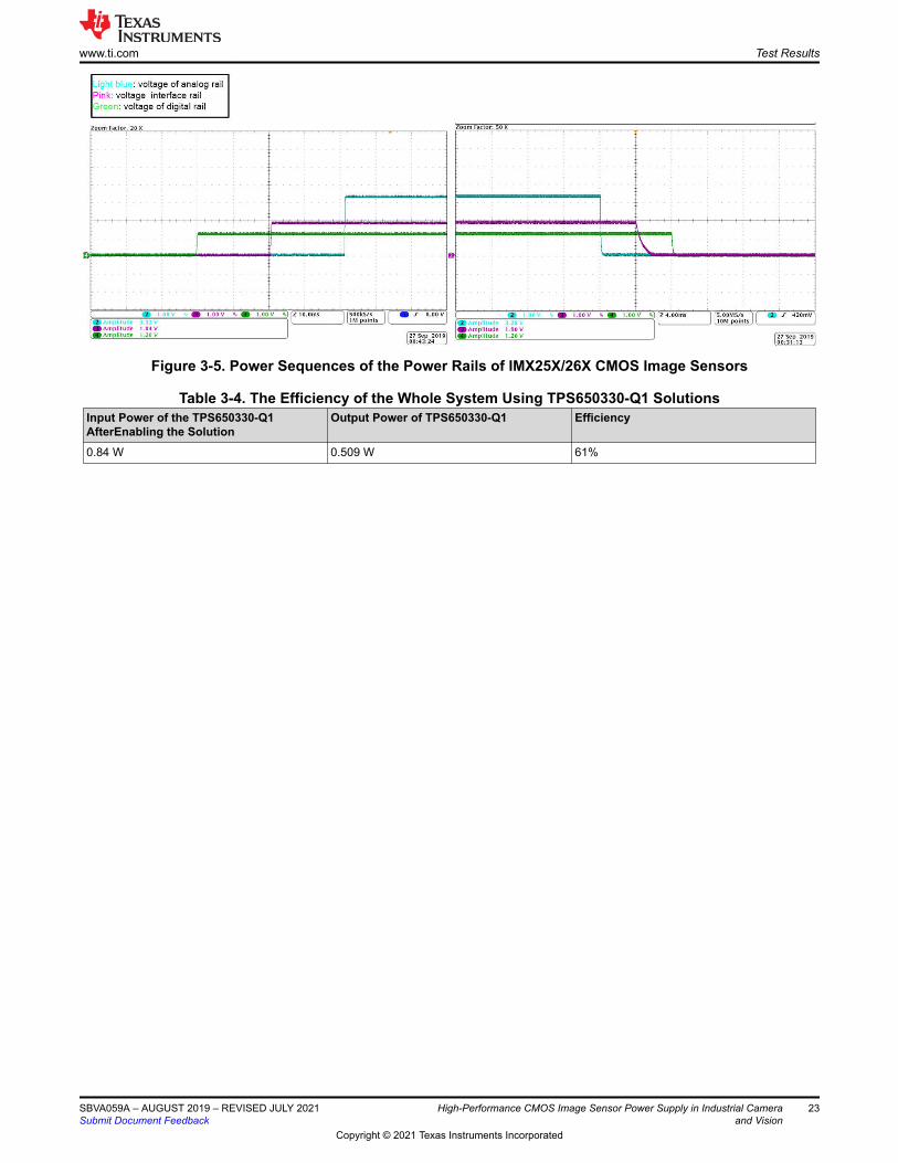
Figure 3-5. Power Sequences of the Power Rails of IMX25X/26X CMOS Image Sensors
Table 3-4. The Efficiency of the Whole System Using TPS650330-Q1 SolutionsInput Power of the TPS650330-Q1 AfterEnabling the Solution
Output Power of TPS650330-Q1 Efficiency
0.84 W 0.509 W 61%
www.ti.com Test Results
SBVA059A – AUGUST 2019 – REVISED JULY 2021Submit Document Feedback
High-Performance CMOS Image Sensor Power Supply in Industrial Camera and Vision
23
Copyright © 2021 Texas Instruments Incorporated

4 Analysis4.1 Power Sequence Modification of PYTHON Series CMOS Image SensorsThere is no limitation on the maximum power-up and power-off time in the datasheet of PYTHON series CMOS Image Sensor. In order to keep the power-off sequence in a safety range, the LM3880 with longer delay time can be used. Figure 4-1 shows the power sequences of the power rails of PYTHON 300/500/1300 CMOS image sensors using LM3880 with 120-ms delay.
Figure 4-1. Power Sequence of the Power Rails of PYTHON 300/500/1300 CMOS Image Sensors Using the 120-ms Delay Time LM3880
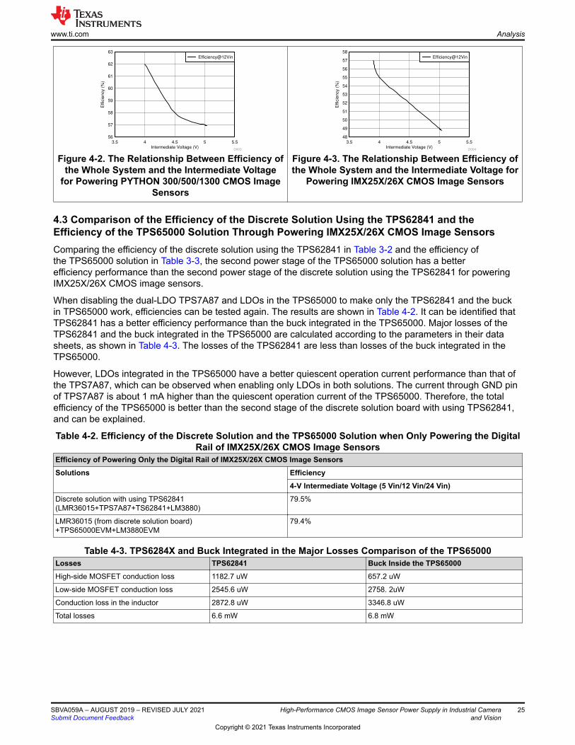
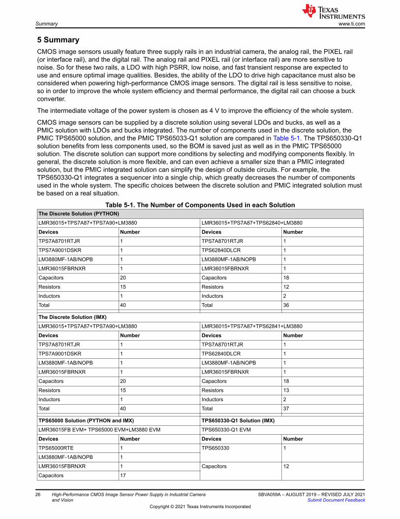
4.2 Efficiency of the Whole System Influenced by Changing the Intermediate VoltageBased on the TPS65000 solution, the 4-V intermediate voltage supplied by the LMR36015 in the discrete board is adjusted in this section. A more suitable intermediate voltage when designing power rails can be considered according to the relationship between the efficiency of the whole system and the intermediate voltage.
Considering the output voltage range of the buck, dropout voltages of the LDO, and accuracy of output voltages in the TPS65000, the 4-V intermediate voltage powering PYTHON 300/500/1300 case is changed into 4.5 V and 5 V to repeat efficiency tests for the whole power system. The 4-V intermediate voltage powering the IMX25X/26X case is adjusted into 3.9 V, 4.5 V, and 5 V. Table 4-1 lists resistors values for adjusting the output voltages of the LMR36015 into 3.9 V, 4.5 V, and 5 V. As shown in Figure 4-2 and Figure 4-3 , the efficiency decreases when the intermediate voltage increases. The increasing intermediate voltage can improve the efficiency of the first power stage (the LMR36015), but it causes more power dissipation on LDOs. For this system, power dissipation on LDOs have more impact on the whole system efficiency.
Table 4-1. Selections of Resistors for the LMR36015 to Output 3.9V, 4V, 5V and 4.5VOutput Voltage of the LMR36015 RFBT RFBB
3.9 V 100 K 34.8 KΩ
5 V 100 K 24.9 KΩ
4.5 V 100 K 28.7 KΩ
Analysis www.ti.com
24 High-Performance CMOS Image Sensor Power Supply in Industrial Camera and Vision
SBVA059A – AUGUST 2019 – REVISED JULY 2021Submit Document Feedback
Copyright © 2021 Texas Instruments Incorporated
Intermediate Voltage (V)
Effic
ien
cy (
%)
3.5 4 4.5 5 5.556
57
58
59
60
61
62
63
D003
Efficiency@12Vin
Figure 4-2. The Relationship Between Efficiency of the Whole System and the Intermediate Voltage
for Powering PYTHON 300/500/1300 CMOS Image Sensors
Intermediate Votage (V)
Effic
ien
cy (
%)
3.5 4 4.5 5 5.548
49
50
51
52
53
54
55
56
57
58
D004
Efficiency@12Vin
Figure 4-3. The Relationship Between Efficiency of the Whole System and the Intermediate Voltage for
Powering IMX25X/26X CMOS Image Sensors
4.3 Comparison of the Efficiency of the Discrete Solution Using the TPS62841 and the Efficiency of the TPS65000 Solution Through Powering IMX25X/26X CMOS Image SensorsComparing the efficiency of the discrete solution using the TPS62841 in Table 3-2 and the efficiency of the TPS65000 solution in Table 3-3, the second power stage of the TPS65000 solution has a better efficiency performance than the second power stage of the discrete solution using the TPS62841 for powering IMX25X/26X CMOS image sensors.
When disabling the dual-LDO TPS7A87 and LDOs in the TPS65000 to make only the TPS62841 and the buck in TPS65000 work, efficiencies can be tested again. The results are shown in Table 4-2. It can be identified that TPS62841 has a better efficiency performance than the buck integrated in the TPS65000. Major losses of the TPS62841 and the buck integrated in the TPS65000 are calculated according to the parameters in their data sheets, as shown in Table 4-3. The losses of the TPS62841 are less than losses of the buck integrated in the TPS65000.
However, LDOs integrated in the TPS65000 have a better quiescent operation current performance than that of the TPS7A87, which can be observed when enabling only LDOs in both solutions. The current through GND pin of TPS7A87 is about 1 mA higher than the quiescent operation current of the TPS65000. Therefore, the total efficiency of the TPS65000 is better than the second stage of the discrete solution board with using TPS62841, and can be explained.
Table 4-2. Efficiency of the Discrete Solution and the TPS65000 Solution when Only Powering the Digital Rail of IMX25X/26X CMOS Image Sensors
Efficiency of Powering Only the Digital Rail of IMX25X/26X CMOS Image SensorsSolutions Efficiency
4-V Intermediate Voltage (5 Vin/12 Vin/24 Vin)Discrete solution with using TPS62841 (LMR36015+TPS7A87+TS62841+LM3880)
79.5%
LMR36015 (from discrete solution board)+TPS65000EVM+LM3880EVM
79.4%
Table 4-3. TPS6284X and Buck Integrated in the Major Losses Comparison of the TPS65000Losses TPS62841 Buck Inside the TPS65000High-side MOSFET conduction loss 1182.7 uW 657.2 uW
Low-side MOSFET conduction loss 2545.6 uW 2758. 2uW
Conduction loss in the inductor 2872.8 uW 3346.8 uW
Total losses 6.6 mW 6.8 mW
www.ti.com Analysis
SBVA059A – AUGUST 2019 – REVISED JULY 2021Submit Document Feedback
High-Performance CMOS Image Sensor Power Supply in Industrial Camera and Vision
25
Copyright © 2021 Texas Instruments Incorporated
5 SummaryCMOS image sensors usually feature three supply rails in an industrial camera, the analog rail, the PIXEL rail (or interface rail), and the digital rail. The analog rail and PIXEL rail (or interface rail) are more sensitive to noise. So for these two rails, a LDO with high PSRR, low noise, and fast transient response are expected to use and ensure optimal image qualities. Besides, the ability of the LDO to drive high capacitance must also be considered when powering high-performance CMOS image sensors. The digital rail is less sensitive to noise, so in order to improve the whole system efficiency and thermal performance, the digital rail can choose a buck converter.
The intermediate voltage of the power system is chosen as 4 V to improve the efficiency of the whole system.
CMOS image sensors can be supplied by a discrete solution using several LDOs and bucks, as well as a PMIC solution with LDOs and bucks integrated. The number of components used in the discrete solution, the PMIC TPS65000 solution, and the PMIC TPS65033-Q1 solution are compared in Table 5-1. The TPS650330-Q1 solution benefits from less components used, so the BOM is saved just as well as in the PMIC TPS65000 solution. The discrete solution can support more conditions by selecting and modifying components flexibly. In general, the discrete solution is more flexible, and can even achieve a smaller size than a PMIC integrated solution, but the PMIC integrated solution can simplify the design of outside circuits. For example, the TPS650330-Q1 integrates a sequencer into a single chip, which greatly decreases the number of components used in the whole system. The specific choices between the discrete solution and PMIC integrated solution must be based on a real situation.
Table 5-1. The Number of Components Used in each SolutionThe Discrete Solution (PYTHON)LMR36015+TPS7A87+TPS7A90+LM3880 LMR36015+TPS7A87+TPS62840+LM3880
Devices Number Devices NumberTPS7A8701RTJR 1 TPS7A8701RTJR 1
TPS7A9001DSKR 1 TPS62840DLCR 1
LM3880MF-1AB/NOPB 1 LM3880MF-1AB/NOPB 1
LMR36015FBRNXR 1 LMR36015FBRNXR 1
Capacitors 20 Capacitors 18
Resistors 15 Resistors 12
Inductors 1 Inductors 2
Total 40 Total 36
The Discrete Solution (IMX)LMR36015+TPS7A87+TPS7A90+LM3880 LMR36015+TPS7A87+TPS62841+LM3880
Devices Number Devices NumberTPS7A8701RTJR 1 TPS7A8701RTJR 1
TPS7A9001DSKR 1 TPS62840DLCR 1
LM3880MF-1AB/NOPB 1 LM3880MF-1AB/NOPB 1
LMR36015FBRNXR 1 LMR36015FBRNXR 1
Capacitors 20 Capacitors 18
Resistors 15 Resistors 13
Inductors 1 Inductors 2
Total 40 Total 37
TPS65000 Solution (PYTHON and IMX) TPS650330-Q1 Solution (IMX)LMR36015FB EVM+ TPS65000 EVM+LM3880 EVM TPS650330-Q1 EVM
Devices Number Devices NumberTPS65000RTE 1 TPS650330 1
LM3880MF-1AB/NOPB 1
LMR36015FBRNXR 1 Capacitors 12
Capacitors 17
Summary www.ti.com
26 High-Performance CMOS Image Sensor Power Supply in Industrial Camera and Vision
SBVA059A – AUGUST 2019 – REVISED JULY 2021Submit Document Feedback
Copyright © 2021 Texas Instruments Incorporated

Table 5-1. The Number of Components Used in each Solution (continued)The Discrete Solution (PYTHON)Resistors 13 Inductors 3
Inductors 2
Total 35 Total 16
6 References1. Pros and Cons of Using a Feed-forward Capacitor with a Low-Dropout Regulator
7 Revision HistoryNOTE: Page numbers for previous revisions may differ from page numbers in the current version.
Changes from Revision * (August 2019) to Revision A (July 2021) Page• Updated the numbering format for tables, figures and cross-references throughout the document...................3
www.ti.com References
SBVA059A – AUGUST 2019 – REVISED JULY 2021Submit Document Feedback
High-Performance CMOS Image Sensor Power Supply in Industrial Camera and Vision
27
Copyright © 2021 Texas Instruments Incorporated

IMPORTANT NOTICE AND DISCLAIMERTI PROVIDES TECHNICAL AND RELIABILITY DATA (INCLUDING DATASHEETS), DESIGN RESOURCES (INCLUDING REFERENCEDESIGNS), APPLICATION OR OTHER DESIGN ADVICE, WEB TOOLS, SAFETY INFORMATION, AND OTHER RESOURCES “AS IS”AND WITH ALL FAULTS, AND DISCLAIMS ALL WARRANTIES, EXPRESS AND IMPLIED, INCLUDING WITHOUT LIMITATION ANYIMPLIED WARRANTIES OF MERCHANTABILITY, FITNESS FOR A PARTICULAR PURPOSE OR NON-INFRINGEMENT OF THIRDPARTY INTELLECTUAL PROPERTY RIGHTS.These resources are intended for skilled developers designing with TI products. You are solely responsible for (1) selecting the appropriateTI products for your application, (2) designing, validating and testing your application, and (3) ensuring your application meets applicablestandards, and any other safety, security, or other requirements. These resources are subject to change without notice. TI grants youpermission to use these resources only for development of an application that uses the TI products described in the resource. Otherreproduction and display of these resources is prohibited. No license is granted to any other TI intellectual property right or to any third partyintellectual property right. TI disclaims responsibility for, and you will fully indemnify TI and its representatives against, any claims, damages,costs, losses, and liabilities arising out of your use of these resources.TI’s products are provided subject to TI’s Terms of Sale (https:www.ti.com/legal/termsofsale.html) or other applicable terms available eitheron ti.com or provided in conjunction with such TI products. TI’s provision of these resources does not expand or otherwise alter TI’sapplicable warranties or warranty disclaimers for TI products.IMPORTANT NOTICE
Mailing Address: Texas Instruments, Post Office Box 655303, Dallas, Texas 75265Copyright © 2021, Texas Instruments Incorporated