Embed Size (px)
Citation preview
HIGH SPEED CMOS SERDES DESIGN AND SIMULATION USING CADENCE VIRTUOSO AND HSPICE
BY
JERRY YANG
THESIS
Submitted in partial fulfillment of the requirements for the degree of Bachelor of Science in Electrical and Computer Engineering
in the College of Engineering of the University of Illinois at Urbana-Champaign, 2013
Urbana, Illinois
Adviser: Professor José E. Schutt-Ainé

ii
ABSTRACT
Input/output (I/O) has always played an important part in modern high speed applications.
As integrated circuits (IC) become smaller size and faster speed, traditional parallel
communication is not suitable due to cross-talk, data-skew, and other problems related to
electronic packaging and signal integrity. Serial I/O has the advantage of faster speed, less
interference between adjacent links, fewer pin counts and thus lower packaging costs. A
Serializer/Deserializer (SerDes) is such a device that takes the parallel data link input and
condenses it into fewer lines of serial stream which would then deserialized and output as the
original recovered parallel data. SerDes is very beneficial because it solves the problems of many
traditional parallel data links and reduces the number of I/O pins and cost for connectors and
cables. Designing a robust, lower power SerDes that functions properly at high speed is very
challenging and requires knowledge from several different areas. As a result, this thesis serves as
an introduction to SerDes for beginners as well as a tutorial of mixed-signal integrated circuit
design, using an example of a Serializer circuit. Fundamental concepts and major components of
SerDes are covered, as well as the design flow of a Serializer from unit block design in Cadence
Virtuoso to simulation in HSPICE, using a 45nm CMOS process.

iii
Tomyfamily,fortheirloveandsupport.
Tomyadviser,forhisattention,encouragement,guidanceandsupport.
Tomycoworkers,fortheiradviceandassistance.

iv
ACKNOWLEDGMENTS
First and foremost, I would like to express my sincere gratitude to my adviser, Professor
José E. Schutt-Ainé, for providing me with the opportunity to work in this interesting topic and
research in the field of high speed circuit modeling and design. I thank him for all his attention,
encouragement, guidance and support during every stage of my research project. Working under
his supervision has been one of the most enriching experiences of my life.
I would like to give special thanks to Rishi Ratan, Da Wei and Jin Lei, for their immense
help and support on this project. Many thanks to my research group colleagues and friends,
Thomas Comberiate, Xu chen, Drew Newell, Si Win and Karan Bhagat, for their swift assistance
and many valuable discussions during the course of the research.

v
TABLEOFCONTENTS
CHAPTER1.INTRODUCTION..............................................................................................................................1
1.1Background.....................................................................................................................................................1
1.2Purpose.............................................................................................................................................................2
1.3Outline...............................................................................................................................................................2
CHAPTER2.FUNDAMENTALSOFHIGHSPEEDSERDES........................................................................3
2.1Overview..........................................................................................................................................................3
2.2Datatransmission........................................................................................................................................3
2.2.1Paralleldatatransfer..........................................................................................................................3
2.2.2Serialdatatransfer..............................................................................................................................4
2.3High‐speedSerDes.......................................................................................................................................5
2.3.1Serializer/Deserializerblocks.......................................................................................................6
2.3.2Equalizer..................................................................................................................................................7
2.3.3Clockanddatarecovery(CDR)......................................................................................................7
2.3.4Differentialdriverandreceiver.....................................................................................................8
2.3.5Phase‐lockedloop(PLL)...................................................................................................................8
CHAPTER3.HIGHSPEEDSERDESARCHITECTUREANDDESIGN.................................................10
3.1Overview.......................................................................................................................................................10
3.2Serializer.......................................................................................................................................................11
3.2.1D‐latchdesign.....................................................................................................................................12
3.2.2Multiplexerdesign............................................................................................................................14
CHAPTER4.SERDESCIRCUITDESIGNTUTORIAL................................................................................17
4.1Overview.......................................................................................................................................................17
4.2SchematicEditor........................................................................................................................................17
4.2.1Creatinglibrary...................................................................................................................................17
4.2.2Creatingschematiccellview........................................................................................................19
4.2.3Instantiatingsymbols......................................................................................................................21
4.2.4Creatingtestbench...........................................................................................................................29
4.2.5ExtractingHSPICENetlist..............................................................................................................34

vi
CHAPTER5.HSPICEMEASUREMENTSANDANALYSIS......................................................................38
5.1Overview.......................................................................................................................................................38
5.2HSPICESimulation....................................................................................................................................38
5.3Measurementandanalysis....................................................................................................................38
CHAPTER6.CONCLUTIONANDFUTUREWORK....................................................................................40
References................................................................................................................................................................41

1
CHAPTER1.INTRODUCTION
1.1Background
Nowadays, data rates on serial interfaces are increasing rapidly as the technology continuing
to advance. The input/output (I/O) performance has become the bottleneck of the overall system
performance. Traditional parallel communication such as PCI and PCI-X, however, cannot meet
the standard for high-speed links for inter-Integrated Circuits (IC) data transmission. In parallel
communication, the difference in arrival time of simultaneously transmitted data is commonly
referred as skew. The tolerance of data skew between parallel signals is approaching the practical
limit, because of the increasing operating frequency of the high-speed data links, and data skew
can cause critical problems such as phase difference. In addition, the cross-talk, which refers to
the interference between adjacent parallel data links, is causing more problems as data rates going
higher and higher. What is more, the number of circuits that can be manufactured on a chip is
increasing year by year, as is predicted by Moore’s Law, and therefore extra pins associated with
parallel links would lead to higher packaging costs.
To circumvent the performance limitation of the traditional parallel communication, point-
to-point serial data communication is one of the possible solutions. Serial data transfer requires
fewer lines, which reduces board area. The cross-talk and data skew problems are much easier to
be solved in a serial link comparing to a parallel link. A device called SerDes
(Serializer/Deserializer) provides a mean to convert an n-bit parallel data bus to a single serial
stream with equivalent bandwidth. [1]
2
1.2Purpose
The purpose of this project is to understand the concepts and theories behind SerDes as a
system as well as the components inside, in order to design and implement a SerDes within our
research group for further signal integrity analysis. This thesis details the fundamentals and basic
concepts of SerDes, as wells as design and analysis of a serializer circuit as an example. It will
also serve as a tutorial for the electronic design automation (EDA) tools such as Cadence Virtuoso
and HSPICE (SPICE stands for Simulation Program with Integrated Circuit Emphasis). This thesis
documents a step-by-step procedure for designing and simulating a mixed-signal design using both
Cadence Virtuoso and HSPICE through an example.
1.3Outline
The thesis is organized as follows: Chapter 2 starts with the most fundamental and basic
concepts that are needed to understand for SerDes. Chapter 3 provides insight into the architecture
and functional blocks within a SerDes system, with focus on the Serializer design. Chapter 4
presents a detailed step-by-step tutorial on designing, implementing and simulating the Serializer
design, using Cadence Virtuoso IC 6.1.5. Chapter 5 shows the results obtained and
steps/procedures when testing the Serializer circuit using Synopsys HSPICE and CosmosScope.
Finally, Chapter 6 concludes this thesis with a summary and an outline of future work.
3
CHAPTER2.FUNDAMENTALSOFHIGHSPEEDSERDES
2.1Overview
This chapter covers the most basic and fundamental concepts that are needed to understand
the rational of high speed Serializer/Deserializer (SerDes). Section 2.2 describes and compares the
two basic data transmission method – parallel and serial communication. Section 2.3 provides a
brief review of the basic features and functions of the high speed SerDes cores, which is essential
for the circuit design of SerDes covered in later chapters.
2.2Datatransmission
The two basic methods of data transmission between two chips on the same circuit board
or inter-circuit board are: parallel data transfer and serial data transfer.
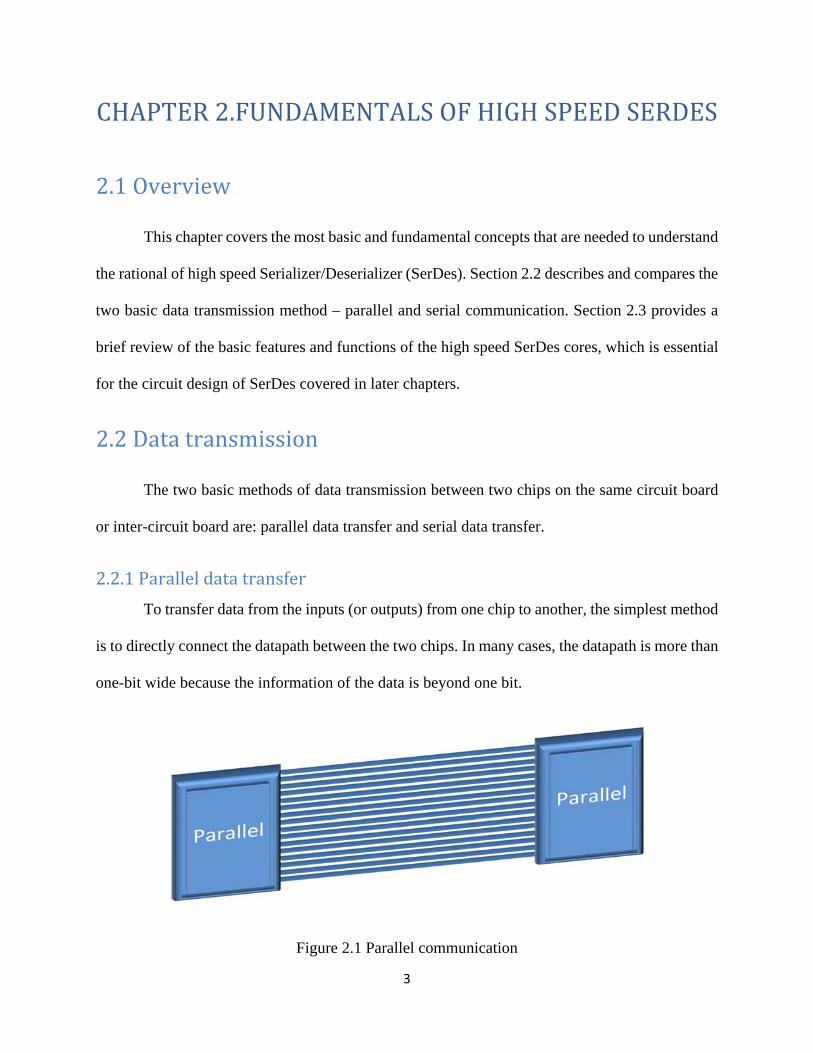
2.2.1Paralleldatatransfer
To transfer data from the inputs (or outputs) from one chip to another, the simplest method
is to directly connect the datapath between the two chips. In many cases, the datapath is more than
one-bit wide because the information of the data is beyond one bit.
Figure 2.1 Parallel communication

4
In figure 2.1, a simplified model of parallel data transfer is shown. Assuming there is an n-bit
datapath across the two chips A and B, an n-bit interconnect is needed in a parallel data bus.
The problems of parallel data transfer, however, includes: 1. Data skew, which could cause
serious problems like phase difference in modern high speed links due to high operating frequency.
2. Cross-talk, which refers to the interference between adjacent parallel data links. As the operating
frequency gets higher, the problem of cross-talk becomes more critical. 3. Multiple data links
consume board space. Extra pins associated with parallel links would lead to higher packaging
costs.
2.2.2Serialdatatransfer
The problems that are inherent to parallel data transfer as discussed in section 2.2.1 can be
eliminated with serial data transfer.
Figure 2.2 Serial communication
Serial data transfer requires much fewer data links, which reduces board space. Number of
I/O pins would significantly decrease and therefore lowers the packing costs. Data skew and cross-
talk problems would be much easier to solve in a serial data link.

5
2.3High‐speedSerDes
A device called Serializer/Deserializer (SerDes) allows data to transfer in a serial manner,
and is now playing a more and more important role in modern high speed applications. Such device
is capable of converting data from parallel to serial and vice versa, as is illustrated in a simplified
model in Figure 2.3.
Figure 2.3 Generic function of a SerDes
A basic block diagram showing the transmitter slice and receiver slice of a typical high
speed SerDes is presented in Figure 2.4. Firstly the n-bit parallel data is serialized in the transmitter
slice through a Serializer. An equalizer is then used to ensure good signal integrity of the serialized
data, which will then be driven into a differential signaling pair. On the receiver slice, a differential
receiver receives the serial data, which is then fed into a Clock Data Recovery (CDR) circuit. After
the recovery and equalization circuitries, the data is finally restored back to parallel data bus
through a Deserializer circuit on the receiver slice.

6
Figure 2.4 Basic block diagram of the transmitter and receiver slices of typical high speed Serdes
The following subsections provide generic descriptions of several circuits mentioned above
in more detail.
2.3.1Serializer/Deserializerblocks
The input to the serializer trasnsmit stage is an n-bit datapath, which is then serialized to a
one-bit serial data signal for application to the Feed Forward Equalizer (FFE) and driver stage.
The value of n is generally a multiple of 8 or 10, and may be programmable on some
implementations. Values of n which are multiples of 8 are useful for sending unencoded and/or
scrambled data bytes; values of n which are multiples of 10 are useful for protocols which use
8B/10B coding. The 8B/10B encoder is usually implemented by logic outside the SerDes core. [2]
The actual design of the datapath which is fed into the equalizer may be more than one bit
wide, and that results in more complex circuitries. However in general, the n-bit data input would
Channel
Channel
Serializer Equalizer Driver n
Receiver Recovery
and
Equalization
Driver n
Transmitter slice
Receiver slice

7
be serialized into an k-bit datapath, where n > k > 0. The k-bit data would be fed into the equalizer,
and further serialized at the driver stage if needed.
The deserializer block at the receiver slice, however, performs the inverse function of the
serializer at the transmitter slice. The serial data, after the Clock Data Recovery and Decision
Feedback Equalization block, is then deseralized back to an n-bit databus.
2.3.2Equalizer
A channel refers to the interconnect between the transmitter and receiver slice. It could
distort the serial data signal to varying extents in real world situations. If the signal rate is above
the cut-off frequency, then the high frequency components will get reduced therefore the signal is
distorted. To decode the signal properly, an equalizer is needed to restore the signal. Usually,
equalizers can be added to either the transmitter or the receiver side. In many existing SerDes
designs, a Feed Forward Equalizer (FFE) is adopted in the transmitter side while a Decision
Feedback Equalizer is needed in the receiver side. An FFE is normally implemented as a low-
frequency de-emphasis process to reduce low frequency signal envelope in proportion to the
attenuation experienced by the high-frequency pattern in the channel. A DFE is used in receiver
slice and plays an important role for signal integrity of the entire SerDes.
2.3.3Clockanddatarecovery(CDR)
In some modern digital data streams, especially high-speed serial data streams, strong
impairments and sever inter-symbol interference (ISI), which is due to frequency-dependent
channel loss, becomes a critical issue in high-speed interface design. ISI causes degradation of the
eye opening and timing jitter, and subsequent aggravations of bit error rate (BER) and signal
integrity of the entire system. [3] Since there is no exclusively allocated clock signal in high speed

8
SerDes transceivers, and a clock signal whose frequency is the baud rate and whose phase is
aligned to the data centers is indispensable for correct data recovery. Clock and Data Recovery
(CDR) circuitries monitor transitions and select optimal sampling phase for the data at midpoint
between edges. It extracts clock information from incoming data stream and uses this regenerated
clock to resample the data waveform and recover the data. CDR is a non-linear circuit and is an
important component to limit jitter, noise within the SerDes circuit. Practical microelectronic
implementation of CDR is a tradeoff among many design considerations. [4]
2.3.4Differentialdriverandreceiver
The differential driver stage is an analog circuit which drives the true and complement legs
of the differential signal. Output data must be driven such that jitter is minimized. Recall the
definition of jitter, which is the difference in time of when something was ideally to occur and
when it actually did occur. It is a signal timing deviation referenced to a recovered clock from the
recovered bit stream. Jitter is measured in unit intervals and captured visually with eye diagrams.
There are two types of jitter: Deterministic Jitter and Random Jitter. Jitter can cause inter-symbol
interference (ISI), which occurs if time required by signal to completely charge is longer than bit
interval. To ensure high signal integrity, jitter is ought to be minimized. Differential receiver stage
is an analog comparator circuit which compares the true and complement legs of the differential
signal and output a “0” or “1” logic signal based on the relative signal voltages. [2] [5]
2.3.5Phase‐lockedloop(PLL)
A Phase-locked loop (PLL) is a feedback system that generates an output signal whose
phase is related to the phase of an input reference signal. It is designed in such a way that the phase
error signal is reduced to zero. The phase-locked loop is basically a closed loop frequency

9
controlled system, which functioning is based on the phase sensitive detection of phase difference
between the input and output signals of the controlled oscillator. Figure 2.5 shows a classic
configuration of a PLL. The phase detector is a device that compares two input frequencies,
generating an output that is a measure of their phase difference. The phase detector produces an
output voltage that is proportional to the phase error, and the filtered output of the phase detector
is a dc signal, ant the control input to the voltage controlled oscillator (VCO) is a measure of the
input frequency. In some common designs of PLLs, a modulo-n counter is hooked between the
VCO output and phase detector, thus generating a multiple of the input reference frequency. [6]
Figure 2.5 A classic configuration of a Phase-locked loop (PLL)
PLL is a core component in a SerDes because it is an essential building block of Clock and
Data Recovery (CDR) circuits, and it reduces clock skew and jitter in high speed serial interfaces.
Phase Detector Loop Filter Voltage
Controlled
Oscillator
Divide by N
counter
Frequency
Reference
Input Frequency
Output
10
CHAPTER3.HIGHSPEEDSERDESARCHITECTUREANDDESIGN
3.1Overview
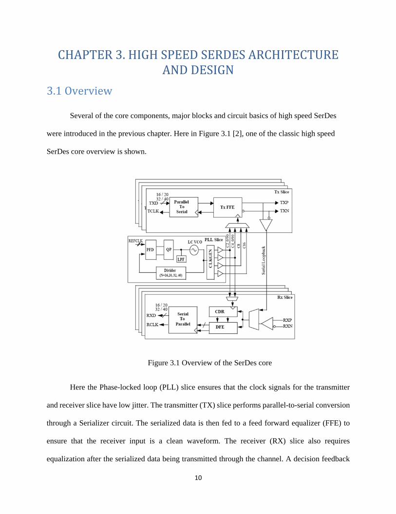
Several of the core components, major blocks and circuit basics of high speed SerDes
were introduced in the previous chapter. Here in Figure 3.1 [2], one of the classic high speed
SerDes core overview is shown.
Figure 3.1 Overview of the SerDes core
Here the Phase-locked loop (PLL) slice ensures that the clock signals for the transmitter
and receiver slice have low jitter. The transmitter (TX) slice performs parallel-to-serial conversion
through a Serializer circuit. The serialized data is then fed to a feed forward equalizer (FFE) to
ensure that the receiver input is a clean waveform. The receiver (RX) slice also requires
equalization after the serialized data being transmitted through the channel. A decision feedback

11
equalizer (DFE) is needed to improve the bit error rate (BER). After the signal is equalized, the
serial stream is driven through the Deseriazlier to perform the serial-to-parallel conversion. The
remainder of this chapter describes the design of Serializer in more detail.
3.2Serializer
Serializer operation performs the parallel-to-serial conversion as shown in Figure 3.1. A
simplified schematic of a 2:1 Serializer is presented here as an example. [Figure 3.2]
Figure 3.2 A 2:1 Serializer Circuit
Assuming the two bits of parallel data, Deven and Dood, are time-aligned into the Seralizer
and are synchronized to the half-rate C2 clock signal. The Parallel Deven and Dodd signals are
captured by the first two D-latches, which create the De and Do outputs on the rising edge of the
C2 clock signal. The Do’s signal is generated by resampling the Do signal on the falling edge of
the C2 clock signal. The select input of the 2:1 MUX is controlled by the C2 clock signal, so that
when the clock is low De input signal is selected, and when clock is high Do’s is selected.
D Q
D Q D Q
0 2:1 MUX
1
Deven
Dodd
C2clk
De
Do Do’
Serial Data
2:1 Serializer

12
3.2.1D‐latchdesign
A latch is an important component in the construction of several major blocks in high speed
SerDes, including the Serializer block, Differential Driver block, Phase Detector block,
Deserializer block, etc… A positive latch is a level sensitive circuit that passes the D input to the
Q output when the clock signal is high and it is said to be in the transparent mode. When the clock
is low, the input data sampled on the falling edge of the clock is held stable at the output for the
entire phase, and the latch is said to be in the hold mode. Similarly, a negative latch passes the D
input to the Q output when the clock signal is low. A register, however, is an edge-trigged
component contrary to the level-sensitive latches. A latch is an essential component in the
construction of an edge-triggered register. A flip-flop generally refers to any bistable component,
formed by the cross coupling of gates. Often in some textbooks, an edge-triggered register is
referred to as a flip-flop as well. [7]
Shown in Figure 3.1 is the transistor-level implementation of a positive MUX-based D-
latch built by using transmission gates.
Figure 3.2 A positive MUX-based D-latch using transmission gates

13
When the CLK signal is high, the bottom transmission gate is on, and the latch is
transparent – input signal D is copied to Q. During this time, the top transmission gate is off. When
the CLK signal is low, the bottom transmission gate is off while the top is on. The feedback ensures
the output is held as long as the CLK signal is low.
The problem of such MUX-based D-latch design using transmission gate is that it requires
both CLK and CLK_bar signal, which could lead to clock overlap and eventually cause race
condition to happen. A True Single Phase Clocked (TSPC) Latch [8] can overcome the problem
caused by clock overlap. Figure 3.2 shows the transistor implementation of a TSPC latch.
Figure 3.2 A True Single Phase Clocked Latch
For the positive TSPC latch shown above, when the CLK is high, the latch is in the
transparent mode, and corresponds to two cascaded inverters. When the CLK is low on the other
hand, both inverters are off and the latch is in hold mode.

14
A slightly different configuration of a TSPC with split out latch is used in the final design
of the Serializer as is shown in Figure 3.3. The advantage is that fewer transistors are needed in
this design, and thus lower power consumption of the overall system. Also smaller propagation
delay results in faster speed of the entire circuit. Again, no inverted clock signal is needed in this
design, so the circuit is free of clock skew issue.
Figure 3.3 A True Single Phase Clocked Latch with split output
3.2.2Multiplexerdesign
The transistor-level schematic of a transmission-gate multiplexer is shown in Figure 3.4.
The idea behind this circuit is to use two transmission-gates as simple switches to propagate either
input A or input B directly to the output. An extra inverter is needed to generate the inverted select
signal S_bar. While the upper transmission-gate is activated by S, the lower transmission-gate is
activated by S_bar, due to the wiring of their control inputs. When S is low, only the lower
transmission-gate is conducting (because S_bar is connected to its n-channel and S to its p-channel
transistor gate inputs), while the upper transmission-gate is non-conducting. As a result the value
of B is passed through to the output of the multiplexer. When S is high, the upper transmission-

15
gate is activated, while the lower transmission-gate is non-conducting. Therefore the value of A is
passed through to the multiplexer output.
Figure 3.4 Transmission-gate multiplexer
However, traditional transistor sizing method and logical effort cannot be applied to this
transmission-gate multiplexer deisgn, and thus it is hard to find out the optimal transistor size for
maximum speed theoretically. Also, in order to lower the equivalent resistance Req, the
transmission gate must be made wide. The capacitance of the gates, however, will also be
increased, resulting in no reduction in the time constant of the transmission-gate multiplexer. As
a result, another design called Current Mode Logic (CML) Multiplexer is adopted and is shown in
Figure 3.5. The CML circuits are widely used in GHz range high speed bipolor driver or
multiplexer implementations.
The differential select signals, S and S_bar, select which of the two data-input A and B to
be connected to the output. When the select signal S is high (and S_bar is low), A directly affect
the output while B is disconnected. When the select signal S goes low (and S_bar high) B will be
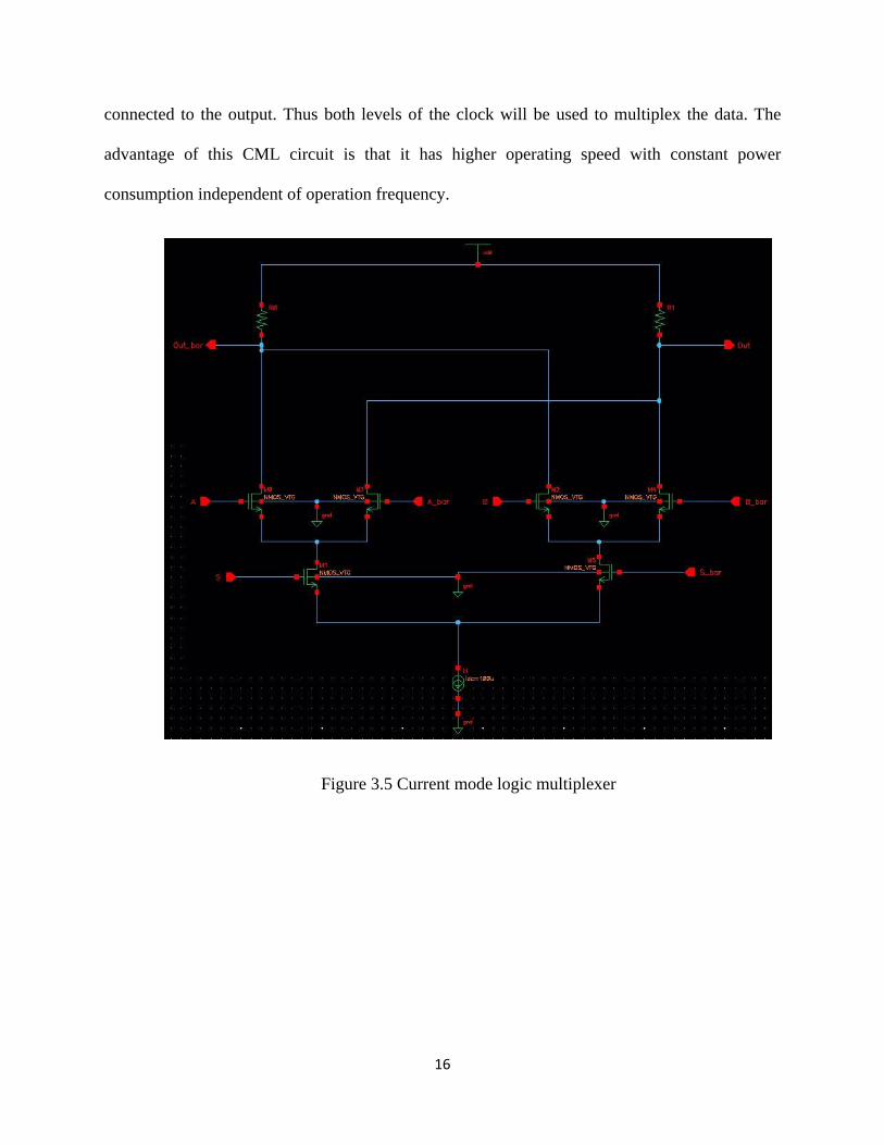
16
connected to the output. Thus both levels of the clock will be used to multiplex the data. The
advantage of this CML circuit is that it has higher operating speed with constant power
consumption independent of operation frequency.
Figure 3.5 Current mode logic multiplexer

17
CHAPTER4.SERDESCIRCUITDESIGNTUTORIAL
4.1Overview
In this chapter a 2:1 Serializer topology in a schematic is created step by step using Cadence
Virtuoso IC 6.1.5. This 2:1 Serializer circuit serves as an example which helps one to understand
the serialization operation. The step by step tutorial is meant to be written in a way such that any
circuit designer with no EDA tools experience can easily follow.
4.2SchematicEditor
4.2.1Creatinglibrary
1. Create a new library. This is done by clicking File New Library, as is shown in Figure
4.1. There will be a new window where one may create a “library” by filling in a name. In
Cadence, a library is essentially a directory in the user’s home account containing all the
project files.
Figure 4.1: New library

18
2. Specify a library name. In this case, for example, the library is named as “D-latch_Demo”.
Figure 4.2: Name the library and choose technology file
3. Once the name of the new library is filled in, choose “Attach Library to an existing
technology” in the Technology File section as is in Figure 4.2. From the technology library
list, select “NCSU_TechLib_FreePDK45”, which corresponds to a NCSU 45 nanometer
technology, then click “OK”. [Figure 4.3]
Figure 4.3: Attach library to technology file
4. A new library called “D-latch_Demo” is now created and can be found in the Library
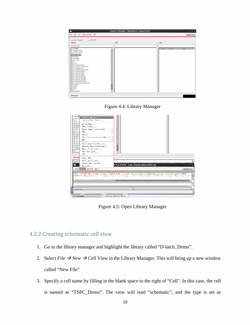
Manager [Figure 4.4]. If the Library Manager is not shown, one can click Tools and select
Library Manager. [Figure 4.5]
19
Figure 4.4: Library Manager
Figure 4.5: Open Library Manager
4.2.2Creatingschematiccellview
1. Go to the library manager and highlight the library called “D-latch_Demo”.
2. Select File New Cell View in the Library Manager. This will bring up a new window
called “New File”
3. Specify a cell name by filling in the blank space to the right of “Cell". In this case, the cell
is named as “TSPC_Demo”. The view will read “schematic”, and the type is set as

20
“schematic”. Note that the “Application” is automatically set to “Schematics L” as is in
Figure 4.6. Then press “OK”, which brings a new window, “Virtuoso Schematic Editor L”.
A blank schematic editing window should be shown as in Figure 4.7.
Figure 4.6: Create new cell view
Figure 4.7: Virtuoso Schematic Editor

21
4.2.3Instantiatingsymbols
1. To add new components, select Create Instance in the Virtuoso Schematic Editor.
Alternatively, this can be done by clicking the button Instance on the tool bar, as is
shown in Figure 4.8.
Figure 4.8: Create Instance
2. In the Add Instance window, click “Browse”, which will bring up a new window called
“Library Browser – Add Instance”. Choose “NCSU_Devices_FreePDK45” on the library
list, and select the part needed. Make sure to select the “View”, “Symbol” as is shown in
Figure 4.9. If needed, fill in the proper values for the specific design.

22
Figure 4.9: Add Instance
In this design, a TSPC D-latch with split output will be implemented.
3. Once the component has been selected, place it in the Virtuoso Schematic Editor window.
This can be done by selecting the part (in this case, “PMOS_VTG”), and then a PMOS
symbol will be attached to the cursor. Left click to place that symbol on the Virtuoso
Schematic Editor window. See Figure 4.10.
After a particular component has been properly placed, strike the “Esc” key to finish.

23
Figure 4.10: Placing components
4. To size the transistor, right click the instance (PMOS_VTG or NMOS_VTG), and choose
“Properties”, or alternatively, click the instance and click Edit Properties Objects. In
the pop up window called “Edit Object Properties” as shown in Figure 4.11, change the
value of the transistor size.

24
Figure 4.11: Transistor sizing
5. To connect components with wires, select Create Wire (narrow), or alternatively click
the button “Create Narrow Wire” on the tool bar. Left click the mouse to attach on end
of the wire to a node of one component, and then the wire can be routed to the other
component and attached in, as is shown in Figure 4.12. Strike the “Esc” key to terminate
this operation.
Figure 4.12 Connecting Components

25
6. To move objects, select Edit Move, then center the cursor over the object until a
rectangle with sides appears. Left click to get a copy of the object, then move the object to
any point in the schematic. Once the object is located to the proper place, strike the “Esc”
key and the object will be deposited at that location.
7. Repeat step 1 to add another NMOS and PMOS components, or alternatively, copy from
the previously instantiated components. To copy, select Edit Copy in the top menu, left
click the component and move the yellow copy to another point.
8. To add pins, select Create Pin, or alternatively click the button Pin . [Figure 4.13]
Figure 4.13 Create Pins
In the pop up window called “Add Pin”, specify Pin Names and Direction (input, output,
etc…) from the dropdown list, as shown in Figure 4.14.

26
Figure 4.14 Pin names and direction
9. To place power supply and ground symbols, go to Add Instance and choose the library
“NCSU_Analog_Parts”. In this case, use “vdd” for power supply symbols and use “gnd”
for ground symbols. [Figure 4.15]
Figure 4.14 Power supply and ground

27
10. When schematic editing is finished, click File Check and save, or alternatively click the
button Check and save . If any error or warning message appears, refer to the log
window as is shown in Figure 4.15.
Figure 4.15 Log window
To zoom the schematic that fits the full window, click the button Zoom to fit . The
complete TSPC D-latch is shown in Figure 4.16.
Figure 4.16 Schematic of the TSPC D-latch

28
11. To create a symbol from the schematic, choose Create Cellview From Cellview, and
a pop up window called “Cellview From Cellview” will appear as is shown in Figure 4.17.
Within the symbol, it contains the whole schematic of the TSPC D-latch.
Figure 4.17 Create a symbol from schematic
12. After clicking “OK”, a new window that shows the symbol of the D-latch will pop up, as
is shown in Figure 4.18.
Figure 4.18 Symbol of the TSPC D-latch

29
One can also change the name of the symbol by left click the name [@partName], then
click the button Edit Properties , and change the name on the Edit properties window.
To change the shape of the symbol, use the tools shown in Figure 4.19
Figure 4.19 Tools to edit symbol
13. Check and save . Now the symbol of the TSPC D-latch has successfully been created,
and it should be shown under the view list of the TSPC D-latch along with the schematic,
in the Library Manager.
Figure 4.20 Symbol and schematic
4.2.4Creatingtestbench
Once all the symbols have created, a test bench is needed to place all the symbols together in
one single schematic, connect them together using wires, and run simulations.
1. To create a test bench, choose File New Cell View. In the pop up window, specify
the cell name. In this case, this cell is named as “Demo”. Note that this cell is created in a
separate library called “2-1Serializer_Demo” as is shown in Figure 4.21.
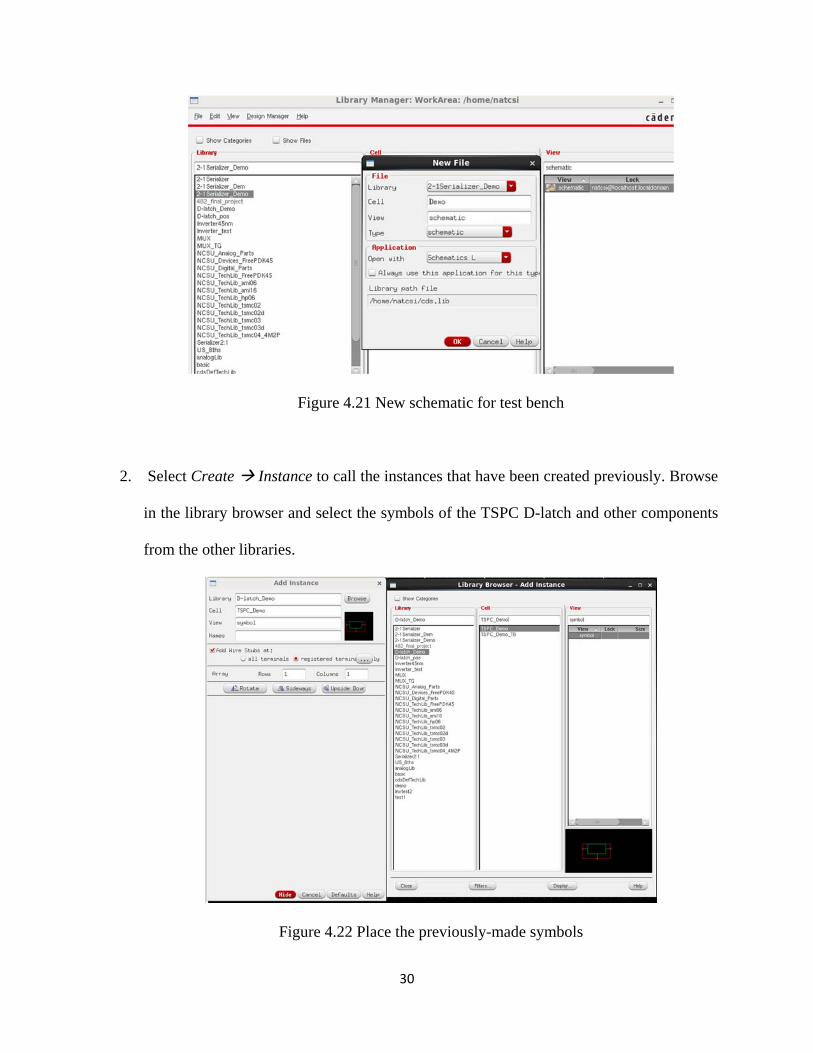
30
Figure 4.21 New schematic for test bench
2. Select Create Instance to call the instances that have been created previously. Browse
in the library browser and select the symbols of the TSPC D-latch and other components
from the other libraries.
Figure 4.22 Place the previously-made symbols

31
3. Connect all the symbols using wires, and create pins to the circuit as is shown in Figure
4.23.
Figure 4.23 2:1 Serializer circuit
4. To further simply the test bench, combine everything into one single symbol by choosing
Create Cellview From cellview, and a single symbol containing the whole 2:1
Serializer circuit has been created as shown in Figure 4.24.
Figure 4.24 Symbol of the entire 2:1 Serializer circuit

32
5. Create a new schematic as the test bench for the 2:1 Serializer circuit.
6. Create Instance, choose “NCSU_Analog_Parts”, select “cap” for capacitor, and place
it on the test bench. Connect one end of the capacitor to the “Serial” output of the 2:1
serializer.
7. For signal sources, go to Create Instance, select “vpulse” from “NCSU_Analog_Parts”
and place it on the test bench. Edit object properties, as is shown in Figure 4.25. Click
“OK” after changing the values in the pop up window. Connect the signal sources to the
inputs of the 2:1 Serializer circuit.
Figure 4.25 Edit properties of signal sources

33
8. Place the power supply by selecting Create Instance, browse library and choose “vdc”
from the “NCSU_Analog_Parts”. Change the DC voltage to 1.2V before placing it to the
test bench. Connect wires to the positive and negative nodes and leave them floating. Click
the button Create Wire Name , type in “vdd!” for the name in the pop up window, and
then move the cursor to the floating wire connecting to the positive node of “vdc” and left
click to place the name to the wire. Now the wire connecting to the positive node of “vdc”
is connecting to all “vdd” nodes in all the symbols contained inside the 2:1 serializer circuit.
Add wire name “gnd!” to the wire connecting to the negative node of “vdc” so that all the
nodes named as “gnd” are now connected to the negative node of “vdc”. [Figure 4.28]
Figure 4.28 Place the power supply and add wire names
9. The complete test bench for the 2:1 Serializer circuit is shown in Figure 4.29.

34
Figure 4.29 Test bench for the 2:1 Serializer circuit
4.2.5ExtractingHSPICENetlist
1. To extract the netlist of the schematic for HSPICE simulation, select Launch ADE L to
open Virtuoso Analog Design Environment L. [Figure 4.30]
Figure 4.30 Launch Virtuoso Analog Design Environment

35
2. A pop up window called Virtuoso Analog Design Environment should appear. Choose
Setup Simulatior/Directory/Host… as is shown in Figure 4.31
Figure 4.31 Setup simulator in the ADE L
3. In the pop up window called “Choosing Simulator/Directory/Host”, selector “hspiceD”
from the dropdown list. [Figure 4.32]
Figure 4.32 Choosing simulator
36
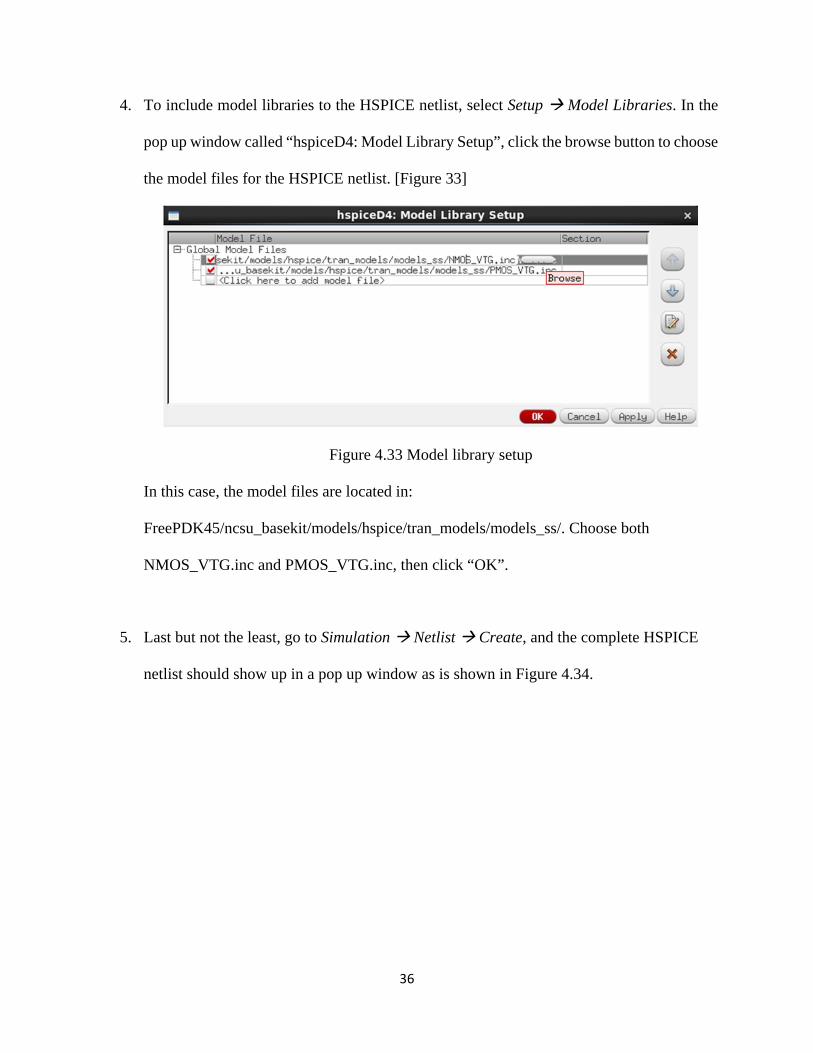
4. To include model libraries to the HSPICE netlist, select Setup Model Libraries. In the
pop up window called “hspiceD4: Model Library Setup”, click the browse button to choose
the model files for the HSPICE netlist. [Figure 33]
Figure 4.33 Model library setup
In this case, the model files are located in:
FreePDK45/ncsu_basekit/models/hspice/tran_models/models_ss/. Choose both
NMOS_VTG.inc and PMOS_VTG.inc, then click “OK”.
5. Last but not the least, go to Simulation Netlist Create, and the complete HSPICE
netlist should show up in a pop up window as is shown in Figure 4.34.
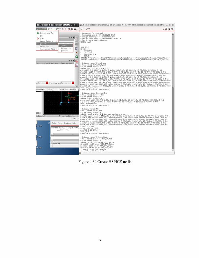
37
Figure 4.34 Create HSPICE netlist

38
CHAPTER5.HSPICEMEASUREMENTSANDANALYSIS
5.1OverviewIn this chapter, the 2:1 Serializer circuit designed in Chapter 4 is simulated HSPICE.
Several measurements and analysis are performed after the simulation process and the results are
shown in cscope.
5.2HSPICESimulationOnce the HSPICE netlist has been successfully extracted, simulation process could be
performed by the following steps:
1. Open up a text editor (such as genit or xemacs) and enter the netlist extracted from the
schematic. Save it to the work directory with a file name extension of .cir. In this case, it
is named as 2-1Serializer_HSPICE.cir
2. In the Linux terminal, change to the directory where the HSPICE netlist is located.
3. To run HSPICE simulation, use the following command in the Linux terminal: hspice 2-
1Serializer_HSPICE.cir
After the HSPICE simulation run, four result files are created. The “2-
1Serializer_HSPICE.ic0” file is the text file which contains the circuit initial conditions. The “2-
1Serializer_HSPICE.st0” file is the text file which contains a summary of the simulation. The “2-
1Serializer_HSPICE.sw0” file is the binary file which contains the cd sweep waveforms for the
voltage transfer characteristic plot. The “2-1Serializer_HSPICE.tr0” is the binary file which
contains the transient analysis waveforms.
5.3MeasurementandanalysisTo perform further measurement and analysis of the results of the simulation, the tool
CosmosScope is used in this section. Use the command in the Linux terminal: Cscope. Go to File
Open Plotfiles to view and analyze the results.
The timing diagram of the 2:1 Serializer is shown in Figure 5.1. The behavior of the 2:1
Serializer matches the expectation. When C2clk signal (the first waveform from top) is low, output
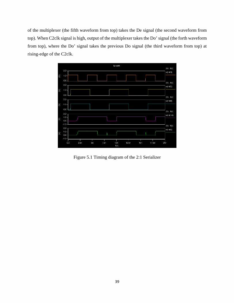
39
of the multiplexer (the fifth waveform from top) takes the De signal (the second waveform from
top). When C2clk signal is high, output of the multiplexer takes the Do’ signal (the forth waveform
from top), where the Do’ signal takes the previous Do signal (the third waveform from top) at
rising-edge of the C2clk.
Figure 5.1 Timing diagram of the 2:1 Serializer

40
CHAPTER6.CONCLUTIONANDFUTUREWORK
In summary, the work presented in this thesis laid down a path necessary to gain knowledge
of designing and building analog and digital circuits. A simple Serializer circuit is designed,
created and simulated using Cadence Virtuoso and HSPICE. The step-by-step “cookbook style”
tutorial of mixed-signal circuit design and simulation was shown, and could be applied to other
transistor level circuit design projects as well. The Serializer circuit presented in this thesis is not
only a key component in a SerDes system, but also serves as an example for one to understand the
serialization process. Other core components of a SerDes, including Deserializer block, Equalizers,
Clock and Data Recovery (CDR), Differential driver and receiver, and Phase-locked loop (PLL)
were also discussed.
The next step for this project is to finish all the other core components of the SerDes as
discussed earlier. The interconnection between each component would be the following step, and
eventually all major blocks would be integrated as one entire SerDes system, which functions
properly at the desired frequency. Meanwhile, alternative designs or topologies for any sub-circuits
such as D-latches, multiplexers, voltage controlled oscillator (VCO) is being explored and could
be replaced to our existing designs if the overall system speed is found to be increased.
Furthermore, transistor sizing and optimization are needed so as to increase the operating
frequency of the entire SerDes and minimize the propagation delay and power consumption.
Finally, signal and power integrity analysis would be done on the entire SerDes in order to find
out means to reduce the unwanted effects such as cross-talk and jitter/phase noise.

41
References
[1]LatticeSemiconductorCorporation,"SerdesIntroduction,"ChinaDistributorFAETraining,January2003.
[2]D.Stauffer,J.Mechler,K.Dramstad,C.Ogilvie,A.Mohammad,J.RockrohrandM.Sorna,HighSpeedSerdesDevicesandApplications,NewYork:Springer,2008.
[3]Y.Shim,W.Lee,E.Song,J.ChoandJ.Kim,"ACompactandWide‐BandPassiveEqualizerDesign,"IEEEMICROWAVEANDWIRELESSCOMPONENTSLETTERS,vol.20,no.5,pp.256‐258,May2010.
[4]D.Chen,"SerDesTransceiversforHigh‐speedSerialCommunications,"CarletonUniversity,Ottawa,Jan2008.
[5]J.Schutt‐Ainé,"SignalIntegrity,"ClassnotesforECE451,DepartmentofElectricalandComputerEngineering,UniversityofIllinoisatUrbana‐Champaign,2009.
[6]T.VanRoon,"PLLTutorial,"19October2010.[Online].Available:http://www.sentex.ca/~mec1995/gadgets/pll/pll.html.[Accessed30June2013].
[7]J.Rabaey,A.ChandrakasanandB.Nikolic,DigitalIntegratedCircuits:ADesignPerspective,PrenticeHall,2003.
[8]J.YuanandC.Svensson,"High‐SpeedCMOSCircuitTechnique,"IEEEJournalofSolid‐StateCircuits,vol.24,no.1,pp.62‐70,1989.