Embed Size (px)
Citation preview
Bitte decken Sie die schraffierte Fläche mit einem Bild ab.
Please cover the shaded area with a picture.
(24,4 x 11,0 cm)
TIE Plus. The step towards interconnect simulation technology Catalin Negrea, Ph. D. Team Leader - EE Simulation & Controller Platforms
Technical Expert - Signal & Power Integrity
Continental Automotive, Interior Division 23 April 2015 IID EE CDH
Public
IID EE HW
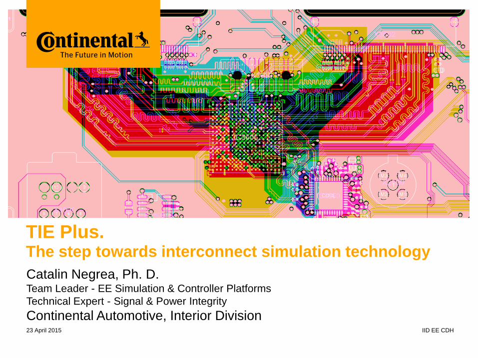
Virtual Prototyping
2
SPICE-like
Circuit Sim.
› Virtual prototyping = the usage of computer based modeling and simulation techniques
for the definition of a multidisciplinary model of the device under development (with the
goal of predicting physical behavior in different use cases)
CAD Model
Thermal
Simulation
Virtual
Prototype
Source: Aberdeen Group Market Study “Why PCB Design
Matters to the Executive”, Feb. 2010
SI \ PI \ EMI
Simulation
Get it right the first time !
Reduce number of design loops,
prototype costs, development time
› “Ideal world” goal
› “Real R&D world” goal
Public
IID EE HW
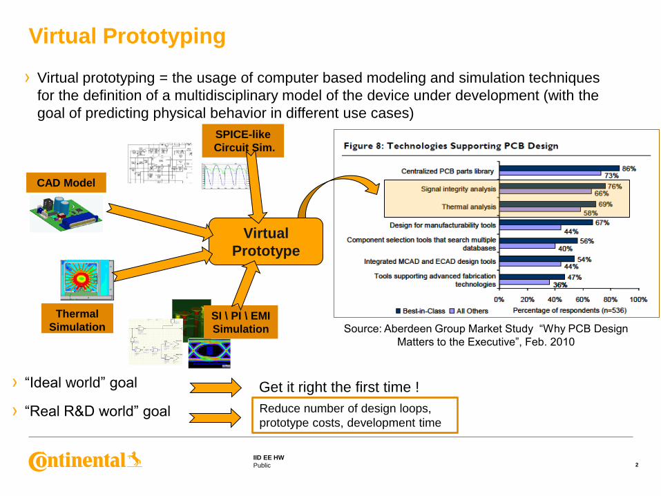
TIE Plus Objectives
3
› TIE Plus = a new contest challenge under the TIE brand, dedicated to virtual
prototyping disciplines that support high-complexity PCB design
› Objectives:
Promoting simulation based PCB design disciplines in universities and
R&D centers
Stimulating the development of future specialist in the field of interconnect
simulation in a accordance to best-in-class companies demands
Create a collaborative-competitive environment where the candidates
presents their technical solutions, but also exchange ideas on simulation
approaches and get in touch other PCB design professionals
› Subject topics for upcoming editions of TIE plus:
Signal Integrity (SI) -> simulations for signal integrity associated with
wired data transmissions at PCB and system level
Power Integrity (PI) -> simulation power supply distribution networks in
high frequency digital applications
Public
IID EE HW
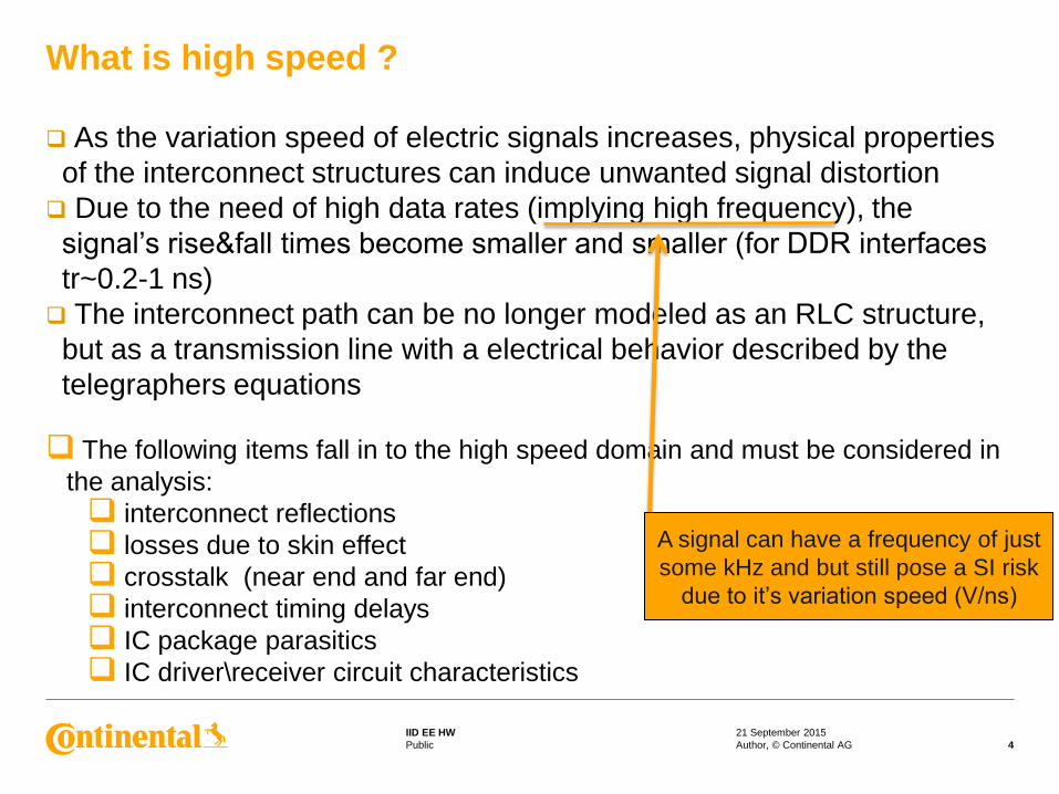
As the variation speed of electric signals increases, physical properties
of the interconnect structures can induce unwanted signal distortion
Due to the need of high data rates (implying high frequency), the
signal’s rise&fall times become smaller and smaller (for DDR interfaces
tr~0.2-1 ns)
The interconnect path can be no longer modeled as an RLC structure,
but as a transmission line with a electrical behavior described by the
telegraphers equations
The following items fall in to the high speed domain and must be considered in
the analysis:
interconnect reflections
losses due to skin effect
crosstalk (near end and far end)
interconnect timing delays
IC package parasitics
IC driver\receiver circuit characteristics
What is high speed ?
21 September 2015
4 Author, © Continental AG
A signal can have a frequency of just
some kHz and but still pose a SI risk
due to it’s variation speed (V/ns)
Public
IID EE HW
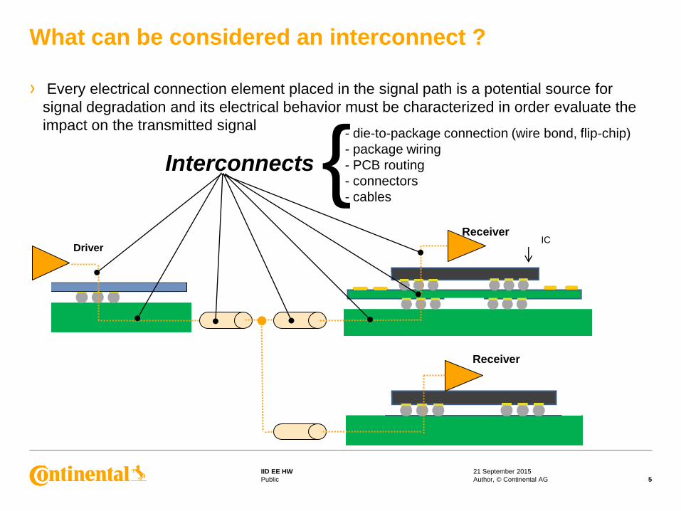
› Every electrical connection element placed in the signal path is a potential source for
signal degradation and its electrical behavior must be characterized in order evaluate the
impact on the transmitted signal
What can be considered an interconnect ?
21 September 2015
5 Author, © Continental AG
Interconnects
IC Driver
Receiver
Receiver
- die-to-package connection (wire bond, flip-chip)
- package wiring
- PCB routing
- connectors
- cables
Public
IID EE HW
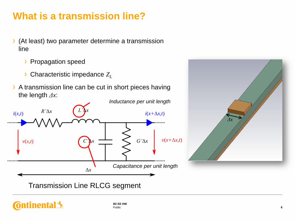
What is a transmission line?
6
› (At least) two parameter determine a transmission
line
› Propagation speed
› Characteristic impedance ZL
› A transmission line can be cut in short pieces having
the length Δx:
Δx
v(x,t) v(x+Δx,t)
i(x,t) i(x+Δx,t) R’Δx L’Δx
C’Δx G’Δx
Δx
Inductance per unit length
Capacitance per unit length
Transmission Line RLCG segment
Public
IID EE HW
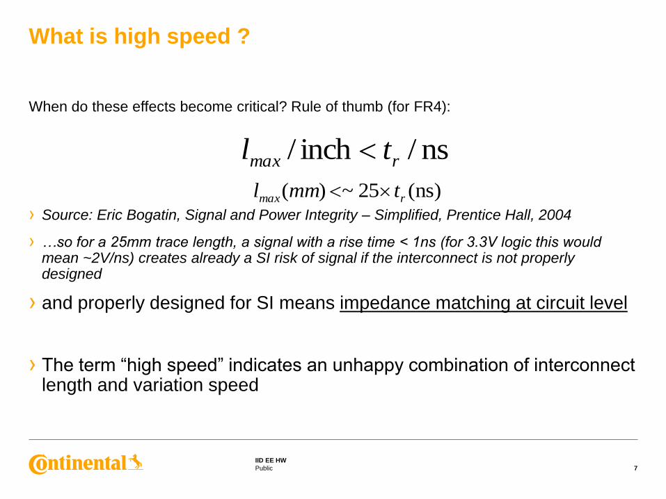
When do these effects become critical? Rule of thumb (for FR4):
› Source: Eric Bogatin, Signal and Power Integrity – Simplified, Prentice Hall, 2004
› …so for a 25mm trace length, a signal with a rise time < 1ns (for 3.3V logic this would mean ~2V/ns) creates already a SI risk of signal if the interconnect is not properly designed
› and properly designed for SI means impedance matching at circuit level
› The term “high speed” indicates an unhappy combination of interconnect length and variation speed
What is high speed ?
7
ns/inch/ rmax tl
ns)(25~)( rmax tmml
Public
IID EE HW
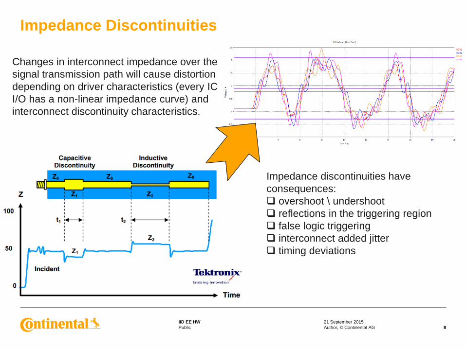
Impedance Discontinuities
21 September 2015
8 Author, © Continental AG
Impedance discontinuities have
consequences:
overshoot \ undershoot
reflections in the triggering region
false logic triggering
interconnect added jitter
timing deviations
Changes in interconnect impedance over the
signal transmission path will cause distortion
depending on driver characteristics (every IC
I/O has a non-linear impedance curve) and
interconnect discontinuity characteristics.
Public
IID EE HW
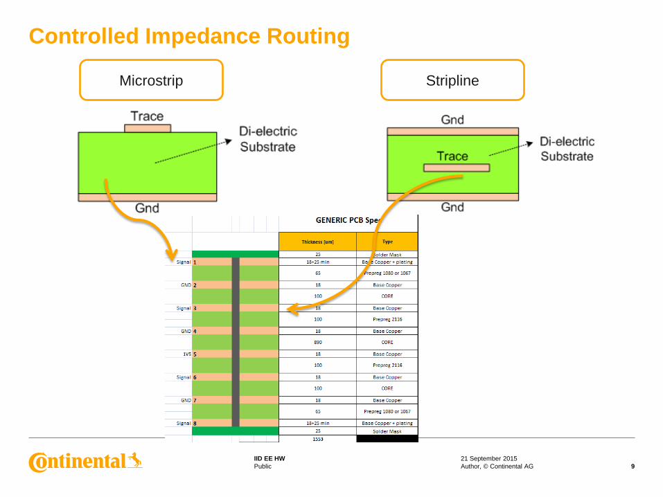
Controlled Impedance Routing
21 September 2015
9 Author, © Continental AG
Stripline Microstrip
Public
IID EE HW
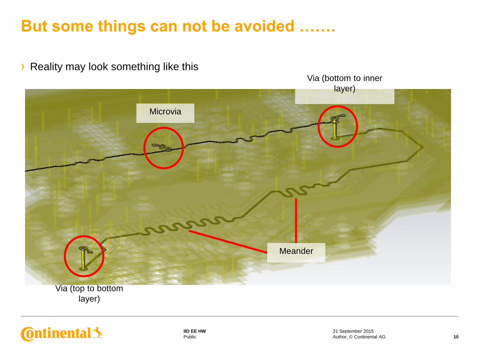
But some things can not be avoided …….
21 September 2015
10 Author, © Continental AG
› Reality may look something like this
Via (top to bottom
layer)
Via (bottom to inner
layer)
Microvia
Meander
Public
IID EE HW
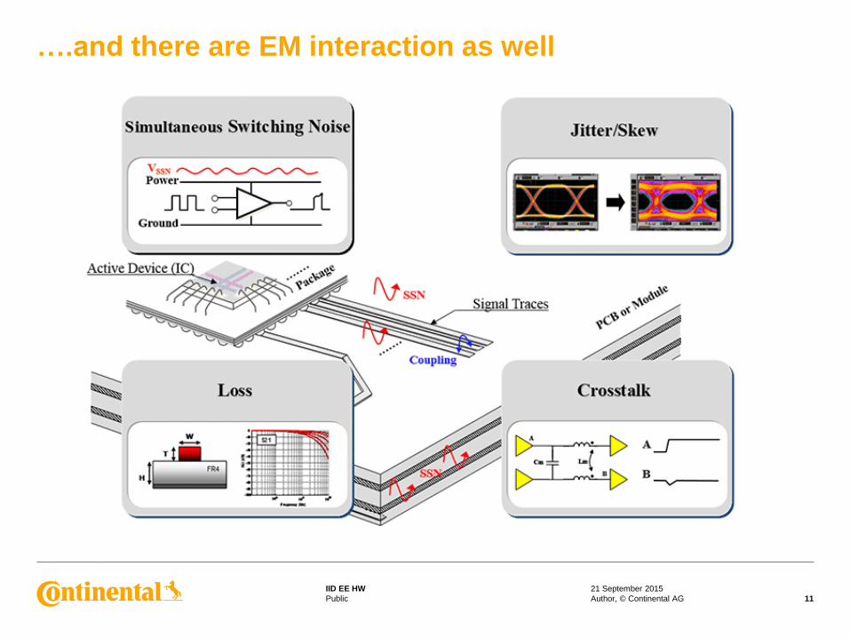
….and there are EM interaction as well
21 September 2015
11 Author, © Continental AG
Public
IID EE HW
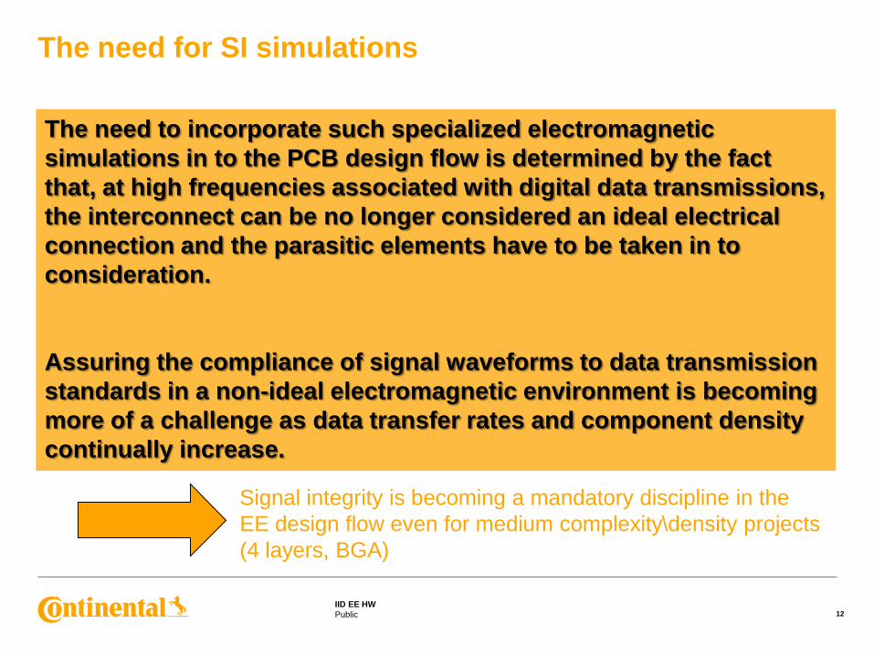
The need for SI simulations
12
The need to incorporate such specialized electromagnetic
simulations in to the PCB design flow is determined by the fact
that, at high frequencies associated with digital data transmissions,
the interconnect can be no longer considered an ideal electrical
connection and the parasitic elements have to be taken in to
consideration.
Assuring the compliance of signal waveforms to data transmission
standards in a non-ideal electromagnetic environment is becoming
more of a challenge as data transfer rates and component density
continually increase.
Signal integrity is becoming a mandatory discipline in the
EE design flow even for medium complexity\density projects
(4 layers, BGA)
Public
IID EE HW
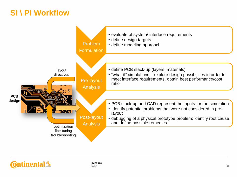
SI \ PI Workflow
13
Problem
Formulation
• evaluate of system\ interface requirements
• define design targets
• define modeling approach
Pre-layout
Analysis
• define PCB stack-up (layers, materials)
• “what-if” simulations – explore design possibilities in order to meet interface requirements, obtain best performance/cost ratio
Post-layout
Analysis
• PCB stack-up and CAD represent the inputs for the simulation
• Identify potential problems that were not considered in pre-layout
• debugging of a physical prototype problem; identify root cause and define possible remedies
optimization
fine-tuning
troubleshooting
layout
directives
PCB
design
Public
IID EE HW
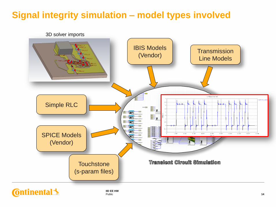
Signal integrity simulation – model types involved
14
IBIS Models
(Vendor)
SPICE Models
(Vendor)
Simple RLC
Transmission
Line Models
Touchstone
(s-param files)
3D solver imports
Public
IID EE HW
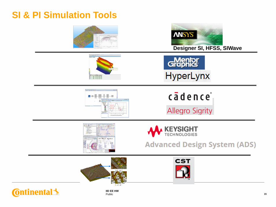
SI & PI Simulation Tools
15
Designer SI, HFSS, SIWave
Public
IID EE HW
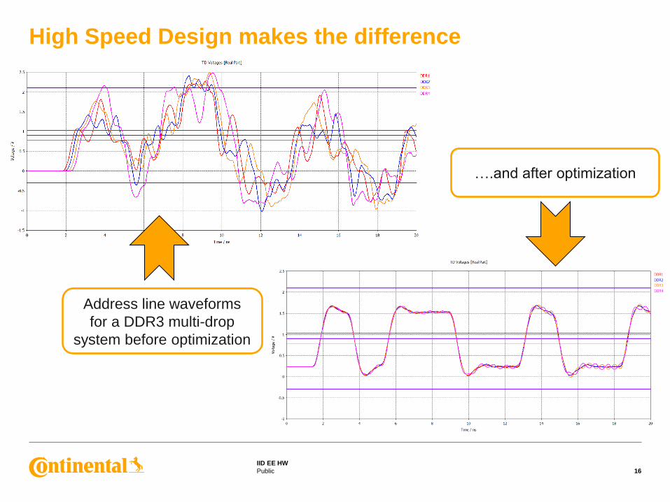
High Speed Design makes the difference
16
Address line waveforms
for a DDR3 multi-drop
system before optimization
….and after optimization
Public
IID EE HW
Power Integrity
21 September 2015
17 Author, © Continental AG
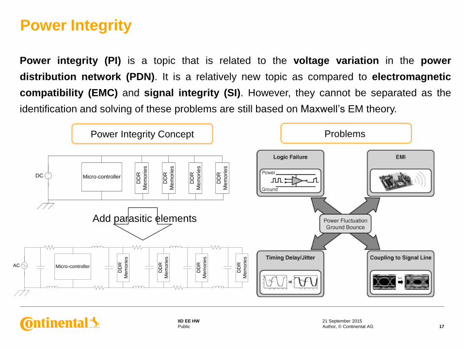
Power integrity (PI) is a topic that is related to the voltage variation in the power
distribution network (PDN). It is a relatively new topic as compared to electromagnetic
compatibility (EMC) and signal integrity (SI). However, they cannot be separated as the
identification and solving of these problems are still based on Maxwell’s EM theory.
Problems Power Integrity Concept
Micro-controller
DD
R
Me
mo
rie
s
DD
R
Me
mo
rie
s
DD
R
Me
mo
rie
s
DD
R
Me
mo
rie
s
DC
Micro-controller
DD
R
Me
mo
rie
s
DD
R
Me
mo
rie
s
DD
R
Me
mo
rie
s
DD
R
Me
mo
rie
s
AC
Add parasitic elements
Public
IID EE HW
Power Integrity
18
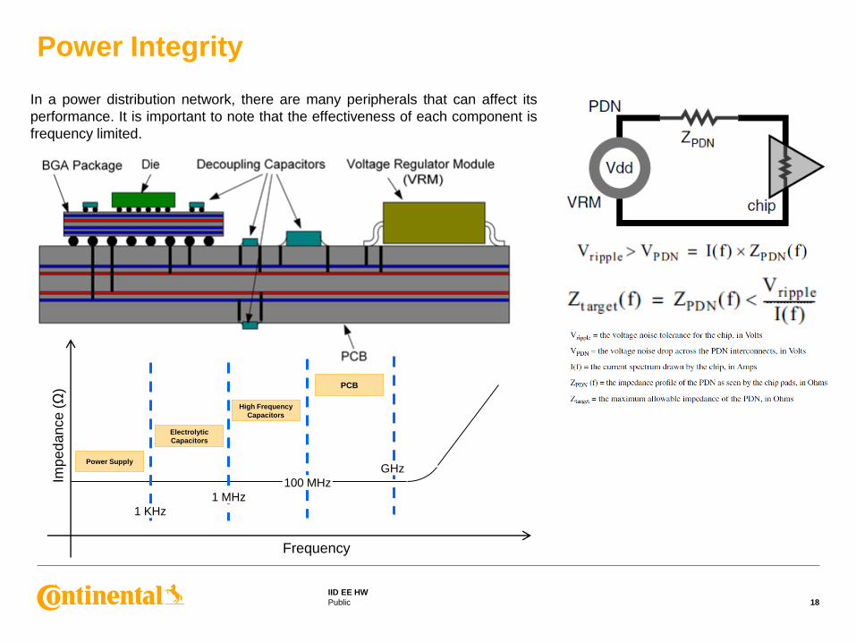
In a power distribution network, there are many peripherals that can affect its
performance. It is important to note that the effectiveness of each component is
frequency limited.
Imp
ed
ance
(Ω
)
Frequency
1 KHz
Power Supply
1 MHz
Electrolytic
Capacitors
High Frequency
Capacitors
100 MHz
GHz
PCB
Public
IID EE HW
TIE Plus workflow
19
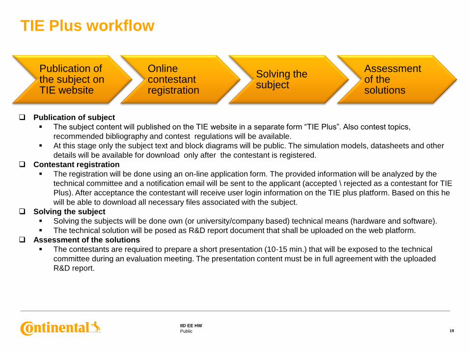
Publication of the subject on TIE website
Online contestant registration
Solving the subject
Assessment of the solutions
Publication of subject
The subject content will published on the TIE website in a separate form “TIE Plus”. Also contest topics,
recommended bibliography and contest regulations will be available.
At this stage only the subject text and block diagrams will be public. The simulation models, datasheets and other
details will be available for download only after the contestant is registered.
Contestant registration
The registration will be done using an on-line application form. The provided information will be analyzed by the
technical committee and a notification email will be sent to the applicant (accepted \ rejected as a contestant for TIE
Plus). After acceptance the contestant will receive user login information on the TIE plus platform. Based on this he
will be able to download all necessary files associated with the subject.
Solving the subject
Solving the subjects will be done own (or university/company based) technical means (hardware and software).
The technical solution will be posed as R&D report document that shall be uploaded on the web platform.
Assessment of the solutions
The contestants are required to prepare a short presentation (10-15 min.) that will be exposed to the technical
committee during an evaluation meeting. The presentation content must be in full agreement with the uploaded
R&D report.
Public
IID EE HW
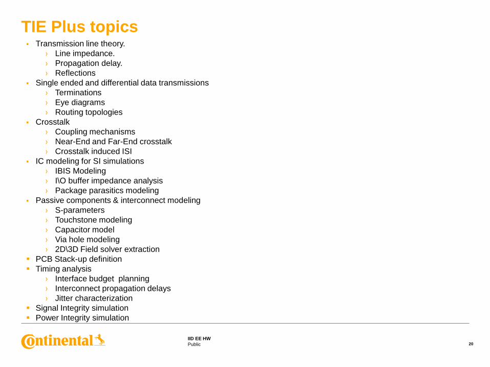
TIE Plus topics
20
Transmission line theory.
› Line impedance.
› Propagation delay.
› Reflections
Single ended and differential data transmissions
› Terminations
› Eye diagrams
› Routing topologies
Crosstalk
› Coupling mechanisms
› Near-End and Far-End crosstalk
› Crosstalk induced ISI
IC modeling for SI simulations
› IBIS Modeling
› I\O buffer impedance analysis
› Package parasitics modeling
Passive components & interconnect modeling
› S-parameters
› Touchstone modeling
› Capacitor model
› Via hole modeling
› 2D\3D Field solver extraction
PCB Stack-up definition
Timing analysis
› Interface budget planning
› Interconnect propagation delays
› Jitter characterization
Signal Integrity simulation
Power Integrity simulation
Public
IID EE HW
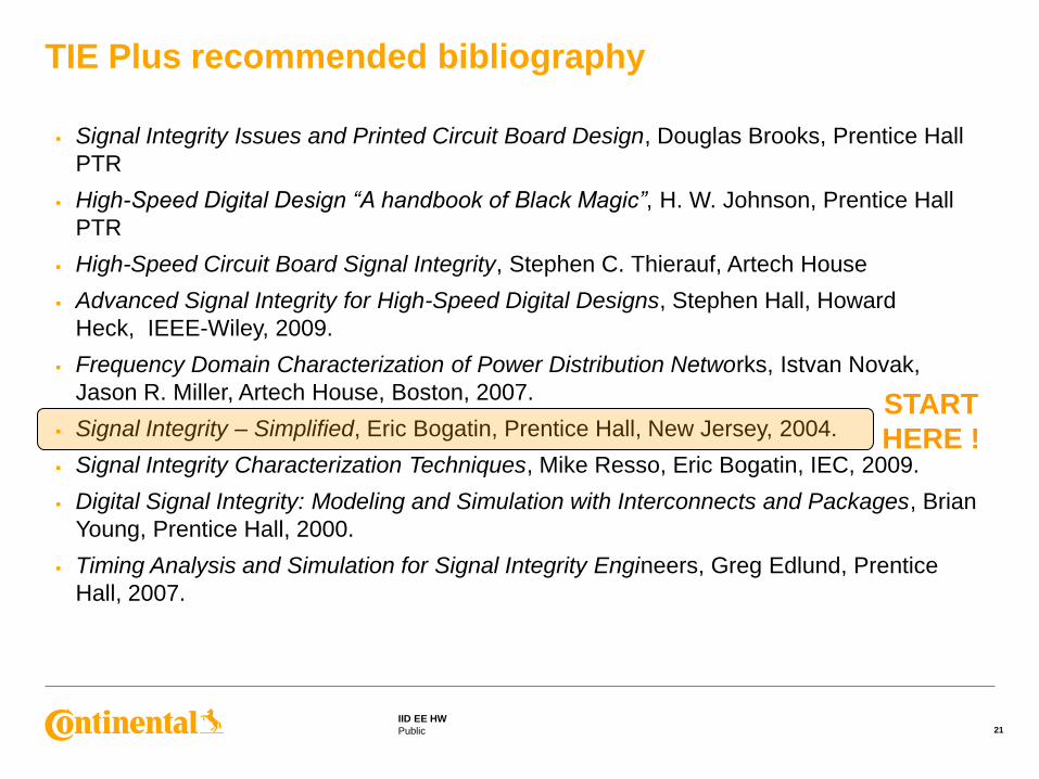
TIE Plus recommended bibliography
21
Signal Integrity Issues and Printed Circuit Board Design, Douglas Brooks, Prentice Hall
PTR
High-Speed Digital Design “A handbook of Black Magic”, H. W. Johnson, Prentice Hall
PTR
High-Speed Circuit Board Signal Integrity, Stephen C. Thierauf, Artech House
Advanced Signal Integrity for High-Speed Digital Designs, Stephen Hall, Howard
Heck, IEEE-Wiley, 2009.
Frequency Domain Characterization of Power Distribution Networks, Istvan Novak,
Jason R. Miller, Artech House, Boston, 2007.
Signal Integrity – Simplified, Eric Bogatin, Prentice Hall, New Jersey, 2004.
Signal Integrity Characterization Techniques, Mike Resso, Eric Bogatin, IEC, 2009.
Digital Signal Integrity: Modeling and Simulation with Interconnects and Packages, Brian
Young, Prentice Hall, 2000.
Timing Analysis and Simulation for Signal Integrity Engineers, Greg Edlund, Prentice
Hall, 2007.
START
HERE !
Public
IID EE HW
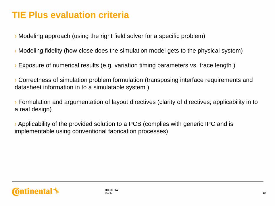
TIE Plus evaluation criteria
22
› Modeling approach (using the right field solver for a specific problem)
› Modeling fidelity (how close does the simulation model gets to the physical system)
› Exposure of numerical results (e.g. variation timing parameters vs. trace length )
› Correctness of simulation problem formulation (transposing interface requirements and
datasheet information in to a simulatable system )
› Formulation and argumentation of layout directives (clarity of directives; applicability in to
a real design)
› Applicability of the provided solution to a PCB (complies with generic IPC and is
implementable using conventional fabrication processes)
Public
IID EE HW
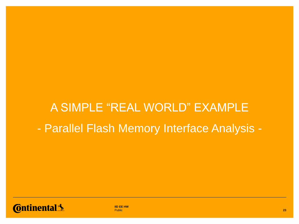
A SIMPLE “REAL WORLD” EXAMPLE
- Parallel Flash Memory Interface Analysis -
23
Public
IID EE HW
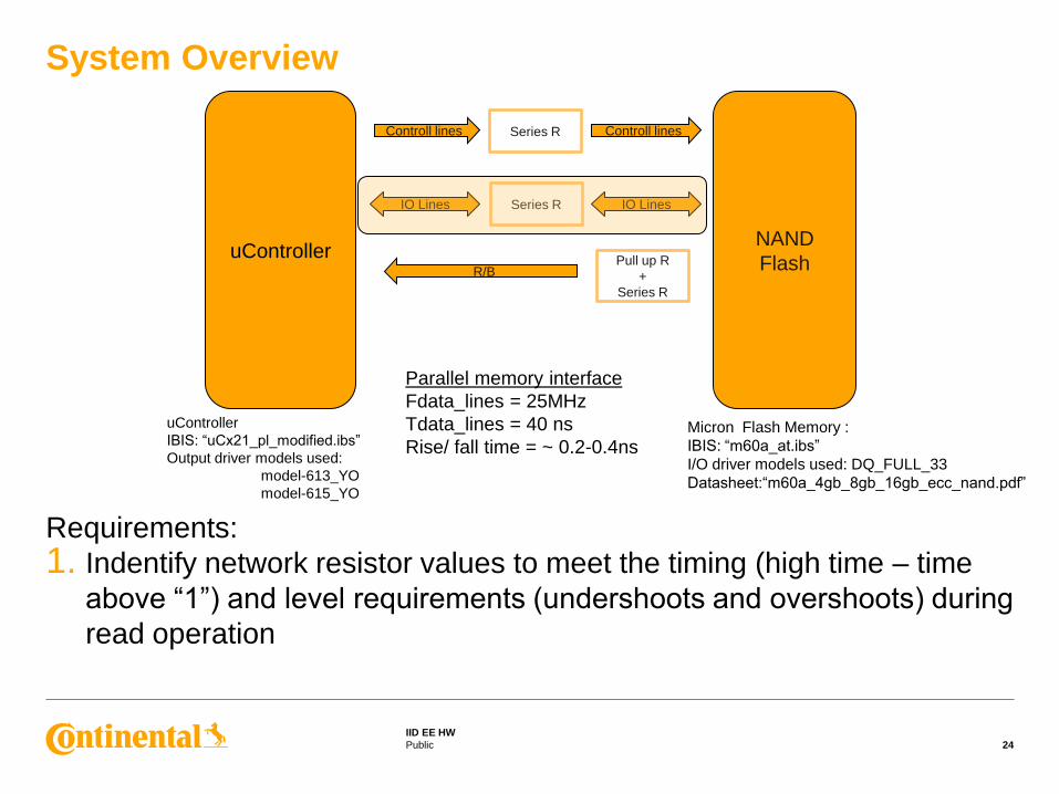
System Overview
24
uController
Controll lines
NAND
Flash R/B
IO Lines IO Lines
Pull up R
+
Series R
Controll lines Series R
Series R
uController
IBIS: “uCx21_pl_modified.ibs”
Output driver models used:
model-613_YO
model-615_YO
Micron Flash Memory :
IBIS: “m60a_at.ibs”
I/O driver models used: DQ_FULL_33
Datasheet:“m60a_4gb_8gb_16gb_ecc_nand.pdf”
Parallel memory interface
Fdata_lines = 25MHz
Tdata_lines = 40 ns
Rise/ fall time = ~ 0.2-0.4ns
Requirements:
1. Indentify network resistor values to meet the timing (high time – time
above “1”) and level requirements (undershoots and overshoots) during
read operation
Public
IID EE HW
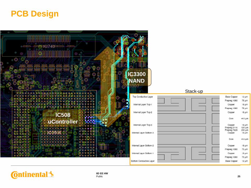
PCB Design
25
IC508
uController
IC3300
NAND
Stack-up
Public
IID EE HW
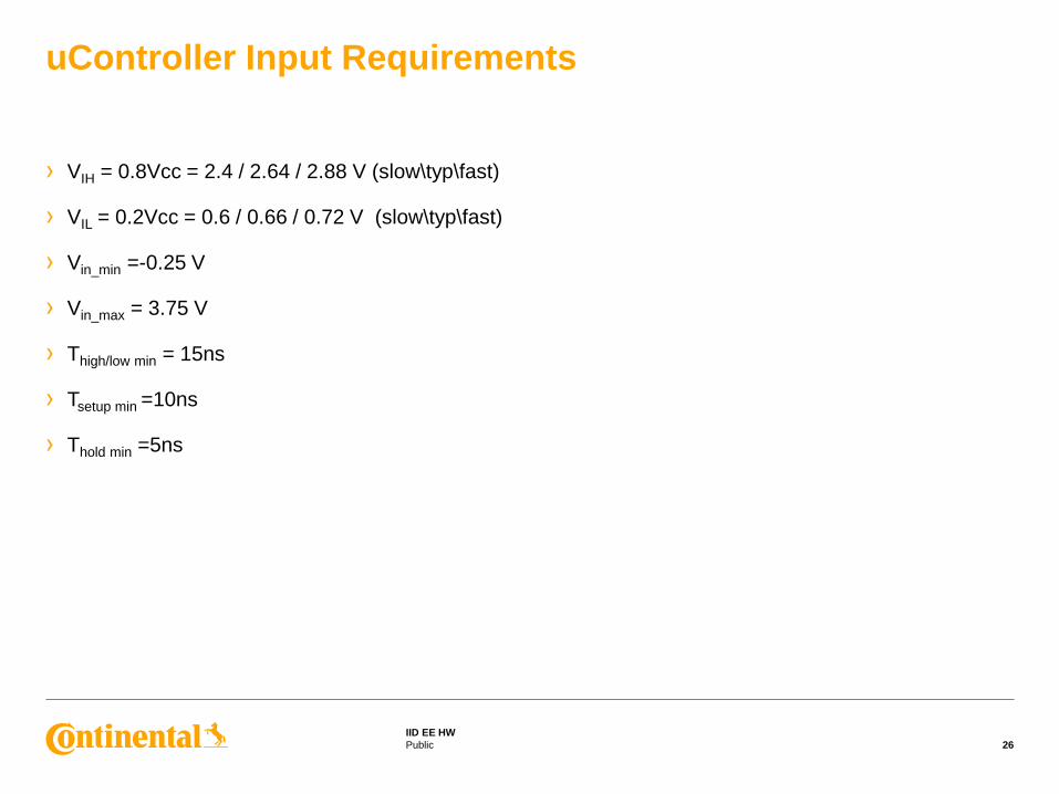
› VIH = 0.8Vcc = 2.4 / 2.64 / 2.88 V (slow\typ\fast)
› VIL = 0.2Vcc = 0.6 / 0.66 / 0.72 V (slow\typ\fast)
› Vin_min =-0.25 V
› Vin_max = 3.75 V
› Thigh/low min = 15ns
› Tsetup min =10ns
› Thold min =5ns
uController Input Requirements
26
Public
IID EE HW
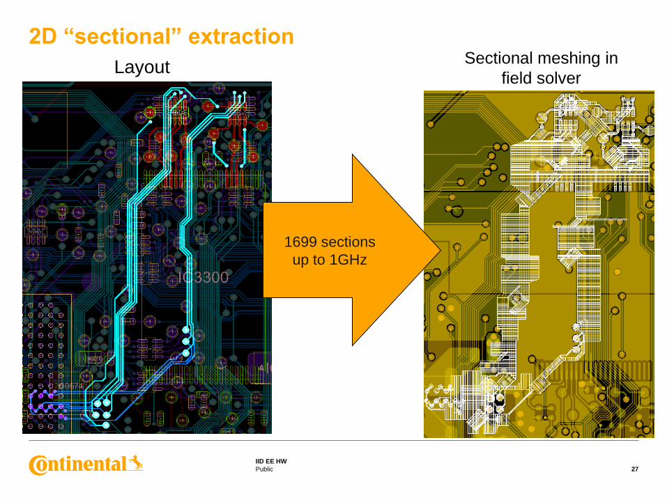
2D “sectional” extraction
27
1699 sections
up to 1GHz
Layout Sectional meshing in
field solver
Public
IID EE HW
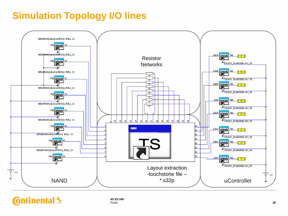
Simulation Topology I/O lines
28
uController
NAND
Resistor
Networks
Layout extraction
-touchstone file –
*.s32p
Public
IID EE HW
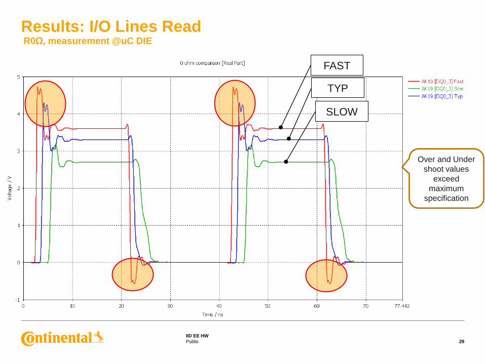
Results: I/O Lines Read R0Ω, measurement @uC DIE
29
Over and Under
shoot values
exceed
maximum
specification
FAST
TYP
SLOW
Public
IID EE HW
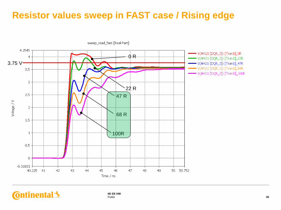
Resistor values sweep in FAST case / Rising edge
30
3.75 V
100R
68 R
47 R
22 R
0 R
Public
IID EE HW
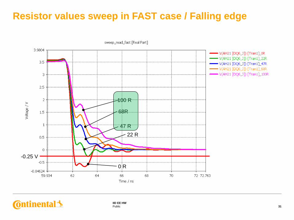
Resistor values sweep in FAST case / Falling edge
31
-0.25 V
68R
100 R
0 R
22 R
47 R
Public
IID EE HW
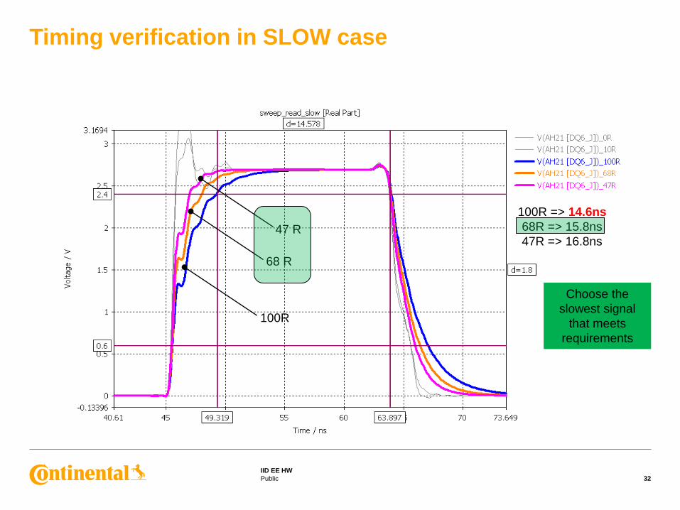
Timing verification in SLOW case
32
100R
68 R
47 R
100R => 14.6ns
68R => 15.8ns
47R => 16.8ns
Choose the
slowest signal
that meets
requirements
Public
IID EE HW
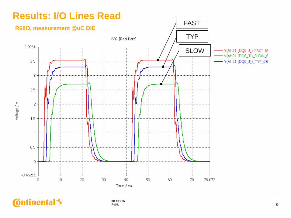
Results: I/O Lines Read R68Ω, measurement @uC DIE
33
FAST
TYP
SLOW