Embed Size (px)
Citation preview

High Speed, Video Difference Amplifier
Data Sheet AD830
Rev. D Document Feedback Information furnished by Analog Devices is believed to be accurate and reliable. However, no responsibility is assumed by Analog Devices for its use, nor for any infringements of patents or other rights of third parties that may result from its use. Specifications subject to change without notice. No license is granted by implication or otherwise under any patent or patent rights of Analog Devices. Trademarks and registered trademarks are the property of their respective owners.
One Technology Way, P.O. Box 9106, Norwood, MA 02062-9106, U.S.A.Tel: 781.329.4700 ©2005–2018 Analog Devices, Inc. All rights reserved. Technical Support www.analog.com
FEATURES Differential amplification Wide common-mode voltage range: +12.8 V to −12 V Differential voltage: ±2 V High CMRR: 60 dB at 4 MHz Built-in differential clipping level: ±2.3 V Fast dynamic performance 85 MHz unity gain bandwidth 35 ns settling time to 0.1% 360 V/μs slew rate Symmetrical dynamic response Excellent video specifications Differential gain error: 0.06% Differential phase error: 0.08° 15 MHz (0.1 dB) bandwidth Flexible operation High output drive of ±50 mA min Specified with both ±5 V and ±15 V supplies Low distortion: THD = −72 dB @ 4 MHz Excellent DC performance: 3 mV max input
Offset voltage
APPLICATIONS Differential line receiver High speed level shifter High speed in-amp Differential to single-ended conversion Resistorless summation and subtraction High speed analog-to-digital converter
CONNECTION DIAGRAM
AD8301
2
3
4
8
7
6
5C
GM
GM
X1
X2
Y1
Y2
VP
OUT
NC
VN
NC = NO CONNECT 0088
1-0
01
A = 1
Figure 1. 8-Lead Plastic PDIP (N), CERDIP (Q), and SOIC (RN) Packages
FREQUENCY (Hz)
CM
RR
(d
B)
110
3010M
50
40
1k
70
60
80
90
100
1M100k10k
VS = ±5V
VS = ±15V
0088
1-00
2
Figure 2. Common-Mode Rejection Ratio vs. Frequency
Good gain flatness and excellent differential gain of 0.06% and phase of 0.08° make the AD830 suitable for many video system applications. Furthermore, the AD830 is suited for general-purpose signal processing from dc to 10 MHz.
GENERAL DESCRIPTION The AD830 is a wideband, differencing amplifier designed for use at video frequencies but also useful in many other applications. It accurately amplifies a fully differential signal at the input and produces an output voltage referred to a user-chosen level. The undesired common-mode signal is rejected, even at high frequencies. High impedance inputs ease interfacing to finite source impedances and, thus, preserve the excellent common-mode rejection. In many respects, it offers significant improvements over discrete difference amplifier approaches, in particular in high frequency common-mode rejection.
The wide common-mode and differential voltage range of the AD830 make it particularly useful and flexible in level shifting applications but at lower power dissipation than discrete solutions. Low distortion is preserved over the many possible differential and common-mode voltages at the input and output.
9
–6
–2110k 100k 1M 10M 100M 1G
–3
0
3
6
–18
–15
–12
–9
FREQUENCY (Hz)
GA
IN (
dB
)
VS = ±5VRL = 150Ω
CL = 33pF
CL = 4.7pF
CL = 15pF
008
81-0
03
Figure 3. Closed-Loop Gain vs. Frequency, Gain = +1

AD830 Data Sheet
Rev. D | Page 2 of 20
TABLE OF CONTENTS Features .............................................................................................. 1 Applications ....................................................................................... 1 Connection Diagram ....................................................................... 1 General Description ......................................................................... 1 Revision History ............................................................................... 2 Specifications ..................................................................................... 3 Absolute Maximum Ratings ............................................................ 7
Maximum Power Dissipation ..................................................... 7 Thermal Resistance ...................................................................... 7 ESD Caution .................................................................................. 7
Typical Performance Characteristics ............................................. 8
Theory of Operation ...................................................................... 11 Traditional Differential Amplification .................................... 11 Problems With the Op Amp Based Approach ....................... 11 AD830 for Differential Amplification ..................................... 11 Advantageous Properties of the AD830 .................................. 11 Understanding the AD830 Topology ...................................... 11 Interfacing the Input .................................................................. 12 Supplies, Bypassing, and Grounding (Figure 34) ................... 14 AC-Coupled Line Receiver ....................................................... 17
Outline Dimensions ....................................................................... 19 Ordering Guide .......................................................................... 20
REVISION HISTORY 1/2018—Rev. C to Rev. D Change to Table 4 ............................................................................. 7 Changes to Ordering Guide .......................................................... 20 3/2010—Rev. B to Rev. C Updated Format .................................................................. Universal Changes to Ordering Guide .......................................................... 20 1/2003—Rev. A to Rev. B. Updated Ordering Guide ................................................................ 4 Change to Figure 30 ...................................................................... 14 Updated Outline Dimensions ..................................................... 15
Data Sheet AD830
Rev. D | Page 3 of 20
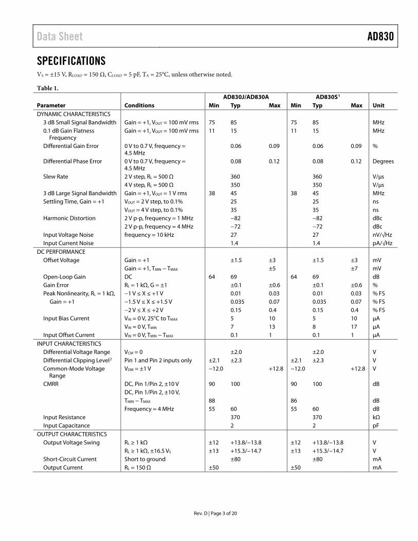
SPECIFICATIONS VS = ±15 V, RLOAD = 150 Ω, CLOAD = 5 pF, TA = 25°C, unless otherwise noted.
Table 1. AD830J/AD830A AD830S1 Parameter Conditions Min Typ Max Min Typ Max Unit DYNAMIC CHARACTERISTICS
3 dB Small Signal Bandwidth Gain = +1, VOUT = 100 mV rms 75 85 75 85 MHz 0.1 dB Gain Flatness
Frequency Gain = +1, VOUT = 100 mV rms 11 15 11 15 MHz
Differential Gain Error 0 V to 0.7 V, frequency = 4.5 MHz
0.06 0.09 0.06 0.09 %
Differential Phase Error 0 V to 0.7 V, frequency = 4.5 MHz
0.08 0.12 0.08 0.12 Degrees
Slew Rate 2 V step, RL = 500 Ω 360 360 V/μs 4 V step, RL = 500 Ω 350 350 V/μs 3 dB Large Signal Bandwidth Gain = +1, VOUT = 1 V rms 38 45 38 45 MHz Settling Time, Gain = +1 VOUT = 2 V step, to 0.1% 25 25 ns VOUT = 4 V step, to 0.1% 35 35 ns Harmonic Distortion 2 V p-p, frequency = 1 MHz −82 −82 dBc 2 V p-p, frequency = 4 MHz −72 −72 dBc Input Voltage Noise frequency = 10 kHz 27 27 nV/√Hz Input Current Noise 1.4 1.4 pA/√Hz
DC PERFORMANCE Offset Voltage Gain = +1 ±1.5 ±3 ±1.5 ±3 mV Gain = +1, TMIN − TMAX ±5 ±7 mV Open-Loop Gain DC 64 69 64 69 dB Gain Error RL = 1 kΩ, G = ±1 ±0.1 ±0.6 ±0.1 ±0.6 % Peak Nonlinearity, RL = 1 kΩ, −1 V ≤ X ≤ +1 V 0.01 0.03 0.01 0.03 % FS
Gain = +1 −1.5 V ≤ X ≤ +1.5 V 0.035 0.07 0.035 0.07 % FS −2 V ≤ X ≤ +2 V 0.15 0.4 0.15 0.4 % FS Input Bias Current VIN = 0 V, 25°C to TMAX 5 10 5 10 μA VIN = 0 V, TMIN 7 13 8 17 μA Input Offset Current VIN = 0 V, TMIN − TMAX 0.1 1 0.1 1 μA
INPUT CHARACTERISTICS Differential Voltage Range VCM = 0 ±2.0 ±2.0 V Differential Clipping Level2 Pin 1 and Pin 2 inputs only ±2.1 ±2.3 ±2.1 ±2.3 V Common-Mode Voltage
Range VDM = ±1 V −12.0 +12.8 −12.0 +12.8 V
CMRR DC, Pin 1/Pin 2, ±10 V 90 100 90 100 dB DC, Pin 1/Pin 2, ±10 V, TMIN − TMAX 88 86 dB Frequency = 4 MHz 55 60 55 60 dB Input Resistance 370 370 kΩ Input Capacitance 2 2 pF
OUTPUT CHARACTERISTICS Output Voltage Swing RL ≥ 1 kΩ ±12 +13.8/−13.8 ±12 +13.8/−13.8 V RL ≥ 1 kΩ, ±16.5 VS ±13 +15.3/−14.7 ±13 +15.3/−14.7 V Short-Circuit Current Short to ground ±80 ±80 mA Output Current RL = 150 Ω ±50 ±50 mA

AD830 Data Sheet
Rev. D | Page 4 of 20
AD830J/AD830A AD830S1 Parameter Conditions Min Typ Max Min Typ Max Unit POWER SUPPLIES
Operating Range ±4 ±16.5 ± 4 ±16.5 V Quiescent Current TMIN – TMAX 14.5 17 14.5 17 mA
+PSRR (to VP) DC, G = +1 86 86 dB −PSRR (to VN) DC, G = +1 68 68 dB
PSRR DC, G = +1, ±5 to ±15 VS 66 71 66 71 dB PSRR DC, G = +1, ±5 to ±15 VS
TMIN − TMAX 62 68 60 68 dB 1 See the Standard Military Drawing 5962-9313001MPA for specifications. 2 Clipping level function on X channel only.

Data Sheet AD830
Rev. D | Page 5 of 20
VS = ±5 V, RLOAD = 150 Ω, CLOAD = 5 pF, TA = +25°C, unless otherwise noted.
Table 2. AD830J/AD830A AD830S1
Parameter Conditions Min Typ Max Min Typ Max Units
DYNAMIC CHARACTERISTICS
3 dB Small Signal Bandwidth Gain = +1, VOUT = 100 mV rms 35 40 35 40 MHz 0.1 dB Gain Flatness Frequency Gain = +1, VOUT = 100 mV rms 5 6.5 5 6.5 MHz Differential Gain Error 0 V to 0.7 V, frequency = 4.5 MHz, Gain = +2 0.14 0.18 0.14 0.18 % Differential Phase Error 0 V to 0.7 V, frequency = 4.5 MHz, Gain = +2 0.32 0.4 0.32 0.4 Degrees Slew Rate, Gain = +1 2 V step, RL = 500 Ω 210 210 V/μs 4 V step, RL = 500 Ω 240 240 V/μs 3 dB Large Signal Bandwidth Gain = +1, VOUT = 1 V rms 30 36 30 36 MHz Settling Time VOUT = 2 V step, to 0.1% 35 35 ns VOUT = 4 V step, to 0.1% 48 48 ns Harmonic Distortion 2 V p-p, frequency = 1 MHz −69 −69 dBc 2 V p-p, frequency = 4 MHz −56 −56 dBc Input Voltage Noise Frequency = 10 kHz 27 27 nV/√Hz Input Current Noise 1.4 1.4 pA/√Hz
DC PERFORMANCE
Offset Voltage Gain = +1 ±1.5 ±3 ±1.5 ±3 mV Gain = +1, TMIN − TMAX ±4 ±5 mV Open-Loop Gain DC 60 65 60 65 dB Unity Gain Accuracy RL = 1 kΩ ±0.1 ±0.6 ±0.1 ±0.6 % Peak Nonlinearity, RL= 1 kΩ −1 V ≤ X ≤ +1 V 0.01 0.03 0.01 0.03 % FS −1.5 V ≤ X ≤ +1.5 V 0.045 0.07 0.045 0.07 % FS −2 V ≤ X ≤ +2 V 0.23 0.4 0.23 0.4 % FS Input Bias Current VIN = 0 V, 25°C to TMAX 5 10 5 10 μA VIN = 0 V, TMIN 7 13 8 17 μA Input Offset Current VIN = 0 V, TMIN − TMAX 0.1 1 0.1 1 μA
INPUT CHARACTERISTICS
Differential Voltage Range VCM = 0 ±2.0 ±2.0 V Differential Clipping Level2 Pin 1 and Pin 2 inputs only ±2.0 ±2.2 ±2.0 ±2.2 V Common-Mode Voltage Range VDM = ±1 V −2.0 +2.9 −2.0 +2.9 V CMRR DC, Pin 1/Pin 2, +4 V to −2 V 90 100 90 100 dB DC, Pin 1/Pin 2, +4 V to −2 V, TMIN − TMAX 88 86 dB Frequency = 4 MHz 55 60 55 60 dB Input Resistance 370 370 kΩ Input Capacitance 2 2 pF
OUTPUT CHARACTERISTICS Output Voltage Swing RL ≥ 150 Ω ±3.2 ±3.5 ±3.2 ±3.5 V RL ≥ 150 Ω, ±4 VS ±2.2 −2.4/+2.7 ±2.2 −2.4/+2.7 V Short-Circuit Current Short to ground −55/+70 −55/+70 mA Output Current ±40 ±40 mA

AD830 Data Sheet
Rev. D | Page 6 of 20
AD830J/AD830A AD830S1
Parameter Conditions Min Typ Max Min Typ Max Units
POWER SUPPLIES Operating Range ±4 ±16.5 ±4 ±16.5 V Quiescent Current TMIN − TMAX 13.5 16 13.5 16 mA
+PSRR (to VP) DC, G = +1, offset 86 86 dB −PSRR (to VN) DC, G = +1, Offset 68 68 dB
PSRR (Dual Supply) DC, G = +1, ±5 to ±15 VS 66 71 66 71 dB PSRR (Dual Supply) DC, G = +1, ±5 to ±15 VS
TMIN − TMAX 62 68 60 68 dB 1 See Standard Military Drawing 5962-9313001MPA for specifications. 2 Clipping level function on X channel only.

Data Sheet AD830
Rev. D | Page 7 of 20
ABSOLUTE MAXIMUM RATINGS Table 3. Parameter Rating Supply Voltage ±18 V Internal Power Dissipation Observe derating
curves Output Short-Circuit Duration Observe derating
curves Common-Mode Input Voltage ±VS Differential Input Voltage ±VS Storage Temperature Range (Q) −65°C to +150°C Storage Temperature Range (N) −65°C to +125°C Storage Temperature Range (RN) −65°C to +125°C Operating Temperature Range
AD830J 0°C to +70°C AD830A −40°C to +85°C AD830S −55°C to +125°C
Lead Temperature Range (Soldering 60 sec) 300°C
Stresses at or above those listed under Absolute Maximum Ratings may cause permanent damage to the product. This is a stress rating only; functional operation of the product at these or any other conditions above those indicated in the operational section of this specification is not implied. Operation beyond the maximum operating conditions for extended periods may affect product reliability.
MAXIMUM POWER DISSIPATION The maximum power that can be safely dissipated by the AD830 is limited by the associated rise in junction temperature. For the plastic packages, the maximum safe junction temperature is 145°C. For the CERDIP, the maximum junction temperature is 175°C. If these maximums are exceeded momentarily, proper circuit operation will be restored as soon as the die temperature is reduced. Leaving the AD830 in the overheated condition for an extended period can result in permanent damage to the device. To ensure proper operation, it is important to observe the recommended derating curves.
While the AD830 output is internally short-circuit protected, this may not be sufficient to guarantee that the maximum junction temperature is not exceeded under all conditions. If the output is shorted to a supply rail for an extended period, then the amplifier may be permanently destroyed.
THERMAL RESISTANCE θJA is specified for the worst-case conditions, that is, a device soldered in a circuit board for surface-mount packages.
Table 4. Thermal Resistance Package Type θJA Unit 28-Lead PDIP Package 90 °C/W 8-Lead SOIC Package 155 °C/W 8-Lead CERDIP Package 110 °C/W
ESD CAUTION
2.5
090
1.5
0.5
–30
1.0
–50
2.0
70503010–10
AMBIENT TEMPERATURE (°C)
TO
TA
L P
OW
ER
DIS
SIP
AT
ION
(W
)
TJ MAX = 145°C
8-LEAD PDIP
8-LEAD SOIC
008
81-0
04
2.8
0.2140
0.8
0.4
–40
0.6
–60
1.4
1.0
1.2
1.6
2.0
2.2
2.6
2.4
1.8
100 120806040200–20
AMBIENT TEMPERATURE (°C)
TO
TA
L P
OW
ER
DIS
SIP
AT
ION
(W
)
8-LEAD CERDIP
TJ MAX = 175°C
008
81-0
05
Figure 4. Maximum Power Dissipation vs. Temperature, PDIP and SOIC Packages Figure 5. Maximum Power Dissipation vs. Temperature, CERDIP Package

AD830 Data Sheet
Rev. D | Page 8 of 20
TYPICAL PERFORMANCE CHARACTERISTICS
±
FREQUENCY (Hz)
CM
RR
(d
B)
110
3010M
50
40
1k
70
60
80
90
100
1M100k10k
VS = ±15V
VS = ±5V
008
81-0
06
Figure 6. Common-Mode Rejection Ratio vs. Frequency
FREQUENCY (Hz)
–50
–70
–90M01k01 1M100k1k
–80
–60
HA
RM
ON
IC D
IST
OR
TIO
N (
dB
c)
±5V SUPPLIESSECOND HARMONIC
THIRD HARMONIC
±15V SUPPLIESSECOND HARMONIC
THIRD HARMONIC
VOUT = 2V p-pRL = 150ΩGAIN = +1
008
81-0
07
Figure 7. Harmonic Distortion vs. Frequency
JUNCTION TEMPERATURE (°C)
INP
UT
CU
RR
EN
T (
µA
)
9
3140
6
4
–40
5
–60
8
7
120806040200–20 100
0088
1-0
08
Figure 8. Input Bias Current vs. Temperature
±
±
±
FREQUENCY (Hz)
PS
RR
(d
B)
100
1010M
30
20
1k
40
50
60
70
80
90
1M100k10k
TO VP @ ±15V
TO VN @ ±15V
TO VP @ ±5V
TO VN @ ±5V
008
81-0
09
Figure 9. Power Supply Rejection Ratio vs. Frequency
±
FREQUENCY (Hz)
3
–12
–27100k 10M 100M1M10k
–9
–6
–3
0
–24
–21
–18
–15GA
IN (
dB
)
1G
±15V
±5V
±10V
RL = 150ΩCL = 4.7pF
008
81-0
10
Figure 10. Closed-Loop Gain vs. Frequency G = +1
±
±
±
JUNCTION TEMPERATURE (°C)
INP
UT
OF
FS
ET
VO
LT
AG
E (
mV
)
3
–4140
–1
–3
–40
–2
–60
2
0
1
120100806040200–20
±5VS
±10VS
±15VS
0088
1-0
11
Figure 11. Input Offset Voltage vs. Temperature

Data Sheet AD830
Rev. D | Page 9 of 20
0.10
0.03
0.01
0.02
0.06
0.04
0.05
0.07
0.08
0.09
1565
0.10
0.03
0.01
00
0.02
0.06
0.04
0.05
0.07
0.08
0.09
1413121110987SUPPLY VOLTAGE (±V)
DIF
FE
RE
NT
IAL
GA
IN (
%)
DIF
FE
RE
NT
IAL
PH
AS
E (
Deg
rees
)
PHASE
GAIN
GAIN = +2RL = 500ΩFREQ = 4.5MHz
008
81-0
12
Figure 12. Differential Gain and Phase vs. Supply Voltage, RL = 500 Ω
–40
–1002.00
–70
–90
0.50
–80
0.25
–50
–60
1.751.251.00 1.500.75
PEAK AMPLITUDE (V)
HA
RM
ON
IC D
IST
OR
TIO
N (
dB
)
HD3 ±5V100kHz
HD2 ±15V100kHz
HD2 ±5V100kHz
HD3 ±15V100kHz
0088
1-0
13
Figure 13. Harmonic Distortion vs. Peak Amplitude, Frequency = 100 kHz
50
10M01100
40
20
1k
30
100k 1M10k
FREQUENCY (Hz)
INP
UT
VO
LT
AG
E N
OIS
E (
nV
/√H
z)
008
81-0
14
Figure 14. Noise Spectral Density
0 0
0.20
15
0.06
0.02
6
0.04
5
0.12
0.08
0.10
0.14
0.16
0.18
1413121110987
SUPPLY VOLTAGE (±V)
DIF
FE
RE
NT
IAL
GA
IN (
%)
DIF
FE
RE
NT
IAL
PH
AS
E (
Deg
rees
)
0.40
0.12
0.04
0.08
0.24
0.16
0.20
0.28
0.32
0.36
PHASE
GAIN
GAIN = +2RL = 150ΩFREQ = 4.5MHz
0088
1-01
5
Figure 15. Differential Gain and Phase vs. Supply Voltage, RL = 150 Ω
–40
–1002.00
–70
–90
0.50
–80
0.25
–50
–60
1.751.251.00 1.500.75
PEAK AMPLITUDE (V)
HA
RM
ON
IC D
IST
OR
TIO
N (
dB
) HD2 ±5V4MHz
HD3 ±5V4MHz
HD2 ±15V4MHz
HD3 ±15V4MHz
008
81-0
16
Figure 16. Harmonic Distortion vs. Peak Amplitude, Frequency = 4 MHz
JUNCTION TEMPERATURE (°C)
Q
UIE
SC
EN
T S
UP
PL
Y C
UR
RE
NT
(m
A)
15.00
12.25140
13.00
12.50
–40
12.75
–60
13.75
13.25
13.50
14.00
14.25
14.50
14.75
120100806040200–20
±16.5VS
±5VS00
881-
017
Figure 17. Supply Current vs. Junction Temperature

AD830 Data Sheet
Rev. D | Page 10 of 20
3
–12
–271G1M 100M10M100k
–9
–6
–3
0
–24
–21
–18
–15
FREQUENCY (Hz)
UN
ITY
GA
IN C
ON
NE
CT
ION
GA
IN O
F 2
CO
NN
EC
TIO
N
9
–6
–21
–3
0
3
6
–18
–15
–12
–9
RL = 150ΩCL = 0pF
±15V
±5V
008
81-
018
Figure 18. Closed-Loop Gain vs. Frequency for the Three Common Connections of Figure 16
100mV
VS = ±5V
20ns
0%
100
90
10
VS = ±15V
008
81-0
19
Figure 19. Small Signal Pulse Response, RL = 150 Ω, CL = 4.7 pF, G = +1
9
–6
–211G100k 10M1M10k
–3
0
3
6
–18
–15
–12
–9
FREQUENCY (Hz)
GA
IN (
dB
)
100M
VS = ±5VRL = 150Ω
CL = 33pF
CL = 15pF
CL = 4.7pF
008
81-0
20
Figure 20. Closed-Loop Gain vs. Frequency vs. CL, G = +1, VS = ±5 V
V1 1
2
4
3
8
7
5
6
AD830
C
GM
GM
VP
VN
OUT
(a)
(b)
V1
1
2
4
3
8
7
5
6
AD830
C
A = 1
A = 1
GM
GM
VP
VN
OUT
VOUT = 2V1RESISTORLESS GAIN OF 2
VOUT = V1OP AMP CONNECTION
(c)
V1 1
2
4
3
8
7
5
6
AD830
CA = 1
GM
GM
VP
VN
OUT
VOUT = V1GAIN OF 1
008
81-0
21
Figure 21. Connection Diagrams
1V
VS = ±5V
20ns
0%
100
90
10
VS = ±15V
008
81-0
22
Figure 22. Large Signal Pulse Response, RL = 150 Ω, CL = 4.7 pF, G = +1
9
–6
–211G100k 10M1M10k
–3
0
3
6
–18
–15
–12
–9
FREQUENCY (Hz)
GA
IN (
dB
)
100M
VS = ±15VRL = 150Ω CL = 33pF
CL = 15pF
CL = 4.7pF
0088
1-0
23
Figure 23. Closed-Loop Gain vs. Frequency vs. CL, G = +1, VS = ±15 V

Data Sheet AD830
Rev. D | Page 11 of 20
THEORY OF OPERATION TRADITIONAL DIFFERENTIAL AMPLIFICATION In the past, when differential amplification was needed to reject common-mode signals superimposed with a desired signal, most often the solution used was the classic op amp based difference amplifier shown in Figure 24. The basic function VO = V1 − V2 is simply achieved, but the overall performance is poor and the circuit possesses many serious problems that make it difficult to realize a robust design with moderate to high levels of performance.
V1
VOUT
V2
R1 R2
R3
R4ONLY IF R1 = R2 = R3 = R4DOES VOUT = V1 – V2
0088
1-02
4
Figure 24. Op Amp Based Difference Amplifier
PROBLEMS WITH THE OP AMP BASED APPROACH • Low common-mode rejection ratio (CMRR) • Low impedance inputs • CMRR highly sensitive to the value of source R • Different input impedance for the + and − input • Poor high frequency CMRR • Requires very highly matched resistors, R1 to R4, to achieve
high CMRR • Halves the bandwidth of the op amp • High power dissipation in the resistors for large common-
mode voltage
AD830 FOR DIFFERENTIAL AMPLIFICATION The AD830 amplifier was specifically developed to solve the listed problems with the discrete difference amplifier approach. Its topology, discussed in detail in the Understanding the AD830 Topology section, by design acts as a difference amplifier. The circuit of Figure 25 shows how simply the AD830 is configured to produce the difference of the two signals, V1 and V2, in which the applied differential signal is exactly reproduced at the output relative to a separate output common. Any common-mode voltage present at the input is removed by the AD830.
V1
VOUT
IY
IX
V2
A = 1
V I→
V I→ VOUT = V1 – V2
0088
1-02
5
Figure 25. AD830 as a Difference Amplifier
ADVANTAGEOUS PROPERTIES OF THE AD830 • High common-mode rejection ratio (CMRR) • High impedance inputs • Symmetrical dynamic response for +1 and −1 Gain • Low sensitivity to the value of source R • Equal input impedance for the + and − input • Excellent high frequency CMRR • No halving of the bandwidth • Constant power distortion versus common-mode voltage • Highly matched resistors not needed
UNDERSTANDING THE AD830 TOPOLOGY The AD830 represents Analog Devices first amplifier product to embody a powerful alternative amplifier topology. Referred to as active feedback, the topology used in the AD830 provides inherent advantages in the handling of differential signals, differing system commons, level shifting, and low distortion, high frequency amplification. In addition, it makes possible the implementation of many functions not realizable with single op amp circuits or superior to op amp based equivalent circuits. With this in mind, it is important to understand the internal structure of the AD830.
The topology, reduced to its elemental form, is shown in Figure 26. Nonideal effects, such as nonlinearity, bias currents, and limited full scale, are omitted from this model for simplicity but are discussed later. The key feature of this topology is the use of two, identical voltage-to-current converters, GM, that make up input and feedback signal interfaces. They are labeled with inputs VX and VY, respectively. These voltage-to-current converters possess fully differential inputs, high linearity, high input impedance, and wide voltage range operation. This enables the part to handle large amplitude differential signals; it also provides high common-mode rejection, low distortion, and negligible loading on the source. The label, GM, is meant to convey that the transconductance is a large signal quantity, unlike in the front end of most op amps. The two GM stage current outputs, IX and IY, sum together at a high impedance node, which is characterized by an equivalent resistance and capacitance connected to an ac common. A unity voltage gain stage follows the high impedance node to provide buffering from loads. Relative to either input, the open-loop gain, AOL, is set by the transconductance, GM, working into the resistance, RP; AOL = GM × RP. The unity gain frequency, ω0 dB, for the open-loop gain is established by the transconductance, GM, working into the capacitance, CC; ω0 dB = GM/CC. The open-loop description of the AD830 is shown below for completeness.

AD830 Data Sheet
Rev. D | Page 12 of 20
VX1
VOUT
IY
IX
CC
A = 1
GM
AOLS=GMRP
VX2
GMVY1
VY2RP
IZ
IX = (VX1 – VX2) GMIY = (VY1 – VY2) GMIZ = IX + IY
1 + S (CCRP)
0088
1-02
6
Figure 26. Topology Diagram
VX1
VOUT
IY
IX
CC
A = 1
GM
1
VX2
GMVY1
VY2
VX1 – VX2 = VY2 – VY1FOR VY2 = VOUTVOUT = (VX1 – VX2 + VY1)
1 + S(CC/GM) 0088
1-02
7
Figure 27. Closed-Loop Connection
Precise amplification is accomplished through closed-loop operation of this topology. Voltage feedback is implemented via the Y GM stage where the output is connected to the −Y input for negative feedback, as shown in Figure 27. An input signal is applied across the X GM stage, either fully differential or single-ended referred to common. It produces a current signal that is summed at the high impedance node with the output current from the Y GM stage. Negative feedback nulls this sum to a small error current necessary to develop the output voltage at the high impedance node. The error current is usually negligible, so the null condition essentially forces the Y GM output stage current to equal the exact X GM output current. Because the two transconductances are identical, the differential voltage across the Y inputs equals the negative of the differential voltage across the X input; VY = −VX or, more precisely, VY2 − VY1 = VX1 − VX2. This simple relation provides the basis to easily analyze any function possible to synthesize with the AD830, including any feedback situation.
The bandwidth of the circuit is defined by the GM and the capacitor, CC. The highly linear GM stages give the amplifier a single-pole response, excluding the output amplifier and loading effects. It is important to note that the bandwidth and general dynamic behavior is symmetrical (identical) for the noninverting and the inverting connections of the AD830. In addition, the input impedance and CMRR are the same for either connection. This is very advantageous and unlike in a voltage or current feedback amplifier where there is a distinct difference in performance between the inverting and noninverting gain. The practical importance of this cannot be overemphasized and is a key feature offered by the AD830 amplifier topology.
INTERFACING THE INPUT Common-Mode Voltage Range
The common-mode range of the AD830 is defined by the amplitude of the differential input signal and the supply voltage. The general definition of common-mode voltage, VCM, is usually applied to a symmetrical differential signal centered around a particular voltage, as illustrated in Figure 28. This is the meaning implied here for common-mode voltage. The internal circuitry establishes the maximum allowable voltage on the input or feedback pins for a given supply voltage. This constraint and the differential input voltage sets the common-mode voltage limit. Figure 29 shows a curve of the common-mode voltage range versus the differential voltage for three supply voltage settings.
VMAX
VCMVPEAK
0088
1-02
8
Figure 28. Common-Mode Definition
DIFFERENTIAL INPUTVOLTAGE (VPEAK)
15
00 2.0
CO
MM
ON
-MO
DE
VOLT
AGE
(±V)
0.4 0.8 1.2 1.6
6
3
12
9
±5V = VS
±15V = VS
–VCM
–VCM
+VCM
+VCM
+VCM
±10V = VS
–VCM
0088
1-02
9
Figure 29. Input Common-Mode Voltage Range vs. Differential Input Voltage
Differential Voltage Range
The maximum applied differential voltage is limited by the clipping range of the input stages. This is nominally set at a 2.4 V magnitude and depicted in the cross plot (X-Y) in Figure 30. The useful linear range of the input stages is set at 2 V but is actually a function of the distortion required for a particular application. The distortion increases for larger differential input voltages. A plot of relative distortion versus the input differential voltage is shown in Figure 13 and Figure 16. The distortion characteristics impose a secondary limit to the differential input voltage for high accuracy applications.

Data Sheet AD830
Rev. D | Page 13 of 20
10
0%
10090
1V 1V
0088
1-03
0
Figure 30. Clipping Behavior
Choice of Polarity
The sign of the gain is easily selected by choosing the polarity of the connections to the + and − inputs of the X GM stage. Swapping between inverting and noninverting gain is possible simply by reversing the input connections. The response of the amplifier is identical in either connection, except for the sign change.
The bandwidth, high impedance, and transient behavior of the AD830 is symmetrical for both polarities of gain. This is very advantageous and unlike an op amp.
Input Impedance
The relatively high input impedance of the AD830, for a differential receiver amplifier, permits connections to modest impedance sources without much loading or loss of common-mode rejection. The nominal input resistance is 300 kΩ. The real limit to the upper value of the source resistance is in its effect on common-mode rejection and bandwidth. If the source resistance is in only one input, then the low frequency common-mode rejection is lowered to ≈ RIN/RS. The source resistance/input capacitance pole limits the bandwidth. Refer to the following equation:
××
π= INS CRf
21
Furthermore, the high frequency common-mode rejection is additionally lowered by the difference in the frequency response caused by the RS × CIN pole. Therefore, to maintain good low and high frequency common-mode rejection, it is recommended that the source resistances of the + and − inputs be matched and of modest value (≤10 kΩ).
Handling Bias Currents
The bias currents are typically 4 μA flowing into each pin of the GM stages of the AD830. Because all applications possess some finite source resistance, the bias current through this resistor creates a voltage drop (IBIAS × RS). The relatively high input impedance of the AD830 permits modest values of RS, typically ≤10 kΩ. If the source resistance is in only one terminal, then an objectionable offset voltage may result, for example, 4 μA × 5 kΩ = 20 mV. Placement of an equal value resistor in series with the other input cancels the offset to first order. However, due to
mismatches in the resistances, a residual offset remains and is likely to be greater than the bias current (offset current) mismatches.
Applying Feedback
The AD830 is intended for use with gains from 1 to 100. Gains greater than one are simply set by a pair of resistors connected as shown in the difference amplifier (Figure 40) with gain >1. The value of the bottom resistor, R2, should be kept less than 1 kΩ to ensure that the pole formed by CIN and the parallel connection of R1 and R2 is sufficiently high in frequency so that it does not introduce excessive phase shift around the loop and destabilize the amplifier. A compensating resistor, equal to the parallel combination of R1 and R2, should be placed in series with the other Y GM stage input to preserve the high frequency common-mode rejection and to lower the offset voltage induced by the input bias current.
Output Common Mode
The output swing of the AD830 is defined by the differential input voltage, the gain, and the output common. Depending on the anticipated signal span, the output common (or ground) may be set anywhere between the allowable peak output voltage in a manner similar to that described for input voltage common mode. A plot of the peak output voltage versus the supply is shown in Figure 31. A prediction of the common-mode range versus the peak output differential voltage can be easily derived from the maximum output swing as VOCM = VMAX − VPEAK.
SUPPLY VOLTAGE (V)
15
0200
MA
XIM
UM
OU
TPU
T SW
ING
(±V)
4 8 12 16
6
3
12
9VN
VP
0088
1-03
1
Figure 31. Maximum Output Swing vs. Supply
Output Current
The absolute peak output current is set by the short-circuit current limiting, typically greater than 60 mA. The maximum drive capability is rated at 50 mA but without a guarantee of distortion performance. Best distortion performance is obtained by keeping the output current ≤20 mA. Attempting to drive large voltages into low valued resistances, for example, 10 V into 150 Ω causes an apparent lowering of the limit for output signal swing but is just the current limiting behavior.

AD830 Data Sheet
Rev. D | Page 14 of 20
Driving Cap Loads
The AD830 is capable of driving modest sized capacitive loads while maintaining its rated performance. Several curves of bandwidth versus capacitive load are given in Figure 34 and Figure 37. The AD830 was designed primarily as a low distortion video speed amplifier but with a trade-off, for example, giving up very large capacitive load driving capability. If very large capacitive loads must be driven, the network shown in Figure 32 should be used to ensure stable operation. If the loss of gain caused by the resistor, RS, in series with the load is objectionable, the optional feedback network shown may be added to restore the lost gain.
+VS
VOUTRS
36.5Ω
*OPTIONAL FEEDBACK NETWORK
–VS
AD8301
2
3
4
8
7
6
5
A = 1
GM
GM C
0.1µF
0.1µF
C1100pF
RS
R2
R11kΩ
INPUTSIGNAL
VCM
ZCM
00
88
1-0
32
Figure 32. Circuit for Driving Large Capacitive Loads
FREQUENCY (Hz)
3
10k
CL
OS
ED
-LO
OP
AM
PL
ITU
DE
RE
SP
ON
SE
(d
B)
–27100k 1M 10M 100M
±15V
±5V
–24
–21
–18
–15
–12
–9
–6
–3
0
008
81-0
33
Figure 33. Closed-Loop Response vs. Frequency with 100 pF Load and Series
Resistor Compensation
SUPPLIES, BYPASSING, AND GROUNDING (FIGURE 34) The AD830 is capable of operating over a wide range of supply voltages, both single and dual supplies. The coupling may be dc or ac, provided the input and output voltages stay within the specified common-mode voltage limits. For dual supplies, the device works from ±4 V to ±16.5 V. Single-supply operation is possible over 8 V to 33 V. It is also possible to operate the part with split-supply voltages, for example, +24 V or −5 V for special applications such as level shifting. The primary constraint is that the total potential between the two supplies does not exceed 33 V.
Inclusion of power supply bypassing capacitors is necessary to achieve stable behavior and the specified performance. It is especially important when driving low resistance loads. At minimum, connect a 0.1 μF ceramic capacitor at the supply lead of the AD830 package. In addition, for the best bypassing, it is best to connect a 0.01 μF ceramic capacitor and 4.7 μF tantalum capacitor to the supply lead going to the AD830.
0.1µF 0.01µF
VPAND
VN
VPAND
VN4.7µF
LOADGNDLEAD
LOADGNDLEAD
008
81-0
34
Figure 34. Supply Decoupling Options
The AD830 is designed to be capable of rejecting noise and dissimilar potentials in the ground lines. Therefore, proper care is necessary to realize the benefits of the differential amplification of the part. Separation of the input and output grounds is crucial in rejection of the common-mode noise at the inputs and eliminating any ground drops on the input signal line. For example, connecting the ground of a coaxial cable to the AD830 output common (board ground) could degrade the CMR and also introduce power-down loading on cable grounds.
However, it is also necessary as in any electronic system to provide a return path for bias currents back to their original power supply. This is accomplished by providing a connection between the differing grounds through a modest impedance labeled ZCM, for example, 100 Ω.
Single-Supply Operation
The AD830 is capable of operating in single power supply applications down to a voltage of 8 V, with the generalized connection shown in Figure 35. There is a constraint on the common-mode voltage at the input and output that establishes the range for these voltages. Direct coupling may be used for input and output voltages that lie in these ranges. Any gain network applied needs to be referred to the output common connection or have an appropriate offset voltage. In situations where the signal lies at a common voltage outside the common-mode range of the AD830, direct coupling does not work, so ac coupling should be used. Figure 47 shows how to easily accomplish coupling to the AD830. For single-supply operation where direct coupling is desired, the input and output common-mode curves (Figure 36 and Figure 37) should be used.

Data Sheet AD830
Rev. D | Page 15 of 20
VP
VOUT
AD8301
2
3
4
8
7
6
5
A = 1
C
VICM
VIN
VOCMVOUT = (VIN – VICM) + VOCM
GM
GM
0088
1-03
5
Figure 35. General Single-Supply Connection
DIFFERENTIAL INPUTVOLTAGE (VPEAK)
16
00 2.0
CO
MM
ON
-MO
DE
VOLT
AG
E LI
MIT
S (±
V)
0.4 1.2 1.60.8
8
4
12
VP = +30V
VP = +15V
VP = +10V
TO GND
20
24
2830
0088
1-03
6
Figure 36. Input Common-Mode Range for Single Supply
SUPPLY VOLTAGE (V)
16
03010
MA
XIM
UM
OU
TPU
T SW
ING
(±V)
14 18 22 26
8
4
12
20
24
28
TO VP
TO GND
0088
1-03
7
Figure 37. Output Swing Limit for Single Supply
Differential Line Receiver
The AD830 is specifically designed to perform as a differential line receiver. The circuit in Figure 38 shows how simple it is to configure the AD830 for this function. The signal from System A is received differentially relative to the common of System A, and that voltage is exactly reproduced relative to the common in System B. The common-mode rejection versus frequency, shown in Figure 6, is excellent, typically 100 dB at low frequencies. The high input impedance permits the AD830 to operate as a bridging amplifier across low impedance terminations with negligible loading. The differential gain and phase specifications
are very good, as shown in Figure 12 for 500 Ω and Figure 15 for 150 Ω. The input and output common should be separated to achieve the full CMR performance of the AD830 as a differential amplifier. However, a common return path is necessary between System A and System B.
COMMON INSYSTEM A
VN
AD8301
2
3
4
8
7
6
5
A = 1
GM
GM C
VCM
ZCM
COMMON INSYSTEM B
VP
VOUT
0.1µF
0.1µF
INPUTSIGNAL
V1
V2
VOUT = V1 – V2
0088
1-03
8
Figure 38. Differential Line Receiver
Wide Range Level Shifter
The wide common-mode range and accuracy of the AD830 allows easy level shifting of differential signals referred to an input common-mode voltage to any new voltage defined at the output. The inputs may be referenced to levels as high as 10 V at the inputs with a ±2 V swing around 10 V. In the circuit in Figure 39, the output voltage, VOUT, is defined by the simple equation shown below. The excellent linearity and low distortion are preserved over the full input and output common-mode range. The voltage sources need not be of low impedance, since the high input resistance and modest input bias current of the AD830 V-to-I converters permit the use of resistive voltage dividers as reference voltages.
GM
VP
VOUT
INPUTCOMMON
VN
0.1µF
AD8301
2
3
4
8
7
6
5
A = 1
C
0.1µF
INPUTSIGNAL
V1
V2
OUTPUTCOMMON
V3VOUT = V1 – V2 + V3
0088
1-03
9
GM
Figure 39. Differential Amplification with Level Shifting
Difference Amplifier with Gain > 1
The AD830 can provide instrumentation amplifier style and differential amplification at gains greater than 1. The input signal is connected differentially and the gain is set via feedback resistors, as shown in Figure 40. The gain is G = (R2 + R1)/R2. The AD830 can provide either inverting or noninverting differential amplification. The polarity of the gain is established by the polarity of the connection at the input. Feedback resistor, R2, should generally be R2 ≤ 1 kΩ to maintain closed-loop

AD830 Data Sheet
Rev. D | Page 16 of 20
stability and also keep bias current induced offsets low. Highest CMRR and lowest dc offsets are preserved by including a compensating resistor in series with Pin 3. The gain may be as high as 100.
0.1µF
0.1µF
VP
VOUT
VN
AD8301
2
3
4
8
7
6
5
A = 1
CGM
GMINPUT
SIGNALVCM
ZCM
V1
V2
R1 R2
R2
R1
VOUT = (V1 – V2)(1 + R1/R2)00
881-
040
Figure 40. Gain of G Differential Amplifier, G>1
Offsetting the Output With Gain
Some applications, such as ADCs, require that the signal be amplified and also offset, typically to accommodate the input range of the device. The AD830 can offset the output signal very simply through Pin 3 even with gain > 1. The voltage applied to Pin 3 must be attenuated by an appropriate factor so that V3 × G = desired offset. In Figure 41, a resistive divider from a voltage reference is used to produce the attenuated offset voltage.
VP
VOUT
VN
AD8301
2
3
4
8
7
6
5
A = 1
GM
GM C
0.1µF
0.1µF
INPUTSIGNAL
VCM
ZCM
V1
V2
R1 R2
R2
R1
R3
R4
V3
VREF
VOUT = (V1 – V2)(1 + R1/R2)
0088
1-04
1
Figure 41. Offsetting the Output with Differential Gain >1
Loop Through or Line Bridging Amplifier (Figure 42)
The AD830 is ideally suited for use as a video line bridging amplifier. The video signal is tapped from the conductor of the cable relative to its shield. The high input impedance of the AD830 provides negligible loading on the cable. More significantly, the benign loading is maintained while the AD830 is powered down. Coupled with its good video load driving performance, the AD830 is well suited for video cable monitoring applications.
VP
VOUT
VN
AD8301
2
3
4
8
7
6
5
A = 1
GM
CGM
RG
249Ω
OPTIONAL CC
499Ω
499Ω
75Ω
75Ω
0.1µF
0.1µF
0088
1-04
2
Figure 42. Cable Tap Amplifier
Resistorless Summing
Direct, two input, resistorless summing is easily realized from the general unity gain mode. By grounding VX2 and applying the two inputs to VX1 and VY1, the output is the exact sum of the applied voltages, V1 and V3, relative to common; VOUT = V1 + V3. A diagram of this simple but potent application is shown below in Figure 43. The AD830 summing circuit possesses several virtues not present in the classic op amp based summing circuits.
It has high impedance inputs, no resistors, very precise summing, high reverse isolation, and noninverting gain. Achieving this function and performance with op amps requires significantly more components.
VP
OUT
VN
AD8301
2
3
4
8
7
6
5
A = 1
GM
CGM
V1
V3
VOUT = V1 +V3 0088
1-04
3
Figure 43. Resistorless Summing Amplifier
2× Gain Bandwidth Line Driver
A gain of two, without the use of resistors, is possible with the AD830. This is accomplished by grounding VX2, tying the VX1 and VY1 inputs together, and applying the input, VIN, to this wired connection. The output is exactly twice the applied voltage, VIN; VOUT = 2 × VIN. Figure 44 shows the connections for this highly useful application. The most notable characteristic of this alternative gain of +2 is that there is no loss of bandwidth as in a voltage feedback op amp based gain of +2 where the bandwidth is halved; therefore, the gain bandwidth is doubled. In addition, this circuit is accurate without the need for any precise valued resistors, as in the op amp equivalents, and it possesses excellent differential gain and phase performance, as shown in Figure 45 and Figure 46.

Data Sheet AD830
Rev. D | Page 17 of 20
75Ω
75Ω
VP
VOUT
VN
AD8301
2
3
4
8
7
6
5
A = 1
GM
GM C
0.1µF
0.1µF
VIN
008
81-0
44
Figure 44. Full Bandwidth Line Driver (G = +2)
SUPPLY VOLTAGE (±V)
0.05
0.01
515
DIF
FE
RE
NT
IAL
GA
IN (
%)
1217 3 14
0.04
0.06
0.07
0.09
GAIN
PHASE
GAIN = +2RL = 150ΩFREQ = 3.58MHz0 TO 0.7V
1110986
0.02
0.03
0.10
0.08
DIF
FE
RE
NT
IAL
PH
AS
E (
Deg
rees
)
0.16
0.04
0.06
0.14
0.18
0.02
0.12
0.10
0.08
0.20
008
81-0
45
Figure 45. Differential Gain and Phase for the Circuit of Figure 44
FREQUENCY (Hz)
0.2
10k
AM
PL
ITU
DE
RE
SP
ON
SE
(d
B)
–0.8100k 1M 10M 100M
–0.7
–0.6
–0.5
–0.4
–0.3
–0.2
–0.1
0
0.1VS = ±15V
RL = 150Ω
GAIN = +2VS = ±10V
VS = ±5V
008
81-
046
Figure 46. 0.1 dB Gain Flatness for the Circuit of Figure 44
AC-COUPLED LINE RECEIVER The AD830 is configurable as an ac-coupled differential amplifier on a single- or bipolar-supply voltage. All that is needed is inclusion of a few noncritical passive components, as illustrated in Figure 47. A simple resistive network at the X GM input establishes a common-mode bias. Here, the common mode is centered at 6 V, but in principle can be any voltage within the common-mode limits of the AD830. The 10 kΩ resistors to each input bias the X GM stage with sufficiently high impedance to keep the input coupling corner frequency low, but not too large so that residual bias current induced offset voltage becomes troublesome. For dual-supply operation, the 10 kΩ resistors may go directly to ground. The output common is conveniently set by a Zener diode for a low impedance reference to preserve the high frequency CMR. However, a simple resistive divider works fine, and good high frequency CMR can be maintained by placing a compensating resistor in series with the +Y input. The excellent CMRR response of the circuit is shown in Figure 48. A plot of the 0.1 dB flatness from 10 Hz is also shown. With the use of 10 μF capacitors, the CMR is >90 dB down to a few tens of hertz. This level of performance is almost impossible to achieve with discrete solutions.
75Ω
75Ω
+12V
VOUT
1000µF
10µF
10µF
AD8301
2
3
4
8
7
6
5
A = 1
GM
GM C
0.1µF
ZCM
75ΩCOAX
CABLE
+12V
4.7kΩ
6.8V1N4736
INPUTSIGNAL
RT
10kΩ10kΩ
2kΩ*+VS
10kΩ
10kΩ
*OPTIONAL TUNING FOR IMPROVING VERY LOW FREQUENCY CMR.
0088
1-0
47
Figure 47. AC-Coupled Line Receiver

AD830 Data Sheet
Rev. D | Page 18 of 20
FREQUENCY (Hz)
20
CO
MM
ON
-MO
DE
RE
JEC
TIO
N (
dB
)
40
60
80
100
120
WITH CIRCUIT TRIMMED USINGEXTERNAL 2kΩ POTENTIOMETER
WITHOUT EXTERNAL2kΩ POTENTIOMETER
10 100 1k 10k 100k 1M 10M 100M
0088
1-0
48
FREQUENCY (Hz)
–0.910
AM
PL
ITU
DE
RE
SP
ON
SE
(d
B)
100 1k 10k 100k 1M 10M
–0.8
–0.7
–0.6
–0.5
–0.4
–0.3
–0.2
–0.1
0
0.1
008
81-0
49
Figure 48. Common-Mode Rejection vs. Frequency for Line Receiver Figure 49. Amplitude Response vs. Frequency for Line Receiver

Data Sheet AD830
Rev. D | Page 19 of 20
OUTLINE DIMENSIONS
COMPLIANT TO JEDEC STANDARDS MS-001CONTROLLING DIMENSIONS ARE IN INCHES; MILLIMETER DIMENSIONS(IN PARENTHESES) ARE ROUNDED-OFF INCH EQUIVALENTS FORREFERENCE ONLY AND ARE NOT APPROPRIATE FOR USE IN DESIGN.CORNER LEADS MAY BE CONFIGURED AS WHOLE OR HALF LEADS. 07
0606
-A
0.022 (0.56)0.018 (0.46)0.014 (0.36)
SEATINGPLANE
0.015(0.38)MIN
0.210 (5.33)MAX
0.150 (3.81)0.130 (3.30)0.115 (2.92)
0.070 (1.78)0.060 (1.52)0.045 (1.14)
8
1 4
5 0.280 (7.11)0.250 (6.35)0.240 (6.10)
0.100 (2.54)BSC
0.400 (10.16)0.365 (9.27)0.355 (9.02)
0.060 (1.52)MAX
0.430 (10.92)MAX
0.014 (0.36)0.010 (0.25)0.008 (0.20)
0.325 (8.26)0.310 (7.87)0.300 (7.62)
0.195 (4.95)0.130 (3.30)0.115 (2.92)
0.015 (0.38)GAUGEPLANE
0.005 (0.13)MIN
Figure 50. 8-Lead Plastic Dual-in-Line Package [PDIP]
(N-8) Dimensions shown in inches and (millimeters)
CONTROLLING DIMENSIONS ARE IN MILLIMETERS; INCH DIMENSIONS(IN PARENTHESES) ARE ROUNDED-OFF MILLIMETER EQUIVALENTS FORREFERENCE ONLY AND ARE NOT APPROPRIATE FOR USE IN DESIGN.
COMPLIANT TO JEDEC STANDARDS MS-012-AA
0124
07-A
0.25 (0.0098)0.17 (0.0067)
1.27 (0.0500)0.40 (0.0157)
0.50 (0.0196)0.25 (0.0099) 45°
8°0°
1.75 (0.0688)1.35 (0.0532)
SEATINGPLANE
0.25 (0.0098)0.10 (0.0040)
41
8 5
5.00 (0.1968)4.80 (0.1890)
4.00 (0.1574)3.80 (0.1497)
1.27 (0.0500)BSC
6.20 (0.2441)5.80 (0.2284)
0.51 (0.0201)0.31 (0.0122)
COPLANARITY0.10
Figure 51. 8-Lead Standard Small Outline Package [SOIC_N]
(R-8) Dimensions shown in millimeters and (inches)

AD830 Data Sheet
Rev. D | Page 20 of 20
CONTROLLING DIMENSIONS ARE IN INCHES; MILLIMETER DIMENSIONS(IN PARENTHESES) ARE ROUNDED-OFF INCH EQUIVALENTS FORREFERENCE ONLY AND ARE NOT APPROPRIATE FOR USE IN DESIGN.
0.310 (7.87)0.220 (5.59)
0.005 (0.13)MIN
0.055 (1.40)MAX
0.100 (2.54) BSC
15° 0°
0.320 (8.13)0.290 (7.37)
0.015 (0.38)0.008 (0.20)SEATING
PLANE
0.200 (5.08)MAX
0.405 (10.29) MAX
0.150 (3.81)MIN
0.200 (5.08)0.125 (3.18)0.023 (0.58)0.014 (0.36) 0.070 (1.78)
0.030 (0.76)
0.060 (1.52)0.015 (0.38)
1 4
58
Figure 52. 8-Lead Ceramic Dual In-Line Package [CERDIP] (Q-8)
Dimensions shown in inches and (millimeters)
ORDERING GUIDE Model1, 2 Temperature Range Package Description Package Option
AD830ANZ −40°C to +85°C 8-Lead PDIP N-8 AD830ARZ −40°C to +85°C 8-Lead SOIC_N R-8 AD830ARZ-REEL7 −40°C to +85°C 8-Lead SOIC_N R-8 AD830JRZ 0°C to +70°C 8-Lead SOIC_N R-8 AD830JRZ-R7 0°C to +70°C 8-Lead SOIC_N R-8 5962-9313001MPA −55°C to +125°C 8-Lead CERDIP Q-8
1 Z = RoHS Compliant Part. 2 See Standard Military Drawing 5962-9313001 MPA for specifications.
©2005–2018 Analog Devices, Inc. All rights reserved. Trademarks and registered trademarks are the property of their respective owners.
D00881-0-1/18(D)