Embed Size (px)
Citation preview

High Speed WDS Spectrometer for SEM Provides Rapid Identification of Overlapped Peaks from Minor and Trace Constituents
John Konopka, Bill Sgammato Thermo Fisher Scientific, Madison WI

2 High Speed WDS Spectrometer for SEM Provides Rapid Identi� cation of Overlapped Peaks from Minor and Trace Constituents
High Speed WDS Spectrometer for SEM Provides Rapid Identification of Overlapped Peaks from Minor and Trace ConstituentsJohn Konopka, Bill SgammatoThermo Fisher Scientific, Madison WI
ConclusionsA new design of a WDS spectrometer has been successfully engineered which brings the high resolving power of a wavelength dispersive spectroscopy to the regime of SEM/EDS. Non-experts using non-specialized electron microscopes now have access to this tool to complement their energy dispersive spectrometers.
References1. Woldseth, R. (1973) Everything You Wanted to Know About Xray Energy Dispersive
Spectrometry. p3.10, Burlingame: Kevex
2. Heinrich, K. F. J. (1981) Electron Beam X-ray Microanalysis. p104, New York: Van Nostrand.
OverviewA wavelength dispersive x-ray spectrometer (WDS) has been developed as a complement to an energy dispersive X-ray spectrometer (EDS).
The device was engineered to be extremely fast, easily used by a broad class of analysts and easily adapted to a wide range of scanning electron microscopes (SEM).
The result is a device that is almost as easy to use as EDS yet provides far higher spectral resolution, giving the analyst an improved tool for quickly identifying overlapped x-ray lines and locating x-ray lines arising from trace elements.
IntroductionEDS is an extremely versatile technique for x-ray spectroscopy in the SEM. It is largely insensitive to changes in sample height (i.e., working distance or topography) as well as being able to a observe a wide area of the sample.(1)
EDS detectors capture the entire spectrum in one acquisition. This has the advantage that the measurements for all elements are acquired under identical conditions.
Newer silicon drift detectors (SDD) are roughly an order of magnitude larger than detectors were at their inception. This is important as characteristic x-rays produced in the SEM are relatively rare. Many electrons strike the sample without producing acharacteristic x-ray, and many x-rays that are produced are not detected.
Finally, EDS is very easy to use, requiring almost no set-up before acquiring data. The one drawback is that the spectral resolution is less than optimum. The native width of an x-ray emission line is of the order of 1 electron volt (eV), while typical SDD resolution is of the order of 100 eV depending on the energy being measured.
To meet this need for better resolution a new kind of WDS instrument has been developed as a complement to the EDS spectrometer.
MethodsTraditional WDS instruments, whether dedicated electron microprobe (EMPA) instruments or those designed for use on smaller electron columns, have been employed for precision analysis and quantitative analysis. The primarily goal of the new WDS instrument is to provide high energy resolution to the EDS analyst as a qualitative tool.
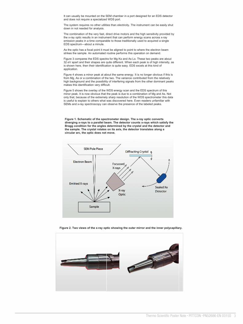
The geometry of the instrument is shown in Figure 1. Traditional WDS instruments typically use a focusing geometry such as the Johansson spectrometer(2). This design produces a large design as both the diffracting crystal and the x-ray detector must move along a focusing circle depending on the energy being observed.
In the geometry of the newer WDS instrument there is no focusing circle. Rather, a focusing optic is used to convert the diverging x-rays from the sample to a parallel beam. The parallel beam is diffracted from a flat resolving crystal and measured by a detector. The detector rotates and moves in an arc to determine the Bragg angle for the wavelength of x-ray being measured.
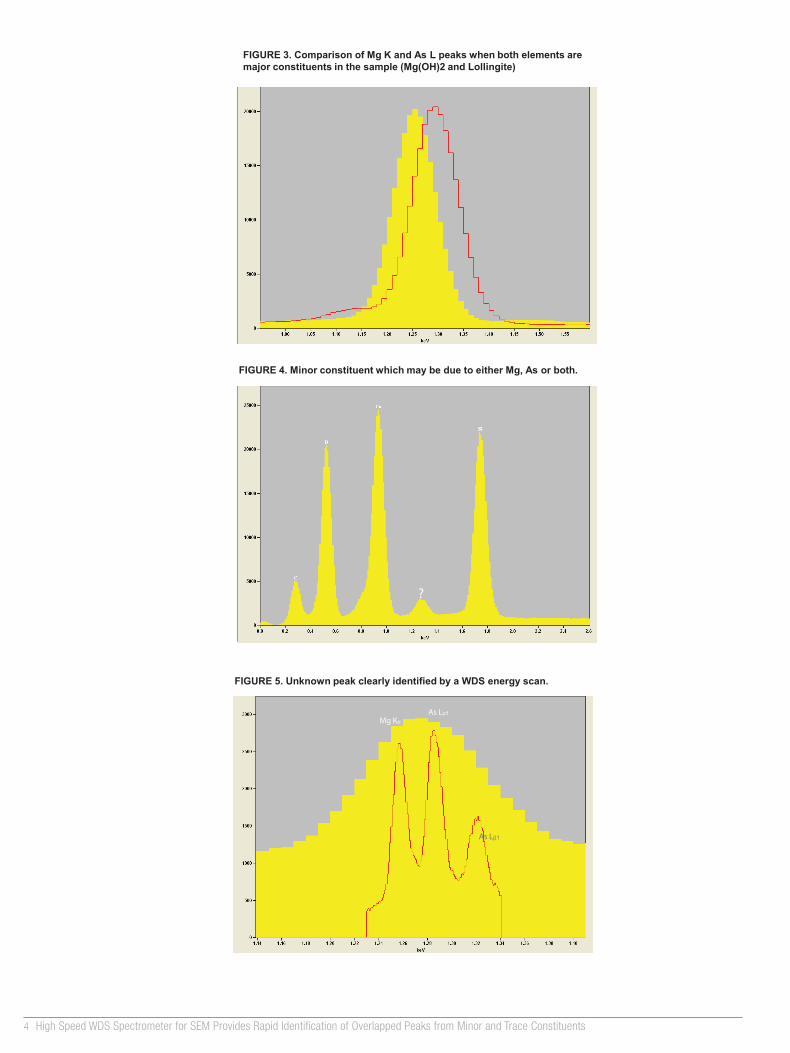
Here the x-ray optic is a compound device comprised of a grazing incident parabolic cylindrical mirror and a polycapillary inside of that. The mirror is more effective focusing low energy x-rays below about 1.7 keV and the polycarpellary is more effective at focusing x-rays above 1.7 keV. The combined device provides full coverage of the x-ray spectrum from about 100 eV to over 10 keV.
A photograph of the optic is shown in Figure 2. The optic is maintained at the end of a tube near the sample.
The detector is a sealed, xenon-filled proportional device that requires no maintenance. Traditional WDS detectors used a flow proportional detector that requires a continuous supply of P10 gas.
Because of the simpler geometry only rotational motions are required. In this design one motor rotates the resolving crystal and one motor rotates the detector arm. These are direct drive motors with no belts, gears or pulleys.
Traditional WDS spectrometer systems require the operator to select some x-ray energy dependent values for the detector bias voltage and the single channel analyzer (SCA). In this system these parameters are managed by algorithms so that no user input is required to operate the system beyond selecting the energy range to measure.
ResultsThe resulting instrument meets the goals of being fast and simple when applied to qualitative analysis.
The system is extremely fast. It can change from one energy to another in less than 0.25seconds when using the same crystal. If a crystal change is required this occurs in less than 3 seconds.
The use of the x-ray optic provides a constant take off angle at all energies. This is usually designed to be the same take off angle as that of the EDS detector. The optic also provides a large solid angle. The small size of the optic and the large solid angle make it practical to install on nearly any SEM.
It can usually be mounted on the SEM chamber in a port designed for an EDS detector and does not require a specialized WDS port.
The system requires no other utilities than electricity. The instrument can be easily shut down in not needed for analysis.
The combination of the very fast, direct drive motors and the high sensitivity provided by the x-ray optic results in an instrument that can perform energy scans across x-ray emission peaks in a time comparable to those traditionally used to acquired a single EDS spectrum—about a minute.
As the optic has a focal point it must be aligned to point to where the electron beam strikes the sample. An automated routine performs this operation on demand.
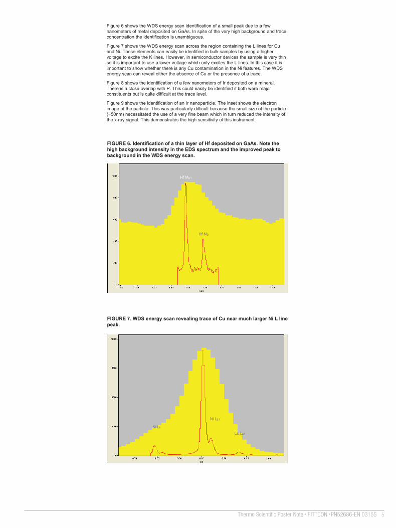
Figure 3 compares the EDS spectra for Mg Kɑ and As Lɑ. These two peaks are about 32 eV apart and their shapes are quite different. When each peak is of high intensity, as is shown here, then their identification is quite easy. EDS excels at this kind of application.
Figure 4 shows a minor peak at about the same energy. It is no longer obvious if this is from Mg, As or a combination of the two. The variance contributed from the relatively high background and the possibility of interfering signals from the other dominant peaks makes this identification very difficult.
Figure 5 shows the overlay of the WDS energy scan and the EDS spectrum of this minor peak. It is now obvious that the peak is due to a combination of Mg and As. Not only that, because of the extremely sharp resolution of the WDS spectrometer this data is useful to explain to others what was discovered here. Even readers unfamiliar with SEMs and x-ray spectroscopy can observe the presence of the labeled peaks.
Figure 6 shows the WDS energy scan identification of a small peak due to a few nanometers of metal deposited on GaAs. In spite of the very high background and trace concentration the identification is unambiguous.
Figure 7 shows the WDS energy scan across the region containing the L lines for Cu and Ni. These elements can easily be identified in bulk samples by using a higher voltage to excite the K lines. However, in semiconductor devices the sample is very thin so it is important to use a lower voltage which only excites the L lines. In this case it is important to show whether there is any Cu contamination in the Ni features. The WDS energy scan can reveal either the absence of Cu or the presence of a trace.
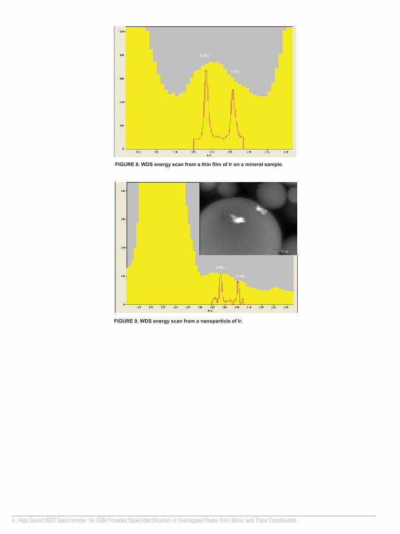
Figure 8 shows the identification of a few nanometers of Ir deposited on a mineral. There is a close overlap with P. This could easily be identified if both were major constituents but is quite difficult at the trace level.
Figure 9 shows the identification of an Ir nanoparticle. The inset shows the electron image of the particle. This was particularly difficult because the small size of the particle (~50nm) necessitated the use of a very fine beam which in turn reduced the intensity of the x-ray signal. This demonstrates the high sensitivity of this instrument.
Figure 2. Two views of the x-ray optic showing the outer mirror and the inner polycapillary.
Figure 1. Schematic of the spectrometer design. The x-ray optic converts diverging x-rays to a parallel beam. The detector counts x-rays which satisfy the Bragg condition for the angles determined by the crystal and the detector and the sample. The crystal rotates on its axis, the detector translates along a circular arc, the optic does not move.
FIGURE 3. Comparison of Mg K and As L peaks when both elements are major constituents in the sample (Mg(OH)2 and Lollingite)
FIGURE 4. Minor constituent which may be due to either Mg, As or both.
?
FIGURE 5. Unknown peak clearly identified by a WDS energy scan.
Mg KαAs Lα1
As Lβ1
FIGURE 6. Identification of a thin layer of Hf deposited on GaAs. Note the high background intensity in the EDS spectrum and the improved peak to background in the WDS energy scan.
Hf Mα1
Hf Mβ
FIGURE 7. WDS energy scan revealing trace of Cu near much larger Ni L line peak.
Ni Lα1
Ni Lβ1
Ni LλCu Lα1
FIGURE 9. WDS energy scan from a nanoparticle of Ir.
Ir Mα1
Ir Mβ
FIGURE 8. WDS energy scan from a thin film of Ir on a mineral sample.
Ir Mα1
Ir Mβ
All trademarks are the property of Thermo Fisher Scientific and its subsidiaries.
This information is not intended to encourage use of these products in any manners that might infringe the intellectual property rights of others.
3Thermo Scienti� c Poster Note • PITTCON • PN52686-EN 0315S
High Speed WDS Spectrometer for SEM Provides Rapid Identification of Overlapped Peaks from Minor and Trace ConstituentsJohn Konopka, Bill SgammatoThermo Fisher Scientific, Madison WI
ConclusionsA new design of a WDS spectrometer has been successfully engineered which brings the high resolving power of a wavelength dispersive spectroscopy to the regime of SEM/EDS. Non-experts using non-specialized electron microscopes now have access to this tool to complement their energy dispersive spectrometers.
References1. Woldseth, R. (1973) Everything You Wanted to Know About Xray Energy Dispersive
Spectrometry. p3.10, Burlingame: Kevex
2. Heinrich, K. F. J. (1981) Electron Beam X-ray Microanalysis. p104, New York: Van Nostrand.
OverviewA wavelength dispersive x-ray spectrometer (WDS) has been developed as a complement to an energy dispersive X-ray spectrometer (EDS).
The device was engineered to be extremely fast, easily used by a broad class of analysts and easily adapted to a wide range of scanning electron microscopes (SEM).
The result is a device that is almost as easy to use as EDS yet provides far higher spectral resolution, giving the analyst an improved tool for quickly identifying overlapped x-ray lines and locating x-ray lines arising from trace elements.
IntroductionEDS is an extremely versatile technique for x-ray spectroscopy in the SEM. It is largely insensitive to changes in sample height (i.e., working distance or topography) as well as being able to a observe a wide area of the sample.(1)
EDS detectors capture the entire spectrum in one acquisition. This has the advantage that the measurements for all elements are acquired under identical conditions.
Newer silicon drift detectors (SDD) are roughly an order of magnitude larger than detectors were at their inception. This is important as characteristic x-rays produced in the SEM are relatively rare. Many electrons strike the sample without producing acharacteristic x-ray, and many x-rays that are produced are not detected.
Finally, EDS is very easy to use, requiring almost no set-up before acquiring data. The one drawback is that the spectral resolution is less than optimum. The native width of an x-ray emission line is of the order of 1 electron volt (eV), while typical SDD resolution is of the order of 100 eV depending on the energy being measured.
To meet this need for better resolution a new kind of WDS instrument has been developed as a complement to the EDS spectrometer.
MethodsTraditional WDS instruments, whether dedicated electron microprobe (EMPA) instruments or those designed for use on smaller electron columns, have been employed for precision analysis and quantitative analysis. The primarily goal of the new WDS instrument is to provide high energy resolution to the EDS analyst as a qualitative tool.
The geometry of the instrument is shown in Figure 1. Traditional WDS instruments typically use a focusing geometry such as the Johansson spectrometer(2). This design produces a large design as both the diffracting crystal and the x-ray detector must move along a focusing circle depending on the energy being observed.
In the geometry of the newer WDS instrument there is no focusing circle. Rather, a focusing optic is used to convert the diverging x-rays from the sample to a parallel beam. The parallel beam is diffracted from a flat resolving crystal and measured by a detector. The detector rotates and moves in an arc to determine the Bragg angle for the wavelength of x-ray being measured.
Here the x-ray optic is a compound device comprised of a grazing incident parabolic cylindrical mirror and a polycapillary inside of that. The mirror is more effective focusing low energy x-rays below about 1.7 keV and the polycarpellary is more effective at focusing x-rays above 1.7 keV. The combined device provides full coverage of the x-ray spectrum from about 100 eV to over 10 keV.
A photograph of the optic is shown in Figure 2. The optic is maintained at the end of a tube near the sample.
The detector is a sealed, xenon-filled proportional device that requires no maintenance. Traditional WDS detectors used a flow proportional detector that requires a continuous supply of P10 gas.
Because of the simpler geometry only rotational motions are required. In this design one motor rotates the resolving crystal and one motor rotates the detector arm. These are direct drive motors with no belts, gears or pulleys.
Traditional WDS spectrometer systems require the operator to select some x-ray energy dependent values for the detector bias voltage and the single channel analyzer (SCA). In this system these parameters are managed by algorithms so that no user input is required to operate the system beyond selecting the energy range to measure.
ResultsThe resulting instrument meets the goals of being fast and simple when applied to qualitative analysis.
The system is extremely fast. It can change from one energy to another in less than 0.25seconds when using the same crystal. If a crystal change is required this occurs in less than 3 seconds.
The use of the x-ray optic provides a constant take off angle at all energies. This is usually designed to be the same take off angle as that of the EDS detector. The optic also provides a large solid angle. The small size of the optic and the large solid angle make it practical to install on nearly any SEM.
It can usually be mounted on the SEM chamber in a port designed for an EDS detector and does not require a specialized WDS port.
The system requires no other utilities than electricity. The instrument can be easily shut down in not needed for analysis.
The combination of the very fast, direct drive motors and the high sensitivity provided by the x-ray optic results in an instrument that can perform energy scans across x-ray emission peaks in a time comparable to those traditionally used to acquired a single EDS spectrum—about a minute.
As the optic has a focal point it must be aligned to point to where the electron beam strikes the sample. An automated routine performs this operation on demand.
Figure 3 compares the EDS spectra for Mg Kɑ and As Lɑ. These two peaks are about 32 eV apart and their shapes are quite different. When each peak is of high intensity, as is shown here, then their identification is quite easy. EDS excels at this kind of application.
Figure 4 shows a minor peak at about the same energy. It is no longer obvious if this is from Mg, As or a combination of the two. The variance contributed from the relatively high background and the possibility of interfering signals from the other dominant peaks makes this identification very difficult.
Figure 5 shows the overlay of the WDS energy scan and the EDS spectrum of this minor peak. It is now obvious that the peak is due to a combination of Mg and As. Not only that, because of the extremely sharp resolution of the WDS spectrometer this data is useful to explain to others what was discovered here. Even readers unfamiliar with SEMs and x-ray spectroscopy can observe the presence of the labeled peaks.
Figure 6 shows the WDS energy scan identification of a small peak due to a few nanometers of metal deposited on GaAs. In spite of the very high background and trace concentration the identification is unambiguous.
Figure 7 shows the WDS energy scan across the region containing the L lines for Cu and Ni. These elements can easily be identified in bulk samples by using a higher voltage to excite the K lines. However, in semiconductor devices the sample is very thin so it is important to use a lower voltage which only excites the L lines. In this case it is important to show whether there is any Cu contamination in the Ni features. The WDS energy scan can reveal either the absence of Cu or the presence of a trace.
Figure 8 shows the identification of a few nanometers of Ir deposited on a mineral. There is a close overlap with P. This could easily be identified if both were major constituents but is quite difficult at the trace level.
Figure 9 shows the identification of an Ir nanoparticle. The inset shows the electron image of the particle. This was particularly difficult because the small size of the particle (~50nm) necessitated the use of a very fine beam which in turn reduced the intensity of the x-ray signal. This demonstrates the high sensitivity of this instrument.
Figure 2. Two views of the x-ray optic showing the outer mirror and the inner polycapillary.
Figure 1. Schematic of the spectrometer design. The x-ray optic converts diverging x-rays to a parallel beam. The detector counts x-rays which satisfy the Bragg condition for the angles determined by the crystal and the detector and the sample. The crystal rotates on its axis, the detector translates along a circular arc, the optic does not move.
FIGURE 3. Comparison of Mg K and As L peaks when both elements are major constituents in the sample (Mg(OH)2 and Lollingite)
FIGURE 4. Minor constituent which may be due to either Mg, As or both.
?
FIGURE 5. Unknown peak clearly identified by a WDS energy scan.
Mg KαAs Lα1
As Lβ1
FIGURE 6. Identification of a thin layer of Hf deposited on GaAs. Note the high background intensity in the EDS spectrum and the improved peak to background in the WDS energy scan.
Hf Mα1
Hf Mβ
FIGURE 7. WDS energy scan revealing trace of Cu near much larger Ni L line peak.
Ni Lα1
Ni Lβ1
Ni LλCu Lα1
FIGURE 9. WDS energy scan from a nanoparticle of Ir.
Ir Mα1
Ir Mβ
FIGURE 8. WDS energy scan from a thin film of Ir on a mineral sample.
Ir Mα1
Ir Mβ
All trademarks are the property of Thermo Fisher Scientific and its subsidiaries.
This information is not intended to encourage use of these products in any manners that might infringe the intellectual property rights of others.
4 High Speed WDS Spectrometer for SEM Provides Rapid Identi� cation of Overlapped Peaks from Minor and Trace Constituents
High Speed WDS Spectrometer for SEM Provides Rapid Identification of Overlapped Peaks from Minor and Trace ConstituentsJohn Konopka, Bill SgammatoThermo Fisher Scientific, Madison WI
ConclusionsA new design of a WDS spectrometer has been successfully engineered which brings the high resolving power of a wavelength dispersive spectroscopy to the regime of SEM/EDS. Non-experts using non-specialized electron microscopes now have access to this tool to complement their energy dispersive spectrometers.
References1. Woldseth, R. (1973) Everything You Wanted to Know About Xray Energy Dispersive
Spectrometry. p3.10, Burlingame: Kevex
2. Heinrich, K. F. J. (1981) Electron Beam X-ray Microanalysis. p104, New York: Van Nostrand.
OverviewA wavelength dispersive x-ray spectrometer (WDS) has been developed as a complement to an energy dispersive X-ray spectrometer (EDS).
The device was engineered to be extremely fast, easily used by a broad class of analysts and easily adapted to a wide range of scanning electron microscopes (SEM).
The result is a device that is almost as easy to use as EDS yet provides far higher spectral resolution, giving the analyst an improved tool for quickly identifying overlapped x-ray lines and locating x-ray lines arising from trace elements.
IntroductionEDS is an extremely versatile technique for x-ray spectroscopy in the SEM. It is largely insensitive to changes in sample height (i.e., working distance or topography) as well as being able to a observe a wide area of the sample.(1)
EDS detectors capture the entire spectrum in one acquisition. This has the advantage that the measurements for all elements are acquired under identical conditions.
Newer silicon drift detectors (SDD) are roughly an order of magnitude larger than detectors were at their inception. This is important as characteristic x-rays produced in the SEM are relatively rare. Many electrons strike the sample without producing acharacteristic x-ray, and many x-rays that are produced are not detected.
Finally, EDS is very easy to use, requiring almost no set-up before acquiring data. The one drawback is that the spectral resolution is less than optimum. The native width of an x-ray emission line is of the order of 1 electron volt (eV), while typical SDD resolution is of the order of 100 eV depending on the energy being measured.
To meet this need for better resolution a new kind of WDS instrument has been developed as a complement to the EDS spectrometer.
MethodsTraditional WDS instruments, whether dedicated electron microprobe (EMPA) instruments or those designed for use on smaller electron columns, have been employed for precision analysis and quantitative analysis. The primarily goal of the new WDS instrument is to provide high energy resolution to the EDS analyst as a qualitative tool.
The geometry of the instrument is shown in Figure 1. Traditional WDS instruments typically use a focusing geometry such as the Johansson spectrometer(2). This design produces a large design as both the diffracting crystal and the x-ray detector must move along a focusing circle depending on the energy being observed.
In the geometry of the newer WDS instrument there is no focusing circle. Rather, a focusing optic is used to convert the diverging x-rays from the sample to a parallel beam. The parallel beam is diffracted from a flat resolving crystal and measured by a detector. The detector rotates and moves in an arc to determine the Bragg angle for the wavelength of x-ray being measured.
Here the x-ray optic is a compound device comprised of a grazing incident parabolic cylindrical mirror and a polycapillary inside of that. The mirror is more effective focusing low energy x-rays below about 1.7 keV and the polycarpellary is more effective at focusing x-rays above 1.7 keV. The combined device provides full coverage of the x-ray spectrum from about 100 eV to over 10 keV.
A photograph of the optic is shown in Figure 2. The optic is maintained at the end of a tube near the sample.
The detector is a sealed, xenon-filled proportional device that requires no maintenance. Traditional WDS detectors used a flow proportional detector that requires a continuous supply of P10 gas.
Because of the simpler geometry only rotational motions are required. In this design one motor rotates the resolving crystal and one motor rotates the detector arm. These are direct drive motors with no belts, gears or pulleys.
Traditional WDS spectrometer systems require the operator to select some x-ray energy dependent values for the detector bias voltage and the single channel analyzer (SCA). In this system these parameters are managed by algorithms so that no user input is required to operate the system beyond selecting the energy range to measure.
ResultsThe resulting instrument meets the goals of being fast and simple when applied to qualitative analysis.
The system is extremely fast. It can change from one energy to another in less than 0.25seconds when using the same crystal. If a crystal change is required this occurs in less than 3 seconds.
The use of the x-ray optic provides a constant take off angle at all energies. This is usually designed to be the same take off angle as that of the EDS detector. The optic also provides a large solid angle. The small size of the optic and the large solid angle make it practical to install on nearly any SEM.
It can usually be mounted on the SEM chamber in a port designed for an EDS detector and does not require a specialized WDS port.
The system requires no other utilities than electricity. The instrument can be easily shut down in not needed for analysis.
The combination of the very fast, direct drive motors and the high sensitivity provided by the x-ray optic results in an instrument that can perform energy scans across x-ray emission peaks in a time comparable to those traditionally used to acquired a single EDS spectrum—about a minute.
As the optic has a focal point it must be aligned to point to where the electron beam strikes the sample. An automated routine performs this operation on demand.
Figure 3 compares the EDS spectra for Mg Kɑ and As Lɑ. These two peaks are about 32 eV apart and their shapes are quite different. When each peak is of high intensity, as is shown here, then their identification is quite easy. EDS excels at this kind of application.
Figure 4 shows a minor peak at about the same energy. It is no longer obvious if this is from Mg, As or a combination of the two. The variance contributed from the relatively high background and the possibility of interfering signals from the other dominant peaks makes this identification very difficult.
Figure 5 shows the overlay of the WDS energy scan and the EDS spectrum of this minor peak. It is now obvious that the peak is due to a combination of Mg and As. Not only that, because of the extremely sharp resolution of the WDS spectrometer this data is useful to explain to others what was discovered here. Even readers unfamiliar with SEMs and x-ray spectroscopy can observe the presence of the labeled peaks.
Figure 6 shows the WDS energy scan identification of a small peak due to a few nanometers of metal deposited on GaAs. In spite of the very high background and trace concentration the identification is unambiguous.
Figure 7 shows the WDS energy scan across the region containing the L lines for Cu and Ni. These elements can easily be identified in bulk samples by using a higher voltage to excite the K lines. However, in semiconductor devices the sample is very thin so it is important to use a lower voltage which only excites the L lines. In this case it is important to show whether there is any Cu contamination in the Ni features. The WDS energy scan can reveal either the absence of Cu or the presence of a trace.
Figure 8 shows the identification of a few nanometers of Ir deposited on a mineral. There is a close overlap with P. This could easily be identified if both were major constituents but is quite difficult at the trace level.
Figure 9 shows the identification of an Ir nanoparticle. The inset shows the electron image of the particle. This was particularly difficult because the small size of the particle (~50nm) necessitated the use of a very fine beam which in turn reduced the intensity of the x-ray signal. This demonstrates the high sensitivity of this instrument.
Figure 2. Two views of the x-ray optic showing the outer mirror and the inner polycapillary.
Figure 1. Schematic of the spectrometer design. The x-ray optic converts diverging x-rays to a parallel beam. The detector counts x-rays which satisfy the Bragg condition for the angles determined by the crystal and the detector and the sample. The crystal rotates on its axis, the detector translates along a circular arc, the optic does not move.
FIGURE 3. Comparison of Mg K and As L peaks when both elements are major constituents in the sample (Mg(OH)2 and Lollingite)
FIGURE 4. Minor constituent which may be due to either Mg, As or both.
?
FIGURE 5. Unknown peak clearly identified by a WDS energy scan.
Mg KαAs Lα1
As Lβ1
FIGURE 6. Identification of a thin layer of Hf deposited on GaAs. Note the high background intensity in the EDS spectrum and the improved peak to background in the WDS energy scan.
Hf Mα1
Hf Mβ
FIGURE 7. WDS energy scan revealing trace of Cu near much larger Ni L line peak.
Ni Lα1
Ni Lβ1
Ni LλCu Lα1
FIGURE 9. WDS energy scan from a nanoparticle of Ir.
Ir Mα1
Ir Mβ
FIGURE 8. WDS energy scan from a thin film of Ir on a mineral sample.
Ir Mα1
Ir Mβ
All trademarks are the property of Thermo Fisher Scientific and its subsidiaries.
This information is not intended to encourage use of these products in any manners that might infringe the intellectual property rights of others.
5Thermo Scienti� c Poster Note • PITTCON • PN52686-EN 0315S
High Speed WDS Spectrometer for SEM Provides Rapid Identification of Overlapped Peaks from Minor and Trace ConstituentsJohn Konopka, Bill SgammatoThermo Fisher Scientific, Madison WI
ConclusionsA new design of a WDS spectrometer has been successfully engineered which brings the high resolving power of a wavelength dispersive spectroscopy to the regime of SEM/EDS. Non-experts using non-specialized electron microscopes now have access to this tool to complement their energy dispersive spectrometers.
References1. Woldseth, R. (1973) Everything You Wanted to Know About Xray Energy Dispersive
Spectrometry. p3.10, Burlingame: Kevex
2. Heinrich, K. F. J. (1981) Electron Beam X-ray Microanalysis. p104, New York: Van Nostrand.
OverviewA wavelength dispersive x-ray spectrometer (WDS) has been developed as a complement to an energy dispersive X-ray spectrometer (EDS).
The device was engineered to be extremely fast, easily used by a broad class of analysts and easily adapted to a wide range of scanning electron microscopes (SEM).
The result is a device that is almost as easy to use as EDS yet provides far higher spectral resolution, giving the analyst an improved tool for quickly identifying overlapped x-ray lines and locating x-ray lines arising from trace elements.
IntroductionEDS is an extremely versatile technique for x-ray spectroscopy in the SEM. It is largely insensitive to changes in sample height (i.e., working distance or topography) as well as being able to a observe a wide area of the sample.(1)
EDS detectors capture the entire spectrum in one acquisition. This has the advantage that the measurements for all elements are acquired under identical conditions.
Newer silicon drift detectors (SDD) are roughly an order of magnitude larger than detectors were at their inception. This is important as characteristic x-rays produced in the SEM are relatively rare. Many electrons strike the sample without producing acharacteristic x-ray, and many x-rays that are produced are not detected.
Finally, EDS is very easy to use, requiring almost no set-up before acquiring data. The one drawback is that the spectral resolution is less than optimum. The native width of an x-ray emission line is of the order of 1 electron volt (eV), while typical SDD resolution is of the order of 100 eV depending on the energy being measured.
To meet this need for better resolution a new kind of WDS instrument has been developed as a complement to the EDS spectrometer.
MethodsTraditional WDS instruments, whether dedicated electron microprobe (EMPA) instruments or those designed for use on smaller electron columns, have been employed for precision analysis and quantitative analysis. The primarily goal of the new WDS instrument is to provide high energy resolution to the EDS analyst as a qualitative tool.
The geometry of the instrument is shown in Figure 1. Traditional WDS instruments typically use a focusing geometry such as the Johansson spectrometer(2). This design produces a large design as both the diffracting crystal and the x-ray detector must move along a focusing circle depending on the energy being observed.
In the geometry of the newer WDS instrument there is no focusing circle. Rather, a focusing optic is used to convert the diverging x-rays from the sample to a parallel beam. The parallel beam is diffracted from a flat resolving crystal and measured by a detector. The detector rotates and moves in an arc to determine the Bragg angle for the wavelength of x-ray being measured.
Here the x-ray optic is a compound device comprised of a grazing incident parabolic cylindrical mirror and a polycapillary inside of that. The mirror is more effective focusing low energy x-rays below about 1.7 keV and the polycarpellary is more effective at focusing x-rays above 1.7 keV. The combined device provides full coverage of the x-ray spectrum from about 100 eV to over 10 keV.
A photograph of the optic is shown in Figure 2. The optic is maintained at the end of a tube near the sample.
The detector is a sealed, xenon-filled proportional device that requires no maintenance. Traditional WDS detectors used a flow proportional detector that requires a continuous supply of P10 gas.
Because of the simpler geometry only rotational motions are required. In this design one motor rotates the resolving crystal and one motor rotates the detector arm. These are direct drive motors with no belts, gears or pulleys.
Traditional WDS spectrometer systems require the operator to select some x-ray energy dependent values for the detector bias voltage and the single channel analyzer (SCA). In this system these parameters are managed by algorithms so that no user input is required to operate the system beyond selecting the energy range to measure.
ResultsThe resulting instrument meets the goals of being fast and simple when applied to qualitative analysis.
The system is extremely fast. It can change from one energy to another in less than 0.25seconds when using the same crystal. If a crystal change is required this occurs in less than 3 seconds.
The use of the x-ray optic provides a constant take off angle at all energies. This is usually designed to be the same take off angle as that of the EDS detector. The optic also provides a large solid angle. The small size of the optic and the large solid angle make it practical to install on nearly any SEM.
It can usually be mounted on the SEM chamber in a port designed for an EDS detector and does not require a specialized WDS port.
The system requires no other utilities than electricity. The instrument can be easily shut down in not needed for analysis.
The combination of the very fast, direct drive motors and the high sensitivity provided by the x-ray optic results in an instrument that can perform energy scans across x-ray emission peaks in a time comparable to those traditionally used to acquired a single EDS spectrum—about a minute.
As the optic has a focal point it must be aligned to point to where the electron beam strikes the sample. An automated routine performs this operation on demand.
Figure 3 compares the EDS spectra for Mg Kɑ and As Lɑ. These two peaks are about 32 eV apart and their shapes are quite different. When each peak is of high intensity, as is shown here, then their identification is quite easy. EDS excels at this kind of application.
Figure 4 shows a minor peak at about the same energy. It is no longer obvious if this is from Mg, As or a combination of the two. The variance contributed from the relatively high background and the possibility of interfering signals from the other dominant peaks makes this identification very difficult.
Figure 5 shows the overlay of the WDS energy scan and the EDS spectrum of this minor peak. It is now obvious that the peak is due to a combination of Mg and As. Not only that, because of the extremely sharp resolution of the WDS spectrometer this data is useful to explain to others what was discovered here. Even readers unfamiliar with SEMs and x-ray spectroscopy can observe the presence of the labeled peaks.
Figure 6 shows the WDS energy scan identification of a small peak due to a few nanometers of metal deposited on GaAs. In spite of the very high background and trace concentration the identification is unambiguous.
Figure 7 shows the WDS energy scan across the region containing the L lines for Cu and Ni. These elements can easily be identified in bulk samples by using a higher voltage to excite the K lines. However, in semiconductor devices the sample is very thin so it is important to use a lower voltage which only excites the L lines. In this case it is important to show whether there is any Cu contamination in the Ni features. The WDS energy scan can reveal either the absence of Cu or the presence of a trace.
Figure 8 shows the identification of a few nanometers of Ir deposited on a mineral. There is a close overlap with P. This could easily be identified if both were major constituents but is quite difficult at the trace level.
Figure 9 shows the identification of an Ir nanoparticle. The inset shows the electron image of the particle. This was particularly difficult because the small size of the particle (~50nm) necessitated the use of a very fine beam which in turn reduced the intensity of the x-ray signal. This demonstrates the high sensitivity of this instrument.
Figure 2. Two views of the x-ray optic showing the outer mirror and the inner polycapillary.
Figure 1. Schematic of the spectrometer design. The x-ray optic converts diverging x-rays to a parallel beam. The detector counts x-rays which satisfy the Bragg condition for the angles determined by the crystal and the detector and the sample. The crystal rotates on its axis, the detector translates along a circular arc, the optic does not move.
FIGURE 3. Comparison of Mg K and As L peaks when both elements are major constituents in the sample (Mg(OH)2 and Lollingite)
FIGURE 4. Minor constituent which may be due to either Mg, As or both.
?
FIGURE 5. Unknown peak clearly identified by a WDS energy scan.
Mg KαAs Lα1
As Lβ1
FIGURE 6. Identification of a thin layer of Hf deposited on GaAs. Note the high background intensity in the EDS spectrum and the improved peak to background in the WDS energy scan.
Hf Mα1
Hf Mβ
FIGURE 7. WDS energy scan revealing trace of Cu near much larger Ni L line peak.
Ni Lα1
Ni Lβ1
Ni LλCu Lα1
FIGURE 9. WDS energy scan from a nanoparticle of Ir.
Ir Mα1
Ir Mβ
FIGURE 8. WDS energy scan from a thin film of Ir on a mineral sample.
Ir Mα1
Ir Mβ
All trademarks are the property of Thermo Fisher Scientific and its subsidiaries.
This information is not intended to encourage use of these products in any manners that might infringe the intellectual property rights of others.
6 High Speed WDS Spectrometer for SEM Provides Rapid Identi� cation of Overlapped Peaks from Minor and Trace Constituents
High Speed WDS Spectrometer for SEM Provides Rapid Identification of Overlapped Peaks from Minor and Trace ConstituentsJohn Konopka, Bill SgammatoThermo Fisher Scientific, Madison WI
ConclusionsA new design of a WDS spectrometer has been successfully engineered which brings the high resolving power of a wavelength dispersive spectroscopy to the regime of SEM/EDS. Non-experts using non-specialized electron microscopes now have access to this tool to complement their energy dispersive spectrometers.
References1. Woldseth, R. (1973) Everything You Wanted to Know About Xray Energy Dispersive
Spectrometry. p3.10, Burlingame: Kevex
2. Heinrich, K. F. J. (1981) Electron Beam X-ray Microanalysis. p104, New York: Van Nostrand.
OverviewA wavelength dispersive x-ray spectrometer (WDS) has been developed as a complement to an energy dispersive X-ray spectrometer (EDS).
The device was engineered to be extremely fast, easily used by a broad class of analysts and easily adapted to a wide range of scanning electron microscopes (SEM).
The result is a device that is almost as easy to use as EDS yet provides far higher spectral resolution, giving the analyst an improved tool for quickly identifying overlapped x-ray lines and locating x-ray lines arising from trace elements.
IntroductionEDS is an extremely versatile technique for x-ray spectroscopy in the SEM. It is largely insensitive to changes in sample height (i.e., working distance or topography) as well as being able to a observe a wide area of the sample.(1)
EDS detectors capture the entire spectrum in one acquisition. This has the advantage that the measurements for all elements are acquired under identical conditions.
Newer silicon drift detectors (SDD) are roughly an order of magnitude larger than detectors were at their inception. This is important as characteristic x-rays produced in the SEM are relatively rare. Many electrons strike the sample without producing acharacteristic x-ray, and many x-rays that are produced are not detected.
Finally, EDS is very easy to use, requiring almost no set-up before acquiring data. The one drawback is that the spectral resolution is less than optimum. The native width of an x-ray emission line is of the order of 1 electron volt (eV), while typical SDD resolution is of the order of 100 eV depending on the energy being measured.
To meet this need for better resolution a new kind of WDS instrument has been developed as a complement to the EDS spectrometer.
MethodsTraditional WDS instruments, whether dedicated electron microprobe (EMPA) instruments or those designed for use on smaller electron columns, have been employed for precision analysis and quantitative analysis. The primarily goal of the new WDS instrument is to provide high energy resolution to the EDS analyst as a qualitative tool.
The geometry of the instrument is shown in Figure 1. Traditional WDS instruments typically use a focusing geometry such as the Johansson spectrometer(2). This design produces a large design as both the diffracting crystal and the x-ray detector must move along a focusing circle depending on the energy being observed.
In the geometry of the newer WDS instrument there is no focusing circle. Rather, a focusing optic is used to convert the diverging x-rays from the sample to a parallel beam. The parallel beam is diffracted from a flat resolving crystal and measured by a detector. The detector rotates and moves in an arc to determine the Bragg angle for the wavelength of x-ray being measured.
Here the x-ray optic is a compound device comprised of a grazing incident parabolic cylindrical mirror and a polycapillary inside of that. The mirror is more effective focusing low energy x-rays below about 1.7 keV and the polycarpellary is more effective at focusing x-rays above 1.7 keV. The combined device provides full coverage of the x-ray spectrum from about 100 eV to over 10 keV.
A photograph of the optic is shown in Figure 2. The optic is maintained at the end of a tube near the sample.
The detector is a sealed, xenon-filled proportional device that requires no maintenance. Traditional WDS detectors used a flow proportional detector that requires a continuous supply of P10 gas.
Because of the simpler geometry only rotational motions are required. In this design one motor rotates the resolving crystal and one motor rotates the detector arm. These are direct drive motors with no belts, gears or pulleys.
Traditional WDS spectrometer systems require the operator to select some x-ray energy dependent values for the detector bias voltage and the single channel analyzer (SCA). In this system these parameters are managed by algorithms so that no user input is required to operate the system beyond selecting the energy range to measure.
ResultsThe resulting instrument meets the goals of being fast and simple when applied to qualitative analysis.
The system is extremely fast. It can change from one energy to another in less than 0.25seconds when using the same crystal. If a crystal change is required this occurs in less than 3 seconds.
The use of the x-ray optic provides a constant take off angle at all energies. This is usually designed to be the same take off angle as that of the EDS detector. The optic also provides a large solid angle. The small size of the optic and the large solid angle make it practical to install on nearly any SEM.
It can usually be mounted on the SEM chamber in a port designed for an EDS detector and does not require a specialized WDS port.
The system requires no other utilities than electricity. The instrument can be easily shut down in not needed for analysis.
The combination of the very fast, direct drive motors and the high sensitivity provided by the x-ray optic results in an instrument that can perform energy scans across x-ray emission peaks in a time comparable to those traditionally used to acquired a single EDS spectrum—about a minute.
As the optic has a focal point it must be aligned to point to where the electron beam strikes the sample. An automated routine performs this operation on demand.
Figure 3 compares the EDS spectra for Mg Kɑ and As Lɑ. These two peaks are about 32 eV apart and their shapes are quite different. When each peak is of high intensity, as is shown here, then their identification is quite easy. EDS excels at this kind of application.
Figure 4 shows a minor peak at about the same energy. It is no longer obvious if this is from Mg, As or a combination of the two. The variance contributed from the relatively high background and the possibility of interfering signals from the other dominant peaks makes this identification very difficult.
Figure 5 shows the overlay of the WDS energy scan and the EDS spectrum of this minor peak. It is now obvious that the peak is due to a combination of Mg and As. Not only that, because of the extremely sharp resolution of the WDS spectrometer this data is useful to explain to others what was discovered here. Even readers unfamiliar with SEMs and x-ray spectroscopy can observe the presence of the labeled peaks.
Figure 6 shows the WDS energy scan identification of a small peak due to a few nanometers of metal deposited on GaAs. In spite of the very high background and trace concentration the identification is unambiguous.
Figure 7 shows the WDS energy scan across the region containing the L lines for Cu and Ni. These elements can easily be identified in bulk samples by using a higher voltage to excite the K lines. However, in semiconductor devices the sample is very thin so it is important to use a lower voltage which only excites the L lines. In this case it is important to show whether there is any Cu contamination in the Ni features. The WDS energy scan can reveal either the absence of Cu or the presence of a trace.
Figure 8 shows the identification of a few nanometers of Ir deposited on a mineral. There is a close overlap with P. This could easily be identified if both were major constituents but is quite difficult at the trace level.
Figure 9 shows the identification of an Ir nanoparticle. The inset shows the electron image of the particle. This was particularly difficult because the small size of the particle (~50nm) necessitated the use of a very fine beam which in turn reduced the intensity of the x-ray signal. This demonstrates the high sensitivity of this instrument.
Figure 2. Two views of the x-ray optic showing the outer mirror and the inner polycapillary.
Figure 1. Schematic of the spectrometer design. The x-ray optic converts diverging x-rays to a parallel beam. The detector counts x-rays which satisfy the Bragg condition for the angles determined by the crystal and the detector and the sample. The crystal rotates on its axis, the detector translates along a circular arc, the optic does not move.
FIGURE 3. Comparison of Mg K and As L peaks when both elements are major constituents in the sample (Mg(OH)2 and Lollingite)
FIGURE 4. Minor constituent which may be due to either Mg, As or both.
?
FIGURE 5. Unknown peak clearly identified by a WDS energy scan.
Mg KαAs Lα1
As Lβ1
FIGURE 6. Identification of a thin layer of Hf deposited on GaAs. Note the high background intensity in the EDS spectrum and the improved peak to background in the WDS energy scan.
Hf Mα1
Hf Mβ
FIGURE 7. WDS energy scan revealing trace of Cu near much larger Ni L line peak.
Ni Lα1
Ni Lβ1
Ni LλCu Lα1
FIGURE 9. WDS energy scan from a nanoparticle of Ir.
Ir Mα1
Ir Mβ
FIGURE 8. WDS energy scan from a thin film of Ir on a mineral sample.
Ir Mα1
Ir Mβ
All trademarks are the property of Thermo Fisher Scientific and its subsidiaries.
This information is not intended to encourage use of these products in any manners that might infringe the intellectual property rights of others.

PN52686-EN 0315S
High Speed WDS Spectrometer for SEM Provides Rapid Identification of Overlapped Peaks from Minor and Trace ConstituentsJohn Konopka, Bill SgammatoThermo Fisher Scientific, Madison WI
ConclusionsA new design of a WDS spectrometer has been successfully engineered which brings the high resolving power of a wavelength dispersive spectroscopy to the regime of SEM/EDS. Non-experts using non-specialized electron microscopes now have access to this tool to complement their energy dispersive spectrometers.
References1. Woldseth, R. (1973) Everything You Wanted to Know About Xray Energy Dispersive
Spectrometry. p3.10, Burlingame: Kevex
2. Heinrich, K. F. J. (1981) Electron Beam X-ray Microanalysis. p104, New York: Van Nostrand.
OverviewA wavelength dispersive x-ray spectrometer (WDS) has been developed as a complement to an energy dispersive X-ray spectrometer (EDS).
The device was engineered to be extremely fast, easily used by a broad class of analysts and easily adapted to a wide range of scanning electron microscopes (SEM).
The result is a device that is almost as easy to use as EDS yet provides far higher spectral resolution, giving the analyst an improved tool for quickly identifying overlapped x-ray lines and locating x-ray lines arising from trace elements.
IntroductionEDS is an extremely versatile technique for x-ray spectroscopy in the SEM. It is largely insensitive to changes in sample height (i.e., working distance or topography) as well as being able to a observe a wide area of the sample.(1)
EDS detectors capture the entire spectrum in one acquisition. This has the advantage that the measurements for all elements are acquired under identical conditions.
Newer silicon drift detectors (SDD) are roughly an order of magnitude larger than detectors were at their inception. This is important as characteristic x-rays produced in the SEM are relatively rare. Many electrons strike the sample without producing acharacteristic x-ray, and many x-rays that are produced are not detected.
Finally, EDS is very easy to use, requiring almost no set-up before acquiring data. The one drawback is that the spectral resolution is less than optimum. The native width of an x-ray emission line is of the order of 1 electron volt (eV), while typical SDD resolution is of the order of 100 eV depending on the energy being measured.
To meet this need for better resolution a new kind of WDS instrument has been developed as a complement to the EDS spectrometer.
MethodsTraditional WDS instruments, whether dedicated electron microprobe (EMPA) instruments or those designed for use on smaller electron columns, have been employed for precision analysis and quantitative analysis. The primarily goal of the new WDS instrument is to provide high energy resolution to the EDS analyst as a qualitative tool.
The geometry of the instrument is shown in Figure 1. Traditional WDS instruments typically use a focusing geometry such as the Johansson spectrometer(2). This design produces a large design as both the diffracting crystal and the x-ray detector must move along a focusing circle depending on the energy being observed.
In the geometry of the newer WDS instrument there is no focusing circle. Rather, a focusing optic is used to convert the diverging x-rays from the sample to a parallel beam. The parallel beam is diffracted from a flat resolving crystal and measured by a detector. The detector rotates and moves in an arc to determine the Bragg angle for the wavelength of x-ray being measured.
Here the x-ray optic is a compound device comprised of a grazing incident parabolic cylindrical mirror and a polycapillary inside of that. The mirror is more effective focusing low energy x-rays below about 1.7 keV and the polycarpellary is more effective at focusing x-rays above 1.7 keV. The combined device provides full coverage of the x-ray spectrum from about 100 eV to over 10 keV.
A photograph of the optic is shown in Figure 2. The optic is maintained at the end of a tube near the sample.
The detector is a sealed, xenon-filled proportional device that requires no maintenance. Traditional WDS detectors used a flow proportional detector that requires a continuous supply of P10 gas.
Because of the simpler geometry only rotational motions are required. In this design one motor rotates the resolving crystal and one motor rotates the detector arm. These are direct drive motors with no belts, gears or pulleys.
Traditional WDS spectrometer systems require the operator to select some x-ray energy dependent values for the detector bias voltage and the single channel analyzer (SCA). In this system these parameters are managed by algorithms so that no user input is required to operate the system beyond selecting the energy range to measure.
ResultsThe resulting instrument meets the goals of being fast and simple when applied to qualitative analysis.
The system is extremely fast. It can change from one energy to another in less than 0.25seconds when using the same crystal. If a crystal change is required this occurs in less than 3 seconds.
The use of the x-ray optic provides a constant take off angle at all energies. This is usually designed to be the same take off angle as that of the EDS detector. The optic also provides a large solid angle. The small size of the optic and the large solid angle make it practical to install on nearly any SEM.
It can usually be mounted on the SEM chamber in a port designed for an EDS detector and does not require a specialized WDS port.
The system requires no other utilities than electricity. The instrument can be easily shut down in not needed for analysis.
The combination of the very fast, direct drive motors and the high sensitivity provided by the x-ray optic results in an instrument that can perform energy scans across x-ray emission peaks in a time comparable to those traditionally used to acquired a single EDS spectrum—about a minute.
As the optic has a focal point it must be aligned to point to where the electron beam strikes the sample. An automated routine performs this operation on demand.
Figure 3 compares the EDS spectra for Mg Kɑ and As Lɑ. These two peaks are about 32 eV apart and their shapes are quite different. When each peak is of high intensity, as is shown here, then their identification is quite easy. EDS excels at this kind of application.
Figure 4 shows a minor peak at about the same energy. It is no longer obvious if this is from Mg, As or a combination of the two. The variance contributed from the relatively high background and the possibility of interfering signals from the other dominant peaks makes this identification very difficult.
Figure 5 shows the overlay of the WDS energy scan and the EDS spectrum of this minor peak. It is now obvious that the peak is due to a combination of Mg and As. Not only that, because of the extremely sharp resolution of the WDS spectrometer this data is useful to explain to others what was discovered here. Even readers unfamiliar with SEMs and x-ray spectroscopy can observe the presence of the labeled peaks.
Figure 6 shows the WDS energy scan identification of a small peak due to a few nanometers of metal deposited on GaAs. In spite of the very high background and trace concentration the identification is unambiguous.
Figure 7 shows the WDS energy scan across the region containing the L lines for Cu and Ni. These elements can easily be identified in bulk samples by using a higher voltage to excite the K lines. However, in semiconductor devices the sample is very thin so it is important to use a lower voltage which only excites the L lines. In this case it is important to show whether there is any Cu contamination in the Ni features. The WDS energy scan can reveal either the absence of Cu or the presence of a trace.
Figure 8 shows the identification of a few nanometers of Ir deposited on a mineral. There is a close overlap with P. This could easily be identified if both were major constituents but is quite difficult at the trace level.
Figure 9 shows the identification of an Ir nanoparticle. The inset shows the electron image of the particle. This was particularly difficult because the small size of the particle (~50nm) necessitated the use of a very fine beam which in turn reduced the intensity of the x-ray signal. This demonstrates the high sensitivity of this instrument.
Figure 2. Two views of the x-ray optic showing the outer mirror and the inner polycapillary.
Figure 1. Schematic of the spectrometer design. The x-ray optic converts diverging x-rays to a parallel beam. The detector counts x-rays which satisfy the Bragg condition for the angles determined by the crystal and the detector and the sample. The crystal rotates on its axis, the detector translates along a circular arc, the optic does not move.
FIGURE 3. Comparison of Mg K and As L peaks when both elements are major constituents in the sample (Mg(OH)2 and Lollingite)
FIGURE 4. Minor constituent which may be due to either Mg, As or both.
?
FIGURE 5. Unknown peak clearly identified by a WDS energy scan.
Mg KαAs Lα1
As Lβ1
FIGURE 6. Identification of a thin layer of Hf deposited on GaAs. Note the high background intensity in the EDS spectrum and the improved peak to background in the WDS energy scan.
Hf Mα1
Hf Mβ
FIGURE 7. WDS energy scan revealing trace of Cu near much larger Ni L line peak.
Ni Lα1
Ni Lβ1
Ni LλCu Lα1
FIGURE 9. WDS energy scan from a nanoparticle of Ir.
Ir Mα1
Ir Mβ
FIGURE 8. WDS energy scan from a thin film of Ir on a mineral sample.
Ir Mα1
Ir Mβ
All trademarks are the property of Thermo Fisher Scientific and its subsidiaries.
This information is not intended to encourage use of these products in any manners that might infringe the intellectual property rights of others.
Africa +43 1 333 50 34 0Australia +61 3 9757 4300Austria +43 810 282 206Belgium +32 53 73 42 41Brazil +55 11 3731 5140Canada +1 800 530 8447China 800 810 5118 (free call domestic)
400 650 5118
Denmark +45 70 23 62 60Europe-Other +43 1 333 50 34 0Finland +358 9 3291 0200France +33 1 60 92 48 00Germany +49 6103 408 1014India +91 22 6742 9494Italy +39 02 950 591
Japan +81 6 6885 1213Korea +82 2 3420 8600Latin America +1 561 688 8700Middle East +43 1 333 50 34 0Netherlands +31 76 579 55 55 New Zealand +64 9 980 6700 Norway +46 8 556 468 00
Russia/CIS +43 1 333 50 34 0Singapore +65 6289 1190Sweden +46 8 556 468 00 Switzerland +41 61 716 77 00Taiwan +886 2 8751 6655UK/Ireland +44 1442 233555USA +1 800 532 4752
www.thermoscientific.com©2015 Thermo Fisher Scienti� c Inc. All rights reserved. ISO is a trademark of the International Standards Organization. All other trademarks are the property of Thermo Fisher Scienti� c and its subsidiaries. This information is presented as an example of the capabilities of Thermo Fisher Scienti� c products. It is not intended to encourage use of these products in any manners that might infringe the intellectual property rights of others. Speci� cations, terms and pricing are subject to change. Not all products are available in all countries. Please consult your local sales representative for details.
Thermo Fisher Scienti� c,San Jose, CA USA is ISO 9001 Certi� ed.