Embed Size (px)
Citation preview

HIGH TEMPERATURE CONDUCTIVITY OF GROWN
STANNIC OXIDE SINGLE CRYSTALS
By
HOWARD FRANKLIN KUNKLE JR. Ci
Bachelor of Arts Washington.and Jefferson College
Washit'\gton, Pennsylvania 1959
Master of Science Oklahoma State University
Stillwater, Oklahoma 1961
Submitted to the Faculty of the Graduate School of the Oklahoma State University
in partial fulfiilment of the requirements for the degree of
DOCTOR OF PHILOSOPHY May, 1966
CORE Metadata, citation and similar papers at core.ac.uk
Provided by SHAREOK repository

HIGH TEMPERATURE CONDUCTIVITY OF GROWN
STANNIC OXIDE SINGLE CRYSTALS
Thes;BA~-~
Thesis Adviser ·
6101~,

This research was supported by the
Office· of Naval .·Research under
Contract No. Nonr-2595(01)
iii

ACKNOWLEDGMENT
The author wishes to express his deepest gratitude to Dr. E. E.
Kohnke for· his patience and guidance throughout the execution of thi.s
work, to the Office of Naval Research for -sponsoring the research, to
the U.S. Department·of Health, Education and Welfare for financial
aid in the form of an N.D.E.A. Fellowship and to the Oklahoma State
University Research Foundation for·their administrative assistance. He
i · is also '.indebted to H. Hall and.W. Adkins for their·help with the design
and construction of experimental equipment, to Dr. J. Yahia and Dr. J.E.
Houston for their helpful suggestions and stimulating discussion, and to
Dr. R. Freeman for the loan of equipment. And finally the author .wishes
to recognize his wife, Garol, as his inspiration and for·her labor in
typing and proofreading.
iv

· Chapter
r.
II.
·III.
IV.
v.
VI.
TABLE OF CONTENTS
INTRODUCTION •••••
Metal Oxides Tin Oxide Review •••• Scope of the Present Study
. . . . . . . .
. . . .
CRYSTAL GROWTH AND IDENTIFICATION • • • • • • • •
Background on·oxide Growth in General • Tin Oxide· Growth • • • • • ·• • • • • • • • • • Impurity Analysis • . • .••• Crystal Identification •••••• Cryst;al Orientation. , • . • •
THEORETICAL ~ACK.GROUND.~
Electrical Conductivity. Thermoelectric Power
. . . . . . . . . . . . . . • •
SAMPLES, APPARATUS AND EXPERIMENTAL TECHNIQUE ·'1. . . ' .
Page
1
1 3 4
6
6 10 18 19 23
35
35 44
46
· Samples • ~ . . • • . . . • . . . . . . • . 46 . Apparatus . • . . . . . . . . . . . • . . . . . . . 49 Measuring_. Techniques • • • • • • • • • • · 59
RESULTS . . . . . . . . . . • • •
Introductory Remarks •••••• , , , , , , , • , Conductivity Results - Atmospheric Pressur.e • Vacuum Conductivity, , •••• . . . ~ Optical Absorption .. , • • • Thermoelectric Power Results • , • ,
DISCUSSION OF.RESULTS
Suggestions for Further Study,
• •
69
69 69 74 83 89
94
105
BIBLIOGRAPHY 109
APPENDIX , • . ~ . . . . 113
v

LIST OF TAB.LES
Table
r.. Comparison of Line Intersities and dhkl from Sn02 Powder Patterns by Various Authors • • • •
II. dhkl Values and Bragg Angles Calculated from Sno 2 Powder Pattern •••••••••••
IIL Comparison of Back Reflection Doublets Using Their Corresponding Wavelength Calculated.from Sno2 Powder Pattern •••••••••••
IV. Angles Between Crystallographic Planes Responsible
Page
25
26
27
for Prominent Spots in Figures 6 and 7 • • • • . • 30
v.
Figure
1.
2,
3.
4.
5.
Lattice Directions Indicated on Figures 6, 7 and 8 and Their Associated Angles •.•••••
LlST-oF FIGURES
Arrangement of Crucibles in the Furnace for VaporPhase Growth Technique , •• , ••••
Flux Growth Apparatus Schematic Diagram
X-ray Powder Photograph Camera ••
X-ray Powder Pattern Photograph of Flux-Grown Sno2 Crystals . . . . • . . . . • . . . . · .
Laue Back-reflection Technique Schematic Diagram.
. 6. Laue Back-reflection Photograph Taken in the Q.lQ) Direction . . . . . .. . . . . . . . .
7. Laue Back-reflection Photograph Taken in the [100] Direction
8. Laue Back-reflection Photograph Taken in the [OO(J Direction
9. Holder for Lapping Ends of Samples •
10. Bell Jar Apparatus for Conductivity Measurements •
vi
34
Page
11
14
20
24
28
. . . . 31
32
33
48
50
Figure Page
11. Crystal Holder·for Conductivity Measurements • 51
12. Quartz Furnace Design for Conductivity Measurements 52
13. Portable Vacuum System Schematic Diagram. . ,, . 54
14. Apparatus for Thermocouple Comparison 56
15. Crystal Holder for.Thermoelectric Power. Measurements • 58
16. Crystal Holder·for ~easuring'.4..:Probe Conductivity •••• 60
17. Typical Crystal Current:as a Function of Voltage 63
18. Block Diagram of Conductivity Measuring ·Circuit· 65
·19. Block Diagram of Thermoelectric Power Measuring'Circu:i.t. • 67
·20. Crystal Current as. a Function of Reciprocal Temperature · for Several "Fixing" pemperatures • • • • • ·• • • • • • 70
.21. Crystal Current Data Showing Reproducibility Below a Fixing Temperature • . • • • • • • • • • • • .. • • • 72
22. Thermally Stimulated Current as a Function of Reciprocal Temperature • • • • • • • • • • • • • • • • • 73
23. Crystal Curre1;1t Versus Reciprocal Temperature for One Fixing Temperature at Various Pressures • • • • • 75
2~.
25.
26.
27.
28.
29.
30.
31.
Crystal ·current lsotherms Versus Pressure •••
Crystal Current· as a Function .. of· Time' from Temperature Decrease.at 10-2 Torr •••••••••••• ~ •••
Crystal Current as a Function-of Time from Temperature Increase at 10-2 Torr ••••••••••••••••
Crystal Current Versus Reciprocal Temperature.Showing Effect of Vacuum Fixing •••••••••••
.. .
Crystal Current Versus Reciprocal Temperature at One Pressure·for Various Fixing Temperatures ••••••••
Crystal Current Versus Reciprocal Temperature for Abraded.Surface Crystal •••••••••••••
Optical Transmission Comparison of Natural to Flux-Grown Sno2 Crystals • • . • • • • • • •
Optical Transmission Showing Fixing Effect.on 6 to.8 Micron Structure ••••••••••••••• ~ ••••
vii
76
77
79
80
81
84
85

Figure
32.
·33.
.34.
.35.
36.
Optical 'Iransmission Shqwing Visible:Wavelength ·Absorptions • • • • • • • • • • • • • •
Optical Transmission-of Vapor-Grown Sno2 Crystal in the Visible Wavelength Range ••••• ' •• -•••
Thermoelectric Power Versus Temperature for a High ·Temperature Fix • .- .• ·• • • • • • • • • • • • •
Thermoelectric Power Vers~s Temperature for Various Fixing Treatments • • • • • ••••••
Comparison of Thermoelectric Power and Conductivity for a High Temperature Fix •••••••
viii
Page
87
88
90
92
93

CHAPTER I
INTRODUCTION
Metal Oxides
Although'a vast amount of experimental work has been dene on metal
exides, there still exists considerable confusien as to their fundamental
electrical properties. This is understandable under the circumstances
since,overall sample preparation of oxides is difficult and the effects
of past· thermal and mechanical treatment. are increasingly recegni,,ed as
playing a significant role in property determination. Past investigations
have been scattered aver many forms of sp0ecimens, i.e., pressedpowqers,
sintered ceramics, polycrystalline thin films, crystalline thinfiims,
natural and synthetic sin.gle crystals. Reviews of typical work c-an be
1 2 3 found in, articles by Verwey · and Gray ' • It now seems reasonable to
hppe that with refined growth techniques p·roviding single crystals of
centrelled purity, work on exides in general will soon preduce a degree
o:1; understanding comparable to that which now exists for germanium and
silican.
Inthe past decade, efforts in the.area af crystal g;owth have
become more fruitful in the exides as well as in metals, arganic semi-
conductars, and intermetallic compeunds. Oxide crystal growth has, in
geneX"al, praperties that distinguish it .from athergrowth and which
require. special methods as well as equipment.- These can be mostly
attributed to the fact that oxides have highmelting points usually
1

2
ab.ova 1000°c - .. making it hard to find mater~als for crucibles and
furt_1aces. Further complications such.as partial decemposition or
eyaporation of the·material xp.ay. rule out certain standard growth tech~
niques. As·a result of these difficulties, controlled sample purity has
been.very hard to,attain. However, the list of available research· grade
oxide crystals has been·growing.at an.accelerated rate.
· A signiUcant portion of .the electrical work- <m oxides has been
done onTi02 4 and Zno 5 Others widely studied have been NiO, CuO,
Cu20 and Si02 as well as the refractory~oxides. Of particular perti-
nence tothe·work,desc:ribed in this report is the fact that another
rutile structure oxide, Sno2 has been studied in.a number of sample forms.
A review is presented in, the next section of this .chapter.
In, investigating the electrical properties of solids it is found
that both the·bulkand surface influence the results. It therefore.be-
.comes desirable to separate their individual centributions by specific
experiments or experimental techniques. One method is to regulate the
size of the sample such that different surface.:..to-volume ratios can be
examined. Anether is to note the·result. of gaseous ambient changes which
would be -expected to have their principal effect on, surfac:e--sensitive
properties. It has been noted that adsorption of gas en ·.exide surtaces
6 · 7 affec.ts such ·things as photo-conductive response , dark conductivity · and
.catalytic: activity8~ He1,,1ever, most of the work.in this area has been done
on· pressed:powders and/or ceramics cha;racterized by-large surface.areas.
It seems reasonable to suspect tl).at simi.la;t" .surface control ·of
electrical proper.ties· can exist in high purity· single crystals· having
. large forbidden energy gaps. and evidence will be prese-nted later in this
report showing that this .is true in the case of flux;..gr.01,,1n Sno2 crystals.

3
Tin Oxide Review
Sn02 , the main constituent of natural tin ore, is the material about
which this study is center~d. It has a bipyramidal ditetragonal crystal
structure with lattice dimensions of a= 4. 73727'J... and c= 3 .186383R 9 • In
· its natural crystalline form it is called cassiterite •. Thin films have
10 11 been investigated by Bauer and Fisher who reported resistivities of
10-2 ohm-cm, 6 c1ii2/volt .. sec for Hall mobility and 1020 cm-3 for free
election concentration. From dark C(:>nductivity vs temperature their
results indicated·activation energies of 0.02 ev near 100°K and 0.05 ev
12 near room temperature. Films were also studied by Ishiguro et al.,
h d 10- 2 hm 15 35 2/ 1 d 1·019 to.· 1020 .cm-3 f w o reporte ·· o . -cm, ;,.. cm vo t-sec an or
resistivity, mobility and electron concentration respectively. Le Blanc
13 and Sachse have reported resistivities for sintered samples of around
108 ohm.;.cm at roomtemperature whereas reports on pressed powders and
sintered samples by Guillery14 gave 104 to 108 ohm.,.cm at low temperatures.
After spraying SnC14 onto a hot substrate to. get a thin film of Sno2 ,
Miloslavskii15 obtained activation energies of 0.12 ev from conductivity
data in the temperature range from 150°C to 200°c, room temperature
re.sistivities from 102 to 103 ohm~cm. and electron densities of 1019 to
1020 . -3 cm
16 Foex , working with pressedpowder prepared by precipitating
Sno2 from.an acid solution and heat treating it in air at 1200°c, obtained
data that can be ~nalyzed to calculate. activation energie~ of 0.77 ev and
a forbidden gap of 4.0 ev in the 20°c to 1200°c temperature range. Kohnke17
reports values of 0.72 ev for natural crystalline samples of Sno2 having
14 15 . 3 10 -10 carriers/cm at room temperature. From·the short wavelength
cutoff intransmissi0n data he reports a gap of 3.54 ev compared to that
gotten from the maximum af the photoconductivity spectral response data

4
18 19 of 3.44 ev 1:>y Hurt • Loch compares some of the results of mobility in
sintered cold pressed powders with those al:>ove showing reasonable agreement.
Work has seen limited on synthetic Sno2 crystals due to lack of
samples. Reed and Roddy20 report having grown sample size Sno2 using a
21 vapor growth technique •. MacAvoy and Marley using a more refined system
' have produced good·.quality specimens. The result ef their electrical
measurements on grown samples will be reserved until later for comparison
22 purposes. Rous.ton has recently completed a comprehensive photo-
electronic analysis of flux.;.grown crystals produced locally. He pro-
p.oses an energy scheme for as-grown samples, reporting donor levels at
0.21, 0.50, 0.60, 1.00, 1.30 and 1.80 ev below the conduction band and
·an,accepter·level at 0.33 ev.above·the valence band. He reports also
that the 0.21 and 0.50 evlevels are totally compensated whereas the
0.60 ev level appears to be only partially compensated. These results
are further substantiated by dark conductivity measurements.
Scope of the Present Study
The results of a threefold investigation.are presented in these
pages. First, a method of growing sample~size synthetic crystals frama
cu2o flux is described. Secondly, optical studies werel'!lade on these
crystals and encompassed transmission measurements from the intrinsic
cutaff to 9 microns for comp.arisen with patural samples. A Polarizing
microscope was used in conjunction-with X-ray studies for identificatian
and orientatian purposes. Further optical wark was coupled with dark
cc:mductivity results to investigate the source of certain transmission
spectrum· changes in the 6 to 8 micron wavelength range. The third cate-
· gory involves a dark conductivity .and thermoelectric power ar,;alysis.

,5
Due to the geometry and purity 0f .these crystals, their cen,ciuctivity was
found to be surface contrelled. Hence the at').alysis has been intentionally
directed toward emphasizing the effect of surface conditiens on the con
duction process.
The results and their various implications are· used te. pr.epose. a
mCi>del explaining the phenomena noted on these crystals. It is so con
structed as to include all WCi>rk to date on flux-grown samples and tCi>
serve.as·a source <:>f suggestions for future work.

CHAPTER II
CRYSTAL GROWTH AND IDENTIFICATION
Background on Oxide Growth in General
In the past ten to fifteen years much effort has been concentrated
in the area of crystal growthwith the result that it now forms the basis
of a rather large industry. As mentioned before, the growth of oxide
crystals provides particular challenges which may necessitate the in-
· vent ion of new as well as the remodeling of old growth techniques.
In·general, crystal growth can be accomplished by the following
methods:
( 1) Solid polycrystal --+ solid single crystal or polycrystal, of larger grain size
(2) Gas ---,. Crystal
(3) Melt---+ Crystal
(4) Chemical reaction---,,+ Crystal
(5) S0lution __. Crystal
An example of method (1) is the grain growth which 0ccurs during the
annealing of cold--workedmetals. Alth0ugh it has been used for gr0wth
0f certain single crystals, this method l;las not·as yet been used f0r
oxides. Some oxides have been grown by .a technique classified as either
method.(2) or (4), which means the mechanism for the growth is not clearly
understood. Vapor-phase growth falls int0 one or the other of these cat-
egories. When it involves transport bya carrier gas from the metal to
crystal oxides it is definitely·(4), butwhen·the starting composition
6

7
or nutrient is the oxide itself in polycrystalline form both methods are
possible.at the same time. Since a good many oxides decompose before
they melt, method (4) is particularly inviting because growth in the
oxide form is possible in.a temperature range in which the oxide is a
stable composition.
Of all the methods, (3) is the most desirable ~ince in this case
only one constituent is presentand the possibilities of contamination
,are gr~atly reduced. With oxides this method has its problems since
melting points are usually high and crucible materials and furnaces
capable of withstanding high·temperatures and caustic ambients.are.at a
premium. Recently commercial units for extremely high temperatures have
been developed. In. cases where i_~duction heating is possible and the
crucible can be made of the material to be melted, instrumentation
problems are more easily overcome.
If an.added component does not interact strongly with the crystal
but does permit it to grow at a temperature below its melting point, it
is convenient to consider growth from solution, method (5). Such growth
may occur at normal temperatures and pressures or, as in hydrothermal
crystal growth, at rather high temperatµres and pressures. The solvent
may be water, an inorganic salt, or an oxide.at or above its melting point.
Some of the more prominent modifications of the.above :qamed methods
will be discussed in terms of their direct applicability to oxide growth.
Consider for example the Czochralski, or crystal pulling techniques.
This is cataloged under the heading of method (3) and has been used to
grow crystals of silicon and germanium, as well as the tungstates and
molybdates of calcium and strontium. The apparatus consists of a furnace
usually induction heated -- a noble metal crucible of platinum, gold or

rhodium holding the ·melt, and a seed which is normally ·rotated. The
·mech,anically_rotated seed. is slowly withdrawn from-the·melt and since
8
· the ··temperature· falls off sharply above the ·crucible, the, liquid. freezes
on ·the seed as it: i.s extracted. By controlling a variety of parameters
such as temperature-profile, pulling::rate, pulling_:direction and melt
purity, single crystals can be produced. If it is desired. to dope ·the
· crystal using· this method the·· oxide of the dopant. is added in ·the· proper
ratio-to the-melt. This method has the·possibility of an added .modi-
fication -~hich ·may. have usefulness in the near future;. pulling·.· from a
. flux melt .. instead of· the ·crystal melt. iiself. By using the proper
combination of solvent to ,solute, good crystal growth .. can ·occur ·pr9-
vided the solvent.has a high -separation .coefficient, i.e., provided
.that it will produce very little contamination.
The .. second. of four methods important : for oxides in general and. one
.which will be referred to.: later .with. regards to stannic oxide in partic
ular, is that of.· hydrothermal growth. The essential constituents are
·the-pressure vessel, solvent, seeqs, nutrient-and furnace. Usually
the nutrient·hasthe.same·composition as the seed and is placed in the
bottom of the pressure vesseL The· bomb is cylindrical. in shape and has
seeds hanging along· i1~s axis. By ·controlling solvent concentration,
primarily hydroxide-solution, and proper temperature,gradient along the
pressure·vessel,-the,seeds will be washed.with the·dissolved nutrient
into •the gro.wth .. zone of the cylinder and crystal growth ·can ·occur. For
quartz crystal gro,wth, a typical der:i.sity·of solvent .at·400°Cis 0.8 g/cc
which. ·.can produce· pressures in the· bomb. of 20, 000 p. s ~ i.
A third technique is that of growing-oxides from .. the vapor-phase
,which, as was stated previously, can be considered under ·either-method

9
(2) or (4) depending on the mechanism for growth. Apparatus in this case
can be varied but usually consists of a tube furnace capable of controlled
axial temperature gradients. The furnace tube is divided.into. two ~ones,
the growth zone.and the nutrient zone. In the nutrient zone.powder of
the same composition. as 1the crystals to be grown is heated to a temper-
.ature at which either decomposition occurs or the vapor pressure.approaches
atmospheric. A carrier gas made of a combination of·an inert gas such
.as nitrogen. or helium with oxygen is blown over the nutrient transport-
ing the growth constituents to the growth zone where either seeds are
placed or nucleation of seeds occurs naturally. This z.one is at a sub-
stantially lower temperature and is regulated to cause recrystallization.
Again, as is the case for most crystal growing techniques, many variables
must be controlled in order to get desired results. In many cases enly
a few combinations of these variables can produce sizeable crystal
growth to say nothing, of achieving nearly imperfection-free samples.
Another method with widespread use in the oxide growth in4ustry
is the Verneuil, or flame fusion technique. Powder of the crystal to be
grown is peure.d through an oxyQhydrogen flame and is melted. The flame
is focussed on.a seed crystal which is slowly lowered·as growth occurs,
producing in some cases large boules of crystals. Varied purity can
be attained depending on the purity.and composition of the starting powder.
This concludes a cursory review of the methods used for oxide growth
in general. However, these with their various modifications provide
·the bulk of oxide growth techniques. A review of the literature shows
tllat anyone crystal can usually be grown in a variety of ways. ·A good
1 . Z O h" h h b b h · 23 f examp e is n w 1c as een grown y vapor-p ase reaction , rom.a
24 25 flux melt of lead fluoride , and by a hydrothermal process • Other

10
examples are contained in the following list which is by no means
complete.
Vapor-phase grovrth: , 23 20,21
ZnO ·, Sn02
~elt or flux growth: Al203 28' Zri024 Sn~23 l' Fe2· 03 2;.ii'. . ' ~ .
. Hydrothermal growt,h: 25 32 . 33 30 32 ZnO , . Sn02 , 81.02 Al203 . , Geo2
Vertleuil growth: Tio226 , A1 2o327 (Sapphire)
Tin Oxide Growth
Within the past four years stannic oxide, Sno2 , has been grown by
20,21 31 . 32 three· methods, vapor .. phase · , flux , and hydrothermal This labo-
ratory investigated all three with positive results in two of the tech-
niques.
34 Vapor-Phase Growth - A vapor'"phase growth technique suggested by Reed
is a simplification of the method described in the previous section. It
used.a quartz container approximately two inches in diameter with one
closed·end·and the other connected to a one-quarter inch diameter chimney.
Around the periphery and slightly above the closed end, holes were punc-
tured allowing natural convection of a·ir to pass through the crucible,
over molten tin, and up through the chimney. Figure la shows the place-
ment in the furnace. The temperature gradientwas necessary for air
convection as well as vaporization of the tin or its oxide and sub-
· sequent recrystallization near the chimney.area. It was not known
exactlywhat the temperature gradient was but the bottom of the crucible
was heated to 130o0 c. Reed suggested that the reaction. SnO(g)+\02 ~ Sno2 20
portrays the mechanism for growth •
Results in· this laboratory were sporadic as wer~ those of Reed.
However, the crystals grown were·not·as large. Reed reported needle

Nutrient
(a)
(b)
(c)
Breather Holes
Breather Holes
Figure 1. Arrangement of Crucibles in the Furnace for Vapor-Phase Growth Technique.
11
urnace

12
growth, centimeters longand tenths of-a millimeterwide but with the
set up described above only very small crystals were abtained locally,
being at most one tenth of a millimeter lang. Twomodificatians of the
above design were attempted. Due to.the geametry·of the furnace the first
employed. a ,quartz crucible constructed fram twa inch. vitreous tubing with
.a chimney.and a closed end as before (Figure lb). In this case the air
canvection was horizontal passing through·the holes in the rear af the
·clased end of the crucible over the nutrient and out the.chimney·that
protruded from the furnace door. Instead of the tin metal as nutrient,
conunercially available reagent grade stannic oxi~e-powder-~as used. Haw-
ever, by varying the.amounts of powder, breather.hole size, and.furnace
temperature, crystals of·no better qt.,tality .and size than before were
obtained.
F'igure le shows a third apparatus employing .. a quartz crucible. In
this case it was constructed-as before with the exception of the holes
and chimney. A port was.attached so that a rough. pump vacuum could be
·pulled subsequent to covering the bottom with reagent grade Sno2 powder.
The port was then sealed off. and the crucible placed in the .furnace.
-0 Runs to near· .1300 C using this canfiguration produced crystals samewhat
larger than before in·the same growth period. It must be emphasized
again that although in this case quality crystals were producedwith·very
well defined faces and-apparently flawless bulks they·weremicrosc.apic
in size. making them too small for research sample~. About the same time
· 21 an elaborate system was constructed by ijarley.and ~acAvoy · after a
comprehensive study of thevapor-plji.ase technique andvery gaod sample
size· crystals produced by this method became. avai~able. ·. Cansequently, it
seemed reasonable .to search for.an alter~ativegrowth pracedure.and this

.. direction of the research was abandoned.
Hydrethermal Growth - Chronologically the hydrothermal method was the
first tried in· this _laboratory.and ~as the subject of. a ,M.S. thesis35 •
Its use was prompted by the fact that quartz and. caS'siterite· are found
in·the same rock fiorm~tiens, presumably the result of a natu,;al hydro
thermal -growth process.· The technique was in es,ence that previously
discuss(ad for- •oxides in general with. a temperature range fr.om 200 · to
. 0 . 400 C.and pressures of 15,000 to 20,000 p.s.1. Repeated runs 'Were
·n;,iadeyarying temperatures, percent of fill, and concentrations of NaOH
13
with.no.apparent solubility of the nutrient Sno2 powder. Thus no crystal
growth-was gotten either on the natural cassiterite seeds or the walls
of the. autoclave. Lack of time. and facilities for working_. at higher
pressures forced the.abandonment of this project. During the past year,
howe~er, Ro:f2 has been. able to grow crystals with 2 x 2 x 4 millimeter
dimensions usi:.ng growth periods of .one week. With two.;.molar KOH as sol-
· vent, other parameters 'Were a temperature of 700°c and 45,000 p.s~i.
bomb pressure.
Flux Growth - A flux growth technique developed in this laboratory has
produced the· sample-sized crystals necessary for the electrical_and optical
studies described'in this report. In Figure 2 a schematic of the.apparatµs
for the experimentation is seen. It consists of a Harper Electric Company
Model HL-7610 globarmuffle furnace, capable of temperatures to 1500°C;
a Leeds and Northrup Speedomax H control unit and recorder using.a plat-
· inum-platinum (9010) rhodium ( 10%) thermocouple sensing device. The crucible
is made of platinum.and is the 50cc Model 201, purchased from Engle~ard
Indµstries. ln·the·trials discussed below it was found when using opera-
0 ·tion temperatures_above 1275 C:alloying of copper and/or tin with platinum

Platinum-Platinum (90%), Rhodium (10%) Thermocouple
50cc Platinum -Crucible
Harper Model HL 7610 Globor Muffle
Furnace
Leeds and Northrup
Speedomax H Controller
Figure 2. Flux Growth Apparatus Schematic Diagram.
14
Muffle

.15
o·ccurred by a reaction in the melt. This reaction. seems to be a rate
process dependent on temperature. At. most, the life .of a crucible seems
to be about three runs at growth temperature for one week when low temp-
eratures are used,. possibly indicating that alloyipg· is. present. at all
temperatures at which the· melt is liquid. .If high temperatures are used
one run is possible.
When considering the use of flux growth techniques, it is advan-
tageous to have phase diagrams of system combinations with:thesubstance
to be crystallized. This laboratory started a literature search for
systems containing Sno2• Two such diagrams were found, one with Pbo36
. 37 and .the other with Al2o3 • Different combinations of PbO. and Sno2
powder were extensively studied. Heating and cooling rates were varied
in·the temperature and composition range where crystallizationmight
occur as indicated by the diagram. In .all situations it was .found that
an intermediate compound -- presu1'1,ably a lead stannate _.;, formed on cool-
ing the flux.
It was not feas.ible to attempt the use of Al203 since the operation
temperature range for supersaturation is well above that attainable·with
the pre-sent experimental system.
· 38 A statement made in Mellor :about the possibility·of growing stannic
ox;ide crystals from.a cuprous oxide·melt finally·led to.a fruitful in-
vestigation in:this area. The first.attempt at growing Sno2 from.a cu2o
melt pr.oduced. crystalline needles appro:dmately one centimeter long by
less than·one ten:th of a millimeter wide possessing.a square cross
sectional area. Repeated runs. using different ratios. of· Sno2 .to cu2o
by volume were investigated. Along with the various ratios, trials were
~ade with the powders separated.and mixed as well as com~inations of both.

16
Seeding .. with. both crystals of cassiterite (the" natural crystalline- species)
_as :well .as with -synthetic tin oxide .was tried. Along ,with-the different
mixture combinations anothervery.important.aspect of the·growth-process
was examined, that.of·heating :and furnace.control when.at and near the
·growth temperature.
'.l'he prime concern has been ·to grow the largest -.crystals possible by
controlling·the above·mentioned variables. It-is found that .a,mixture of
two .parts Cu2o ,to one ·part SnC>2 by -volume _.works equally .well whether the
constituents are ·mixed. together or placed separately in the-· .50cc. platinum
crucible. The importance of seeding has not: yet been ·defi.ni. tely ·established._
Seeding near the .walls by placing small seed crystals in ·the:·melt itself
provides no,larger gro,wth at.the periphery of the ,crucible than occur,s
during a good run in which.seeds areleft·out. J:thasnever-been noticed
that-seeding•in the middle of the melt enhances-crystal growth in th~s
· region. The conclusion ·reached, then, is that. the ·cooUng_:mecJ:i.anism at the
surface-has more of an·efEect on growth than does the ,seeding. It is not in
tended. to :say that seeding the-·melt .would not· help growth, only ·that -seed
ing ·in ·the above ·manner -seems to have· little ·effect. Effi>rts · to introduce ·an
·externally. cooled seed would .appear to:be·the next-logical.extension.
Before describing·the effects of the other-variables mentioned, it is
well to .,discl.,lss the appearance of the. slug as taken :from the crucible -sub
·sequent -to .a run:of one week or-better. All visible evidence leads one·to
. believe that the ingredients have melted homogeneoqsly. The; surface of
the ·slug ... when cool is very smooth and appears to, have a.metallic look.
Since .cuprous axide · :j.s moderately soluble in hydrochloric acid, the ,slug
and crucible are placed in this acid bath because· the ,slug adheres to the
,walls.· As the ·Solvent :material is eaten away the ·crystals, being .chemically

17
inert in,acids,.protrude.as needles positioned near the s.lug surface.and
spread randomly throughout its bulk. S;econdly, platelets sometimes
apparently forming the sides of unfilled rectangular parallelepipeds of
Sno2 crystals, are found deeper in.the slug and are more concentrated at
the walls of the crucible. Fit;i.ally the rods or bars with· square cross-
· sectional area are found at the slug.;..crucible interface.and are pos.itioned
at about half depth in the slug, which. itself after· cop ling only half fills
the crucible • · An interesting pattern. of growth· is followed by the
. rods. They seem to nucleate.at the crucible wall and extend along it in
. all directions. Growth of rods is very seldom· found protruding perpendic-
ular to the wall into the bulk. The Sno2 powder that does.not participate
in· the larger growth settles to the bottom.of the crucible. As might be
· expected, it does not remain in the powder or submicroscopic crystalline
form but appears as a ~ass of small nucleation crystals which can easily
by examined with: a stap.dard laboratG>ry, s.tereomic:roscope.
Last but not least in importance is the temperature control. cu2o
is listed as having.a melting point of 1235°c but in the present case
when· mixed with Sno2 is known to exist in. a liquid s.t:ate to near 1150°c.
Althoughthe phase relationships have not been.a subject of study it
appears·that operation is in the rlnge of temperature.and composition
,above.a eutectic point. When the tt'yst:al groW'th rapge·was established
. 0 • at approximately ll75°c to 1300 c, two different types of procedyres were
employed when near the temperature control point. The fi:i:-stwas cycling
' over 20 to 50. degrees above and below the cont·rol p0int and the second,
close control at this- point. (Itmtist be remembered that the temperatures
mentioned here.are those seen by the recorder whose thermocouple is not
contact with the crucible, Figure 2). From these trials it has been

18
concluded that cyclingbas·tbe effect of pr:o.ducing·much larger crystals
than close control, as might be· expected if this precess.is one of a
so.lvent - salute sittlat.ion, where beating, and subsequent cooling cause
supersaturation·resulting in precipitation of .sno2•
With the· limi_tations imposed by-' the apparatus usec;l and the temper-
-ature. contr.ol .tq.at is employed it is probable that c~ystal sizes have
reached their maximum. Suggestions for modificatians aimed-at. obtaining
-- larger specimens will be presented in_ a later· sectiori.
Impurity Analysis
A spectrographic analysis was made of .some af the larger crystal
piece_s.* Quantitatively two -impurities were found. In 1.2 grams of
crystals, 0.0021% by weight. of cupric oxide.and 0.02% silicon dioxide
were detected. It is.actually suspected .that both of these numbers
_ are .too h.i.gh to be indicative of the .ave.rage crystals used in· the ex~
· perimental studies. Due .to the size of the crystals quite.a number· c;>f
- them had to be collected to weigh 1..Lgrams and unfortunately the crystals
-that had to· be used contained some inclusions that were.visible veins
or bubbles having a re.ddish to blackappearance. Since themelt .is of
a sim:ilar·color it was conclucled that these flaws cantainedsome of its ... ·-ingredients. Although the crys~als were ground .up_ and washed in, aqt,ia
regia and hydro~_luoric acid in order to dissolve these impurit.ies ~nd
we1:e subsequently rinsed in_ acet-one. and methanol apd washed in, distilled
water befored-rying, it is virtuallycertain·that the detected impurity
coneent is too high in,com~arison·with sample crystals which have very
~Ar:ialysis by the Brue¢ Williams Laborat,ry, ,Joplin, Missauri.

19
few visible flaws. An,agate pestle was used to grind the crystals into
powder which may.account for the high silica content. This often happens
for samples prepared for analysis in this way. An interesting consequence
of the.analysis is that.although the flux is madeup of cuprous oxide,
the inclusion report shows cupric oxide. As stated previously, a chemical
reaction is. suspected since copper and/or tin,alloys with the platinum
crucible. The change of cation valency supports this type of speculation.
Crystal Identification
To substantiatethe·belief that the flux-grotttn,crystals were stannic
oxide the Debye-Scherrer X-ray powder pattern photograph method was used.
The identificaUonhad originally been accomplished bymerely comparing
the photographs of the unknown·to that of a known· standard in this case,
reagent grade Sno2 powder.
The.apparatus .used consists of a Norelco type 12045/3 X;..ray unit
equipped with. a copper _target and nickel filter. The ca.mer a is the con ..
ventiot;1.al circular 114.6 millimeter diameter·type depicted in Figure 3.
Film placement followed the Straumanis arrangement in·which the two free
ep.ds of the film.are· located halfway between the X:..ray entrance and exit
perts of. the camera.
Sample preparation for crystals. and powder censisted of -grinding
them in, an, agate pestle until the .contents could be· vibrated into a glass
capillary having an eutside diameter· of approximately one millimeter.
This capillary was then placed in· its. slot at the center of the camera
and aligned with.a special magnifying eyepiece that is inserted. in the
exit port•
Before presenting· the·resulH, a cursory review of the powder pattern

20
Entrance Port
X-rays r-r--------1!..------------~-• ::J '
Sample _j Exit Port
114.6 mm
Figure 3. X-ray Powder Photograph Camera.

21
principles will be helpful. Th~ X;.ray beam· is defined by the entrance
port: and is focused onto the sample which· is then,rotated about its axis •
. As the beam passes through the powder sample it encounters thousands of
powder·grains, each.a small crystal in l:andom orientation. Among· these
orientations .there. are many that. are so positioned that the appropriate
glancing.angle· 8 for.a given set. of planes (Miller-indices h,k,1) is made
with the X ... ray beam •. This reflection .. occurs such tq.at its direction makes
an,angle 28° with t:he X-ray path. The locus of beams that come from planes
with .. appropriate glancing angles form,a cone of X-rays. cutting:acrass the
photographic film inscribing on it circular.arc patterns .. · This :behavior
follows the Bragg. equation:
e i -1 - s n (4- _n_) 2 dhkl
(1)
where 9 is• the .glancing. angle·, A the wavelength of X;.rad~ation, n the order
number -associa.ted with the reflecti.on, and ?hkl thee planar. spacing· for a
given s.et of phnes (h, k, 1).
Two types of results were gotten from this study on the grown samples.
First in-importancewas the fact that in the photagraphic comparisanof
grown, sample to standard it was shown that the crystals were definitely
stannic oxid~. Secondly fr,om these photographs· the interplat:1ar spacings
for·given se~s of crystallographic planes were calculated and.related to
preceeding work.
As. a result of the camera geometry.as seen in Figure· 3, one can
, calculate the glancing angle. e .from the e.quation:
49 = S/R (2)
where S is the distance between correspanding. circu.lar arcs produced by the

22
same cone of X;..rays, R is the f.ilm radius.arid 48· the cone-opening angle~
The camera is conveniently canstructed such-that its ll4.6.millimeter
·diameter .. allows one to measure S in, millimeters giving. a direct corre-
spondence of one millimeter to· one half the Bragg .angle, 1/2 0.
These-measurements were made on.a General Electric Fluoroline Model
film·reader capable of accuracies to- better·than.a ten:th of a milli-
· mete;r. This invqlves securing· the film in the r-eader .. and recording. the
distance in-millimeters to arcs corresponding to the same cane of x:..rays.
A computer pr.ogram* (Appendix A) for the I.B.M. 1620 was used to take
this data as recorded·alongwith the X;.,.radiation wavelength.and compute
the dhkl values using Eqt,1ation 1. As was stated previously, the target
on the X-ray unit is copper, determining the wavelength used.· For the
front reflection lines (9 between 0° and 45°), A== 1/3(Koe,2+2Ko(1)=Ko(.
This is an intensity weighted sum· of two strong emis-sion lines that have
very nearly the same wavelength. For copper, Koc,2 = 1.544341, ~l = 1.54050i
which makes Kcie.= L5418i. The reason for -the weighted waveleng.th in the
front reflection direction is that the resolving.power of .the.apparatus is / \
such that these two.lines are responsible for essentially the same cone
that is photographed. In the back reflection direction.(e between 45°.and
90°), since resolving power increases with glancing __ angle, these two wave
. lengths produce separate lines. and in this case the appropriate "'-· is used
in the come,~ter program. The nickel filter blocks out other prominent
shorter wavelengths that would only- clutter up .the photograph.
Another constant that is needed in,the program is the shrinkage
col;'rection factor. This is computed from the photograph by· taking.· an
·· *WX'itten- by Dr. Robert Gebelt, Chemistry Department, Oklahoma St:ate • University.

23
aver,age of the .centers of a number of i line pairs for both forward· and back
reflection lines. .If t'he ,distance between the t'r/lo centers is ·not 180
. millimeters corres.ponding· to 90° then the .correction factor is defined as
_ distance between centers .(mm) .- - - • Errors cart develop if the film size 180
after ·development is not. considered.· . ;Reasens for shrinkage or e!ongation
-- the· latter being the mer-e likely case -·- are hanging while drying. after
development and heat expansionwhileheldin.the film· reader·where the film
' is in contact with,a piece of glass that is heated ana lighted .by a fluo-
·rescent bulb.
Figure 4 shows an indexed powder x~ray photograph of an Sno2 crystal.
Note the symmetric pairs.of lines in both the forward and ,Qack directiap.s
as well as the doublets in the back reflection picture. The .line·identi-
ficationwas done by compating dhkl values with those gotten by Swanson and
Tatge41 for given h,k,l (Table :I). In this study no attempt was made
to: calculate or measure intensities of the lines other than to visl;lally
estimate the .re_lative in.tensities .as compared to the previous wo:r:k.
Table II lists. the' dhl~l values and the corresponding lattice planes
for· comparison with Table I. Notice that. every line that was identified
in· the work· in, 1953 is also prese-nt· in the .work dqne in this lab9J:"atory
exc-ept for one line· which· is. reported to be very faint. Table III shows ·
· thecoro.parison on the back.·:teflection· data of separating the doublet into
its corresponding wavelengths Koci and Kc(2 • Asca:n· be seen, there-is .very
close .-agreement leading "One to c1:>nclude that these- .ar·e doublets and .not
independent reflections.
Crystal Orientation
· the orientation· of the flux.;.grown s~annic oxide crystals was accQnl-
plished using the Laue Back Reflecti.on X-ray pattern. and a. polarizing

Figure 4. X-ray Powder Pattern Photograph of Flux Grown Sno2 Crystals.
"" .p-

1929
Natta and PHaerini
.u Fe, 1,9360 A
d I
A
110 3,27 -101 2.606 • 200
111 210 211 1,754 •• 220 002 .1, 583 -310 1.491 112 1.430 .. 301 1.409 • 202 321 L211 •• «JO 222 l, 150 • 330 1.114 ... 312 1.087 • 411 1;078 • 420 1.058 ...
1.049 ... 103 1.035 ... 402 510
332 -----Sll 422 :113
521 440
m 530
441 512
• Weishted Ko..
TABLE I
COMPARISON OF LINE INTENSITIES AND dhkl FROM. Sn02 POWDER PATTERNS BY VARIOUS AUTHORS* .
1932 19311 1938 1942
Weiaer and BoldyrH Hanawalt, Harcourt Harcourt; Rri tiah United Steel Milligan Rinn, and Poldyrev Museum
Fr.-,el
Mo, 0,7093A l,{o, 0, 7093A Mo, 0. 7093A C.., 1, 540SA Mo, 0. 7093 A C.., 1, 5405 A Co, 1, 7902 ° A
d I d I d I d I d I d I d I
A A A A A ' ' 3.41 100 3.337 50 3.35 100 3.33 100 3.34 80 3.31 80 3.36 80 2,92 20
2,68 JOO 2,636 so 2.65 63 2.63 100 2.64 80 2.63 80 2.65 80 2.35 so 2.367 40 2.36 18 2.35 33 2.36 60 2. 35 60 2.37 !'Al
2. 28 8 2.28 30 2,31 20 2.11 5 2.11 20 1,95 50
l, 77 100 1. 764 100 1, 75 63 l. 75 100 1, 75 100 l. 75 100 1. 76 100 · 1.675 70 1,67 10 1.668 33 1.67 70 1.67 60 1.67 60
l. 590 20 l, 58 5 1. 58 17 1.58 50 1. 59 50 1 •. 59 !'Al 1, 529 10 1, 57 40 1.500 80 1.495 10 1.49 33 1.49 70 1, SO 60 1. !'Al 60
1.43 70 1,438 70 1. 438 10 . 1.43 33 1, 43 70 1.44 60 1.44 .60
1.413 70 1. 415 15 1, 408 33 1.411 70 1. 41 60 l. 41 60 1.35 20
1, 32 20 1, 323 4Q 1. 318 6 1. 318 17 1, 321 so 1. 32 40 1,32· so 1. 21 70 1.216 80 1. 215 10 1. 211 33 1.213 80 1. 22 70 1, 21 60
1.185 30 1, 182 2 1:101 8 1.183 40 p9 20 l, 18 40
l., 16 20 1.155 70 1.152 6 1.151 17 1. 153 60 1.16 60 1.15 60 1.141 30 -- .. --
l, 118 60. 1.112 3 i.113 17 1.115 60 1, 12 60 l, 12 so
1.10 40 1.092 70 1.087 8 1.088 33 1.090 80. 1.09 80 1.09 60 1.081 80 1.077 33 1.079 80 1.08 80 1.08 60 1.060 70 1.059 3 1.057 17 1.059 70 1.06 !'Al 1.06 50
' 1.05 10 1.047 70 I.OS 40
1.037 40 1.037 2 1. 033 17 1.035 so 1.04 40 . 1.04 so 1.01 20
0.950 8 0.947 50 0.947 80 0.951 eo .931 .928 ri .928 60 .931 70
.914 17 .914 60 .916 70
0.907 4 .907 33 .907 70 .910 80 .882 4 .881 so .881 80
0.847 2 0.848 so 0.848 80 .1138 17 .826 33 .813 8
.807 33
*Reproduced from Swanson, H. E. and Tatze, E •' Natl. Bur. {US) Circ. 539, Vol I {1953).
25
1953
Swanson and Tatge
C.., 1, S40SA, 26°C
d I
' 3. 351 100
.2,644 81 2.369 24
2. 309 s 2.120 2 1. 765 63 1.675 63 1, 593 8
1. 498 13 1,439 17
1. 415 15
1. 322 7 1.215 11
1.184 3 1, 155 8
1. 117 3
1.092 8 1.081 8 1.059 3
1.036 4
o. 9505 8 .9291 3
.9143 3
.9081 8
.8819
.8814 6
.8480 6
.8375
.8261 4
. 8125 2
0.8026 6
Standards

TABLE II
dhkl VALUES AND BRAGGt,),i\NGLES CALCULATE:P .FROM Sn02 POWDER PATTERN
hkl
llO 101 200 lll 210 2ll
· 220 002 310 112 301 202 321 400 222 330 312 411 420
. 103
402 510 332 501 422 ·303 · 521 440
. 323 ·. 530
441 · 512 004 600 413 .114
Ket= 1. s41soR
Bragg Angle, 0
13 .4-P 17.08 19.12 19.61
26.04 27.51 29.08 31.09 32.52 33.12 35.78 39.51 40.75 42.04 43.81 45.11 45.56 46.76 48.26
Koe 1. 54osoR 54.27 56.08 57.50 58.10 60.88
. 65.33 66.94 68.90 · 71.54
73.73 75.23 77 .32 80.96 83.67
3.321.R 2.624 2.353 2.297 ---·--1.756 1.668
' 1.586 1.49.3 1.434 l.4ll 1.318 1.212 1.181 1.151 · 1.114 1.088 1.oao···, 1.05.8 , 1.033 ,.
· .9489 .92a2 .9133.
.• 9073 .81317
.8476
.83'71
.8256
.8120
.8024
.7966
.7895·
.7799 ·. : .774, ·
26
micros~ope. These X-ray pictures were ~aken on, a General Electric.~odel
XRD l)'nit that·had a copper target and no filter. The microscope was a
Bausch -and Lomb·Model LI.

hkl
402 510 332
)501 422 521 440 323 530 512 004 600 413 114
TABLE III
COMPARISON OF BACK.REFLECTION DOUBLETS. USING THEIR CORRESPONDING WAVELENGTH CALCULATED FROM Sno2 POWDER PATTERN
K = 1.54434R K = 1.54050~ Bragg Angle dhkl Bragg Ang le
27
c:ihkl
54.45° .9490 54 • .27° - .9489 .56.26 .9285 56.08 .9282 57 .69 .9136 57 .so .9133 58.27 - .9078 -58.10 .9073 61.12 .8818 60.88 .8817 65.63 .8477 65.33 .8476 67.25 .8372 66.94 .8371 69.21 .8259 68.90 .8256 71.90 .8123 71~54 .8120 74.22 .8024 73.73 .8024 75.80 • 7965 75.23 .7966 77.93 .7896 77.32 .7895 81.92 .7799 80.96 .7799 85.15 .7749 83.67 .7750
Since Sno2 is birefringent w'ith ·the opttcal axis parallel to the
c-axis or (001) direction, this orient•tiori in the crtstal is readily
determined using.a polarizing microscope. The sample crystals grow such
that they have. a square cross:..secti'onal area and a long axi.s par!illel to
the direction of fastest growth. It turns out that the long axis corre-
sponds to the c-axis in all samples studi.ed. Identification of the growth
surfaces is then somewhat simplified since one direction in the crystal
·is krtown.
' ' The arrangement for the back:..reflection technique is shown in Fig~ .5.
This setup is similar to the Laue transmission method for crystal struc-_
· ture determination except that the photographic film is located between
the X:..ray source and the specimen._ The film -to specimen distance is the
universaUy accepted value of three centimeters and the film size 3 1/2 . '
x 5·inches. The white X:..radiation passes through·a collimating system,, ' . .
then through a hole in the photographic film, strikes the c:ustal, -and is .... t~ ,. ' .

Crystal
Goniometer
/ /
,,,, ,,.
/
Film
Figure 5. Laue Back-reflection Technique Schematic Diagram.
28

·29
diffracted back on:to the film. Spots appea.:t' on the film which repJ;"esent
X;.ray beams 11 reflected 11 by the.atomic planes in the sample.
· Once the photographs are taken the task of identifying the pianes
responsible for the spots begins • .This may be accomplished in many
different ways. In the present situation, since one direct ion .. in the
crystal' was\"'R'nown, al\d it was suspected. that the as~grown faces were
either (100) or (110) planes, calculating the interplanar.angles was
simplified. As it turned out, the latter assump:tion was correct. · The
al,ignment of the crystal in the goniometer head was such that the c-axis
was parallel to an axis corresponding to the length of the fUm. Like-
wise the as;.grown face was parallel to the film surface in one case. and
rotated 45° a.bout the axis in the second because the ( 100) :and ( 110)
planes have an interpla17-ar angle of 45° in the tetragonal system.
In.the tetragonal system or any f:ramewo:i::k using a coordinate system
consisting of three mutually perpendicular ax:i.s, the angle between two
planes is equal to the angle between the perpendiculars or normals, to
(3)
where({). is the angle between the normals to the lattice p'lanes with Miller
indices (h1,k1,11) and (h2,k2,12), interplanar angles can be calculated.
9 The la,ttice constants a= 4. 73727 ·and· c= 3 .186383: as reported in Wy~koff
· were used in this equation. Pertinent pianes and their associated angles
with the (100) and ( HO) planes ~re tabulated in Table IV. In comparing
these calcu:j.ated pla~ar angles to. those. whic.h. can be determined from the
·photograph, two methods may be used. The first is to measure distance and
calculate by triangulatipn,andthe second is .to use.a Preninger plat39 • , .
(1

30
This is a hyperbolic polar coordi1:1ate net that can be·p~aced on'the photo_. :e
graph such that interplanar.angles can be read off directly. It is designed
for use with the 3 cm sample.;to-f,Um distan:ce.apparatu~.
TABLE IV
ANGLES BETWEEN CRYSTALLOGRAPHIG·PLANES RESPONSIBLE FOR PROMINENT . .SPOTS IN FIGURES 6 AND 7
Erojection Plane (HKL) (110)
:(100)
Phne (hkl) (541) (431) (321) (221) (530) (210) (501) ;· (301)
·(5H>) (310)· (210) (611) (4.11)
Angle Z'one .·Axis
14°30·· · Ill 18 24 lil 24 58 111 27 44 110 14 2 001 18 26 001 16°34 010 26 22 oio .ii: 18 001 .18. 26 001 26 34 Odl 16 ;37 oi1 24 8 011
Therefore, by comparison of the var'i-0us_angles calculated by the
. equation to those gotten from the photographs, Figures 6, 7, and 8 were
identified. Lattice directions or zone. axes associated with the prominent
lines of spots are indicated. Once determi~ation is completed two .cross
. checks can be made. The first uses ·the following equation:
(4)
wh~re [u1v1w1J and [u2v2w2] are the indices of zone. axes or lattice direcQ
· tions. Therefore-~- is the angle b_etween these lattice directions. The
second is to use Equation 3 and the Greninger p~at to check angles between
identified.spots. ·A few of the prominent lattice directions as indicated
.on ,Figures 6, 7 and 8. are presented- in Table V.

31
Figure 6. Laue Back-Reflection Photograph Taken in the [11oJ Direction .

32
Figure 7. Laue Back-Reflection Photograph Taken in the (100] Direction.

33
Figure 8. Laue Back-Reflection Photograph Taken in the [ool] Directi on.

TABLE V
I,.ATTICE DIRECTIONS INJ;>ICATED ON FIGURES ~, 7. AND.· 8. AND THEIR ASSOCIATED ANGLES
.34
[11©] Projection Measured from .,the [001] di.rection Measured 'from .th,e [00;iJ~irection Zone .Axis .. Angle · Zane AJCis Angle
uvw -115 , _!-15 113 , 113 112 ' 112 Ul , 111
uvw,
22°4s' 115. , .J1j 3~ · 1 1n , 112 46 24 '111 ' .!ll
·. i 64 34 . 111 , 111- · ...
. 2204a' 35 , 1 46 24 64·34
C100J Projection ·. _ : Measured f:i;-om, ihe 00 · direction · MeasMrecJ, from the [001 di:i:ecti.on
O~T ' 011 56°, 5 I ', .• , 0:11 56° 5 @21 ,'. 021 71 25 021 1, 02i 7L25
[001] Projection · · · · · , _ Measured fr.om: the Q.oo] direction . · ... , Measured. from :the [100]direction
110 , 1Io 4s0 oa' iio , 110 45°00'

CHAPTER.III
THEORETICAL BACKGROUND
In this chapter a review of the general principles of semiconductors
is presented as ground work for a.model. to explain the conduction process
in Sn02 flux-grown crystals. It will-. consist of the energy band picture
in its relationship to the·surface of semiconductors and insulators. This
picture-will be used in ~hapter VI to -explain the surface controlled
electrical properties.
It-must be remembered that processes such as thermoelectric power, >.
electrical conductivity, and optical absorption ·involve. transitions be-
tween energy ·states in·the crystalline solid. For an·impurity-free mate-
rial these transitions occur-between two qtlasi-continuqus bands, the·va-
lence or filled band and.: the conduction or empty band. These are ·separat-
ed, b.y-, .the forbidde'n energy gap. ; . ·- ~ · .. ~- .. -- . .
Ele~trical Conductivi~y
In processes such as conductivity.which depends on the·electron
mobility, the·energy states·responsible·fat.conduc;ion·mt.1st·be:dense
enough as to .. allow electt'on transfer· from ;one energy level to another.
Besides the· two .groups of states a.lready -rtientioned there ·can. be others
i::esiding' in the forbiddeti. :energy gap. ThEise are -associated with lattice
·.imperfections, foreign atoms and iqns in the bulk, surface· discontinuities
and surface states due tq foreign-ions. ;t:n many cases these-states are
-·sparse. enough so that. interaction does not. occur causing. the electrons in
35

.36
them to be immobile. This means that only when,el~ctrons ):iave energies
placing them.in the-conduction band or have been excited into ,acceptor
states-- leaving holes in the valence band will a mobility ·result. The
conductivity_ is then.dependent URon the'respective'densities, i.e.,
.Cs)
,where r;r is the·.conductivity, e the electronic charge, )Ae and fa h are the \
·electron and hole ·mobilities respectively (drift .. velocity_,cper unit field
strength) and n-and p are·the-densities of.free electrons.and free holes.
The --semiconductor or. insulator· is now to ,.be ,cQnsidered as a.- two-band
conductor-with an-energy gap. These-bands contain a-number of -stat~s
about ,which _more must ·be kno.wn. The question arise,s -as to, how electrons
aredistributedin the states and :Ls best answered by equilibrium thermo
dynamics. The·distribution·is mathematically described-by-the-traditional
Fermi-Dirac function
-f(E) l = ~~~~~~~-,.-
·, · 1 +exp [(E-Ef)/kT] -_,(6)
,,and is the probability that any particular· level with associated energy
E (measured from a fixed reference), will be occupied by_an electron.; lj:f
is the :Fermi energy, k the Boltzman·constant and T·the absolute·tempera-
ture. l,fsing.this and the knowledge of the.states density.distribution
·function· N(E) ,. a value of the mobHe electron density can be obtained. ,_
Accounts of· the ·methods used for obtaining· the-· dtstribution · function ·can
'42 be found-in Blakemore-. lt is-expressed.for·the,conduction band elec-
t.rons as 2 ;s 3 / 2 _ , l /-2
N(E) _:::;: 4Tr(2I11n/h ) (E-Ec)

.. 37
where ···IDn· is the electronic effective mass and Ee is the energy at· the
,. bottom. of the .conduction band. The number of '·conduction band electrons
is obtained by integrating over the conduction band states as follows
n = ft (E)N(E)dE
.C
(8)
,A similar· integration ,can be performed for holes in the· valence band ·by
considering the probability for 'lack of electrons (1.;;f(E)), and the va~.
lence band.~ensity of -states.
By letting
[._;E~ · c~f..;EJ f = -- and 'f\.= · . kT . kT
Equation 8_becomes
(9)
which is expressed .as NcF~(~_where Neis termed the ·effective conduction
band density of states~ F\(yt} is one of the members of the set of funci,,
tions known as the Fermi_;Dirac integrals which have the general form
(10)
If )1<<0 then F\(yt} ,approaches the cla$sical. value, exp (~, and Equation· 9
. can· be-. expressed as
. (11)
.. if the bottom .of the ·conduction band is taken as the -·reference of energy
.·i.e., Ee = O. Likewise for· holes in ·the ·valence· band the ,equation becomes
. (12)

38
· 2 .3/2 where Nv = 4(21fmvkT/'h ) , ~ · E~ is ~he ip.agnitude· of ·intdrisi~ ,:enar~y ·gap
and ·Illv :j.s the·hole effective ll)ass • . ; '', '
For theintrir1sic case,w~ere a hole-electron·pair·:j.s,~reatedpy .. ".· .· ·' . ,, : .
thermally·exciting .an electron.·.from.'.the,valence band into ,the conduction
band, Equati~tid-ilLan~t!2 ,caif·i}D~,· 0 equated. to g~l:;,,-~.r.i.+~~.:~e.ss~Jli,;,fQ,t_,.the Fermi
\, level wnJ...eri':-'!!st
(13)
.Substituting this into Equation: 11 gives for the· detlsity.. 0f intrinsic
electrons or·holes
(14)
When· imperfection ·states are present· in :.the· fo;rbidden -gap, the Fermi
level :i;.s i;nore'difficult to describe mathematically. Consider, however,
the idealized example of a.)1ide ·gap semiconductor -with a donor· level very
, cl9se to ,the conduction-band. ~et it have Nd leveis p.er unit ·volume at
:energy Ed belqw the conduction band. Also ,suppose Nd>>9-i so t.hat the
intrinsic.·electrons ·may be neglected. If all of the cWaE1h are· i~nized,
n.= Nd so,that:using Equation·ll
(15)
1A more complex ·example·· thlit · is -~seful in ·much .semiconductor -work·. is ,>
given, by Smith~3 'His· discussion ·includes consid~ratio~lof 'the· iMportance
of 'degene:pacy and spin . in determining· th_e occupation>propabili ty_.·expres-, .," ... . -- . . . .
sions for· imperfection -.states. If a: donor · J;eveLiS: not .:co!lll?letely_ ion:j.zed ' '.•', • '·~n\,• )
it,,will ha~e an ·electron ·op.cupation number of ,;...r.-
(t6)

39
Similarly if an acceptor levei of defJ,sity ·Na i~ present:· it .will have a
lack of electrons
(17)
The charge·neutrality governing:a.semiconductor .with such donor and accep-
tor level is
n+na+N ... = p+Na+n (18) · a a
.where each.symbol has.been.described above. Assume that the Fermi· level
.is between.the conduction band and mid gap ans;l is at·least a.few kT from /
the conduction band. This means· one can negl--ect·the·free,holecontribution.
as compared ton, and neglect·na.sinceit is small .compared to Na, .so.:th~t
Equatian :18 can be· approximated as
· n--= Na.:.N ···na .. a .. (19)
. Substituting.Equations 11 and 16 into 19,
:. ~-20)
.-where ·N~ = \Ncexp(...:_Ea/kT) ,where ·Ea is· the' donor· ionizat:ion.,ener-gy.- The
,·solution for ·Equation .20. is . '· .
(21)
When Ea/kT>>l,·N~ wii'l be·small so that:expanding. the .. second term in
·powers of. N~ _gives ~a:~~.rox:Lmate solution . :,-· ""\~~- - - :. -··,·. ·-; •.,,., ·-~- ~ -.·•·,. - ' ..
·n ... = (22)
This form of approximation ,.is only valid for ·partially compensated

40
semiconductors. Similarly, if Na <<N~ <<Nd Equation .. 21 reduces to
(23)
The Fermi levels for ·Equations 22 and 23 are given by
respectively. As can be seen in these equations, when·comperisadon is
a significant factor, the Fermi level. lies slightly above the donor energy,
-Ed. However, if this is not true, it.lies very close to the midpoint
between donor level and conduc,tion band. Consequently, care must be taken
when interpreting data of ln nor lnupiotted against!. In inspecting T
1 Equations 22 and 23 it is seen that the slope of the -ln n versus T curves,
if straight lines, can be indicative of either Ed or Ed/2.
It must·be emphasized that the simple picture·thus far·is one of a
flat band nature, i.e. the assumption is made that donor and acceptor
densities are homogeneous throughout the crystal. Two.other pertinent
possibilities exist that could affect experimentally determined conductivity
slopes. The first is an inhomogeneous donor or acceptor density with
distance fromthe surface and the-second a charge-distribution at the
crystal surface. In both of these cases the band edge energies would rtot
·remain constant spatially in the-crystal.
The treatment in one dimension of the bent band picture is outlined
below for two cases: 1) a.space charge region setup by charges fixed at
the-surface and 2) a donor density that is distance dependent. The forma-
48 lism of Seiwatz and Green has been adopted for the sake of generality.
R . d h b . b G d B · 44 K. estricte treatments ave .een given -y arrett an _ratta1n , ingston
45 46 '.47 and Neustadter , Dousmanis and Duncan , and Young All of these

41
considered only the case where the donor densitiesare constant-rith
distance.
In most situations band bending is·not considered to .extend through-
out the total crystal but· is treated as .. confined to .a few hundred ang-
stroms distance from the surface. Now consider an n~type semiconductor
with donor and acceptor densities Nd and Na. Their respective ionization
energies Ed and Ea measured from the appropriate band edge are taken to
.be constant throughout the·crystal. Alson and p are·the free electron
and hole densities respectively. The electric field in the semiconductor
at the surface£ s, is obtained. by using Poisson I s equation. For th:i,s
equation it is necessary to have expressions for the mobile and bound
charge densities in the bulk.
It is convenient. to define an energy Ei such that (Ee-Et) .. is a con-
stant throughout. the crystal where in the neutral.bulk Ei is the value
Ef would take if the crystal were intrinsic. Therefore at any point the
potential difference is
and (<{Jb-<Ps) is the potential difference between the·.bulk and the ·Surface.
For convenience the following·are defined:
l <Ps ...... ....... Ee f i---__..._::;-:--------------E f
- - - - - - -E.
Electron Energy
Distance From Surface, x
1

.42
In the bulk there are four contributions to the charge density •. The
fi:t'st arises from the ionized donor·leveh which·make·up a positive,bound
. charge and is given by. (Nd..;,nd) ,:== Nd (1-f (E)) ,where f (E) ; in. th.is case has a
pre-exponential.. 1a if one considers each donor to.have·only one·electron
,which can be of. either -spin.
Therefore
(24)
In the same sense an.ionized acceptor is a-bound negative·charge and
so the occupatioh den.sity of the acceptor level is na = Naf(E) ,;t.There ·now ·
f(E).contains a pre-exponential factor of ·2~ conside~ing:each acceptor
-state must have two paired-spin electrons, therefore
·In the above notation Equation 24 and 25 can be ,written
~ ~_..;.l
(). = -eN · 1+2exp(w . -u) · \a -a a1 · '
(25)
(26)
(27)
The conduction band electron and valence band hole densities a-re. ·· . t. ··,:· .. ·:,_; -.• ·,. .
• -1 -·
. ,': ·.·'· ~... .· . ':_·_·~:··•'':"·--~ . given by Equation~· tt and. 12-,which. can be ,written
'(28)
and
(29)
Combining these into .. the, total charg~ density ~ = ~ d+~~/e(p..;,n) which

43
is the expression needed for Poisson's equation
. (30)
, where€ and E0 are the dielectric constant of the material and the per-
mittivity of free·space, respectively. S~bstituting gives
1+2exp(wai-u)
(31)
By integrating Equation 31 once from the field-free bulk to.the ·surface, •'
the .. ,surface elect:i;-ic field E's is obtained as
(32)
2 k where Ld = (€0 kT/2e ni) 2 and ni is given by Equation 14. The net space
charge per unit surface area, Ns, is given by
(33)
, In these expressions one can additionally allow Nd and Na to .vary w.i th
x. This requires either an experimental knowledge of the functional re-

44
Lationship or solution using assumecl relationship,s and curve - fitting
with experimental results. Considering the present state of ithe under-
standing of the conduction mechanism in the material being ~tudied, an
extension of the theory in this directionwould seem to,be premature.
Thermoelectric Power
By subjecting a specimen to a temperature gradient, a thermoelectric
voltage is produced across its ends. Experimental measurements of the
thermoelectricpower -- defined as thermoelectric voltage/temperature gra-
client.-- may.be used to gain information about the density. of charge
carriers in the material. The sign convention us~d::is positive when the
conventional current would tend to flow from semiconductor to metal at
the cold end. This convention leads to a negative thermoelectric power
for n-type semiconductors and a positive one for p-type. Pertinent
equations for thermoelectric power are contained in a review article by
49 Johnson • The·expression given·for the transition rahge and the intrin-
sic range of operation is
Q = ---k--'2(nc-p)-ncln( · · nh3
\+pln( · ph3 \l e(nc+p) [ 2(211'mnkT)3/2} 2(21'(11\,kT)3/2}J
(34)
where c·is the electron to.hole mobility ratio and e is the magnitude of
the electronic charge.
By neglecting pas compared ton Equation 34 reduces to
(35)
,which is the classical equation for thermoelectric power of a n-typ.e semi-
conductor with lattice scattering assumed. Another equation is obtained
from Equation 34 by equating p and n and substituting Equationl4 for n
45
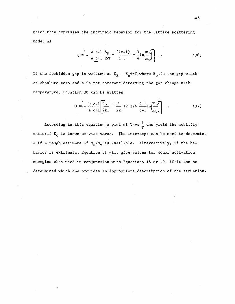
which then expresses thetntrinsic behavior for·the·lattice,scattering
model as
Q. - - (36)
,If the forbidden gap is written as Eg = E0 +aT.where E0 :is the·gap width
at .absolute zero and a is the .constant determing the ·gap change with
temperature, Equation -36 can be written
Q.= - .k.~~1~.Eo + ~ +2+3/4 c+lln(llln)\l e c+ 1 ~kT . .2k c-1 Inv~
(37)
According :to this equation a plot of Q-vs t·can yield the mobility
ratio if E0 .is known or-vice versa. '1:'he intercept can be used to determine
·aif a.rough estimate of ~/fflv·h available. Alternatively, if the he-
havior ·is extrinsic, Equation 3l :will give v;alue~ for ·donor activat"ion
:energies when used .in conj.unction ·with E:quatic;ms 18 or· 19, if it .can be
determined which one provides an appropriate·describption of the,situation.

CHAPTER IV
SAMPLES, APPARATUS AND EXPERIMENTAL TECllNIQUE
· Samples
Two: types of samples were used in this investigation, small rectan
gular rods of Sno2 grown· locally fr.om.a cu2o flux.and similarly-shaped
vapor grown samples*. The vapor;..phase samples were used mainl:y fo:i:-
optical .transmission· studies in the visible wavelength region •. As· mention
ed .previously the .rod~like crystals usually grow with. a sq1,1are. cros.s-sec
tional ax-ea· having from, 0.5 to one millimeter dimensions cm.a side, quite
adequate for measurements of the type performed.
The crystals taken. fr.0m the HCl bath .come in ,a .-variety of sizes.
There .. are very· large, poor. q1,1a,lity. crystal chunks: apparently wade up of
niany snialler· crystals that are· growing parallel .to .each other. These. are
f.ol!,nc;l to c_ontain niany inclusions of veins and bubbles. filled with. a· dark
red material. Crystals intermedj.atein,size between;thechunksand the
needlesare·the· ones chosen. for samples. 'l'hese.also have different appear
·ance_s. Some have very smooth glossy surfaces ,.and ethers: an "embossed"
surface pattern; some have veins: and bubbles .similar to those f,ouncf in the
.chunks and son1e. are essentially flaw free. · ·Freedom fr:om visible surface
and bulk flaws• provided the main criterion for choice. Due to the way the
crystals:are·grown.and cooled, m&ch cracking of long crystals eccurs·under.
*Grewn by· S.emi-Elements, Inc.,. Saxonburg, Pennsylvania.
46

47
the normal stresses impqsed by solidification of the melt, limiting the
length. Many times during the process of facing the crystal ends in
preparation for conductivity measurements, it was convenient to cut them
shorter·to elimix:iate small inclusions or surface flaws. The final length
of the sample crystals usually varied from one to five millimeters.
Two varieties of color are observed in the as~grown·crystals. They
appear clear. and transparent, some having a very faint. pink· t•inge . and
other~ not. The crystal color will be discussed in detail later. The
vapor grown· samples.are similar in size .and surface appearance but have
a deeper red color.
Sample preparation subsequent to recovery from the melt consisted.of
facing.the ends and cleaning. The facing proceedure involved securing the
crystal in the lapping·holder shown in Figure 9. This was done by heating
·0 the holder.and sample on.a hot plate to approximately 75 C.and melting
optical waxaround the crys:tal for reinforcement. After cooling, the
sample ends were abraded using 600A WETORDRY silicon-carbide paper on a
hard flat surface. The optical wax was then dissolved in.acetone using
.an· u!trasonic cleaning apparatus.* Much care in handling had to be exer.
·cised since chipping.and cracking of the crystals causes anomalous effects
·on electrical measurements.
Proper·cleaning of the !;!amples is imperative since the.as.;,grown
samples exhibit a very high resistance.and surface films could render the
electrical results erroneous. This was accomplished by four .. hour baths
in both hydr.ofluoric acid· and aqµa regia ( 7 5% HCl, 25% HN03). It was
la.ter found that the hydrofluoric acid bath .could be elimi~ated with no
*Ultrasonic work done on Gulton Inc;lustries Model GT.;.l:..10 Ultrasonic Cleaning Unit.

48
Copper Block Spring
Crystal
Figure 9. Holder for Lapping Ends of Samples.

49
adverse effects. The·bathswere followed by ultrasonic rinses in,acetone,
methanol and distilled water in that order. Particu_larcare bad to qe
taken to ins.ure that the acetone was completely removed after this portion
· of .the. cleaning procedure because it can leave. a film· on the ciystal sur-
face which when heated produces an etching effect. ! . -· • ; •
. No further preparatic.m was needed prior to experimentation. · The
electrical contacts, discussed 1ater, are p~atinum discs pressed to the
ends of the rectangular parallelapip-ed shaped crys~als.
Apparatus
The basic design· of the. sample holders for conductivity and thermo.
electric power measurements is very similar. The optical work on the
~eckman DK:.l and IR;..7 spectrophotometers used the sample holder provided
with the instrument.
Electrical Conductivity - Figure 10 shows .the hell jar apparatus construct-
· ed for conductivity measurements. The bell jar base was, cons.tructed to
have·three3/16-inch o.d., thermocouple pass;..throughs, two 1/4 inch solid
c:onductor pass.;.throughs and a 3/4 inch housekeeper coppe:r.;.to-glass seal
for .a vacuum port. It also provided support for the crystal holder system.
The diameter was 12 inc.hes. and supported a c.v .c. 10 o. d. x 14 inch bell
jar equipped with.a Neoprene gasket. All the feed throughs were soft
soldered to.the base.
The crystal holder fixture. and heater .. attached to the bell jar pase
.are. shown in Figures 11 and 12. Considerable care was- required to insure
a holder- de~;.ign· }:laving. a very high leakage;..resistance. and. also pr'oviding
very little· thermal co.nductiv.ity in order to prevent too, much heat leakage
from· the furnace. The arrangement also .allowed crystals .to be changed

Thermocouple Feed-Throughs
Conductivity Leads
Heater Lead
Bell
Vacuum Port
Figure 10. Bell Jar Apparatus for Conductivity Measurements.
so

Heater Current Lead Heater Fastener
Teflon
Quartz Discs
Conductivity Lead
Thermocouple Leads
I Lr-.'
I I
Base Plate
< >' Platinum Discs
~-~ .., I I
...... ~~Heater Pass-Throughs
Figure 11. Crystal Holder tor Conductivity Measurements.
Alumina Rods
Thermocouple Feed-Throughs
u, I-'

Tungsten Leads
Vacuum Port
Platinum Foil
Quartz Inner Tube
52
Quartz to Tungsten Seal
Quartz Envelope
Nichrome Windings
Figure 12. Quartz Furnace Design for Conductivity Measurements.

. 53
without dismant.ling the fixture. This was accom,pl;lshed by having a heater
that c.ould slide over the crystal. and be .positioned out. of the way. The
crystal is held between twol/4 inch o.d. alumi~a four-hole capillary rods.
One of these· is held stationary and spring tension· is applied ·to the bther.
Three leads pass through t~ capillaries .of each rod; two belong .to_ a
platinu,:n;..platinum (90%), rhodium. (10%) thermocouple. and the· thlrd is the
.conductivity current lead. The thermocouple is electrically insulated
from the current lead at the crystal by a quartz disc 1/4 inch in diameter
by 2 millimeters thick having .. a 1/2 millimeter· diameter hole dr,illed through
. it for the curren~ lead.* On,the end of the current lead in contact with
the .crystal is a platinum disc one millimeter thick by- 1/4 inch in diameter.
The heater construction is shown in Figure 12. Its laminated.design
consis.t.s of an· inner quartz tube 3/8 inch i.d. about which platinum -foil
0 .002 inches thick is wrapped. On top of this are wound two layers of
28, gauge Nichrome wire coated with asbestos shielding. The platinum is
used to stop hot spots from developing to cause uneven heating .of the
orysta_l. This portion of the heater is connected to. an outer ql;lart~ tube
having tungsten· .cur:t;"ent leads through it and a port for evac~ation. One
le13d is grounded to the platinum foil serving.as_ an electrostatic pickup
shield. The envelope .is sealed to. the inner portion· formi.ng. a vac1,1um
vessel. A rough pump vacuum is pulled on the furnace .and the capH.lary
sealed off reducing problems with .outgassing.
A portable vacuum· system-was constructed for use in conductivity
and thermoelectric power measurements. As seen· in:the schematj,c Figure 13,
it consists .of a Cenco Mechanical .Hyvac 7_ forepump and a c.v.c. Model GF.26
*Dr:i,.lled with Gulton Industries _Model D;..10 Ultrasonic ·DrHl. - . .

Edwards High Vacuum Lt-d.
OSlC Variable , ..... Ir
Molecular Sieve Veeco RG-75 Veeco DV-IM 1/:5 Trap Ionization Thermocouple
Gau~e Gauge
- Veeco Ionization and Thermocouple Gauge
Meter
c.v.c GF-26 Cenco Hyvac 7 Oil Fractionating Fore pump
Pump '-...
Figure 13. Portable Vacuum System Schematic Diagram.
v, .p.
5-5
glass oil fractionating pump. The pump is trapped using· Molecular Sieve
lfa5A in. an envelope .that can be contained in. a Dewar Flask for low temp
eratures when-needed. c.v.c. Octoil-S pump fluid is used and since it
is an ester, .no 9ack flow of pump oil should occur at room temperature
· when<the $ieve is properly· outgassed. The .accessories .as noted ,in the
· schematic :diagram. are thermocouple. and· ion, gaµge tubes. whi.ch. are Veeco rs
DV.;.lM. and R.G-.15· respectiv:ely. These. are controlled by a Veec:;.o RG-31A
combined. power supply. ·and- meters for both .. gauge tubes. An Edwar~s . High
Vacuum· Ltd._Model OSlC variable leak having.a 360° dial produces-a tairly
linear flow of 420 cc/min .per fuU. turn. of t.he dial up to 3000 cc/min
from,an atmespheric pressure source.and can be used .to vary .ambient
pressures. The- yacuum system was sealed directly to bothconduc.tivity
. and thermopower .. appa;r.atus to ,alleviate· preblems that might occur using
vacuum.grease.
Si·nce both the conducti.,vity and thermoelectric fixtures empleyed
two plati'num .. platinum (90%), rhodium ( 10%) the.rm.ocouples it was necessary
· to compare these ,to each other to ascertain· their reproducibility. Thh
.is especially important in the tempera.ture gradient determina.tion fqr
thermeelec:;.tric .power. The comparison, was. accomplished by using. a se.tup
as depicted in· Figure 14. Each thermocouple was- placed:in.a 1/4 inch
, alumina thermocouple tube that was fitted with,a quartz end .piece for
Junction p.rotection. This was cevered by a copper sleeve .and inserted
inte. a do:µble"".bq.re ·copper· cylinder. The. cylinder was 2 1/2 inches _in
·. dia:rneter_ and .l 1/'!, inches long with bores of 3/8 inches each extending
to.the center·of the copper block. The copper-block:and thermocouples
were pla:ced -into a muffle furnace capable of 950°c. Using. an ice bath
· reference -for·· both· thermoceuples and a Leeds. and :Northrup K-3 type

Alumina Tubing
Ice Bath
Ice Bath
Leeds and Northrup K-3 Type
Potentiometer
er Cylinder
I I J \ \ \
/ I
\
' Junction Protectors
Figure 14. Apparatus for Thermocouple Comparison. VI (1\

57
potentiome.ter fo'l; output detel;'mination it was found that the ceuples did
not deviate-more than 3 tenths of a ?egree centigx:ade frpm each ot;her tn
the .20. to 900°c · temperature range. The greatest difference occurred as
expected at the high temperatures.
Th,ermoelectric Power - The-thermoelectric power crystal holder and vacuum
enclosure can l:>e seen in F:Lgure 15. Once.again·thecrystal is supported
.between: two ,alumix:>,a capillary rods under spring tension. The origit;1al
design· consisted of two platinum heaters wound directly on the ends of
the .alumina rods. These could be controlled to give the des.ired temper-
. ature ·gradient. However, this configuration was. abandoned in, favor of
a simpler·systemof one quartz heater like that depicted in .Figure 12
that _c;.ould be positioned off;..center·to create the temperature gradient.
It was found that the open heaters evaporated platinum onto ·the .alumina·
.rods causing electrical leakage from heater to crystal and giving erro-
. neous results. · The two thermocouple junction leads are contained in
· the r.ods _and extended. out. of the system through hermetic pass throughs.
As before, the end contact is a platinum disc ;to v1hich the p~at,inum (90%),
rhodium (10%) lead is welded .to .form the couph. The platinum· wires are
· used for the thermoelectric .voltage determenati.on. A vacuum· seal between
crys;al holder.and enclosure ist!!,ade by means of an Q;..ring. The enclosure
.and. seat are water cooled with, a jacket .of copp:er 'tubing, soldered to the
cap..
Opt.teal Transmission ..: In· the optical work two ins.truments were used.
The .Beckman DK.;.l ·quartz prism recording· spectrophotometer covered the
185 to 3500m )lwlivelength range employing· hydr·ogen ( 18-,5;.;3}5:~. and tung ..
sten (3,5p~3500 ~ lamps. The long wavelengths were covered by a Beckman
IR;..7 spectrophotometer pr.ovided with. a Nernst glower as source for its

Vacuum Port
Copper Tubing Cooling Jacket
Heater Leads
Platinum Discs
Crystal
Thermocouple Feed-Throughs
0-Ring
Figure 15. Crystal Holder for Thermoelectric Power Measurements.
Heater Lead FeedThroughs
c::fq
v, OJ
59
2.5. to i5.4J.,( ratige. In both -cases the -crystals ·were -secured to a brass
plate by-means of optical wax. These plates had the appropriate hole
size drilled in them such that the maximum area of the-crystal was
exposed. The plates were placed :i,.n the·instrument crystal holder, In
the'IR-7, the-standard beam condenser was used to assure that .enough
-light -would be transmitted through the crystal for detection. When meas
uring :with double beam instruments such as these, one can·insert.a dia
phragm in the-reference beam cutting down its intensity to balance small
er signals. This type of diaphragm was used on both instruments since
the size of the·crystals were-such that only a fraction of the- instru-
ment beam could be transmitted.
Measuring Techniques
Two-probe te-chniques were used in the conductivity ·measurements.
This raises the·questi.on of contact problems due to.excessive-resistance
at the-crystal-metal interface. To-justify a two-probe method, four
probe measurements.were made along with V-I characteristic curves to
.check for rectification. Figure 16a shows the four-probe crystal holder.
Its basic design added to the,spring•loaded platinum-contacts two point
contact probes made of the Sylvania IN21 crimped tungsten :whiskers used
in point-contact transistor.s. The ·four-probe measuring. circuit· is sho_wn
in Figure·16b. Due to the-high-resistance of these.samples the normal
potentiometer circuit:could not be-used and Keithley Model 621 and610B
electrometers were·· employed instead.
A number of preliminary experiments were·performed with this basic
arrangement. The fircst compared.the effect of abraded and nonabraded con
tacts. If a battery and electrometer were ·connected in_,series-with the·two

Alumina Spacer
Crystal
luminum Block
- 84V.
-•
A
-----.,
Pressure Spring
Nylon Screw
latinum Discs
Kiethley Model 621
Electrometer
B
' c
Kiethley Model 610:B
Electrometer
D
..... -r -mr ,·-7.-'l I I \ I -- ~ ~-'.l.. _,_ .f-- -
-=.!- ~~-t,;£-\-1-H:-=.. L_ul,_ ,JL __
Spring
-
Figure 16. Crystal Holder for Measuring 4-Probe Conductivity.
60

61
point probes on the as-grown crystal surface, a very high.resistance was
noted. In·many cases it was greater than the·1014 o~s input resistance
of the electrometer. If, however, this experiment was performed using
:ah abraded area on the·surface under each·probe, the·resistance was
lqwered by many orde1:s of magnitude, .e.g., from·1014 ohn!.s to about·l08
.ohms. The roughened a:i;-eas were·prepared with the ultrasonic drill and
/fo600 .alumina grinding :compound. Th:1,s measurement·suggested that·either
the-as-grown ·surface causes. a very ·high contact resistance or there· i.s
an·insulating layer at the-crystal.surface.
A second configuration-similar to the-above·used the·current-path
from the broad abraded end contact of pressed platinum to,the point:cot1-
tact forboth·the abraded and nonabraded situatiotis. The broad platinum
end contact, of course, is never made to.a nonabraded crystal surface
since the end is faced to make this type of contact possible. Again two
·results were obtained. If the-point .contact was made·to-the as-gr~wn
.surface, avery·high.reststance .was measured.whereas on ·the·roughened
surface it· decreased many ordercs of magnitude. Along .. with these·· two ex
periments a third. was performed with point contact t.o one ·crystal. end and
broad pressed platinum to.the other end-which-sho,wed-that contact:size·did
not· influence the ··resistance. In .all experiments of· this type· the·,current
.was reversed to: see·· if any rectification •could be· noted. None .was.
It was-concluded. from these-trials that there·is a high resistance
layer at the as-grown-surface of the-crystal. Further ·substantiating evi.
dence of this is presented in the Results chapter. Similar conclusions .were
·reached by MacAvoy and Marley40 concerning their·vapor-grown-stannic oxide.
Conventional four-probe conductivity measurements were·made·usingthe
arrangement· in Figure ·-16a, b. In all cases the point contacts were made· to

62
abraded areas. This technique involved measuring in the dark -- four
voltages (A,ij,C,D),seen in the schematic diagram. By subtracting values
B·from A, C from B, and likewise D from C, the voltages dropped on three
sections of the crystal were determined. Similarly, data was taken.with
the battery reversed. In all but a few crystals examined, the.sectional
resistance ratios were comensurate .with the respective length ratios in
dicating homogeneous resistivity and the,sum of the,sectional.resistances
equalled the total end~to-end resistance. Situations where one large
sectional resistance occurred compared to the others could be·explained
by the presence of a mechanical flaw since if the crystal was reversed
in the holder-the·voltages were also reversed, ruling out excessive
contact resistance in favor of a resistivity inhomogeneity. Most·of the
four-probe measurements were ·made ·at· room temperature al though a·· few were
taken up to-150°C by placing the crystal holder on a hot plate and check-
ing .three or four intermediate equilibrium points.
Along with the four-probe experiments, V-I characteristics were·run
·in different-sections of the crystal to .check for rectification with
negative·results. A typical example is found in Figure 17. It must-be
pointed out however, that :care had to be takenin·placing the crystal in
the holder. When rectification was observed and no visible flaw devel
opments were apparent, it was due to placing the crystal at an angle in
the· holder causing uneven contact at the platinum di_scs. Remounting the
sample was found to remedy the Situation.
Reviewing these combined experiments, it·has.been·concluded that·the
· contact resistance is negligible, in ·.comparison to crystal resistance. and
that the resistivity. is homogeneous along the length of visibly sound
samples.

8
6
en l&J 4 a:: l&J a. :! ct
2 b I I- 0 z l&J a:: a:: ~-2 0
..J
~ en -4 ~ 0
-6
-8
SAMPLE . G - 23
-100 -50 0 50
CRYSTAL VOLTAGE - VOLTS
Figure 17. Typical Crystal Current as a Function of Voltage.
100
a, w

64
' A schematic -diagram of the• conductivity measuring system is shown in
Figure· 18. The circuit voltage was 2.1 volts and was prov.ided by one cell
of a 6 volt automobHe batter_y. Since data was taken point by point it
was necessary to. know when steady state :values of crystal current had been
reached. This was accomplished by .using. a Sargent. Model SR rec.order
driven by the Keithley 610B. When the data was recorded continuously be-
tween steady state points, it was found that the·crystal current varied
closely with crystal temperature on runs made in air at atmospheric pressure.
This temperature.was recorded by the sametype of recorder. The recorders
operate on,a potentiometric principle and allow the two thermocouples
built into the system -- one on. each side of the crystal -- to be connect-
· ed directly. By means of a switch either one could be hooked into the
recorder.and this fact was conveniently used to check when the furnace was
properly placed .so as to heat the crystal evenly.
Since the basic electrometer ac.ts as a .voltage sensing device, its
current ranges employ standard resistors over which voltages are.measured.
This being the case, when the electrometer scale is switched the voltage
.across the crystal changes such that the current read is not directly
proportional 'to the c:1;ystal conductivity. Therefore. a correction was made
to .the current so that a direct proportionality existed. This is best
explained by the following equations:
where Ia is the .actllal current through, the crystal and Vk- the voltage ·read··
across the standard resister Rk in the electrometer circuit. The current
desired. is that which would pass·through the·crystal if a constant voltage
were continuously applied. - ....Yb_ This would be Ic - Re where Re is the

65
~Electrostatic Shield , __ __/ __ --------, I I I I I I I I I I
Crystal
- r2.1 Volts
Kiethley Model 621
Electrometer
L __
Sargent Model SR Recorder
-
Ice Bath
PlatinumPlatinum(9 " Rhodium(l0%) Thermocouple
------
Sargent Model SR Recorder
Figure 18. Block Diagram of Conductivity Measuring'Circuit.
I I I I I I I I I I I
_J

66
crystal resistance and Vb the battery voltage. Therefore the correction
factor k is
because R = Vb-Vk c I
a and Vk = IaRk~'.. A computer program for the I.B.M. 1620
was used to. obtain values of constant voltage current versus measured current
from the above correction. The inputs to the program were battery voltage
and voltage range on the electrometer. All the conductivity data was cor-
rected in this manner.
A great deal of time was spent in obtaining a method of taking data
that would produce consistent.and reproducible results. It was found that
if a crystal was heated to a given temperature, conductivity as a function
of temperature was reproducible with increasing and decreasing points as
long as this temperature was not exceeded. The term llfixing" is used for
this procedure since it determines the conductivity versus temperature
curve. A rec.ord of each specimen's past thermal history was kept to observe
its ~ffect on subsequent data.
Vacuum measurements on conductivity were taken in the same way as
atmospheric pressure measurements except that the pressure·could be varied
fromio-5 torr to 10"" 1 torr by means of the variable leak. Corrections to
the data were the same as above.
The thermoelectric power data taken,was also dependent upon "fixing"
procedure. A schematic diagram of the measuring apparatus is shown in
Figure 19. Two platinum-platinum (90%), rhodium ( 10%). thermocouples were
in contact with the crystal. The platinum leads formed the thermoelectric
power or crystal voltage leads as well as one s.lde of the thermocouple
junction. A Keithley 610B electrometer measured .. the Seebeck voltage and a

67
~ Electrostatic Shield
,---- - - _/ _______ l
I I
Ice Bath
Sargent Model SR Recorder
Kiethley Electrometer Model 610B
Leeds and Nbrthrup K-3 Type
Potentiometer Ice Bath
I I I I I I I I I I I I I I
L_r-------------~ --i"
Figure 19. Block Diagram of Thermoelectric Power Measuring Circuit.

68
Leeds and Northrup K-3 type potentiometer measured the outputs fr.om the
two thermocouples. A Sargent Model SR recorder, provided with.a signal
from the electrometer, indica~ed when the crystal had reached equilibrium.
At each datum point the yoltage was read from the electrometer and I .
the electrometer then disconnected from the circuit. The K; .. 3 was then
connected and thermocouple voltages taken. This was done because the
input impedance of theK-3 was much lower than the·crystaL resistance.
The K-3 was then disconnected and electrometer once again inserted before
the temperature was changed toverify the first voltage reading.
Two types of data were taken. Thermoelectric voltage versus temper-
ature was measured in.air following a high temperature 11.fix" and at several
different ambient pressures varied with the vacuum system described pre ...
· viously. Data was taken point by point both with temperature increasing
and decreasing. While.at the high temperatures the gradient across the
crystal was reversed to see if a polarization effect could be noticed.
Measurements were taken on the way up and down without switching the grad-
ient to check reproducibility.
Much care had to be exercised in order to get good. results. High
resistance electrical leaks due to dirty pass.;.throughs and moisture occurr-
ed frequently. Each time the system was disassembled and cleaned. The
check for these leaks involved switching the heiater on and .off while
measuring with either the K-3 orelectrometer ah! watching for surges in
meter readings w.hich indicated their presence.
Because the single heater system was used to obtain the majority of
the reported data, gradients varied from s0 c at the lower temperatures
0 to about 30 c.at the high end of the measurement range. Preliminary
checks with the dual heater system indicated no significant dependence of
·thermoelectric power upon gradients of these magnitudes.

CHAPTER V
RESULTS
Introductory Remarks
This chapter ·presents the results of the experimentation described
in the previous chapter. It should be·noted that the measurements taken
on these single crystals under similar conditions are-found to be,quite
repeatable. Therefore the following data can be considered indicative ol
that gotten on a number of different crystals.
The ·results are broken·up into.three categories; electrical .conduc ..
tivity, optical absorption, and thermoelectric:;: power. The conductivity
data is concerned with measuremehts -made in·dry air ,and vacuum .along with
-related effects noted in· the ·process of taking data. Optical work pe,r~
formed.on the Beckman IR-7 and-DK-1 spectrophotometers as well as visual
observationis·included in the optical section. Measurements of thermo
electric po;wer-made in air and vacuum .are-p:i;-esented in the fini=il portion.
Conductivity Results - Atmospheric Pressure
As stated previously, the ·data presented is a .. consequence of a
technique required to give consistent results since·past thermalhistory
is vital in interpretation of .each graph •. · A. typical example is found in
Figure 20, of dark current (proportibnal to conductivity) 1versus·tempera
ture. '.fhis·depicts what occurs at·different "fixing" temperatures at
atmqspheric pressure. There are three thingsto note in this data. The
69

FIX TEMPERATURE - °C
I - 385 2 - 501 3 - 553 4- 627 5 - 781 6 - 950
PRESSURE - TORR
760
0
,cr10L.. ____ .i__• ____ ..1,._• ____ ..1,._1 ____ ~1-----..,__• ____ ~·-----L'----------......1 .6 1.0 1.4 1.8 2.2 2.6 3.0 3.4
70
Figure 20. Crystal Current as a Function of Reciprocal Temperature for Several 11Fixingn Temperatures.

71
first is the ·general increase in ,slope ·with. increasing. 11 fixin~.11 tempera
ture above·400°C~ Temperatures of 11 fixing 11 below this cause a decrease
in ·Slope. Also, the various·curves·have ·a tendency to focus at:a point
·which·is near·560°C. At.high. temperatures the-slopes of the.curves- are
reproducible and independent.of 11 fixing 11 temperatures.
A.two slope behavior·is-noted as the·result:of·fixing temperature
above·560°C. The-slope of this·curve·is reproducible following-a variety
of .past treatment. For example, a high temperature vacuum treatment:would
leave the room temperature conductivity in the·l0.;; 5 · (ohm:cm).; 1 range.
If then the,system were exposed to air at.atmospheric pressure and the
· crystal heated above 560°C, the high temperature portion. of Figure.20
would.be·repeated. It-seems that all treatments leave this piece of _data
unchanged unless the faces of the crystal become visibly etched. 'The
·various ways to,etch the.surfaces were·discussed previously.
When past-history is the controlling factor·in measurements, one·is
forced to look for consistencies and reproducibility. It was found that
for a given ."fixing" temperature the ·conductivity curve· is reproducible as
long,.as the crystal :i,s not heated above· the temperature of the fix. A
typical example of this reproducibilityis seen.in 'Figure 21, where-two
conductivity.ru~s were made; one·with-decreasing·temperature,.the·other
·increasing.· Near the 11 fixin~ 11 temperature· the crystal. current ·:was found /
to drift tJ · lower values when th;Ls temperature is exceeded.
Figure .22 shows thermally stimulated .currents ass.ociated with what
·_were calculated by Houstorl2 to. be additional current carriers excited from
a O .6 ev trapping·· level. This is the only_ piece· of data ._where a tempera-
ture rate was u.sed in. -experimentation. As ·can· be seen, the pe-ak decreases
with decreasing ··temperature rate· and also.moves to· lower temperature with

72
10·5
+ +
FIX TEMPERATURE - °C
\ 585 0
10·6 +\ o - INCREASING TEMPERATURE + - DECREASING TEMPERATURE
0
+\ +o
en \~ w a: ,0-1 w a.
,E
\ <(
I I-
\ z w a: a: ::::> \ (.)
...J ,o-a
<( \ I-en >-a: (.)
\ . ,o-9
10-,o a..---.11.........1.~--i.~ ........ ~...i..~ ...... ~....i...~-'---..i.;;.~..._--.i-.~,__--...... __, I.I 1.3 1.5 1.7 1.9 2.1 2.3 2.5
105/T - (°Kf I
Figure 21. Crystal Current Data Showing Reproducibility Below a Fixing Temperature.

I~~·,--,,-------------------------------------------.
u, lo"'II I.LI a: ~ 2 c I ... z I.LI a: a: ::::, 0
...J
~ u,
3 10·12
\\ 0 0
\ 0
\0
TEMPERATURE RATE
I - 167° C/MIN. 2- 90° C/ MIN. 3- 25° C/MIN.
1cr'a ______________ ..._ ________________________ __. ______ ~
73
~O ~2 2A 2~ 2.8 3.0 3.2 · 3.4
Figure 22. Thennally Stimulated Current as a Function of Reciprocal Temperature.

74
lower rates as found by Hou.ston. During.runs in conductivity it was found
that.at·low temperatures there were scattered points of data due to this
phenomena of photoconductivity. As it turned out although the crystal was
enclosed in a furnace there was enough light leakage to the crystal that
a light :shield had.to be used over the bell jar in order to remove·these
spurious effects. The data presented in this chapter·was taken with .care
that light did not reach the crystal. At·low temperatures (slightly above
room temperature) .a false level of conductivity can be obtained by this
process. Under certain conditions the decay of photoconductivity is very
slow so tJ1.at it is possible to ma.ke a complete run while· in the high
·conductivity state.
Vacuum Conductivity
The·effect of a common 11 fixing 11 temperature at·various pressures is
· exemplified in Figure 23. From atmospheric pressure to in the neighbor-
hood of·25 microns there is ltttle change·in the slope of the curves al-
though they are shifted to higher conductivities. However, suddenly the ••
·slopes shift to lower values exhibiting.a saturation in this temperature ,·
range. From this family of curves one can take the isoth~rms and produce
a plot as found in Figure 24, showing the short· range _in P,ressure in ,which
a significant change in c6nductivity is found. i
In the course of recording· the data .continuously for ,the point:":!:·bY"'
point plots, a slow conductivity change.with time at constant·temperature
.was noted in the range below 400°C. This was produced by changing·• the
heater voltage and recording the current as afunction of time oncethe
temperature stabilized. The direction of the change depended on the
direction of temperature chcilnge. In Figure is the temperature was increased

10- 6
PRESSURE - TORR I - 10-4
2- 6 X 10⁻⁴
3 - 2.5 X 10⁻²
4- 7.5 X 10⁻²
5 - 1.75 X 10⁻¹
6 - 6 X 10⁻¹
7- 760
FIX TEMPERATURE 830° c
0
i
--~~~~~~~ ..... ~~~--~~~--~~~_..~~~--~~~--. a .9 1.0 I.I 1.2 1.3 1.4
75
Figure 23. Crystal Current Versus Reciprocal Temperature for One Fixing Temperature at Various Pressures.

76
,o-'---------------------------------------------------------.
10"4
TEMPERATURE - °C I - 838 2 - 780 3 - 727 4 - 679
------lo
__________________ _J2~0
----------------_J3Lo
4 0
------------------------------'----------------------------_. ,o-4 10-3 10-2
PRESSURE - TORR
Figure 24. Crystal Current Isotherms Versus Pressure.

Cl) UJ a:: UJ Q..
:E <(
I t-16' z UJ a:: a:: :::> 0
..J
~ ~ a:: 0
.------, ---- 0 ----·-· -· -· 343 "C ;,,-- 0 0
~o ---:;8/~-·-·-·- -o-
/
-o-121 °C
"-----
10'9
ld'IO
-, I -II IO I I I I I I I I I I I I IO
0 5 10 15 20 25 30 35 40 45 50 55 TIME - MINUTES
Figure 25. Crystal Current as a Function of Time from Temperature Decrease
at 10-2 Torr.
60
-..J '1

78
whereas in Figure.26 it was decreased. At temperatures higher than 400°C
the conductivity and temperature stabilized together.
Figure.27 is an example of what happens to a 900°C atmospheric
pressure·fix upon taking data under vacuum conditions. The arrows indicate
·the temperature direction in which the data was taken. The ,sequence of
events was to take the crystal to 900°C in air, let it cool to room tenl-
perature,. pull a vacuum on it, and start taking data. with increasing
·temperature. At 424°C the· temperature was reduced and .data taken on· the
way down. It•is noticed that on return the level of conductivity·is shift-
ed .to higher values indicating more electrons in the conduction band.
In the vacuum ·work two factors are most important in the crystal
hhtory, the fixing temperature and fixing pressure. Very similar re-
sults are gotten when one is varied while the other is held constant and
vice versa. Qomparison of Figures 23 and 28 points out this fact. Again
the reproducibility of this data from treatment·to treatment.and crystal
to crystal is good.
40 Work done concurrently by MacAvoy and Marley .on the·vapor grown
Sno2 involved grinding 25 microns from the .width of the rectangular par-
allelepipeds and subsequent .equilibration. This was done in order-to get
a homogeneous resistance across thecrystal width since they noticed a
.resistance gradient into the cr~stal, the•resistance being highest at
the .,surface. Most• of the work done· in. our laboratory .was on as-grown
surfaces. As stated previously, the same high resistance surface noted
above is seen in the flux grown-samples. Using 600 grit WETORDY sil-
icon carbide paper the faces of a crystal were ground off and conductiv-
ity data taken. This is shown in Figure 29. Curvel shows the -starting
room·t~mperature·conducttvity prior to a run in air to 900°C. The return

10-5----
en l.&.I a:: l.&.I a.. I I ~ z ~- 10"6 0
----0---0 a:: ::, 0
...J <( ~ en ~ 0
____ 0 ____ 0 _ -o- o-
0 -0 o-
1so •c
10-7 '-~--'-----....1-~~'--~-i.~~..J-~....,ji;.._~-L.~~_,_~___.~~ ......... ~~~~~---i
0 5 10 15 20 25 30 35 40 45 50
TIME - MINUTES
Figure 26. Crystal Current as a Function of Time from Temperature Increase at 10-2 Torr.
.......
'°

,o-4 ·~ \_."' 0
\ 0
0
\ ,o-s U) la.I a:: 0 la.I D.. :& <( )/
I ..... z la.I 0 a:: a:: :) 0 0
....J
.! U)
10-& ~ ()
0
INITIAL FIX 900 °C 0
\ PRESSURE - TORR 1.5 X 10⁻²
0
\ 1Cf7
1.2 L4 1.6 1.8 2.0 2.2 2.4
1cf IT_ - (OK)-1 _
Figure 27. Crystal Current-Versus Reciprocal Temperature Showing Effect of Vacuum Fixing.
80
2.6

en LLI a:: L!J Q. :E <(
I I-z LLI a:: a:: :::> 0
....J
~ en >-a:: 0
81
10-2 FIX TEMPERATURE - °C
I - 209 2 - 289 '3 - 356
,o-a 4 - 540 0 PRESSURE - TORR o o\p
\o'\. \o 2.2 X 10⁻²
l<Y4 o~" ' 0 0\0~ -....:o
o ~-o \ -..0 o"' -o-0
10"!5 .\_ ·, -. 4
o ... 0 0\.
"' o'\ o'\ o 10-6 o "-o
"-o b"" '\o o 0 '\
10-7
\ 0
2'\ 0
0
10"'' \ 0
\ ,o-9 0
\0 0
1\
10-10
1.6 1.8 2.0 2.2 2.4 2.6 2.8 3.0 3.2 3.4
103/T - {°Kf I
Figure 28. Crystal Current Versus Reciprocal Temperature at One Pressure for Various Fixing Temperatures.

82
10-2 0
\\o oo\ PRESSURE - TORR
\\ 0\ I - 760 \o, o 2 - 760 oo 3 - 10- 3 \ 'o~
io-3 0 '
\ o~o 0 "o
\ ""' 0, 0
CJ) \ o'-..o IJJ 0
~ 0:: 10·4
\· IJJ 0 a. ~ < I \\ I- o, z IJJ 0:: 0:: 0 0 :J
~. 0 10-5 ....J
~ CJ)
~o >-0:: 0 -----0
0
IO~'-------L------..1-----__J,------.....1.-------1-..----_._----__, .8 1.2 1.6 2.0 2.4 2.8 3.2 3.4
Figure 29. Crystal Current Versus Reciprocal Temperature for Abraded Surface Crystal.

83
run to room temperatur~ is portrayed in Curve 2. Note the difference be-
tween Curve 2 and the high temperature fix curve of Figure 20. Normally
under these conditions of fixing, .the curve in Figure 20 would be·repro-
duced with th:i.s heat treatment but as can be .seen at comparable tempera-
tures, conductivities differ by orders of magnitude. ·upon heating in
one micron of pressure to.800°C the conductivity versus temperature is
seen in Curve 3. Note the difference between Curves 1 and 3 at room tern-
perature. D:i.scussions as to the reasons for this behavior will be delay-
ed until the next chapter.
Optical Absorption
A comparison is made between the optical transmission of Sno 2 in its
natural crystalline.state, cassiterite, and the flux-grown artificial
crystals in Figure·30. 31 This work was reported by Kunkle and Kohnke •
17 The transmission on cassiteriteis taken·from work done by Kohnke .• It
is believed that nature grows stannic oxide crystals by a hydrothermal pro-
cess which is responsible for the strong .absorption at 3.07.microns. It
is attributed to an 0-H stretching vibration as has been also reported by
Soffer50 on Ti0 2 and ~runner, Wondratschek and Laves 51 on qu,artz. This
absorption is not present, as would be expected, in the flux-grown samples.
The.short wavelength cutoff and long wavelength structure associated with
lattice vibrations, however, remains the same.
While involved with the different air and vacuum heat treatments,
measurements were made to ,see if these various processes·changed the vis-
·ible and infrared transmission ,spectra. Figure 31 shows the effects of
four different treatments. The order in which these.were gotten is as
follows:

z Q 1.0 ~ -:! fl) z er Ct= .... 0 UJ N ~ .5 <I: 2 3 z
0
.,,,,--/ \') I I/ I I
I I I I I I I ,,
I I I I I I I I
I I I I II I v I I
ii 2 3
GROWN CRYSTALS
--- NATURAL CRYSTALS
----,,,,,,~ --
4 5 6 7 8
WAVELENGTH (MICRONS)
9
Figure 30. Optical Transmission Comparison of Natural to Flux-Grown Sno2 Crystals.
10
<» ~

90...-------------------------------------------------------------
80 f<:.:..:..: ~
70
~ 60 u5 f/J
i ~ 50 Cl: a:: ~
~ 40
ti .J
~ 30
20
10
CRYSTAL HISTORY
I - NO TREATMENT 2 - 860 °C FIX AT 760 TORR 3 - 630 °C FIX AT 10-1 TORR 4 - 940 °C FIX AT 760 TORR
o------------_._ __________ _._ ........ _________ _._ ________ ___;.__. __________ __. 5 6 7
WAVELENGTH
8
MICRONS
9
Figure 31. Optical Transmission Showing Fixing Effect on 6 to 8 Micron Structure.
IO
00 v,

86
C::urve 1 - '.Caken on-an as-grown sample having·no :treatment·beyond facing _and cleaning.
Curve 2
Gurve·3
Curve'4
He_ated to 860,°C in dry -air and brought· back to ·room temperature.
-·3 Heated tos630°C in·lO torr of air and brought to
.-room temperature.
Heated.to 940°C·in dry air andbrought·to room·temperature.
No .attempt.was made in-the above·to.quench the crystals beyond let-
ting·them·cool with-the furnace. 'l'he·interesting point.·to 'note·is.that
there· is definitely a .reduction ... in the: transmission at 7 .5,}Afollowing high
-temperature-fixes-in air. The·total.spectrum.was run·from .wavelengths of
250 .millimicrons. to .. 9 ;5 .microns with the midrange ·showing: no :change.
Hqwever,-in·thevisible range there.were weak absorptions that·did not
significantly change with. treatment as shown in Figure,32. These small
a}?sorption,s might well have been missed or·ignored except for the·fact
·that :work done on :very ·red crystals obtained from Semi..:Elements, Inc.
sho.wed a·st.rong .absorption ·at 510 millimicrons (Figure·33) .and the-flux-
grqwn samples. sometimes exhibited -a faint pink ·hue. More ,will. be., said
about:crystal color below.
T_he as-grown ·samples directly from ,the .slug_ are .colorless and. trans-
parent. After -standing-in ·a vial for·extended lengths of. time (e.g., one
month) they take on a.pale pink tinge. '.['he·pale·pink can. be-bleached out
by thefollo.wing:treatments: 1) Heat.treatment'in·vacuum under one.torr
,with temperatures greater ·than, 500_°C ·but: not more· tl1an.·850°C · followed by
. slow coolins• ·care· h1:1.s · to .. be taken :with ·very ·lo.w pressures and high -teI!J.-
\
peratures because· this treatment· tends· to .etch.·the--surfa.ces of. the ,crystal.
-2) H:eat·treatment indry air to.very.-high temperatures, i.e., 85Q°C·or
greater, and a rapid quench tf room •temperatur~:~ The crystals following

8
7
6 z 0 in (I)
5 i (I) z ct ~ 4 1&J ~ ti 3 ..J 1&J 0::
2
350 400
WAVELENGTH 450
MILLIMICRONS
500
Figure 32. Optical Transmission Showing Visible Wavelength Absorptions.
87

100
90
80
.,. I 70 z 0 in ~ 60 :! Cl) z ~
~ 50
4.0
20
10
400 500 600 700 800
WAVELENGTH - MILLIMICRONS
Figure 33. Optical Transmission of Vapor-Grown Sno2 Crystal in the Visible Wavelength Range.
88

89
these treatments exhibited once again the colorless transparent char-
acter.
The pale pink tinge is produced in the following ways: 1) The
·crystal is exposed to light in air for extended periods of time at room
temperature •. 2) Heat.treatment in air to.temperatures above·500°C.and
slow cooling to room temperature. · :ay 11 slow11 , it· is meant .that· from 500°C
to.room temperature takes on the order of three·quarters of an hour.
The speed with which the crystal is cooled as well as the fixing
. temperature is a factor determinin&'ij,:l:pether the color appears or not. ·1<·''' fa:\'
This pink color is not seen in but only on reflected light.
A transitory yellow-green s observed when the crystal is
heated above 300°C.in air or·vacuum, however it again disappears upon
cooling •. As the temperature is increased the intensity of this color also
increases until the crystal takes on the reddish glow of black body radi-
ation. However, .when this experiment is performed in the dark no yellow-
green glow is seen. Only with reflected light is it·observed.
Thermoelectric Power Results
Due to the problems involved in. obtaining thermoelectric power ·re-
sults on·very high resistance samples the temperature range.was.limited
from 350°C to .850°C. Much care had.to be·exercised to assure that the
results were directly ~ttributable to the crystals and not to extraneous
effects. Figure 34 shows the results of thermoelectric po,wer versus tern-
perature as the temperature was increased and decreased respectively. For
this measurement the-sign of the voltage.was held the same on both runs.
However, at the high and low temperatures the sign was reversed to see if
any polarization effects could be noticed. None were. Subsequent data

TEMPERATURE - °C 400 500 600 700 800 900
-300....----------------..----------------.---------------.-------------,,-------------,,--~--------.--
0 0
' "' -500 ~ ...I 0 > O ·600 a:: 0 :'E
I -700 a:: w ~
~ -eool 2 a:: ~ 0 -900 w ...I w 0 ~ a:: -I w ::c ~
0
o~ o~
.~· 0----- 0 0
0
Figure 34. Thermoelectric Power Versus Temperature for a High Temperature Fix. '° 0

91
of a high temperature fi,x nature.showed remarkable reproducibility,-in the
high temperature ·region above the ·.thermoelectric power minimum. However,
the low temperature ·region .. showed much ·more. scatter of points,. although
the· trend was always the , same. In other words, the· shape of Figure,. 34
. was always· seen for ·high temperature· fixes ,with· the high temperature por
tion being ;most reproducible.
Using .a rule of thumb ·for ·thermoelectric power that.the higher·the
crystal resistance the higher the magnitude of thermoelectric power, it
·.would be expected that vacuum work should produce lo.wer values. This is
the case as presentedin Figure'3S. In this data the·two lqwer-valued
curves are gotten·from:runs taken at the.same·pressure but at two differ
ent·fixing·temperatures. For comparison·purpqses representative conduc-
tivity and thermoelectric power~are plotted together in Figure·36, as a
.. function of reciprocal temperature, since· calculations are ·made ·with this
type of data. It·· is to be· noted that· the thermoelectric power ·peaks in
·magnitude·in·the temperature range·in which the ·conductivity slopes break.

TEMPERATURE - °C
400 500 600 700 800 -300----------------,-------------------T'------------------,-----------------......... ----------------""1"""---------------------.
0 0 ..... en -500 ~ 0
~ a:: -6001 0 ~
I -700 a:: I.LI ;r: 0 Cl. -800
-uoo
0
0
PRESSURE - TORR
I - 760 2 - 2.0 X 10⁻²
3 - 2.0 X 10⁻²
O O~~~ 3 0
/ 0/0
-12nn----------------------------__;~--::;;;.....-------------------------------------------------------J
Figure 35. Thermoelectric Power Versus Temperature for Various Fixing Treatments. '° "'

\ 0
\ \ ~
\ -\
.\ 0
\ ;\ .""/. \
0
\ ,o ...
0
10-tl '----1---a.----L.___.____.___..,..._\~-__. .8 1.0 1.2 1.4 1.6 1.8 2.0 2.2 2.4 2.6
trf /T - (-Kf I
-400
-500
-600 0
-700
-800
0 ...... en ~ 0
~ 0:: 0 :i I
0:: -900 LLI
~ -1000 °
~ ...J
-1100 ~ 2 f5
-1200 ~
-1300
Figure 36. Comparison of Thermoelectric Power and Conductivity for a High Temperature Fix.
93

CHAPTER VI
DISCUSSION OF RESULTS
It is planned in this discussion ~o first introduce in a quali-
tative fashion a model explaining the general.behavior noted. With this r:
in mind, the data of the previous chapter ~ill then be discussed in rela-
tion to the model. Since the electrical properties of Sn02 crystals with
as-grown faces have been·found to be dependent on past pressure and tern-
perature·treatment even at relatively low temperatures (room temperature),
surface phenomena probably play a part in conductivity control. The
model which will be used for·explaining the behavior is based on the con-
ventional one-dimens:lonal flat-band energy scheme consisting·of donor
levels and at least one acceptor level. To be included in the consider-
ation is the surface double charge layer produced by immobile electrons
on the surface -- associated with chemisorbed oxygen\..- and a l;,alancing
distribution of positive ionized donor impurities in :the bulk. This sit-
uation in itself is not unusual and appears to be the· case for many n-type
semiconductors, although the depth of the space charge layer may vary
widely depending.upon bulk properties of the material. In fact often
this layer extends only a few hundred angstroms into .. the crystal. and can
be largely neglected as to effects on bulk electrical properties. For the
small expefimental specimens of Sn02, however, it·is believed that the
space charge layer· extends more deeply into. the crystal even producing·· in
certain cases a sample which is almost·totally 11 surface 11 • The space charge
layer thickness is defined as· the distance· from the surface to. the inter,ior
94

95
point where the electric field becomes zero. The·theory involved in this
type of one-dimensional band structure was presented in Chapter III.
Space charge·layers that extend deeply into the·bulk of the crystal
can be produced in sevE:ral ways. In essence -- inn-type semiconductors
with a negatively charged surface such a situation arises with a large
forbidde.rt gap and a very low donor density. The large gap assures almost
no ~lectronic transitions between valence band and conduction band with
only a few holes created in the valence band to migrate·under the influence
of the surface field and free surface~trapped electrons to drop the barrier
or to provide a. portion of the necessary balancing positive charge den
sity. An effective·low donor density can be accomplished in a couple of
different ways. The first that comes to mind is _the donor density that
is gotten with very pure materials. A second is one that does not neces
sarily involve pure materials but exists when there is abalance of bulk
donor densities and bulk acceptor densities. In this case donor compen
sation can occur by losing electrons from.the donor levels to the lower
lying acceptors completely immobilizing them at normal temperatures for
· thermal processes. A third situation that can occur is an. extension of
the other two and involves a donor density that is a function of the dis
tance into the crystal, having a higher density in the bulk. It·is reason
able then to suspect that electrons trapped at the surface would come from
donors lying close·to the surface but·since the·density there is small
the effect·is.spread further·into the crystal. An important.consequence
is that conductivity control by the,surface can take place when the number
of conduction band electrons and the number of surface traps or ·Surface
sites are comparable in magnitude.
The effect of such a space charge layer on the energy level.scheme

96
·in an n-type semiconductor is to bend the bands at the .surface to.higher
electron energies. This is understandable if on the surface there is a
high concentration of electrons. Then more-energy must be supplied to an
additional electron in the conduction band to.moveit·to the surface a-
gainst the repulsive force. Very little has been said to this point about
.the mechanism.for providing the negative ·surface charge.
The postulated model pertaining to flux-grown stannic oxide crystals
with as-grown faces consists of three or more donor-levels and at·least
one acceptor level with fairly high density. There is adsorption of
oxygen at the surface by electron -transfer (chemisorption) ,such that· the
space charge region extends into the·bulk of the crystal and the,surface
barrier to electron transfer is able to be raised or·lowered.by·heat and
pressure treatment. The donor densities are assumed to be functions of
the-distance into the crystal and to have a constant ionization energy as
measured from the bottom-of the conduction band.
It -has been observed for ZnO by Morrison and Miller~ 2, inferred for
53 NiO by Haber and Stone , and for numerous oxides-studied by Bevan,
Shelton and Anderson7 in the compressed powder form that oxygen adsorption
as a function of temperature reaches a maximum and then decreases with
increasing temperature above this point. Some authors ref er to 11 revers-
ible 11 and "irreversible" ranges of surface properties which seem to
f- 11 h' f d ' M . _--_ 54 th t . ' h o ow t 1.s pattern o a sorpt1.on. orr1.son states a one 1.s 1.n t e
region of_ irreversible adsorpt:'ion at· temperatures less than Tm as on the
sketch below and in the·reversible range above this-temperature. :Lt seems
reasonable to extrapolate this behavior to ,single crystal oxides. In
- fact,_ since it -is a practical impossibility to .measure adsorbed gas vol-
umes directly for small crystals,-it might be hoped that electrical

- 97
conductivity measurements could. provide a. sensitive· techr'lique -· for pro'."
viding this type of information.
t ·-Amt.
Oxygen Adsorbed
~m
Temperature ~
Turning now to-•the experimental results given in Chapter V, it
appea,r.s that·the behavior ·seen in the-lawertemperature·regiori of Figure
20 can be expl'ained by an oxygen adsorption mechanism.and its-effect:on
·the-space charge region. Note the general increase in -$.lopes with.in-
creasing. 11 fixing 11 temperature. The a,ssumed effect of the-fixing temper-
ature is to .determine the amount of oxygen chemically adsorbed at·the
-surface. It can.be calculated using an,ionic radius that.a monolayer of
oxygen.on·the·surface would produce on the order of 1015 electron:sites/
cm2 at the, surface. He>wever, in adsorption .work on ··variotJ.s. surf aces of
powders and pressed compacts, maximum number:s of oniy -1012-1013 oxygen
atoms/cm2 have been-observed .corresponding to 0.1'7" -to ,1% surface ·cove;t"
age. For ·'fixing-· temperatures below ~m the barrier· height_ is set. by a
given amount· of adsorbed oxygen and this· in turn indirectly ·dete.rmines
the -slope of the various electrical .conductivity_ curves· as found. in
Figure 20.
The mechanism visualized here is that at eachfixi~ temperature a
certain number of higher energy electrons in the,conduction·band can
,surmount· the surface barrier thus enabling them to .be· trapped by an oxy-
gen atom.which-is then-chemically adsorbed on the-surface. Successively

98
higher fixing temperatures thus produce higher surface barriers· since
more·. conduction electrons now have higher thermal energies allowing more
of them to reach-the-surface • .Simultaneously, however, ,what Morrisori54
terms "pinch-off" is occurring. - Initially ·the ·electron ·transfer rate to,
the-surface may be highbut ;;ts the,barrier·buildsit 11 pinch~s off 11 this
rate,-reducing it to.zero when there are no.,longer·free·electrons with
sufficient energy to get. over ·the- barrier. Subsequent .reduction ,of.· the
temperature.-will. leave·. the barrier· height at· its pinch-off value since
the·electrons bound on the.surface have no way of returning:to the bulk.
unless some additional desorption mechanism (e.g. photodesorption) ,is·
brought -into .. play. Temperatures above 'I'.m :provide ,an ,amount. of adsorbed.
oxygen characteristic of the·temperature, not because of a pinch-off
effect·but because in this temperature range·the.surface is apparently
in equilibrium with the ambient gas (reversibility) •. A con.sequence of'
this is that.on a conductivity run.where Uxing·is above T .and the-data . . . ,m . . ·~";
·. is taken as the temperature· decreases; pinch.:.off occurs at 'I'.m ,such that
·belo.w it the barrier is again·fixed by adsorption of the l'm amount. In
Figure 20 a general. increase in slope occurs with· fixes· bet:ween .400 _and
600°C. For· fix.es above· 600°C. the .slopes show only a .slight· increase al-
·though- the general level of .conductivity: may change.
The·equation governing. the lower-temperature,slope behavior·is Equc;1-
tion .22:which-gives the normal.free election density expression :when
·compensation is present. Two types of compensation-may be considered in
this case. First, that due to high -copper content in _subs ti tution-aL tin
·lattice-sites and secondly that due to-the-surface adsorption .acceptor
sites. The.bulk .compensation·has the·effect of completely deple.tingthe
~-····-/
'highest·lying donor levels of electrons as observed in recent photoelectric

99
55 measurements on·these·crystals • As higher·fixing·temperatures are-used,
lower donor levels become increasingly compensated.by the surface-states
and the conductivity_slopes show further·increase. A po,ssible,addition-
al reason for the increase· in ·slopes is· that the pre-exponential t.erm in
this equation may have an activated temperature dependence. This would
. lead.to a fixing temperature dependence-as well as the normal tempera-
ture relatio~ship. The effect then:would be to .add to the c1ctive normal
donor-level ionization energy the activation portion of the pre-exponen-
tial term giving _an .artifically large donor activation energy. Reasons
for such behavior are not :clear.a.syet, however.
Length The typical crystal dimensions were such.:that: the ·. . .. factor -was Area,
-1 -v30 .cm and in ·relation to the plot, 0- ==> I (crystal) ·1/AV where Vis
2 .1 vol ts. '[Jsing :a .free, electron density calculated from T at 450°C
and employing a-reasonable-value of.100.cm2/volt-sec·for·the mobility
·it can be seen·that to -completely·illll11obilize this number of free elec-
trans in:surface states associated with oxygen adsorption.would require
· · less than O .1'7o· of a mono layer of a9sorbed oxygen. This makes· plausible . . I
, signifi'cant .compertsation by surface .acceptors .. . . .
A possib~litywhich should also .be qonsj.dered,is that when adsorp-
·tion. occurs at .. the ·surface it ma;y cause· such-a high degree- of· compensa
tion· that _space charge region ·ext~rtcl1s effectively, throughout the ·crystal.
This of coU:1;s~ would lead. t~ a :fr0~'e''·electron density "'1hich·is, dependent· . ' '
'on ·t_he 'depth into.'the crystal and as the' bands are b(ant to. hig,her v'alues
a .smaller port'ion ~f the crystal ~ould be re'sponsible f'or the ,conduc
tion process. A naive way to e~~ress this is to say that the effective
cross sectio~al area.of the crystal is decreasing with higher fixing
temperatures. F,or progressively higher fixing ten\.peratures, this would

100
produce successively lower conductivities as is observed. It is not
obvious, however, why this should provide an,exponential temperature
dependence as is seen in the plots of Figure 20.
The reasons for the initial increase in,slopes for low fixing tern-
peratures (below 350°C) ,are not evident inlight of the above mechanisms.
59 Perhaps as suggested by Shear, Hilton and Bube in their work on CdS and
.c::;dSelayers, thermal desorption effects may outweigh adsorption processes
in this region of low conductivity.
The high temperature slopes from fixing temperatures above 560°G,
(if. calculated by Equation·· 14 assuming a lattice· scattering mobility
t . 1 T-3/ 2) . d' . f f- 1 2 7 propor 1ona to· · , are in 1cat1ve o an energy o ·- • ev. This
is tentatively identified as the intrinsic thermal gap energy with
j~stification to be provided later in this section. The reason that
intrinsic behavior might be seen at.high temperatures lies in the high
degree of compensation. The transition temperature from compensated-
donor and surface-controlled conduction,to primarily intrinsic behavior
· is at. the focal. point of· the various, law temperature curves. A slight
increase of conductivity level with increased fixing temperature is ob-
served in the,intrinsic range although this is not evident in terms of
the scale chosen·for Figure 0 20. This is presently attributed to an
annealing of the assumed inhomogeneous donor distribution near the sur-
face with consequent reduction of the·remaining,space charge layer thick-
ness and an increase of the effectiie cross sectional area for conduction.
The vacuum conductivity_ results shed mcfre · light on the above dis-
cussion. Figure.23 portrays theeffect of one fixing temperature at
· different pressures. It is noticed that as the pressure is decreased
from one'conductivity run to anotherthat the level of conductivity

.101
becomes higher as expected.if the decreased pressure.is responsible for
decreasing.the com:r1ensation due to:surface adsorptiotJ.. Hqwever,· in the
3 -2 ·.10- to 10 torr range· there is a sharp change o.f conductivity level
with pressure. 'l'his is best seen when plotting isotherms from Figure-23
on Figure,24. Once this sharp change has taken place-the conductivity
saturates which-is-taken tomean that the·electrons-in the conduction
band have originally come from donor· levels having ~mall. enough activa-
tion energies such that in this temperature range .. they are completely
ionized. Also .acceptor·levels at the-surface have apparentlybeen re-
moved so that this saturation remains. If all of the-electrons respon-
sible for conductivity-saturation-were contained in surface traps prior
to vacuum·heat·treatment then a calculation simil.ar,to that.described
above .would again show that. from O .1% to lt'o of a Jnonolayer of oxygen
coverage could provide all the necessary sites. A mobility had to be
assumed and the number employed in this-calculation was of the order of
100 cm2 /volt...-sec, a reasonable assumption· in· the· light, of work done by
Marley and Dockerty56 on vapor-grown Sn()z and on·cassiteriteby. Kohnke17 •
It is further interesting to note that·this saturation starts at the tern-
perature where the transition between·intrinsic and compensated conduc-
tivity·occurs on the atmospheric pressure data described above.
A further· implication obtained from Figure. 24 is. that .. th:i,.s is not a
.. donor defect .production mechanism as opposed to a desorption process
since at pressures below 10"'3 torr, the conduct:i,.v.ity a,gain becomes pres
sure independent. Defect production as noted bl7 R,udolplt 7 and Yahia58 is
·present at these temperatures on other-metal-excess oxides but would
continue to.increase until complete·reduction of the·crystal occurred
instead of leveling off.

102
Figures 25 and 26 might·be considered further substantiation of the
ad,sorption-desorption ·model. J:t is noted while taking :data .below 400_°C
.in vacuum·that a sle>w change of conductivity-with time occurs subsequent
.to a temperature change. This occu:i::s at·temperatures.at-whichdiffusion
of ions in and out of the lattice should be-extremely low. Figure .25 is
essentially saying that it takes on:the order of one·hour before 11 pinch
off11 ts completed causing the conductivity to,le;el off ·whereas Figure.26
.shows slow conductivity, rises associated with.desorptions. The·very
.·interesting·.· implication of these· results is that. the· adsorption ·versus
temperature curve described at the beginning of this chapter is not only
. ·reduced. in ·magnitude· but has it.s maximum -shifted to ·much·lower · tempera
tures ·when the ambient pressure is reduced below the·10- 2 torr range~
This obviotJ,sly warrants further ,study.
Eigure·34 shoMs·the·thermoelectric power. as afunction·of ·tempera-
ture. f'his. is the behavior noted with a high temperature· fix (intrinsic
. temperature·range) •. The-arrows indicate the direction in temperature in
, _.which ·the· data was taken. Note the·. difference· in ·the data petween · te~-, .. ·_.
perature on.the·rise and decrease-which is explained .as incomplete·high
t.emperat:ure ·fixing. Due · to . the fact· that the ·crystal was . taken . te> .. the
high temperature and quenched to <room·· temperature· before the· data .:.was
taken· the fix may not. have been :complete· since· the irreversibte, range·· in
ad,sorption .. was traversed too quickly. After·this'initial set\of measure-. .,"-,.,,
ment;s, the higher temperature portion of i:he·curve showed excellent:re-
producibility, both with temperatures increasing and decreasing. Thus
two ranges are seen in this data: 1) that on·thehigh temperature side
of the minimum corresponding to.the intrinsic range of behavior, and 2)
that on the low temperature side ·as indicative of compen,sa,ted donor

103
.behavior. In·the·range of·temperature studied the·thermoelectric power
·was alwiys negative.
Several times previously the· term. 11 inti.rinsic 11 has· been ·used to -de-
scribe the· highes·t temperature behavior of the specimens. Analysis, of
thermoele:ctric power data .will. be qsed to j'ustify this identifi~atio~.
One might:expect from the nature of the conductivity and.thermo-
electric power changes with temperature that the·highest temperature
,slope is indicative of electron :activation from a very deep..;lying.donor
.· level in the compensated material. Consid~ring Equations 22 and_.35 to
be pertinent the.slope of Q vs i.should provide a value for Ed as
should the ·slope of I. vs '¥" (assuming lattice-scattering mobility ·var
iation ·wfrh T,..;;3/ 2). However, these plo~s &ive ~d(Q) = L 15 ev and
.Ed(I) d(li35 ev,. a significant difference.
If it is assumed that the behavior is intrinsic and lattice scat-
tering.applies, then Equation 36 is pertinent and the thermoelectric . . pqwer·slope yields a value of 2~3 ev for the intrinsic gap.in·the·range
of me11surement. Here a value for· ~~i rvl has been· used .. to place a
lower limit on·the gap energy. A high mobility ratiq is consistent.with
results to.be presented shortly. 'l'he conductivity -slope, on·theother
·hand~ yields a.value of 2.7.ev for the·intrinsic gap at absolute.zero.
Using .a linear ·variation of forbidden gap ,with temperature, ' ... .
60 Eg: = E0 + aT .as suggested by Pearson and ~ardeen ·. , a value of
~4 . -3.5:xlO ev/~K is indicated for the coefficient,. a,by these two.pieces
· of data •.. This agrees very .well with ·values of ..;6:x:io-4 and -2:x:lo- 4
est':imated respectively by. Kohnke17 and Arai61 from optical adsorption
,shifts with temperature. The room temperature gap calculated in this
fashion is 2.59 ev, in excellent agreement with the indirect optical . 62
transition gap reported by Reddaway and Wright· •

104
16 61 Both Foex and Arai -have reported higher conductivity ·slopes
than .2.7.ev. on Sn02· However, these .wereoQservable in the same tem-
·perature range as i_s covered in t~e · present · data and ·were obtained using
powder or ·thin~'film:specimens. Results reported.here .would_suggest that
·these·higher slopes resulted from decreases of grain.boundary.or·inter-
particles resistances ~ssociated with,sintering:or agglomeration.
Returning to the ·intrinsic .calculation, a ratio. of ·mv > 100 .is esti-. . 1lln
mated. Although ·this justifies· the a~.sumption of a high mobility. ratio,
it.seems unreasonably-high. lt may ·be indicative of the restrictive
assumptions used in deriving thethe~oelectric power equations or·even
of the·· fact· that any space .. charge layer remaining :at high temperatures
would tend to.draw holes to the surface to desorb o~gen·and effectively
remove·them.from the conduction process. A point in favor of the·high
·ratio is that when· it is t.1,sed in ·combination .with a value of ·IDn = 0 .12m0
56 (as obtained by Marley and Dockerty on.·vapor-grown Sno2) to· calculate
an ·intrinsic electron .. density from Equation ·14, excellent agreement is
obtained with density-values calculated from the·conductivity data.
The,· low temperature portion of Figure ·34 .which is in the ·range of
compensation ·controlled c.onduction :Ls harder to explain. Loch19 notes
the same trend of behavior at these temperatures on ·.compressed po.wders
. of Sn02 although the ·mechanism may be vastly ·different.since his conduc- ·
tivity measurements in this temperature range show an essentially con-
·Stant value. Two :suggestions worthy cf further ·investigation are 1) the
introduction ofa new scattering ·mechanism .associated .with the pressure of
a· large ,space charge· region and 2) the possibility of p-type surface con
duction-in an. inversion·· layer which. is used by.Cimino, Molinari and Cramarqssa63
to:explain the p-type character of their Seebeck·voltage data.on .ZnO.

105
In Figure 35 thermoelectric power results from different fixing
prqdedures are shown. Note the general decrease in magnitude of the
thermoelectric power with increasing fixing·temperature·in vacuum. As
stated in the model presentation, the effect of these treatments is to
.introduce more electrons into the conduction band. Equation 35 shows
that if this is the case one would expect such behavior at.least in the
high temperature·· region where· this equation· is valid as .. long .as intrinsic
behavior is still partially masked by additional electrons released from
,surface acceptors under vacuum conditions. These fixing procedures then
.show results consistent with the same procedures in conductivity data
further -substantiating the model proposed.
Suggestions for Further Study
Further work in addition to the suggestions specifically made in
·the previous section is needed to ascertain more about the electrical
and optical properties of the flux-grown samples. The model in a very
real sense has been presented to provide a guide·to further study of
the surface effects, origins and densities of the donor and acceptor
imperfections, and the various optical effects.
To diversify the type of investigation that can be performed, a
continued effort must be expended in the area of Sno2 crystal growth
since the size of these crystals in many cases limits the types of
experimentation. Impurity control by doping is mandatory for elucida~
ting imperfection sources and for providing a better understanding of
thehost·lattice crystal fields. Two new possibilities for growth
warrant-special attention. One is growth using cuprous oxide flux, in
conjunction with a pulling process instead of the simple cooling process

106
used in this laboratory. The second is a modification of the zone re-
fining method where a solvent such as cuprous oxide is 11 drawn" through a
cylinder of Sn02 powder contained in a suitable crucible and furnace.
An appropriate design for ZnO gro!th has.recently been.reported by Wolff
and LaBelle64 •
It is found that when crystal surfaces are abraded, chipped or
cracked along· their total length, the·· room temperature conductivity in-
creases approximately five orders of magnitude. Figure 29.shows con-
ductivity measurements made on a crystal with the·surfaces abraded. In
·this case,subsequent·high temperature fixes in air decreased conduc-
tivity but not to the original value characteristic of crystals with ,_'1
as-grown·surfaces. A pressure dependence·of conductivity·is still
observed with abraded surface cryptals but it is reduced in scale.
These effects are very.striking and need to be integrated into the con-
duction.model. Field,Effect measurements and surface·potential studies
should give·insight·into carrier lifetimes at the surface and help de-
scribe creation and destruction of surface·states with temperature and
pressure treatments. Work should be done on both as-grown surfaces and
abraded surfaces.
Figure 31 depicts the long :wavelength structure in the optical
transmission data as changed by various heat treatments. The basic
structure is similar to that reported by Summit and Borrelli65 and
attributed by them to.combination vibrations of lattice fundamentals
found at longer wavelengths on Sn02 crystals. Itis felt that a know-
ledge of the,mechanism for the increase and decrease of the transmission
at 7~5.J-( would shed light·on the nature of the imperfections in the·crys
tal. Two possibilities to be investigated are.whether this added

107
absorption is due·to adsorbed oxygen and its weaker..;than-lattice bond
to·the crystal or to·lattice donor impurities that have migrated to the
surface cat1sing .a lattice distortioi;i in the.surface region.
The pinkhueand the effectiveness of various methods for producing
and bleaching it tnayalsobe associated with the lattice structure of
Figure 31. The absorptions in Figure 32, however,. show essentially no
change with·heat treatment·and may be·due·to ions or to oxygen:vacan-
cies in the lattice. It is intereSting:to note that the absorption in
Figure·· 32 just. below 500 millimicrons is of the proper wavelength to
.cause -- when the crystal is viewed under reflected light-- a pink color.
Suggestions have been advanced (e.g. by Morrison and Miller52 , Hauffe66
and others) that heat treatments of various kinds cause ion migration
. from bulk to .surface and vice versa. While near the.surface the ion
concentra.tioh may be great• enough to provide perceptible color. A study
of this behavior under different heat treatments coupled with diffusion
work using tiri and/or copper might aid in identifying these absorptions.
As mentioned earlier., a transient· yellow-green color appears when
the crystal are heated above 300°C in room light although this has not
been visually observed in the dark. Consideration has been given to
trying .a glow curve analysis which could shed light on the energy values
of the impurity levels and corroborate photoelectronic data. This,
however, is an experiment in which the crystal size is a distinct·hin-
drance,. since radiation detection would be very difficult with small
specimens.
Conductivity measurements must be extended to higher temperatures
and lower-pressures to verify the distinction between intrinsic and ex-
trinsic·effects. These measurements should also identify·the temperature

range in.which .defect production begins to play a significant role in
the conductionmechani,sm.
108

.1.
2.
3.
4.
5.
6.
7.
8.
lQ.
11.
12.
13.
14.
15.
16.
17.
18.
BIBLIOGRAPHY
Verwey, E. ~· w., SemiconductingMaterials, ed. H.K. Heriisch, Butterworths Scientific Publications Ltd., London (1951).
Gray, T. J., Semiconducting Materials, ed. H.K. Henisch, Bul;;ter¥1orths Scientific ·Publications L.td., London (1951).
Gray, T. J., Chemistry of the Solid State, ed. w. E. Garner Butterworths Scientific· P4blications Ltd., London ( 1951).
Grant, F. A., Rev. Mod. Phys., 31, 646 (1959).
Heiland, G., Mollwo, E. and Stockman1=1, F., Paper in S9lid. State ·Physics vol 8, Acedemic Press, New York, (1959.).
Zhuravlev, V.-A. and Kulitskii, v. N., Kinetics and Catalysis,~' 90 (,1963).
. ..... Bevan, D. J. M., Shelton, :f • . P. and Anderson, J. s., J. Chem. Soc.,
London, 1729 · ( 1948).
Arghiropoulos, B. M. and Teichner, S. J., J. Calalysis l, 477 (1964).
Wyckoff, R. W. G., Crystal Structur.es, .John Wiley.and Sons (1963).
Bauer, .G. , Ann. Physik 30, 433 ( 193 7).
Fisher, A., z .• Naturforsch, 9a, 508. ( 1954).
Ishiguro, K., et aL, J. Phys. Soc. Japan, 13, 296 (1958).
Le Blanc, M. and Sache, H., z. Bhys.ik, 32, .887 (1931).
Guillery, P., Ann. Physik, 14, 216 (1932).
Miloslavskii, V. K. and Lyaskenko, S. P., Optics and Spectrosc., t,r., ]...., 154 (1959).
Foex, M. , Bul 1. Soc. Chem. , France, _!l, 6 · (1944).
Kohnke, E. E., J. Phys. Chem. Solids, 23 ~ 1557 (1962).
Hurt, J.E. and Kohnke, E. E., Relation Between·Photoconductivity ·· a·nd Chemis.orption Kinetics' ·for· S·t-atrrri:'c ''.ex-;i::d-e···erystals. Tech. Report 4F2, May 1962 - Jan. 1963, Contract /FNonr.;..2595(01) •
. 109
llO
19. Loch, L. D., J. Electrochem. Soc., 110, 1081 (1963).
20. Reed, T. B., Ro.ddy, J. T. and Mariano, A. N., J. Appl. Phys·., 33, 1014 (.1962.).
21. Marley, J.· A. and MacAvoy, T. c., J. Appl. Phys., 32, 2,504 (1961).
22. Houston, J. E., Pho.toelectronic Analysis of Imperfections in Grc::,wn . Stannic O:x:ide Crystals. Tech. Report #4, Feb. 1965, Contract IFNonr ~ .. 2595( 01). ·
23. Scharowsky, El, z. Physik fil, 318 (1953).
24. · Nielson, .J. w. and Dear.born, E. F., J. Phys. Chem., 64, 1762 (1960). ,.
25. Laudise, R. A., I<olb, E. D. and Caporaso, A •. J., J. Am. Ceramic. Soc • . 47, 9 (1964).
26 •. Moore Jr., C.H., Mining Trans., 184, 194 (1949).
27. Verneuil,. A. V. L., Proce·ss of Pro~uci,g Synthetic Sapphires, u. s; Pat. 1,004,50,?, Sept. 26; 1911.
28. White, E. A. D. ! Nature, London, 191, g61 (1961).
29. Nielson, J. W. and DeaJ;'.born, E. F.; J. ·l!>hys. Chem. Solids, .!, 202 '(1958).
30. Laudise, R. A. and Ballman, A.·A., J. Am. Chem •. Soc.; 80, 265,?(1958) •
. 31. Kunkle, H. F. and Kohnke, E. E., J. Appl. Phys., 3.6, 1489 (1965), . -.-
.32. Harvill, M. L. and Roy, R., Am. Ceramic Soc. Bull., 44, 297 (1965).
33. ylalker, A. C. and Buehler, E., Bell Laboratories Record, Jan·. (1959).
34. Reed~ ·r. B., Private Communication.
35. Kunkle, H.F., Unpublished Master•s·Report, Oklahoma State University' (1961).
36. Urazov, _G. G., Speransbaya, E. I. ,J. Inorg. Chem., USSR, _!, 1413 ( l956).
37. ~arezal.<., v. J •. and Insley, R •. H., J. AI)i. Ceramic S.oc. Disc.- and ·· .Notes, 45, 144 ( 1962).
38. Mellor, J. W., Mellor•s Modern Inorganic Chemistry, Lonijman Press (19.56).
· 39. .Greninger, A •. B., Trans. Am. Inst. Mining· Met. Engrs. 117, 61 ( 1935).

·. 40.
41.
42.
43.
44.
'45.
·46.
47.
48.
' -49.
50.
51.
· 52.
53.
54.
55.
56.
57.
58.
59.
. 60.
61.
lll
Marley, J. A. and MacAve;>y, T. C. , · lnvestigati,ons of the ~echanj.sm of. Single .Qrystal Growth in High Tem.perature Sys~em. F:i.nal
· Report, June 1961 - June 1962, Contract No. AF 19(604).;.8447.
Swanson, H. E. and Tatge, E~, Nat 1 1.Bur. Standards (U.S.), Circ. 539, l, (1953).
Blakemore, J. S., Semiconductor Statistics, Pergamon Pres1;1, New York, (1962).
Smith, R.·A., Semiconductor-s, Cambridge Press,'(1959).
Garrett, C. G. B., and ijrattain, W. H., Phys. Rev., 99, 376, (1955).
Kingston, R.H. and Neustadter, S. F., J. Appl. Phys., 26, 718 (1955).
Dousmanis, G. C. and Duncan, R. C., J. Appl. Phys., 29 1627 · (1958).
Young, C. E., J. Appl. Phys., 32, 329, (1961).
Seiwatz, Ro: and Green, M., J. Appl. Phys., 29, 1034 (1958).
Johnson, v. A., Article in Gibson, A. F., Progress in Semiconductors, John Wiley and S.ons, New York, (1956).
Soffer; B. H., J. Chem. Phys., 35, 940 (1961).
Brunner, G.: Wondratschek, H. and Laves, F., Natu:n1:i,.,ssenschaften, 46, 664 (1959). .
Morrison, s. R. and Miller, P. H., Jr., J. Chem. Phys., 25, 1064 (1956).
Haber, J. and Stone, F'. S., Proc. Chem. Soc, 424 (1961).
Morrison, R., Article· in Advances in Catalysis,. Acedemic Press, New York, (1955).~
Houston,· J. E. and Kohnke, E. E., J. Appl. Phys.,· In Press.
Marley, J. A. and Do_ckertr, R. C., Phys. Rev., 140, 304 (1965),
Rudolph, J., z. Naturfor:sch, 14a, 7,27 (1959).
Yahia,·J., Phys. Rev.,:130, 1711, (1963).
Shear,·H.,·f!ilton, E. A. and Bube, R. }J.., J·. ·Elect::rochem. Soc., 112, 997. (1965) •.
Pearson, G, L. and Bardeen, J., Phys. Rev., 75, 865 (1949) • ' . -
Arai, T., J. Phys. ·soc. Japan, 15, 916 (1960). .. ' .. - .

112
62. Reddaway, S. F. and Wright, D. A., Brit. J. Appl. Phys.,~' 195 (1965).
63. Cimino, A., Molinari, E. and Cramarossa, F. J.,Gatalysis, l, 315 (1963).
64. Wolff, G .• A. and LaBelle, H. E., Jr., J. Am. Cer. Soc., 48, 441 (1965).
65. Summitt, R. and Borrelli, N. F., J. Phys. Chem. Solids, 26, (1965).
66. Hauffe,·K, Article in Advances in Catalysis, Acedemic Press, New York, (1955).

APPENDIX
MON$$ JOB 223340009 MON$$ ASGNMGO,A2 MON$$ . ASGN. MJB ,A3 MON$$ MODE GO, TEST MON$$ EXEC FORTRAN,,,,,, ,XRAYPRO
DIMENSIONITS( 101) ,RECHTS( 101) ,XLINKS( 101) ,A(30 ,30) COMMONA,J
00002 FORMAT(l4 ,2X,F7. 5, 2X,F6r4·, 2X, 12, 2X,I2, 2X, 14) 00003' FORMAT( lHl, 2x:, 7HFlLM=E- ,I4; 6~C,.6HDATE= , 12, lH/, 12, lH/, 14, 6x,
Cl1HWAVELENGTH=,Fff.5·,4X,28HSHRINKAGE COR . 00004 FORMAT(F5.3,1X,F5.3,1X,I2) 00009 FORMAT(2X,25HCENTER FRONT REFLECTIONS=,i9·. 5 ,/) 00018-FORMAT(2X,4HLINE,6X,4HLEFT,6X,5HRIGHT,41,14HTHETAS(COR)
C41HSINES SINSQR INTENSITIES D-V 00020 FORMAT(2X,I2,5X,F8.3,2X,F8.3,4X,F8.4,3X,F9.6,1X,F9.6,6X,I3,
G6X F8.5) ' .. .
00012 READ(l,, 2 )IF1LM ,RAD, CORF AC ,MONTH, IDAY, IYEAR 00050 IF(;'!'.{(fLM.EQ.O)STOP ' 00057 WRITE(3,3)IFILM,MONTH,IDAY,IYEAR,RAD,CORFAC
CENTER=O.O TAB=O.O J=l
00005 READ(1,4)XLINKS(J) ,R-ECHTS(J), ITS(J) IF(XLINKS(J) .EQ.O.O)GOT032 IF(RECHTS(J) .EQ.O.O)GOT039
. 0000 7 CENTER=CENTER+(RECHTS (J )+XL INKS (J)) / 2. 0 . · TAB=:TAB+ 1. 0
GOT039 00032 IF(RECHTS(J) .EQ,0,.0)GOT08 .00039 }=J+l .
GOTOS 00008 GENCEN=CENTER/TAB
WRITE(3 ;9 )GENCEN WRITE(3, 18) JJ=J;..l D022M=l,JJ IF{XLINKS(M) .NE .O.O)GOT013
. DEGREE~5. O*((RECHTS(M)-GENCEN)*CORFAG) · GOT017 '
. 00013. IF(RECHTS<(M) .NE. O. O)GOT015 DEGREE=5.0*(GENCEN:.XLINKS(M))*CORFAC GOT017
00015 DEGREE=2.5*(RECHTS(M)-XLINKS(M) )*CORFAC 00017 THETA,,;;,DEGREE*0.01745329 (Omit for Back Reflectian) 00017 THETA=l.570795-DEGREE*.01745329 · (Om.it for Frant Reflection)
113

SN=SIN(THETA) . A(M, l)=SN*SN
. DAV=RADI (2.0*SN) ·:o0022'WRITE{3 ,2CJ)M,XLINKS(M) ,RECHTS(M) ,DEGREE,SN ,A(M, 1) ,!TS:(M),DAV
. IF(J .LT .31)CALLMATRIX . . .
GOT012 ENO
MON$$ EXEQ FORTRAN: SUBR:OUTINEMATRIX . DlMENSIONITS(lOl),RECHTS( 101) ,XLIN&S( H>l) ,!(30 ,30) COMMONA,J .
. 00030 FORMl\.'l'( IX, 12, 15(F8 .!l)) --crOCJJ'5 FORMAT(-2X,.I2, 15(:FS. 5))
114
00040 FORMA;T0Hl ,4'4H . TABLE OF DIFFERENCES FOR SIN SQUARED THETA, ,I/I) 00045. FORMAT(1Hl,23H DIFFERENCES CONTINUED,//) .
WRITE(3,40) JJ==J-1 D01011=2 JJ
. ' ' ' .DC>lOOK=;r ,JJ A(K; I)=A(K, 1)-A(L-l:, 1)
00100, C:ONT·INUE . ,.
:001ot CONTINUE · . DOllOL=l·;l5
0.0110 .WRTFE'(3,.,J.O )L, (A(L,N),N=l ;L) IF'(J-.LE·. t5)RETURN -. D0120L=l6,J
. :00120- WRITE(3 ,:lO)L, (A(L,NJ:,N=L 1.5) WRITE(3,45) . .
. D0130L=l6 ,J 00130 WRITE:('3 ,35)1, (A(L,N) ,N=16 ;L)
RETURN . .
· END MON$$
· MON$$-
EXEQ LINKLOAD PHASE 'RAYX CALL XRAYPRO ElXEQ RAYX,MJB
VITA
Howard Franklin Kunkle Jr.
Candidate for·the Degree of
Doctor of Philosophy
Thesis: HIGH TEMPERATURE CONDUCTIVITY OF GROWN STANNIC OXIDE SINGLE CRYSTALS
Major F,ield: Physics
Biographical:
Personal Data: Born.at Pittsburgh, Pennsylvania, March 9, 1937, the son of Edna and Howard Kunkle.
Education: Attended elementary school in Belleview andMcMurray, Pennsy1yania;c graduated from Peters Township High School,
· McMurray, Pennsyl~ania, in 1955; received. the Bachelor of Arts degree from Washington and Jefferson College, Washington, Pennsylvania, with a major in Physics, in June, 1959; re·ceived the Masters of Science.degree from Oklahoma State · University; with a major in Physics, in August, 1961.
Professional Experience: After receiving the M:aster of Science ,degree, worked the summer of 1962 with Westinghouse; Astronuclear Laboratory, Pittsburgh,Pennsylvania.