Embed Size (px)
Citation preview

May 2017 DocID11640 Rev 2 1/13
This is information on a product in full production. www.st.com
STPS30170C
High voltage power Schottky rectifier
Datasheet - production data
Features High junction temperature capability
Good trade off between leakage current and forward voltage drop
Low leakage current
Avalanche capability specified
ECOPACK®2 compliant component for D²PAK on demand
Description Dual center tap Schottky rectifier designed for high frequency switch mode power supply.
Table 1: Device summary
Symbol Value
IF(AV) 2 x 15 A
VRRM 170 V
Tj (max) 175 °C
VF (typ) 0.69 V
K K
A1 A1A2 A2
D2PAK
A1K
A2
TO-247A1
KA2

Characteristics STPS30170C
2/13 DocID11640 Rev 2
1 Characteristics Table 2: Absolute ratings (limiting values, per diode, at 25 °C, unless otherwise specified)
Symbol Parameter Value Unit
VRRM Repetitive peak reverse voltage 170 V
IF(RMS) Forward rms current 30 A
IF(AV) Average forward current
δ = 0.5, square wave TC = 150 °C
Per diode 15 A
Per device 30
IFSM Surge non repetitive
forward current tp = 10 ms sinusoidal 220 A
PARM Repetitive peak
avalanche power tp = 10 µs, Tj = 125 °C 750 W
Tstg Storage temperature range -65 to +175 °C
Tj Maximum operating junction temperature (1) +175 °C
Notes:
(1)(dPtot/dTj) < (1/Rth(j-a)) condition to avoid thermal runaway for a diode on its own heatsink.
Table 3: Thermal parameter
Symbol Parameter Max. value Unit
Rth(j-c) Junction to case
D2PAK Per diode
1.6
°C/W TO-247 1.5
D2PAK Total
0.95
TO-247 0.9
Rth(c) Coupling D2PAK
Coupling 0.3 °C/W TO-247
When the diodes 1 and 2 are used simultaneously:
ΔTj (diode1) = P(diode1) x Rth(j-c) (per diode) + P(diode2) x Rth(c)

STPS30170C Characteristics
DocID11640 Rev 2 3/13
Table 4: Static electrical characteristics (per diode)
Symbol Parameter Test conditions Min. Typ. Max. Unit
IR(1) Reverse leakage current Tj = 25 °C
VR = VRRM -
20 µA
Tj = 125 °C - 5 20 mA
VF(2) Forward voltage drop
Tj = 25 °C IF = 15 A
-
0.92
V Tj = 125 °C - 0.69 0.75
Tj = 25 °C IF = 30 A
-
1
Tj = 125 °C - 0.8 0.86
Notes:
(1)Pulse test: tp = 5 ms, δ < 2% (2)Pulse test: tp = 380 µs, δ < 2%
To evaluate the conduction losses use the following equation:
P = 0.64 x IF(AV) + 0.0073 IF2(RMS)

Characteristics STPS30170C
4/13 DocID11640 Rev 2
1.1 Characteristics (curves)
Figure 1: Average forward power dissipation versus average forward current (per diode)
Figure 2: Average forward current versus ambient temperature (δ = 0.5, per diode)
Figure 3: Normalized avalanche power derating versus pulse duration (Tj = 125 °C)
Figure 4: Relative variation of thermal impedance junction to case versus pulse duration (D²PAK and
TO-247)
Figure 5: Reverse leakage current versus reverse voltage applied (typical values, per diode)
Figure 6: Junction capacitance versus reverse voltage applied (typical values, per diode)
0
2
4
6
8
10
12
14
0 1 2 3 4 5 6 7 8 9 10 11 12 13 14 15 16 17 18
PF(AV)(W)
=0.05
=0.1 =0.2 =0.5 =1
T
=t /Tp tpIF(AV) (A)
0
2
4
6
8
10
12
14
16
18
0 25 50 75 100 125 150 175
IF(AV)(A)
Rth(j-a)=15 °C/W
T
=t /Tp tp Tamb(°C)
P (tp)
P (10 µs)ARM
ARM
0.001
0.01
0.1
1
1 10 100 1000
t (µs)p
0.0
0.1
0.2
0.3
0.4
0.5
0.6
0.7
0.8
0.9
1.0
1.E-03 1.E-02 1.E-0
Zth(j-c) /Rth(j-c)
=0.1
=0.2
=0.5
Single pulse
T
=t /Tp tptP(s)
1.E+00
1.E-01
1.E+00
1.E+01
1.E+02
1.E+03
1.E+04
1.E+05
1.E+06
0 10 20 30 40 50 60 70 80 90 100 110 120 130 140 150 160 170
IR(µA)
Tj=150°C
Tj=125°C
Tj=25°C
Tj=75°C
Tj=175°C
VR(V) 10
100
1000
001001011 0
C(pF)
F=1MHzV
OSC=30mV
RMS
Tj=25°C
VR(V)

STPS30170C Characteristics
DocID11640 Rev 2 5/13
0
10
20
30
40
50
60
70
80
0 5 10 15 20 25 30 35 40
SCu(cm²)
Rth(j-a) (°C/W)
Epoxy printed board FR4, eCU= 35 µm
Figure 7: Forward voltage drop versus forward current (per diode, low level)
Figure 8: Forward voltage drop versus forward current (per diode, high level)
Figure 9: Thermal resistance junction to ambient versus copper surface under tab for D²PAK (typical values)
IF (A)
0.0
2.5
5.0
7.5
10.0
12.5
15.0
0.0 0.1 0.2 0.3 0.4 0.5 0.6 0.7 0.8 0.9 1.0
Tj=25°C
(Maximum values)
Tj=125°C
(Maximum values)
Tj=125°C
(Maximum values)
Tj=125°C
(Typical values)
Tj=125°C
(Typical values)
VF (V)
IF (A)
1
10
100
0.0 0.2 0.4 0.6 0.8 1.0 1.2 1.4 1.6
Tj=25°C
(Maximum values)
Tj=125°C
(Maximum values)
Tj=125°C
(Maximum values)
Tj=125°C(Typical values)
Tj=125°C(Typical values)
VF (V)
Package information STPS30170C
6/13 DocID11640 Rev 2
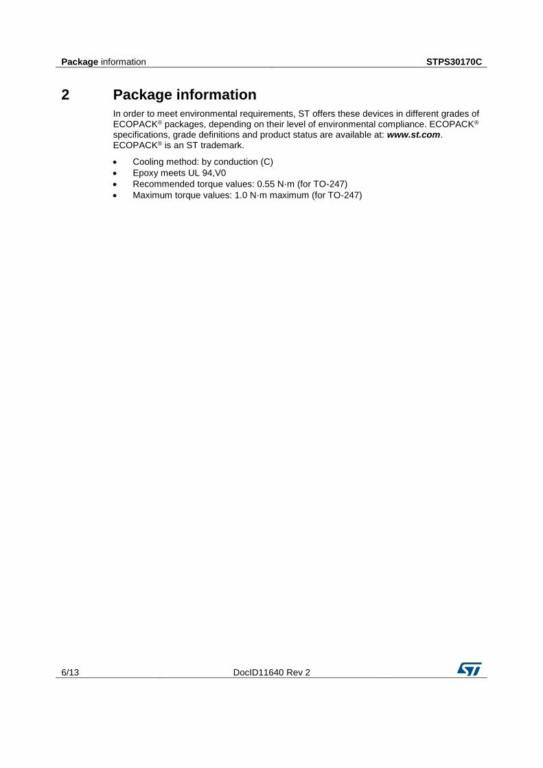
2 Package information
In order to meet environmental requirements, ST offers these devices in different grades of ECOPACK® packages, depending on their level of environmental compliance. ECOPACK® specifications, grade definitions and product status are available at: www.st.com. ECOPACK® is an ST trademark.
Cooling method: by conduction (C)
Epoxy meets UL 94,V0
Recommended torque values: 0.55 N·m (for TO-247)
Maximum torque values: 1.0 N·m maximum (for TO-247)

STPS30170C Package information
DocID11640 Rev 2 7/13
2.1 D²PAK package information
Figure 10: D²PAK package outline
This package drawing may slightly differ from the physical package. However, all the specified dimensions are guaranteed.
Package information STPS30170C
8/13 DocID11640 Rev 2
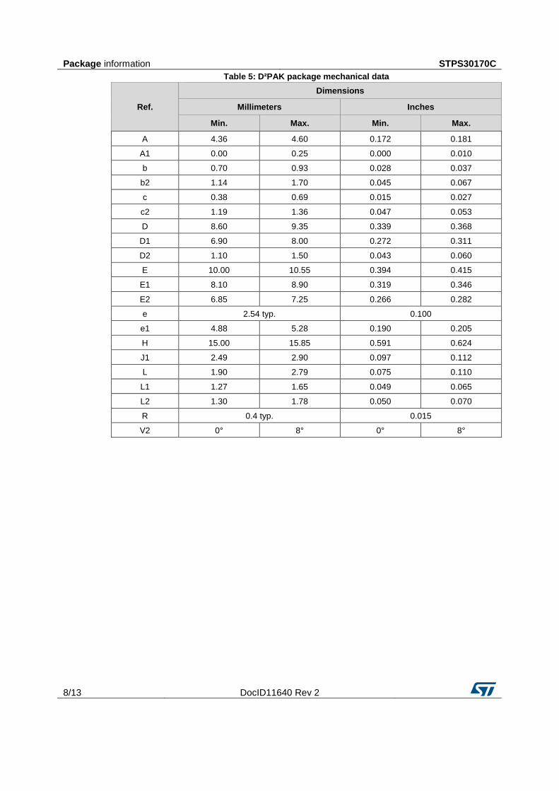
Table 5: D²PAK package mechanical data
Ref.
Dimensions
Millimeters Inches
Min. Max. Min. Max.
A 4.36 4.60 0.172 0.181
A1 0.00 0.25 0.000 0.010
b 0.70 0.93 0.028 0.037
b2 1.14 1.70 0.045 0.067
c 0.38 0.69 0.015 0.027
c2 1.19 1.36 0.047 0.053
D 8.60 9.35 0.339 0.368
D1 6.90 8.00 0.272 0.311
D2 1.10 1.50 0.043 0.060
E 10.00 10.55 0.394 0.415
E1 8.10 8.90 0.319 0.346
E2 6.85 7.25 0.266 0.282
e 2.54 typ. 0.100
e1 4.88 5.28 0.190 0.205
H 15.00 15.85 0.591 0.624
J1 2.49 2.90 0.097 0.112
L 1.90 2.79 0.075 0.110
L1 1.27 1.65 0.049 0.065
L2 1.30 1.78 0.050 0.070
R 0.4 typ. 0.015
V2 0° 8° 0° 8°

STPS30170C Package information
DocID11640 Rev 2 9/13
Figure 11: D²PAK recommended footprint (dimensions in mm)

Package information STPS30170C
10/13 DocID11640 Rev 2
2.2 TO-247 package information
Figure 12: TO-247 package outline
0075325_8

STPS30170C Package information
DocID11640 Rev 2 11/13
Table 6: TO-247 package mechanical data
Ref.
Dimensions
Millimeters Inches
Min. Typ. Max. Min. Typ. Max.
A 4.85
5.15 0.191
0.203
A1 2.20
2.60 0.086
0.102
b 1.00
1.40 0.039
0.055
b1 2.00
2.40 0.078
0.094
b2 3.00
3.40 0.118
0.133
c 0.40
0.80 0.015
0.031
D(1) 19.85
20.15 0.781
0.793
E 15.45
15.75 0.608
0.620
e 5.30 5.45 5.60 0.209 0.215 0.220
L 14.20
14.80 0.559
0.582
L1 3.70
4.30 0.145
0.169
L2
18.50
0.728
ØP(2) 3.55
3.65 0.139
0.143
ØR 4.50
5.50 0.177
0.217
S 5.30 5.50 5.70 0.209 0.216 0.224
Notes:
(1)Dimension D plus gate protusion does not exceed 20.5 mm (2)Resin thickness around the mounting hole is not less than 0.9 mm.

Ordering information STPS30170C
12/13 DocID11640 Rev 2
3 Ordering information Table 7: Ordering information
Order code Marking Package Weight Base qty Delivery mode
STPS30170CW STPS30170CW TO-247 4.40g 30 Tube
STPS30170CG-TR STPS30170CG D2PAK 1.48g 1000 Tape and reel
4 Revision history Table 8: Document revision history
Date Revision Changes
16-Sep-2005 1 First issue.
16-May-2017 2
Updated features, package silhouette and Table 1: "Device
summary".
Updated Section 1: "Characteristics", Section 1.1: "Characteristics
(curves)", Section 2: "Package information" and Table 7: "Ordering
information".

STPS30170C
DocID11640 Rev 2 13/13
IMPORTANT NOTICE – PLEASE READ CAREFULLY
STMicroelectronics NV and its subsidiaries (“ST”) reserve the right to make changes, corrections, enhancements, modifications , and improvements to ST products and/or to this document at any time without notice. Purchasers should obtain the latest relevant information on ST products before placing orders. ST products are sold pursuant to ST’s terms and conditions of sale in place at the time of order acknowledgement.
Purchasers are solely responsible for the choice, selection, and use of ST products and ST assumes no liability for application assistance or the design of Purchasers’ products.
No license, express or implied, to any intellectual property right is granted by ST herein.
Resale of ST products with provisions different from the information set forth herein shall void any warranty granted by ST for such product.
ST and the ST logo are trademarks of ST. All other product or service names are the property of their respective owners.
Information in this document supersedes and replaces information previously supplied in any prior versions of this document.
© 2017 STMicroelectronics – All rights reserved