Embed Size (px)
Citation preview
M. Wójcik, J. Gaca, P. Caban, ...
MATERIAŁY ELEKTRONICZNE (Electronic Materials), 2016, 44, 3 9
HRXRD study of ZnO single crystals bombarded with Ar ions
Marek Wójcik, Jarosław Gaca, Piotr Caban, Andrzej Turos Institute of Electronic Materials Technology
133 Wólczynska Str., 01-919 Warsaw, Poland e-mail: [email protected]
Abstract: High resolution X-ray diffraction methods (HRXRD) were used to study the tetragonalization of a unit cell in a zinc oxide single crystal resulting from the Ar-ion bombardment. Bulk ZnO (00∙1) single crystals were bombarded with ions with the energy of 300 keV and a dose range between 1 x 1014 cm-2 and 4 x 1016 cm-2. Diffraction profiles, obtained by radial 2Theta/Omega scans in the vicinity of the 00∙4 ZnO reciprocal space node were measured and fitted to the curves calculated by means of a computer program based on the Darwin’s dynamical theory of X-ray diffraction. On the basis of these numerical simulations, the profile of the interplanar spacing between planes perpendicular to the c axis of the ZnO single crystal were determined as a function of the Ar ion dose. It was found that positive deformation parallel to the c-axis appeared for the low doses in the bombarded crystal volume. When the dose is increased this deformation gets pronounced, and after reaching a certain critical value, it becomes saturated. This observation leads to the conclusion that the plastic deformation appears in the implanted volume of the crystal.
Key words: HRXRD, ZnO monocrystal, ion implantation, radiation defect analysis
Badanie metodami wysokorozdzielczej dyfraktometrii rentgenowskiej monokryształów ZnO bombardowanych jonami ArStreszczenie: Za pomocą wysokorozdzielczej dyfraktometrii rentgenowskiej (HRXRD) badano tetragonalizację komórki elementarnej monokryształu tlenku cynku powstałą pod wpływem bombardowania jonami Ar. Objętościowe mono-kryształy ZnO o orientacji (00∙1) były bombardowane jonami o energii 300 keV, w przedziale dawek od 1 x 1014 cm-2 do 4 x 1016 cm-2. Zarejestrowano profile dyfrakcyjne otrzymane metodą radialnego skanowania 2Teta/Omega, w otoczeniu węzła 00∙4, sieci odwrotnej ZnO i w oparciu o założenia dynamicznej teorii dyfrakcji promieniowania rentgenowskiego w ujęciu Darwina, wykonano ich symulacje numeryczne. Na tej podstawie określono, w zależności od dawki, profil zmiany odległości płaszczyzn prostopadłych do osi c monokryształu ZnO. Stwierdzono, że dla niskich dawek, w ściśle określonej objętości kryształu, powstaje dodatnie odkształcenie równoległe do osi c, wraz ze wzrostem dawki jonów to odkształcenie wzrasta, a po osiągnięciu pewnej krytycznej wartości ulega nasyceniu. To prowadzi do wniosku, że w implantowanej ob-jętości kryształu powstaje wówczas odkształcenie plastyczne.
Słowa kluczowe: wysokorozdzielcza dyfrakcja rentgenowska, monokryształ ZnO, implantacja jonów, analiza defektów radiacyjnych
open access
1. Introduction
ZnO is a wide bandgap energy (Eg = 3.37eV) semi-conductor. Its most important properties include direct and very high exciton binding energy (60 meV), strong piezoelectric effect, high conductivity, high heat capacity and low thermal expansion coefficient. Due to its wide potential application spectrum in microelectronics, bio-sensors, spintronics and light sources, ZnO has been the most intensively explored semiconductor material of the last decade [1]. Ion bombardment represents an attractive tool for semiconductor compound processing (doping, isolation etc.). However, a major drawback of this tech-nique is the buildup of lattice disorder due to the ballistic character of this process [2, 4]. Means that in spite of the vast amount of accumulated data, the mechanism of defect buildup in ZnO is not completely elucidated.
Damage accumulation in ion-bombarded compound semiconductors is a consequence of collision damage sequential evolution in extended defects such as disloca-tions or stacking faults. Our study of GaN [5 - 6] revealed
that damage accumulation is a three-step process. The HRXRD analysis indicated that ion bombardment to low doses causes an increase in the c parameter, thus leading to a strain buildup in the implanted region. Once the critical value of the shear stress is reached, plastic deformation due to the dislocation slip appears to take place, and as a result a dislocation tangle is formed. The transition to Stage III – amorphization – takes place at a high impurity concentration and is apparently due to the defect–impurity interaction.
2. Experimental
High-quality commercial [00∙1] single ZnO crystals delivered by MaTecK, Germany, were ion-bombarded at the Institute of Electronic Materials Technology (ITME) using the Balzers MBP 202RP ion implanter with 300 keV Ar+ ions to doses ranging from 1 x 1014 cm-2 to 1 x 1016 cm-2
at room temperature (RT). The structural characteristics of implanted ZnO monocrystals can be determined using
HRXRD study of ZnO single crystals bombarded with Ar ions
10 MATERIAŁY ELEKTRONICZNE (Electronic Materials), 2016, 44, 3,
d(x) = d0 (1 + μ exp ( — )),− 4 ln 2(x − x0)2
σ2
Fig. 1. X-ray diffraction profiles performing 2THETA/OMEGA scans for the virgin ZnO monocrystal implanted with doses ranging from 1 x 1012 cm-2 to 1 x 1016 cm-2.Rys. 1. Rentgenowskie profile dyfrakcyjne otrzymane metodą skanowania 2THETA/OMEGA dla monokryształu ZnO nieim-plantowaego, a także implantowanego dawkami od 1 x 1012 cm-2
do 1 x 1016 cm-2.
the non-destructive HRXRD method. To this end, the SmartLab diffractometer equipped with a 9 kW rotating Cu anode (wavelength CuKα1 equals 0.15405 nm) was used to perform the X-ray diffraction measurements. The radial 2Theta/Omega diffraction profiles were recorded for the following incident optics settings: cross beam optics CBO unit, Ge(220) x 2 monochromator, open soller slit, and on the receiving side: an open soller slit and soller slit of 5.0 deg. All measured samples were adjusted in such a way that the c-axis was parallel to the φ - axis of the goniometer. So as to obtain radial scans of the (00∙4) reci-procal lattice spot of the ZnO monocrystals. The resultant diffraction profiles are presented in Fig. 1.
The influence of implantation on the X-ray diffraction profile is strongly dependent on the ion dose. The shape of the 2Theta/Omega diffraction patterns in the vicinity of the 00∙4 reciprocal lattice spot of the implanted ZnO monocrystal, is characterized mainly by the asymmetry that appears on the low-angle side of the afore mentio-ned node. This asymmetry becomes greater when the dose of Ar ions becomes increased. A relatively high and well-separated peak appears for doses ranging from 1 x 1014 cm-2 to 2 x 1015 cm-2, on the low-angle side of the
00∙4 node while for the highest doses (e.g. 5 x 1015 cm-2 and 1 x 1016 cm-2) only some oscillations can be observed.
In order to study lattice deformation resulting from ion implantation, the collected experimental data were analyzed by means of computer simulations. The code, based on Darwin’s dynamical theory of X-ray diffrac-tion [7 - 8], was developed to perform X-ray diffraction profile simulation. For the purpose of such simulation, a heterostructure is modeled as a stack of parallel atomic planes. For each plane different chemical composition is assumed, which allows modeling graded hetero-in-terfaces. Based on the assumed chemical composition of the atomic planes, the code calculates the interplanar spacing between succeeding atomic planes and their scattering power. The diffraction profile for a crystal after ion irradiation can be calculated by displacing some of the atoms from their equilibrium positions in the atomic planes, and especially out of their position on the Bragg planes. This results in the modification of the interplanar atomic spacing and planar scattering power profiles [9]. The analysis is performed with the aim to diversify the chemical composition of each atomic plane (or planar scattering power and interplanar spacing) until the best fit between experimental and simulated X-ray diffraction profiles is achieved. The code was tested while working with AlxGa(1-x)As/GaAs superlattices to be applied as a Bragg mirror [10].
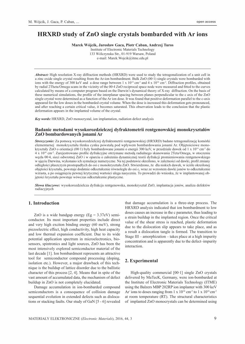
For the purpose of the simulation, the region of the ZnO monocrystal with the strain induced by ion irradiation was modeled as a stack of parallel layers, perpendicular to the c axis, each of which was 9 nm thick and differed in terms of interplanar spacing and/or planar scattering power. The profile of the interplanar spacing modulation in the growth direction was assumed to reproduce the shape of displaced atom distribution in ion-implanted ZnO [11 - 12]. This distribution was treated as the primary piece of data in X-ray profile calculations, and can be approximated by the Gaussian in the following form:
(1)
where:d(x) is the interplanar spacing between the (00∙4) planes in the strained layer, located at an x distance from the sur-face, d0 is the (00∙4) interplanar spacing in virgin ZnO, µ is the maximal lattice misfit between the strained lay-er and virgin ZnO, x0 is the position of the center of the Gaussian peak, and σ is the full width in the half maxi-mum of the standard distribution.
The fit between the experimental and calculated dif-fraction profiles was obtained by changing the values of the x0, σ and µ parameters (Fig. 2).
The examples of the best fits between the experimental and calculated diffraction profiles as well as strain profiles are shown in Fig. 3 - 7.
M. Wójcik, J. Gaca, P. Caban, ...
MATERIAŁY ELEKTRONICZNE (Electronic Materials), 2016, 44, 3 11
Fig. 2. Graded layer model of the strain distribution in the implanted region of the ZnO monocrystal.Rys. 2. Model rozkładu naprężeń w implantowanej objętości monokryształu ZnO.
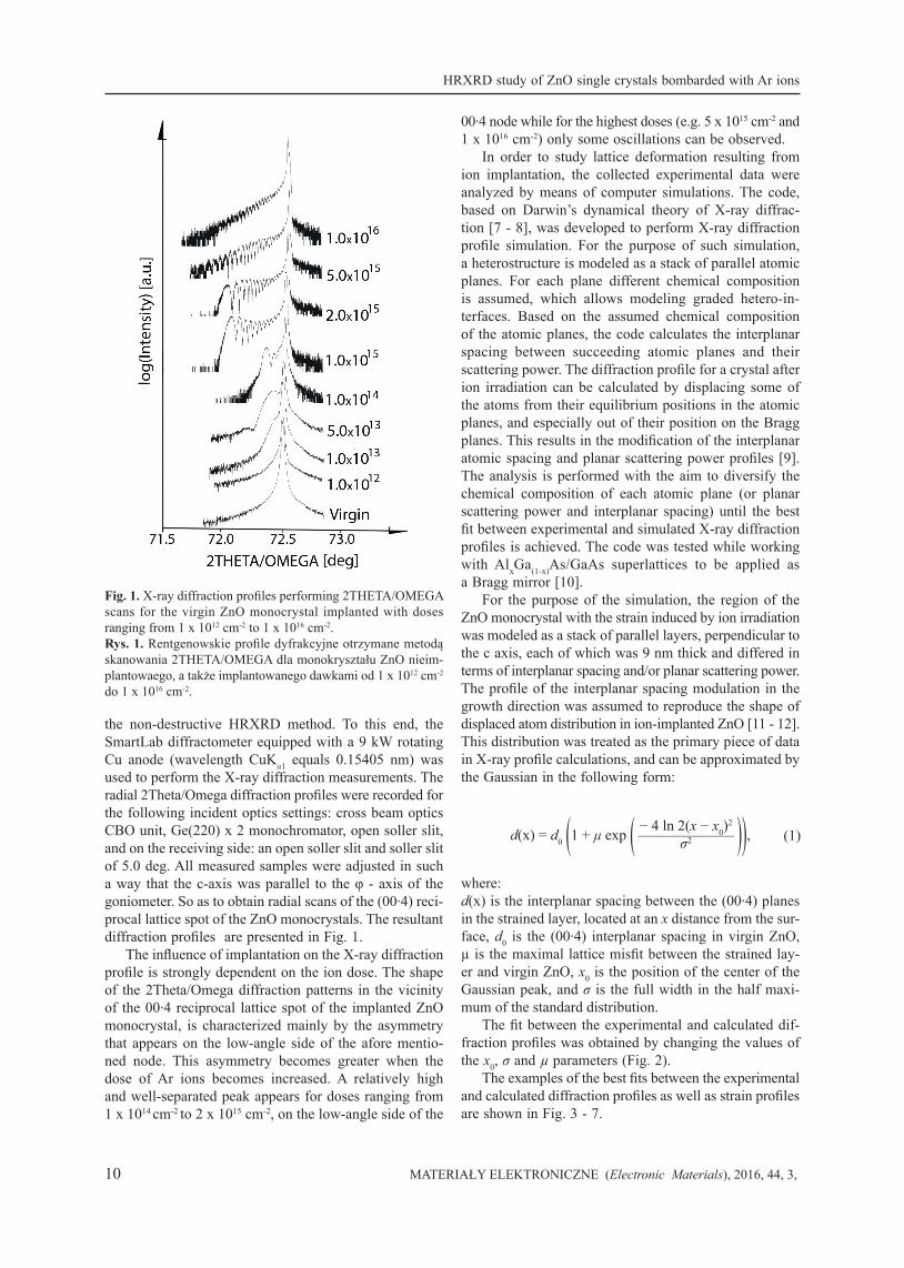
Fig. 3. X-ray diffraction profiles: experimental (solid) and calculated (dash) for the ZnO monocrystal implanted with the ion dose of 1 x 1013 cm-2. Reflection 00∙4, x0 = 180 nm, σ = 30 nm, <d> = 0,1301666 nm, µ = 0.015365.Rys. 3. Rentgenowskie profile dyfrakcyjne: doświadczalny (ciągły) i obliczony (przerywany) dla monokryształu ZnO implantowa-nego dawką 1 x 1013 cm-2. Refleks 00∙4, x0 = 180 nm, σ = 30 nm, <d> = 0,1301666 nm, µ = 0,015365.
Fig. 4. X-ray diffraction profiles: experimental (solid) and calculated (dash) for the ZnO monocrystal implanted with the ion dose of 1 x 1014 cm-2. Reflection 00∙4, x0=180 nm, σ = 100 nm, <d> = 0.1302327 nm, µ = 0.024200.Rys. 4. Rentgenowskie profile dyfrakcyjne: doświadczalny (ciągły) i obliczony (przerywany) dla monokryształu ZnO implantowa-nego dawką 1 x 1014 cm-2. Refleks 00∙4, x0 = 180 nm, σ = 100 nm, <d> = 0,1302327 nm, µ = 0,024200.
HRXRD study of ZnO single crystals bombarded with Ar ions
12 MATERIAŁY ELEKTRONICZNE (Electronic Materials), 2016, 44, 3,
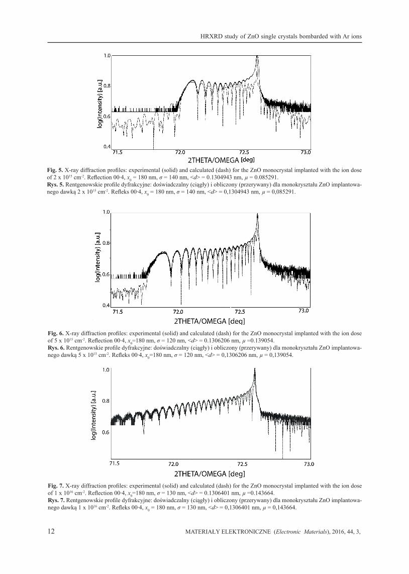
Fig. 5. X-ray diffraction profiles: experimental (solid) and calculated (dash) for the ZnO monocrystal implanted with the ion dose of 2 x 1015 cm-2. Reflection 00∙4, x0 = 180 nm, σ = 140 nm, <d> = 0.1304943 nm, µ = 0.085291.Rys. 5. Rentgenowskie profile dyfrakcyjne: doświadczalny (ciągły) i obliczony (przerywany) dla monokryształu ZnO implantowa-nego dawką 2 x 1015 cm-2. Refleks 00∙4, x0 = 180 nm, σ = 140 nm, <d> = 0,1304943 nm, µ = 0,085291.
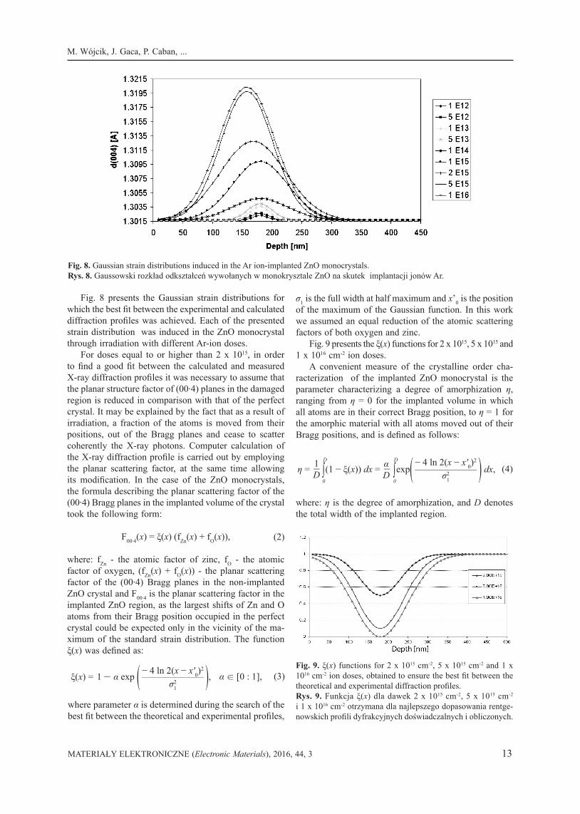
Fig. 6. X-ray diffraction profiles: experimental (solid) and calculated (dash) for the ZnO monocrystal implanted with the ion dose of 5 x 1015 cm-2. Reflection 00∙4, x0=180 nm, σ = 120 nm, <d> = 0.1306206 nm, µ =0.139054.Rys. 6. Rentgenowskie profile dyfrakcyjne: doświadczalny (ciągły) i obliczony (przerywany) dla monokryształu ZnO implantowa-nego dawką 5 x 1015 cm-2. Refleks 00∙4, x0=180 nm, σ = 120 nm, <d> = 0,1306206 nm, µ = 0,139054.
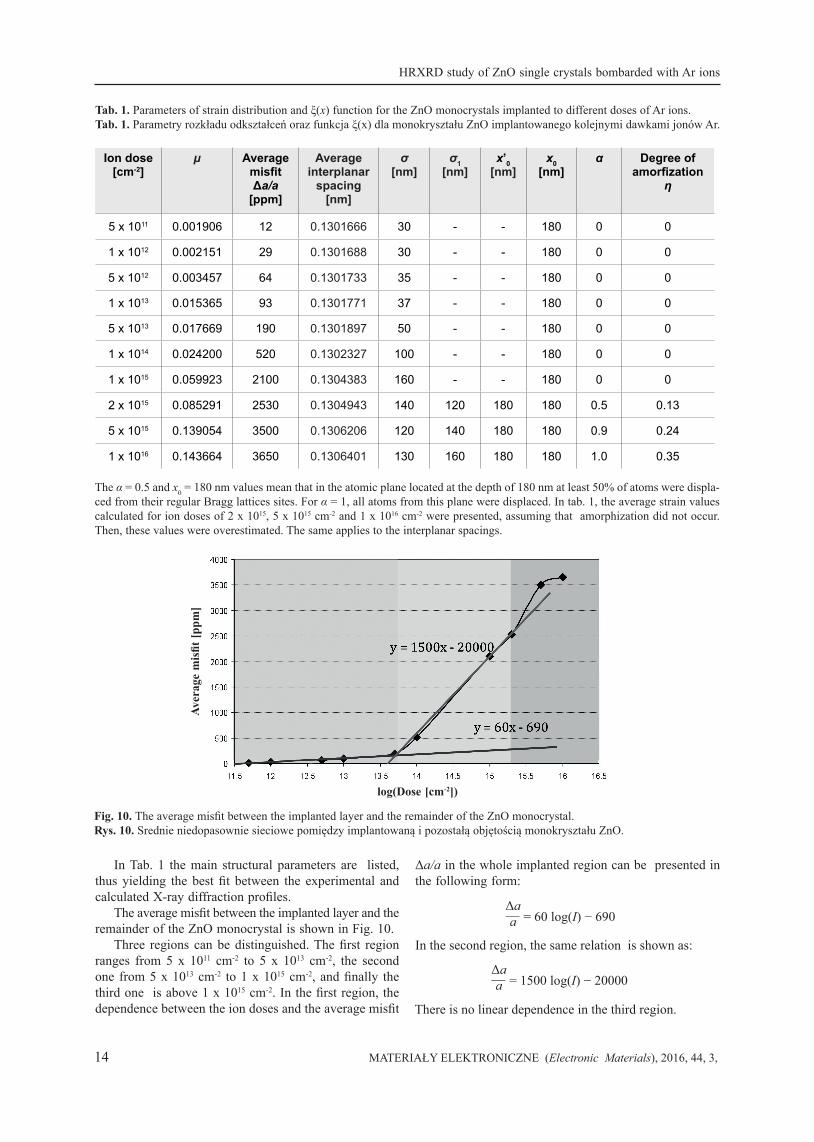
Fig. 7. X-ray diffraction profiles: experimental (solid) and calculated (dash) for the ZnO monocrystal implanted with the ion dose of 1 x 1016 cm-2. Reflection 00∙4, x0=180 nm, σ = 130 nm, <d> = 0.1306401 nm, µ =0.143664.Rys. 7. Rentgenowskie profile dyfrakcyjne: doświadczalny (ciągły) i obliczony (przerywany) dla monokryształu ZnO implantowa-nego dawką 1 x 1016 cm-2. Refleks 00∙4, x0 = 180 nm, σ = 130 nm, <d> = 0,1306401 nm, µ = 0,143664.
M. Wójcik, J. Gaca, P. Caban, ...
MATERIAŁY ELEKTRONICZNE (Electronic Materials), 2016, 44, 3 13
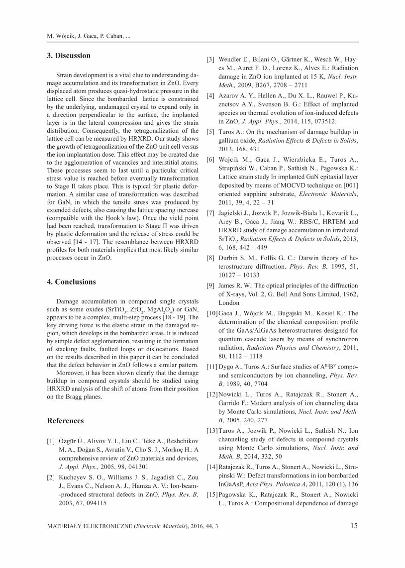
Fig. 8. Gaussian strain distributions induced in the Ar ion-implanted ZnO monocrystals.Rys. 8. Gaussowski rozkład odkształceń wywołanych w monokrysztale ZnO na skutek implantacji jonów Ar.
Fig. 8 presents the Gaussian strain distributions for which the best fit between the experimental and calculated diffraction profiles was achieved. Each of the presented strain distribution was induced in the ZnO monocrystal through irradiation with different Ar-ion doses.
For doses equal to or higher than 2 x 10¹⁵, in order to find a good fit between the calculated and measured X-ray diffraction profiles it was necessary to assume that the planar structure factor of (00∙4) planes in the damaged region is reduced in comparison with that of the perfect crystal. It may be explained by the fact that as a result of irradiation, a fraction of the atoms is moved from their positions, out of the Bragg planes and cease to scatter coherently the X-ray photons. Computer calculation of the X-ray diffraction profile is carried out by employing the planar scattering factor, at the same time allowing its modification. In the case of the ZnO monocrystals, the formula describing the planar scattering factor of the (00∙4) Bragg planes in the implanted volume of the crystal took the following form:
F00∙4(x) = ξ(x) (fZn(x) + fO(x)),
where: fZn - the atomic factor of zinc, fO - the atomic factor of oxygen, (fZn(x) + fO(x)) - the planar scattering factor of the (00∙4) Bragg planes in the non-implanted ZnO crystal and F00∙4 is the planar scattering factor in the implanted ZnO region, as the largest shifts of Zn and O atoms from their Bragg position occupied in the perfect crystal could be expected only in the vicinity of the ma-ximum of the standard strain distribution. The function ξ(x) was defined as:
(2)
− 4 ln 2(x − x'0)2 σ2
1
ξ(x) = 1 − α exp ( — ), α ∈ [0 : 1], (3)
where parameter α is determined during the search of the best fit between the theoretical and experimental profiles,
σ1 is the full width at half maximum and x’0 is the position of the maximum of the Gaussian function. In this work we assumed an equal reduction of the atomic scattering factors of both oxygen and zinc.
Fig. 9 presents the ξ(x) functions for 2 x 10¹⁵, 5 x 10¹⁵ and 1 x 1016 cm-2 ion doses.
A convenient measure of the crystalline order cha-racterization of the implanted ZnO monocrystal is the parameter characterizing a degree of amorphization η, ranging from η = 0 for the implanted volume in which all atoms are in their correct Bragg position, to η = 1 for the amorphic material with all atoms moved out of their Bragg positions, and is defined as follows:
η = − ∫D
0
(1 − ξ(x)) dx = − ∫D
0
exp( — ) dx,− 4 ln 2(x − x'0)2
σ21
1D
αD (4)
where: η is the degree of amorphization, and D denotes the total width of the implanted region.
Fig. 9. ξ(x) functions for 2 x 1015 cm-2, 5 x 1015 cm-2 and 1 x 1016 cm-2 ion doses, obtained to ensure the best fit between the theoretical and experimental diffraction profiles.Rys. 9. Funkcja ξ(x) dla dawek 2 x 1015 cm-2, 5 x 1015 cm-2 i 1 x 1016 cm-2 otrzymana dla najlepszego dopasowania rentge-nowskich profili dyfrakcyjnych doświadczalnych i obliczonych.
HRXRD study of ZnO single crystals bombarded with Ar ions
14 MATERIAŁY ELEKTRONICZNE (Electronic Materials), 2016, 44, 3,
In Tab. 1 the main structural parameters are listed, thus yielding the best fit between the experimental and calculated X-ray diffraction profiles.
The average misfit between the implanted layer and the remainder of the ZnO monocrystal is shown in Fig. 10.
Three regions can be distinguished. The first region ranges from 5 x 1011 cm-2 to 5 x 1013 cm-2, the second one from 5 x 1013 cm-2 to 1 x 1015 cm-2, and finally the third one is above 1 x 1015 cm-2. In the first region, the dependence between the ion doses and the average misfit
Ion dose [cm-2]
µ average misfit Δa/a
[ppm]
average interplanar
spacing [nm]
σ [nm]
σ1 [nm]
x’0 [nm]
x0 [nm]
α Degree of amorfization
η
5 x 10¹¹ 0.001906 12 0.1301666 30 - - 180 0 0
1 x 10¹² 0.002151 29 0.1301688 30 - - 180 0 0
5 x 10¹² 0.003457 64 0.1301733 35 - - 180 0 0
1 x 10¹³ 0.015365 93 0.1301771 37 - - 180 0 0
5 x 10¹³ 0.017669 190 0.1301897 50 - - 180 0 0
1 x 10¹⁴ 0.024200 520 0.1302327 100 - - 180 0 0
1 x 10¹⁵ 0.059923 2100 0.1304383 160 - - 180 0 0
2 x 10¹⁵ 0.085291 2530 0.1304943 140 120 180 180 0.5 0.13
5 x 10¹⁵ 0.139054 3500 0.1306206 120 140 180 180 0.9 0.24
1 x 10¹⁶ 0.143664 3650 0.1306401 130 160 180 180 1.0 0.35
Tab. 1. Parameters of strain distribution and ξ(x) function for the ZnO monocrystals implanted to different doses of Ar ions.Tab. 1. Parametry rozkładu odkształceń oraz funkcja ξ(x) dla monokryształu ZnO implantowanego kolejnymi dawkami jonów Ar.
The α = 0.5 and x0 = 180 nm values mean that in the atomic plane located at the depth of 180 nm at least 50% of atoms were displa-ced from their regular Bragg lattices sites. For α = 1, all atoms from this plane were displaced. In tab. 1, the average strain values calculated for ion doses of 2 x 10¹⁵, 5 x 1015 cm-2 and 1 x 1016 cm-2 were presented, assuming that amorphization did not occur. Then, these values were overestimated. The same applies to the interplanar spacings.
Fig. 10. The average misfit between the implanted layer and the remainder of the ZnO monocrystal.Rys. 10. Srednie niedopasownie sieciowe pomiędzy implantowaną i pozostałą objętością monokryształu ZnO.
Δa/a in the whole implanted region can be presented in the following form:
− = 60 log(I) − 690Δaa
In the second region, the same relation is shown as:
− = 1500 log(I) − 20000Δaa
There is no linear dependence in the third region.
log(Dose [cm-2])
Aver
age
mis
fit [p
pm]
M. Wójcik, J. Gaca, P. Caban, ...
MATERIAŁY ELEKTRONICZNE (Electronic Materials), 2016, 44, 3 15
3. Discussion
Strain development is a vital clue to understanding da-mage accumulation and its transformation in ZnO. Every displaced atom produces quasi-hydrostatic pressure in the lattice cell. Since the bombarded lattice is constrained by the underlying, undamaged crystal to expand only in a direction perpendicular to the surface, the implanted layer is in the lateral compression and gives the strain distribution. Consequently, the tetragonalization of the lattice cell can be measured by HRXRD. Our study shows the growth of tetragonalization of the ZnO unit cell versus the ion implantation dose. This effect may be created due to the agglomeration of vacancies and interstitial atoms. These processes seem to last until a particular critical stress value is reached before eventually transformation to Stage II takes place. This is typical for plastic defor-mation. A similar case of transformation was described for GaN, in which the tensile stress was produced by extended defects, also causing the lattice spacing increase (compatible with the Hook’s law). Once the yield point had been reached, transformation to Stage II was driven by plastic deformation and the release of stress could be observed [14 - 17]. The resemblance between HRXRD profiles for both materials implies that most likely similar processes occur in ZnO.
4. Conclusions
Damage accumulation in compound single crystals such as some oxides (SrTiO3, ZrO2, MgAl2O4) or GaN, appears to be a complex, multi-step process [18 - 19]. The key driving force is the elastic strain in the damaged re-gion, which develops in the bombarded areas. It is induced by simple defect agglomeration, resulting in the formation of stacking faults, faulted loops or dislocations. Based on the results described in this paper it can be concluded that the defect behavior in ZnO follows a similar pattern.
Moreover, it has been shown clearly that the damage buildup in compound crystals should be studied using HRXRD analysis of the shift of atoms from their position on the Bragg planes.
References
[1] Özgür Ü., Alivov Y. I., Liu C., Teke A., Reshchikov M. A., Doğan S., Avrutin V., Cho S. J., Morkoç H.: A comprehensive review of ZnO materials and devices, J. Appl. Phys., 2005, 98, 041301
[2] Kucheyev S. O., Williams J. S., Jagadish C., Zou J., Evans C., Nelson A. J., Hamza A. V.: Ion-beam--produced structural defects in ZnO, Phys. Rev. B, 2003, 67, 094115
[3] Wendler E., Bilani O., Gärtner K., Wesch W., Hay-es M., Auret F. D., Lorenz K., Alves E.: Radiation damage in ZnO ion implanted at 15 K, Nucl. Instr. Meth., 2009, B267, 2708 – 2711
[4] Azarov A. Y., Hallen A., Du X. L., Rauwel P., Ku-znetsov A.Y., Svenson B. G.: Effect of implanted species on thermal evolution of ion-induced defects in ZnO, J. Appl. Phys., 2014, 115, 073512.
[5] Turos A.: On the mechanism of damage buildup in gallium oxide, Radiation Effects & Defects in Solids, 2013, 168, 431
[6] Wojcik M., Gaca J., Wierzbicka E., Turos A., Strupiński W., Caban P., Sathish N., Pągowska K.: Lattice strain study In implanted GaN epitaxial layer deposited by means of MOCVD technique on [001] oriented sapphire substrate, Electronic Materials, 2011, 39, 4, 22 – 31
[7] Jagielski J., Jozwik P., Jozwik-Biala I., Kovarik L., Arey B., Gaca J., Jiang W.: RBS/C, HRTEM and HRXRD study of damage accumulation in irradiated SrTiO3, Radiation Effects & Defects in Solids, 2013, 6, 168, 442 – 449
[8] Durbin S. M., Follis G. C.: Darwin theory of he-terostructure diffraction. Phys. Rev. B, 1995, 51, 10127 – 10133
[9] James R. W.: The optical principles of the diffraction of X-rays, Vol. 2, G. Bell And Sons Limited, 1962, London
[10] Gaca J., Wójcik M., Bugajski M., Kosiel K.: The determination of the chemical composition profile of the GaAs/AlGaAs heterostructures designed for quantum cascade lasers by means of synchrotron radiation, Radiation Physics and Chemistry, 2011, 80, 1112 – 1118
[11] Dygo A., Turos A.: Surface studies of AIIIBV compo-und semiconductors by ion channeling, Phys. Rev. B, 1989, 40, 7704
[12] Nowicki L., Turos A., Ratajczak R., Stonert A., Garrido F.: Modern analysis of ion channeling data by Monte Carlo simulations, Nucl. Instr. and Meth. B, 2005, 240, 277
[13] Turos A., Jozwik P., Nowicki L., Sathish N.: Ion channeling study of defects in compound crystals using Monte Carlo simulations, Nucl. Instr. and Meth. B, 2014, 332, 50
[14] Ratajczak R., Turos A., Stonert A., Nowicki L., Stru-pinski W.: Defect transformations in ion bombarded InGaAsP, Acta Phys. Polonica A, 2011, 120 (1), 136
[15] Pagowska K., Ratajczak R., Stonert A., Nowicki L., Turos A.: Compositional dependence of damage

HRXRD study of ZnO single crystals bombarded with Ar ions
16 MATERIAŁY ELEKTRONICZNE (Electronic Materials), 2016, 44, 3,
buildup in Ar-ion bombarded AlGaN, Vacuum, 2009, 83, S145 – S147
[16] Guziewicz E., Kowalik A., Godlewski M., Ko-palko K., Osinniy V., Wójcik A., Yatsunenko S., Łusakowska E., Paszkowicz W., Guziewicz M. et al.: Extremely low temperature growth of ZnO by atomic layer deposition, J. Appl. Phys., 2008, 103, 3, 033515
[17] Turos A., Gaca J., Wojcik M., Nowicki L., Ratajczak R., Groetzschel R., Eichhorn F., Schell N.: Virtues and pitfalls in structural analysis of compound se-miconductors by the complementary use of RBS/channeling and high resolution X-ray diffraction,
Nuclear Instruments and Methods in Physics Rese-arch B, 2004, 219 – 220, 618 – 625
[18] Devaraju G., Dhamodaran S., Pathak A. P., Sarava-nan S. G., Gaca J., Wojcik M., Turos A., Khan S. A., Avasthi D. K., Arora B. M.: Ion beam modification of strained InGaAs/InP characterized by HRXRD, PL and AFM, Nuclear Instruments and Methods in Physics Research B, 2008, 266, 3552 – 355
[19] Eichhorn F., Gaca J., Heera V., Schell N., Turos A., Weishart H., Wojcik M.: Structural studies on ion--implanted semiconductors using X-ray synchrotron radiation:Strain evolution and growth of nanocry-stals, Vacuum, 2005, 78, 303 – 309