Embed Size (px)
Citation preview
Research ArticleInvestigation of the Optical and Electrical Properties of ITOZnOCdSCuOCoAg Structure for Solar Cell
L Nkhaili 1 A Narjis1 A Outzourhit1 A El Kissani1 and R El Moznine2
1Nanomaterials for Energy and Environment Laboratory Physics Department Faculty of Sciences SemlaliaCadi Ayyad University PO Box 2390 Marrakech 40000 Morocco2Laboratory Physics of Condensed Matter Chouaib Doukkali University El-Jadida Morocco
Correspondence should be addressed to L Nkhaili lahcencomhotmailfr
Received 21 April 2020 Accepted 24 June 2020 Published 17 July 2020
Academic Editor Hom Kandel
Copyright copy 2020 L Nkhaili et al (is is an open access article distributed under the Creative Commons Attribution Licensewhich permits unrestricted use distribution and reproduction in any medium provided the original work is properly cited
In this work a new structure ITOn-ZnOn-CdSp-CuOCoAg for solar cell was prepared on a glassITO substrate (e RF sputteringwas used to deposit the window layer (n-ZnO) at different time periods in order to reach various thickness of this film(e n-CdS thinfilms were synthesized by sol-gel technique to reduce the energy bands(e buffer layer (p-CuOCo) was sputtered at 200W under 30of oxygen(en the electrode (Ag) with a thickness of 100nmwas deposited by thermal evaporation under a pressure of 10minus5mbar(ephotovoltaic activity results obtained from this structure showed that the above method is more relevant to achieve such structure (eelectrical properties of this structure were investigated using the current-voltage (I-V) and AC impedance complex measurements (evalues of open circuit voltage (Voc) short-circuit current (Jsc) and fill factor (FF) are 046V 41mAcmminus2 and 30 respectively (eanalysis of complex impedancemeasurements was very useful to investigate the electrical behavior of n-ZnOn-CdS and n-CdSp-CuOCo interfaces(e impedance data are presented in theNyquist and Bode plots at different thicknesses of the n-ZnOfilms An equivalentcircuit was used to analyze and to fit the experimental data (e validity of these fitting results is further supported by the extrapolationand the deconvolution of both process of the diffusion and recombination processes at the n-ZnOn-CdS and n-CdSp-CuOCointerfaces respectively Our finding could provide an efficientmethod for fabricating a new configuration for improving the efficiency ofinorganic ZnOCuO solar cells as well as a useful approach for the analysis of complex impedance measurements Further works are inprogress in order to better improve the conversion efficiency
1 Introduction
During the last decades solar cell technology has attracted theintention of many researchers(e best is not only to improvethe efficiency of solar cells but also to prepare devices at a lowcost (us it is sought to replace the silicon and germaniumby low-cost semiconductors Cuprous oxide (CuO) is anontoxic p-type semiconductor material with abundant soilwith optical band gap around 1 5 eV [1 2] cuprous oxide canact as a light absorber in heterojunction or tandem solar cells
Copper-based oxides have promising electrical optical andmanufacturing characteristics that establish this family ofmaterials as well suited for semiconductor P For this reasonCuO thin films can be obtained by different techniques such assol-gel [3] thermal evaporation [4] electrodeposition [5] andradiofrequency (RF) sputtering technique [6]
Our previous work [1 7] was carried out on theheterojunctions based on ZnO and CuO However a lowconversion efficiency was obtained close to 001(erefore the current work focused on the insertion ofCdS is expected to facilitate the transport of photo-generated charge porters and the doping of the CuO bycobalt according to the optimization achieved by ourresearch group [8] in view to improve the conversionefficiency
In this paper the ITOZnOCdSCoCuOAg heter-ojunction is prepared for the first time by the RF sput-tering and spin-coating methods on indium tin oxide(ITO) substrates Our aim is to study the effect ofthickness of the ZnO film by analyzing data from opticalmeasurements and electrochemical impedance spectros-copy (EIS)
HindawiAdvances in Materials Science and EngineeringVolume 2020 Article ID 3907203 8 pageshttpsdoiorg10115520203907203
2 Experimental Detail
ZnO window layers were deposited on glassITO substratesby reactive RF-sputtering in an ALCATEL SCM 451 de-position system equipped with an ALCATEL ARF 601 RFgenerator operating at 1356MHz (e ZnO thin film wasthen deposited at 200W as a RF power at different times 1020 and 30min (e sputtering was out in a gas mixture(argon oxygen) with 30 of O2
CdS thin films were synthesized on ITOZnO substratesin acitone using cadmium chloride (CdCl2 01M) andthiourea (CH4N2S 01M) as precursors then after thin filmswere deposited by the spin-coating method at 2200 rpm for1min finally the thin films were baked on a hot plate for10min to obtain the yellow color [9] (e CuOCo thin filmwas deposited using an RF power of 150W for 90min (eseparameters were obtained and used based on our previousoptimization of the deposition conditions [8] At the end thestructure was completed by depositing Ag dots on the surfaceof the copper oxide by thermal evaporation
(e optical properties were measured using a Shimadzu-3101-UVPC double beam spectrophotometer in the wave-length range 200ndash3200 nm(e electrical junction propertieswere investigated by current-voltage (I-V) characteristics
(e electrochemical impedance spectroscopy (EIS) wasperformed using a Solartron impedance analyzer model 1260A(emeasurements were carried out in the frequency range from1Hz to 1MHz using the AC voltage at 50mV SMaRTsoftwarewas used via a general-purpose interface and Zview softwarewas used to fit and to investigate the impedance data
3 Results and Discussion
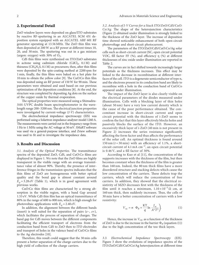
31 Analysis of the Optical Properties (e transmittancespectra of the deposited ZnO CdS and CuOCo films aredisplayed in Figure 1 We note that the ZnO films are highlytransparent in the visible range with an average transmit-tance value of almost 90 (ereby the presence of inter-ference fringes in the transmission spectra indicates that thethin films of ZnO are homogeneous with better opticalquality and the bond gap is almost constant aroundEg 328 eV (Table 1) which is in good agreement withprevious works
CuOCo thin films are characterized by a strong ab-sorption in the visible region with a band Gap around153 eV While CdS thin film has an optical transmittance of80 in the range of 600 to 800 nm which is high enough forphotovoltaic applications with Eg 240 eV
In addition the alignment between the different bands(insert) is well suited for the separation of pairs (eminus e+)which facilitates the process of separation of charges (eband gap for CdS moves between the different componentsfacilitating the efficient transport of electrons from theconduction band from CdS to ZnO then to ITO electrodesand transport of holes in the valence band of CuOCo filmsto the Ag electrodes [10]
(erefore this result could suggest that the 30min cellspresent a better separation of the charge carriers due to thehigh yield of collection of the charge carriers
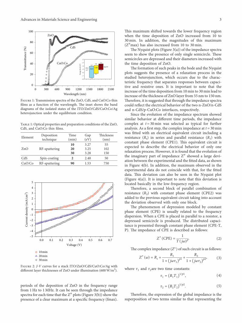
32 Analysis of J-V Curves for a Stack ITOZnOCdSCuOCoAg (e shape of the heterojunction characteristics(Figure 2) obtained under illumination is strongly linked tothe thickness of the ZnO layer (e increase of depositiontime showed noticeable enhancement of both open-circuitphotovoltage and short-circuit photocurrent
(e parameters of the ITOZnOCdSCuOCoAg solarcells such as short-circuit current JSC open circuit potentialVOC fill factor FF () and efficiency η () at differentthicknesses of zinc oxide under illumination are reported inTable 2
(e curves are in fact shifted towards increasingly largerpotentials as the thickness increases (is effect may belinked to the decrease in recombination at different inter-faces of the cell ITO is a degenerate semiconductor of type nand the electrons present in its conduction band are likely torecombine with a hole in the conduction band of CuOCoappeared under illumination
(e impact of the ZnO layer is also clearly visible onthe electrical parameters of the diodes measured underillumination Cells with a blocking layer of thin holes(about 50 nm) have a very low current density which isthe cause of the poor performance obtained (e con-comitant increase in short-circuit current and opencircuit potential with the thickness of i-ZnO seems toconfirm the fact that this layer effectively blocks holes andpassively blocks the surface of the ITO However anexcessively thick layer of i-ZnO (40 min is not present inFigure 2) increases the series resistance significantlyaffecting the form factor and thus affects the performanceof the solar cell An optimal thickness is found around150 nm (t 30min) with an efficiency of 11 a short-circuit current of 41 mA cmminus2 an open circuit potentialis 046 V and a fill factor of 30
According to Kuo et al [11] the concentration of thesupports increases with the thickness of the film but thenbecomes constant when the thickness of the film is greaterthan 160 nm Indeed the 80 nm thick films have a moredisordered structure and stacking defects which cause thelow concentration of the carriers (ese defects trap thecarriers which will reduce the concentration of freecarriers In addition they showed that the electrical re-sistivity of MZO decreases first with the thickness of thefilm until it reaches a minimum 110 times10minus3Ω cm at160 nm thick then suddenly increases (us the cells of30min have a better concentration of carriers with a lowresistivity
Voc n ΦB +KTq
lnJsc
AlowastT21113888 1113889 (1)
Hence the increase in VOC as a function of the thicknessof ZnO is due to the increase in the barrierΦB (equation (1))due to the high concentration of the too thick layers
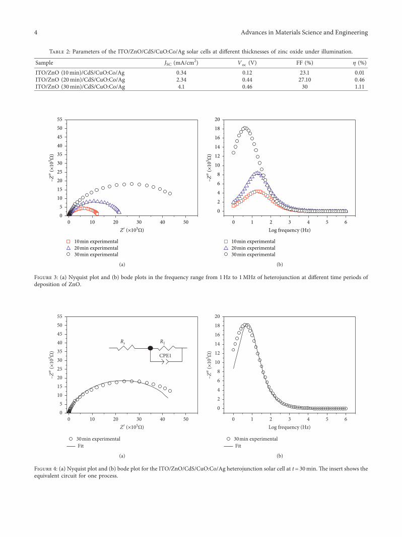
33 Electrochemical Impedance Spectroscopy (EIS)Figure 3 show the evolutions of impedance spectra of theITOZnOCdSCuOCoAg heterojunction at different time
2 Advances in Materials Science and Engineering
periods of the deposition of ZnO in the frequency rangefrom 1Hz to 1MHz It can be seen through the impedancespectra for each time that the ZPrime plots (Figure 3(b)) show thepresence of a clear maximum at a specific frequency (fmax)
(is maximum shifted towards the lower frequency regionwhen the time deposition of ZnO increased from 10 to30min In addition the magnitudes of this maximum(ZPrimemax) has also increased from 10 to 30min
(e Nyquist plots (Figure 3(a)) of the impedance spectraseem to show the presence of only single semicircle (esesemicircles are depressed and their diameters increased withthe time deposition of ZnO
(e formation of such peaks in the bode and the Nyquistplots suggests the presence of a relaxation process in thestudied heterojunction which occurs due to the charac-teristic frequency that separates responses between capaci-tive and resistive ones It is important to note that theincrease of the time deposition from 10min to 30min lead toincrease of the thickness of ZnO layer from 55 nm to 150 nm(erefore it is suggested that through the impedance spectracould reflect the electrical behavior of the two n-ZnOn-CdSand n-CdSp-CuOCo interfaces respectively
Since the evolution of the impedance spectrum showedsimilar behavior at different time periods the impedancecomplex at t 30min was selected as typical for furtheranalysis As a first step the complex impedance at t 30minwas fitted with an electrical equivalent circuit including aresistance (Rs) in series and parallel resistance (R1) withconstant phase element (CPE1) (is equivalent circuit isexpected to describe the electrical behavior of only onerelaxation process However it is found that the evolution ofthe imaginary part of impedance ZPrime showed a large devi-ation between the experimental and the fitted data as shownin Figure 4(b) In addition the maximum observed in theexperimental data do not coincide with that for the fitteddata (is deviation can also be seen in the Nyquist plot(Figure 4(a)) It is important to note that this deviation islocated basically in the low-frequency region
(erefore a second block of parallel combination ofresistance (R2) with constant phase element (CPE2) wasadded to the previous equivalent circuit taking into accountthe deviation observed with only one block
(e phenomenon of depression modeled by constantphase element (CPE) is usually related to the frequencydispersion When a CPE is placed in parallel to a resistor adepressed semicircle is produced (e distributed capaci-tance is presented through constant phase element (CPE-TP) (e impedance of CPE is described as follows
Zlowast(CPE)
1T(jω)p (2)
(e complex impedance (Zlowast) of such circuit is as follows
Zlowast(ω) Rs +
R1
1 + jωτ1( 1113857p1 +
R2
1 + jωτ2( 1113857p2 (3)
where τ1 and τ2are two time constants
τ1 R1T1( 11138571p1
(4)
τ2 R2T2( 11138571p2
(5)
(erefore the expression of the global impedance is thesuperposition of two terms similar to that representing the
75
62
515
Ag48
3438
42
ITO47
ZnOCdS
CuOCo
ZnO
CdS
CuOCo
0
20
40
60
80
100
Tran
smitt
ance
()
300 600 900 1200 1500 1800 21000Wavelength (nm)
ndash8
ndash7
ndash6
ndash5
ndash4
ndash3
ndash2
Ener
gy le
vel (
eV)
Figure 1 Transmission spectra of the ZnO CdS and CuOCo thinfilms as a function of the wavelength (e inset shows the banddiagrams of the isolated states of the ITOZnOCdSCuOCoAgheterojunction under the equilibrium condition
Table 1 Optical properties and preparation conditions of the ZnOCdS and CuOCo thin films
Element Depositiontechnique
Time(min)
Gap(eV)
(ickness(nm)
ZnO RF-sputtering10 327 5520 325 10230 328 150
CdS Spin-coating 2 240 50CuOCo RF-sputtering 90 153 750
10min20min30min
ndash5ndash4ndash3ndash2ndash1
012345
Curr
ent d
ensit
y (m
Ac
m2 )
01 02 03 04 05 06 0700Voltage (V)
Figure 2 J-V curves for a stack ITOZnOCdSCuOCoAg withdifferent layer thicknesses of ZnO under illumination (600Wm2)
Advances in Materials Science and Engineering 3
10min experimental20min experimental30min experimental
05
10152025303540455055
ndashZPrime
(times10
5 Ω)
10 20 30 40 500Zprime (times105Ω)
(a)
10min experimental20min experimental30min experimental
0
2
4
6
8
10
12
14
16
18
20
ndashZPrime
(times10
5 Ω)
1 2 3 4 5 60Log frequency (Hz)
(b)
Figure 3 (a) Nyquist plot and (b) bode plots in the frequency range from 1Hz to 1MHz of heterojunction at different time periods ofdeposition of ZnO
30min experimentalFit
05
10152025303540455055
ndashZPrime
(times10
5 Ω)
10 20 30 40 500Zprime (times105Ω)
Rs R1
CPE1
(a)
30min experimentalFit
0
2
4
6
8
10
12
14
16
18
20
ndashZPrime
(times10
5 Ω)
1 2 3 4 5 60Log frequency (Hz)
(b)
Figure 4 (a) Nyquist plot and (b) bode plot for the ITOZnOCdSCuOCoAg heterojunction solar cell at t 30min (e insert shows theequivalent circuit for one process
Table 2 Parameters of the ITOZnOCdSCuOCoAg solar cells at different thicknesses of zinc oxide under illumination
Sample JSC (mAcm2) Voc (V) FF () η ()
ITOZnO (10min)CdSCuOCoAg 034 012 231 001ITOZnO (20min)CdSCuOCoAg 234 044 2710 046ITOZnO (30min)CdSCuOCoAg 41 046 30 111
4 Advances in Materials Science and Engineering
ColendashCole relaxation in the complex permittivity formalism(equation (6)) [12]
εlowast(ω) εinfin +Δε
1 + jωτε( 1113857α (6)
where εs and εinfin are the low-frequency and the high-fre-quency dielectric constants values respectively τ is therelaxation time Δε is the dielectric strength (Δε εs minus εinfin)and α is an exponent between 0 and 1
According to the above expression the compleximpedance the evolution of the imaginary part Z as afunction of the angular frequency is expected to show amaximum at a critical angular frequency (ωmax) (ere-fore the derivation ((dZPrime(ω)dω) 0) of the imaginarypart ZPrime with the respect of angular frequency (ω) can beused in order to find this critical angular frequency
(e above equation leads to obtain tow relationship forthe angular frequency (ω1max) and (ω2max)
ω1max 1τ1
ω2max 1τ2
(7)
(is circuit includes position independent distributedcircuit elements relating to the transport resistance (Rt R1)recombination resistance (Rrec R2) and chemical capaci-tance (CPE constant phase element) that are accounting forthe homogeneous charge carrier transport electron holerecombination and capacitance per unit area due to chargeaccumulation associated with ITOZnOCdSCuOCoAgrespectively [13] An additional resistance (Rs) appears in theequivalent circuit attributed to the additional contribution ofthe series resistance (is equivalent circuit produces a goodfit to the experimental data for the typical solar cell preparedat t 30min as it is shown in Figure 5 Moreover an ex-trapolation in the low-frequency region up to F 10minus2 Hzwas carried out to follow the trend of the real Zprime and theimaginary part ZPrime of the complex impedance (en aseparation andor deconvolution of the two processes wereemployed to further investigate the contribution and theidentification of each process
In the Nyquist plot (Figure 5(a)) the real part Zprime of theimpedance can be explained through three resistances (efirst is found in the low-frequency region and it is corre-sponding to the recombination resistance (R2 Rrec) (esecond is attributed to transfer resistance (R1 Rt) in themedium frequency region while the high frequency regionis corresponding to series resistance (Rs)
(ese cases can be observed and checked from theNyquits plot where the values of R1 and R2 are the in-tercepts (e diameters of the two semicircles are cor-responding to the diffusion and the recombinationprocess at the two interfaces of the heterojunction
(e existence of the two processes is well confirmedby the deconvolution as it is shown in Figure 5(b) on theevolution of the imaginary part ZPrime as a function of fre-quency (erefore as it can be confirmed through this
approach that one can see that there are two both pro-cesses of diffusion and recombination which could reflectvery well the electrical behavior of the two n-ZnOn-CdSand n-CdSp-CuO interfaces respectively (e diffusionand recombination processes are related to n-ZnOn-CdSand n-CdSp-CuO interfaces (e validity of these resultsis further supported by the extrapolation and deconvo-lution of both processes at the low and high frequency
(e equivalent circuit produces a good fit (Figure 6) tothe experimental data (e fitting values of different ele-ments in the equivalent circuit given in Figure 7 were re-ported in Table 3
(e diffusion time (τd) and the recombination time τncorresponding to the effective electron lifetime before therecombination were calculated using the relationshipextracted from equations (4) and (5) for the compleximpedance
(e values of the diffusion time (τd) and lifetime (τn) aswell as the charge collection efficiency (ηcol) and the dif-fusion length (Ld) are plotted in histogram (Figure 8)
(e obtained tn increase significantly from 111ms for(ITOZnO (10min)CdSCuOCoAg) to 513ms for ITOZnO (30min)CdSCuOCoAg by varying the thickness ofZnO (is result could suggest that the charge recombina-tion is highly reduced in the ZnO (30min) and the electron-hole separation [14]
(e time constant of the charge diffusion is also expectedto decrease with the increase of the time of the deposition ofZnO layer andor the thickness of ZnO layer In contrastthis later showed the inverse behavior resulting in an in-crease with the time (from 186 to 806ms for 10 up to30min) However this increases still very low in comparisonwith the time constant of the charge recombination (iscould be explained probably by the formation of a very thinlayer of silver oxide Ag2O3 between the active layer andcontact Ag due to the oxidation of the Ag layer because theconditions for preparing the evaporator was not enough toreach 10minus5mbar In these cases the injection of electronstowards Ag can be blocked by this barrier and can limit thecollection of charges (is defect could also explain theraison for reaching low conversion efficiency Similar be-havior was observed by Gupta et al [13] in their study ondegradation analysis of polymerfullerene solar cells due todo formation of Al2O3 the interface between aluminium andpolymer
(e charge collection efficiency ηcol and the diffusionlength Ld can be calculated from the Rrec and Rt values from[15]
ηcol 1 minusRt
Rrec (8)
Ld d timesRrec
Rt
1113888 1113889
12
(9)
(e charge collection efficiency ηcol and the diffusionlength Ld showed a very significant increase when thetime of the deposition increased
Advances in Materials Science and Engineering 5
(e growth in the collection yield of photo-generatedcarriers (ηcol) with the time of deposition as it is reported inTable 3 could also explain the increase in JSC value obtainedfrom J-V data as it is reported in the previous section inTable 2
(is behavior can be supported by the fact that the valuesof the diffusion length Ld (equation (9)) are greater than thethickness of the ZnO layer (d) (us the majority of photo-generated carriers can reach the ITO before recombining
It appears that the increase in Voc is due to an increasein the density of photoelectrons in an open circuit sit-uation which is mainly due to the growth of τn Con-sequently this result supports that the diffuse interfacebetween the components of CuOCo solar cell yieldhigher efficiency due to easier transport processes (ecombined effect of fast electron transport longer electronlifetime and lower recombination rate collectively im-prove the Jsc of the heterojunction [16]
55504540353025201510
50
0 10 20 30 40 50Zprime (times105Ω)
ndashZPrime
(times10
5 Ω)
10min experimental20min experimental
30min experimentalFit
(a)
201816141210
86420
0 1 2 3 4 5 6Log frequency (Hz)
ndashZPrime
(times10
5 Ω)
10min experimental20min experimental
30min experimentalFit
(b)
Figure 6 (a) Nyquist plot and (b) bode plots in the frequency range from 1Hz to 1MHz of heterojunction at different time periods ofdeposition of ZnO solid line represent the fit
Rs R1
CPE1 CPE2
R2
Figure 7 Equivalent circuit used to fit experimental data of the impedance spectrum at different time periods
55504540353025201510
50
0 10 20 30 40 50Zprime (times105Ω)
ndashZPrime
(times10
5 Ω)
Process HFProcess LF
1Hz
10ndash2Hz1MHz
30min experimental30min extrapolation
(a)
201816141210
86420
0 1ndash1 2ndash2 3 4 5 6Log frequency (Hz)
ndashZPrime
(times10
5 Ω)
Process HFProcess LF
Fn Fd
30min experimental30min extrapolation
(b)
Figure 5 (a) Nyquist and (b) bode plots for the ITOZnOCdSCuOCoAg at t 30min Deconvolution low frequency (red color) andhigh frequency (blue color)
6 Advances in Materials Science and Engineering
4 Conclusion
RF-sputtered ZnO thin films were successfully preparedusing a zinc metallic target and the effect of the thickness ofZnO window layer on the solar cell properties was inves-tigated (e optimal time for the deposition was observed tobe 30min at a RF power 200Wwith 30 of O2(erefore anoptimal thickness was found around 150 nm which lead toobtaining an efficiency of 11 short-circuit currentJsc 41mA cmminus2 open circuit potential Voc 046V and afill factor of 30 (Table 2)
(e electrochemical impedance spectroscopy (EIS)allowed us to investigate and to identify the diffusion andrecombination processes related to n-ZnOn-CdS andn-CdSp-CuO interfaces (e transfers and the recombi-nation resistance as well as the lifetime of the charge carrierswere extracted from the equivalent electrical circuit (echange that occurred with the increase of window layerthickness ZnO of all these parameters reflected very well theelectrical behavior of each interface
(is approach can be considered a good opportunity toprepare mainly oxide-based devices for photovoltaic ap-plications Indeed these first results could make the het-erojunction (ITOZnOCdSCuOCoAg) as a goodcandidate for solar cell It is important to state that the
achieved efficiency was carried out using only a small valueof illumination (erefore another study is in progress onthe same structure using the standard illumination AM 15Further studies are also expected to find the optimal ab-sorber layer thickness in order to reach the best conversionefficiency as well as the addition of doped Al-ZnO for re-ducing further the series resistance
Data Availability
(e characterization data and experimental results used tosupport the findings of this study are included within thearticle
Conflicts of Interest
(e authors declare that there are no conflicts of interestregarding the publication of this paper
References
[1] L Nkhaili M Elyaagoubi A Elmansouri et al ldquoStructuraloptical and electrical characteristics of zinc oxide and copperoxide films and their heterojunctionsrdquo Spectroscopy Lettersvol 48 no 7 pp 536ndash541 2015
Table 3 Parameters from the fitting with the equivalent circuit for the ITOZnOCdSCuOCoAg heterojunction solar cell
ITOZnOCdSCuOCo
dZnO(nm)
RS(Ω)
Rt R1(105Ω)
CPE1-T(10minus8F) CPE1-P Diffusion
time td (ms)Rrec R2(105Ω)
CPE2-T(10minus8F)
CPE2-P
Lifetime tn(ms)
η col()
Ld(nm)
ZnO(10min) 55 85 268 122 091 186 944 185 090 111 7006 10322
ZnO(20min) 102 6720 441 166 098 662 1810 158 086 129 7564 20664
ZnO(30min) 150 4277 812 098 1 802 446 195 082 513 8177 35134
ZnO (10min) ZnO (20min) ZnO (30min)
Charge collection efficiency ηcol ()Diffusion length Ld (nm)
Diffusion time τd (ms)Lifetime τn (ms)
Figure 8 Evolution of parameters for the ITOZnOCdSCuOCoAg heterojunction at different thicknesses of zinc oxide
Advances in Materials Science and Engineering 7
[2] B Balamurugan and B R Mehta ldquoOptical and structuralproperties of nanocrystalline copper oxide thin films preparedby activated reactive evaporationrdquo ltin Solid Films vol 396no 1-2 pp 90ndash96 2001
[3] A Yildiz S Horzum N Serin and T Serin ldquoHoppingconduction in In-doped CuO thin filmsrdquo Applied SurfaceScience vol 318 pp 105ndash107 2014
[4] M F Al-Kuhaili ldquoCharacterization of copper oxide thin filmsdeposited by the thermal evaporation of cuprous oxide(Cu2O)rdquo Vacuum vol 82 no 6 pp 623ndash629 2008
[5] N V Desai D D Shivagan L A Ekal and S H Pawar ldquoRoleof room-temperature electrochemical oxidation in Pb-dopedBi-Sr-Ca-CuO superconducting thin filmsrdquo MaterialsChemistry and Physics vol 65 no 1 pp 68ndash73 2000
[6] M Verma V Kumar and A Katoch ldquoSputtering basedsynthesis of CuO nanoparticles and their structural thermaland optical studiesrdquo Materials Science in SemiconductorProcessing vol 76 pp 55ndash60 2018
[7] L Nkhaili A El Kissani M Ait Ali et al ldquoEffect of RF poweron the structural and optical properties of RF-sputtered ZnOthin filmsrdquo lte European Physical Journal Applied Physicsvol 66 no 3 Article ID 30302 2014
[8] H El Aakib Elaboration of thin layers of copper oxide andcobalt oxide for the photothermal conversion of solar energyPhD thesis University Cadi Ayyad Marrakech Morocco2019
[9] A El Kissani H Ait Dads S Oucharrou et al ldquoA facile routefor synthesis of cadmium sulfide thin filmsrdquoltin Solid Filmsvol 664 pp 66ndash69 2018
[10] A Shit and A K Nandi ldquoInterface engineering of hybridperovskite solar cells with poly (3-thiophene acetic acid)under ambient conditionrdquo Physical Chemistry ChemicalPhysics vol 18 p 15 2016
[11] C-C Kuo C-C Liu S-C He J-T Chang and J-L He ldquo(einfluences of thickness on the optical and electrical properties ofdual-ion-beam sputtering-deposited molybdenum-doped zincoxide layerrdquo Journal of Nanomaterials vol 2011 Article ID140697 5 pages 2011
[12] A Mortadi E G Chahid H Nasrellah O Cherkaoui andR El Moznine ldquoDielectric and electric properties as a tool toinvestigate the coagulation mechanism during sludge treat-mentrdquo Environmental Technology vol 40 no 1 pp 72ndash852017
[13] S K Gupta L S Pali and A Garg ldquoImpedance spectroscopyon degradation analysis of polymerfullerene solar cellsrdquo SolarEnergy vol 178 pp 133ndash141 2019
[14] Z Zolfaghari-Isavandi and Z Shariatinia ldquoEnhanced effi-ciency of quantum dot sensitized solar cells using Cu2OTiO2nanocomposite photoanodesrdquo Journal of Alloys and Com-pounds vol 737 pp 99ndash112 2018
[15] R Tan Z Wei J Liang et al ldquoEnhanced open-circuit pho-tovoltage and charge collection realized in pearl-like NiOCuO composite nanowires based p-type dye sensitized solarcellsrdquoMaterials Research Bulletin vol 116 pp 131ndash136 2019
[16] M Yang B Dong X Yang et al ldquoTiO2 nanoparticlenano-fiber-ZnO photoanode for the enhancement of the efficiencyof dye-sensitized solar cellsrdquo RSC Advances vol 7 no 66pp 41738ndash41744 2017
8 Advances in Materials Science and Engineering
2 Experimental Detail
ZnO window layers were deposited on glassITO substratesby reactive RF-sputtering in an ALCATEL SCM 451 de-position system equipped with an ALCATEL ARF 601 RFgenerator operating at 1356MHz (e ZnO thin film wasthen deposited at 200W as a RF power at different times 1020 and 30min (e sputtering was out in a gas mixture(argon oxygen) with 30 of O2
CdS thin films were synthesized on ITOZnO substratesin acitone using cadmium chloride (CdCl2 01M) andthiourea (CH4N2S 01M) as precursors then after thin filmswere deposited by the spin-coating method at 2200 rpm for1min finally the thin films were baked on a hot plate for10min to obtain the yellow color [9] (e CuOCo thin filmwas deposited using an RF power of 150W for 90min (eseparameters were obtained and used based on our previousoptimization of the deposition conditions [8] At the end thestructure was completed by depositing Ag dots on the surfaceof the copper oxide by thermal evaporation
(e optical properties were measured using a Shimadzu-3101-UVPC double beam spectrophotometer in the wave-length range 200ndash3200 nm(e electrical junction propertieswere investigated by current-voltage (I-V) characteristics
(e electrochemical impedance spectroscopy (EIS) wasperformed using a Solartron impedance analyzer model 1260A(emeasurements were carried out in the frequency range from1Hz to 1MHz using the AC voltage at 50mV SMaRTsoftwarewas used via a general-purpose interface and Zview softwarewas used to fit and to investigate the impedance data
3 Results and Discussion
31 Analysis of the Optical Properties (e transmittancespectra of the deposited ZnO CdS and CuOCo films aredisplayed in Figure 1 We note that the ZnO films are highlytransparent in the visible range with an average transmit-tance value of almost 90 (ereby the presence of inter-ference fringes in the transmission spectra indicates that thethin films of ZnO are homogeneous with better opticalquality and the bond gap is almost constant aroundEg 328 eV (Table 1) which is in good agreement withprevious works
CuOCo thin films are characterized by a strong ab-sorption in the visible region with a band Gap around153 eV While CdS thin film has an optical transmittance of80 in the range of 600 to 800 nm which is high enough forphotovoltaic applications with Eg 240 eV
In addition the alignment between the different bands(insert) is well suited for the separation of pairs (eminus e+)which facilitates the process of separation of charges (eband gap for CdS moves between the different componentsfacilitating the efficient transport of electrons from theconduction band from CdS to ZnO then to ITO electrodesand transport of holes in the valence band of CuOCo filmsto the Ag electrodes [10]
(erefore this result could suggest that the 30min cellspresent a better separation of the charge carriers due to thehigh yield of collection of the charge carriers
32 Analysis of J-V Curves for a Stack ITOZnOCdSCuOCoAg (e shape of the heterojunction characteristics(Figure 2) obtained under illumination is strongly linked tothe thickness of the ZnO layer (e increase of depositiontime showed noticeable enhancement of both open-circuitphotovoltage and short-circuit photocurrent
(e parameters of the ITOZnOCdSCuOCoAg solarcells such as short-circuit current JSC open circuit potentialVOC fill factor FF () and efficiency η () at differentthicknesses of zinc oxide under illumination are reported inTable 2
(e curves are in fact shifted towards increasingly largerpotentials as the thickness increases (is effect may belinked to the decrease in recombination at different inter-faces of the cell ITO is a degenerate semiconductor of type nand the electrons present in its conduction band are likely torecombine with a hole in the conduction band of CuOCoappeared under illumination
(e impact of the ZnO layer is also clearly visible onthe electrical parameters of the diodes measured underillumination Cells with a blocking layer of thin holes(about 50 nm) have a very low current density which isthe cause of the poor performance obtained (e con-comitant increase in short-circuit current and opencircuit potential with the thickness of i-ZnO seems toconfirm the fact that this layer effectively blocks holes andpassively blocks the surface of the ITO However anexcessively thick layer of i-ZnO (40 min is not present inFigure 2) increases the series resistance significantlyaffecting the form factor and thus affects the performanceof the solar cell An optimal thickness is found around150 nm (t 30min) with an efficiency of 11 a short-circuit current of 41 mA cmminus2 an open circuit potentialis 046 V and a fill factor of 30
According to Kuo et al [11] the concentration of thesupports increases with the thickness of the film but thenbecomes constant when the thickness of the film is greaterthan 160 nm Indeed the 80 nm thick films have a moredisordered structure and stacking defects which cause thelow concentration of the carriers (ese defects trap thecarriers which will reduce the concentration of freecarriers In addition they showed that the electrical re-sistivity of MZO decreases first with the thickness of thefilm until it reaches a minimum 110 times10minus3Ω cm at160 nm thick then suddenly increases (us the cells of30min have a better concentration of carriers with a lowresistivity
Voc n ΦB +KTq
lnJsc
AlowastT21113888 1113889 (1)
Hence the increase in VOC as a function of the thicknessof ZnO is due to the increase in the barrierΦB (equation (1))due to the high concentration of the too thick layers
33 Electrochemical Impedance Spectroscopy (EIS)Figure 3 show the evolutions of impedance spectra of theITOZnOCdSCuOCoAg heterojunction at different time
2 Advances in Materials Science and Engineering
periods of the deposition of ZnO in the frequency rangefrom 1Hz to 1MHz It can be seen through the impedancespectra for each time that the ZPrime plots (Figure 3(b)) show thepresence of a clear maximum at a specific frequency (fmax)
(is maximum shifted towards the lower frequency regionwhen the time deposition of ZnO increased from 10 to30min In addition the magnitudes of this maximum(ZPrimemax) has also increased from 10 to 30min
(e Nyquist plots (Figure 3(a)) of the impedance spectraseem to show the presence of only single semicircle (esesemicircles are depressed and their diameters increased withthe time deposition of ZnO
(e formation of such peaks in the bode and the Nyquistplots suggests the presence of a relaxation process in thestudied heterojunction which occurs due to the charac-teristic frequency that separates responses between capaci-tive and resistive ones It is important to note that theincrease of the time deposition from 10min to 30min lead toincrease of the thickness of ZnO layer from 55 nm to 150 nm(erefore it is suggested that through the impedance spectracould reflect the electrical behavior of the two n-ZnOn-CdSand n-CdSp-CuOCo interfaces respectively
Since the evolution of the impedance spectrum showedsimilar behavior at different time periods the impedancecomplex at t 30min was selected as typical for furtheranalysis As a first step the complex impedance at t 30minwas fitted with an electrical equivalent circuit including aresistance (Rs) in series and parallel resistance (R1) withconstant phase element (CPE1) (is equivalent circuit isexpected to describe the electrical behavior of only onerelaxation process However it is found that the evolution ofthe imaginary part of impedance ZPrime showed a large devi-ation between the experimental and the fitted data as shownin Figure 4(b) In addition the maximum observed in theexperimental data do not coincide with that for the fitteddata (is deviation can also be seen in the Nyquist plot(Figure 4(a)) It is important to note that this deviation islocated basically in the low-frequency region
(erefore a second block of parallel combination ofresistance (R2) with constant phase element (CPE2) wasadded to the previous equivalent circuit taking into accountthe deviation observed with only one block
(e phenomenon of depression modeled by constantphase element (CPE) is usually related to the frequencydispersion When a CPE is placed in parallel to a resistor adepressed semicircle is produced (e distributed capaci-tance is presented through constant phase element (CPE-TP) (e impedance of CPE is described as follows
Zlowast(CPE)
1T(jω)p (2)
(e complex impedance (Zlowast) of such circuit is as follows
Zlowast(ω) Rs +
R1
1 + jωτ1( 1113857p1 +
R2
1 + jωτ2( 1113857p2 (3)
where τ1 and τ2are two time constants
τ1 R1T1( 11138571p1
(4)
τ2 R2T2( 11138571p2
(5)
(erefore the expression of the global impedance is thesuperposition of two terms similar to that representing the
75
62
515
Ag48
3438
42
ITO47
ZnOCdS
CuOCo
ZnO
CdS
CuOCo
0
20
40
60
80
100
Tran
smitt
ance
()
300 600 900 1200 1500 1800 21000Wavelength (nm)
ndash8
ndash7
ndash6
ndash5
ndash4
ndash3
ndash2
Ener
gy le
vel (
eV)
Figure 1 Transmission spectra of the ZnO CdS and CuOCo thinfilms as a function of the wavelength (e inset shows the banddiagrams of the isolated states of the ITOZnOCdSCuOCoAgheterojunction under the equilibrium condition
Table 1 Optical properties and preparation conditions of the ZnOCdS and CuOCo thin films
Element Depositiontechnique
Time(min)
Gap(eV)
(ickness(nm)
ZnO RF-sputtering10 327 5520 325 10230 328 150
CdS Spin-coating 2 240 50CuOCo RF-sputtering 90 153 750
10min20min30min
ndash5ndash4ndash3ndash2ndash1
012345
Curr
ent d
ensit
y (m
Ac
m2 )
01 02 03 04 05 06 0700Voltage (V)
Figure 2 J-V curves for a stack ITOZnOCdSCuOCoAg withdifferent layer thicknesses of ZnO under illumination (600Wm2)
Advances in Materials Science and Engineering 3
10min experimental20min experimental30min experimental
05
10152025303540455055
ndashZPrime
(times10
5 Ω)
10 20 30 40 500Zprime (times105Ω)
(a)
10min experimental20min experimental30min experimental
0
2
4
6
8
10
12
14
16
18
20
ndashZPrime
(times10
5 Ω)
1 2 3 4 5 60Log frequency (Hz)
(b)
Figure 3 (a) Nyquist plot and (b) bode plots in the frequency range from 1Hz to 1MHz of heterojunction at different time periods ofdeposition of ZnO
30min experimentalFit
05
10152025303540455055
ndashZPrime
(times10
5 Ω)
10 20 30 40 500Zprime (times105Ω)
Rs R1
CPE1
(a)
30min experimentalFit
0
2
4
6
8
10
12
14
16
18
20
ndashZPrime
(times10
5 Ω)
1 2 3 4 5 60Log frequency (Hz)
(b)
Figure 4 (a) Nyquist plot and (b) bode plot for the ITOZnOCdSCuOCoAg heterojunction solar cell at t 30min (e insert shows theequivalent circuit for one process
Table 2 Parameters of the ITOZnOCdSCuOCoAg solar cells at different thicknesses of zinc oxide under illumination
Sample JSC (mAcm2) Voc (V) FF () η ()
ITOZnO (10min)CdSCuOCoAg 034 012 231 001ITOZnO (20min)CdSCuOCoAg 234 044 2710 046ITOZnO (30min)CdSCuOCoAg 41 046 30 111
4 Advances in Materials Science and Engineering
ColendashCole relaxation in the complex permittivity formalism(equation (6)) [12]
εlowast(ω) εinfin +Δε
1 + jωτε( 1113857α (6)
where εs and εinfin are the low-frequency and the high-fre-quency dielectric constants values respectively τ is therelaxation time Δε is the dielectric strength (Δε εs minus εinfin)and α is an exponent between 0 and 1
According to the above expression the compleximpedance the evolution of the imaginary part Z as afunction of the angular frequency is expected to show amaximum at a critical angular frequency (ωmax) (ere-fore the derivation ((dZPrime(ω)dω) 0) of the imaginarypart ZPrime with the respect of angular frequency (ω) can beused in order to find this critical angular frequency
(e above equation leads to obtain tow relationship forthe angular frequency (ω1max) and (ω2max)
ω1max 1τ1
ω2max 1τ2
(7)
(is circuit includes position independent distributedcircuit elements relating to the transport resistance (Rt R1)recombination resistance (Rrec R2) and chemical capaci-tance (CPE constant phase element) that are accounting forthe homogeneous charge carrier transport electron holerecombination and capacitance per unit area due to chargeaccumulation associated with ITOZnOCdSCuOCoAgrespectively [13] An additional resistance (Rs) appears in theequivalent circuit attributed to the additional contribution ofthe series resistance (is equivalent circuit produces a goodfit to the experimental data for the typical solar cell preparedat t 30min as it is shown in Figure 5 Moreover an ex-trapolation in the low-frequency region up to F 10minus2 Hzwas carried out to follow the trend of the real Zprime and theimaginary part ZPrime of the complex impedance (en aseparation andor deconvolution of the two processes wereemployed to further investigate the contribution and theidentification of each process
In the Nyquist plot (Figure 5(a)) the real part Zprime of theimpedance can be explained through three resistances (efirst is found in the low-frequency region and it is corre-sponding to the recombination resistance (R2 Rrec) (esecond is attributed to transfer resistance (R1 Rt) in themedium frequency region while the high frequency regionis corresponding to series resistance (Rs)
(ese cases can be observed and checked from theNyquits plot where the values of R1 and R2 are the in-tercepts (e diameters of the two semicircles are cor-responding to the diffusion and the recombinationprocess at the two interfaces of the heterojunction
(e existence of the two processes is well confirmedby the deconvolution as it is shown in Figure 5(b) on theevolution of the imaginary part ZPrime as a function of fre-quency (erefore as it can be confirmed through this
approach that one can see that there are two both pro-cesses of diffusion and recombination which could reflectvery well the electrical behavior of the two n-ZnOn-CdSand n-CdSp-CuO interfaces respectively (e diffusionand recombination processes are related to n-ZnOn-CdSand n-CdSp-CuO interfaces (e validity of these resultsis further supported by the extrapolation and deconvo-lution of both processes at the low and high frequency
(e equivalent circuit produces a good fit (Figure 6) tothe experimental data (e fitting values of different ele-ments in the equivalent circuit given in Figure 7 were re-ported in Table 3
(e diffusion time (τd) and the recombination time τncorresponding to the effective electron lifetime before therecombination were calculated using the relationshipextracted from equations (4) and (5) for the compleximpedance
(e values of the diffusion time (τd) and lifetime (τn) aswell as the charge collection efficiency (ηcol) and the dif-fusion length (Ld) are plotted in histogram (Figure 8)
(e obtained tn increase significantly from 111ms for(ITOZnO (10min)CdSCuOCoAg) to 513ms for ITOZnO (30min)CdSCuOCoAg by varying the thickness ofZnO (is result could suggest that the charge recombina-tion is highly reduced in the ZnO (30min) and the electron-hole separation [14]
(e time constant of the charge diffusion is also expectedto decrease with the increase of the time of the deposition ofZnO layer andor the thickness of ZnO layer In contrastthis later showed the inverse behavior resulting in an in-crease with the time (from 186 to 806ms for 10 up to30min) However this increases still very low in comparisonwith the time constant of the charge recombination (iscould be explained probably by the formation of a very thinlayer of silver oxide Ag2O3 between the active layer andcontact Ag due to the oxidation of the Ag layer because theconditions for preparing the evaporator was not enough toreach 10minus5mbar In these cases the injection of electronstowards Ag can be blocked by this barrier and can limit thecollection of charges (is defect could also explain theraison for reaching low conversion efficiency Similar be-havior was observed by Gupta et al [13] in their study ondegradation analysis of polymerfullerene solar cells due todo formation of Al2O3 the interface between aluminium andpolymer
(e charge collection efficiency ηcol and the diffusionlength Ld can be calculated from the Rrec and Rt values from[15]
ηcol 1 minusRt
Rrec (8)
Ld d timesRrec
Rt
1113888 1113889
12
(9)
(e charge collection efficiency ηcol and the diffusionlength Ld showed a very significant increase when thetime of the deposition increased
Advances in Materials Science and Engineering 5
(e growth in the collection yield of photo-generatedcarriers (ηcol) with the time of deposition as it is reported inTable 3 could also explain the increase in JSC value obtainedfrom J-V data as it is reported in the previous section inTable 2
(is behavior can be supported by the fact that the valuesof the diffusion length Ld (equation (9)) are greater than thethickness of the ZnO layer (d) (us the majority of photo-generated carriers can reach the ITO before recombining
It appears that the increase in Voc is due to an increasein the density of photoelectrons in an open circuit sit-uation which is mainly due to the growth of τn Con-sequently this result supports that the diffuse interfacebetween the components of CuOCo solar cell yieldhigher efficiency due to easier transport processes (ecombined effect of fast electron transport longer electronlifetime and lower recombination rate collectively im-prove the Jsc of the heterojunction [16]
55504540353025201510
50
0 10 20 30 40 50Zprime (times105Ω)
ndashZPrime
(times10
5 Ω)
10min experimental20min experimental
30min experimentalFit
(a)
201816141210
86420
0 1 2 3 4 5 6Log frequency (Hz)
ndashZPrime
(times10
5 Ω)
10min experimental20min experimental
30min experimentalFit
(b)
Figure 6 (a) Nyquist plot and (b) bode plots in the frequency range from 1Hz to 1MHz of heterojunction at different time periods ofdeposition of ZnO solid line represent the fit
Rs R1
CPE1 CPE2
R2
Figure 7 Equivalent circuit used to fit experimental data of the impedance spectrum at different time periods
55504540353025201510
50
0 10 20 30 40 50Zprime (times105Ω)
ndashZPrime
(times10
5 Ω)
Process HFProcess LF
1Hz
10ndash2Hz1MHz
30min experimental30min extrapolation
(a)
201816141210
86420
0 1ndash1 2ndash2 3 4 5 6Log frequency (Hz)
ndashZPrime
(times10
5 Ω)
Process HFProcess LF
Fn Fd
30min experimental30min extrapolation
(b)
Figure 5 (a) Nyquist and (b) bode plots for the ITOZnOCdSCuOCoAg at t 30min Deconvolution low frequency (red color) andhigh frequency (blue color)
6 Advances in Materials Science and Engineering
4 Conclusion
RF-sputtered ZnO thin films were successfully preparedusing a zinc metallic target and the effect of the thickness ofZnO window layer on the solar cell properties was inves-tigated (e optimal time for the deposition was observed tobe 30min at a RF power 200Wwith 30 of O2(erefore anoptimal thickness was found around 150 nm which lead toobtaining an efficiency of 11 short-circuit currentJsc 41mA cmminus2 open circuit potential Voc 046V and afill factor of 30 (Table 2)
(e electrochemical impedance spectroscopy (EIS)allowed us to investigate and to identify the diffusion andrecombination processes related to n-ZnOn-CdS andn-CdSp-CuO interfaces (e transfers and the recombi-nation resistance as well as the lifetime of the charge carrierswere extracted from the equivalent electrical circuit (echange that occurred with the increase of window layerthickness ZnO of all these parameters reflected very well theelectrical behavior of each interface
(is approach can be considered a good opportunity toprepare mainly oxide-based devices for photovoltaic ap-plications Indeed these first results could make the het-erojunction (ITOZnOCdSCuOCoAg) as a goodcandidate for solar cell It is important to state that the
achieved efficiency was carried out using only a small valueof illumination (erefore another study is in progress onthe same structure using the standard illumination AM 15Further studies are also expected to find the optimal ab-sorber layer thickness in order to reach the best conversionefficiency as well as the addition of doped Al-ZnO for re-ducing further the series resistance
Data Availability
(e characterization data and experimental results used tosupport the findings of this study are included within thearticle
Conflicts of Interest
(e authors declare that there are no conflicts of interestregarding the publication of this paper
References
[1] L Nkhaili M Elyaagoubi A Elmansouri et al ldquoStructuraloptical and electrical characteristics of zinc oxide and copperoxide films and their heterojunctionsrdquo Spectroscopy Lettersvol 48 no 7 pp 536ndash541 2015
Table 3 Parameters from the fitting with the equivalent circuit for the ITOZnOCdSCuOCoAg heterojunction solar cell
ITOZnOCdSCuOCo
dZnO(nm)
RS(Ω)
Rt R1(105Ω)
CPE1-T(10minus8F) CPE1-P Diffusion
time td (ms)Rrec R2(105Ω)
CPE2-T(10minus8F)
CPE2-P
Lifetime tn(ms)
η col()
Ld(nm)
ZnO(10min) 55 85 268 122 091 186 944 185 090 111 7006 10322
ZnO(20min) 102 6720 441 166 098 662 1810 158 086 129 7564 20664
ZnO(30min) 150 4277 812 098 1 802 446 195 082 513 8177 35134
ZnO (10min) ZnO (20min) ZnO (30min)
Charge collection efficiency ηcol ()Diffusion length Ld (nm)
Diffusion time τd (ms)Lifetime τn (ms)
Figure 8 Evolution of parameters for the ITOZnOCdSCuOCoAg heterojunction at different thicknesses of zinc oxide
Advances in Materials Science and Engineering 7
[2] B Balamurugan and B R Mehta ldquoOptical and structuralproperties of nanocrystalline copper oxide thin films preparedby activated reactive evaporationrdquo ltin Solid Films vol 396no 1-2 pp 90ndash96 2001
[3] A Yildiz S Horzum N Serin and T Serin ldquoHoppingconduction in In-doped CuO thin filmsrdquo Applied SurfaceScience vol 318 pp 105ndash107 2014
[4] M F Al-Kuhaili ldquoCharacterization of copper oxide thin filmsdeposited by the thermal evaporation of cuprous oxide(Cu2O)rdquo Vacuum vol 82 no 6 pp 623ndash629 2008
[5] N V Desai D D Shivagan L A Ekal and S H Pawar ldquoRoleof room-temperature electrochemical oxidation in Pb-dopedBi-Sr-Ca-CuO superconducting thin filmsrdquo MaterialsChemistry and Physics vol 65 no 1 pp 68ndash73 2000
[6] M Verma V Kumar and A Katoch ldquoSputtering basedsynthesis of CuO nanoparticles and their structural thermaland optical studiesrdquo Materials Science in SemiconductorProcessing vol 76 pp 55ndash60 2018
[7] L Nkhaili A El Kissani M Ait Ali et al ldquoEffect of RF poweron the structural and optical properties of RF-sputtered ZnOthin filmsrdquo lte European Physical Journal Applied Physicsvol 66 no 3 Article ID 30302 2014
[8] H El Aakib Elaboration of thin layers of copper oxide andcobalt oxide for the photothermal conversion of solar energyPhD thesis University Cadi Ayyad Marrakech Morocco2019
[9] A El Kissani H Ait Dads S Oucharrou et al ldquoA facile routefor synthesis of cadmium sulfide thin filmsrdquoltin Solid Filmsvol 664 pp 66ndash69 2018
[10] A Shit and A K Nandi ldquoInterface engineering of hybridperovskite solar cells with poly (3-thiophene acetic acid)under ambient conditionrdquo Physical Chemistry ChemicalPhysics vol 18 p 15 2016
[11] C-C Kuo C-C Liu S-C He J-T Chang and J-L He ldquo(einfluences of thickness on the optical and electrical properties ofdual-ion-beam sputtering-deposited molybdenum-doped zincoxide layerrdquo Journal of Nanomaterials vol 2011 Article ID140697 5 pages 2011
[12] A Mortadi E G Chahid H Nasrellah O Cherkaoui andR El Moznine ldquoDielectric and electric properties as a tool toinvestigate the coagulation mechanism during sludge treat-mentrdquo Environmental Technology vol 40 no 1 pp 72ndash852017
[13] S K Gupta L S Pali and A Garg ldquoImpedance spectroscopyon degradation analysis of polymerfullerene solar cellsrdquo SolarEnergy vol 178 pp 133ndash141 2019
[14] Z Zolfaghari-Isavandi and Z Shariatinia ldquoEnhanced effi-ciency of quantum dot sensitized solar cells using Cu2OTiO2nanocomposite photoanodesrdquo Journal of Alloys and Com-pounds vol 737 pp 99ndash112 2018
[15] R Tan Z Wei J Liang et al ldquoEnhanced open-circuit pho-tovoltage and charge collection realized in pearl-like NiOCuO composite nanowires based p-type dye sensitized solarcellsrdquoMaterials Research Bulletin vol 116 pp 131ndash136 2019
[16] M Yang B Dong X Yang et al ldquoTiO2 nanoparticlenano-fiber-ZnO photoanode for the enhancement of the efficiencyof dye-sensitized solar cellsrdquo RSC Advances vol 7 no 66pp 41738ndash41744 2017
8 Advances in Materials Science and Engineering
10min experimental20min experimental30min experimental
05
10152025303540455055
ndashZPrime
(times10
5 Ω)
10 20 30 40 500Zprime (times105Ω)
(a)
10min experimental20min experimental30min experimental
0
2
4
6
8
10
12
14
16
18
20
ndashZPrime
(times10
5 Ω)
1 2 3 4 5 60Log frequency (Hz)
(b)
Figure 3 (a) Nyquist plot and (b) bode plots in the frequency range from 1Hz to 1MHz of heterojunction at different time periods ofdeposition of ZnO
30min experimentalFit
05
10152025303540455055
ndashZPrime
(times10
5 Ω)
10 20 30 40 500Zprime (times105Ω)
Rs R1
CPE1
(a)
30min experimentalFit
0
2
4
6
8
10
12
14
16
18
20
ndashZPrime
(times10
5 Ω)
1 2 3 4 5 60Log frequency (Hz)
(b)
Figure 4 (a) Nyquist plot and (b) bode plot for the ITOZnOCdSCuOCoAg heterojunction solar cell at t 30min (e insert shows theequivalent circuit for one process
Table 2 Parameters of the ITOZnOCdSCuOCoAg solar cells at different thicknesses of zinc oxide under illumination
Sample JSC (mAcm2) Voc (V) FF () η ()
ITOZnO (10min)CdSCuOCoAg 034 012 231 001ITOZnO (20min)CdSCuOCoAg 234 044 2710 046ITOZnO (30min)CdSCuOCoAg 41 046 30 111
4 Advances in Materials Science and Engineering
ColendashCole relaxation in the complex permittivity formalism(equation (6)) [12]
εlowast(ω) εinfin +Δε
1 + jωτε( 1113857α (6)
where εs and εinfin are the low-frequency and the high-fre-quency dielectric constants values respectively τ is therelaxation time Δε is the dielectric strength (Δε εs minus εinfin)and α is an exponent between 0 and 1
According to the above expression the compleximpedance the evolution of the imaginary part Z as afunction of the angular frequency is expected to show amaximum at a critical angular frequency (ωmax) (ere-fore the derivation ((dZPrime(ω)dω) 0) of the imaginarypart ZPrime with the respect of angular frequency (ω) can beused in order to find this critical angular frequency
(e above equation leads to obtain tow relationship forthe angular frequency (ω1max) and (ω2max)
ω1max 1τ1
ω2max 1τ2
(7)
(is circuit includes position independent distributedcircuit elements relating to the transport resistance (Rt R1)recombination resistance (Rrec R2) and chemical capaci-tance (CPE constant phase element) that are accounting forthe homogeneous charge carrier transport electron holerecombination and capacitance per unit area due to chargeaccumulation associated with ITOZnOCdSCuOCoAgrespectively [13] An additional resistance (Rs) appears in theequivalent circuit attributed to the additional contribution ofthe series resistance (is equivalent circuit produces a goodfit to the experimental data for the typical solar cell preparedat t 30min as it is shown in Figure 5 Moreover an ex-trapolation in the low-frequency region up to F 10minus2 Hzwas carried out to follow the trend of the real Zprime and theimaginary part ZPrime of the complex impedance (en aseparation andor deconvolution of the two processes wereemployed to further investigate the contribution and theidentification of each process
In the Nyquist plot (Figure 5(a)) the real part Zprime of theimpedance can be explained through three resistances (efirst is found in the low-frequency region and it is corre-sponding to the recombination resistance (R2 Rrec) (esecond is attributed to transfer resistance (R1 Rt) in themedium frequency region while the high frequency regionis corresponding to series resistance (Rs)
(ese cases can be observed and checked from theNyquits plot where the values of R1 and R2 are the in-tercepts (e diameters of the two semicircles are cor-responding to the diffusion and the recombinationprocess at the two interfaces of the heterojunction
(e existence of the two processes is well confirmedby the deconvolution as it is shown in Figure 5(b) on theevolution of the imaginary part ZPrime as a function of fre-quency (erefore as it can be confirmed through this
approach that one can see that there are two both pro-cesses of diffusion and recombination which could reflectvery well the electrical behavior of the two n-ZnOn-CdSand n-CdSp-CuO interfaces respectively (e diffusionand recombination processes are related to n-ZnOn-CdSand n-CdSp-CuO interfaces (e validity of these resultsis further supported by the extrapolation and deconvo-lution of both processes at the low and high frequency
(e equivalent circuit produces a good fit (Figure 6) tothe experimental data (e fitting values of different ele-ments in the equivalent circuit given in Figure 7 were re-ported in Table 3
(e diffusion time (τd) and the recombination time τncorresponding to the effective electron lifetime before therecombination were calculated using the relationshipextracted from equations (4) and (5) for the compleximpedance
(e values of the diffusion time (τd) and lifetime (τn) aswell as the charge collection efficiency (ηcol) and the dif-fusion length (Ld) are plotted in histogram (Figure 8)
(e obtained tn increase significantly from 111ms for(ITOZnO (10min)CdSCuOCoAg) to 513ms for ITOZnO (30min)CdSCuOCoAg by varying the thickness ofZnO (is result could suggest that the charge recombina-tion is highly reduced in the ZnO (30min) and the electron-hole separation [14]
(e time constant of the charge diffusion is also expectedto decrease with the increase of the time of the deposition ofZnO layer andor the thickness of ZnO layer In contrastthis later showed the inverse behavior resulting in an in-crease with the time (from 186 to 806ms for 10 up to30min) However this increases still very low in comparisonwith the time constant of the charge recombination (iscould be explained probably by the formation of a very thinlayer of silver oxide Ag2O3 between the active layer andcontact Ag due to the oxidation of the Ag layer because theconditions for preparing the evaporator was not enough toreach 10minus5mbar In these cases the injection of electronstowards Ag can be blocked by this barrier and can limit thecollection of charges (is defect could also explain theraison for reaching low conversion efficiency Similar be-havior was observed by Gupta et al [13] in their study ondegradation analysis of polymerfullerene solar cells due todo formation of Al2O3 the interface between aluminium andpolymer
(e charge collection efficiency ηcol and the diffusionlength Ld can be calculated from the Rrec and Rt values from[15]
ηcol 1 minusRt
Rrec (8)
Ld d timesRrec
Rt
1113888 1113889
12
(9)
(e charge collection efficiency ηcol and the diffusionlength Ld showed a very significant increase when thetime of the deposition increased
Advances in Materials Science and Engineering 5
(e growth in the collection yield of photo-generatedcarriers (ηcol) with the time of deposition as it is reported inTable 3 could also explain the increase in JSC value obtainedfrom J-V data as it is reported in the previous section inTable 2
(is behavior can be supported by the fact that the valuesof the diffusion length Ld (equation (9)) are greater than thethickness of the ZnO layer (d) (us the majority of photo-generated carriers can reach the ITO before recombining
It appears that the increase in Voc is due to an increasein the density of photoelectrons in an open circuit sit-uation which is mainly due to the growth of τn Con-sequently this result supports that the diffuse interfacebetween the components of CuOCo solar cell yieldhigher efficiency due to easier transport processes (ecombined effect of fast electron transport longer electronlifetime and lower recombination rate collectively im-prove the Jsc of the heterojunction [16]
55504540353025201510
50
0 10 20 30 40 50Zprime (times105Ω)
ndashZPrime
(times10
5 Ω)
10min experimental20min experimental
30min experimentalFit
(a)
201816141210
86420
0 1 2 3 4 5 6Log frequency (Hz)
ndashZPrime
(times10
5 Ω)
10min experimental20min experimental
30min experimentalFit
(b)
Figure 6 (a) Nyquist plot and (b) bode plots in the frequency range from 1Hz to 1MHz of heterojunction at different time periods ofdeposition of ZnO solid line represent the fit
Rs R1
CPE1 CPE2
R2
Figure 7 Equivalent circuit used to fit experimental data of the impedance spectrum at different time periods
55504540353025201510
50
0 10 20 30 40 50Zprime (times105Ω)
ndashZPrime
(times10
5 Ω)
Process HFProcess LF
1Hz
10ndash2Hz1MHz
30min experimental30min extrapolation
(a)
201816141210
86420
0 1ndash1 2ndash2 3 4 5 6Log frequency (Hz)
ndashZPrime
(times10
5 Ω)
Process HFProcess LF
Fn Fd
30min experimental30min extrapolation
(b)
Figure 5 (a) Nyquist and (b) bode plots for the ITOZnOCdSCuOCoAg at t 30min Deconvolution low frequency (red color) andhigh frequency (blue color)
6 Advances in Materials Science and Engineering
4 Conclusion
RF-sputtered ZnO thin films were successfully preparedusing a zinc metallic target and the effect of the thickness ofZnO window layer on the solar cell properties was inves-tigated (e optimal time for the deposition was observed tobe 30min at a RF power 200Wwith 30 of O2(erefore anoptimal thickness was found around 150 nm which lead toobtaining an efficiency of 11 short-circuit currentJsc 41mA cmminus2 open circuit potential Voc 046V and afill factor of 30 (Table 2)
(e electrochemical impedance spectroscopy (EIS)allowed us to investigate and to identify the diffusion andrecombination processes related to n-ZnOn-CdS andn-CdSp-CuO interfaces (e transfers and the recombi-nation resistance as well as the lifetime of the charge carrierswere extracted from the equivalent electrical circuit (echange that occurred with the increase of window layerthickness ZnO of all these parameters reflected very well theelectrical behavior of each interface
(is approach can be considered a good opportunity toprepare mainly oxide-based devices for photovoltaic ap-plications Indeed these first results could make the het-erojunction (ITOZnOCdSCuOCoAg) as a goodcandidate for solar cell It is important to state that the
achieved efficiency was carried out using only a small valueof illumination (erefore another study is in progress onthe same structure using the standard illumination AM 15Further studies are also expected to find the optimal ab-sorber layer thickness in order to reach the best conversionefficiency as well as the addition of doped Al-ZnO for re-ducing further the series resistance
Data Availability
(e characterization data and experimental results used tosupport the findings of this study are included within thearticle
Conflicts of Interest
(e authors declare that there are no conflicts of interestregarding the publication of this paper
References
[1] L Nkhaili M Elyaagoubi A Elmansouri et al ldquoStructuraloptical and electrical characteristics of zinc oxide and copperoxide films and their heterojunctionsrdquo Spectroscopy Lettersvol 48 no 7 pp 536ndash541 2015
Table 3 Parameters from the fitting with the equivalent circuit for the ITOZnOCdSCuOCoAg heterojunction solar cell
ITOZnOCdSCuOCo
dZnO(nm)
RS(Ω)
Rt R1(105Ω)
CPE1-T(10minus8F) CPE1-P Diffusion
time td (ms)Rrec R2(105Ω)
CPE2-T(10minus8F)
CPE2-P
Lifetime tn(ms)
η col()
Ld(nm)
ZnO(10min) 55 85 268 122 091 186 944 185 090 111 7006 10322
ZnO(20min) 102 6720 441 166 098 662 1810 158 086 129 7564 20664
ZnO(30min) 150 4277 812 098 1 802 446 195 082 513 8177 35134
ZnO (10min) ZnO (20min) ZnO (30min)
Charge collection efficiency ηcol ()Diffusion length Ld (nm)
Diffusion time τd (ms)Lifetime τn (ms)
Figure 8 Evolution of parameters for the ITOZnOCdSCuOCoAg heterojunction at different thicknesses of zinc oxide
Advances in Materials Science and Engineering 7
[2] B Balamurugan and B R Mehta ldquoOptical and structuralproperties of nanocrystalline copper oxide thin films preparedby activated reactive evaporationrdquo ltin Solid Films vol 396no 1-2 pp 90ndash96 2001
[3] A Yildiz S Horzum N Serin and T Serin ldquoHoppingconduction in In-doped CuO thin filmsrdquo Applied SurfaceScience vol 318 pp 105ndash107 2014
[4] M F Al-Kuhaili ldquoCharacterization of copper oxide thin filmsdeposited by the thermal evaporation of cuprous oxide(Cu2O)rdquo Vacuum vol 82 no 6 pp 623ndash629 2008
[5] N V Desai D D Shivagan L A Ekal and S H Pawar ldquoRoleof room-temperature electrochemical oxidation in Pb-dopedBi-Sr-Ca-CuO superconducting thin filmsrdquo MaterialsChemistry and Physics vol 65 no 1 pp 68ndash73 2000
[6] M Verma V Kumar and A Katoch ldquoSputtering basedsynthesis of CuO nanoparticles and their structural thermaland optical studiesrdquo Materials Science in SemiconductorProcessing vol 76 pp 55ndash60 2018
[7] L Nkhaili A El Kissani M Ait Ali et al ldquoEffect of RF poweron the structural and optical properties of RF-sputtered ZnOthin filmsrdquo lte European Physical Journal Applied Physicsvol 66 no 3 Article ID 30302 2014
[8] H El Aakib Elaboration of thin layers of copper oxide andcobalt oxide for the photothermal conversion of solar energyPhD thesis University Cadi Ayyad Marrakech Morocco2019
[9] A El Kissani H Ait Dads S Oucharrou et al ldquoA facile routefor synthesis of cadmium sulfide thin filmsrdquoltin Solid Filmsvol 664 pp 66ndash69 2018
[10] A Shit and A K Nandi ldquoInterface engineering of hybridperovskite solar cells with poly (3-thiophene acetic acid)under ambient conditionrdquo Physical Chemistry ChemicalPhysics vol 18 p 15 2016
[11] C-C Kuo C-C Liu S-C He J-T Chang and J-L He ldquo(einfluences of thickness on the optical and electrical properties ofdual-ion-beam sputtering-deposited molybdenum-doped zincoxide layerrdquo Journal of Nanomaterials vol 2011 Article ID140697 5 pages 2011
[12] A Mortadi E G Chahid H Nasrellah O Cherkaoui andR El Moznine ldquoDielectric and electric properties as a tool toinvestigate the coagulation mechanism during sludge treat-mentrdquo Environmental Technology vol 40 no 1 pp 72ndash852017
[13] S K Gupta L S Pali and A Garg ldquoImpedance spectroscopyon degradation analysis of polymerfullerene solar cellsrdquo SolarEnergy vol 178 pp 133ndash141 2019
[14] Z Zolfaghari-Isavandi and Z Shariatinia ldquoEnhanced effi-ciency of quantum dot sensitized solar cells using Cu2OTiO2nanocomposite photoanodesrdquo Journal of Alloys and Com-pounds vol 737 pp 99ndash112 2018
[15] R Tan Z Wei J Liang et al ldquoEnhanced open-circuit pho-tovoltage and charge collection realized in pearl-like NiOCuO composite nanowires based p-type dye sensitized solarcellsrdquoMaterials Research Bulletin vol 116 pp 131ndash136 2019
[16] M Yang B Dong X Yang et al ldquoTiO2 nanoparticlenano-fiber-ZnO photoanode for the enhancement of the efficiencyof dye-sensitized solar cellsrdquo RSC Advances vol 7 no 66pp 41738ndash41744 2017
8 Advances in Materials Science and Engineering
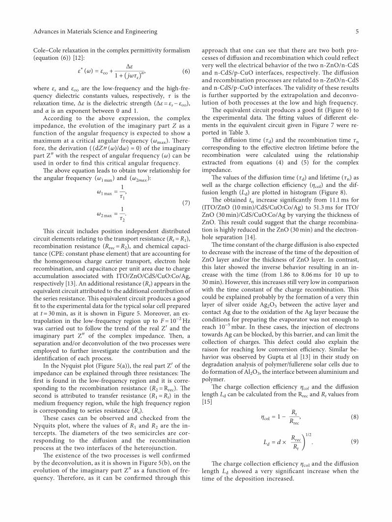
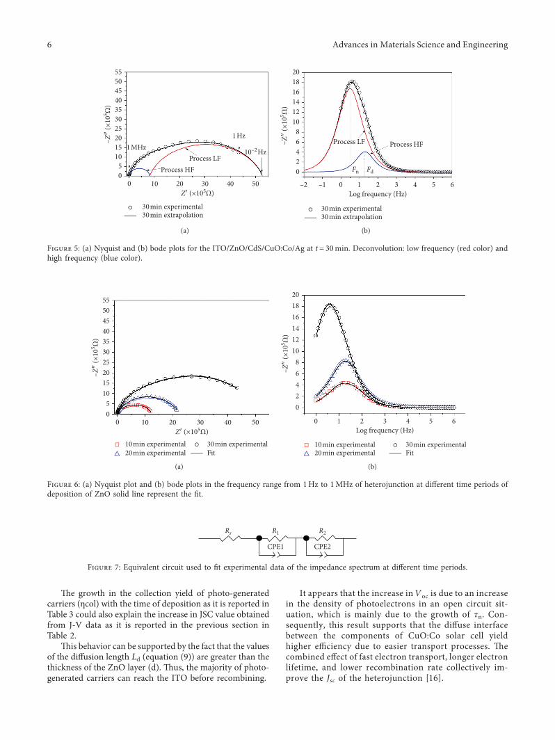
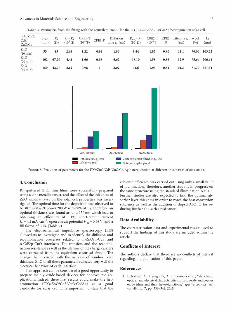
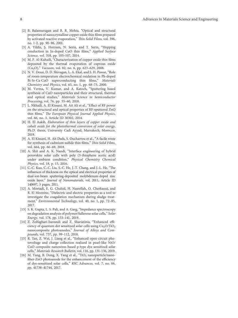


![Synthesis and Characterisation of Lanthanum added ZnO ...joics.org/gallery/ics-1925.pdf · ZnO [26-30]. It clearly shows that the prepared ZnO and La doped ZnO samples revelation](https://img.pdfslide.net/doc/110x75/5ea23502b68dcf2dd872f588/synthesis-and-characterisation-of-lanthanum-added-zno-joicsorggalleryics-1925pdf.jpg)