Embed Size (px)
Citation preview
1
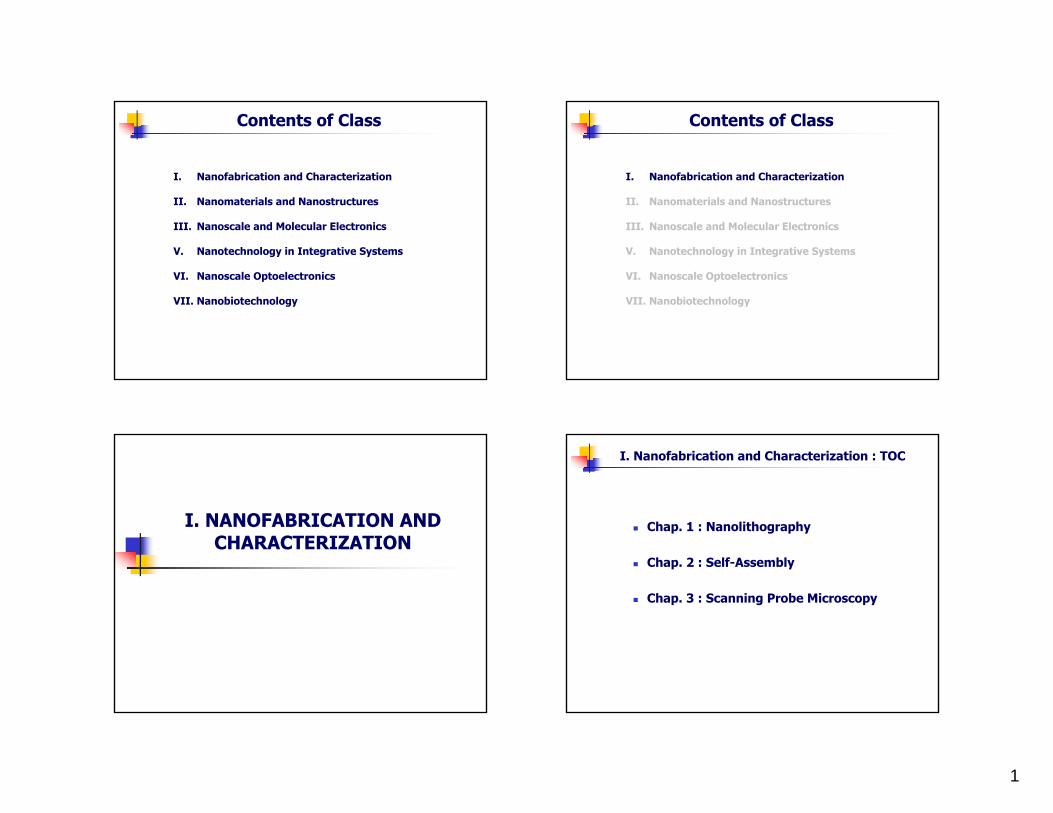
Contents of Class
I. Nanofabrication and Characterization
II. Nanomaterials and Nanostructures
III. Nanoscale and Molecular Electronics
V. Nanotechnology in Integrative Systems
VI. Nanoscale Optoelectronics
VII. Nanobiotechnology
Contents of Class
I. Nanofabrication and Characterization
II. Nanomaterials and Nanostructures
III. Nanoscale and Molecular Electronics
V. Nanotechnology in Integrative Systems
VI. Nanoscale Optoelectronics
VII. Nanobiotechnology
I. NANOFABRICATION AND CHARACTERIZATION
I. Nanofabrication and Characterization : TOC
Chap. 1 : Nanolithography
Chap. 2 : Self-Assembly
Chap. 3 : Scanning Probe Microscopy
2
I. Nanofabrication and Characterization : TOC
Chap. 1 : Nanolithography
Chap. 2 : Self-Assembly
Chap. 3 : Scanning Probe Microscopy
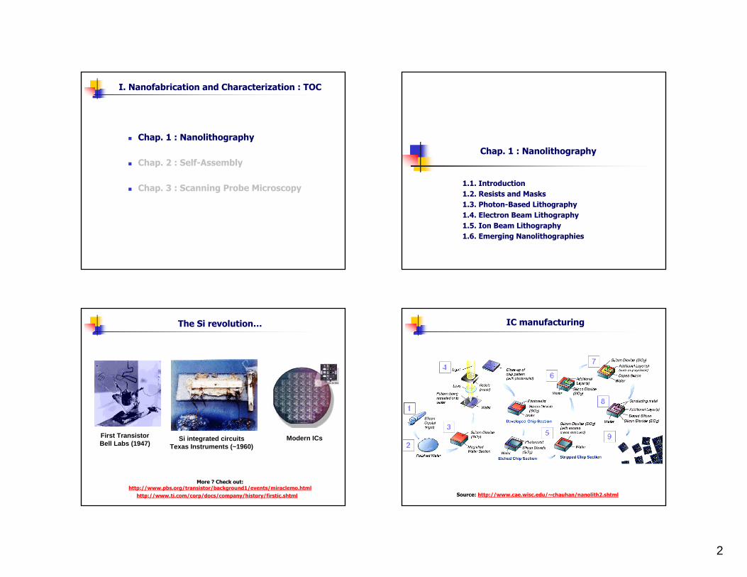
Chap. 1 : Nanolithography
1.1. Introduction1.2. Resists and Masks1.3. Photon-Based Lithography1.4. Electron Beam Lithography1.5. Ion Beam Lithography1.6. Emerging Nanolithographies
The Si revolution…
First TransistorBell Labs (1947)
Si integrated circuitsTexas Instruments (~1960)
Modern ICs
More ? Check out:http://www.pbs.org/transistor/background1/events/miraclemo.html
http://www.ti.com/corp/docs/company/history/firstic.shtml
IC manufacturing
Source: http://www.cae.wisc.edu/~chauhan/nanolith2.shtml

3
The need of micropatterning
The batch fabrication of microstructures requires a low-cost, high throughput surface patterning technology
Overview of photolithography
Overview of photolithography (ctnd.)
Lithography consists of patterning substrate by employing the interaction of beams of photons or particles with materials.
Photolithography is widely used in the integrated circuits (ICs) manufacturing.
The process of IC manufacturing consists of a series of 10-20 steps or more, called mask layerswhere layers of materials coated with resists are patterned then transferred onto the material layer.
Overview of photolithography (ctnd.)
A photolithography system consists of a light source, a mask, and a optical projection system.
Photoresists are radiation sensitive materials that usually consist of a photo-sensitive compound, a polymeric backbone, and a solvent.
Resists can be classified upon their solubility after exposure into: positive resists (solubility of exposed area increases) and negative resists(solubility of exposed area decreases).

4
Chap. 1 : Nanolithography
1.1. Introduction1.2. Resists and Masks1.3. Photon-Based Lithography1.4. Electron Beam Lithography1.5. Ion Beam Lithography1.6. Emerging Nanolithographies
Positive vs. negative photoresists
Threshold and clearing doses
Solubility vs exposure dose of a positive photoresist
“contrast” γ of resist :
⎥⎦
⎤⎢⎣
⎡=γ
0
c
DDlog
1
⎟⎟⎠
⎞⎜⎜⎝
⎛⋅γ−=
CDDoselogremainingfraction
Threshold and clearing doses: example
Question:A positive photoresist possesses a contrast γ = 5, and a clearing doseDc = 300 mJ/cm2. What dose is required to dissolve 50 % of the resist thickness ?
Answer: The resist will have a threshold dose Do:
γ−
⋅=1
C0 10DD
51
10300−
⋅=
2cm/mJ189=
The contrast curve is analytically given by:
2cm/mJ237Dose =
⎟⎟⎠
⎞⎜⎜⎝
⎛⋅γ−=
CDDoselogremainingfraction
⎟⎠⎞
⎜⎝⎛⋅−=
300Doselog55.0
The resist will be 50 % dissolved when using a dose of 237 mJ/cm2

5
Types of photolithography
Contact Printing Proximity Printing Projection Printing
Resolution of photolithography
gWmin λ=
Contact lithography limited by Fresnel diffraction:
where λ is wavelength employed and g is mask-resist gap.
Projection lithography limited by Rayleigh's criterion:
where λ is wavelength employed, NA is numerical aperture of lense(NA = sin α), and k1 is a constant (typically k1 = 0.6 - 0.8)
NAkR 1λ=
Resolution of photolithography: exampleQuestion:An x-ray contact lithography system uses photons of energy of 1 keV. If the separation between the mask and the wafer is 20 μm, estimate the diffraction-limited resolution that is achievable by this system
Answer:The energy Ep of photons is related to their wavelength λ through:
where h = 6.626× 10⁻³⁴ m2 kg/s is Planck’s constant, and c = 3 x 10⁸ m/s is the speed of light.
Thus, the wavelength of the photons employed is:
λ=
hcEp
19
834
10x6.1100010x310x626.6
−
−
⋅⋅
=λ
nm24.1=λ
The minimum feature size that can be resolved is:
gWmin λ=69
min 10x2010x24.1W −− ⋅=
nm157Wmin =
Resolution of photolithography (ctnd.)

6
Chap. 1 : Nanolithography
1.1. Introduction1.2. Resists and Masks1.3. Photon-Based Lithography1.4. Electron Beam Lithography1.5. Ion Beam Lithography1.6. Emerging Nanolithographies
Diffraction and other optical effects likely to limit the resolution of “standard” DUV (λ = 193 nm) lithography to the 75-100 nm range.
Upcoming generation (2005) to employ DUV (λ = 193 nm) based 65 nm lithography and 35 nm gate lengths.
Intel lithography roadmap will eventually skip λ = 157 nm technology and pursue well into the sub-100 nm region through EUV (λ = 13.5 nm) (~2009)
Exploratory research in the sub-100 nm region may also be accomplished through alternate patterning techniques such as x-ray-, ion- and electron beam- lithography.
Micro- and nanolithography
Intel lithography roadmap (Nov 2004) EUV lithography system
EUV Systems to employ reflective instead of refractive optics

7
EUV lithography system (ctnd.) EUV lithography system (ctnd.)
50 nm lines fabricated with EUV lithography (~1999)30 nm features now routinely achieved
EUV lithography system (ctnd.)
One in every home...
X-Ray lithography
Diffraction limits lithography resolution to λ/2Obvious solution: use lower wavelengths sourcesDUV and EUV approaching standardizationX-Ray lithography still at “exploratory” stage

8
Plasma X-Ray source Structures produced with X-ray litho. (ctnd.)
125 nm feature exposed with SAL
Source: SAL, Inc.
Chap. 1 : Nanolithography
1.1. Introduction1.2. Resists and Masks1.3. Photon-Based Lithography1.4. Electron Beam Lithography1.5. Ion Beam Lithography1.6. Emerging Nanolithographies
1) Casting of thin PMMA film
2) E-beam patterning of PMMA
e
3) Development of PMMA
4) Metallization
5) Lift-offEmploys a beam of electron instead of photons
Advantage: Fast turn-around timeDisadvantage: Slow throughput
Electron beam lithography
More ? Google it ! Also, check out R.F.W. Pease, Stanford

9
Throughput enhanced by variable beam shaping
Electron beam lithography system Applications of electron beam lithography
Mainly employed for the fabrication of photomasks
Also used to write patterns directly on wafer
Scattering phenomena in e-beam litho
Scattering phenomena dictate resolutionBetter resolution achieved at higher beam energies
E-beam fabricated nanostructures
30 nm thick poly(methyl methacrylate) (PMMA) is spin-cast on Si substrate.Exposure to e-beam along vertical lines spaced 50 nm apart, breaks polymer bonds and increases solubility.10 nm lines are dissolved away by a solvent.

10
Electron beam projection lithography (EPL)
SCALPEL System (Lucent Technologies)
Electron beam projection lithography (ctnd.)
Principle of continuous membrane EPL
Structures produced by EPL
Technology was a serious contender for future sub-70 nm nodes
Relatively low throughput and high cost of mask precluded its viability
Eventually abandoned (~2001) in favor of EUV (λ = 13.5 nm) optical systems
Chap. 1 : Nanolithography
1.1. Introduction1.2. Resists and Masks1.3. Photon-Based Lithography1.4. Electron Beam Lithography1.5. Ion Beam Lithography1.6. Emerging Nanolithographies

11
Ion beam lithography
Advantages of ion beams:Enhanced resists sensitivity Can be focused to narrower linewidthReduced scatteringAllows hybrid processes such as ion-induced etching and implantation
1) Casting of thin resist film 2) Ion beam patterning of resist
i
3) Development of resist
More ? Google it !
Focused ion beam lithography
FIBL components:Ion sourceIon optics columnSample displacement table
Specifications:Accelerating voltage 3-200 kV.Current density up to 10 A/cm2 .Beam diameter 0.5-1.0 μm.Ions: Ga+ , Au+ ,Si+ ,Be+ etc.
Provides sub-micrometer beam with good current density (1-5 A/cm2 ) for metals with a relatively low melting temp and vapor pressure (ie. Ga, In, Sn etc).
Liquid metal ion sources FIB fabricated nanostructures

12
Effects of the ion beam on the substrate:
Displacement of atoms.Emission of electrons.Chemical effect like change of solubility of the resist.Sputtering of substrate atoms by low energy ions.
May result in resist heating as high as 1500o C
Issues in FIBL
Chap. 1 : Nanolithography
1.1. Introduction1.2. Resists and Masks1.3. Photon-Based Lithography1.4. Electron Beam Lithography1.5. Ion Beam Lithography1.6. Emerging Nanolithographies
Alternate Nanolithography Techniques
Micro-contact Printing
Nanoimprint Lithography
Scanned Probe Lithography
Dip-pen Lithography
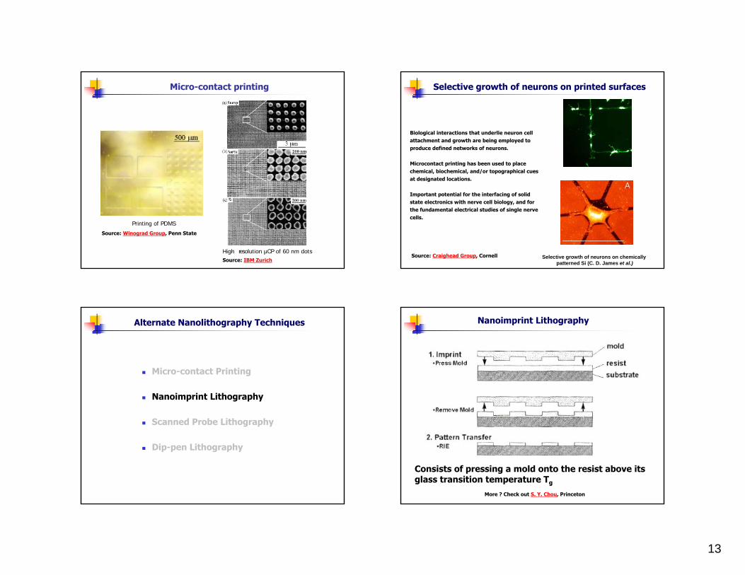
Micro-contact printing
1) Application of ink to stamp 2) Application of stamp to surface
3) Removal of stamp 4) Residues rinsed off
Source: IBM Zurich
13
Micro-contact printing
High- resolution µCP of 60 nm dots Source: IBM Zurich
Printing of PDMS
Source: Winograd Group, Penn State
Biological interactions that underlie neuron cell attachment and growth are being employed to produce defined networks of neurons.
Microcontact printing has been used to place chemical, biochemical, and/or topographical cues at designated locations.
Important potential for the interfacing of solid state electronics with nerve cell biology, and for the fundamental electrical studies of single nerve cells.
Selective growth of neurons on chemically patterned Si (C. D. James et al.)
Selective growth of neurons on printed surfaces
Source: Craighead Group, Cornell
Alternate Nanolithography Techniques
Micro-contact Printing
Nanoimprint Lithography
Scanned Probe Lithography
Dip-pen Lithography
Nanoimprint Lithography
Consists of pressing a mold onto the resist above its glass transition temperature Tg
More ? Check out S. Y. Chou, Princeton

14
NIL master
SiO2 pillars with 10 nm diameter, 40 nm spacing, and 60 nm height fabricated by e-beam lithography.
Master can be used tens of times without degradation
NIL pattern in PMMA
Mask is pressed into 80 nm thick layer of PMMA on Si substrate at 175° C (Tg=105 ° C), P= 4.4 MPa.
PMMA conforms to master patterng, resulting in ~10 nm range holes
Metal dots by NIL
Reactive ion etching is used to cut down resist thickness until shallow regions are completely removed
Ti/Au is deposited onto resist.
Resist and metal-coating is removed by solvent leaving behind metal dots where resist had been removed.
Alternate Nanolithography Techniques
Micro-contact Printing
Nanoimprint Lithography
Scanned Probe Lithography
Dip-pen Lithography

15
Source: Quate Group, Stanford
Scanned Probe Lithography Fabrication of CMOS gate using SPM lithography
Source: Quate Group, Stanford
Alternate Nanolithography Techniques
Micro-contact Printing
Nanoimprint Lithography
Scanned Probe Lithography
Dip-pen Lithography
Dip-pen lithography
Source: Mirkin Group, NWU

16
Dip-pen lithography
Source: Mirkin Group, NWU
A) Ultra-high resolution pattern of mercaptohexadecanoic acid on atomically-flat gold surface. B) DPN generated multi-component nanostructure with two aligned alkanethiol patterns. C) Richard Feynmann's historic speech written using the DPN nanoplotter