Embed Size (px)
Citation preview
This article has been accepted for inclusion in a future issue of this journal. Content is final as presented, with the exception of pagination.
IEEE TRANSACTIONS ON BIOMEDICAL CIRCUITS AND SYSTEMS 1
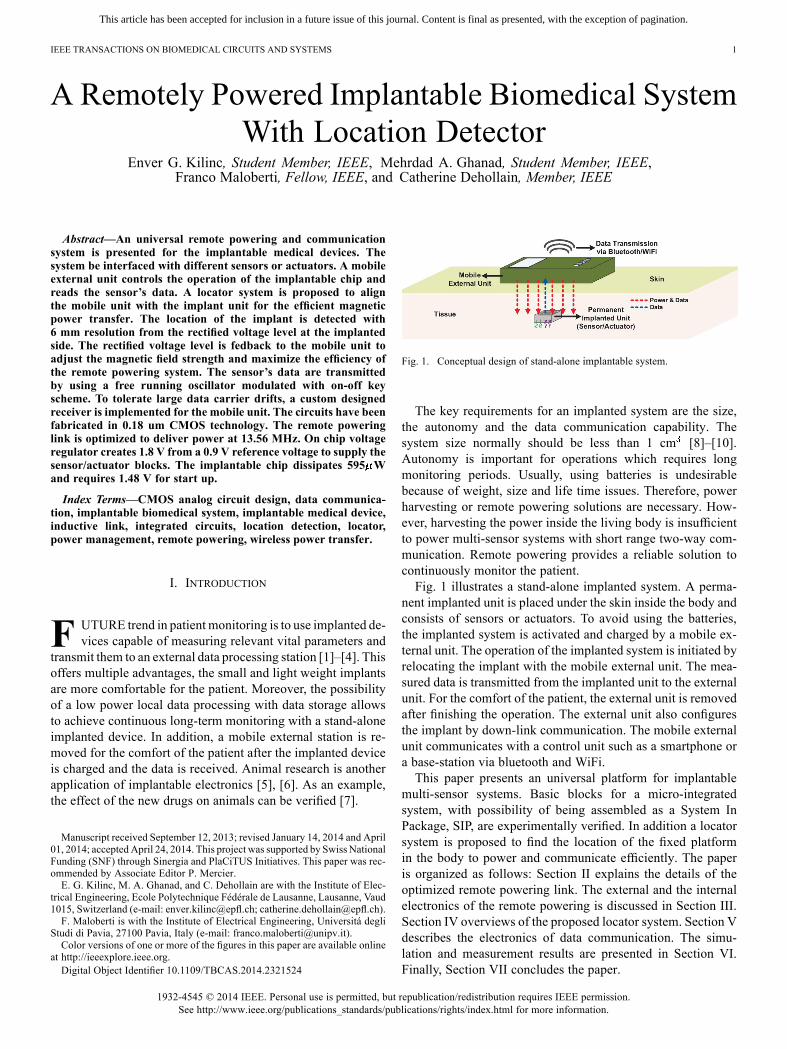
A Remotely Powered Implantable Biomedical SystemWith Location Detector
Enver G. Kilinc, Student Member, IEEE, Mehrdad A. Ghanad, Student Member, IEEE,Franco Maloberti, Fellow, IEEE, and Catherine Dehollain, Member, IEEE
Abstract—An universal remote powering and communicationsystem is presented for the implantable medical devices. Thesystem be interfaced with different sensors or actuators. A mobileexternal unit controls the operation of the implantable chip andreads the sensor’s data. A locator system is proposed to alignthe mobile unit with the implant unit for the efficient magneticpower transfer. The location of the implant is detected with6 mm resolution from the rectified voltage level at the implantedside. The rectified voltage level is fedback to the mobile unit toadjust the magnetic field strength and maximize the efficiency ofthe remote powering system. The sensor’s data are transmittedby using a free running oscillator modulated with on-off keyscheme. To tolerate large data carrier drifts, a custom designedreceiver is implemented for the mobile unit. The circuits have beenfabricated in 0.18 um CMOS technology. The remote poweringlink is optimized to deliver power at 13.56 MHz. On chip voltageregulator creates 1.8 V from a 0.9 V reference voltage to supply thesensor/actuator blocks. The implantable chip dissipates 595 Wand requires 1.48 V for start up.
Index Terms—CMOS analog circuit design, data communica-tion, implantable biomedical system, implantable medical device,inductive link, integrated circuits, location detection, locator,power management, remote powering, wireless power transfer.
I. INTRODUCTION
F UTURE trend in patient monitoring is to use implanted de-vices capable of measuring relevant vital parameters and
transmit them to an external data processing station [1]–[4]. Thisoffers multiple advantages, the small and light weight implantsare more comfortable for the patient. Moreover, the possibilityof a low power local data processing with data storage allowsto achieve continuous long-term monitoring with a stand-aloneimplanted device. In addition, a mobile external station is re-moved for the comfort of the patient after the implanted deviceis charged and the data is received. Animal research is anotherapplication of implantable electronics [5], [6]. As an example,the effect of the new drugs on animals can be verified [7].
Manuscript received September 12, 2013; revised January 14, 2014 and April01, 2014; accepted April 24, 2014. This project was supported by Swiss NationalFunding (SNF) through Sinergia and PlaCiTUS Initiatives. This paper was rec-ommended by Associate Editor P. Mercier.E. G. Kilinc, M. A. Ghanad, and C. Dehollain are with the Institute of Elec-
trical Engineering, Ecole Polytechnique Fédérale de Lausanne, Lausanne, Vaud1015, Switzerland (e-mail: [email protected]; [email protected]).F. Maloberti is with the Institute of Electrical Engineering, Universitá degli
Studi di Pavia, 27100 Pavia, Italy (e-mail: [email protected]).Color versions of one or more of the figures in this paper are available online
at http://ieeexplore.ieee.org.Digital Object Identifier 10.1109/TBCAS.2014.2321524
Fig. 1. Conceptual design of stand-alone implantable system.
The key requirements for an implanted system are the size,the autonomy and the data communication capability. Thesystem size normally should be less than 1 cm [8]–[10].Autonomy is important for operations which requires longmonitoring periods. Usually, using batteries is undesirablebecause of weight, size and life time issues. Therefore, powerharvesting or remote powering solutions are necessary. How-ever, harvesting the power inside the living body is insufficientto power multi-sensor systems with short range two-way com-munication. Remote powering provides a reliable solution tocontinuously monitor the patient.Fig. 1 illustrates a stand-alone implanted system. A perma-
nent implanted unit is placed under the skin inside the body andconsists of sensors or actuators. To avoid using the batteries,the implanted system is activated and charged by a mobile ex-ternal unit. The operation of the implanted system is initiated byrelocating the implant with the mobile external unit. The mea-sured data is transmitted from the implanted unit to the externalunit. For the comfort of the patient, the external unit is removedafter finishing the operation. The external unit also configuresthe implant by down-link communication. The mobile externalunit communicates with a control unit such as a smartphone ora base-station via bluetooth and WiFi.This paper presents an universal platform for implantable
multi-sensor systems. Basic blocks for a micro-integratedsystem, with possibility of being assembled as a System InPackage, SIP, are experimentally verified. In addition a locatorsystem is proposed to find the location of the fixed platformin the body to power and communicate efficiently. The paperis organized as follows: Section II explains the details of theoptimized remote powering link. The external and the internalelectronics of the remote powering is discussed in Section III.Section IV overviews of the proposed locator system. Section Vdescribes the electronics of data communication. The simu-lation and measurement results are presented in Section VI.Finally, Section VII concludes the paper.
1932-4545 © 2014 IEEE. Personal use is permitted, but republication/redistribution requires IEEE permission.See http://www.ieee.org/publications_standards/publications/rights/index.html for more information.
This article has been accepted for inclusion in a future issue of this journal. Content is final as presented, with the exception of pagination.
2 IEEE TRANSACTIONS ON BIOMEDICAL CIRCUITS AND SYSTEMS
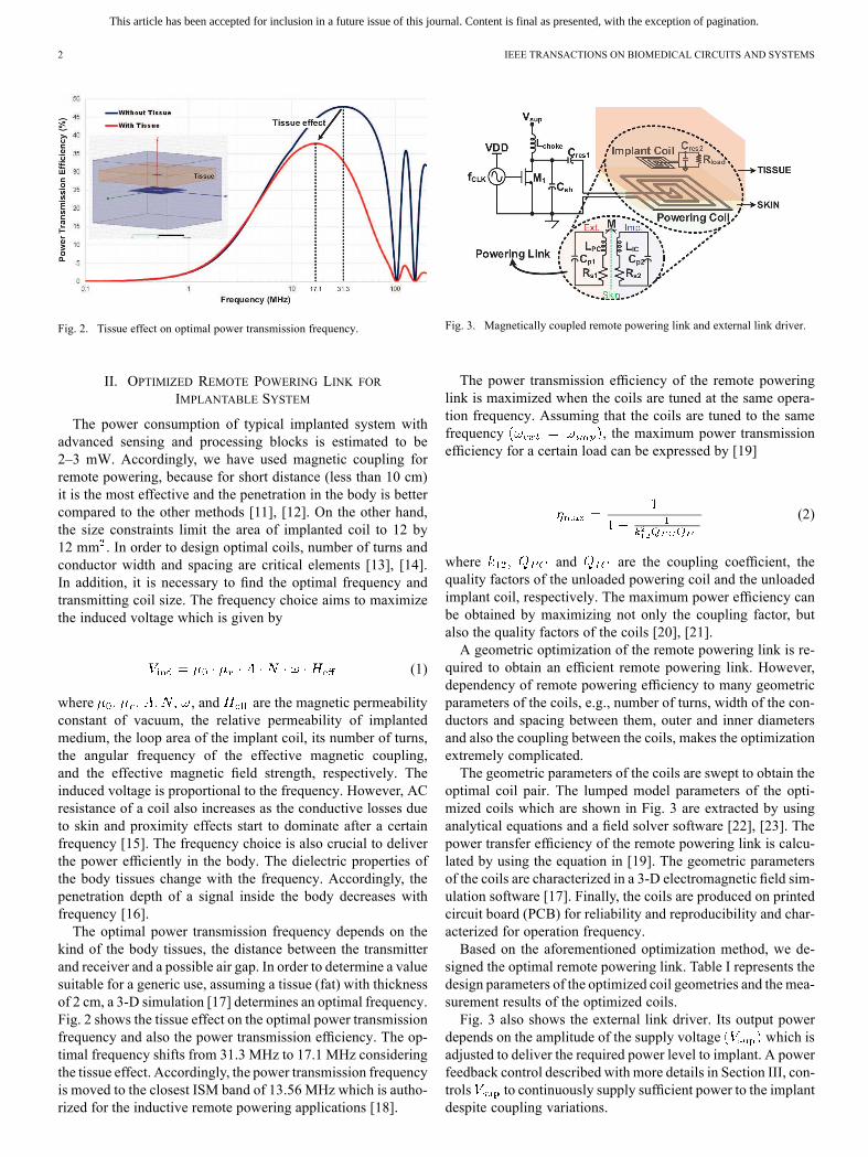
Fig. 2. Tissue effect on optimal power transmission frequency.
II. OPTIMIZED REMOTE POWERING LINK FOR
IMPLANTABLE SYSTEM
The power consumption of typical implanted system withadvanced sensing and processing blocks is estimated to be2–3 mW. Accordingly, we have used magnetic coupling forremote powering, because for short distance (less than 10 cm)it is the most effective and the penetration in the body is bettercompared to the other methods [11], [12]. On the other hand,the size constraints limit the area of implanted coil to 12 by12 mm . In order to design optimal coils, number of turns andconductor width and spacing are critical elements [13], [14].In addition, it is necessary to find the optimal frequency andtransmitting coil size. The frequency choice aims to maximizethe induced voltage which is given by
(1)
where , and are the magnetic permeabilityconstant of vacuum, the relative permeability of implantedmedium, the loop area of the implant coil, its number of turns,the angular frequency of the effective magnetic coupling,and the effective magnetic field strength, respectively. Theinduced voltage is proportional to the frequency. However, ACresistance of a coil also increases as the conductive losses dueto skin and proximity effects start to dominate after a certainfrequency [15]. The frequency choice is also crucial to deliverthe power efficiently in the body. The dielectric properties ofthe body tissues change with the frequency. Accordingly, thepenetration depth of a signal inside the body decreases withfrequency [16].The optimal power transmission frequency depends on the
kind of the body tissues, the distance between the transmitterand receiver and a possible air gap. In order to determine a valuesuitable for a generic use, assuming a tissue (fat) with thicknessof 2 cm, a 3-D simulation [17] determines an optimal frequency.Fig. 2 shows the tissue effect on the optimal power transmissionfrequency and also the power transmission efficiency. The op-timal frequency shifts from 31.3 MHz to 17.1 MHz consideringthe tissue effect. Accordingly, the power transmission frequencyis moved to the closest ISM band of 13.56 MHz which is autho-rized for the inductive remote powering applications [18].
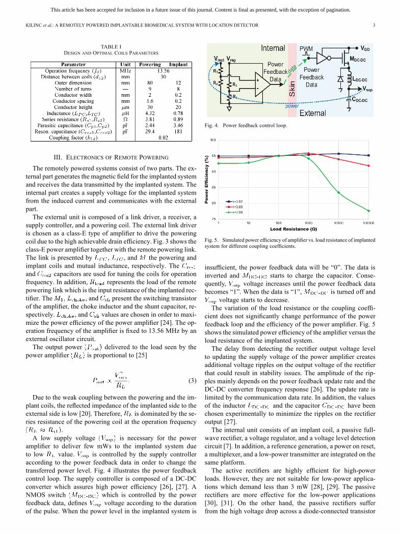
Fig. 3. Magnetically coupled remote powering link and external link driver.
The power transmission efficiency of the remote poweringlink is maximized when the coils are tuned at the same opera-tion frequency. Assuming that the coils are tuned to the samefrequency , the maximum power transmissionefficiency for a certain load can be expressed by [19]
(2)
where and are the coupling coefficient, thequality factors of the unloaded powering coil and the unloadedimplant coil, respectively. The maximum power efficiency canbe obtained by maximizing not only the coupling factor, butalso the quality factors of the coils [20], [21].A geometric optimization of the remote powering link is re-
quired to obtain an efficient remote powering link. However,dependency of remote powering efficiency to many geometricparameters of the coils, e.g., number of turns, width of the con-ductors and spacing between them, outer and inner diametersand also the coupling between the coils, makes the optimizationextremely complicated.The geometric parameters of the coils are swept to obtain the
optimal coil pair. The lumped model parameters of the opti-mized coils which are shown in Fig. 3 are extracted by usinganalytical equations and a field solver software [22], [23]. Thepower transfer efficiency of the remote powering link is calcu-lated by using the equation in [19]. The geometric parametersof the coils are characterized in a 3-D electromagnetic field sim-ulation software [17]. Finally, the coils are produced on printedcircuit board (PCB) for reliability and reproducibility and char-acterized for operation frequency.Based on the aforementioned optimization method, we de-
signed the optimal remote powering link. Table I represents thedesign parameters of the optimized coil geometries and the mea-surement results of the optimized coils.Fig. 3 also shows the external link driver. Its output power
depends on the amplitude of the supply voltage which isadjusted to deliver the required power level to implant. A powerfeedback control described with more details in Section III, con-trols to continuously supply sufficient power to the implantdespite coupling variations.
This article has been accepted for inclusion in a future issue of this journal. Content is final as presented, with the exception of pagination.
KILINC et al.: A REMOTELY POWERED IMPLANTABLE BIOMEDICAL SYSTEM WITH LOCATION DETECTOR 3
TABLE IDESIGN AND OPTIMAL COILS PARAMETERS
III. ELECTRONICS OF REMOTE POWERING
The remotely powered systems consist of two parts. The ex-ternal part generates the magnetic field for the implanted systemand receives the data transmitted by the implanted system. Theinternal part creates a supply voltage for the implanted systemfrom the induced current and communicates with the externalpart.The external unit is composed of a link driver, a receiver, a
supply controller, and a powering coil. The external link driveris chosen as a class-E type of amplifier to drive the poweringcoil due to the high achievable drain efficiency. Fig. 3 shows theclass-E power amplifier together with the remote powering link.The link is presented by , and the powering andimplant coils and mutual inductance, respectively. Theand capacitors are used for tuning the coils for operationfrequency. In addition, represents the load of the remotepowering link which is the input resistance of the implanted rec-tifier. The , and present the switching transistorof the amplifier, the choke inductor and the shunt capacitor, re-spectively. , and values are chosen in order to maxi-mize the power efficiency of the power amplifier [24]. The op-eration frequency of the amplifier is fixed to 13.56 MHz by anexternal oscillator circuit.The output power delivered to the load seen by the
power amplifier is proportional to [25]
(3)
Due to the weak coupling between the powering and the im-plant coils, the reflected impedance of the implanted side to theexternal side is low [20]. Therefore, is dominated by the se-ries resistance of the powering coil at the operation frequency
.A low supply voltage is necessary for the power
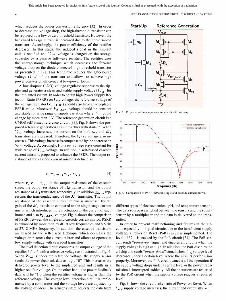
amplifier to deliver few mWs to the implanted system dueto low value. is controlled by the supply controlleraccording to the power feedback data in order to change thetransferred power level. Fig. 4 illustrates the power feedbackcontrol loop. The supply controller is composed of a DC-DCconverter which assures high power efficiency [26], [27]. ANMOS switch - which is controlled by the powerfeedback data, defines voltage according to the durationof the pulse. When the power level in the implanted system is
Fig. 4. Power feedback control loop.
Fig. 5. Simulated power efficiency of amplifier vs. load resistance of implantedsystem for different coupling coefficients.
insufficient, the power feedback data will be “0”. The data isinverted and - starts to charge the capacitor. Conse-quently, voltage increases until the power feedback databecomes “1”. When the data is “1”, - is turned off and
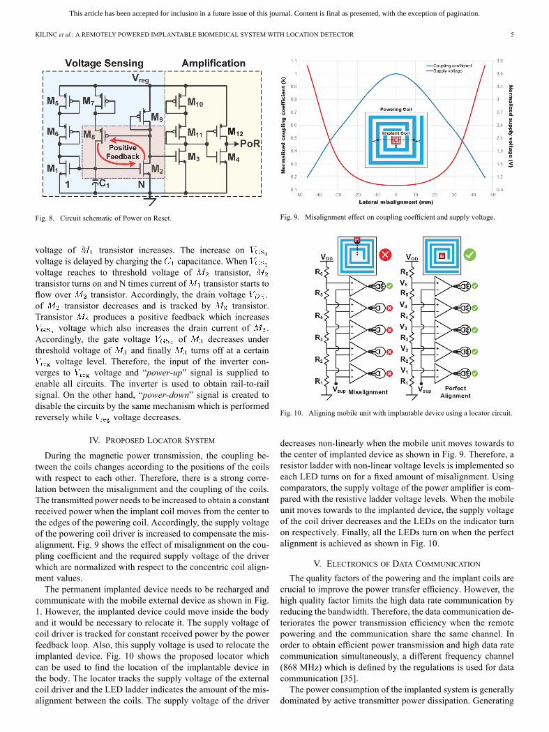
voltage starts to decrease.The variation of the load resistance or the coupling coeffi-
cient does not significantly change performance of the powerfeedback loop and the efficiency of the power amplifier. Fig. 5shows the simulated power efficiency of the amplifier versus theload resistance of the implanted system.The delay from detecting the rectifier output voltage level
to updating the supply voltage of the power amplifier createsadditional voltage ripples on the output voltage of the rectifierthat could result in stability issues. The amplitude of the rip-ples mainly depends on the power feedback update rate and theDC-DC converter frequency response [26]. The update rate islimited by the communication data rate. In addition, the valuesof the inductor - and the capacitor - have beenchosen experimentally to minimize the ripples on the rectifieroutput [27].The internal unit consists of an implant coil, a passive full-
wave rectifier, a voltage regulator, and a voltage level detectioncircuit [7]. In addition, a reference generation, a power on reset,a multiplexer, and a low-power transmitter are integrated on thesame platform.The active rectifiers are highly efficient for high-power
loads. However, they are not suitable for low-power applica-tions which demand less than 3 mW [28], [29]. The passiverectifiers are more effective for the low-power applications[30], [31]. On the other hand, the passive rectifiers sufferfrom the high voltage drop across a diode-connected transistor
This article has been accepted for inclusion in a future issue of this journal. Content is final as presented, with the exception of pagination.
4 IEEE TRANSACTIONS ON BIOMEDICAL CIRCUITS AND SYSTEMS
which reduces the power conversion efficiency [32]. In orderto decrease the voltage drop, the high-threshold transistor canbe replaced by a low or zero threshold transistor. However, thebackward leakage current is increased due to the non-disabledtransistor. Accordingly, the power efficiency of the rectifierdecreases. In this study, the induced signal in the implantcoil is rectified and voltage is charged on the storagecapacitor by a passive full-wave rectifier. The rectifier usesthe charge-storage technique which decreases the forwardvoltage drop on the diode connected high-threshold transistoras presented in [7]. This technique reduces the gate-sourcevoltage of the transistor and allows to achieve highpower conversion efficiency at low-power loads.A low-dropout (LDO) voltage regulator suppresses the rip-
ples and generates a clean and stable supply voltage forthe implanted system. In order to obtain high Power Supply Re-jection Ratio (PSRR) on voltage, the reference voltage ofthe voltage regulator should also have an acceptablePSRR value. Moreover, voltage should be constantand stable for wide range of supply variation where couldchange by more than 1 V. The reference generation circuit is aCMOS self-biased reference circuit [33]. Fig. 6 shows the pro-posed reference generation circuit together with start-up. When
voltage increases, the current on the both andtransistors are increased. Therefore, the voltage also in-creases. This voltage increase is compensated by the decrease on
voltage. Accordingly, voltage stays constant forwide range of voltage. In addition, a self-biased cascodecurrent mirror is proposed to enhance the PSRR. The output re-sistance of the cascode current mirror is defined as
(4)
where is the output resistance of the cascodestage, the output resistance of transistor, and the outputresistance of transistor, respectively. In addition, rep-resents the transconductance of the transistor. The outputresistance of the cascode current mirror is increased by thegain of the transistor compared to the single stage currentmirror which introduces more fluctuation on the current of eachbranch and also voltage. Fig. 6 shows the comparisonof PSRR between the single and cascode current mirror. PSRRis enhanced by more than 25 dB at low frequencies and 5.5 dBat 27.12 MHz frequency. In addition, the cascode transistorsare biased by the self-biased technique which decreases thevoltage drop across the current mirror and allows to operate atlow supply voltage with cascaded transistors.The level detection circuit compares the output voltage of the
rectifier with a reference voltage as illustrated in Fig. 4.When is under the reference voltage, the supply sensorsends the power feedback data as logic “0”. This increases thedelivered power level to the implanted unit and results in ahigher rectifier voltage. On the other hand, the power feedbackdata will be “1”, when the rectifier voltage is higher than thereference voltage. The voltage level detection circuit is imple-mented by a comparator and the voltage levels are adjusted bythe voltage dividers. The sensor system collects the data from
Fig. 6. Proposed reference generation circuit with start-up.
Fig. 7. Comparison of PSRR between single and cascode current mirror.
different types of electrochemical, pH, and temperature sensors.The data source is switched between the sensors and the supplysensor by a multiplexer and the data is delivered to the trans-mitter.In order to prevent malfunctioning and failures in the cir-
cuits especially in digital circuits due to the insufficient supplyvoltage, a Power on Reset (PoR) circuit is implemented. Thelevel of is tracked by the PoR circuit [34]. The PoR cir-cuit sends “power-up” signal and enables all circuits when thesupply voltage is high enough. In addition, the PoR disables theall chip and sends “power-down” signal when voltage leveldecreases under a certain level where the circuits perform im-properly. Moreover, the PoR circuit cancels all the operation ifthe supply voltage drops under a certain level or the power trans-mission is interrupted suddenly. All the operations are restartedby the PoR circuit when the supply voltage reaches a requiredlevel.Fig. 8 shows the circuit schematic of Power on Reset. Whensupply voltage increases, the current and eventually
This article has been accepted for inclusion in a future issue of this journal. Content is final as presented, with the exception of pagination.
KILINC et al.: A REMOTELY POWERED IMPLANTABLE BIOMEDICAL SYSTEM WITH LOCATION DETECTOR 5
Fig. 8. Circuit schematic of Power on Reset.
voltage of transistor increases. The increase onvoltage is delayed by charging the capacitance. Whenvoltage reaches to threshold voltage of transistor,transistor turns on and N times current of transistor starts toflow over transistor. Accordingly, the drain voltageof transistor decreases and is tracked by transistor.Transistor produces a positive feedback which increases
voltage which also increases the drain current of .Accordingly, the gate voltage of decreases underthreshold voltage of and finally turns off at a certain
voltage level. Therefore, the input of the inverter con-verges to voltage and “power-up” signal is supplied toenable all circuits. The inverter is used to obtain rail-to-railsignal. On the other hand, “power-down” signal is created todisable the circuits by the same mechanism which is performedreversely while voltage decreases.
IV. PROPOSED LOCATOR SYSTEM
During the magnetic power transmission, the coupling be-tween the coils changes according to the positions of the coilswith respect to each other. Therefore, there is a strong corre-lation between the misalignment and the coupling of the coils.The transmitted power needs to be increased to obtain a constantreceived power when the implant coil moves from the center tothe edges of the powering coil. Accordingly, the supply voltageof the powering coil driver is increased to compensate the mis-alignment. Fig. 9 shows the effect of misalignment on the cou-pling coefficient and the required supply voltage of the driverwhich are normalized with respect to the concentric coil align-ment values.The permanent implanted device needs to be recharged and
communicate with the mobile external device as shown in Fig.1. However, the implanted device could move inside the bodyand it would be necessary to relocate it. The supply voltage ofcoil driver is tracked for constant received power by the powerfeedback loop. Also, this supply voltage is used to relocate theimplanted device. Fig. 10 shows the proposed locator whichcan be used to find the location of the implantable device inthe body. The locator tracks the supply voltage of the externalcoil driver and the LED ladder indicates the amount of the mis-alignment between the coils. The supply voltage of the driver
Fig. 9. Misalignment effect on coupling coefficient and supply voltage.
Fig. 10. Aligning mobile unit with implantable device using a locator circuit.
decreases non-linearly when the mobile unit moves towards tothe center of implanted device as shown in Fig. 9. Therefore, aresistor ladder with non-linear voltage levels is implemented soeach LED turns on for a fixed amount of misalignment. Usingcomparators, the supply voltage of the power amplifier is com-pared with the resistive ladder voltage levels. When the mobileunit moves towards to the implanted device, the supply voltageof the coil driver decreases and the LEDs on the indicator turnon respectively. Finally, all the LEDs turn on when the perfectalignment is achieved as shown in Fig. 10.
V. ELECTRONICS OF DATA COMMUNICATION
The quality factors of the powering and the implant coils arecrucial to improve the power transfer efficiency. However, thehigh quality factor limits the high data rate communication byreducing the bandwidth. Therefore, the data communication de-teriorates the power transmission efficiency when the remotepowering and the communication share the same channel. Inorder to obtain efficient power transmission and high data ratecommunication simultaneously, a different frequency channel(868 MHz) which is defined by the regulations is used for datacommunication [35].The power consumption of the implanted system is generally
dominated by active transmitter power dissipation. Generating
This article has been accepted for inclusion in a future issue of this journal. Content is final as presented, with the exception of pagination.
6 IEEE TRANSACTIONS ON BIOMEDICAL CIRCUITS AND SYSTEMS
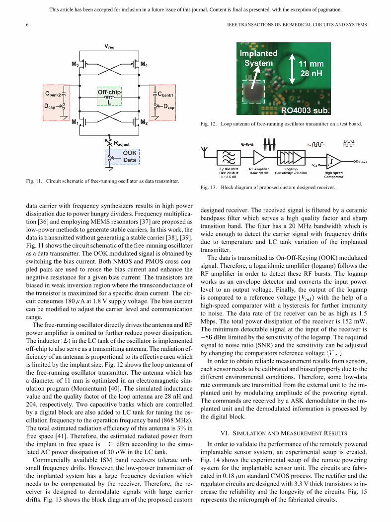
Fig. 11. Circuit schematic of free-running oscillator as data transmitter.
data carrier with frequency synthesizers results in high powerdissipation due to power hungry dividers. Frequencymultiplica-tion [36] and employing MEMS resonators [37] are proposed aslow-power methods to generate stable carriers. In this work, thedata is transmitted without generating a stable carrier [38], [39].Fig. 11 shows the circuit schematic of the free-running oscillatoras a data transmitter. The OOK modulated signal is obtained byswitching the bias current. Both NMOS and PMOS cross-cou-pled pairs are used to reuse the bias current and enhance thenegative resistance for a given bias current. The transistors arebiased in weak inversion region where the transconductance ofthe transistor is maximized for a specific drain current. The cir-cuit consumes 180 A at 1.8 V supply voltage. The bias currentcan be modified to adjust the carrier level and communicationrange.The free-running oscillator directly drives the antenna and RF
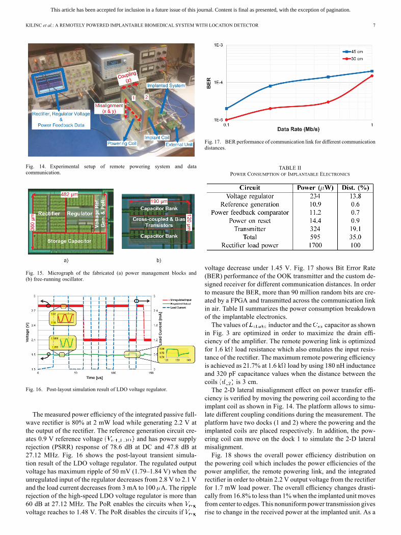
power amplifier is omitted to further reduce power dissipation.The inductor in the LC tank of the oscillator is implementedoff-chip to also serve as a transmitting antenna. The radiation ef-ficiency of an antenna is proportional to its effective area whichis limited by the implant size. Fig. 12 shows the loop antenna ofthe free-running oscillator transmitter. The antenna which hasa diameter of 11 mm is optimized in an electromagnetic sim-ulation program (Momentum) [40]. The simulated inductancevalue and the quality factor of the loop antenna are 28 nH and204, respectively. Two capacitive banks which are controlledby a digital block are also added to LC tank for tuning the os-cillation frequency to the operation frequency band (868 MHz).The total estimated radiation efficiency of this antenna is 3% infree space [41]. Therefore, the estimated radiated power fromthe implant in free space is dBm according to the simu-lated AC power dissipation of 30 W in the LC tank.Commercially available ISM band receivers tolerate only
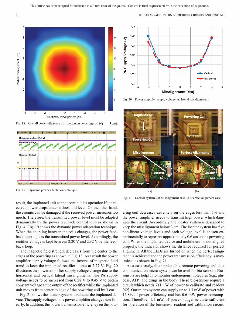
small frequency drifts. However, the low-power transmitter ofthe implanted system has a large frequency deviation whichneeds to be compensated by the receiver. Therefore, the re-ceiver is designed to demodulate signals with large carrierdrifts. Fig. 13 shows the block diagram of the proposed custom
Fig. 12. Loop antenna of free-running oscillator transmitter on a test board.
Fig. 13. Block diagram of proposed custom designed receiver.
designed receiver. The received signal is filtered by a ceramicbandpass filter which serves a high quality factor and sharptransition band. The filter has a 20 MHz bandwidth which iswide enough to detect the carrier signal with frequency driftsdue to temperature and LC tank variation of the implantedtransmitter.The data is transmitted as On-Off-Keying (OOK) modulated
signal. Therefore, a logarithmic amplifier (logamp) follows theRF amplifier in order to detect these RF bursts. The logampworks as an envelope detector and converts the input powerlevel to an output voltage. Finally, the output of the logampis compared to a reference voltage with the help of ahigh-speed comparator with a hysteresis for further immunityto noise. The data rate of the receiver can be as high as 1.5Mbps. The total power dissipation of the receiver is 152 mW.The minimum detectable signal at the input of the receiver is
dBm limited by the sensitivity of the logamp. The requiredsignal to noise ratio (SNR) and the sensitivity can be adjustedby changing the comparators reference voltage .In order to obtain reliable measurement results from sensors,
each sensor needs to be calibrated and biased properly due to thedifferent environmental conditions. Therefore, some low-datarate commands are transmitted from the external unit to the im-planted unit by modulating amplitude of the powering signal.The commands are received by a ASK demodulator in the im-planted unit and the demodulated information is processed bythe digital block.
VI. SIMULATION AND MEASUREMENT RESULTS
In order to validate the performance of the remotely poweredimplantable sensor system, an experimental setup is created.Fig. 14 shows the experimental setup of the remote poweringsystem for the implantable sensor unit. The circuits are fabri-cated in 0.18 m standard CMOS process. The rectifier and theregulator circuits are designed with 3.3 V thick transistors to in-crease the reliability and the longevity of the circuits. Fig. 15represents the micrograph of the fabricated circuits.
This article has been accepted for inclusion in a future issue of this journal. Content is final as presented, with the exception of pagination.
KILINC et al.: A REMOTELY POWERED IMPLANTABLE BIOMEDICAL SYSTEM WITH LOCATION DETECTOR 7
Fig. 14. Experimental setup of remote powering system and datacommunication.
Fig. 15. Micrograph of the fabricated (a) power management blocks and(b) free-running oscillator.
Fig. 16. Post-layout simulation result of LDO voltage regulator.
The measured power efficiency of the integrated passive full-wave rectifier is 80% at 2 mW load while generating 2.2 V atthe output of the rectifier. The reference generation circuit cre-ates 0.9 V reference voltage and has power supplyrejection (PSRR) response of 78.6 dB at DC and 47.8 dB at27.12 MHz. Fig. 16 shows the post-layout transient simula-tion result of the LDO voltage regulator. The regulated outputvoltage has maximum ripple of 50 mV (1.79–1.84 V) when theunregulated input of the regulator decreases from 2.8 V to 2.1 Vand the load current decreases from 3 mA to 100 A. The ripplerejection of the high-speed LDO voltage regulator is more than60 dB at 27.12 MHz. The PoR enables the circuits whenvoltage reaches to 1.48 V. The PoR disables the circuits if
Fig. 17. BER performance of communication link for different communicationdistances.
TABLE IIPOWER CONSUMPTION OF IMPLANTABLE ELECTRONICS
voltage decrease under 1.45 V. Fig. 17 shows Bit Error Rate(BER) performance of the OOK transmitter and the custom de-signed receiver for different communication distances. In orderto measure the BER, more than 90 million random bits are cre-ated by a FPGA and transmitted across the communication linkin air. Table II summarizes the power consumption breakdownof the implantable electronics.The values of inductor and the capacitor as shown
in Fig. 3 are optimized in order to maximize the drain effi-ciency of the amplifier. The remote powering link is optimizedfor 1.6 k load resistance which also emulates the input resis-tance of the rectifier. The maximum remote powering efficiencyis achieved as 21.7% at 1.6 k load by using 180 nH inductanceand 320 pF capacitance values when the distance between thecoils is 3 cm.The 2-D lateral misalignment effect on power transfer effi-
ciency is verified by moving the powering coil according to theimplant coil as shown in Fig. 14. The platform allows to simu-late different coupling conditions during the measurement. Theplatform have two docks (1 and 2) where the powering and theimplanted coils are placed respectively. In addition, the pow-ering coil can move on the dock 1 to simulate the 2-D lateralmisalignment.Fig. 18 shows the overall power efficiency distribution on
the powering coil which includes the power efficiencies of thepower amplifier, the remote powering link, and the integratedrectifier in order to obtain 2.2 V output voltage from the rectifierfor 1.7 mW load power. The overall efficiency changes drasti-cally from 16.8% to less than 1%when the implanted unit movesfrom center to edges. This nonuniform power transmission givesrise to change in the received power at the implanted unit. As a
This article has been accepted for inclusion in a future issue of this journal. Content is final as presented, with the exception of pagination.
8 IEEE TRANSACTIONS ON BIOMEDICAL CIRCUITS AND SYSTEMS
Fig. 18. Overall power efficiency distribution on powering coil ( cm).
Fig. 19. Dynamic power adaptation technique.
result, the implanted unit cannot continue its operation if the re-ceived power drops under a threshold level. On the other hand,the circuits can be damaged if the received power increases toomuch. Therefore, the transmitted power level must be adapteddynamically by the power feedback control loop as shown inFig. 4. Fig. 19 shows the dynamic power adaptation technique.When the coupling between the coils changes, the power feed-back loop adjusts the transmitted power level. Accordingly, therectifier voltage is kept between 2.20 V and 2.32 V by the feed-back loop.The magnetic field strength decreases from the center to the
edges of the powering as shown in Fig. 18. As a result the poweramplifier supply voltage follows the inverse of magnetic fieldtrend to keep the implanted rectifier output at 2.27 V. Fig. 20illustrates the power amplifier supply voltage change due to thehorizontal and vertical lateral misalignments. The PA supplyvoltage needs to be increased from 0.28 V to 0.45 V to obtainconstant voltage at the output of the rectifier while the implantedunit moves from center to edge of the powering coil by 3 cm.Fig. 21 shows the locator system to relocate the implanted de-
vice. The supply voltage of the power amplifier changes non-lin-early. In addition, the power transmission efficiency on the pow-
Fig. 20. Power amplifier supply voltage vs. lateral misalignment.
(a) (b)
Fig. 21. Locator system. (a) Misalignment case. (b) Perfect alignment case.
ering coil decreases extremely on the edges less than 1% andthe power amplifier needs to transmit high power which dam-ages the circuit. Accordingly, the locator system is designed tokeep the misalignment below 3 cm. The locator system has fivenon-linear voltage levels and each voltage level is chosen ex-perimentally to represent approximately 0.6 cm on the poweringcoil. When the implanted device and mobile unit is not alignedproperly, the indicator shows the distance required for perfectalignment. All the LEDs are turned on when the perfect align-ment is achieved and the power transmission efficiency is max-imized as shown in Fig. 21.As a case study, this implantable remote powering and data
communication micro-system can be used for bio-sensors. Bio-sensors are helpful to monitor endogenous molecules (e.g., glu-cose, ATP) and drugs in the body. These bio-sensors require acircuit which needs 711 W of power to calibrate and readout[42]. Our micro-system can supply up to 1.7 mW of power with16.8% of power efficiency and has 0.6 mW power consump-tion. Therefore, 1.1 mW of power budget is quite sufficientfor operation of the bio-sensor readout and calibration circuit.
This article has been accepted for inclusion in a future issue of this journal. Content is final as presented, with the exception of pagination.
KILINC et al.: A REMOTELY POWERED IMPLANTABLE BIOMEDICAL SYSTEM WITH LOCATION DETECTOR 9
TABLE IIISUMMARY OF REMOTELY POWERED IMPLANTABLE MICRO-SYSTEM
TABLE IVPERFORMANCE COMPARISON OF REMOTE POWERING LINK
TABLE VPERFORMANCE COMPARISON OF SHORT RANGE COMMUNICATION
Table III summarizes the performance of the remotely poweredimplantable micro-system. Furthermore, Tables IV and V com-pare this work with the recently reported remotely powered sys-tems and the short range communication systems in the litera-ture, respectively.
VII. CONCLUSION
The paper presents an universal remote powering and com-munication systems for the implantable medical devices to beused along with different sensor/actuator interfaces. A perma-nent implanted device is placed under the skin and stores themeasured data. A mobile external unit charges the implanteddevice and receives the data from the implant. A locator systemis proposed to relocate the implant in the body with 6 mm reso-lution for the efficient power transfer. A significant feature is thedetection of the location of the implant. Moreover, this custom
designed receiver tolerates large data carrier drifts of the trans-mitter. The fabricated implantable electronics works with a rel-atively low supply voltage and provides all the functions neededfor the external link thanks to an optimized remote power supplycapable to operate over 3 cm distance. The power required bythe implantable electronics including the one for the wirelesscommunication is just 0.6 mW.
ACKNOWLEDGMENT
The authors would like to thank to F. Mazzilli, G. Yilmaz,and O. Atasoy for their valuable feedback and help.
REFERENCES[1] E. Wilkins et al., “Integrated implantable device for long-term glucose
monitoring,” Biosens. Bioelectron., vol. 10, pp. 485–494, 1995.[2] S. Carrara et al., “Multi-panel drugs detection in human serum for
personalized therapy,” Biosens. Bioelectron., vol. 26, no. 9, pp.3914–3919, 2011.
[3] M. Sawan, Y. Hu, and J. Coulombe, “Wireless smart implants ded-icated to multichannel monitoring and microstimulation,” IEEE Cir-cuits Syst. Mag., vol. 5, no. 1, pp. 21–39, 2005.
[4] C. Boero et al., “New technologies for nanobiosensing and their ap-plications to real-time monitoring,” in Proc. IEEE Biomedical Circuitsand Systems Conf., 2011, pp. 357–360.
[5] N. Chaimanonart and D. J. Young, “A wireless batteryless in vivo EKGand body temperature sensing microsystem with adaptive RF poweringfor genetically engineered mice monitoring,” in Proc. Int. Solid-StateSensors, Actuators and Microsystems Conf., 2009, pp. 1473–1476.
[6] A. Prasad and M. Sahin, “Characterization of neural activity recordedfrom the descending tracts of the rat spinal cord,” Frontiers Neurosci.,vol. 4, no. 21, pp. 1–7, June 2010.
[7] E. G. Kilinc et al., “Remotely powered telemetry system with dynamicpower-adaptation for freely moving animals,” in Proc. IEEE Biomed-ical Circuits and Systems Conf., 2012, pp. 260–263.
[8] M. Azin et al., “A miniaturized system for spike-triggered intracorticalmicrostimulation in an ambulatory rat,” IEEE Trans. Biomed. Eng.,vol. 58, no. 9, pp. 2589–2597, 2011.
[9] C. T. Wentz et al., “A wirelessly powered and controlled device foroptical neural control of freely-behaving animals,” J. Neural Eng., vol.8, no. 4, 2011.
[10] E. G. Kilinc et al., “Short-range remote powering for long-term im-plantable sensor systems in freely moving small animals,” in Proc.IEEE Sensors Conf., 2013, pp. 1787–1790.
[11] E. G. Kilinc et al., “Short range remote powering of implanted elec-tronics for freely moving animals,” in Proc. IEEE 11th Int. New Cir-cuits and Systems Conf., 2013, pp. 1–4, 2013.
[12] D. C. Yates, A. S. Holmes, andA. J. Burdett, “Optimal transmission fre-quency for ultralow-power short-range radio links,” IEEE Trans. Cir-cuits Syst. I, Reg. Papers, vol. 51, no. 7, pp. 1405–1413, 2004.
[13] C. M. Zierhofer and E. S. Hochmair, “Geometric approach forcoupling enhancement of magnetically coupled coils,” IEEE Trans.Biomed. Eng., vol. 43, no. 7, pp. 708–714, 1996.
[14] U. M. Jow and M. Ghovanloo, “Modeling and optimization of printedspiral coils in air, saline, and muscle tissue environments,” IEEE Trans.Biomed. Circuits Syst., vol. 3, pp. 339–347, 2009.
[15] J. Ferreira, “Improved analytical modeling of conductive losses inmag-netic components,” IEEE Trans. Power Electron., vol. 9, no. 1, pp.127–131, 1994.
[16] S. Gabriel, R. W. Lau, and C. Gabriel, “The dielectric properties ofbiological tissues: II. Measurements on the frequency range 10 Hz to20 GHz,” Phys. Med. Biol., vol. 41, pp. 2251–2269, 1996.
[17] Ansys, Inc., USA., HFSS-3D Full-Wave Electromagnetic Field Simu-lation. [Online]. Available: http://www.ansoft.com/products/hf/hfss
[18] Inductive Applications ERC/REC 70-03, in Annex 9, Oct. 2009.[19] K. M. Silay, C. Dehollain, and M. Declercq, “Improvement of power
efficiency of inductive links for implantable devices,” in Proc.Ph.D. Research in Microelectronics and Electronics Conf., 2008, pp.229–232.
[20] E. G. Kilinc et al., “FoM to compare the effect of ASK based commu-nications on remotely powered systems,” in Proc. Ph.D. Research inMicroelectronics and Electronics Conf., 2011, pp. 29–32.
[21] K. V. Schuylenbergh and R. Puers, Inductive Powering. New York,NY, USA: Springer, 2009.

This article has been accepted for inclusion in a future issue of this journal. Content is final as presented, with the exception of pagination.
10 IEEE TRANSACTIONS ON BIOMEDICAL CIRCUITS AND SYSTEMS
[22] E. G. Kilinc, C. Dehollain, and F. Maloberti, “Design and optimiza-tion of inductive power transmission for implantable sensor system,”in Proc. Int. Workshop Symbolic and Numerical Methods, Modelingand Applications to Circuit Design, 2010, pp. 1–5.
[23] Fast Field Solvers [Online]. Available: http://www.fastfield-solvers.com
[24] N. O. Sokal, “Class-E RF power amplifiers,” QEX Mag., no. 204, pp.9–20, Jan./Feb. 2001.
[25] T. H. Lee, The Design of CMOS Radio-Frequency Integrated Cir-cuits. Cambridge, U.K.: Cambridge Univ. Press, 2004.
[26] M. Kiani and M. Ghovanloo, “An RFID-based closed loop wirelesspower transmission system for biomedical applications,” IEEE Trans.Circuits Syst. II, Exp. Briefs, vol. 57, no. 4, pp. 260–264, 2010.
[27] G. Wang et al., “Design and analysis of an adaptive transcutaneouspower telemetry for biomedical implants,” IEEE Trans. Circuits Syst.I, Reg. Papers, vol. 52, no. 10, pp. 2109–2117, 2005.
[28] H. Lee and M. Ghovanloo, “An integrated power-efficient active recti-fier with offset-controlled high speed comparators for inductively-pow-ered applications,” IEEE Trans. Circuits Syst. I, Reg. Papers, vol. 58,no. 8, pp. 1749–1760, 2011.
[29] O. Atasoy and C. Dehollain, “Remote powering realization for smartorthopedic implants,” in Proc. 10th IEEE Int. Conf. New Circuits andSystems, 2012, pp. 521–524.
[30] J.-P. Curty et al., “A model for -Power rectifier analysis and de-sign,” IEEE Trans. Circuits Syst. I, Reg. Papers, vol. 52, no. 12, pp.2771–2779, 2005.
[31] H. Nakamoto et al., “Passive UHF RF identification CMOS tag ICusing ferroelectric RAM in 0.35 m technology,” IEEE J. Solid-StateCircuits, vol. 42, no. 1, pp. 101–110, 2007.
[32] F. Mazzilli et al., “Design methodology and comparison of rectifiersfor UHF-band RFIDs,” in Proc. IEEE Radio Frequency Integrated Cir-cuits Symp., 2010, pp. 505–508.
[33] A. M. Sodagar et al., “Fully integrated CMOS power regulator fortelemetry-powered implantable biomedical microsystems,” in Proc.IEEE Custom Integrated Circuits Conf., 2006, pp. 659–662.
[34] M. Mi, RFID Radio Circuit Design in CMOS [Online]. Available:http://uqu.edu.sa/files2/tiny_mce/plugins/filemanager/files/4220086
[35] Non-spesific Short Range Devices ERC/REC 70-03, in Annex 1, Oct.2012.
[36] J. Pandey and B. P. Otis, “A sub-100 W MICS/ISM band transmitterbased on injection-locking and frequency multiplication,” IEEE J.Solid-State Circuits, vol. 46, no. 5, pp. 1049–1058, 2011.
[37] Y. H. Chee et al., “An ultra-low-power injection locked transmitter forwireless sensor networks,” IEEE J. Solid-State Circuits, vol. 41, no. 8,pp. 1740–1748, 2006.
[38] J. L. Bohorquez et al., “A 350 uW CMOS MSK transmitter and 400uW OOK super-regenerative receiver for medical implant communi-cations,” IEEE J. Solid-State Circuits, vol. 44, no. 4, pp. 1248–1259,2009.
[39] R. Harrison et al., “A low-power integrated circuit for a wireless 100-electrode neural recording system,” IEEE J. Solid-State Circuits, vol.42, no. 1, pp. 123–133, 2007.
[40] Agilent Technologies, Inc., USA,Momentum 3D Planar EM Simulator[Online]. Available: http://www.home.agilent.com/en/pc-1887116
[41] J. Pandey et al., “A fully integrated RF-powered contact lens with asingle element display,” IEEE Trans. Biomed. Circuits Syst., vol. 4, no.6, pp. 454–461, Dec. 2010.
[42] S. S. Ghoreishizadeh, S. Carrara, and G. De Micheli, “A configurableIC to contol, readout, and calibrate an array of biosensors,” in Proc.Eur. Conf. Circuit Theory and Design, 2013, pp. 1–4.
[43] M. Catrysse, B. Hermans, and R. Puers, “An inductive power systemwith integrated bidirectional data transmission,” inProc. 17th Eurosen-sors, Sep. 21–24, 2003, pp. 843–846.
[44] M. W. Baker and R. Sarpeshkar, “Feedback analysis and design of RFpower links for low-power bionic systems,” IEEE Trans. Biomed. Cir-cuits Syst., vol. 1, no. 1, pp. 28–38, Mar. 2007.
[45] U.-M. Jow and M. Ghovanloo, “Design and optimization of printedspiral coils for efficient transcutaneous inductive power transmission,”IEEE Trans. Biomed. Circuits Syst., vol. 1, no. 3, pp. 193–202, Sep.2007.
[46] A. K. RamRakhyani, S. Mirabbasi, and M. Chiao, “Design and opti-mization of resonance-based efficient wireless power delivery systemsfor biomedical implants,” IEEE Trans. Biomed. Circuits Syst., vol. 5,no. 1, pp. 48–63, Feb. 2011.
[47] K. M. Silay, C. Dehollain, and M. Declercq, “A closed-loop remotepowering link for wireless cortical implants,” IEEE Sensors J., vol. 13,no. 9, pp. 3226–3235, Sep. 2013.
[48] D. C. Daly and A. P. Chandrakasan, “An energy-efficient OOK trans-ceiver for wireless sensor networks,” IEEE J. Solid-State Circuits, vol.42, no. 5, pp. 1003–1011, May 2007.
[49] J. Jung, S. Zhu, P. Liu, Y.-J. Chen, and D. Heo, “22-pJ/bit energy-effi-cient 2.4-GHz implantable OOK transmitter for wireless biotelemetrysystems: In Vitro experiments using rat skin-mimic,” IEEE Trans. Mi-crow. Theory Tech., vol. 58, no. 12, pp. 4102–4111, Dec. 2010.
Enver G. Kilinc (S’11) was born in Istanbul, Turkey,in 1985. He received the B.Sc. degree in electronicengineering from Istanbul Technical University(ITU), Istanbul, Turkey, and the M.Sc. degree inelectrical and electronic engineering from EcolePolytechinque Fédérale de Lausanne (EPFL), Lau-sanne, Switzerland, in 2008 and 2010, respectively.In March 2010, he joined the Electronics Labo-
ratory at EPFL as a Research Assistant in the fieldof RFIC design. Currently, he is working toward thePh.D. degree on wireless power transmission and
radio frequency identification (RFID) with the RFIC Group, Swiss Federale In-stitute of Technology, Lausanne, Switzerland. His research interests include RFCMOS circuit design for wireless sensor systems and biomedical applications.
Mehrad A. Ghanad (S’13) received the B.S. degreein electrical engineering from the K. N. Toosi Uni-versity of Technology, Tehran, Iran, and the M.S. de-gree in microelectronic engineering from the SharifUniversity of Technology, Tehran, Iran, in 2007 and2009, respectively.Currently, he is working toward the Ph.D.
degree with the RFIC Group at Ecole Polytech-nique Fédérale de Lausanne (EPFL), Lausanne,Switzerland. His research interests include design oflow-power analog and RF CMOS integrated circuits.
Franco Maloberti (A’84–SM’97–F’96) receivedthe Laurea degree in physics (summa cum laude)from the University of Parma, Parma, Italy, and theDr. Honoris Causa degree in electronics from Inaoe,Puebla, Mexico, in 1968 and 1996, respectively.He was a Visiting Professor at ETH-PEL, Zurich,
Switzerland, in 1993 and at EPFL-LEG, Lausanne,Switzerland, in 2004. He was Professor of Micro-electronics and Head of theMicro Integrated SystemsGroup, University of Pavia, Pavia, Italy, TI/J. KilbyAnalog Engineering Chair Professor at Texas A&M
University, College Station, TX, USA, and the Distinguished MicroelectronicChair Professor at the University of Texas at Dallas. Currently, he is Professor atthe University of Pavia and Honorary Professor, University of Macau, Macau,China. His professional expertise is in the design, analysis, and characterizationof integrated circuits and analogue digital applications, mainly in the areas ofswitched capacitor circuits, data converters, interfaces for telecommunicationand sensor systems, and portable power management. He has written more than475 published papers, five books, and holds 32 patents. He has been respon-sible for many research programs, including 10 ESPRIT projects and served theEuropean Commission in many European Initiatives. He served the Academyof Finland on the assessment of electronic research, and the National ResearchCouncil of Portugal for the research activity assessment of Portuguese Univer-sities. He was a member of the Advisory Board of INESC-Lisbon, Portugal. Heis the Chairman of the Academic Committee of the Microelectronics Key Lab-oratory, Macau, China.Prof. Maloberti was VP Region 8 of IEEE CAS (1995–1997), Associate
Editor of the IEEE TRANSACTIONS ON CIRCUITS AND SYSTEMS-II: EXPRESSBRRIEFS, President of the IEEE Sensor Council (2002–2003), IEEE CAS BoGmember (2003–2005), and VP Publications IEEE CAS (2007–2008). He wasDL IEEE SSC Society (2009–2010) and currently is DL IEEE CAS Society.He received the 1999 IEEE CAS Society Meritorious Service Award, the 2000CAS Society Golden Jubilee Medal, and the IEEE Millenium Medal. He wascorecipient of the 1996 IEE Fleming Premium, the ESSCIRC 2007 Best PaperAward and the IEEJ Workshop 2007, and 2010 Best Paper Award.

This article has been accepted for inclusion in a future issue of this journal. Content is final as presented, with the exception of pagination.
KILINC et al.: A REMOTELY POWERED IMPLANTABLE BIOMEDICAL SYSTEM WITH LOCATION DETECTOR 11
Catherine Dehollain (M’93) received the Master’sdegree in electrical engineering and the Ph.D. degreefrom Ecole Polytechnique Fédérale de Lausanne(EPFL), Lausanne, Switzerland, in 1982 and 1995,respectivelyFrom 1982 to 1984, she was a Research Assistant
at the Electronics Laboratories (LEG), EPFL. In1984, she joined the Motorola European Center forResearch and Development, Geneva, Switzerland,where she designed integrated circuits applied totelecommunications. In 1990, she joined EPFL as a
Senior Assistant at the haire des Circuits et Systémes, where she was involved
in impedance broadband matching. Since 1995, she has been responsible forthe RFIC Group, EPFL, for RF activities. She has been the Technical ProjectManager of the European projects, CTI projects, and the Swiss NationalScience Foundation projects dedicated to RF wireless micropower sensornetworks and mobile phones. Since 1998, she has been a Lecturer at EPFL inthe area of RF circuits, electric filters, and CAD tools. Since 2006, she has beena Maítre d’Enseignement et de Recherche, EPFL. She is an author or coauthorof four scientific books and 110 scientific publications. Her current researchinterests include low power analog circuits, biomedical remotely poweredsensors, and electric filters.
![IEEE TRANSACTIONS ON BIOMEDICAL CIRCUITS AND …by wires to biomedical sensors, e.g., the Holter monitors [1]. Recent advancements in microelectronics and radio communi-cation have](https://img.pdfslide.net/doc/110x75/5f34d1ae94276c2f9b18625f/ieee-transactions-on-biomedical-circuits-and-by-wires-to-biomedical-sensors-eg.jpg)