Embed Size (px)
Citation preview
(19) United States US 2009025 1235A1
(12) Patent Application Publication (10) Pub. No.: US 2009/0251235 A1 Belot et al. (43) Pub. Date: Oct. 8, 2009
(54) BULK ACOUSTICWAVE RESONATOR FILTER BEING DIGITALLY RECONFIGURABLE, WITH PROCESS
(75) Inventors: Didier Belot, Rives (FR): Alexandre Augusto Shirakawa, Talence (FR); Eric Kerherve, Talence (FR); Moustapha El Hassan, Talence (FR); Yann Deval, Bordeaux (FR)
Correspondence Address: SEED INTELLECTUAL PROPERTY LAW GROUP PLLC 701 FIFTHAVENUE, SUITE 5400 SEATTLE, WA 98104-7092 (US)
(73) Assignees: STMICROELECTRONICS S.A., Montrouge (FR); Centre National de la Recherche Scientifique (C.N.R.S.), Paris (FR)
(21) Appl. No.: 12/371,415
39 . . . . . . . . . . . . .N? ...e.:::::::::::::::: 33 II - D - i? ... 32iss 336ss.
(22) Filed: Feb. 13, 2009
(30) Foreign Application Priority Data
Feb. 15, 2008 (FR) ...................................... O8 OO827
Publication Classification
(51) Int. Cl. HO3H 9/02 (2006.01)
(52) U.S. Cl. ........................................................ 333/187
(57) ABSTRACT
A filtering circuit with BAW type acoustic resonators having at least a first quadripole and a second quadripole connected in cascade, each quadripole having a branch series with a first acoustic resonator of type BAW and a branch parallel with each branch having an acoustic resonator of type BAW, the first acoustic resonator having a frequency of resonance series approximately equal to the frequency of parallel resonance of the second acoustic resonator, the branch parallel of the first quadripole having a first capacitance connected in series with the second resonator and, in parallel with the capacitance, a first Switching transistor to short circuit the capacitance.
Ts.
325 3. N 331 N y. -- :- ...'.... . . . . . . .... re... --re.
323

Patent Application Publication Oct. 8, 2009 Sheet 1 of 8 US 2009/0251235 A1
FIG, 1A

Patent Application Publication Oct. 8, 2009 Sheet 2 of 8 US 2009/0251235 A1
44 -
----------
1E3 = | | | IAN ...................i................................................ MINIMI
1 E.
E-me

US 2009/0251235 A1 Oct. 8, 2009 Sheet 3 of 8 Patent Application Publication
Patent Application Publication Oct. 8, 2009 Sheet 4 of 8 US 2009/0251235 A1
E.
Ea
tE3
A. f Vitt E.
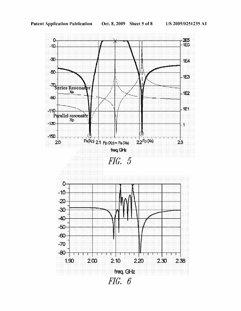
Patent Application Publication Oct. 8, 2009 Sheet 5 of 8 US 2009/0251235 A1
-) Parallel resonator f
t
150 M M M -----------I. Accorror 2. sp21 Fp(xorsts 22Fp(XS) 23
eight.
FIG. 5

US 2009/0251235 A1 Oct. 8, 2009 Sheet 6 of 8 Patent Application Publication

Patent Application Publication Oct. 8, 2009 Sheet 7 of 8 US 2009/0251235 A1
190 200 2.10 220 230 2.38 freq, GHz
FIG BA
HVTNH www.www.wawasawa?????-?????
1.90 200 210 220 230 238 freq. Ghiz
FIG. BB

Patent Application Publication Oct. 8, 2009 Sheet 8 of 8 US 2009/0251235 A1
190 200 210 220 230 238
-0 || ART | 2. AAA

US 2009/025 1235 A1
BULKACOUSTC WAVE RESONATOR FILTER BEING DIGITALLY
RECONFIGURABLE, WITH PROCESS
BACKGROUND
0001 1. Technical Field 0002 The present disclosure relates to electronic circuits and more particularly to a filtering circuit with Bulk Acoustic Wave (BAW) resonators that can be digitally reconfigured. 0003 2. Description of the Related Art 0004 Today acoustic resonators are widespread in con Sumer applications but also in professional applications because of their high efficiency, including the realization of high performance band pass filters, and in particular in mobile telephony for the selection of transmission channels. 0005 Research has been conducted on two types of acous
tic resonators that show remarkable performance, namely the SAW resonators (Surface Acoustic Wave Resonator) and, more recently, the BAW (Bulk Acoustic Wave Resonator). In the first type, the acoustic resonator is located on the Surface of a semiconductor product while in BAWs it lays inside a volume delimited between a lower electrode and a higher electrode so that the acoustic wave develops in this volume. BAW resonators are the subject of wide research from manu facturers of semi-conductor products because those compo nents allow consideration of a high degree of integration of filtering circuits, thus allowing significant manufacturing costs savings. 0006 BAW resonators allow higher frequencies than those used with SAWs, while achieving more compact struc tures.
0007 Beyond the performance offered by BAW resona tors for the realization of a digital filter, there is a need for easy configuration of filtering characteristics of a filter made of BAW resonators. 0008 Such configuring has been achieved, so far, by using varactors connected in series or in parallel with the resonators and which are controlled by the application of an analog Voltage. 0009. Such a device, if it has some merit, however, requires a complex control and thus a Sophisticated analog circuitry. 0010. It is desirable to simplify the design of the command of the adjustment of acoustic resonators used in filtering circuits to allow, in particular, a more Sophisticated command while being less costly to implement.
BRIEF SUMMARY
0011. The present disclosure is directed to a structure of filters—suitable for mobile telephony—made of BAW acous tic resonators that are easily configurable. The present disclo sure also provides a low cost filter fitted with acoustic reso nators that allows a complete digital control of the frequency response. The present disclosure further provides a filtering circuit with BAW resonators integrated on a substrate of semiconductor material and which can be easily digitally configured. 0012. In accordance with one embodiment, a BAW acous
tic resonators filtering circuit is provided that includes at least a first and a second quadripole connected in cascade, each quadripole comprising a series branch with a first BAW type acoustic resonator and a parallel branch with a second BAW type acoustic resonator. The first BAW resonator has a fre
Oct. 8, 2009
quency of the series resonance that is approximately equal to the frequency of the parallel resonance of the second acoustic reSOnatOr.
0013 The circuit is characterized in that the parallel branch of the first quadripole includes a first capacitance that is connected in series with the second resonator, and which is connected in parallel with that capacitance, a first Switching transistor controlled by a first control Voltage for performing a short circuit of that capacitance. 0014. In one embodiment, the second quadripole includes a second capacitance connected in series with the second resonator and, in parallel with the latter, a second Switching transistor controlled by a second control Voltage and designed for performing a short circuit of that capacitance. 0015 Thus the control voltages of the first, the second (and more when appropriate) Switching transistors may be conveyed through a control bus that allows a fully digital control of the filtering characteristics of the acoustic resona tor filtering circuit. 0016 One can thus, from the outset, perform a full digital control of the filtering circuit by appropriate digital process ing. The use of analog components, such as the expensive and not so easy to use Varactors, can thus be avoided. 0017. In one particular embodiment, the resonators are all of the Surface Mounted Resonator (SMR) type and are arranged on a mirror of Bragg. 0018. In one particular embodiment, the filtering circuit is used to achieve a reception circuit in mobile telephony of the 4th generation. 0019. The disclosure also achieves a process of reducing the interference suffered by a receiver in a mobile telephone comprising a filtering circuit based on a cascade of cells, each having a parallel branch with a first acoustic resonator type BAW, and a serial branch with a second acoustic resonator type BAW, that second BAW mounted in series with a capaci tance having a Switching transistor connected to its terminals. 0020. The process includes the following steps:
0021 detecting the presence of a signal disturbance in the close vicinity of one band being used for communi cations with one mobile telephone and which might disturb that communication; and
0022 digital control, in response to a possible detec tion, of one or more transistors in order to introduce the effect of capacitances connected in series with the reso nators of parallel branches so as to change the poles of the filter and increase its selectivity
0023. In accordance with another embodiment of the present disclosure, a circuit is provided that includes a plu rality of series-coupled quadripole cells, each cell having first and second inputs and first and second outputs, the first and second outputs coupled to first and second inputs of an adja cent quadripole cell, with the first and second outputs of a last cell in the plurality of cells forming an output of the circuit. Each cell further includes a series branch having a first acous tic resonator coupled between the first input and the first output, a parallel branch coupled between the first input and the first output and having coupled in series a second acoustic resonator and a capacitance with a Switching transistor coupled in parallel with the capacitance. The first acoustic resonator has a series resonant frequency that is approxi mately equal to a parallel resonant frequency of the second acoustic resonator. 0024. In accordance with another aspect of the foregoing embodiment, the acoustic resonators are of the BAW type.
US 2009/025 1235 A1
Preferably, the BAW resonators are Surface Mounted Reso nators arranged on a mirror of Bragg. 0025. In accordance with another aspect of the foregoing embodiment, the first acoustic resonator has a series resonant frequency that is approximately equal to the parallel resonant frequency of the second acoustic resonator in each of the quadripole cells. 0026. In accordance with another aspect of the foregoing embodiment, each of the Switching transistors are coupled to a digital control bus used for tuning the circuit. 0027. In accordance with another embodiment of the present disclosure, a circuit is provided that includes a plu rality of resonator cells coupled in series, and including at least: a first resonator cell that has two inputs and two outputs, an acoustic resonator coupled in series between the first input and the second output, and a series coupled resonator and capacitance coupled between the first input and the second output, and a Switching transistor coupled in series with the capacitance to short-circuit the capacitance; a second resona tor cell in the plurality of series-coupled resonator cells hav ing first and second inputs coupled to the respective first and second outputs of the first quadripole cell, first and second outputs, a resonator coupled in series between the first input and the first output, and a second resonator coupled between the first input and the second input; and at least a third reso nator cell in the plurality of series-coupled resonator cells having first and second inputs coupled to the first and second outputs of the second resonator cell and a series coupled resonator and capacitance coupled between the first and sec ond inputs, and a Switching transistor coupled in parallel with the capacitance to short-circuit the capacitance. 0028. In accordance with another aspect of the foregoing embodiment, the circuit has a series resonant frequency that is
1 Co - C - C f = 2 (CC, La + CoCaLa)
BRIEF DESCRIPTION OF THE SEVERAL VIEWS OF THE DRAWINGS
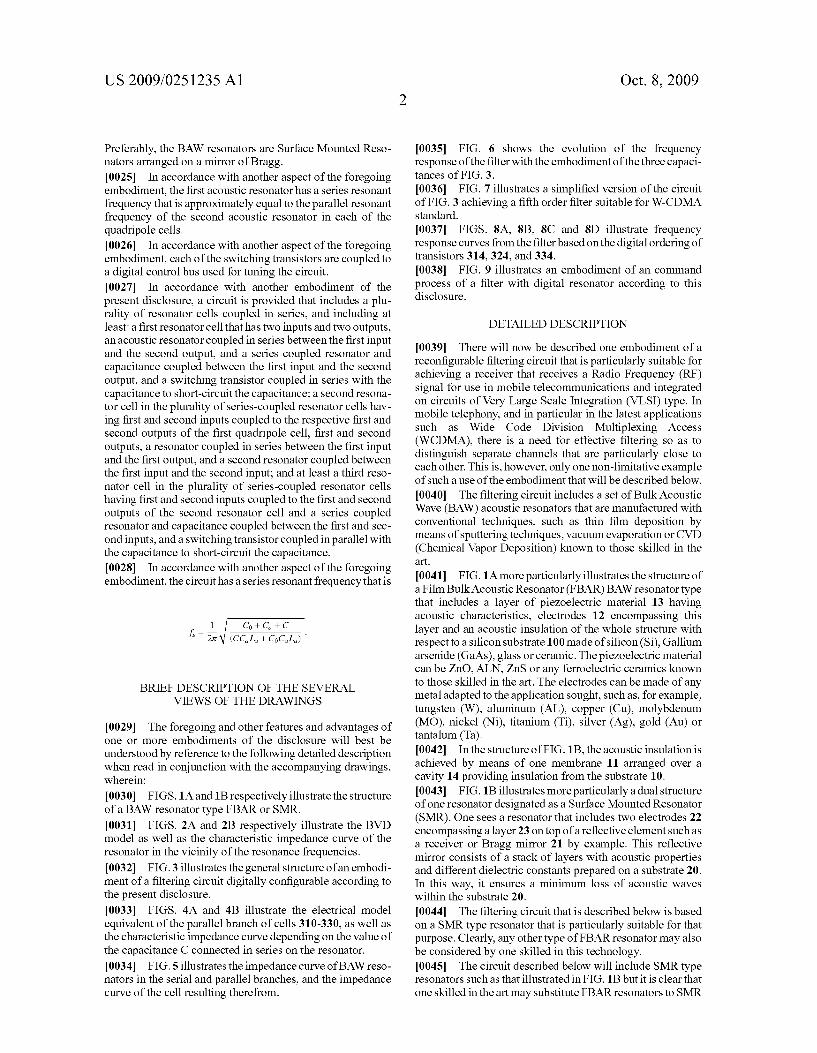
0029. The foregoing and other features and advantages of one or more embodiments of the disclosure will best be understood by reference to the following detailed description when read in conjunction with the accompanying drawings, wherein:
0030 FIGS. 1A and 1B respectively illustrate the structure of a BAW resonator type FBAR or SMR. 0031 FIGS. 2A and 2B respectively illustrate the BVD model as well as the characteristic impedance curve of the resonator in the vicinity of the resonance frequencies. 0032 FIG.3 illustrates the general structure of an embodi ment of a filtering circuit digitally configurable according to the present disclosure. 0033 FIGS. 4A and 4B illustrate the electrical model equivalent of the parallel branch of cells 310-330, as well as the characteristic impedance curve depending on the value of the capacitance C connected in series on the resonator. 0034 FIG.5 illustrates the impedance curve of BAW reso nators in the serial and parallel branches, and the impedance curve of the cell resulting therefrom.
Oct. 8, 2009
0035 FIG. 6 shows the evolution of the frequency response of the filter with the embodiment of the three capaci tances of FIG. 3. 0036 FIG. 7 illustrates a simplified version of the circuit of FIG.3 achieving a fifth order filter suitable for W-CDMA standard. 0037 FIGS. 8A, 8B, 8C and 8D illustrate frequency response curves from the filter based on the digital ordering of transistors 314, 324, and 334. 0038 FIG. 9 illustrates an embodiment of an command process of a filter with digital resonator according to this disclosure.
DETAILED DESCRIPTION
0039. There will now be described one embodiment of a reconfigurable filtering circuit that is particularly suitable for achieving a receiver that receives a Radio Frequency (RF) signal for use in mobile telecommunications and integrated on circuits of Very Large Scale Integration (VLSI) type. In mobile telephony, and in particular in the latest applications such as Wide Code Division Multiplexing Access (WCDMA), there is a need for effective filtering so as to distinguish separate channels that are particularly close to each other. This is, however, only one non-limitative example of such a use of the embodiment that will be described below.
0040. The filtering circuit includes a set of Bulk Acoustic Wave (BAW) acoustic resonators that are manufactured with conventional techniques, such as thin film deposition by means of sputtering techniques, vacuum evaporation or CVD (Chemical Vapor Deposition) known to those skilled in the art
0041 FIG. 1A more particularly illustrates the structure of a Film Bulk Acoustic Resonator (FBAR) BAW resonator type that includes a layer of piezoelectric material 13 having acoustic characteristics, electrodes 12 encompassing this layer and an acoustic insulation of the whole structure with respect to a silicon substrate 100 made of silicon (Si), Gallium arsenide (GaAs), glass or ceramic. The piezoelectric material can be ZnO, ALN, ZnS or any ferroelectric ceramics known to those skilled in the art. The electrodes can be made of any metal adapted to the application sought, Such as, for example, tungsten (W), aluminum (AL), copper (Cu), molybdenum (MO), nickel (Ni), titanium (Ti), silver (Ag), gold (Au) or tantalum (Ta). 0042. In the structure of FIG. 1B, the acoustic insulation is achieved by means of one membrane 11 arranged over a cavity 14 providing insulation from the substrate 10. 0043 FIG.1B illustrates more particularly a dual structure of one resonator designated as a Surface Mounted Resonator (SMR). One sees a resonator that includes two electrodes 22 encompassing a layer 23 on top of a reflective element such as a receiver or Bragg mirror 21 by example. This reflective mirror consists of a stack of layers with acoustic properties and different dielectric constants prepared on a substrate 20. In this way, it ensures a minimum loss of acoustic waves within the substrate 20.
0044) The filtering circuit that is described below is based on a SMR type resonator that is particularly suitable for that purpose. Clearly, any other type of FBAR resonator may also be considered by one skilled in this technology. 0045. The circuit described below will include SMR type resonators such as that illustrated in FIG.1B but it is clear that one skilled in the art may substitute FBAR resonators to SMR
US 2009/025 1235 A1
resonators and the disclosure is, in no way, limited by the particular acoustic insulation used for forming the BAW reso natOr.
0046 Generally speaking, the manufacturing process of a BAW-type, a FBAR type or a SMR type resonator is well known and will not be further described. The resonance fre quencies typically vary from 0.5 GHZ to 5 GHZ and those values closely depend upon the nature of material composing the resonator and also from the thickness of the layers being used. 0047. In particular, the two resonance frequencies are characteristics of the nature of the piezoelectric material being used (ZnO, ALN, ZnS or any known ferroelectric ceramics. 0048 FIG. 2A illustrates the electrical diagram equivalent of a resonator BAW, typically referred to as Butterworth Van Dyke (BVD), with parameters Ra, La and Cabeing represen tative of the frequency of the acoustic resonance frequency and also the acoustic losses. More particularly, La represents the equivalent series inductance and Ca represents the equiva lent series capacitance of the BAW resonator. The value of the capacitance C0 shown in FIG. 2A corresponds to the physical capacitance between the two electrodes of the resonator. 0049 FIG.2B illustrates the characteristic curve of a reso nator, showing two resonances, respectively series (cos corre sponding to a minimum impedance) and parallel (cop corre sponding to a maximum impedance). Outside the vicinity of the two resonances, the resonator tends to behave like a capacitance. 0050. The values (os and cop of the series and parallel resonances depend on the thickness of the piezoelectric mate rial, and the gap between these two values results from the electromechanical coupling coefficient. 0051. The BVD equivalent diagram shows an impedance that can be calculated using a simplified formula:
0052. There is now described with respect to FIG. 3 one embodiment of a filter.
0053. The filter consists of a set of cells, 310, 320, 330 respectively, each forming one quadripole. 0054 Cell 310 has two inputs, 301 and 302 respectively, and two outputs (bearing no reference numbers) that are connected at the two inputs of the quadripole forming the next cell320, etc. In FIG.3, one sees that the quadripole of the cell 330 has two exits 303 and 304, which are the output elec trodes of the filter.
0055. Each quadripole composing the cells 310,320,330 comprises a series branch (respectively 315,325,335) with a first resonator BAW (respectively 311, 321, 331) and a par allel branch (resp. 316, 326,336) with a second resonator BAW (resp. 312, 322, 332). BAW resonators (respectively 312,322,332) of the parallel branch are sized so as to show a parallel resonance frequency (anti-resonance) that is approxi mately equal to the serial resonance frequency of the particu lar resonator BAW (respectively 311, 321, 3312) located in the series branch of the same cell.
0056. In the embodiment shown in FIG. 3, each of the parallel branches 316 and 326 have a capacitance (respec
Oct. 8, 2009
tively 313, 323,333) connected in series with the parallel resonator BAW (respectively 312,322,332). 0057. In addition, a MOS transistor (respectively 314,324 and 334) has two electrodes source and drain that are con nected in parallel with the capacitance (respectively 313,323, 333) and further includes a gate electrode receiving a control Voltage for short-circuiting, when appropriate, the corre sponding capacitance. 0058 FIG. 3 shows a set of three identical cells that are cascaded, each including one capacitance (resp. 313,323 and 333) that enables significant control of the characteristics of the individual cell.
0059. It should be observed, however, that it is not essen tial that all the cells within the cascade of cells include one capacitance, and that one skilled in the art may consider that one or more particular cells will not include one capacitance within the parallel branch. 0060. Therefore, FIG. 3 illustrates one embodiment of a filtering circuit including BAW resonators included in both the series and the parallel branches of each cell, providing a set of terminals receiving the control voltages that form a full digital bus allowing full digital control of the acoustic char acteristics of the resonators.
0061 The circuit in FIG. 3 thus provides a particularly simple but effective solution for carrying out a digital control interface for a filter fitted with BAW resonators allowing Sophisticated digital processing. 0062 By applying on the set of gate electrodes an appro priate control voltage—either “0” or “1” one can set the characteristics of operation of the different acoustic resona tors and thus, eventually achieve, a fully digital control, directly from a Digital Signal Processor (DSP) of the whole response of the entire acoustic filter without requiring the use of any digital-to-analog converter. 0063 For the sake of clarity, it is represented in FIGS. 4A and 4B the electrical model equivalent of the parallel branch of cells 310-330, and the characteristic impedance curve depending on the value of the capacitance C connected in series on the resonator. 0064 Generally speaking, the capacitances are passive components that have a quality factor whose value lies in a range of 30 to 50. Furthermore, in the described embodiment, the capacitances are integrated into the parallel branch, bring ing little harm to the overall quality factor of the cell filter. This is a significant advantage of the circuit filter described, despite its apparent simplicity. 0065. Looking at, from a theoretical point of view, the effect of the introduction of the capacitance 313 in the parallel branch which includes resonator 312, the impedance can be calculated by the formula below:
Z s' (CC. L. + CoCL) + Co. + C + C (I) - SC(s2CoCaL + Co. + C)
0.066 Attention is drawn to the introduction of one pole and one Zero compared to the value of the impedance of a single parallel resonator. The calculations of extrapolation of the pole and the Zero lead to the following formulas (II) and (III):
US 2009/025 1235 A1
s’(CC. L. + CoCaLa)+ Co. + C + C = 0 (II) 2- Co - C - C
(CC, La + Co. Ca Lc.)
SC(s°CoCaL + Co. + C) = 0 (III) Co - C = 0 and s = - S alCS CoCaLa
Equation (III) shows the insertion of a pole at the frequency Zero, but one observes that other values are not changed. The equation (II) also shows that the connection of a capacitance in series with a resonator leads to the alteration of zeros in the frequency response. More specifically, by introducing a value of capacitance, one notes that the frequency of resonance series is shifted to the left, while the static value of the capaci tance of the resonator tends to decrease.
0067 FIG. 4B illustrates more particularly this effect because of the introduction of a capacitance in series with a resonator located in the parallel branch of a cell. As seen in FIG. 4B, the so-called SERIES resonators (designated by Xs indicating that the resonator is in series) have resonance fre quencies slightly higher than the so-called PARALLEL reso nators (or Xp). The series resonance (cps) of resonators PAR ALLEL, determine the position of the Zeros so that a variation of the impedance results in a corresponding change in those ZOS.
0068 Referring again to the BVD model, the values of frequencies of resonance series and parallel are given by the following formulas:
1 1
Js 2. WLC, 1 C + Co.
f 2. La CaCo
0069. Following the introduction of a value of capacitance C, and referring to the previous formula (II), the frequency of the resonance series becomes then:
1 Co - C - C f = 2 (CCL + Co.C. L.)
0070 A fine tuning of the filter characteristics can be achieved by changing one or more cells making up the filterin FIG. 3.
0071 FIG. 6 illustrates the change in the frequency response of the filter which results from the use of all three capacitances 313,323 and 333. 0072 FIG. 7 shows a simplified version 700 of the circuit
filter of FIG. 3 with only three cells 710, 720 and 730. Cell 710 is identical to cell 310 shown in FIG. 3. Cell 720 has no capacitance in its parallel branch, whereas cell 730 comprises no BAW resonator in its branch series, unlike cell 330 of FIG. 3
0073 For the sake of clarity, the elements that are identical in FIGS. 3 and 7 still carry the same reference numbers, and
Oct. 8, 2009
one sees that filter 700 differs from the filter illustrated in FIG. 3 in that capacitance 323, transistor 324 and resonator 331 have been removed. 0074 FIG. 7 therefore illustrates a filter of the 5th order, which shows to be less costly to manufacture and which provides fine and fully digital control by means of control voltages applied on the gates of transistors 314 and 334. Such a low cost circuit is suitable for use with a receiver complying with the standard WCDMA (2110-2170 MHz). (0075 Indeed FIG.8A shows the frequency response of the filter when transistors 314 and 334 are both switched on, respectively short-circuiting capacitances 313 and 333. In this configuration, filter (2103-2177 MHz) does not fit the W-CDMA standard. 0076. In order to improve the situation and comply with the standard, a blocking of transistor 314 can be used— causing the use of capacitance 313—and thus entailing a reduction of 20% of the bandwidth of the filter (2110-2170 MHz), as illustrated in FIG. 8B. The effect resulting from the insertion of the capacitance 313 on the displacement of Zeros is illustrated in FIG. 8C. 0077 Finally, the blocking of the two transistors 314 and 334 further reduces the bandwidth by the combined effect of both capacitances. 0078. This reduction is reflected in the frequency response curve of FIG. 8D. 007.9 The disclosure can be advantageously used in mobile wireless communication, when a receiver is located in one particular area where another mobile telephone is found to generate a signal which might interfere and disrupt the operation of the receiver and one ongoing communication. 0080. In such a situation, it is particularly advantageous to control the transistors in parallel branches to shift the poles and increase the selectivity of the circuit, for example by increasing the latter by 30 dB. 0081. The various embodiments described above can be combined to provide further embodiments. All of the U.S. patents, U.S. patent application publications, U.S. patent applications, foreign patents, foreign patent applications and non-patent publications referred to in this specification and/or listed in the Application Data Sheet are incorporated herein by reference, in their entirety. Aspects of the embodiments can be modified, if necessary to employ concepts of the various patents, applications and publications to provide yet further embodiments. I0082. These and other changes can be made to the embodi ments in light of the above-detailed description. In general, in the following claims, the terms used should not be construed to limit the claims to the specific embodiments disclosed in the specification and the claims, but should be construed to include all possible embodiments along with the full scope of equivalents to which Such claims are entitled. Accordingly, the claims are not limited by the disclosure.
1. A filtering circuit, comprising: BAW type acoustic resonators that each have at least a first,
a second, and a third cascade connected quadripole, each quadripole having a series branch comprising a first BAW type acoustic resonator and a parallel branch com prising a second BAW type acoustic resonator, said first acoustic resonator having a frequency of resonance series that is approximately equal to the frequency of the parallel resonance of the said second acoustic resonator;
wherein said parallel branch of said first quadripole includes a first capacitance connected in series with
US 2009/025 1235 A1
second resonator and, in parallel with that capacitance, a first Switching transistor for short-circuiting said capaci tance, said Switching transistor receiving a control Volt age from a digital bus under control of a digital signal processor.
2. The filtering circuit of claim 1 wherein the said second quadripole includes a second capacitance connected in series with the said second resonator and, in parallel with that said capacitance, a second Switching transistor for short-circuiting said capacitance.
3. The filtering circuit of claim 2 wherein the control volt ages of said first and second Switching transistors are part of a digital control bus used for tuning the filtering circuit.
4. The filtering circuit of claim 1 wherein the resonators are Surface Mounted Resonator type resonators arranged on a mirror of Bragg.
5. The filtering circuit of claim 1 wherein it is used with a receiver for a mobile telephone.
6. The filtering circuit with acoustic resonators according to claim 1 adapted to the W-CDMA norm having: A first quadripole with two input electrodes, two output
electrodes, and two branches, respectively series and parallel, wherein said series branch comprises a first BAW type
resonator having two frequencies of resonance, respectively series and parallel,
wherein said parallel branch comprises a second BAW type resonator having two frequencies of resonance, respectively series and parallel,
wherein the frequency of parallel resonance of said sec ond resonator are set to correspond to the frequency of resonance series of said first resonator,
wherein said parallel branch comprises a first capaci tance connected in series with said second resonator and, in parallel on said, a Switching transistor for performing a short-circuit of said capacitance under control of a first control Voltage;
a second quadripole connected in cascade with said first quadripole, and having two input electrodes, two output electrodes, and two branches, respectively series and parallel, wherein said series branch series comprises a third BAW
type resonator having two frequencies of resonance, respectively series and parallel,
wherein said parallel branch comprises a fourth BAW type resonator having two frequencies of resonance, respectively series and parallel,
wherein said frequency of resonance parallel of said fourth resonator is set to correspond to the frequency of resonance series of the said third resonator;
a third quadripole connected in cascade behind said second quadripole, and having two input electrodes, two output electrodes, and two branches, respectively series and parallel, wherein said series branch is without any resonator, wherein said parallel branch of said third quadripole has
a BAW type resonator having two frequencies of reso nance, respectively series and parallel,
wherein said frequency of resonance parallel of said fifth resonator is set to correspond to the frequency of resonance series of said third resonator,
wherein said parallel branch comprises a second capaci tance in series with said fifth resonator and, in parallel with said second capacitance, a second Switching
Oct. 8, 2009
transistor for performing a short-circuit of said capacitance under control of a second control Voltage.
7. The filtering circuit according to claim 6, comprising SMR type BAW resonators.
8. A process for reducing the interference of a receiver for a mobile telephone with a filtering circuit based on a cascade of cells, each having a parallel branch comprising a first BAW and a series branch comprising a second BAW, said second BAW connected in series with a capacitance having a Switch ing transistor connected in parallel, the process comprising:
detecting the presence of a disturbance signal near the mobile band used by the receiver for an ongoing com munication;
in response to said detection, controlling one or more of said Switching transistors directly through a digital con trol bus in order to modify the effect of the capacitance in the frequency response of the filter.
9. The process of claim 8 wherein the resonators comprise resonators of the SMR type.
10. The process of claim 8, comprising using the process in a 4th generation mobile telephone.
11. A circuit, comprising: a plurality of series-coupled quadripole cells, each cell
comprising: first and second inputs and first and second outputs, the
first and second outputs coupled to first and second inputs of an adjacent quadripole cell, with the first and second outputs of a last cell in the plurality of cells forming an output of the circuit;
a series branch comprising a first acoustic resonator coupled between the first input and the first output;
a parallel branch coupled between the first input and the first output and having coupled in series a second acoustic resonator and a capacitance, with a Switching transistor coupled in parallel with the capacitance;
the first acoustic resonator having a series resonant fre quency that is approximately equal to a parallel reso nant frequency of the second acoustic resonator.
12. The circuit of claim 11 wherein the first and second acoustic resonators comprise BAW type acoustic resonators.
13. The circuit of claim 11 wherein the switching transistor short-circuits the capacitance when the Switching transistoris turned on.
14. The circuit of claim 11 wherein each switching tran sistor of each quadripole cell is coupled to a control bus for tuning the circuit.
15. The circuit of claim 11 wherein the acoustic resonators comprise Surface Mounted Resonators arranged on a mirror of Bragg.
16. A circuit, comprising: a plurality of resonator cells coupled in series, and com
prising at least a first resonator cell having two inputs and two outputs, an acoustic resonator coupled in series between the first input and the second output, and a series coupled resonator and capacitance coupled between the first input and the second output, and a Switching transistor coupled in series with the capaci tance to short-circuit the capacitance;
a second resonator cell in the plurality of series-coupled resonator cells having first and second inputs coupled to the respective first and second outputs of the first reso nator cell and first and second outputs, a resonator coupled in series between the first input and the first

US 2009/025 1235 A1
output, and a second resonator coupled between the first input and the second input; and
at least a third resonator cell in the plurality of series coupled resonator cells having first and second inputs coupled to the first and second outputs of the second resonator cell and a series coupled resonator and capaci tance coupled between the first and second inputs, and a Switching transistor coupled in parallel with the capaci tance to short-circuit the capacitance.
17. The circuit of claim 16 wherein each of the acoustic resonators in each of the resonator cells comprises a resonator of the BAW type.
18. The circuit of claim 17 wherein each of the BAW resonators comprises a Surface mounted resonator arranged on a mirror of Bragg.
19. The circuit of claim 16 wherein the switching capaci tors are coupled to a digital control bus fortuning the circuit.
Oct. 8, 2009
20. The circuit of claim 16 wherein the series coupled resonator cells comprise a bulk acoustic wave resonator filter of the fifth order.
21. The circuit of claim 16 wherein a series resonant fre quency of each resonator cell comprises:
1 Co - C - C ?. 2 WCCL, C.C.L.)
wherein C represents the value of the capacitance, C, rep resents the equivalent circuit series capacitance at the acoustic resonant frequency, Co corresponds to the physical capacitance between electrodes of the resona tor, and L, represents the equivalent circuit series induc tance at the acoustic resonant frequency.
c c c c c
![arXiv:1702.03057v3 [stat.CO] 16 Oct 2017 · yINRIA Bordeaux, 200 Avenue de la Vieille Tour, 33405 Talence, FR. zDepartment of Statistics and Applied Probability, National University](https://img.pdfslide.net/doc/110x75/5f683dc72712d56665178ea2/arxiv170203057v3-statco-16-oct-2017-yinria-bordeaux-200-avenue-de-la-vieille.jpg)