Embed Size (px)
Citation preview
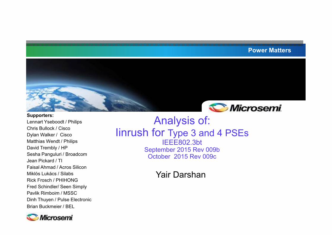
Power Matters
Analysis of:Iinrush for Type 3 and 4 PSEs
IEEE802.3btSeptember 2015 Rev 009b
October 2015 Rev 009c
Yair Darshan
Supporters:
Lennart Yseboodt / Philips
Chris Bullock / Cisco
Dylan Walker / Cisco
Matthias Wendt / Philips
David Trembly / HP
Sesha Panguluri / Broadcom
Jean Pickard / TI
Faisal Ahmad / Acros Silicon
Miklós Lukács / Silabs
Rick Frosch / PHIHONG
Fred Schindler/ Seen Simply
Pavlik Rimboim / MSSC
Dinh Thuyen / Pulse Electronic
Brian Buckmeier / BELTremblay / HP
Power MattersIinrush for Type 3 and 4 PSEs. Rev 009c. Yair Darshan , September 2015,
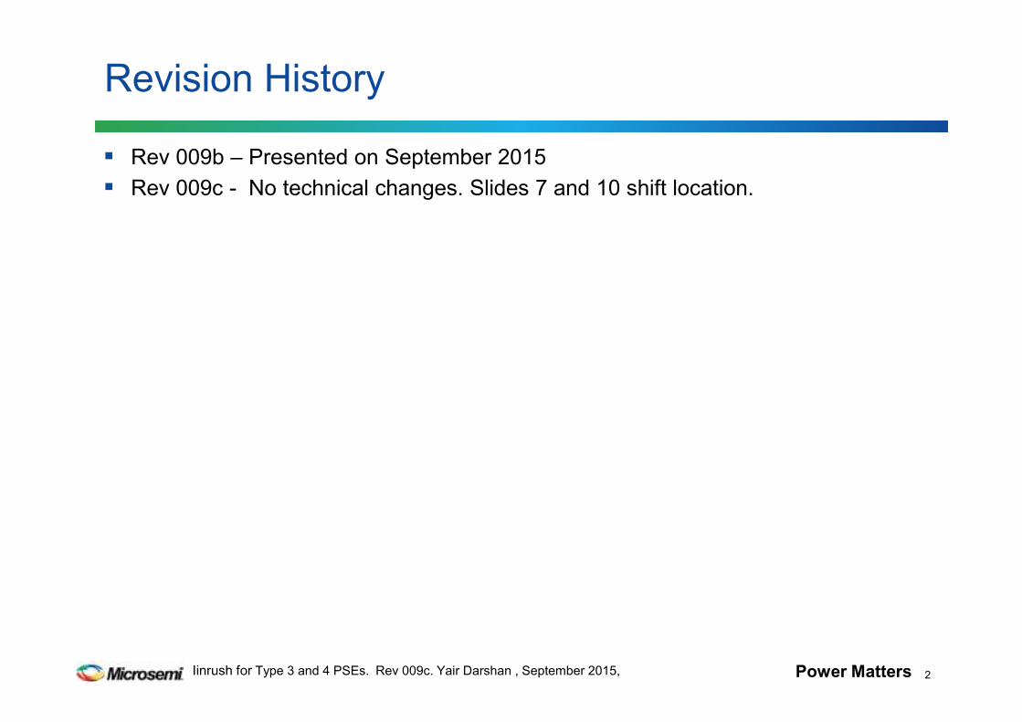
Rev 009b – Presented on September 2015
Rev 009c - No technical changes. Slides 7 and 10 shift location.
Revision History
2
Power MattersIinrush for Type 3 and 4 PSEs. Rev 009c. Yair Darshan , September 2015,
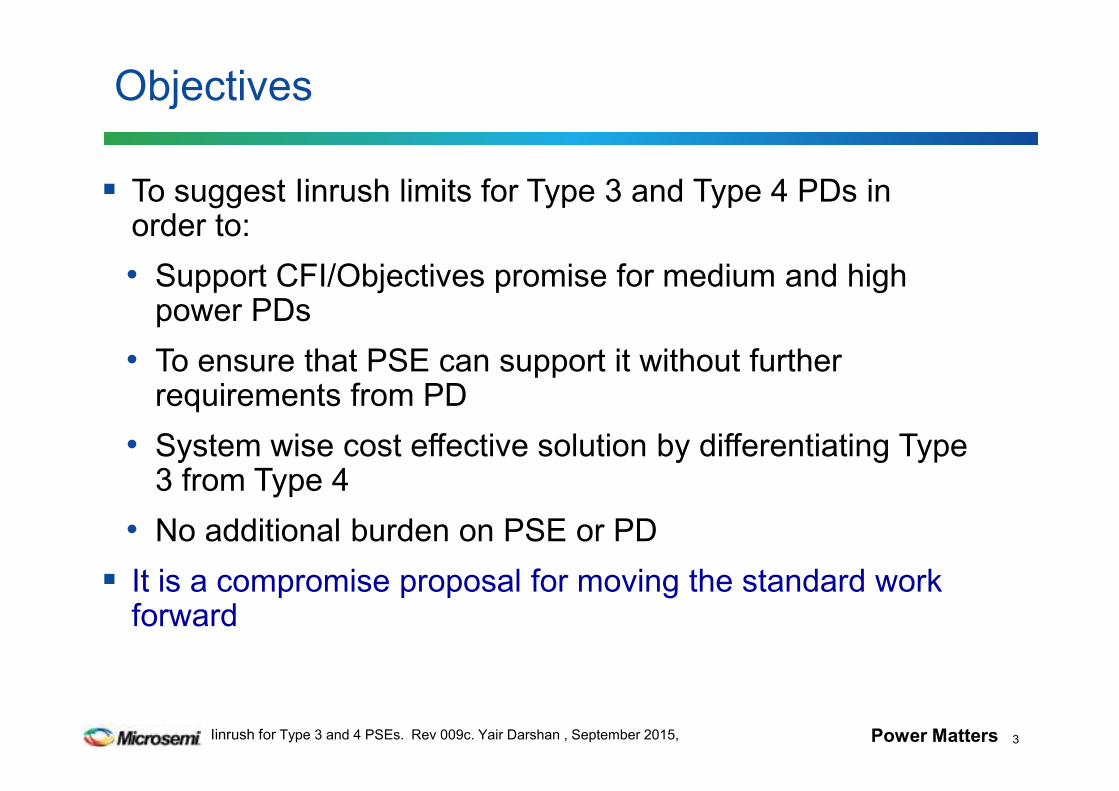
Objectives
To suggest Iinrush limits for Type 3 and Type 4 PDs in order to:
• Support CFI/Objectives promise for medium and high power PDs
• To ensure that PSE can support it without further requirements from PD
• System wise cost effective solution by differentiating Type 3 from Type 4
• No additional burden on PSE or PD
It is a compromise proposal for moving the standard work forward
3
Power MattersIinrush for Type 3 and 4 PSEs. Rev 009c. Yair Darshan , September 2015,
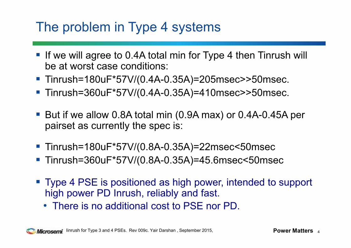
If we will agree to 0.4A total min for Type 4 then Tinrush will be at worst case conditions:
Tinrush=180uF*57V/(0.4A-0.35A)=205msec>>50msec.
Tinrush=360uF*57V/(0.4A-0.35A)=410msec>>50msec.
But if we allow 0.8A total min (0.9A max) or 0.4A-0.45A per pairset as currently the spec is:
Tinrush=180uF*57V/(0.8A-0.35A)=22msec<50msec
Tinrush=360uF*57V/(0.8A-0.35A)=45.6msec<50msec
Type 4 PSE is positioned as high power, intended to support high power PD Inrush, reliably and fast.
• There is no additional cost to PSE nor PD.
The problem in Type 4 systems
4
Power MattersIinrush for Type 3 and 4 PSEs. Rev 009c. Yair Darshan , September 2015,
Proposal Summary
# Parameter Symbol Units Min Max PSE Type
Additional Information
5 Output current
in POWER_UP
state
Iinrush A 0.4 See
Info
1,2,3,
4
For Type 1 and Type 2 PDs.
See 33.2.7.5. Max value defined by Figure 33-13.
5a Output current
per pairset in
POWER_UP
state
Iinrush-2P A 0.2 See
Info
3 For class 5-6 PDs.
Optionally, for both pairsets, total Iinrush is 0.4A
minimum, 0.9A maximum.
See 33.2.7.5. Max value defined by Figure 33-13.
5a
5b
Output current
per pairset in
POWER_UP
state
Iinrush-2P A 0.4 See
Info
4 For class 7-8 PDs.
See 33.2.7.5. Max value defined by Figure 33-13.
Optionally for both pairsets, total Iinrush is 0.8A
minimum, 0.9A maximum.
5
To update the text in 33.3.7.3 to reflect that the Cport which PSE is
responsible to limit Iinrush-2P per the following:
For Type 1-3 PSE all classes: 180uF for SS PD.
For Type 4 PSE classes 7-8: 360uF for SS PD.
See also slide 7 next slide for addressing Cport
Power MattersIinrush for Type 3 and 4 PSEs. Rev 009c. Yair Darshan , September 2015,
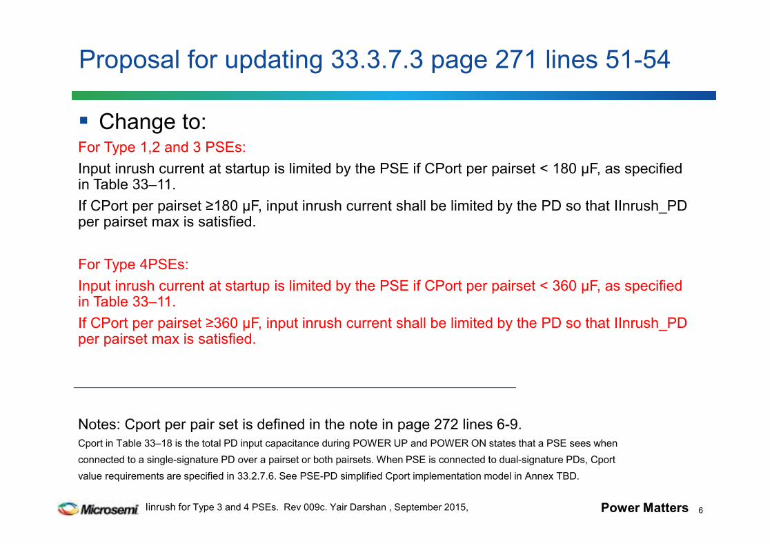
Proposal for updating 33.3.7.3 page 271 lines 51-54
Change to:For Type 1,2 and 3 PSEs:
Input inrush current at startup is limited by the PSE if CPort per pairset < 180 µF, as specified in Table 33–11.
If CPort per pairset ≥180 µF, input inrush current shall be limited by the PD so that IInrush_PDper pairset max is satisfied.
For Type 4PSEs:
Input inrush current at startup is limited by the PSE if CPort per pairset < 360 µF, as specified in Table 33–11.
If CPort per pairset ≥360 µF, input inrush current shall be limited by the PD so that IInrush_PDper pairset max is satisfied.
Notes: Cport per pair set is defined in the note in page 272 lines 6-9.
Cport in Table 33–18 is the total PD input capacitance during POWER UP and POWER ON states that a PSE sees when
connected to a single-signature PD over a pairset or both pairsets. When PSE is connected to dual-signature PDs, Cport
value requirements are specified in 33.2.7.6. See PSE-PD simplified Cport implementation model in Annex TBD.
6
Power MattersIinrush for Type 3 and 4 PSEs. Rev 009c. Yair Darshan , September 2015,
Discussion
7

Power MattersIinrush for Type 3 and 4 PSEs. Rev 009c. Yair Darshan , September 2015, 8
Thank YouAdditional Information are presented in the Annexes next
Power MattersIinrush for Type 3 and 4 PSEs. Rev 009c. Yair Darshan , September 2015,
Backup Slides
9
Power MattersIinrush for Type 3 and 4 PSEs. Rev 009c. Yair Darshan , September 2015,
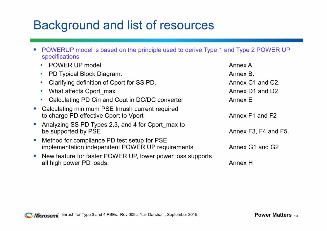
Background and list of resources
POWERUP model is based on the principle used to derive Type 1 and Type 2 POWER UP specifications
• POWER UP model: Annex A.
• PD Typical Block Diagram: Annex B.
• Clarifying definition of Cport for SS PD. Annex C1 and C2.
• What affects Cport_max Annex D1 and D2.
• Calculating PD Cin and Cout in DC/DC converter Annex E
Calculating minimum PSE Inrush current required to charge PD effective Cport to Vport Annex F1 and F2
Analyzing SS PD Types 2,3, and 4 for Cport_max to be supported by PSE Annex F3, F4 and F5.
Method for compliance PD test setup for PSE implementation independent POWER UP requirements Annex G1 and G2
New feature for faster POWER UP, lower power loss supportsall high power PD loads. Annex H
10
Power MattersIinrush for Type 3 and 4 PSEs. Rev 009c. Yair Darshan , September 2015,
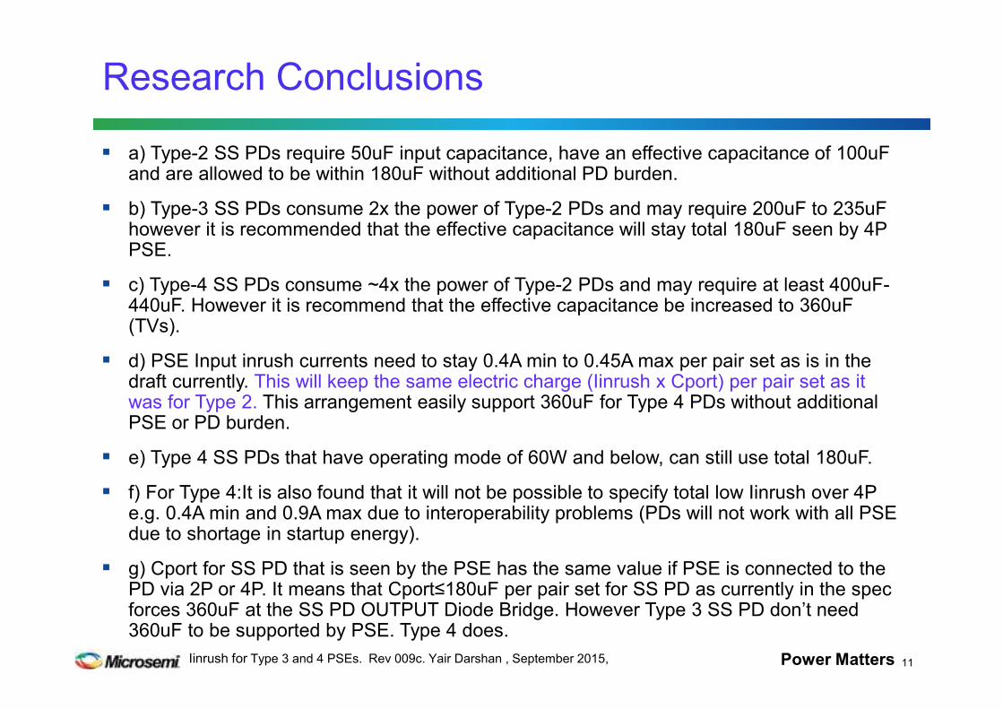
a) Type-2 SS PDs require 50uF input capacitance, have an effective capacitance of 100uF and are allowed to be within 180uF without additional PD burden.
b) Type-3 SS PDs consume 2x the power of Type-2 PDs and may require 200uF to 235uF however it is recommended that the effective capacitance will stay total 180uF seen by 4P PSE.
c) Type-4 SS PDs consume ~4x the power of Type-2 PDs and may require at least 400uF-440uF. However it is recommend that the effective capacitance be increased to 360uF (TVs).
d) PSE Input inrush currents need to stay 0.4A min to 0.45A max per pair set as is in the draft currently. This will keep the same electric charge (Iinrush x Cport) per pair set as it was for Type 2. This arrangement easily support 360uF for Type 4 PDs without additional PSE or PD burden.
e) Type 4 SS PDs that have operating mode of 60W and below, can still use total 180uF.
f) For Type 4:It is also found that it will not be possible to specify total low Iinrush over 4P e.g. 0.4A min and 0.9A max due to interoperability problems (PDs will not work with all PSE due to shortage in startup energy).
g) Cport for SS PD that is seen by the PSE has the same value if PSE is connected to the PD via 2P or 4P. It means that Cport≤180uF per pair set for SS PD as currently in the spec forces 360uF at the SS PD OUTPUT Diode Bridge. However Type 3 SS PD don’t need 360uF to be supported by PSE. Type 4 does.
Research Conclusions
11
Power MattersIinrush for Type 3 and 4 PSEs. Rev 009c. Yair Darshan , September 2015,
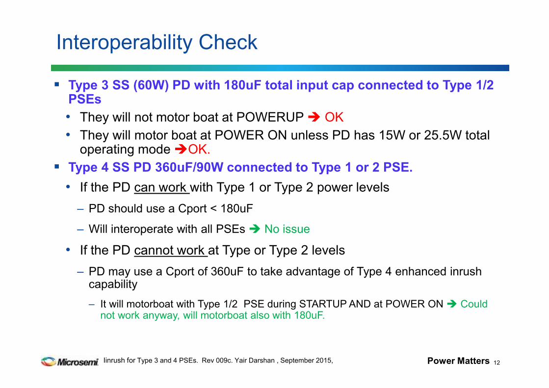
Interoperability Check
Type 3 SS (60W) PD with 180uF total input cap connected to Type 1/2 PSEs
• They will not motor boat at POWERUP OK
• They will motor boat at POWER ON unless PD has 15W or 25.5W total operating mode OK.
Type 4 SS PD 360uF/90W connected to Type 1 or 2 PSE.
• If the PD can work with Type 1 or Type 2 power levels
– PD should use a Cport < 180uF
– Will interoperate with all PSEs No issue
• If the PD cannot work at Type or Type 2 levels
– PD may use a Cport of 360uF to take advantage of Type 4 enhanced inrush capability
– It will motorboat with Type 1/2 PSE during STARTUP AND at POWER ON Could not work anyway, will motorboat also with 180uF.
12
Power MattersIinrush for Type 3 and 4 PSEs. Rev 009c. Yair Darshan , September 2015,
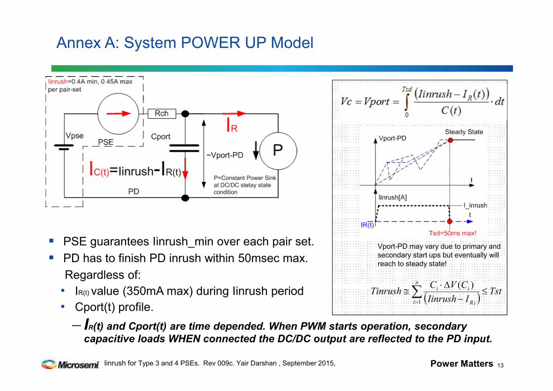
Annex A: System POWER UP Model
PSE guarantees Iinrush_min over each pair set.
PD has to finish PD inrush within 50msec max.
Regardless of:
• IR(t) value (350mA max) during Iinrush period
• Cport(t) profile.
– IR(t) and Cport(t) are time depended. When PWM starts operation, secondary
capacitive loads WHEN connected the DC/DC output are reflected to the PD input.
13
Vport-PD may vary due to primary and
secondary start ups but eventually will
reach to steady state!
( ) TstIIinrush
CVCTinrush
n
i iR
ii ≤−
∆⋅≅∑
=1
)(
Power MattersIinrush for Type 3 and 4 PSEs. Rev 009c. Yair Darshan , September 2015,
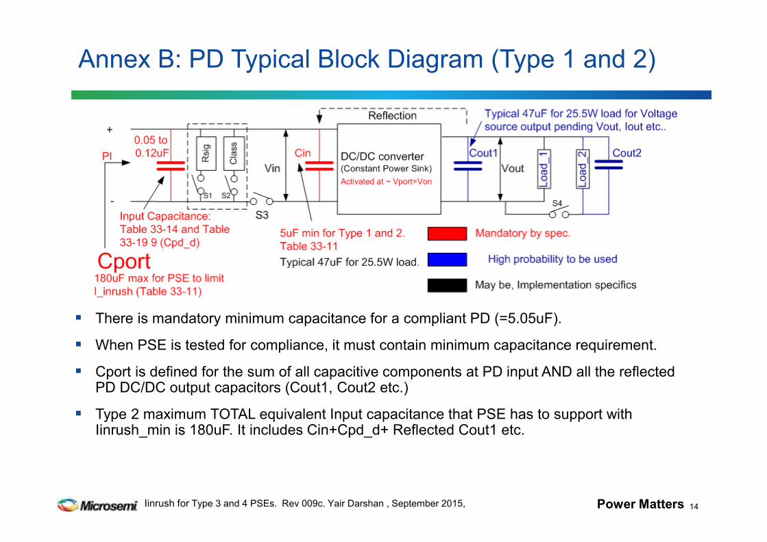
Annex B: PD Typical Block Diagram (Type 1 and 2)
There is mandatory minimum capacitance for a compliant PD (=5.05uF).
When PSE is tested for compliance, it must contain minimum capacitance requirement.
Cport is defined for the sum of all capacitive components at PD input AND all the reflected PD DC/DC output capacitors (Cout1, Cout2 etc.)
Type 2 maximum TOTAL equivalent Input capacitance that PSE has to support with Iinrush_min is 180uF. It includes Cin+Cpd_d+ Reflected Cout1 etc.
14
Power MattersIinrush for Type 3 and 4 PSEs. Rev 009c. Yair Darshan , September 2015,
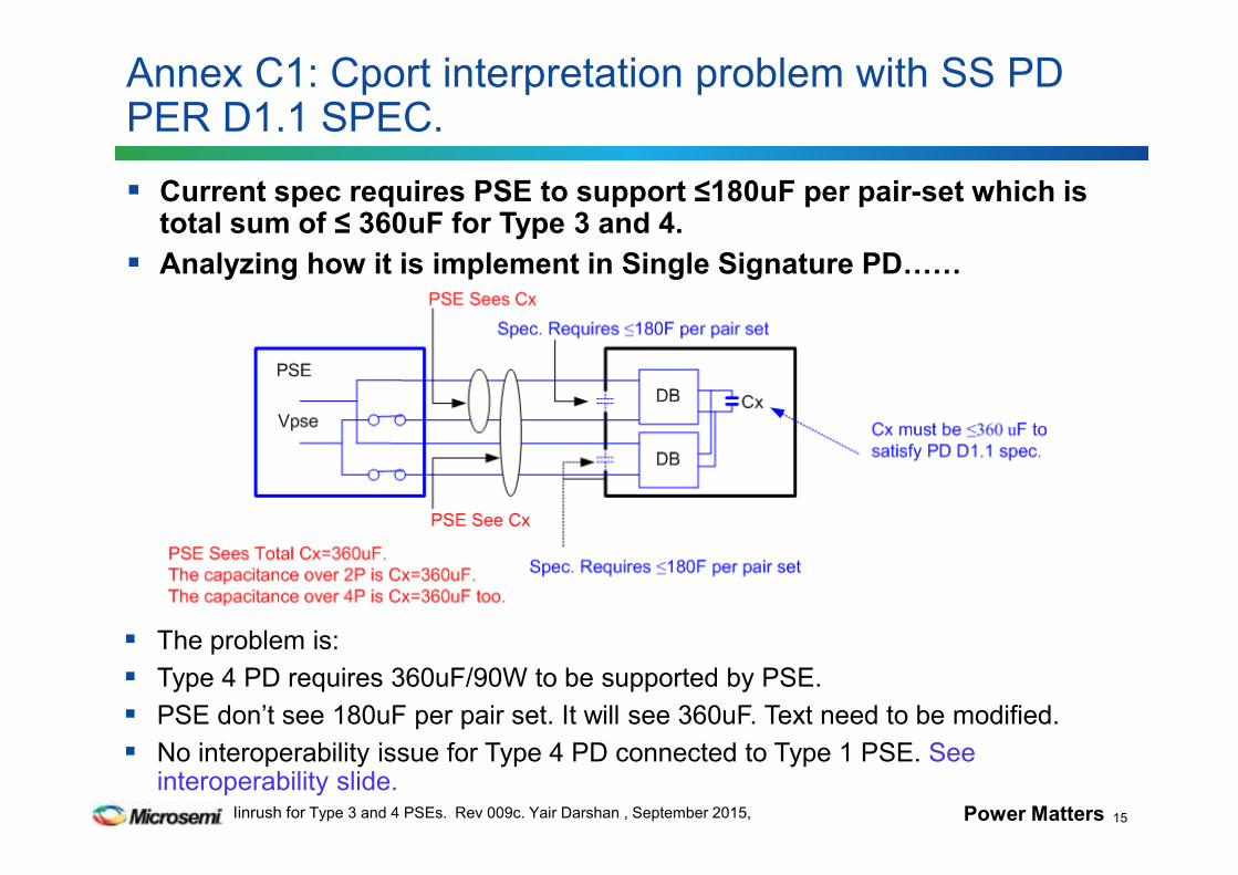
Annex C1: Cport interpretation problem with SS PD PER D1.1 SPEC.
The problem is:
Type 4 PD requires 360uF/90W to be supported by PSE.
PSE don’t see 180uF per pair set. It will see 360uF. Text need to be modified.
No interoperability issue for Type 4 PD connected to Type 1 PSE. See interoperability slide.
15
Current spec requires PSE to support ≤180uF per pair-set which is total sum of ≤ 360uF for Type 3 and 4.
Analyzing how it is implement in Single Signature PD55
Power MattersIinrush for Type 3 and 4 PSEs. Rev 009c. Yair Darshan , September 2015,
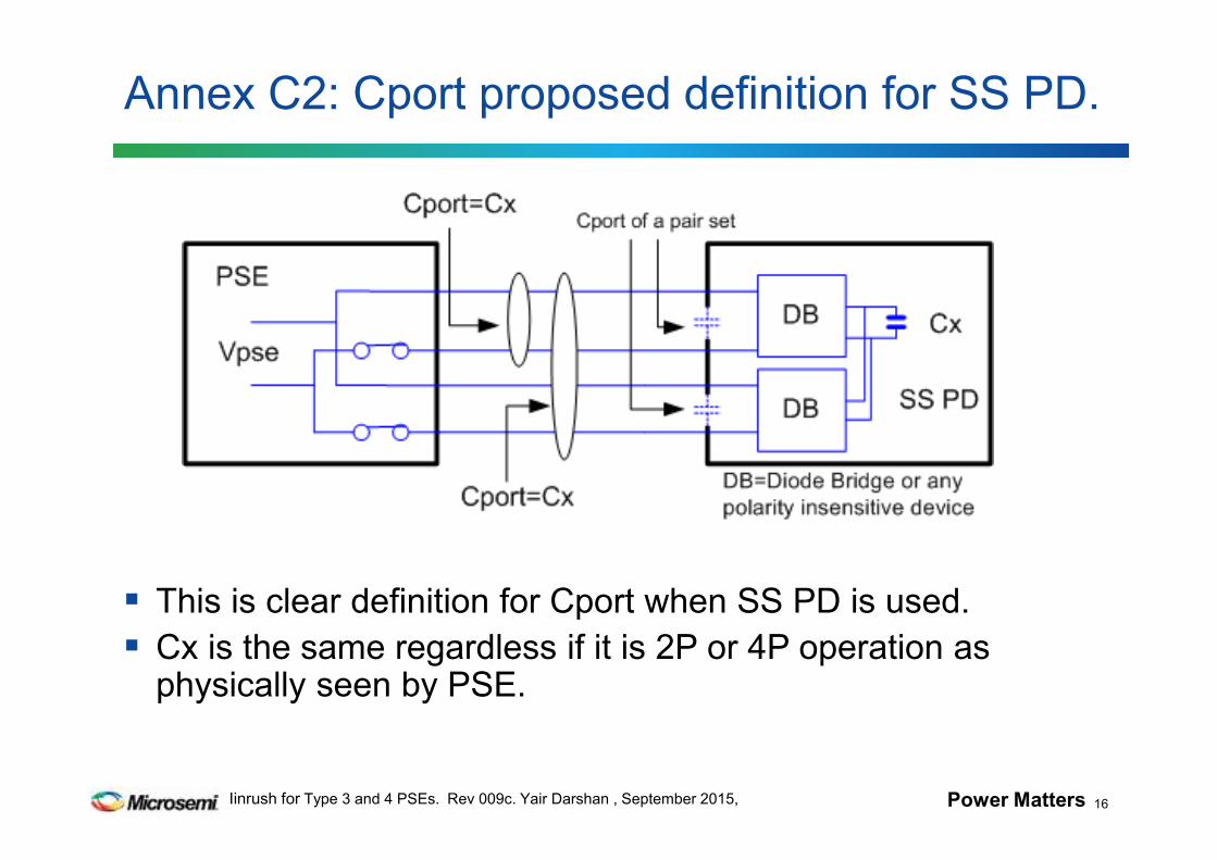
Annex C2: Cport proposed definition for SS PD.
16
This is clear definition for Cport when SS PD is used.
Cx is the same regardless if it is 2P or 4P operation as physically seen by PSE.
Power MattersIinrush for Type 3 and 4 PSEs. Rev 009c. Yair Darshan , September 2015,
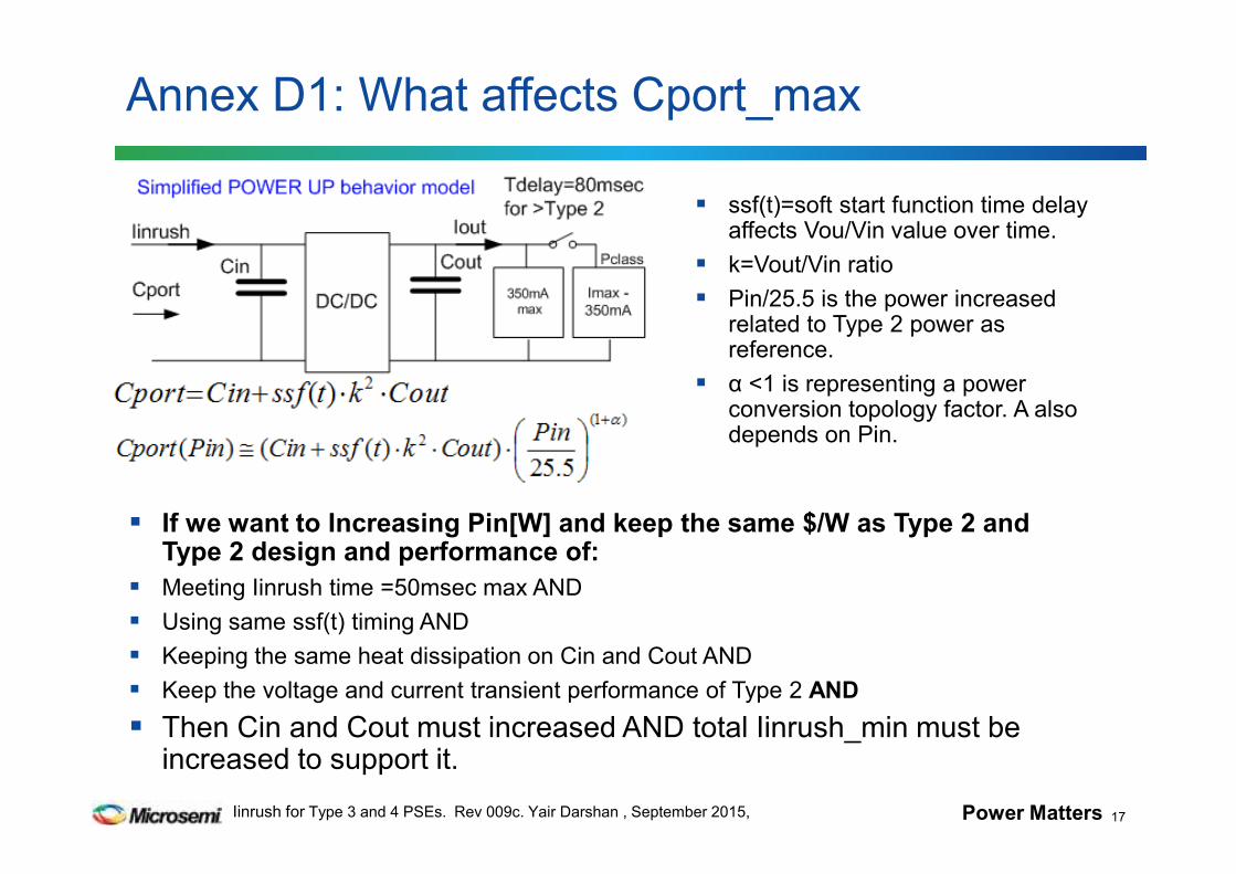
Annex D1: What affects Cport_max
ssf(t)=soft start function time delay affects Vou/Vin value over time.
k=Vout/Vin ratio
Pin/25.5 is the power increased related to Type 2 power as reference.
α <1 is representing a power conversion topology factor. Α also depends on Pin.
17
If we want to Increasing Pin[W] and keep the same $/W as Type 2 and Type 2 design and performance of:
Meeting Iinrush time =50msec max AND
Using same ssf(t) timing AND
Keeping the same heat dissipation on Cin and Cout AND
Keep the voltage and current transient performance of Type 2 AND
Then Cin and Cout must increased AND total Iinrush_min must be increased to support it.
Power MattersIinrush for Type 3 and 4 PSEs. Rev 009c. Yair Darshan , September 2015,
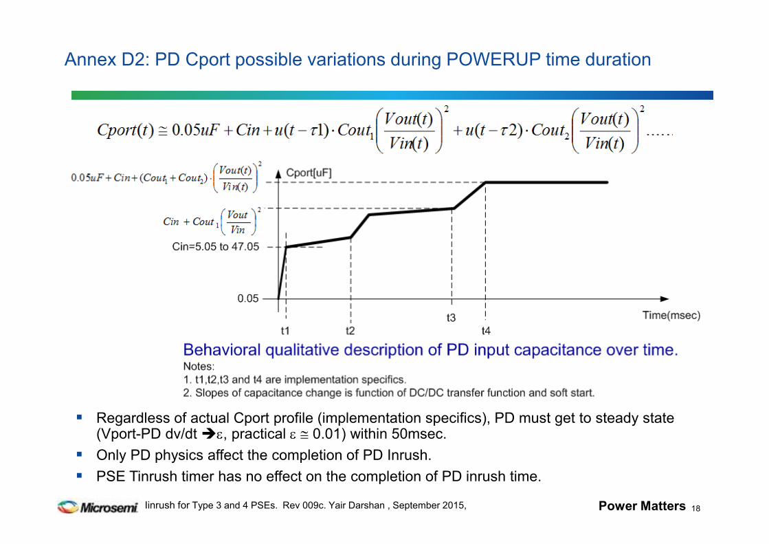
Annex D2: PD Cport possible variations during POWERUP time duration
Regardless of actual Cport profile (implementation specifics), PD must get to steady state (Vport-PD dv/dt ε, practical ε ≅ 0.01) within 50msec.
Only PD physics affect the completion of PD Inrush.
PSE Tinrush timer has no effect on the completion of PD inrush time.
18
Power MattersIinrush for Type 3 and 4 PSEs. Rev 009c. Yair Darshan , September 2015,
Annex E: Calculating PD Cin and Cout in DC/DC converter
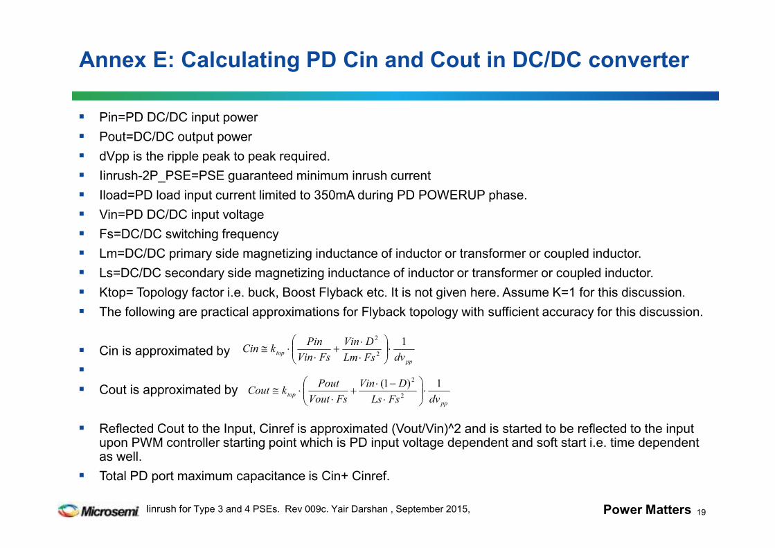
Pin=PD DC/DC input power
Pout=DC/DC output power
dVpp is the ripple peak to peak required.
Iinrush-2P_PSE=PSE guaranteed minimum inrush current
Iload=PD load input current limited to 350mA during PD POWERUP phase.
Vin=PD DC/DC input voltage
Fs=DC/DC switching frequency
Lm=DC/DC primary side magnetizing inductance of inductor or transformer or coupled inductor.
Ls=DC/DC secondary side magnetizing inductance of inductor or transformer or coupled inductor.
Ktop= Topology factor i.e. buck, Boost Flyback etc. It is not given here. Assume K=1 for this discussion.
The following are practical approximations for Flyback topology with sufficient accuracy for this discussion.
Cin is approximated by
Cout is approximated by
Reflected Cout to the Input, Cinref is approximated (Vout/Vin)^2 and is started to be reflected to the input upon PWM controller starting point which is PD input voltage dependent and soft start i.e. time dependent as well.
Total PD port maximum capacitance is Cin+ Cinref.
19
pp
topdvFsLm
DVin
FsVin
PinkCin
12
2
⋅
⋅
⋅+
⋅⋅≅
pp
topdvFsLs
DVin
FsVout
PoutkCout
1)1(2
2
⋅
⋅
−⋅+
⋅⋅≅
Power MattersIinrush for Type 3 and 4 PSEs. Rev 009c. Yair Darshan , September 2015,
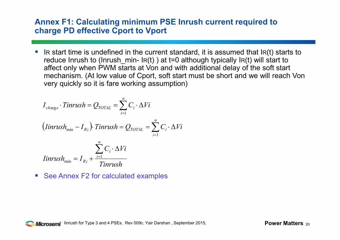
Annex F1: Calculating minimum PSE Inrush current required to charge PD effective Cport to Vport
IR start time is undefined in the current standard, it is assumed that IR(t) starts to reduce Inrush to (Inrush_min- IR(t) ) at t=0 although typically IR(t) will start to affect only when PWM starts at Von and with additional delay of the soft start mechanism. (At low value of Cport, soft start must be short and we will reach Von very quickly so it is fare working assumption)
See Annex F2 for calculated examples
20
( )
Tinrush
ViC
IIinrush
ViCQTinrushIIinrush
ViCQTinrushI
n
i
i
iR
n
i
iTOTALiR
n
i
iTOTALech
∆⋅+=
∆⋅==⋅−
∆⋅==⋅
∑
∑
∑
=
=
=
1min
1
min
1
arg
Power MattersIinrush for Type 3 and 4 PSEs. Rev 009c. Yair Darshan , September 2015,
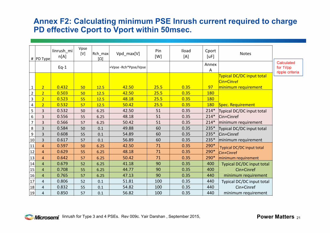
Annex F2: Calculating minimum PSE Inrush current required to charge PD effective Cport to Vport within 50msec.
21
# PD Type
Iinrush_mi
n[A]
Vpse
[V] Rch_max
[Ω]
Vpd_max[V]Pin
[W]
Iload
[A]
Cport
[uF]Notes
Eq-1 =Vpse -Rch*Ppse/VpseAnnex
A
1 2 0.432 50 12.5 42.50 25.5 0.35 97
Typical DC/DC input total
Cin+Cinref
minimum requirement
2 2 0.503 50 12.5 42.50 25.5 0.35 180
Spec. Requirement
3 2 0.523 55 12.5 48.18 25.5 0.35 180
4 2 0.532 57 12.5 50.42 25.5 0.35 180
5 3 0.532 50 6.25 42.50 51 0.35 214* Typical DC/DC input total
Cin+Cinref
minimum requirement
6 3 0.556 55 6.25 48.18 51 0.35 214*
7 3 0.566 57 6.25 50.42 51 0.35 214*
8 3 0.584 50 0.1 49.88 60 0.35 235* Typical DC/DC input total
Cin+Cinref
minimum requirement
9 3 0.608 55 0.1 54.89 60 0.35 235*
10 3 0.617 57 0.1 56.89 60 0.35 235*
11 4 0.597 50 6.25 42.50 71 0.35 290* Typical DC/DC input total
Cin+Cinref
minimum requirement
12 4 0.629 55 6.25 48.18 71 0.35 290*
13 4 0.642 57 6.25 50.42 71 0.35 290*
14 4 0.679 52 6.25 41.18 90 0.35 400 Typical DC/DC input total
Cin+Cinref
minimum requirement
15 4 0.708 55 6.25 44.77 90 0.35 400
16 4 0.765 57 6.25 47.13 90 0.35 440
17 4 0.806 52 0.1 51.81 100 0.35 440 Typical DC/DC input total
Cin+Cinref
minimum requirement
18 4 0.832 55 0.1 54.82 100 0.35 440
19 4 0.850 57 0.1 56.82 100 0.35 440
Calculated
for 1Vpp
ripple criteria
Power MattersIinrush for Type 3 and 4 PSEs. Rev 009c. Yair Darshan , September 2015,
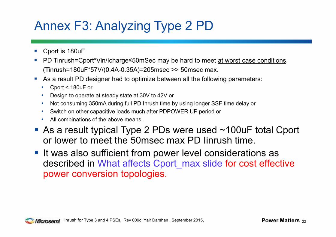
Annex F3: Analyzing Type 2 PD
Cport is 180uF
PD Tinrush=Cport*Vin/Icharge≤50mSec may be hard to meet at worst case conditions.
(Tinrush=180uF*57V/(0.4A-0.35A)=205msec >> 50msec max.
As a result PD designer had to optimize between all the following parameters:
• Cport < 180uF or
• Design to operate at steady state at 30V to 42V or
• Not consuming 350mA during full PD Inrush time by using longer SSF time delay or
• Switch on other capacitive loads much after PDPOWER UP period or
• All combinations of the above means.
As a result typical Type 2 PDs were used ~100uF total Cportor lower to meet the 50msec max PD Iinrush time.
It was also sufficient from power level considerations as described in What affects Cport_max slide for cost effective power conversion topologies.
22
Power MattersIinrush for Type 3 and 4 PSEs. Rev 009c. Yair Darshan , September 2015,
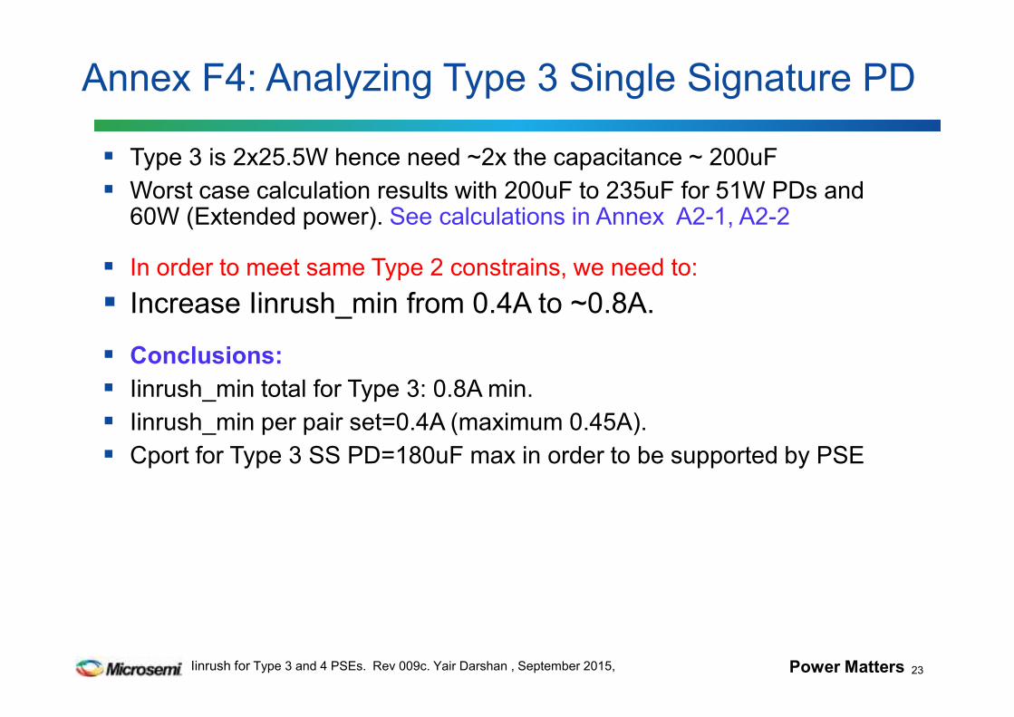
Annex F4: Analyzing Type 3 Single Signature PD
Type 3 is 2x25.5W hence need ~2x the capacitance ~ 200uF
Worst case calculation results with 200uF to 235uF for 51W PDs and 60W (Extended power). See calculations in Annex A2-1, A2-2
In order to meet same Type 2 constrains, we need to:
Increase Iinrush_min from 0.4A to ~0.8A.
Conclusions:
Iinrush_min total for Type 3: 0.8A min.
Iinrush_min per pair set=0.4A (maximum 0.45A).
Cport for Type 3 SS PD=180uF max in order to be supported by PSE
23
Power MattersIinrush for Type 3 and 4 PSEs. Rev 009c. Yair Darshan , September 2015,
Annex F5: Analyzing Type 3 Single Signature PD
Type 4 is ~4X Type 2 Power hence needs 400uF to 440uF for 71W PDs and 90W (Extended power).
We can reduce it to 360uF if and only if Iinrus_min total =0.8A min.• (Allows some flexibility)
See calculations in Annex A2-1, A2-2.
Conclusions:
Iinrush_min for Type 4: 0.8A min.
Iinrush_min per pair set=0.4A (maximum 0.45A).
Cport for Type 4 SS PD=360uF max in order to be supported by PSE.
24
Power MattersIinrush for Type 3 and 4 PSEs. Rev 009c. Yair Darshan , September 2015,
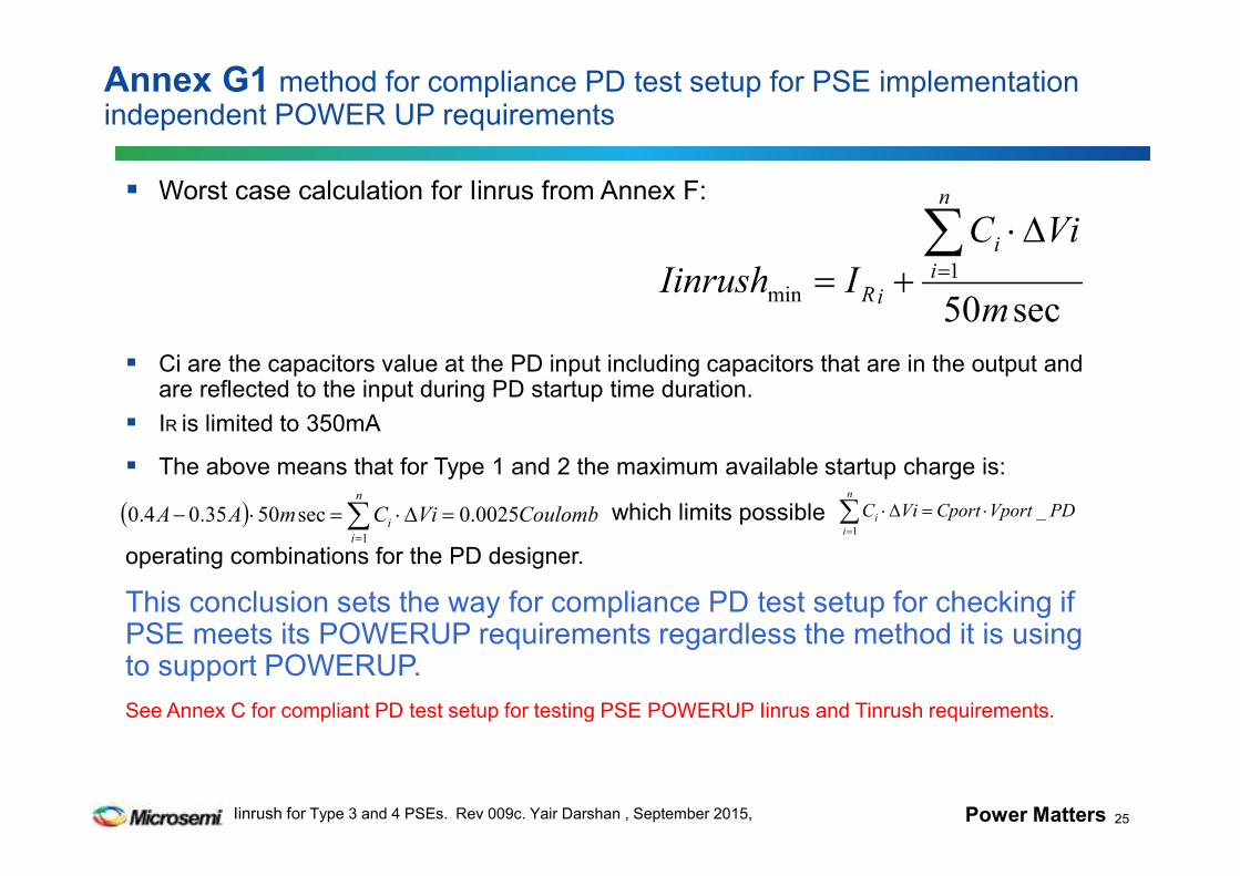
Annex G1 method for compliance PD test setup for PSE implementation independent POWER UP requirements
Worst case calculation for Iinrus from Annex F:
Ci are the capacitors value at the PD input including capacitors that are in the output and are reflected to the input during PD startup time duration.
IR is limited to 350mA
The above means that for Type 1 and 2 the maximum available startup charge is:
which limits possible
operating combinations for the PD designer.
This conclusion sets the way for compliance PD test setup for checking if PSE meets its POWERUP requirements regardless the method it is using to support POWERUP.
See Annex C for compliant PD test setup for testing PSE POWERUP Iinrus and Tinrush requirements.
25
sec50
1min
m
ViC
IIinrush
n
i
i
iR
∆⋅+=∑=
( ) CoulombViCmAAn
i
i 0025.0sec5035.04.01
=∆⋅=⋅− ∑=
PDVportCportViCn
i
i _1
⋅=∆⋅∑=
Power MattersIinrush for Type 3 and 4 PSEs. Rev 009c. Yair Darshan , September 2015,
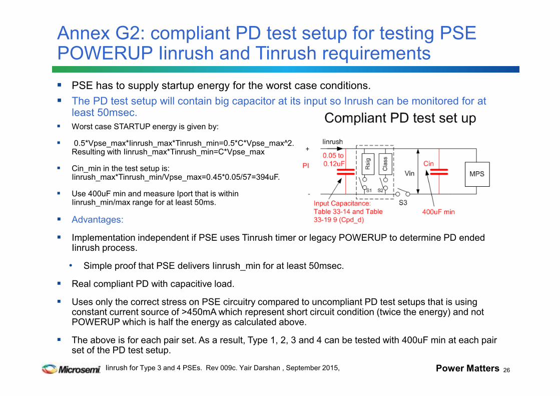
Annex G2: compliant PD test setup for testing PSE POWERUP Iinrush and Tinrush requirements
26
PSE has to supply startup energy for the worst case conditions.
The PD test setup will contain big capacitor at its input so Inrush can be monitored for at least 50msec.
Worst case STARTUP energy is given by:
0.5*Vpse_max*Iinrush_max*Tinrush_min=0.5*C*Vpse_max^2. Resulting with Iinrush_max*Tinrush_min=C*Vpse_max
Cin_min in the test setup is: Iinrush_max*Tinrush_min/Vpse_max=0.45*0.05/57=394uF.
Use 400uF min and measure Iport that is within Iinrush_min/max range for at least 50ms.
Advantages:
Implementation independent if PSE uses Tinrush timer or legacy POWERUP to determine PD ended Iinrush process.
• Simple proof that PSE delivers Iinrush_min for at least 50msec.
Real compliant PD with capacitive load.
Uses only the correct stress on PSE circuitry compared to uncompliant PD test setups that is using constant current source of >450mA which represent short circuit condition (twice the energy) and not POWERUP which is half the energy as calculated above.
The above is for each pair set. As a result, Type 1, 2, 3 and 4 can be tested with 400uF min at each pair set of the PD test setup.
Power MattersIinrush for Type 3 and 4 PSEs. Rev 009c. Yair Darshan , September 2015,
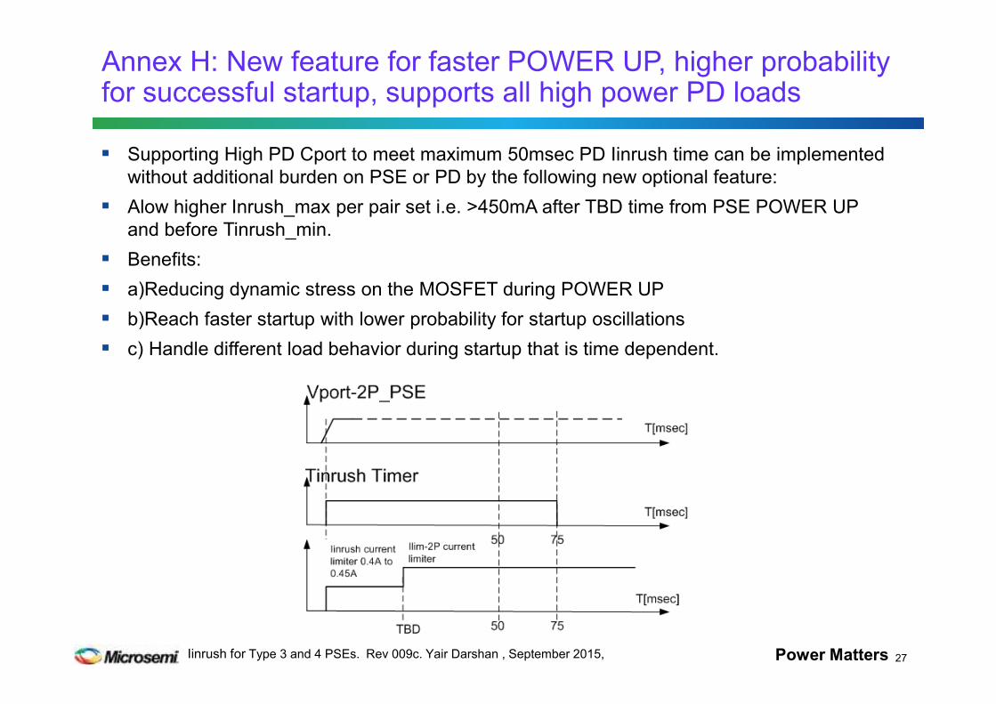
Supporting High PD Cport to meet maximum 50msec PD Iinrush time can be implemented
without additional burden on PSE or PD by the following new optional feature:
Alow higher Inrush_max per pair set i.e. >450mA after TBD time from PSE POWER UP
and before Tinrush_min.
Benefits:
a)Reducing dynamic stress on the MOSFET during POWER UP
b)Reach faster startup with lower probability for startup oscillations
c) Handle different load behavior during startup that is time dependent.
Annex H: New feature for faster POWER UP, higher probability for successful startup, supports all high power PD loads
27