Embed Size (px)
Citation preview

University of Arkansas, FayettevilleScholarWorks@UARKElectrical Engineering Undergraduate HonorsTheses Electrical Engineering
5-2015
Implementation of Natural Switching SurfaceControl for a Flyback ConverterEthan Storm WilliamsUniversity of Arkansas, Fayetteville
Follow this and additional works at: http://scholarworks.uark.edu/eleguht
Part of the Power and Energy Commons, and the VLSI and Circuits, Embedded and HardwareSystems Commons
This Thesis is brought to you for free and open access by the Electrical Engineering at ScholarWorks@UARK. It has been accepted for inclusion inElectrical Engineering Undergraduate Honors Theses by an authorized administrator of ScholarWorks@UARK. For more information, please [email protected], [email protected].
Recommended CitationWilliams, Ethan Storm, "Implementation of Natural Switching Surface Control for a Flyback Converter" (2015). Electrical EngineeringUndergraduate Honors Theses. 41.http://scholarworks.uark.edu/eleguht/41

Implementation of Natural Switching Surface Control for a Flyback Converter
An Undergraduate Honors College Thesis
in the
Department of Electrical Engineering
College of Engineering
University of Arkansas
Fayetteville, AR
by
Ethan Williams


Abstract
The flyback converter is an extremely common topology used for DC/DC power conversion.
Widely used methods to control the flyback converter include voltage mode and current mode
controllers [1]-[5]. More recently, sliding mode control has been developed for the flyback
converter [6]-[7]. While these control methods may be considered adequate, the Natural
Switching Surface (NSS) sliding mode control method detailed in this thesis presents a more
robust controller. NSS control eliminates the effects presented from variations in components
and design as well as minimizes the effects from external disturbances [6]-[9].
This thesis steps through the complete design and implementation process of a NSS controller
for a 100W flyback converter. The fundamental operational principals of the flyback converter
will be described first. A detailed derivation of the NSS control for a flyback converter will
follow. Simulations of the derived controller will be evaluated in MATLAB/Simulink©
. The
component level selection and design is detailed. Finally, the completed flyback with the NSS
controller is fully tested in a laboratory setting and experimental results are analyzed.

Acknowledgments
Over the past three years, Dr. Balda has provided me the opportunity to work in his research
group at University of Arkansas. I’ve had the privilege to gain real world, hands on design
experiences that will continue to allow me to excel in the Electrical Engineering field and be
ahead of the learning curve. I’m very grateful for the opportunities I have been given. In
addition, I’m thankful for the guidance and friendship that Luciano Andrés García Rodríguez has
given me over the past three years on the various projects we have worked on together. I’d also
like to acknowledge and thank Robert Saunders for the various input and design considerations
he provided for this project. Lastly, I’d like to acknowledge all my Electrical Engineering
friends that were right beside me when the design got tough and were always there to cheer me
up and keep me going.

Dedication
This thesis and all the work associated with it is dedicated to three people: God, my wife, and my
parents. First, God has blessed me with the opportunity to come to University of Arkansas and
have the rare opportunity to find my life’s passion immediately out of high school. I’ve been so
blessed over my college career and have felt the grace and presence of God though this whole
project. Through my struggles, I’ve had the opportunity to grow stronger in my faith. Second,
words cannot explain the appreciation I have for my wife, Kendra Williams. This senior year
has challenged our first year of marriage, but I couldn’t have asked for anyone better to go
through life with. The understanding and comfort you provided me is beyond any expectation I
could have set. All this hard work has been to advance our future, so this project is dedicated to
her. Lastly, this project is also dedicated to my parents. Growing up, they have been nothing but
encouraging and loving. I wouldn’t be who I am or where I am with their help.

Table of Contents
I. Introduction ................................................................................................................................. 1
1.1 Overview ............................................................................................................................... 1
1.2 Organization of Thesis .......................................................................................................... 4
II. Flyback Converter Operation ..................................................................................................... 5
2.1 Components and Operation Principle ................................................................................... 5
2.2 On-State Equations ............................................................................................................... 7
2.3 Off-State Equations ............................................................................................................... 7
2.2 Continuous, Boundary, and Discontinuous Modes of Operation ......................................... 8
2.3 Ideal Flyback Converter Waveforms for BCM .................................................................. 10
III. Natural Switching Surface (NSS) Derivation ......................................................................... 11
3.1 Normalization Equations .................................................................................................... 11
3.2 Normalization and Trajectory of On-State Equations ........................................................ 16
3.3 Normalization and Trajectory of Off-State Equations ........................................................ 18
3.4 Summary of the Normalizing Equations and Normalized Trajectories .............................. 22
IV. Proposed Control Law and Simulations ................................................................................. 24
4.1 Graphical Analysis of the NSS Trajectories ....................................................................... 24
4.2 BCM Trajectories................................................................................................................ 27
4.3 Steady-State BCM Control Law ......................................................................................... 29
4.4 Steady-State Switching Frequency Derivation ................................................................... 32

4.5 Simulations of Steady-State BCM Control Law ................................................................. 34
4.6 Transient Response of BCM Control Law.......................................................................... 39
4.7 Start-Up Operation and Max Input Current Protection....................................................... 42
4.8 Review of Proposed Control ............................................................................................... 50
V. Hardware Design and Component Selection ........................................................................... 52
5.1 Overview and Hardware Design Considerations ................................................................ 52
5.2 Basic Flyback Components and Snubbers .......................................................................... 53
5.3 MOSFET and Gate Driver .................................................................................................. 54
5.4 Input Voltage Feedback ...................................................................................................... 55
5.5 Output Voltage Feedback ................................................................................................... 56
5.6 Primary, Secondary, and Output Current Feedback ........................................................... 57
5.7 Power Supplies.................................................................................................................... 59
5.8 Digital Signal Processor ...................................................................................................... 60
5.9 Photo of Developed Board .................................................................................................. 60
VI. DSP Software Design ............................................................................................................. 63
6.1 Overview of Code Development ........................................................................................ 63
6.2 Oscillator, Interrupt, and GPIO Setup................................................................................. 64
6.3 Timer0 Setup ....................................................................................................................... 65
6.4 ADC Configuration and Interrupt ....................................................................................... 67
6.5 Main Loop and NSS Control .............................................................................................. 69
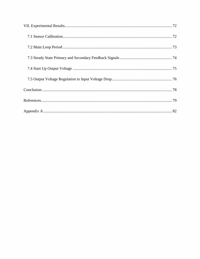
VII. Experimental Results ............................................................................................................. 72
7.1 Sensor Calibration ............................................................................................................... 72
7.2 Main Loop Period ............................................................................................................... 73
7.3 Steady State Primary and Secondary Feedback Signals ..................................................... 74
7.4 Start Up Output Voltage ..................................................................................................... 75
7.5 Output Voltage Regulation to Input Voltage Drop ............................................................. 76
Conclusion .................................................................................................................................... 78
References ..................................................................................................................................... 79
Appendix A ................................................................................................................................... 82

List of Figures
Figure 1: Basic Flyback Converter Topology ................................................................................. 2
Figure 2: Detailed Flyback Converter ............................................................................................. 6
Figure 3: Qon Equivalent Circuit ..................................................................................................... 6
Figure 4: Qoff Equivalent Circuit..................................................................................................... 6
Figure 5: Flyback Modes of Operation ........................................................................................... 9
Figure 6: Ideal Flyback Converter Waveforms for BCM Operation ............................................ 10
Figure 7: Output Filter During Off State ...................................................................................... 13
Figure 8: Generic NSS Graph ....................................................................................................... 24
Figure 9: NSS Trajectory Sliding Direction ................................................................................. 25
Figure 10: NSS Trajectories and Modes of Operation.................................................................. 27
Figure 11: BCM Control Law Trajectories ................................................................................... 30
Figure 12: BCM Control Law Flow Diagram............................................................................... 30
Figure 13: Hypothetical Chattering Situation ............................................................................... 31
Figure 14: Top Level Hierarchy of Simulink©
Flyback Implementation ..................................... 35
Figure 15: Normalized Flyback Equations Simulink©
Block ....................................................... 36
Figure 16: Experimental and Simulation Device Parameters ....................................................... 37
Figure 17: MATLAB Source Code for Steady-State Simulation ................................................ 37
Figure 18: Simulink©
Steady-State Simulation of Trajectories .................................................... 38
Figure 19: Simulink©
Steady-State Simulation: Ip and Is .............................................................. 39
Figure 20: Simulink©
Steady-State Simulation: Vo ...................................................................... 39
Figure 21: Transient Trajectory: DCM ......................................................................................... 41
Figure 22: Transient Trajectory: BCM ......................................................................................... 41
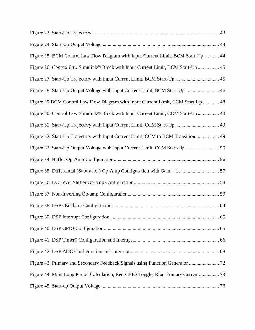
Figure 23: Start-Up Trajectory ...................................................................................................... 43
Figure 24: Start-Up Output Voltage ............................................................................................. 43
Figure 25: BCM Control Law Flow Diagram with Input Current Limit, BCM Start-Up ............ 44
Figure 26: Control Law Simulink© Block with Input Current Limit, BCM Start-Up ................. 45
Figure 27: Start-Up Trajectory with Input Current Limit, BCM Start-Up ................................... 45
Figure 28: Start-Up Output Voltage with Input Current Limit, BCM Start-Up ........................... 46
Figure 29:BCM Control Law Flow Diagram with Input Current Limit, CCM Start-Up ............. 48
Figure 30: Control Law Simulink© Block with Input Current Limit, CCM Start-Up ................. 48
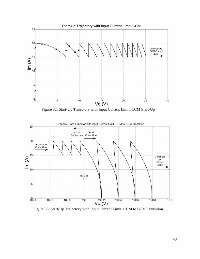
Figure 31: Start-Up Trajectory with Input Current Limit, CCM Start-Up ................................... 49
Figure 32: Start-Up Trajectory with Input Current Limit, CCM to BCM Transition ................... 49
Figure 33: Start-Up Output Voltage with Input Current Limit, CCM Start-Up ........................... 50
Figure 34: Buffer Op-Amp Configuration .................................................................................... 56
Figure 35: Differential (Subtractor) Op-Amp Configuration with Gain = 1 ................................ 57
Figure 36: DC Level Shifter Op-amp Configuration .................................................................... 58
Figure 37: Non-Inverting Op-amp Configuration......................................................................... 59
Figure 38: DSP Oscillator Configuration ..................................................................................... 64
Figure 39: DSP Interrupt Configuration ....................................................................................... 65
Figure 40: DSP GPIO Configuration ............................................................................................ 65
Figure 41: DSP Timer0 Configuration and Interupt ..................................................................... 66
Figure 42: DSP ADC Configuration and Interrupt ....................................................................... 68
Figure 43: Primary and Secondary Feedback Signals using Function Generator ........................ 72
Figure 44: Main Loop Period Calculation, Red-GPIO Toggle, Blue-Primary Current ................ 73
Figure 45: Start-up Output Voltage .............................................................................................. 76

Figure 46: Input Voltage Drop, Red-Input Voltage, Blue-Output Voltage .................................. 77
Figure 47: Main Hierarchical Schematic ...................................................................................... 83

List of Abbreviations
AC – Alternating Current
ADC – Analog-to-Digital Converter
BCM – Boundary Conduction Mode
CCM – Continuous Conduction Mode
DC – Direct Current
DCM – Discontinuous Conduction Mode
DSP – Digital Signal Processor
IC – Integrated Circuit
I/O – Input/Output Pins
MOSFET – Metal-Oxide-Semiconductor Field-Effect Transistor
NSS – Natural Switching Surface
PCB – Printed Circuit Board
RC – Resistor-Capacitor, in Reference to a Snubber Topology
RCD – Resistor-Capacitor-Diode, in reference to a Snubber Topology
Si – Silicon
SiC – Silicon-Carbide
SMC – Sliding Mode Control
SS – Sliding Surface

SSEES – Sustainable Smart Electrical Energy Systems (Research Group of University of
Arkansas)
TI – Texas Instruments
Vgs – Voltage over Gate to Source of MOSFET

1
I. Introduction
1.1 Overview
Switch mode power converters are found everywhere in today’s society. Power electronics are
used in a wide range of applications including computers, cellphones, and power distribution and
generation, to name a few. Through the use of switch mode power converters, voltage or current
can be scaled or modified accordingly to fit the needs of an end application. Switch mode power
converters can be used to convert power to or from DC/AC or be used to convert DC/DC or
AC/AC. A prime example of this conversion need is a cellphone charger. A typical United State
household wall receptacle is 120V AC. Typical cellphone batteries require between 5V to 12V
DC to charge. A switch mode power converter can be implemented in the cellphone charger that
will converter the input AC power to DC power then step the voltage down to the needed DC
voltage level. Ideally, this conversion should be done in the most efficient way with the smallest
packaging and as cheap as possible.
There are multiple different switch mode power converter topology options. Some common
topologies include buck, boost, buck-boost, SEPIC, cûk, zeta, forward converter, push-pull, and
flyback. Each topology has its benefits and limitations and selection is highly dependent upon
the application. This thesis will focus on the design and control of a flyback converter.
University of Arkansas’ Sustainable Smart Electrical Energy Systems (SSEES) Research Group
has previously analyzed multiple converter topologies for the use in renewal energy, specifically
for the harnessing of solar power in microinverter applications. The flyback converter proved to
be the most suitable candidate for this application based on their criteria [10]. Therefore, to
assist SSEES further in their flyback microinverter applications, this research was performed.

2
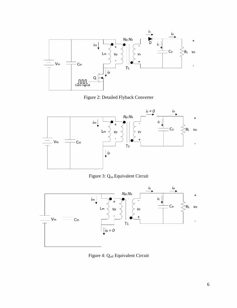
Figure 1: Basic Flyback Converter Topology
The flyback converter is an isolated DC/DC power converter. The use of a flyback transformer
in the topology provides inherent isolation.
Figure 1 shows the basic flyback converter topology. The main components are the input and
output capacitors, Cin and Co respectively, the semiconductor switching device, Q, the flyback
transformer, T1, the output diode, D, and the
load, RL, represented here as purely resistive.

3
The most widely used method to control a traditional flyback converter is current mode control.
Many industries, such as Linear Technologies, Texas Instruments (TI), and ON Semiconductor,
provide integrated circuit (IC) chips that can perform the control function automatically, only
requiring basic feedback signals [1][4][5]. While current mode control may be easy to
implement, it does not necessarily mean that it is the most robust control method. The NSS
control method detailed in this thesis provides many benefits over the traditional current mode
control. NSS control utilizes natural trajectories intrinsically found in the operation of the
flyback converter, making transient times minimal. NSS’s operation is not hindered by
component variations and reacts minimally to external disturbances [8] [9]. In addition, being a
derivative of sliding mode control (SMC), the switching frequency can be ideally infinite if
operating in Continuous Conduction Mode (CCM) to maintain the system on the sliding surface
(SS), creating minimal ripple current in the output [6]. Realistically, infinite switching frequency
is not possible, limited by sensory acquisition and processor calculation times, but nevertheless,
actual NSS control implementation can minimize the current ripple generated.
The flyback converter presented in this thesis was designed for 100W maximum power
conversion, taking an average input of 24V DC and stepping it up to 200V DC. 24V DC was
considered to the normal output voltage of an individual solar panel. 200V DC was chosen to
provided sufficiently high enough voltage for the input stage of a DC/AC inverter for 120V AC
power grid tied microinverter applications. A Silicon (Si) metal-oxide-semiconductor field-
effect transistor (MOSFET) was used as the switching semiconductor device. The flyback
transformer was an off-the-shelf transformer available from Coilcraft, used to minimize

4
development costs. The digital signal processor (DSP) implemented was a Texas Instruments
TMS320F28335.
1.2 Organization of Thesis
This thesis is organized as follows: Chapter 2 details the basic operation of the flyback converter,
detailing governing equations and modes of operation. Chapter 3 provides a detailed derivation
of the Natural Switching Surface (NSS) controller for the flyback converter. Chapter 4 solves
the NSS control for Bound Conduction Mode (BCM) and analyzes the derived controller in
MATLAB/Simulink©
. Chapter 5 details the selection and justification of components for
discrete implementation of the flyback converter and controller. Chapter 6 details the code
developed in the DSP for NSS control implementation. Finally, Chapter 7 analyzes acquired
experimental data from laboratory testing of the NSS controlled flyback converter.

5
II. Flyback Converter Operation
2.1 Components and Operation Principle
Figure 2 shows a detailed version of the flyback converter topology. The main components are
the input and output capacitors, Cin and Co respectively, the semiconductor switching device, Q,
the flyback transformer, T1, the output diode, D, and the load, RL, represented here as purely
resistive. The flyback transformer’s model, T1, has been extended to explicitly show the
magnetizing inductance, Lm, in parallel with an ideal transformer. Our variables of interest, or
state variables, are the output voltage, 𝑣0, and the transformer’s magnetizing current, 𝑖𝑚.
Figure 3 and Figure 4 show the two states for the flyback converter from the switching of Q.
Figure 3 shows the equivalent circuit for when Q is on. Figure 4 shows the equivalent circuit for
when Q is off. In both instances, it is assumed that the on resistance and leakage current of Q
and D is negligible. When Q is on, the input voltage, Vin, is connected in parallel to Lm and Vp
and the primary current, 𝑖𝑝, rises linearly. Therefore, diode D is reverse biased, and no current
flows through the secondary of the transformer. The required load energy is supplied from the
output capacitor, Co. During this on time, energy is stored in T1’s magnetic field. As Q turns
off, the current stops flowing through the primary of T1 and the voltages of Vp and Vs invert
polarity due to Lenz and Faraday law [11]. The diode, D, now becomes forward biased and
allows current to flow to the output, therefore decreasing the energy stored in the magnetic field
of T1. This current recharges the output capacitor, Co, and supplies energy to the load. Since the
output voltage is connected in parallel to the secondary of the transformer, the secondary current,
is, will decrease linearly [12].
6
Figure 2: Detailed Flyback Converter
Figure 3: Qon Equivalent Circuit
Figure 4: Qoff Equivalent Circuit

7
2.2 On-State Equations
During Qon, the primary of the transformer, Vp, is connected in parallel with Vin. The primary
current, ip, is equal to the magnetizing current, im, and is described as
𝑑𝑖𝑚
𝑑𝑡=
𝑉𝑖𝑛
𝐿𝑚 (1)
This can be seen to cause a linear increase in im with an increase in time. The secondary current,
is, is zero during the on time because the diode, D, is reversed biased. The secondary voltage is
related to the primary voltage by the turns ratio.
𝑣𝑠 =𝑁𝑠
𝑁𝑝𝑣𝑝 (2)
The output voltage can be determined by the output capacitor, Co. The output current, io, is
observed to be the negative of the output capacitor current, ic, since is is equal to zero.
𝑑𝑣𝑜
𝑑𝑡= −
𝑖𝑜
𝐶𝑜 (3)
2.3 Off-State Equations
During Qoff, the primary current, ip, is equal to zero since Q blocks the current. The primary and
secondary voltage will flip polarity due T1’s magnetic field decreasing, forcing D to become
forward biased and the secondary current to conduct. The secondary current can be related to the
magnetizing current flowing between the ideal transformer and Lm by the turns ratio.
𝑖𝑠 =𝑁𝑝
𝑁𝑠𝑖𝑚 (4)
The output voltage will be reflected back to the primary by the turns ratio. Note that vo is equal
to -vs.

8
𝑣𝑝 = −𝑣𝑜
𝑁𝑝
𝑁𝑠 (5)
Therefore, Lm’s inductor equation can be written as
−𝑣𝑜
𝑁𝑝
𝑁𝑠= 𝐿𝑚
𝑑𝑖𝑚
𝑑𝑡
𝑑𝑖𝑚
𝑑𝑡=
−𝑣𝑜
𝑁𝑝
𝑁𝑠
𝐿𝑚 (6)
The output voltage is again determined by the output capacitor.
𝑖𝑠 − 𝑖𝑜 = 𝐶𝑜
𝑑𝑣𝑜
𝑑𝑡
𝑑𝑣𝑜
𝑑𝑡=
(𝑁𝑝
𝑁𝑠𝑖𝑚) − 𝑖𝑜
𝐶𝑜 (7)
2.2 Continuous, Boundary, and Discontinuous Modes of Operation
Depending upon the ending value the magnetizing current, im, each switching cycle, the flyback
converter can be classified into three different modes of operation: continuous conduction mode
(CCM), boundary conduction mode (BCM), and discontinuous conduction mode (DCM).
CCM occurs when the magnetic field in the transformer never completely depletes each
switching cycle and therefore the magnetizing current never reaches zero. BCM is classified as
when the magnetizing current reaches zero just as the switch is turned back on. BCM is the
transition between CCM and DCM. DCM occurs when the magnetizing current reaches zero
and stays at zero for the remainder of the switching cycle until Q is turned back on. Figure 5
shows the magnetizing current for all three modes of operation in steady-state.

9
(a) (b) (c)
Figure 5: Flyback Modes of Operation; CCM (a), BCM (b), and CCM (c)
Comparing CCM and DCM applications for the flyback converter, CCM is more appropriate for
constant output voltage situations while DCM is more desirable for constant output current
situations. In DCM and BCM, the flyback converter can react to transients in output load
changes and input voltage swiftly compared to CCM. One downfall of DCM and BCM is larger
currents trough the transformer compared to CCM at the same operating conditions [12]. [13]
performed a detailed analysis for CCM and BCM comparing four major areas of losses:
conduction losses, switching losses, diode losses, and transformer losses. The conclusion was
that a decision of operating mode based solely on losses was not clear due to each mode having
significantly higher and lower losses in different areas. [13] continued with an operational
comparison for CCM and BCM. Ultimately, it was concluded that the benefits of BCM
outweighed CCM. One advantage of BCM was inherent short circuit output protection. Another
significant benefit of BCM is zero current switching for Q at turn on and D at turn off. This
minimizes current spikes associated from Q at turn on and EMI generated from D at turn off
[13]. Therefore, the develop NSS controller will be designed to operate at BCM for all loading
conditions.

10
2.3 Ideal Flyback Converter Waveforms for BCM
Figure 6 details the expected waveforms from an ideal flyback converter operating in BCM in
steady-state operation [12]. These waveforms are a graphical representation of (1)-(7). The duty
cycle is 50% in this representation. The output voltage is represented as a sinusoidal ripple,
though realistically this waveform will differ significantly based off of the output capacitance,
load, duty cycle, and switching frequency.
(a) (d)
(b) (e)
(c) (f)
Figure 6: Ideal Flyback Converter Waveforms for BCM Operation
(a) Magnetizing Current, (b) Primary Current, (c) Secondary Current, (d) Primary Voltage, (e)
Secondary Voltage, and (f) Output Voltage

11
III. Natural Switching Surface (NSS) Derivation
3.1 Normalization Equations
The first step in deriving the natural switching surface for a generic flyback converter is to
normalize the equations that describe the operation of the flyback converter [8]. The trajectories
derived later in the subsections of this chapter are in the 𝑣𝑜𝑛 vs. 𝑖𝑚𝑛 plane. This eliminates the
requirement for converter specific variables and operating conditions and allows for a general
representation of the NSS for any flyback converter. Because the flyback converter involves a
transformer, a reference side must be determined for the normalizing equations. The secondary
side is selected as the reference side. Therefore, 𝑉𝑟, 𝑖𝑟, and 𝑍𝑜 are derived and considered
secondary base variables. (8)(58)(10)(12) and their derivatives (9)(11)(13) detail the equations
used to normalize the flyback converter’s operating equations referred to the secondary side [8]
[14].
𝑣𝑥𝑛 =𝑣𝑥
𝑉𝑟 (8)
𝑑𝑣𝑥𝑛 =𝑑𝑣𝑥
𝑉𝑟 (9)
𝑖𝑥𝑛 =
𝑖𝑥
𝑉𝑟
𝑍𝑜
(10)
𝑑𝑖𝑥𝑛 =
𝑑𝑖𝑥
𝑉𝑟
𝑍𝑜
(11)
𝑡𝑛 =𝑡
𝑇𝑜 (12)
𝑑𝑡𝑛 =𝑑𝑡
𝑇𝑜 (13)
where 𝑣𝑥, 𝑖𝑥, and t are the variables that are to be normalized. It can be observed that 𝑉𝑟
𝑍𝑜 create a
reference current, 𝑖𝑟, which 𝑖𝑥 is normalized against in (10)(11). To normalize a variable that is

12
referred to the primary side, the normalizing base variables must be referred to the primary side.
Reflecting the voltage base from the secondary to the primary requires Vr to be multiplied by 𝑁𝑝
𝑁𝑠.
Reflecting the current base from the secondary to the primary requires 𝑖𝑟 to be multiplied by 𝑁𝑠
𝑁𝑝
[11] [14]. (14)-(17) detail the equations used to normalize the converter specific variables with
the correct base reference.
𝑉𝑖𝑛𝑛 =
𝑉𝑖𝑛
𝑉𝑟
𝑁𝑝
𝑁𝑠
(14)
𝑖𝑚𝑛 =
𝑖𝑚
𝑉𝑟
𝑍𝑜
𝑁𝑠
𝑁𝑝
(15)
𝑣𝑜𝑛 =𝑣𝑜
𝑉𝑟 (16)
𝑖𝑜𝑛 =
𝑖𝑜
𝑉𝑟
𝑍𝑜
(17)
𝑍𝑜 is the characteristic equation of the output filter during the off state. Figure 7 shows the
output filter during the off state, where the secondary inductance, Ls, is equal to Lm, referenced to
the secondary side by the transformer turns ratio [11].
𝐿𝑠 = 𝐿𝑚 (𝑁𝑠
𝑁𝑝)
2
(18)
The characteristic impedance, 𝑍𝑜, can be derived by determining the ratio of the amplitude of the
voltage to the amplitude of the current [15]. Therefore, we must find the equations that describe
the voltage and current. The inductor and capacitor equations are
−𝑣𝑜 = 𝐿𝑚 (𝑁𝑠
𝑁𝑝)
2𝑑𝑖𝑠
𝑑𝑡 (19)

13
Figure 7: Output Filter During Off State
𝑖𝑐 = 𝐶𝑜
𝑑𝑣𝑜
𝑑𝑡 (20)
It can be observed that 𝑖𝑠 = 𝑖𝑐. Solving for the voltage equation first, we can take the derivative
of (20) and substitute the result into (19)
𝑑𝑖𝑠
𝑑𝑡= 𝐶𝑜
𝑑2𝑣𝑜
𝑑𝑡2 (21)
−𝑣0 = 𝐿𝑚 (𝑁𝑠
𝑁𝑝)
2
𝐶𝑜
𝑑2𝑣𝑜
𝑑𝑡2
𝑑2𝑣𝑜
𝑑𝑡2+
𝑣𝑜
𝐿𝑚𝐶𝑜 (𝑁𝑠
𝑁𝑝)
2 = 0 (22)
Solving for this second order differential equation (22), it can be assumed that the general
solution has the form of [15]
𝑣0(𝑡) = 𝐴 ∗ 𝑐𝑜𝑠(𝜔𝑜𝑡 + 𝜑) (23)
where the first and second derivative of (23) equals
𝑑𝑣𝑜
𝑑𝑡= −𝐴𝜔𝑜 ∗ sin(𝜔𝑜𝑡 + 𝜑) (24)
𝑑2𝑣𝑜
𝑑𝑡2= −𝐴𝜔𝑜
2 ∗ cos(𝜔𝑜𝑡 + 𝜑) (25)
Replacing (23) and (25) into (22) results in

14
−𝐴𝜔𝑜
2 ∗ cos(𝜔𝑜𝑡 + 𝜑) +𝐴 ∗ cos(𝜔𝑜𝑡 + 𝜑)
𝐿𝑚𝐶𝑜 (𝑁𝑠
𝑁𝑝)
2 = 0 (26)
Canceling like terms in both add-ins results in a simplified expression for 𝜔𝑜, the natural
frequency [15].
−𝜔𝑜
2 +1
𝐿𝑚𝐶𝑜 (𝑁𝑠
𝑁𝑝)
2 = 0
𝜔𝑜 =
1
𝑁𝑠
𝑁𝑝√𝐿𝑚𝐶𝑜
(27)
The initial conditions of the circuit can be identified from the end of the on-state of the flyback
converter. The secondary current, 𝑖𝑠(0) = 0, and the capacitor voltage can be assumed to be
equal to an arbitrary voltage, 𝑣0(0) = 𝑉𝑎. Plugging into (23), we see that
𝑣0(0) = 𝐴 ∗ cos(𝜑) = 𝑉𝑎 (28)
To eliminate 𝜑, we can look at the initial conditions of (20) and plug in the derivative, (24).
𝑖𝑐(0) = 0 = 𝐶𝑜
𝑑𝑣𝑜
𝑑𝑡
0 = −𝐶𝑜𝐴𝜔𝑜 ∗ sin(𝜑) (29)
Observing both (28) and (29), we can solve for 𝜑. 𝐴 ≠ 0 in (28). Therefore for (29) to be true
𝜑 = 0 (30)
which allows (28) to simplify to
𝐴 = 𝑉𝑎 (31)
Finally, (23) can be completely written as
𝑣0(𝑡) = 𝑉𝑎 cos (1
𝑁𝑠
𝑁𝑝√𝐿𝑚𝐶𝑜
∗ 𝑡) (32)
The current equation, (20), can be completed using the derivative of equation (32).

15
𝑖𝑠(𝑡) = −𝐶0𝑉𝑎
1
𝑁𝑠
𝑁𝑝√𝐿𝑚𝐶𝑜
∗ sin (1
𝑁𝑠
𝑁𝑝√𝐿𝑚𝐶𝑜
∗ 𝑡) (33)
With both the voltage, (32), and current, (33), equations identified, the characteristic equation
can now be computed. Taking the magnitudes of (32) and (33) and plugging into the equation
for Zo [15]
𝑍𝑜 = 𝑣0
𝑖0
𝑍𝑜 =
𝑉𝑎
𝐶0𝑉𝑎1
𝑁𝑠
𝑁𝑝√𝐿𝑚𝐶𝑜
𝑍𝑜 =𝑁𝑠
𝑁𝑝√
𝐿𝑚
𝐶0 (34)
To find 𝑇𝑜 for the normalization of time t, equation (27) can be extended to find 𝑓0 and therefore
𝑇𝑜.
𝜔𝑜 = 2𝜋𝑓𝑜 =
1
𝑁𝑠
𝑁𝑝√𝐿𝑚𝐶𝑜
𝑓𝑜 =
1
2𝜋𝑁𝑠
𝑁𝑝√𝐿𝑚𝐶𝑜
(35)
𝑇𝑜 = 2𝜋𝑁𝑠
𝑁𝑝√𝐿𝑚𝐶𝑜 (36)
To recap this subsection, the variable specific normalizing equations are
𝑉𝑖𝑛𝑛 =
𝑉𝑖𝑛
𝑉𝑟
𝑁𝑝
𝑁𝑠
(14)

16
𝑖𝑚𝑛 =
𝑖𝑚
𝑉𝑟
𝑍𝑜
𝑁𝑠
𝑁𝑝
(15)
𝑣𝑜𝑛 =𝑣𝑜
𝑉𝑟 (16)
𝑖𝑜𝑛 =
𝑖𝑜
𝑉𝑟
𝑍𝑜
(17)
where 𝑣𝑥, 𝑖𝑥, and t are the variables that are to be normalized and
𝑍𝑜 =𝑁𝑠
𝑁𝑝√
𝐿𝑚
𝐶0 (34)
𝑇𝑜 = 2𝜋𝑁𝑠
𝑁𝑝√𝐿𝑚𝐶𝑜 (36)
3.2 Normalization and Trajectory of On-State Equations
The on-state equations were previously defined as
𝑑𝑖𝑚
𝑑𝑡=
𝑉𝑖𝑛
𝐿𝑚 (1)
𝑑𝑣𝑜
𝑑𝑡= −
𝑖𝑜
𝐶𝑜 (3)
Using (14)(15)(16)(17), the on-state equations can be normalized [14]. Starting with (1)
𝑉𝑟
𝑍𝑜
𝑁𝑠
𝑁𝑝(
𝑑𝑖𝑚 𝑉𝑟
𝑍𝑜
𝑁𝑠
𝑁𝑝
)
𝑇𝑜 (𝑑𝑡𝑇𝑜
)=
(𝑉𝑖𝑛
𝑉𝑟
𝑁𝑝
𝑁𝑠
) 𝑉𝑟
𝑁𝑝
𝑁𝑠
𝐿𝑚
𝑉𝑟
𝑍𝑜
𝑁𝑠
𝑁𝑝𝑑𝑖𝑚𝑛
𝑇𝑜 𝑑𝑡𝑛=
𝑉𝑖𝑛𝑛𝑉𝑟
𝑁𝑝
𝑁𝑠
𝐿𝑚
𝑑𝑖𝑚𝑛
𝑑𝑡𝑛= 𝑉𝑖𝑛𝑛
𝑍𝑜𝑇𝑜
𝐿𝑚(
𝑁𝑝
𝑁𝑠)
2

17
𝑑𝑖𝑚𝑛
𝑑𝑡𝑛= 𝑉𝑖𝑛𝑛
𝑁𝑠
𝑁𝑝√
𝐿𝑚
𝐶02𝜋
𝑁𝑠
𝑁𝑝√𝐿𝑚𝐶𝑜
𝐿𝑚(
𝑁𝑝
𝑁𝑠)
2
𝑑𝑖𝑚𝑛
𝑑𝑡𝑛= 𝑉𝑖𝑛𝑛2𝜋 (37)
Continuing with the normalization of (3)
𝑉𝑟 ∗ (𝑑𝑣𝑜
𝑉𝑟)
𝑇𝑜 ∗ (𝑑𝑡𝑇𝑜
)=
− (𝑖𝑜
𝑉𝑟∗ 𝑍𝑜) ∗
𝑉𝑟
𝑍𝑜
𝐶𝑜
𝑉𝑟 ∗ 𝑑𝑣𝑜𝑛
𝑇𝑜 ∗ 𝑑𝑡𝑛=
−𝑖𝑜𝑛 ∗𝑉𝑟
𝑍𝑜
𝐶𝑜
𝑑𝑣𝑜𝑛
𝑑𝑡𝑛= −𝑖𝑜𝑛 ∗
𝑇𝑜
𝑍𝑜𝐶𝑜
𝑑𝑣𝑜𝑛
𝑑𝑡𝑛= −𝑖𝑜𝑛 ∗
2𝜋𝑁𝑠
𝑁𝑝√𝐿𝑚𝐶𝑜
𝐶𝑜𝑁𝑠
𝑁𝑝√
𝐿𝑚
𝐶0
𝑑𝑣𝑜𝑛
𝑑𝑡𝑛= −𝑖𝑜𝑛2𝜋 (38)
To relate (37) and (38) to the 𝑣𝑜𝑛 vs. 𝑖𝑚𝑛 plane, it can be observed that dividing the two
equations will provide the slope of the line in the plane.
𝑑𝑖𝑚𝑛
𝑑𝑡𝑛
𝑑𝑣𝑜𝑛
𝑑𝑡𝑛
=𝑉𝑖𝑛𝑛2𝜋
−𝑖𝑜𝑛2𝜋
𝑑𝑖𝑚𝑛
𝑑𝑣𝑜𝑛=
−𝑉𝑖𝑛𝑛
𝑖𝑜𝑛 (39)
It is observable that the line has a constant slope for a constant load. As the load changes, the
slope of the line will also change. Also, since the slope of the line is negative, the line will be a
downward sloping line in the plane. Integrating equation (39)
18
∫ 𝑑𝑖𝑚𝑛 = ∫−𝑉𝑖𝑛𝑛
𝑖𝑜𝑛𝑑𝑣𝑜𝑛
𝑖𝑚𝑛 = −𝑣𝑜𝑛
𝑉𝑖𝑛𝑛
𝑖𝑜𝑛+ 𝐶 (40)
where C is a constant from integration. C is a design parameter that is used to shift the on-
trajectory into a desired location, detailed in Chapter 4. Rearranging (40) to equal zero defines
the normalized on-trajectory of the converter, 𝜆𝑜𝑛.
𝜆𝑜𝑛 = 𝑖𝑚𝑛 + 𝑣𝑜𝑛
𝑉𝑖𝑛𝑛
𝑖𝑜𝑛+ 𝐶 (41)
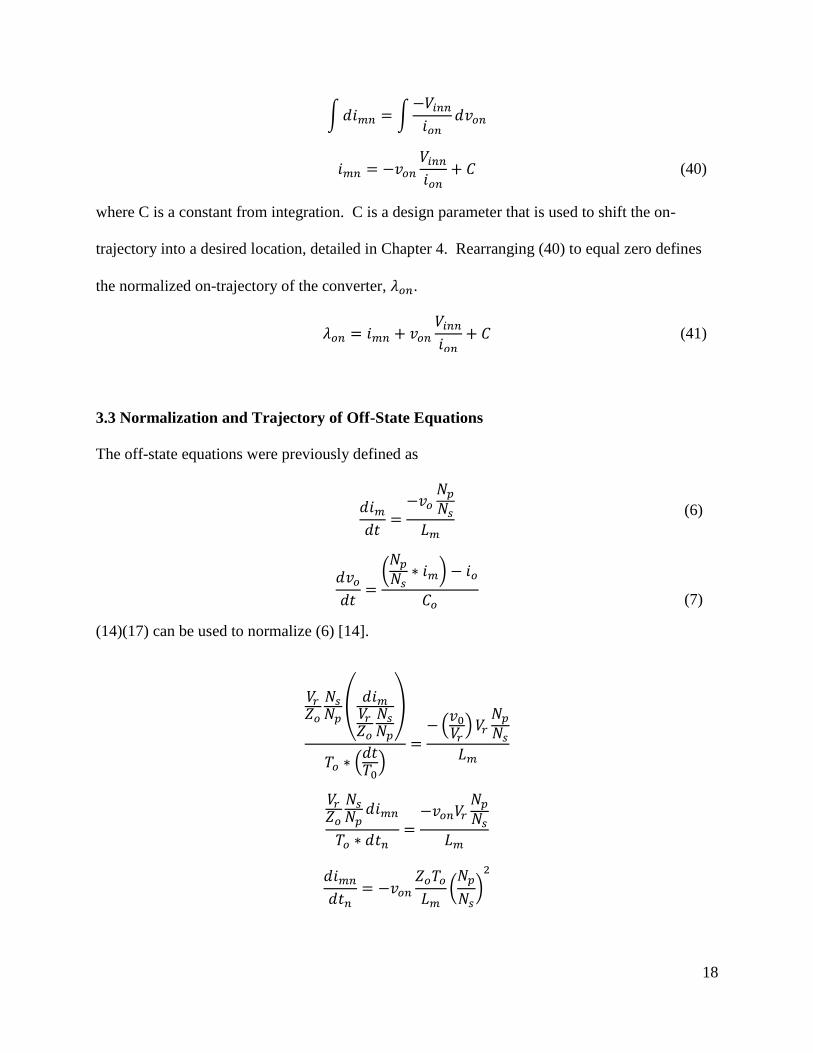
3.3 Normalization and Trajectory of Off-State Equations
The off-state equations were previously defined as
𝑑𝑖𝑚
𝑑𝑡=
−𝑣𝑜
𝑁𝑝
𝑁𝑠
𝐿𝑚
(6)
𝑑𝑣𝑜
𝑑𝑡=
(𝑁𝑝
𝑁𝑠∗ 𝑖𝑚) − 𝑖𝑜
𝐶𝑜
(7)
(14)(17) can be used to normalize (6) [14].
𝑉𝑟
𝑍𝑜
𝑁𝑠
𝑁𝑝(
𝑑𝑖𝑚𝑉𝑟
𝑍𝑜
𝑁𝑠
𝑁𝑝
)
𝑇𝑜 ∗ (𝑑𝑡𝑇0
)=
− (𝑣0
𝑉𝑟) 𝑉𝑟
𝑁𝑝
𝑁𝑠
𝐿𝑚
𝑉𝑟
𝑍𝑜
𝑁𝑠
𝑁𝑝𝑑𝑖𝑚𝑛
𝑇𝑜 ∗ 𝑑𝑡𝑛=
−𝑣𝑜𝑛𝑉𝑟
𝑁𝑝
𝑁𝑠
𝐿𝑚
𝑑𝑖𝑚𝑛
𝑑𝑡𝑛= −𝑣𝑜𝑛
𝑍𝑜𝑇𝑜
𝐿𝑚(
𝑁𝑝
𝑁𝑠)
2

19
𝑑𝑖𝑚𝑛
𝑑𝑡𝑛= −𝑣𝑜𝑛
𝑁𝑠
𝑁𝑝√
𝐿𝑚
𝐶02𝜋
𝑁𝑠
𝑁𝑝√𝐿𝑚𝐶𝑜
𝐿𝑚(
𝑁𝑝
𝑁𝑠)
2
𝑑𝑖𝑚𝑛
𝑑𝑡𝑛= −𝑣𝑜𝑛2𝜋 (42)
Continuing with normalizing (7)
𝑉𝑟 (𝑑𝑣𝑜
𝑉𝑟)
𝑇𝑜 (𝑑𝑡𝑇𝑜
)=
(𝑖𝑚
𝑉𝑟
𝑍𝑜
𝑁𝑠
𝑁𝑝
)𝑉𝑟
𝑍𝑜
𝑁𝑠
𝑁𝑝
𝑁𝑝
𝑁𝑠
𝐶𝑜−
( 𝑖𝑜 𝑉𝑟𝑍𝑜
)𝑉𝑟
𝑍𝑜
𝐶𝑜
𝑉𝑟𝑑𝑣𝑜𝑛
𝑇𝑜𝑑𝑡𝑛=
𝑖𝑚𝑛𝑉𝑟
𝑍𝑜
𝐶𝑜−
𝑖𝑜𝑛𝑉𝑟
𝑍𝑜
𝐶𝑜
𝑑𝑣𝑜𝑛
𝑑𝑡𝑛=
𝑇0
𝐶𝑜𝑍𝑜
(𝑖𝑚𝑛 − 𝑖𝑜𝑛)
𝑑𝑣𝑜𝑛
𝑑𝑡𝑛=
2𝜋𝑁𝑠
𝑁𝑝√𝐿𝑚𝐶𝑜
𝐶𝑜𝑁𝑠
𝑁𝑝√
𝐿𝑚
𝐶0
(𝑖𝑚𝑛 − 𝑖𝑜𝑛)
𝑑𝑣𝑜𝑛
𝑑𝑡𝑛= 2𝜋(𝑖𝑚𝑛 − 𝑖𝑜𝑛) (43)
To solve for the complete trajectory during the off state, (42) and (43) must be solved together.
Taking the derivative of (42) and substituting into (43) results in
𝑑2𝑖𝑚𝑛
𝑑𝑡𝑛2
= −2𝜋𝑑𝑣𝑜𝑛
𝑑𝑡𝑛
𝑑𝑣𝑜𝑛
𝑑𝑡𝑛=
−1
2𝜋 𝑑2𝑖𝑚𝑛
𝑑𝑡𝑛2
(44)
2𝜋(𝑖𝑚𝑛 − 𝑖𝑜𝑛) =−1
2𝜋 𝑑2𝑖𝑚𝑛
𝑑𝑡𝑛2
2𝜋𝑖𝑚𝑛 +1
2𝜋 𝑑2𝑖𝑚𝑛
𝑑𝑡𝑛2
− 2𝜋𝑖𝑜𝑛 = 0 (45)

20
Laplace transform can be used to solve (45) [14].
2𝜋 𝐼𝑚𝑛(𝑠) +1
2𝜋(𝑠2𝐼𝑚𝑛(𝑠) − 𝑠𝑖𝑚𝑛(0) −
𝑑𝑖𝑚𝑛(0)
𝑑𝑡𝑛) − 2𝜋
𝑖𝑜𝑛
𝑠= 0
𝐼𝑚𝑛(𝑠)(𝑠2 + (2𝜋)2) = 𝑠𝑖𝑚𝑛(0) +𝑑𝑖𝑚𝑛(0)
𝑑𝑡𝑛+ (2𝜋)2
𝑖𝑜𝑛
𝑠
𝐼𝑚𝑛(𝑠) = 𝑖𝑚𝑛(0)𝑠
(𝑠2 + (2𝜋)2)+
𝑑𝑖𝑚𝑛(0)
𝑑𝑡𝑛
1
(𝑠2 + (2𝜋)2)+ 𝑖𝑜𝑛
(2𝜋)2
𝑠(𝑠2 + (2𝜋)2) (46)
All of the add-ins are in a standard inverse Laplace format except the last add-in of (46). Using
the method of partial fractions
𝑖𝑜𝑛
(2𝜋)2
𝑠(𝑠2 + (2𝜋)2)= 𝑖𝑜𝑛
1
𝑠− 𝑖𝑜𝑛
𝑠
(𝑠2 + (2𝜋)2) (47)
Substituting (47) into (46) and inverse Laplace transforming, the result is
𝑖𝑚𝑛(𝑡𝑛) = 𝑖𝑚𝑛(0) cos(2𝜋𝑡𝑛) +
𝑑𝑖𝑚𝑛(0)𝑑𝑡𝑛
2𝜋sin(2𝜋𝑡𝑛) + 𝑖𝑜𝑛 − 𝑖𝑜𝑛 cos(2𝜋𝑡𝑛)
𝑖𝑚𝑛(𝑡𝑛) = 𝑖𝑜𝑛 + cos(2𝜋𝑡𝑛) (𝑖𝑚𝑛(0) − 𝑖𝑜𝑛) +𝑑𝑖𝑚𝑛(0)
𝑑𝑡𝑛
1
2𝜋sin(2𝜋𝑡𝑛) (48)
(48) can be seen to be dependent upon 𝑡𝑛 which is not conductive for a normalization of the
converter. Therefore, the next steps are performed with the goal of removing the dependence of
𝑡𝑛. Using the trigonometric identity 𝑎 ∗ sin(𝑥) + 𝑏 ∗ cos(𝑥) = √𝑎2 + 𝑏2 ∗ sin (𝑥 + tan−1 (𝑏
𝑎))
to (48) [16]
𝑖𝑚𝑛(𝑡𝑛) = 𝑖𝑜𝑛 + √𝑎2 + 𝑏2 ∗ sin (2𝜋𝑡𝑛 + tan−1 (𝑏
𝑎)) (49)
where
𝑎 =𝑑𝑖𝑚𝑛(0)
𝑑𝑡𝑛
1
2𝜋 (50)
𝑏 = (𝑖𝑚𝑛(0) − 𝑖𝑜𝑛) (51)
taking the derivative of (49) and equating to (42) results in

21
−𝑣𝑜𝑛2𝜋 = 2𝜋√𝑎2 + 𝑏2 ∗ cos (2𝜋𝑡𝑛 + tan−1 (𝑏
𝑎)) (52)
To remove the tragicomic function dependent upon 𝑡𝑛 in (52), the tragicomic identity
cos (sin−1(𝑥)) = √1 − 𝑥2 can be applied [17] [14]. Solving (49) for the arcsin
sin (2𝜋𝑡𝑛 + tan−1 (𝑏
𝑎)) =
𝑖𝑚𝑛 − 𝑖𝑜𝑛
√𝑎2 + 𝑏2
2𝜋𝑡𝑛 + tan−1 (
𝑏
𝑎) = sin−1 (
𝑖𝑚𝑛 − 𝑖𝑜𝑛
√𝑎2 + 𝑏2)
(53)
(53) can now be substituted into the inside of the tragicomic function in (52) and simplified with
the tragicomic identity discussed above
−𝑣𝑜𝑛2𝜋 = 2𝜋√𝑎2 + 𝑏2 ∗ cos (sin−1 (𝑖𝑚𝑛 − 𝑖𝑜𝑛
√𝑎2 + 𝑏2))
−𝑣𝑜𝑛2𝜋 = 2𝜋√𝑎2 + 𝑏2√1 − (
𝑖𝑚𝑛 − 𝑖𝑜𝑛
√𝑎2 + 𝑏2)
2
𝑣𝑜𝑛2 = (𝑎2 + 𝑏2) (1 − (
𝑖𝑚𝑛 − 𝑖𝑜𝑛
√𝑎2 + 𝑏2)
2
)
𝑣𝑜𝑛2 = (𝑎2 + 𝑏2) + (𝑖𝑚𝑛 − 𝑖𝑜𝑛)2
(𝑎2 + 𝑏2) = 𝑣𝑜𝑛2 + (𝑖𝑚𝑛 − 𝑖𝑜𝑛)2 (54)
where a and b are still
𝑎 =𝑑𝑖𝑚𝑛(0)
𝑑𝑡𝑛
1
2𝜋 (50)
𝑏 = (𝑖𝑚𝑛(0) − 𝑖𝑜𝑛) (51)
Observing (54), the equation is in the format of a circle. In the 𝑣𝑜𝑛 vs. 𝑖𝑚𝑛 plane, the center of
the circle would be (0, 𝑖𝑜𝑛) and the radius, r, would be
𝑟 = √𝑎2 + 𝑏2 (55)

22
𝑟 = √(𝑑𝑖𝑚𝑛(0)
𝑑𝑡𝑛
1
2𝜋)
2
+ (𝑖𝑚𝑛 − 𝑖𝑜𝑛)2 (56)
which is completely dependent upon the operating conditions of the converter. Rearranging (54)
to equal zero, the normalize off-state trajectory can be defined as
𝜆𝑜𝑓𝑓 = 𝑣𝑜𝑛2 + (𝑖𝑚𝑛 − 𝑖𝑜𝑛)2 − (𝑎2 + 𝑏2) (57)
3.4 Summary of the Normalizing Equations and Normalized Trajectories
This subsection serves to summarize the three previous subsections in this chapter for the
normalizing equations and the normalized trajectories [14]. The converter specific normalizing
equations are
𝑉𝑖𝑛𝑛 =
𝑉𝑖𝑛
𝑉𝑟
𝑁𝑝
𝑁𝑠
(14)
𝑖𝑚𝑛 =
𝑖𝑚
𝑉𝑟
𝑍𝑜
𝑁𝑠
𝑁𝑝
(15)
𝑣𝑜𝑛 =𝑣𝑜
𝑉𝑟 (16)
𝑖𝑜𝑛 =
𝑖𝑜
𝑉𝑟
𝑍𝑜
(17)
where 𝑣𝑥, 𝑖𝑥, and t are the variables that are to be normalized and
𝑍𝑜 =𝑁𝑠
𝑁𝑝√
𝐿𝑚
𝐶0 (34)
𝑇𝑜 = 2𝜋𝑁𝑠
𝑁𝑝√𝐿𝑚𝐶𝑜 (36)
The on-state normalized trajectory was derived as
𝜆𝑜𝑛 = 𝑖𝑚𝑛 + 𝑣𝑜𝑛
𝑉𝑖𝑛𝑛
𝑖𝑜𝑛+ 𝐶 (41)

23
where C is a design parameter selected to place the converter in the desired operating condition.
(41) is observed to be a downward sloping line in the 𝑣𝑜𝑛 vs. 𝑖𝑚𝑛 plane. Finally, the off-state
trajectory was derived as
(𝑎2 + 𝑏2) = 𝑣𝑜𝑛2 + (𝑖𝑚𝑛 − 𝑖𝑜𝑛)2 (54)
where
𝑎 =𝑑𝑖𝑚𝑛(0)
𝑑𝑡𝑛
1
2𝜋 (50)
𝑏 = (𝑖𝑚𝑛(0) − 𝑖𝑜𝑛) (51)
which in the 𝑣𝑜𝑛 vs. 𝑖𝑚𝑛 plane is a circle with the center located at (0, 𝑖𝑜𝑛) and the radius, r,
equal to
𝑟 = √(𝑑𝑖𝑚𝑛(0)
𝑑𝑡𝑛
1
2𝜋)
2
+ (𝑖𝑚𝑛 − 𝑖𝑜𝑛)2 (56)
r is completely dependent upon the operating conditions of the converter. Rearranged to equal
zero, the off-state trajectory can be defined as
𝜆𝑜𝑓𝑓 = 𝑣𝑜𝑛2 + (𝑖𝑚𝑛 − 𝑖𝑜𝑛)2 − (𝑎2 + 𝑏2) (57)

24
IV. Proposed Control Law and Simulations
4.1 Graphical Analysis of the NSS Trajectories
Figure 8 shows a graph of the NSS trajectories derived in Chapter 3 and summarized in Section
3.4. This graph is for a generic flyback converter, with arbitrary trajectory placement in the
𝑣𝑜𝑛 vs. 𝑖𝑚𝑛 plane. As previously described, the on-state trajectory is a downward sloping line
and the off-state trajectory is a circle, generically pictured here with a center at (0,0). This
section attempts to explain how the two trajectories interact with each other and how they relate
to the operation of the converter.
Looking at the 𝑣𝑜𝑛 vs. 𝑖𝑚𝑛 plane and thinking of the flyback converter as a whole, immediately
quadrants of the plane can be identified as unobtainable or undesirable areas of operation based
off the variable’s polarity [14]. 𝑖𝑚𝑛 can only be positive for the flyback converter to be
operating properly. Therefore, 𝑖𝑚𝑛 would not be obtainable in quadrants III or IV. 𝑣𝑜𝑛 would
not be desired to be negative either. This would imply that the load was transferring power to
Figure 8: Generic NSS Graph

25
the input of the converter. Therefore, 𝑣𝑜𝑛 should not operate in quadrants II or III. That leaves
only quadrant I as the operational quadrant which satisfies both variables’ conditions. In
quadrant I, 𝑖𝑚𝑛 and 𝑣𝑜𝑛 are both positive and the flyback converter would be transferring power
to the load. The undesired quadrants have been grayed out in Figure 8.
Movement along the trajectories during steady-state can be determined by considering the
flyback operation in each state [14]. As discussed in II. Flyback Converter Operation, during the
on-state 𝑖𝑚 is increasing, storing energy in the transformer’s magnetic field from 𝑉𝑖𝑛, and 𝑣𝑜 is
decreasing, due to the load using up the energy stored in the output capacitor. Therefore, the
converter operation would force the converter to slide up the trajectory during the on-state, as
shown in Figure 9(a). During the off-state, 𝑖𝑚 is decreasing, supplying the transformer’s stored
energy to the load and output capacitor, while 𝑣𝑜 is increasing, due to the transformer’s supplied
energy. Therefore, operation would force the converter to slide down the trajectory during the
off-state, as shown in Figure 9(b).
(a) (b)
Figure 9: NSS Trajectory Sliding Direction: (a) on-state, (b) off-state
26
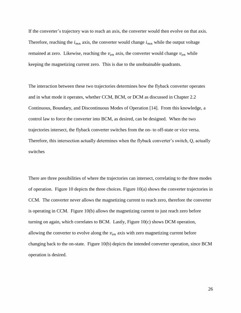
If the converter’s trajectory was to reach an axis, the converter would then evolve on that axis.
Therefore, reaching the 𝑖𝑚𝑛 axis, the converter would change 𝑖𝑚𝑛 while the output voltage
remained at zero. Likewise, reaching the 𝑣𝑜𝑛 axis, the converter would change 𝑣𝑜𝑛 while
keeping the magnetizing current zero. This is due to the unobtainable quadrants.
The interaction between these two trajectories determines how the flyback converter operates
and in what mode it operates, whether CCM, BCM, or DCM as discussed in Chapter 2.2
Continuous, Boundary, and Discontinuous Modes of Operation [14]. From this knowledge, a
control law to force the converter into BCM, as desired, can be designed. When the two
trajectories intersect, the flyback converter switches from the on- to off-state or vice versa.
Therefore, this intersection actually determines when the flyback converter’s switch, Q, actually
switches
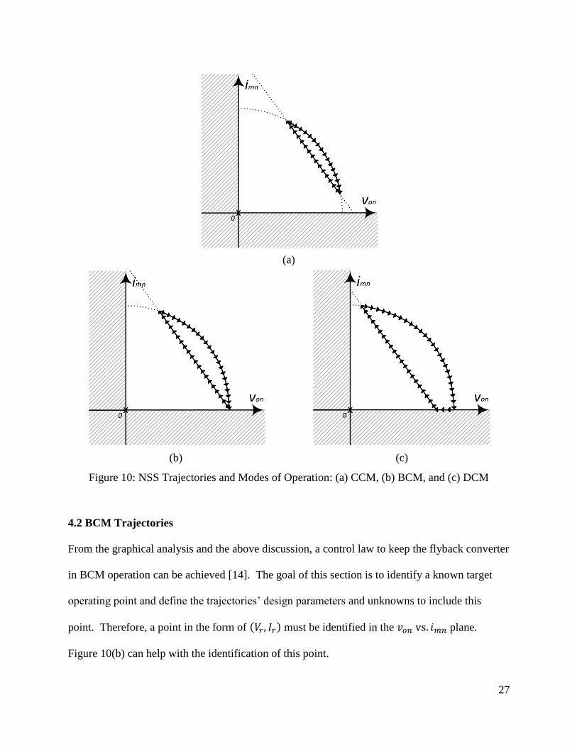
There are three possibilities of where the trajectories can intersect, correlating to the three modes
of operation. Figure 10 depicts the three choices. Figure 10(a) shows the converter trajectories in
CCM. The converter never allows the magnetizing current to reach zero, therefore the converter
is operating in CCM. Figure 10(b) allows the magnetizing current to just reach zero before
turning on again, which correlates to BCM. Lastly, Figure 10(c) shows DCM operation,
allowing the converter to evolve along the 𝑣𝑜𝑛 axis with zero magnetizing current before
changing back to the on-state. Figure 10(b) depicts the intended converter operation, since BCM
operation is desired.
27
(a)
(b) (c)
Figure 10: NSS Trajectories and Modes of Operation: (a) CCM, (b) BCM, and (c) DCM
4.2 BCM Trajectories
From the graphical analysis and the above discussion, a control law to keep the flyback converter
in BCM operation can be achieved [14]. The goal of this section is to identify a known target
operating point and define the trajectories’ design parameters and unknowns to include this
point. Therefore, a point in the form of (𝑉𝑟, 𝐼𝑟) must be identified in the 𝑣𝑜𝑛 vs. 𝑖𝑚𝑛 plane.
Figure 10(b) can help with the identification of this point.

28
From Figure 10(b), we can identify a known point at the intersection of the on- and off-state
trajectory on the von axis. Setting the reference voltage to the desired output voltage
𝑉𝑟 = 𝑉𝑜 (58)
𝑣𝑜𝑛 =𝑣𝑜
𝑉𝑟 (16)
𝑣𝑜𝑛 =𝑣𝑜
𝑉𝑜= 1 (59)
As previously discussed, BCM is achieved by switching from the off- to on-state just as the
magnetizing current reaches zero. Therefore, the desired current at turn-on is
𝑖𝑚𝑛 = 0
A trajectory point is now known as
(𝑉𝑟 , 𝐼𝑟) = (1,0) (60)
Using this known trajectory point, we can solve for the constant C in the on-state trajectory and
the initial conditions of the off-state trajectory. Plugging in (60) into (42), C can be solved for.
0 = 0 + 1𝑉𝑖𝑛𝑛
𝑖𝑜𝑛+ 𝐶
𝐶 = −𝑉𝑖𝑛𝑛
𝑖𝑜𝑛 (61)
Therefore, the complete BCM on-state trajectory is
𝜆𝑜𝑛 = 𝑖𝑚𝑛 + 𝑣𝑜𝑛
𝑉𝑖𝑛𝑛
𝑖𝑜𝑛−
𝑉𝑖𝑛𝑛
𝑖𝑜𝑛 (62)
Moving on to the off-state trajectory, a and b can be simplified with the known trajectory point.
Knowing 𝑣𝑜𝑛 = 1, (42) can be simplified to
𝑑𝑖𝑚𝑛(0)
𝑑𝑡𝑛= −2𝜋 (63)
Substituting (63) into (50), the equation for a can be reduced to
𝑎 = −1 (64)

29
(51), the equation for b, can now also be simplified down to
𝑏 = −𝑖𝑜𝑛 (65)
Substituting (64) and (65) into (57), the complete BCM off-state trajectory is defined as
𝜆𝑜𝑓𝑓 = 𝑣𝑜𝑛2 + (𝑖𝑚𝑛 − 𝑖𝑜𝑛)2 − 1 − 𝑖𝑜𝑛
2 (66)
(62) and (66) defined the on- and off-state trajectories for BCM operation [14].
4.3 Steady-State BCM Control Law
The goal of a control law is to force the converter to move to or stay on the identified BCM
trajectories. Knowing the movements along the trajectories for each state of Q and the above
conditions, a control law can be developed. The control law decides between two options: either
Q should be on or Q should be off. The decision is based off the current state of Q and the
relative location of the current operating point to the BCM trajectories.
Figure 11(a) depicts the control law and possible converter trajectories for when Q is on. As
previously discussed, while Q is on, the converter will move up the plane. If the converter is
currently operating below the off-trajectory, Q is kept on while the converter continues to move
up the plane until the off-state trajectory is reached. Once the off-state trajectory is reached, Q is
switched off. If the converter is operating anywhere above the off-trajectory, then Q should be
turned off [14].
Figure 11(b) shows the control law and possible converter trajectories for when Q is off.
Remembering the desired to operate in BCM, the first part of the law is that Q is not allowed to

30
(a) (b)
Figure 11: BCM Control Law Trajectories when: (a) Q is ON, (b) Q is OFF [14]
switch back on until imn = 0, once it has been switched off. Therefore, if the converter is
operating anywhere above the von axis (imn > 0), Q is kept off until the converter reaches the von
axis. Once the von axis is reached, the current operating point is compared to the off-state
trajectory. If the converter is operating greater than the off-state trajectory, Q is kept off,
allowing the converter to evolve down the von axis to the off-state trajectory. If the converter is
operating below or at the off-state trajectory, Q is switched on, allowing the converter to ride the
on-state trajectory back up to the off-state trajectory as previously described [14].
Figure 12: BCM Control Law Flow Diagram

31
Figure 12 shows a complete flow diagram for the developed BCM control law. The above
control law forces the converter to move to and operate on the BCM trajectories, no matter
where the converter is currently operating, in one switching cycle. This allows the flyback
converter to operate in BCM continuously for any loading condition during steady-state. In a
transient situation, where the input voltage or load changes, the worst case scenario would be
that the converter recovers in one switching cycle. During that one transient switching cycle, a
DCM of operation with a slight over voltage output or a BCM of operation with a slight under
voltage output could be experienced. This is because the desired on- and off-state trajectories
change with converter parameter changes. Taking only one switching cycle to recover provides
remarkable stability and transient response time for all converter conditions.
Another significant benefit of keeping Q off, once switching off, until imn = 0 is that the effect of
chattering is eliminated. Chattering is defined as a condition where Q is repeatedly turned on
and off in quick succession to keep the actual converter trajectory infinitely close to the desired
trajectory. Figure 13 shows a hypothetical chattering situation. This would be avoided with the
proposed control law because only two definite switching locations are identified: at the
intersection of the on- and off-state trajectory and on the von axis.
Figure 13: Hypothetical Chattering Situation
Ideal trajectory - Dotted Line, Actual Trajectory - Solid Line

32
4.4 Steady-State Switching Frequency Derivation
The switching frequency of a converter is very important in considerations for EMI and
component selection including microcontroller or processor, semiconductor devices, current
sensors, and analog-to-digital (ADC) converters. This section will derive an accurate
approximation for the steady-state switching frequency using the proposed control laws. The
switching frequency is found to be dependent upon the average input and output voltage, turns
ratio of the transformer, and the transformer’s magnetizing inductance.
The normalized switching period, Tn, can be described as
𝑇𝑛 = 𝑡𝑜𝑛𝑛+ 𝑡𝑜𝑓𝑓𝑛
(67)
where 𝑡𝑜𝑛𝑛 and 𝑡𝑜𝑓𝑓𝑛
are the normalized values for the on and off time, respectively. 𝑡𝑜𝑛𝑛 and
𝑡𝑜𝑓𝑓𝑛 can be found by looking at the differential equations for 𝑖𝑚𝑛 in each state. For the on-state
𝑑𝑖𝑚𝑛
𝑑𝑡𝑛= 𝑉𝑖𝑛𝑛2𝜋 (37)
𝑡𝑜𝑛𝑛=
∆𝑖𝑚𝑛
𝑉𝑖𝑛𝑛2𝜋 (68)
and for the off-state
𝑑𝑖𝑚𝑛
𝑑𝑡𝑛= −𝑣𝑜𝑛2𝜋 (42)
𝑡𝑜𝑓𝑓𝑛=
∆𝑖𝑚𝑛
𝑉𝑜𝑛2𝜋 (69)
where 𝑑𝑡𝑛 is replaced with the state’s time length and 𝑑𝑖𝑚𝑛 is replaced with ∆𝑖𝑚𝑛. Note that
∆𝑖𝑚𝑛 is equal for both on- and off-states. Substituting (68) and (69) into (67)
𝑇𝑛 =∆𝑖𝑚𝑛
𝑉𝑖𝑛𝑛2𝜋+
∆𝑖𝑚𝑛
𝑉𝑜𝑛2𝜋
𝑇𝑛 =∆𝑖𝑚𝑛
2𝜋(
1
𝑉𝑜𝑛+
1
𝑉𝑖𝑛𝑛) (70)

33
Knowing that 𝑉𝑜𝑛 is equal to approximately 1 on average, (70) can be simplified down to
𝑇𝑛 =∆𝑖𝑚𝑛
2𝜋(1 +
1
𝑉𝑖𝑛𝑛) (71)
To convert the normalized period into the converter specific period, (12) can be used.
𝑇 =∆𝑖𝑚𝑛
2𝜋(1 +
1
𝑉𝑖𝑛𝑛) 𝑇𝑜 (72)
And therefore the switching frequency is
𝑓𝑠𝑤 =
2𝜋
∆𝑖𝑚𝑛𝑇𝑜 (1 +1
𝑉𝑖𝑛𝑛)
(73)
This equation is only helpful if you know ∆𝑖𝑚𝑛. Therefore, this will be the next step. As
previously discussed, and as will be seen in more detail in the simulations to follow, in steady-
state operation, ∆𝑖𝑚𝑛’s extremes are at the intersection of the on- and off-state trajectory. One
extreme is where 𝑖𝑚𝑛 = 0, which corresponds to 𝑉𝑜𝑛 = 1. The other intersection defines ∆𝑖𝑚𝑛
and here it is found that 𝑉𝑜𝑛 is close, but not equal to 1. To find this intersection and therefore
∆𝑖𝑚𝑛, the on- an off-state trajectories will be solved for 𝑉𝑜𝑛 then set equal to each other to
eliminate 𝑉𝑜𝑛. Following that, ∆𝑖𝑚𝑛 can then be solved for. Starting with the on- and off-state
trajectories, setting them equal to 0 since that is the objective of the control law, and substituting
𝑖𝑚𝑛 as ∆𝑖𝑚𝑛,
0 = 𝑣𝑜𝑛2 + (∆𝑖𝑚𝑛 − 𝑖𝑜𝑛)2 − 1 − 𝑖𝑜𝑛
2 (66)
𝑣𝑜𝑛 = √1 + 𝑖𝑜𝑛2 − (∆𝑖𝑚𝑛 − 𝑖𝑜𝑛)2
𝑣𝑜𝑛 = √1 − ∆𝑖𝑚𝑛2 + ∆𝑖𝑚𝑛2𝑖𝑜𝑛 (74)
0 = ∆𝑖𝑚𝑛 + 𝑣𝑜𝑛
𝑉𝑖𝑛𝑛
𝑖𝑜𝑛−
𝑉𝑖𝑛𝑛
𝑖𝑜𝑛 (62)
𝑣𝑜𝑛 = 1 − ∆𝑖𝑚𝑛
𝑖𝑜𝑛
𝑉𝑖𝑛𝑛 (75)

34
Equating together (74) and (75) and solving for ∆𝑖𝑚𝑛
1 − ∆𝑖𝑚𝑛
𝑖𝑜𝑛
𝑉𝑖𝑛𝑛= √1 − ∆𝑖𝑚𝑛
2 + ∆𝑖𝑚𝑛2𝑖𝑜𝑛
∆𝑖𝑚𝑛 =2𝑖𝑜𝑛 (1 +
1𝑉𝑖𝑛𝑛
)
1 + (𝑖𝑜𝑛
𝑉𝑖𝑛𝑛)
2 (76)
It can be observed that the denominator is nearly 1, therefore it can be neglected.
∆𝑖𝑚𝑛 = 2𝑖𝑜𝑛 (1 +1
𝑉𝑖𝑛𝑛) (77)
Substituting (77) into (73) and (36) for 𝑇𝑜, the switching frequency dependent upon normalized
values is
𝑓𝑠𝑤 =
𝑁𝑝/𝑁𝑠
2𝑖𝑜𝑛√𝐿𝑚𝐶𝑜 (1 +1
𝑉𝑖𝑛𝑛)
2 (78)
Using equations (14), (17), (34), and substituting 𝑉𝑟 and 𝑉𝑜, the switching frequency can be
described in non-normalized converter values as
𝑓𝑠𝑤 =𝑉𝑜 ∗ 𝑁𝑝/𝑁𝑠
2 𝑖𝑜𝑍𝑜√𝐿𝑚𝐶𝑜 (1 +𝑉𝑟
𝑁𝑝
𝑁𝑠
𝑉𝑖𝑛)
2
𝑓𝑠𝑤 =𝑉𝑜 ∗ (
𝑁𝑝
𝑁𝑠)
2
2𝑖𝑜𝐿𝑚 (1 +𝑉𝑟𝑁𝑝
𝑉𝑖𝑛𝑁𝑠)
2 (79)
4.5 Simulations of Steady-State BCM Control Law
The control law proposed above was implemented in MATLAB/Simulink©
. Figure 14-16Error!
Reference source not found. shows the Simulink©
implementation of the flyback converter and
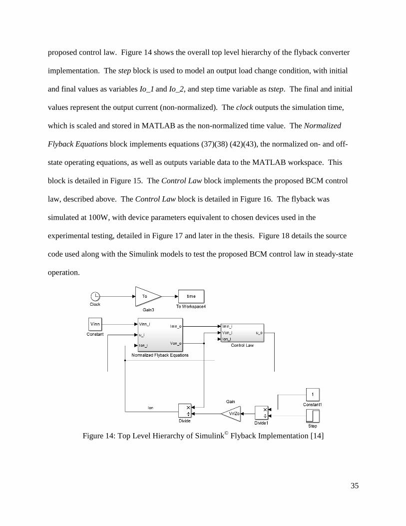
35
proposed control law. Figure 14 shows the overall top level hierarchy of the flyback converter
implementation. The step block is used to model an output load change condition, with initial
and final values as variables Io_1 and Io_2, and step time variable as tstep. The final and initial
values represent the output current (non-normalized). The clock outputs the simulation time,
which is scaled and stored in MATLAB as the non-normalized time value. The Normalized
Flyback Equations block implements equations (37)(38) (42)(43), the normalized on- and off-
state operating equations, as well as outputs variable data to the MATLAB workspace. This
block is detailed in Figure 15. The Control Law block implements the proposed BCM control
law, described above. The Control Law block is detailed in Figure 16. The flyback was
simulated at 100W, with device parameters equivalent to chosen devices used in the
experimental testing, detailed in Figure 17 and later in the thesis. Figure 18 details the source
code used along with the Simulink models to test the proposed BCM control law in steady-state
operation.
Figure 14: Top Level Hierarchy of Simulink
© Flyback Implementation [14]

36
Figure 15: Normalized Flyback Equations Simulink
© Block [14]
37
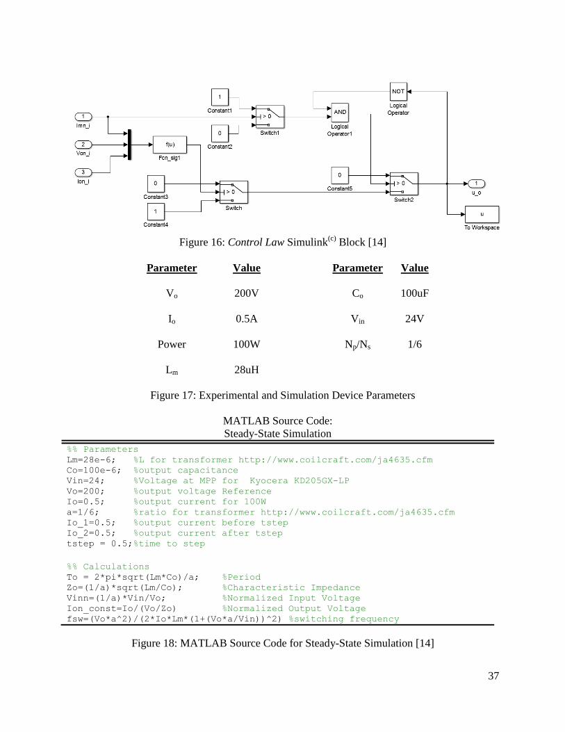
Figure 16: Control Law Simulink
(c) Block [14]
Parameter Value Parameter Value
Vo 200V Co 100uF
Io 0.5A Vin 24V
Power 100W Np/Ns 1/6
Lm 28uH
Figure 17: Experimental and Simulation Device Parameters
MATLAB Source Code:
Steady-State Simulation
%% Parameters Lm=28e-6; %L for transformer http://www.coilcraft.com/ja4635.cfm Co=100e-6; %output capacitance Vin=24; %Voltage at MPP for Kyocera KD205GX-LP Vo=200; %output voltage Reference Io=0.5; %output current for 100W a=1/6; %ratio for transformer http://www.coilcraft.com/ja4635.cfm Io_1=0.5; %output current before tstep Io_2=0.5; %output current after tstep tstep = 0.5;%time to step
%% Calculations To = 2*pi*sqrt(Lm*Co)/a; %Period Zo=(1/a)*sqrt(Lm/Co); %Characteristic Impedance Vinn=(1/a)*Vin/Vo; %Normalized Input Voltage Ion_const=Io/(Vo/Zo) %Normalized Output Voltage fsw=(Vo*a^2)/(2*Io*Lm*(1+(Vo*a/Vin))^2) %switching frequency
Figure 18: MATLAB Source Code for Steady-State Simulation [14]

38
Figure 19 shows the simulation results for the on- and off-state trajectories of the steady-state
BCM control law implementation for one switching cycle. From this figure, it is notable that the
on-state trajectory is a straight line and the off-state trajectory is an arc of a circle (the circle is
distorted in the figure due to axis scaling). The converter changes from the off-state to the on-
state once the converter reaches imn = 0, meaning the converter is operating in BCM as desired.
Figure 20 shows the steady-state primary and secondary current while Figure 21 shows the
steady-state output voltage. The primary and secondary current are clearly operating in BCM;
once the secondary current reaches zero, the primary current instantly starts increasing. The
output voltage has a ripple less than 0.09V (also shown by Figure 19), which corresponds to less
than 0.05%. The average value is equal to 199.97V, which is only a 0.015% error from the
desired 200V reference. From equation (79), the switching frequency is approximated to be
34.77kHz for these operating conditions. The switching frequency is measured to be 34.81kHz
from the simulations, which is an error of 0.12%.
Figure 19: Simulink
© Steady-State Simulation of Trajectories

39
Figure 20: Simulink©
Steady-State Simulation: Ip and Is
Figure 21: Simulink
© Steady-State Simulation: Vo
4.6 Transient Response of BCM Control Law
A transient response happens when the input voltage or loading condition changes. The transient
lasts for only one switching cycle, assuming the change is completed in one switching cycle, due

40
to the proposed control law forcing the converter to the NSS. This allows for an extremely fast
transient response. Depending on when the voltage or load changes constitutes how the
converter will react. The only two options for the converter operation with the proposed control
law is to continue in BCM or operate in DCM for one switching cycle.
If the off-trajectory radius is decreased (by a change in output current or input voltage) while the
converter is operating past the new radius value, the converter will operate in DCM for one
switching cycle. This is due to the fact that to get back to a lower radius trajectory, the converter
must evolve down the von axis. This will result in a slightly larger overshoot of the output
voltage compared to steady-state for one switching cycle. If the change occurs while the
converter is operating below the new off-trajectory radius, no transient will occur. Figure 22
shows an example of a DCM transient. The key point of this figure is the transient trajectory
which evolves down the von axis. This is not the only situation where a DCM operation could
occur, but just one example.
In comparison, if the off-trajectory radius is extended, the converter will still operate in BCM. If
the change is during the on-state, no transient will be experienced. If the change is during the
off-state however, the converter will undershoot the new trajectory. In the next switching cycle,
the converter will recover and operate back on the desired trajectories. This will result in a
slightly lower output voltage and higher peak input current compared to steady-state for one
switching cycle. Figure 23 shows an example of an undershooting BCM transient. The
undershooting transient is observable with the larger peak current.

41
Figure 22: Transient Trajectory: DCM
Figure 23: Transient Trajectory: BCM
Analyzing the undershooting BCM transient, a modification of the control law could be
potentially be proposed. During the off trajectory, if Q was turned on the instant the off-

42
trajectory crossed the on-trajectory, the undershooting voltage and increase peak current would
be avoided. This would force the converter to operate in CCM, never reaching 0A during the
transient. While this is a viable solution to improve the transient, the modification was omitted
due to creating potential chattering issues during steady-state and increasing control complexity.
Another note about Figure 22 and Figure 23 is that during steady-state, both loading conditions
operated in BCM automatically. This was intended and one of the main points of the proposed
control method.
4.7 Start-Up Operation and Max Input Current Protection
Now that the control law’s steady-state and transient characteristics have been analyzed, one last
unique situation is converter start-up. Using the proposed BCM control law during start up, the
flyback converter would experience an extreme input and magnetizing current peak. This is due
to the control law bringing the output voltage to the reference value in one switching cycle; this
would obviously requires a large amount of energy since the converter is starting with 0V output.
The start-up trajectory is shown in Figure 24. Here, the peak input current reaches 375A, which
is obviously unacceptable for common devices. The settling time (defined here as the time for
the output voltage to be bounded within 5% of its desired value) is only 0.841ms, shown in the
output voltage waveform in Figure 25.

43
Figure 24: Start-Up Trajectory
Figure 25: Start-Up Output Voltage
To fix the large start-up input current, a maximum input current level can be set. This is a
desirable addition to the control law because it protects the input devices (such as the

44
semiconductor switch and transformer) from exceeding the current ratings and damaging the
devices. Therefore, a peak input current value can be selected based off the device ratings. This
value could then be normalized based off (15) if desired.
For this specific controller design, the peak input current was set to a non-normalized value of
20A. Figure 26 shows the updated control law flow diagram with the peak limitation addition.
Figure 27 details the updated Simulink©
control law block. Figure 28 shows the start-up
trajectory with the current maximum implemented. As expected, the current never exceeds 20A.
The converter now takes multiple switching cycles to reach the desired voltage reference. As
described before, the load of the converter is modeled as purely resistive; therefore, the output
current is actually a function of the output voltage. In the start-up situation, the output current is
increasing with the output voltage until the desired voltage reference is reached. Here, the
controller is still operating in BCM during the start-up, forcing the magnetizing current to zero
before turning Q back on. Figure 29 shows the effects of limiting the input current. The
converter’s output voltage settling time drastically increased from 0.841ms to 30.1ms, which is
an undesirable effect.
Figure 26: BCM Control Law Flow Diagram with Input Current Limit, BCM Start-Up

45
Figure 27: Control Law Simulink© Block with Input Current Limit, BCM Start-Up
Figure 28: Start-Up Trajectory with Input Current Limit, BCM Start-Up

46
Figure 29: Start-Up Output Voltage with Input Current Limit, BCM Start-Up
To decrease the settling time, the start-up control was modified to operate in CCM, with a set
∆𝑖𝑚𝑛, instead of operating in BCM. This allowed for a larger amount of energy to transfer faster,
while still limiting the peak current. 𝑖𝑚𝑛 oscillated between the defined peak, 𝑖𝑚𝑛𝑝𝑘 and
𝑖𝑚𝑛𝑝𝑘− ∆𝑖𝑚𝑛. This control was chosen to be implemented any time the converter is operating
below the settling range (5% of Vr, which in this converter 190V). The transition location
between the CCM and BCM control method was selected arbitrarily and could be changed for
each application, depending on the expect peak current and settling times. The longer the CCM
control method operates during start up (the closer the transition is to steady-state operation), the
faster the settling time will be. A potential issue though is getting the transition too close to
steady-state and causing a chattering situation in the converter where the control law is switching

47
from BCM to CCM operation from a small transient. Therefore, the 5% of 𝑉𝑟 boundary was
selected.
For this converter design, ∆𝑖𝑚𝑛 = 5𝐴. Again, this was an arbitrary selection. The smaller
the ∆𝑖𝑚𝑛, the faster the settling time will be. The negative effects of a smaller ∆𝑖𝑚𝑛 is a higher
switching frequency, which could affect EMI, increase start-up losses, and cause higher average
power dissipation through the devices. 5A seemed to be an acceptable trade off in this
application based off the selected components and operating current.
Figure 30 shows the updated flow diagram for the CCM start-up method. Figure 31 shows the
updated Control Law block for the CCM start-up. Figure 32 and Figure 33 show the start-up
trajectory with the CCM start-up control. Figure 32 shows the first few switching cycles of start-
up. It is clear that the converter is now operating in CCM with a ∆𝑖𝑚𝑛 of 5A and peak of 20A.
Figure 33 highlights the transition from CCM to BCM at 190V (5% of 𝑉𝑟). From there, BCM
control continues to and during steady-state. The benefit of this modified control is shown in
Figure 34. The settling time decreased to 13.5ms, a 55.1% reduction compared to the BCM
start-up of Figure 29.

48
Figure 30:BCM Control Law Flow Diagram with Input Current Limit, CCM Start-Up
Figure 31: Control Law Simulink© Block with Input Current Limit, CCM Start-Up
49
Figure 32: Start-Up Trajectory with Input Current Limit, CCM Start-Up
Figure 33: Start-Up Trajectory with Input Current Limit, CCM to BCM Transition

50
Figure 34: Start-Up Output Voltage with Input Current Limit, CCM Start-Up
4.8 Review of Proposed Control
This section has presented the proposed control law for operating the flyback converter in BCM
control under any loading condition. The on-state trajectory was derived as
𝜆𝑜𝑛 = 𝑖𝑚𝑛 + 𝑣𝑜𝑛
𝑉𝑖𝑛𝑛
𝑖𝑜𝑛−
𝑉𝑖𝑛𝑛
𝑖𝑜𝑛 (62)
while the off-state trajectory was derived as
𝜆𝑜𝑓𝑓 = 𝑣𝑜𝑛2 + (𝑖𝑚𝑛 − 𝑖𝑜𝑛)2 − 1 − 𝑖𝑜𝑛
2 (66)
With the known trajectories, the switching frequency was derived as
𝑓𝑠𝑤 =𝑉𝑜 ∗ (
𝑁𝑝
𝑁𝑠)
2
2𝑖𝑜𝐿𝑚 (1 +𝑉𝑟𝑁𝑝
𝑉𝑖𝑛𝑁𝑠)
2 (80)
The proposed law allowed for swift response to transients in just one switching cycle. This
control was analyzed and modeled in Simulink©/MATLAB. In addition to steady-state and
transient response, start-up was also analyzed. It was determined that the best method for

51
managing start-up input current peaks and settling time was to operate with a maximum input
current limit as well as operating in CCM during start-up. Figure 30 shows the complete final
flow diagram for the proposed control.

52
V. Hardware Design and Component Selection
5.1 Overview and Hardware Design Considerations
While the flyback itself presents a minimal component converter topology, combining all the
required parts for control, power, and signal compensation can tally up quite quickly. This
chapter will step through each major section of the hardware implementation and selection for an
intended 100W flyback converter, implementing the NSS control detailed in Chapter 4.
Realistically, the tested flyback converter was only capable of 90W due to saturating the
transformer.
Implementation of the control law was performed in a Digital Signature Processor (DSP). The
necessary feedback signal variables to implement the NSS control included the output voltage,
primary current, secondary current, and output current. The input voltage was not required for
the designed NSS control, but is a variable in the NSS trajectories. Therefore, feedback network
to acquire the input voltage was include incase this signal was required in future research. The
feedback signals were acquired through analog-to-digital conversion (ADC) in the DSP. To
calculate the magnetizing current variable, the primary and secondary currents of the transformer
were summed together. This is possible due to the flyback’s current operation. Ideally, the
magnetizing current is equal to the primary current when Q is on and equal to the secondary
current times the turns ratio when Q is off.
This chapter is broken into detailed sections covering each hardware section: basic flyback
components and snubbers, MOSFET and gate driver, power supplies, input voltage feedback,

53
output voltage feedback, and primary, secondary, and output current feedback. Appendix A
details the complete schematic of the flyback converter.
5.2 Basic Flyback Components and Snubbers
Figure 54 found in Appendix A details the main hierarchical overview of the flyback converter.
Detailed are the basic flyback components and snubbers as well as the connections for each
hierarchical block of individual systems. The details of the hierarchical blocks are discussed in
later sections of this chapter. Major components selected at this level include the transformer
and associated snubber as well as the output diode and associated snubber.
The transformer selected was Coilcraft’s JA4635-AL. This transformer was a readily available,
off-the-shelf flyback transformer. In addition, SSEES already had this transformer on-hand and
therefore was an added incentive to cut-down on development costs. The transformer has a turns
ratio of 1 to 6 and minimal winding resistance and leakage inductance. Utilizing [18] as well as
experimental testing, a resistor-capacitor-diode (RCD) snubber was employed in parallel to the
primary of the transformer to cap the voltage spikes associated with the leakage inductance of
the transformer that were generated at the turn-off of Q.
The output diode was selected based on reverse voltage ratings, on-resistance, reverse recovery
time, and junction capacitance. The worst-case reverse voltage was during the on time of Q
where the output diode experienced the output voltage (200V) plus the input voltage (35V max)
reflected by the turns ratio. Therefore, the max reverse voltage would be around 410V during
steady-state. The faster the recovery time and the lower the junction capacitance, the better

54
switching performance and lower ringing is experienced. With all this in mind, C3D06060A
manufactured by Cree Inc. was selected. This device is rated for 600V reverse voltage, has no
reverse recovery time, being Silicon-Carbide (SiC), and less than 30pF of capacitance at the
expected steady-state reverse voltage [19]. During experimental testing, large ringing was
generated by the switching of the output diode. To minimize this effect, a resistor-capacitor
(RC) snubber was employed in parallel with the diode. [20] was used to assist in the resistor and
capacitor value selection.
5.3 MOSFET and Gate Driver
Figure 57 in Appendix A details the MOSFET and gate-driver configuration. A Si MOSFET
was implemented for the semiconductor switch Q. This technology selection was based on cost
and ease of use, in comparison to JFETS, SiC MOSFETs, Gallium-Nitride MOSFETs or other
semiconductor transistors. Important characteristics for the MOSFET were the Vds ratings,
current ratings (sustained and peak), on-resistance, and turn-on/off times. The max Vds,
neglecting any transients, would be experienced during the off-time when the output voltage is
reflect by the transformer to the primary (33V) in series with the input voltage (35V max).
Therefore, the Vds rating must exceed 68V plus headroom for any transient or spike voltages.
The expected average current in steady-state with the implemented NSS control is approximately
7A, with a peak of approximately 15A, neglecting start up. The IRFP250MPBF manufactured
by International Rectifier was selected exceeding all the desired criteria.
A gate-driver was used to ensure adequate turn-on time to minimize switching losses and heating
of the MOSFET as well as provide an adequate Vgs based off an input signal from the DSP.

55
UCC27531DBVR from Texas Instruments (TI) was selected. This gate-driver is able to supply a
max of 2.5A, guaranteeing a fast turn-on time with our selected MOSFET. The chip’s voltage
supply is the voltage level that is output to the MOSFET’s gate. Therefore, proper selection of
the power supply allowed a sufficient Vgs for the MOSFET. The input signal high level
threshold is only 2.2V max. Our selected DSP, which is only capable of outputting 3.3V on its
input/output (I/O) pins, was capable of triggering the gate-signal. A 100kΩ resistor was placed
from the input signal pin to ground to prevent the gate signal from floating and eliminating the
possibility of false activations. In addition, a 10Ω resistor was placed in series between the
gate-driver’s output and the MOSFET’s gate to limit the inrush current and turn-on time to assist
in switch ringing. A RC snubber was placed from drain to source of the MOSFET to help
eliminate associated switching ringing. [20] and experimental testing help define the snubber
component values.
5.4 Input Voltage Feedback
Figure 56 in Appendix A contains the schematic of the input voltage feedback. A basic voltage
divider generated a 2.5V signal at a 35V input, the max input signal, which was fed into the non-
inverting pin of an op-amp. An ADA4851 op-amp from TI was designed in a basic buffer
configuration with a 3.3V zener on the output to protect the DSP from over voltage. The buffer,
detailed in Figure 35, was necessary to minimize the error introduced to the voltage divider ratio
once a connection was made to the divider. The ADA4851 op-amp selection is detailed in
Section 5.6.

56
Figure 35: Buffer Op-Amp Configuration
5.5 Output Voltage Feedback
Since the output of the flyback is isolated, an isolated voltage sensor had to be implemented to
acquire the output voltage feedback, as shown in Figure 55 in Appendix A. The ACPL-C87B
from Allego was selected as the isolated voltage sensor. An input voltage signal was generated
by a resistive voltage divider on the output voltage. At 205V output, the voltage divider was
designed to be 2.0V. This ACPL-C87B had a gain of one and output the signal on two pins: the
difference in voltage between the two outputs represented the input signal magnitude. Therefore,
an ADA4851 op-amp configured in a differential (subtractor) configuration with a gain of one,
detailed in Figure 36, was designed. The output of the op-amp had a basic RC low-pass filter set
for a cut-off frequency of 70Hz and a 3.3V zener diode to protect the DSP from overvoltage. A
downfall of the isolated voltage sensor was the requirement of an isolated power supply.

57
Figure 36: Differential (Subtractor) Op-Amp Configuration with Gain = 1
5.6 Primary, Secondary, and Output Current Feedback
The primary, secondary, and output current feedback signals were all designed in the same way,
with a difference in gain. These schematics are detailed in Figure 58-59 of Appendix A. The
current sensors used were the LTSR 15 for the primary current and the LTSR 6 for the secondary
and output current, both manufactured by LEM. These sensors were isolated hall-effect, closed
loop current sensors, containing all necessary sensing elements and amplification internally. In
addition, these sensors can adequately measure current up to 100kHz with no phase shift, which
is a necessity. The only difference between the LTSR 15 and 6 is the current rating and gain.
The primary current required the LTSR 15 due to the higher average current rating experienced
compared to the secondary or output current. At zero amps, the output of the current sensors
were 2.5V. This value, plus the signal value during operation, would exceed the ADC voltage
limits. Therefore a DC level shifter stage followed by a gain stage was designed. The ADA4851
was selected due to a wide input voltage range, rail-to-rail output, and zero output phase shift up
to 10Mhz. The current will experience an “infinite frequency” step response during switching,
therefore the frequency response played a big effect in op-amp selection.

58
Figure 37: DC Level Shifter Op-amp Configuration
The output of the current sensor was first filtered by a low-pass RC filter set at a cut-off
frequency of approximately 1MHz before the DC level shifting op-amp . A potentiometer
created a voltage divider on the non-inverting pin of the op amp. On the inverting pin, another
potentiometer voltage divider fed off the 5.0V supply was tuned to match the non-inverting DC
value to create a 0V op-amp output at 0A. The DC level shifter op-amp configuration is
detailed in Figure 37. The output was again filtered by a low-pass RC filter set at a cut-off
frequency of approximately 100kHz.
The gain stage was implemented as a basic non-inverting op-amp configuration, detailed in
Figure 38. A potentiometer controlled the gain and was set for maximum resolution during
experimental testing. The output of the op amp was again filtered by a RC low-pass filter and
had a 3.3V zener diode to protect the DSP from over voltage.

59
Figure 38: Non-Inverting Op-amp Configuration
5.7 Power Supplies
The power supplies were selected based off the input voltage range, current rating, and output
voltage. Three different output voltage levels and power supplies were needed: non-isolated
5.0V supply for op-amps and current sensors, non-isolated 12.0V supply for the MOSFET gate-
driver, and an isolated 5.0V supply for the isolated output voltage sensor. This design is detailed
in Figure 60 in Appendix A.
Unintentionally, the isolated power supply’s output voltage implemented varied greatly based off
of output current drawn, inherent in the design of the supply. With minimal to no load, the
output voltage could be as much as 6.0V which would damage or destroy the isolated voltage
sensor. Therefore, a dummy load of 150Ω was added to ensure the output voltage was within
our voltage sensor’s supply range. While this worked for the design, it is recommended in future
revisions that a non-load dependent power supply be selected.

60
5.8 Digital Signal Processor
The DSP selected was TI’s TMS320F28335. The DSP was housed off board, using TI’S
development programmer and ControlCARD. A major influence in the selection of the
TMS320F28335 was the fact that the SSEES lab already had the development interface and
ControlCARDs available, which significantly cut down on development costs. Nevertheless, the
DSP had the capabilities of implementing the NSS control. The TMS320F28335 is capable of
running at 150MHz, executing multiplication in a signal clock cycle, and contains 16 ADC
channels running at 25MHz.
5.9 Photo of Developed Board
Figure 39-40 show the completed flyback converter board. Figure 41 show the completed
flyback converter connected to the DSP ControlCARD. This was the implementation used for
experimental testing. The PCB was fabricated on a on-site milling machine using basic, 1oz.
copper.

61
Figure 39: Top Side of Developed Flyback Converter
Figure 40: Bottom Side of Developed Flyback Converter

62
Figure 41: Flyback Converter with Connections to DSP

63
VI. DSP Software Design
6.1 Overview of Code Development
As discussed in Chapter 5, the selected DSP was TI’s TMS320F28335 development
ControlCARD and programmer. All code was developed in the C programming language in TI’s
Code Composer Studio IDE, V6.0.1. All information regarding specific peripheral operations
and registers for the TMS320F28335 came from TI’s datasheets for the TMS320F28335 found at
TI’s website. This chapter serves to detail the code developed to utilize the DSP in
implementation of the NSS Control derived in Chapter 4. The system inputs to the DSP are the
four needed system variables through ADC channels: primary current, secondary current, output
current, and output voltage. The output of the DSP is the gate-signal, fed to the gate-driver of
the flyback. Only two global variables were used to pass information between functions: the
current switch state Q, and a NEW_DATA flag, used to prevent calculation during noisy
switching instances.
Before the control code could be completely developed, the sensors must be calibrated and gain
equations calculated. Calibration was performed by feeding the flyback converter a known gate
signal from a function generator and adjusting the potentiometers to set gains and cut-off
frequencies while recording data to calculate the needed equations. This is detailed in Section
7.1, but the acquired gain equations will already be used and implemented in code in this
chapter.
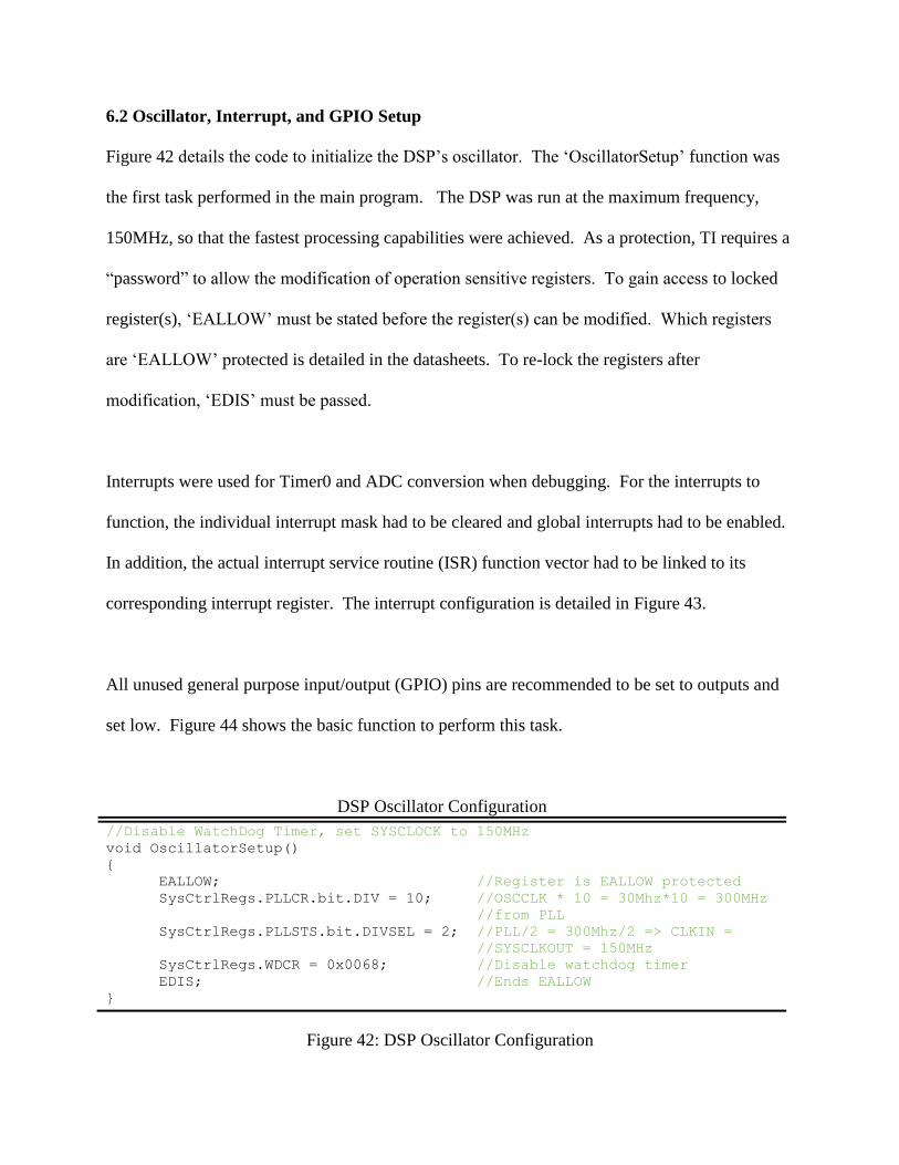
64
6.2 Oscillator, Interrupt, and GPIO Setup
Figure 42 details the code to initialize the DSP’s oscillator. The ‘OscillatorSetup’ function was
the first task performed in the main program. The DSP was run at the maximum frequency,
150MHz, so that the fastest processing capabilities were achieved. As a protection, TI requires a
“password” to allow the modification of operation sensitive registers. To gain access to locked
register(s), ‘EALLOW’ must be stated before the register(s) can be modified. Which registers
are ‘EALLOW’ protected is detailed in the datasheets. To re-lock the registers after
modification, ‘EDIS’ must be passed.
Interrupts were used for Timer0 and ADC conversion when debugging. For the interrupts to
function, the individual interrupt mask had to be cleared and global interrupts had to be enabled.
In addition, the actual interrupt service routine (ISR) function vector had to be linked to its
corresponding interrupt register. The interrupt configuration is detailed in Figure 43.
All unused general purpose input/output (GPIO) pins are recommended to be set to outputs and
set low. Figure 44 shows the basic function to perform this task.
DSP Oscillator Configuration
//Disable WatchDog Timer, set SYSCLOCK to 150MHz
void OscillatorSetup()
EALLOW; //Register is EALLOW protected
SysCtrlRegs.PLLCR.bit.DIV = 10; //OSCCLK * 10 = 30Mhz*10 = 300MHz
//from PLL
SysCtrlRegs.PLLSTS.bit.DIVSEL = 2; //PLL/2 = 300Mhz/2 => CLKIN =
//SYSCLKOUT = 150MHz
SysCtrlRegs.WDCR = 0x0068; //Disable watchdog timer
EDIS; //Ends EALLOW
Figure 42: DSP Oscillator Configuration

65
DSP Interrupt Configuration
void InterruptSetup()
DINT; //Disable global Interrupts
EALLOW; //Pie Vector Table is EALLOW protected
PieVectTable.TINT0 = &Timer0_ISR;//Link Timer0 to interrupt vector
PieVectTable.SEQ1INT = &Adc_ISR; //Link ADC to interrupt vector
EDIS; //End EALLOW;
PieCtrlRegs.PIECTRL.bit.ENPIE = 1; //Enable Pie vector fetching
PieCtrlRegs.PIEIER1.bit.INTx7 = 1; //Enable Timer0 Interrupt into
//PIE1 block
PieCtrlRegs.PIEACK.all = 0xFFFF; //Clear Acknowledgements
IER = 0x01; //Enable INT1 to CPU (timer0 in INT1)
EINT; //Enable Global Interrupts
Figure 43: DSP Interrupt Configuration
DSP GPIO Configuration
//Set all pins to low, outputs
void GpioSetup()
EALLOW; //Register is EALLOW protected
//Configure GPIO pins: outputs, lows, no pull-up resistor
GpioDataRegs.GPACLEAR.all = 0xFFFFFFFF; //Low output
GpioDataRegs.GPBCLEAR.all = 0xFFFFFFFF; //Low output
GpioDataRegs.GPCCLEAR.all = 0xFFFFFFFF; //Low output
GpioCtrlRegs.GPADIR.all = 0xFFFFFFFF; //Configure as outputs
GpioCtrlRegs.GPBDIR.all = 0xFFFFFFFF; //Configure as outputs
GpioCtrlRegs.GPCDIR.all = 0xFFFFFFFF; //Configure as outputs
EDIS; //Ends EALLOW protection
Figure 44: DSP GPIO Configuration
6.3 Timer0 Setup
Timer0 was used for two purposes: to provide a delay upon startup and to delay the acquisition
of data after a switching action. Upon DSP power up, a delay was implemented after the basic
configuration and ADC circuitry was powered on. This was intended to ensure everything was
stable before performing the control. When the gate signal changed, noise was generated on all

66
feedback signals. Therefore, to neglect the noise and prevent inaccurate readings, a time delay
was implemented after the gate signal changed, preventing the control calculations. A flag was
cleared and Timer0 activated when the switch changed states. Once Timer0 overflowed and
interrupted, the flag was set and the control code was allowed to continue to calculate until the
next switch transition. Figure 45 details the Timer0 configuration and interrupt service routine.
DSP Timer0 Configuration and Interrupt
//Enable Timer0 Interrupt, Set to period of 5ms
void Timer0Setup()
SysCtrlRegs.PCLKCR3.bit.CPUTIMER0ENCLK = 1; //Activate Peripheral
//CPU1 Timer Clock
CpuTimer0Regs.TCR.bit.TIE = 1; //Enable Timer0
//Interrupt at Peripheral Level
CpuTimer0Regs.PRD.all = 0x000C; //Main Counter
CpuTimer0Regs.TPR.bit.TDDR = 0xFF; //Prescale Value low
CpuTimer0Regs.TPRH.bit.TDDRH = 0xFF; //Prescale Value high
CpuTimer0Regs.TCR.bit.TRB = 1; //Reload the timer
CpuTimer0Regs.TCR.bit.TSS = 0; //Start the timer
//Reset Timer0, Turn off Timer0, disable timer0 interrupt, enable ADC
//interrupt, start ADC. If past startup, set new_data flag to allow control
interrupt void Timer0_ISR()
CpuTimer0Regs.TCR.bit.TIF = 1; //Writing 1 clears the flag
PieCtrlRegs.PIEACK.bit.ACK1 = 1; //Clears the acknowledgement for Int1
if(STABILIZE == 1)
STABILIZE = 0; //signify end of start up delay
CpuTimer0Regs.TCR.bit.TSS = 1; //Stop the timer
CpuTimer0Regs.PRD.all = 100; //Main Counter
CpuTimer0Regs.TPR.bit.TDDR = 0; //Prescale Value low
CpuTimer0Regs.TPRH.bit.TDDRH = 0; //Prescale Value high
CpuTimer0Regs.TCR.bit.TRB = 1; //Reload the timer
else if(STARTUP == 0) //used to prevent inaccurate data during noise
CpuTimer0Regs.TCR.bit.TSS = 1; //Stop the timer
CpuTimer0Regs.PRD.all = 700; //Main Counter
CpuTimer0Regs.TCR.bit.TRB = 1; //Reload the timer
NEW_DATA = 1; //set flag
Figure 45: DSP Timer0 Configuration and Interupt

67
6.4 ADC Configuration and Interrupt
The ADC was configured to perform eight conversions in a sequence: output current once,
secondary current once, primary current twice, and output voltage four times. The primary
current and output current were oversampled to perform averaging on a sample basis. These two
variables were selected to be averaged due to the sensitivity of the control to these variables
compared to the secondary and output current. The ADC was configured in continuous sample
mode meaning as soon as the 8 conversion sequence was completed, it restarted the sequence
without needing to be told to do so. The ADC clock was also configured to the highest setting of
25MHz. TI programs each DSP with a unique calibration sequence as it comes off the assembly
line when manufactured. This calibration is called by the ‘ADC_cal()’ function to ensure ADC
accuracy. Figure 46 details the ADC configuration function.
The ADC interrupt was not used during normal operation but occasionally used for debugging
purposes. Testing performed with the ADC interrupt included toggling a GPIO pin to see the
conversion sequence period. Figure 46 details the ADC interrupt.

68
DSP ADC Configuration and Interrupt
void AdcSetup()
//ADC Clock Setup
EALLOW; //Registers are EALLOW protected
SysCtrlRegs.HISPCP.bit.HSPCLK = 3; //High Speed Clock,
//HSPCLK, = SYSCLKOUT/6 = 150MHz/6 = 25MHz
AdcRegs.ADCTRL1.bit.CPS = 0; //ADC prescaler of 1
//–> ADC Clock = 25MHz
SysCtrlRegs.PCLKCR0.bit.ADCENCLK = 1; //Activate ADC Clock
EDIS;
//Calibration and General Startup
AdcRegs.ADCTRL3.bit.ADCBGRFDN = 3; //Power up ADC Bandgap reference
AdcRegs.ADCTRL3.bit.ADCPWDN = 1; //Power up ADC circuitry
ADC_cal(); //Calls factory calibration procedure
AdcRegs.ADCMAXCONV.bit.MAX_CONV1 = 7; //8 Conversions Take Place
AdcRegs.ADCTRL1.bit.ACQ_PS = 20; //S/H window 1 * 25Mhz period
//Choose which channels to convert in which order
AdcRegs.ADCCHSELSEQ1.bit.CONV00 = 4; //Vo
AdcRegs.ADCCHSELSEQ1.bit.CONV01 = 3; //Ip
AdcRegs.ADCCHSELSEQ1.bit.CONV02 = 4; //Vo
AdcRegs.ADCCHSELSEQ1.bit.CONV03 = 2; //Io
AdcRegs.ADCCHSELSEQ2.bit.CONV04 = 4; //Vo
AdcRegs.ADCCHSELSEQ2.bit.CONV05 = 5; //Is
AdcRegs.ADCCHSELSEQ2.bit.CONV06 = 4; //Vo
AdcRegs.ADCCHSELSEQ2.bit.CONV07 = 3; //Ip
//Adc Interrupt Setup
AdcRegs.ADCTRL2.bit.INT_MOD_SEQ1 = 0;//Seq1 Interrupt at every EOC
AdcRegs.ADCTRL2.bit.INT_ENA_SEQ1 = 1;//Seq1 Interrupts enabled
AdcRegs.ADCTRL1.bit.SUSMOD = 2; //ADC stops after current conversion
// when debugger hits breakpoint
AdcRegs.ADCTRL1.bit.CONT_RUN = 1; //allows continuous running
AdcRegs.ADCTRL2.bit.RST_SEQ1 = 1; //Reset Seq1
//used for sequence period measurement
interrupt void Adc_ISR()
AdcRegs.ADCST.bit.INT_SEQ1_CLR = 1; //Clear Interrupt Flag
PieCtrlRegs.PIEACK.bit.ACK1 = 1;//Clears the acknowledgement for Int
AdcRegs.ADCTRL2.bit.RST_SEQ1 = 1; //Reset Seq1
AdcRegs.ADCTRL2.bit.SOC_SEQ1 = 1; //Start Seq1 conversion
GpioDataRegs.GPATOGGLE.bit.GPIO20 = 1; //Set Pin if toggle desired
Figure 46: DSP ADC Configuration and Interrupt
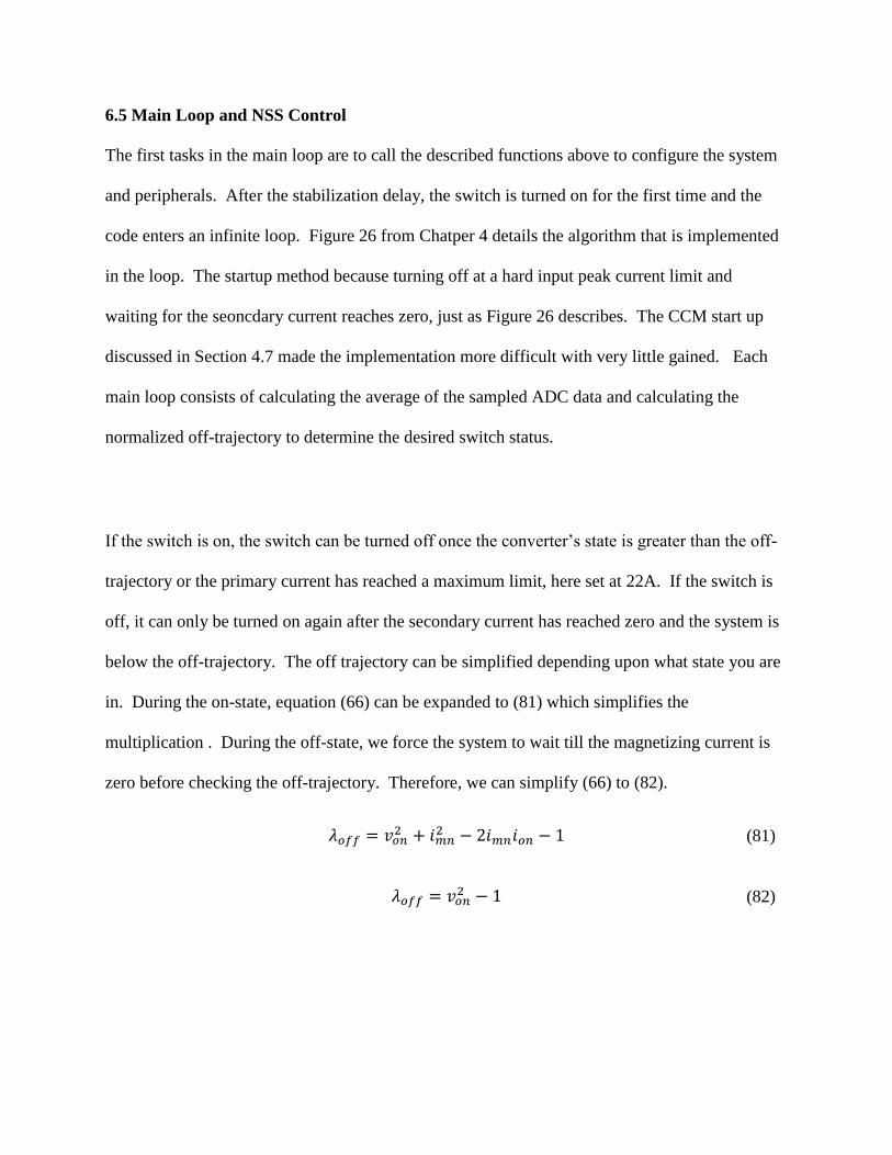
69
6.5 Main Loop and NSS Control
The first tasks in the main loop are to call the described functions above to configure the system
and peripherals. After the stabilization delay, the switch is turned on for the first time and the
code enters an infinite loop. Figure 26 from Chatper 4 details the algorithm that is implemented
in the loop. The startup method because turning off at a hard input peak current limit and
waiting for the seoncdary current reaches zero, just as Figure 26 describes. The CCM start up
discussed in Section 4.7 made the implementation more difficult with very little gained. Each
main loop consists of calculating the average of the sampled ADC data and calculating the
normalized off-trajectory to determine the desired switch status.
If the switch is on, the switch can be turned off once the converter’s state is greater than the off-
trajectory or the primary current has reached a maximum limit, here set at 22A. If the switch is
off, it can only be turned on again after the secondary current has reached zero and the system is
below the off-trajectory. The off trajectory can be simplified depending upon what state you are
in. During the on-state, equation (66) can be expanded to (81) which simplifies the
multiplication . During the off-state, we force the system to wait till the magnetizing current is
zero before checking the off-trajectory. Therefore, we can simplify (66) to (82).
𝜆𝑜𝑓𝑓 = 𝑣𝑜𝑛2 + 𝑖𝑚𝑛
2 − 2𝑖𝑚𝑛𝑖𝑜𝑛 − 1 (81)
𝜆𝑜𝑓𝑓 = 𝑣𝑜𝑛2 − 1 (82)

70
DSP Main Program Loop
int main()
OscillatorSetup(); //Clock Out is 150MHz, Watchdog Disabled
InterruptSetup(); //Enable Global Interrupts and Timer0
GpioSetup(); //Set all as low outputs
AdcSetup(); //Setup ADC
Timer0Setup(); //5ms Period, waiting for ADC to stabilize
long vo_array[4] = 0, 0, 0, 0; //vo average array
int i = 0; //vo array index
long long vo_total = 0; //running vo average array total
int vo_ave = 0; //vo average
long seq_ave = 0; //vo conversion sequence average
int ip_average = 0; //ip average
//dummy loop for stabilization from timer0
do
while(STABILIZE);
//switch on for first time
EALLOW; //allow registers to be modified continuously, no EDIS
GpioDataRegs.GPASET.bit.GPIO28 = 1; //Set Pin, gate signal
Q = 1; //Set flag
CpuTimer0Regs.TCR.bit.TSS = 0;//Start the timer to block calculations
AdcRegs.ADCTRL2.bit.SOC_SEQ1 = 1; //Start Seq1 conversion
//infinite main loop
while(1)
if(NEW_DATA == 1) //only calculates after switching noise gone
//average vo in this sequence
seq_ave = AdcMirror.ADCRESULT0;
seq_ave = seq_ave + AdcMirror.ADCRESULT2;
seq_ave = seq_ave + AdcMirror.ADCRESULT4;
seq_ave = seq_ave + AdcMirror.ADCRESULT6;
vo_ave = seq_ave >> 2; //store vo average
//calculate a running sequence average. Round robbin
vo_total = vo_total + vo_ave;//add to total
vo_array[y] = vo_ave; //add to array
y++; //index array
if(y > 3) //loop around if past size
y = 0;
vo_ave = vo_total >> 4; //calculate the average
vo_total = vo_total - vo_array[y]; //remove last value
//average primary current for this sequence
ip_average = AdcMirror.ADCRESULT1;
ip_average = ip_average + AdcMirror.ADCRESULT7;
ip_average = ip_average >> 1;

71
if(Q == 1 && NEW_DATA == 1) //Switch is on, calculate boundary
//and compare if above or below
//off state trajectory
if((vo_ave*0.000366211+0.08)*(vo_ave*0.000366211+0.08)+(ip_average*
0.0000140477+0.00000211395)*(ip_average*0.0000140477+0.00000211395)-
2*(ip_average*0.0000140477+0.00000211395)*(AdcMirror.ADCRESULT3*
0.00000810274-0.0162190)-1 > 0.0)
GpioDataRegs.GPACLEAR.bit.GPIO28 = 1; //turn off switch
Q = 0; //set switch off flag
NEW_DATA = 0; //prevent calculations
CpuTimer0Regs.TCR.bit.TSS = 0; //Start the timer
//turn off if past peak limit
else if((ip_average*0.0058895) > 22.854)
GpioDataRegs.GPACLEAR.bit.GPIO28 = 1; //turn off switch
Q = 0; //set switch off
NEW_DATA = 0; //prevent calculations
CpuTimer0Regs.TCR.bit.TSS = 0; //Start the timer
//else, Q stays on
else if (Q == 0 && NEW_DATA == 1) //switch is off
//check for zero secondary current
if(AdcMirror.ADCRESULT5*0.000914063 - 0.6735 < 0.15018 )
//calculate simplified off trajectory
if((vo_ave*0.000366211+0.08)*(vo_ave*0.000366211+0.08) < 1)
GpioDataRegs.GPASET.bit.GPIO28 = 1; //Turn on switch
Q = 1; //Set switch on
NEW_DATA = 0; //prevent calculation
CpuTimer0Regs.TCR.bit.TSS = 0; //Start the timer
//else, Q stays off
//else, Q stays off
return 0;
Figure 47: DSP Main Program Loop

72
VII. Experimental Results
7.1 Sensor Calibration
Immediately upon testing, it was evident that the transformer was not capable of transferring the
100W it was designed for. The transformer saturated, decreasing the magnetizing inductance,
and cause the input current to rise quickly. Therefore, the load on all testing was 500Ω, which is
equivalent to 90W during steady state.
Figure 48 shows the primary and secondary feedback current signals at the input of the ADC.
Each signal was simultaneously compared to its corresponding LEM sensor output to calculate
the gain equation for each channel. For the output voltage, a digital multi-meter was attached to
the output voltage while monitoring the output voltage feedback line. Data points were acquired
and a line of best fit was established. Since the load was known and purely resistive, the output
current was calibrated in the same way.
Figure 48: Primary and Secondary Feedback Signals using Function Generator
Blue-Secondary Current, Red-Primary Current

73
7.2 Main Loop Period
The main loop period was calculated by toggling a GPIO pin every cycle. Figure 49 shows this
toggle overlaid on the primary current feedback signal for reference. During the switching
transitions, the toggle frequency is greatly increased until Timer0 interrupts. This is due to the
NEW_DATA flag intentionally preventing the DSP from performing calculations during noisy
areas. It is also notable that the frequency of loops is faster during the off-state than the on-state.
This is due to the fact the off-trajectory calculation is greatly simplified in comparison to the on-
state. On average, the on-state period was approximately 1us and the off-state period was
approximately 600ns.
Figure 49: Main Loop Period Calculation
Red-GPIO Toggle, Blue-Primary Current

74
7.3 Steady State Primary and Secondary Feedback Signals
?? and ?? show two snap shots of what should be the steady state signals of the primary and
secondary currents. There is a slight oscillation of the current peak at times, instead of the
expected constant peak value. This could be coming from noise in the feedback lines or delays
in the program execution. Another possibility could be form the time delay introduced from
introducing a moving average on the output voltage. More research and debugging will need to
be performed to find the root of the issue.
Figure 50: Steady State Primary and Secondary Current with DSP Control
Blue-Primary Current, Red-Secondary Current

75
Figure 51: Steady State Currents Indicating Oscillation Error
Blue-Primary Current, Red-Secondary Current
7.4 Start Up Output Voltage
Figure 52 shows the output voltage during start up. To reach the steady state value of 200V it
takes approximately 35ms. This is extremely comparable to the simulated result with the same
startup method shown in Figure 24. Here, the simulated time to reach 200V was 34ms. The
experimental results show a slight overshoot of output voltage equivalent to less than 10V, but
no oscillation. During steady state, a digital multi metered connected to the output reads an AC
voltage ripple of only 200mV.

76
Figure 52: Start-up Output Voltage
7.5 Output Voltage Regulation to Input Voltage Drop
Figure 53 shows the stability of the NSS control. The input voltage was dropped 17V over
600ms. The output voltage is shifted 200V down the y-axis from the center grid so that the
signal could have a high enough gain for the output voltage change to be noticeable. Therefore,
the output voltage started at 200V before the input voltage change and ended at approximately
199V after the change. The NSS control successfully regulated the output voltage within an
acceptable tolerance to a wide input swing.
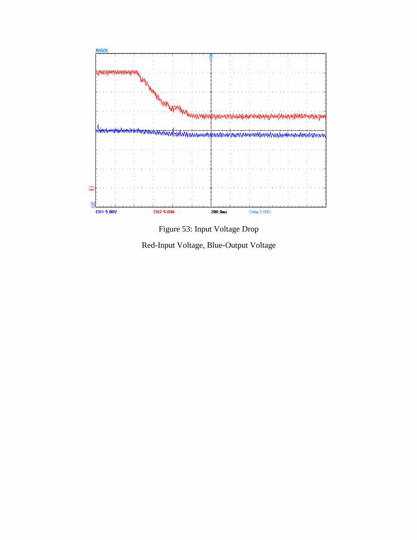
77
Figure 53: Input Voltage Drop
Red-Input Voltage, Blue-Output Voltage
78
Conclusion
This thesis covered from the derivation to the experimental testing of a flyback converter
implementing the Natural Switching Surface control method. The normalized NSS derivations
were detailed in Chapter 3 and the desired BCM control law was solved for in Chapter 4.
Following the derivations, the control law was simulated and validated in MATLAB/Simulink©
.
A 90W flyback converter prototype was designed and constructed, detailed in Chapter 5. The
NSS control law was developed in a DSP, explained in Chapter 6, and experimental results were
obtained and summarized in Chapter 7.
The NSS control adequately regulated the flyback converter. A steady state output voltage near
200V was reached and held. The flyback converter was able to recover from an input voltage
swing of 17V with only a 1V change on the output. The steady state primary and secondary
currents did have some errors. Where a constant peak current was expected on the currents
during steady state, an oscillatory nature was noticed. This could be induced by noise on the
feedback signals or delays in the DSP programming implementation. A downfall of this control
technique is that the converter is operating under variable frequency, making EMI considerations
more difficult.
Future research could include analyzing the effects of noise on the feedback signals and which
signals are more sensitive. Each variable in the off-trajectory is not weighted equal. Therefore,
a small change in a variable’s signal due to noise could introduce large output errors. Other
research could be an attempt to minimize needed sensors by using known state variables and
operation of the flyback converter and predicting the unknown variables.

79
References
[1] J. Picard, "Under the Hood of Flyback SMPS Designs," in Texas Instruments Power Supply
Design Seminar, 2010.
[2] M. Kazimierczuk and S. Nguyen, "Closed-loop voltage-mode-controlled PWM flyback dc-
dc converter for CCM with integral-lead controller," in Proceedings of the IEEE 1995
National Aerospace and Electronics Conference, 1995.
[3] S. L. Nalla, H. Hess, K. Buck and E. Mentze, "Flyback converter with voltage control mode
on chip for portable applications," in 2005 IEEE Workshop on Microelectronics and
Electron Devices, 2005.
[4] Linear Technology Corporation, "LTC3805 Adjustable Frequency Current Mode Flyback
DC/DC Controller," 2006.
[5] Semiconductor Components Industries, LLC, "NCP1234 Fixed Frequency Current Mode
Controller for Flyback Converters," 2011.
[6] M.-T. Lin, "A second order sliding mode controller for the Flyback converter," in 2014
IEEE International Conference on Systems, Man and Cybernetics, 2014.
[7] M. Salimi, J. Soltani, A. Zakipour and V. Hajbani, "Sliding mode control of the DC-DC
flyback converter with zero steady-state error," in Power Electronics, Drive Systems and
Technologies Conference, 2013.
[8] M. Ordonez, J. Quaicoe and M. Iqbal, "Advanced boundary control of inverters using the
natural switching surface: Normalized geometrical derivation," in IEEE Power Electronics
Specialists Conference, 2008.
[9] J. Galvez, M. Ordonez, T. Nguyen and F. Luchino, "Boundary control of buck-boost

80
converters: normalized trajectories and the Natural Switching Surface," in 2012 IEEE
Energy Conversion Congress and Exposition, 2012.
[10] L. A. Garcia Rodriguez and J. C. Balda, "A comparison of isolated DC-DC converters for
microinverter applications," in 2013 Twenty-Eighth Annual IEEE Applied Power
Electronics Conference and Exposition, 2013.
[11] S. J. Chapman, Electric Machinery Fundamentals, 5th ed., New York, New York: McGraw
Hill, 2012.
[12] S. Ang and A. Oliva, Power-Switching Converters, 3rd ed., Boca Raton, Florida: CRC
Press, 2011.
[13] M. V. Keni, "Development of an Isolated Flyback Converter Employing Boundary-Mode
Operation and Magnetic Flux Sensing Feedback," Massachusetts Institute of Technology,
2004.
[14] L. A. García Rodríguez, "Ph.D. Candidate," Fayetteville, 2014-2015.
[15] K. Berggren, LC Circuit, Natural Frequency, Characteristic Impedance, YouTube, 2013.
[16] M. Bourne, "Expressing a sin θ ± b cos θ in the form R sin(θ ± α)," Interactive Mathmatics,
10 1 2015. [Online]. Available: http://www.intmath.com/analytic-trigonometry/6-express-
sin-sum-angles.php.
[17] E. W. Weisstein, "Inverse Trigonometric Functions," MathWorld--A Wolfram Web
Resource, 2015. [Online]. Available:
http://mathworld.wolfram.com/InverseTrigonometricFunctions.html.
[18] Fairchild Semiconductor, "Application Note AN-4147: Design Guidelines for RCD Snubber
of Flyback Converters," 2006.

81
[19] Cree Inc., "C3D06060A Silicon Carbide Schottky Diode," 2013.
[20] N. Mohan and T. M. R. W. P. Underland, Power electronics : converters, applications, and
design, New York: Wiley, 1989.
[21] R. Patel and G. Fritz, "Switching Power Supply Review - 60 Watt Flyback Regulator,"
Texas Instruments, 2001.

82
Appendix A
Appendix A details the schematics used for the hardware implementation of the 90W flyback
converter prototype. The board design is also included in this appendix.

83
Figure 54: Main Hierarchical Schematic

84
Figure 55: Output Voltage Schematic

85
Figure 56: Input Voltage Schematic

86
Figure 57: MOSFET and Gate-Driver Schematic

87
Figure 58: Primary Current Schematic

88
Figure 59: Secondary and Output Current Schematic

89
Figure 60: Power Supply Schematic

90
Figure 61: Top of Allegro Board Layout

91
Figure 62: Bottom of Allegro Board Layout